US6725322B1 - Memory card, method for allotting logical address, and method for writing data - Google Patents
Memory card, method for allotting logical address, and method for writing dataDownload PDFInfo
- Publication number
- US6725322B1 US6725322B1US09/913,963US91396301AUS6725322B1US 6725322 B1US6725322 B1US 6725322B1US 91396301 AUS91396301 AUS 91396301AUS 6725322 B1US6725322 B1US 6725322B1
- Authority
- US
- United States
- Prior art keywords
- address
- starting
- data
- physical
- logical address
- Prior art date
- Legal status (The legal status is an assumption and is not a legal conclusion. Google has not performed a legal analysis and makes no representation as to the accuracy of the status listed.)
- Expired - Lifetime
Links
Images


Classifications
- G—PHYSICS
- G06—COMPUTING OR CALCULATING; COUNTING
- G06F—ELECTRIC DIGITAL DATA PROCESSING
- G06F12/00—Accessing, addressing or allocating within memory systems or architectures
- G06F12/02—Addressing or allocation; Relocation
- G—PHYSICS
- G06—COMPUTING OR CALCULATING; COUNTING
- G06F—ELECTRIC DIGITAL DATA PROCESSING
- G06F12/00—Accessing, addressing or allocating within memory systems or architectures
- G06F12/02—Addressing or allocation; Relocation
- G06F12/0223—User address space allocation, e.g. contiguous or non contiguous base addressing
- G06F12/023—Free address space management
- G06F12/0238—Memory management in non-volatile memory, e.g. resistive RAM or ferroelectric memory
- G06F12/0246—Memory management in non-volatile memory, e.g. resistive RAM or ferroelectric memory in block erasable memory, e.g. flash memory
- G—PHYSICS
- G06—COMPUTING OR CALCULATING; COUNTING
- G06F—ELECTRIC DIGITAL DATA PROCESSING
- G06F3/00—Input arrangements for transferring data to be processed into a form capable of being handled by the computer; Output arrangements for transferring data from processing unit to output unit, e.g. interface arrangements
- G06F3/06—Digital input from, or digital output to, record carriers, e.g. RAID, emulated record carriers or networked record carriers
- G06F3/0601—Interfaces specially adapted for storage systems
- G06F3/0602—Interfaces specially adapted for storage systems specifically adapted to achieve a particular effect
- G06F3/0614—Improving the reliability of storage systems
- G06F3/0616—Improving the reliability of storage systems in relation to life time, e.g. increasing Mean Time Between Failures [MTBF]
- G—PHYSICS
- G06—COMPUTING OR CALCULATING; COUNTING
- G06F—ELECTRIC DIGITAL DATA PROCESSING
- G06F3/00—Input arrangements for transferring data to be processed into a form capable of being handled by the computer; Output arrangements for transferring data from processing unit to output unit, e.g. interface arrangements
- G06F3/06—Digital input from, or digital output to, record carriers, e.g. RAID, emulated record carriers or networked record carriers
- G06F3/0601—Interfaces specially adapted for storage systems
- G06F3/0628—Interfaces specially adapted for storage systems making use of a particular technique
- G06F3/0638—Organizing or formatting or addressing of data
- G06F3/064—Management of blocks
- G—PHYSICS
- G06—COMPUTING OR CALCULATING; COUNTING
- G06F—ELECTRIC DIGITAL DATA PROCESSING
- G06F3/00—Input arrangements for transferring data to be processed into a form capable of being handled by the computer; Output arrangements for transferring data from processing unit to output unit, e.g. interface arrangements
- G06F3/06—Digital input from, or digital output to, record carriers, e.g. RAID, emulated record carriers or networked record carriers
- G06F3/0601—Interfaces specially adapted for storage systems
- G06F3/0668—Interfaces specially adapted for storage systems adopting a particular infrastructure
- G06F3/0671—In-line storage system
- G06F3/0673—Single storage device
- G06F3/0679—Non-volatile semiconductor memory device, e.g. flash memory, one time programmable memory [OTP]
- G—PHYSICS
- G11—INFORMATION STORAGE
- G11C—STATIC STORES
- G11C16/00—Erasable programmable read-only memories
- G11C16/02—Erasable programmable read-only memories electrically programmable
- G11C16/06—Auxiliary circuits, e.g. for writing into memory
- G11C16/10—Programming or data input circuits
- G11C16/14—Circuits for erasing electrically, e.g. erase voltage switching circuits
- G11C16/16—Circuits for erasing electrically, e.g. erase voltage switching circuits for erasing blocks, e.g. arrays, words, groups
Definitions
- the present inventionrelates to a technique of high-speed writing on a memory card, and particularly to a technique which is applied effectively to the allotment of logical address to a flash memory.
- memory cardsFor external memory devices of portable personal computers and multi-functional terminal units, memory cards have prevailed in a short time.
- the semiconductor memory included in a memory cardis, for example, a flash memory which is electrically erasable and rewritable and can hold a huge amount of data without the need of a battery.
- the flash memory used for the memory cardhas a data write operation in which before data is written to addresses, old data in the addresses is erased. This erasing operation takes place in a unit of sector (e.g., a sector has 512 bytes) or a unit of block (a block has 8 sectors, which have 4 k bytes).
- the memory cardtransacts data with a host unit in a unit of cluster (e.g., a cluster has 4 k bytes or 2 k bytes), and the flash memory reads or writes a cluster of data at a time.
- a host unite.g., a cluster has 4 k bytes or 2 k bytes
- the flash memoryreads or writes a cluster of data at a time.
- the memory cardis rendered the logical address allotment of the flash memory before it is shipped. Specifically, a data area for storing data to be transacted with the host unit is set next to an area for various control information including the master boot record, file allocation table and directories.
- the IC card of this kindis described in detail in, for example, publication “Electronic Materials”, pp. 22-26, edited by Masashi Ooshima, published by a company of Koogyo Choosa Kai on Dec. 1, 1990, and this publication describes the technical trend of various IC cards.
- logical addresses of clusters and those set to the flash memoryare out of accord with each other, which compels the abovementioned pre-writing data erasure to take place in a unit of sector or in units of sector and block in combination, resulting in an increased number of times of erasing operation and a longer data write time.
- the host unithas serial operations of data transfer, erasure and writing by expending time for each operation, which retards the speed-up of data writing to the flash memory.
- the present inventionis designed to use an offset storage section which stores an offset value and an offset calculation section which implements a computation for the offset value in the offset storing section and input logical addresses, and sets the logical addresses which are render the offset based on the calculation by the offset calculation section to physical addresses of the nonvolatile memory so that a unit of block and a unit of cluster match with each other.
- the present inventionis designed to have the abovementioned offset storage section included in an area of the nonvolatile memory.
- the present inventionis designed to store the offset value in the ID area of the nonvolatile memory.
- the present inventionis designed to form sector blocks each including physical addresses of a certain number of sectors of a nonvolatile memory, set the starting physical address of an arbitrary sector block among the sector blocks to the starting logical address of a data area, and set the data area of logical address down to the last sector of physical address.
- the present inventionis designed to form sector blocks each including physical addresses of a certain number of sectors of a nonvolatile memory, set the starting physical address of an arbitrary sector block among the sector blocks to the starting logical address of the data area, set the data area of logical address down to the last sector of physical address, and set the remaining data area to physical addresses by starting at the starting physical address.
- the present inventionis designed to form, for each of two nonvolatile memories, sector blocks each including physical addresses of a certain number of sectors, set the starting logical address of a data area to the starting physical address of an arbitrary sector block of one nonvolatile memory, set the remaining logical addresses to sector blocks of the two nonvolatile memories alternately on a block by block basis down to the last sectors of physical address of the two nonvolatile memories, and set the remaining data area to physical addresses of the one nonvolatile memory by starting at the starting physical address.
- the present inventionis designed to form, for each of nonvolatile memories of 2N in number, sector blocks each including physical addresses of a certain number of sectors, set the starting logical address of a data area to the starting physical address of an arbitrary sector block of one nonvolatile memory among the 2N nonvolatile memories, set the remaining logical addresses sequentially to sector blocks of the 2N nonvolatile memories on a block by block basis down to the last sectors of physical addresses of the 2N nonvolatile memories, and set the remaining data area to the one nonvolatile memory by starting at the starting physical address.
- the present inventionis designed to make the physical address of the sector block, to which the logical address is set, nearest to the starting address of the data area.
- the present inventionis designed to store data to be written, which is transferred from a host unit, on a memory card temporarily, read out control information from a block of a nonvolatile memory, erase the block, and store data to be written next, which is transferred from the host unit, on the memory card temporarily, while storing the data, which has been stored temporarily on the memory card, in the block-erased sectors of the nonvolatile memory.
- the present inventionis designed to include a first step of reading out control information from a sector block of a nonvolatile memory which firstly undergoes data writing and implementing the block erasure of the sector block, a second step of reading out control information from an arbitrary sector of the nonvolatile memory which secondly undergoes data writing, while storing data to be written, which has been stored temporarily on a memory card, into sectors of nonvolatile memory, and storing temporarily data to be written next on the memory card, and a third step, which takes place after control information is all read out of the sector block of the second-writing nonvolatile memory, of storing the data which has been stored temporarily on the memory card into sectors of the first-writing nonvolatile memory, while erasing the read-out sector block, and reading out control information from an arbitrary sector of the second-writing nonvolatile memory, with the second and third steps being repeated down to the nonvolatile memory of the 2N-th data writing.
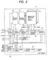
- FIG. 1is a block diagram of the memory card based on a first embodiment of this invention
- FIG. 2is a block diagram of the flash memory included in the memory card of the first embodiment of this invention
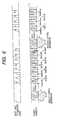
- FIG. 3is a diagram explaining the logical address of the memory card and the physical address which is fixed to the flash memory based on the first embodiment of this invention
- FIG. 4is a diagram explaining the flash memory address, with the logical address being set thereto, based on the first embodiment of this invention
- FIG. 5is a diagram explaining the flash memory address, with the logical address being set thereto, resulting from the study conducted by the inventors of the present invention
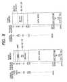
- FIG. 6is a timing chart of data writing on the memory card based on the first embodiment of this invention
- FIG. 1is a block diagram of the memory card based on a first embodiment of this invention
- FIG. 2is a block diagram of the flash memory included in the memory card of the first embodiment of this invention
- FIG. 3is a diagram explaining the logical address of the memory card and
- FIG. 7is a block diagram of the memory card based on a second embodiment of this invention
- FIG. 8is a diagram explaining the address of memory card, with the logical address being set thereto, based on the second embodiment of this invention
- FIG. 9is a diagram explaining the logical address which is set to the physical address based on the second embodiment of this invention
- FIG. 10is a timing chart of data writing on the memory card based on the second embodiment of this invention
- FIG. 11is a cross-sectional diagram of a memory cell transistor included in the memory card based on the first embodiment of this invention.
- the memory card 1is a flash memory card, which is used as external storage mediums of portable personal computers and multi-functional terminal units.
- the memory card 1is made up of an interface circuit 2 , microcomputer 3 and flash memory (nonvolatile memory) 4 , which are mounted on a printed circuit board.
- the interface circuit 2 and microcomputer 3constitute a controller.
- the memory card 1is put in and out of the PC card slot of a host unit such as a personal computer.
- the interface circuit 2includes a command register 5 , data register 6 , status register 7 , command decoder 8 , buffer memories 9 and 10 , and interface controller 11 .
- the microcomputer 3includes an interrupt control circuit 12 , microprocessor (including an offset calculator) 13 , ROM (Read Only Memory) 14 , RAM (Random Access Memory) 15 , timer 16 , and input/output port 17 .
- microprocessorincluding an offset calculator
- ROMRead Only Memory
- RAMRandom Access Memory
- the interface circuit 2is linked through the PC card slot to the host unit, which gives a file operation command to the command register 5 and it is decoded by the command decoder 8 .
- the command decoder 8releases interrupt signals IRQ 1 -IRQn depending on the decoding result.
- the interrupt control circuit 12gives the interrupt signals IRQ 1 -IRQn to the microprocessor 13 .
- the ROM 14stores an operation program of the microprocessor 13 , which runs the program by using the RAM 15 for the work area.
- the microprocessor 13controls the interface circuit 2 and flash memory 4 through the input/output port 17 in accordance with the operation program.
- the microcomputer 3releases the address signal ADRS, address strobe signal ASb, read signal RDb and write signal WRb to the interface controller 11 to transact data (DATA) with it.
- the microcomputer 3makes access to the data register 6 , status register 7 and buffer memories 9 and 10 through the interface controller 11 .
- the flash memory 4shares the control signal lines and data signal lines which are connected to the interface controller 11 .
- the microcomputer 3releases the chip enable signals CE of individual chips of flash memory 4 from the input/output port 17 .
- the microcomputer 3selects a chip of flash memory 4 , releases an address signal ADRS, address strobe signal ASb, read signal RDb and write signal WRb to the interface controller 11 , thereby making access to the selected chip of flash memory 4 by way of the interface controller 11 .
- the flash memory 4will be explained with reference to FIG. 2 .
- the flash memory 4includes a memory array 18 , x-address decoder 19 , x-address buffer 20 , multiplexer 21 , input buffer 22 , data control circuit 23 , y gate array 24 , y-address decoder 25 , output buffer 26 , y-address counter 27 , control signal buffer circuit 28 , mode control circuit 29 , and internal power circuit 30 .
- the memory array 18includes a memory mat and sense-latch circuit.
- the memory mathas numerous memory cells of transistors which are nonvolatile and electrically erasable and rewritable.
- each memory cell transistor Tr of the memory array 18has a source S and drain D which are formed in the semiconductor substrate or memory well SUB, a floating gate FG which is formed in the channel region by being interposed by a tunnel oxide film, and a control gate CG which is formed on the floating gate FG by being interposed by an inter-layer insulating film.
- the control gate CGis connected to a word line (shown in FIG. 2 ), and the drain D is connected to a bit line (shown in FIG. 2 ).
- Input/output terminals I/O 0 -I/O 7are used commonly for the address input terminals, data input terminals and command input terminals.
- the x-address signal received on the input/output terminals I/O 0 -I/O 7is put in the x-address buffer 20 via the multiplexer 21 .
- the x-address buffer 20releases internal complementary address signals, which are decoded by the x-address decoder to drive the word lines.
- the y-address decoder 25releases a select signal, based on which the y gate array 24 selects bit lines.
- the y-address signal received on the input/output terminals I/O 0 -I/O 7is preset to the y-address counter 27 , which increments the contents and puts the resulting y-address signal in the y-address decoder 25 .
- the bit lines selected by the y gate array 24are made conductive to the input section of the output buffer 26 during the data output operation, or made conductive to the output terminals of the input buffer 22 via the data control circuit 23 during the data input operation.
- the connection of the output buffer 26 and input buffer 22 with the input/output terminals I/O 0 -I/O 7is controlled by the multiplexer 21 .
- Command signals received on the input/output terminals I/O 0 -I/O 7are put in the mode control circuit 29 via the multiplexer 21 and input buffer 22 .
- the data control circuit 23provides the memory array 18 with data of logic values which are in accordance with the control of mode control circuit 29 , besides the data received on the input/output terminals I/O 0 -I/O 7 .
- the control signal buffer circuit 28receives external access control signals, which include a chip enable signal CEb, output enable signal OEb, write enable signal WEb, serial clock signal SC, reset signal RESb, and command enable signal CDEb.
- external access control signalsinclude a chip enable signal CEb, output enable signal OEb, write enable signal WEb, serial clock signal SC, reset signal RESb, and command enable signal CDEb.
- the mode control circuit 29controls the flash memory interface function in accordance with these control signals and also controls the internal operation of the flash memory 4 in accordance with the command.
- the internal power circuit 30produces various power voltages used for memory writing, erase-verification and reading, and supplies these power voltages to the x-address decoder 19 and memory cell arrays of the memory mats 18 .
- the logical addresses shown on the left side of FIG. 3have their leading section assigned to a system area for storing control data of the flash memory 4 .
- the system areacontains master boot record MBR, boot sector BS, file allocation tables FAT 1 and FAT 2 , and directories DR.
- the system areahas the allotment of logical addresses ranging 0h-4Ch (suffix “h” signifies hexadecimal).
- the system areais followed by a data area which ranges 4Dh-3D7Fh in terms of logical address for storing data transacted with the host unit.
- the data areais partitioned into sectors.
- the sectoris a unit area for data reading, writing and erasing.
- One sectorconsists of a user data area having a data length of 512 bytes and a control information area having a data length of 16 bytes.
- the allotment of logical address to the system area and data areais done at the time of formatting, which is based on MS-DOS (Microsoft Disk Operating System: registered trademark of Microsoft Corporation, USA) before the shipment of the memory card 1 .
- MS-DOSMicrosoft Disk Operating System: registered trademark of Microsoft Corporation, USA
- physical addresses 0h-3D7Fare used for the setting of logical addresses, and the remaining area starting at 3D80h is used for a defect table area for storing a defective sector table, a spare sector area for making access to a spare sector with reference to the defective sector table, an ID area for storing the memory card drive information ID (Identify Drive Information), and a CIS area for storing the memory card information CIS (Card Information Structure) including the name, type and function of memory card.
- the defective sector table area, ID area and CIS areacannot be accessed by the user.
- the physical addressesare partitioned from the starting address sequentially into blocks (a block has 8 sectors, which have 4 k bytes).
- the data areastarts at logical address 4Dh.
- This addresscorresponds most closely to the block starting address of physical address 50h, and clusters of data area are set to blocks by making the data area starting address 4Dh correspondent to the block starting address 50h.
- logical address 0his set by being offset to physical address 3h, and data in a unit of cluster (4 k bytes or 2 k bytes) sent from the host unit match with blocks.
- the offset valueis stored in advance in an area, e.g., ID area, of the flash memory 4 , and it is read out by the microprocessor 13 and loaded into the RAM 15 when power is turned on.
- the logical address value used by the host unitis converted into the physical address value based on the calculation by the microprocessor 13 by use of the offset value stored in the RAM 15 .
- FIG. 4shows the result of setting of the logical addresses, with the offset being put thereon, to the physical addresses of the flash memory 4 .
- the data area which starts at logical address 4Dhis set to the physical addresses by starting at address 50h which is the starting address of a block, with the last logical addresses 3D7Dh-Dh7Fh being brought back to the top of physical address and set to addresses 0h-2h.
- FIG. 5shows the logical address setting scheme examined by the inventors of the present invention, in which logical addresses are set directly to physical addresses.
- the data areastarts at logical address 4Dh, and it also starts at physical address 4Dh.
- the physical addressesare partitioned from the starting address 0h sequentially into blocks (a block has 8 sectors, which have 4 k bytes) as in the case of the first embodiment. In this case, however, the physical address 4Dh is an intermediate address of a block and therefore the cluster and block do not match in their starting addresses.
- block erasuretakes place only for the block of physical addresses 50h-57h, and the remaining block of 8 sectors needs to be erased by sector erasure.
- the resulting 9 erasing operationsincrease the data erase time significantly.
- the host unittransfers data T 1 of one sector to the buffer memory of the memory card 1 .
- the controller of the memory card 1reads out control information of the sectors S 1 -S 8 of the flash memory 4 to be written and, on detecting their normality, implements block erasure to erase all data of the sectors S 1 -S 8 at once.
- the transferred data T 1is loaded into the input buffer of the flash memory 4 , and data writing (writing 1 ) takes place. During the write operation, the host unit transfers data T 2 to be written next.
- the host unittransfers data T 3 to be written next.
- the logical addressis set to the physical address of the flash memory 4 by being offset so that the block areas and cluster areas match, allowing block erasure of data of the flash memory 4 , whereby the number of erasing operations at data writing can be reduced significantly.
- data writing to the flash memory 4 and data reception from the host unitare carried out concurrently, whereby the data write time can be reduced significantly.
- the memory card 1 ais made up of an interface circuit 2 , microcomputer 3 and flash memories 4 and 4 a .
- this memory card 1 ahas the additional provision of the flash memory 4 a , besides the interface circuit 2 , microcomputer 3 and flash memory 4 which are identical to those of the preceding first embodiment.
- the interface circuit 2includes a command register 5 , data register 6 , status register 7 , command decoder 8 , buffer memories 9 and 10 , and interface controller 11
- the microcomputer 3includes an interrupt control circuit 12 , microprocessor 13 , ROM 14 , RAM 15 , timer 16 , and input/output port 17 as in the case of the preceding first embodiment.
- the flash memories 4 and 4 a(nonvolatile memories) share the control signal lines and data signal lines which are connected to the interface controller 11 .
- the microcomputer 3releases the chip enable signals CE of the flash memories 4 and 4 a from the input/output port 17 .
- the microcomputer 3selects chips of flash memories 4 and 4 a , releases the address signal ADRS, address strobe signal ASb, read signal RDb and write signal WRb to the interface controller 11 , thereby making access to the selected chips of flash memories 4 and 4 a by way of the interface controller 11 .
- the flash memory 4 ais identical in arrangement to the flash memory 4 (shown in FIG. 2 ), and includes a memory array 18 , x-address decoder 19 , x-address buffer 20 , multiplexer 21 , input buffer 22 , data control circuit 23 , y gate array 24 , y-address decoder 25 , output buffer 26 , y-address counter 27 , control signal buffer circuit 28 , mode control circuit 29 , and internal power circuit 30 .
- FIG. 8shows on the left side the data structure of the flash memory 4 , with the logical address being set, and shows on the right side the data structure of the flash memory 4 a , with the logical address being set.
- the logical addresseshave their leading section assigned to a system area for storing control data of the flash memory 4 .
- the system areacontains master boot record MBR, boot sector BS, file allocation table FAT, and directories DR as in the case of the preceding first embodiment.
- the system areahas the setting of logical addresses ranging 0h-58h, and it is followed by a data area having the setting of logical addresses ranging 59h-7AFFh for storing data transacted with the host unit.
- the setting of logical address to the system area and data areais done at the time of MS-DOS formatting before the shipment of the memory card 1 as in the case of the preceding first embodiment.
- physical addresses 0h-3D7Fhare used for the setting of logical addresses, and the remaining area starting at 3D80h is used for a defect table area for storing a defective sector table, a spare sector area for making access to a spare sector with reference to the defective sector table, an ID area for storing the memory card drive information ID, and a CIS area for storing the memory card information CIS (Card Information Structure) including the name, type and function of memory card.
- CISCard Information Structure
- the physical addresses of the flash memories 4 and 4 aare partitioned from the starting address sequentially into blocks (a block has 8 sectors, which have 4 k bytes).
- the data area of the flash memory 4starts at logical address 59h as mentioned previously.
- This addresscorresponds most closely to the block starting address at physical address 30h, and the blocks starting at address 30h are assigned to the data area so that the data area starting address 59h corresponds to the block starting address 30h.
- the blocks of flash memory 4 starting at address 30hAfter the blocks of flash memory 4 starting at address 30h have been assigned to the data area, the blocks of flash memory 4 a starting at address 30h are assigned to the data area.
- the data areas of the flash memories 4 and 4 aare set alternately on a block by block basis. For example, as shown in FIG. 9, after logical addresses 59h-60h have been set to the flash memory 4 , the successive logical addresses 61h-68h are set to the flash memory 4 a.
- the logical addresses 7AF0h-7AFFhare set by being offset to the physical addresses 0h-6h for the flash memory 4 .
- the system areaalso has its logical addresses set in a unit of block of physical address.
- the block of addresses 0h-7his assigned to the data area of addresses 0h-6h, and a system area of one sector is set to this block.
- the master boot record MBRis set to physical address 7h of the flash memory 4 , and the successive boot sector BS, file allocation table FAT, and directories DR are set alternately on a block by block (8 sectors) basis to the flash memories 4 and 4 a.
- 16 sectors starting at logical address 59hi.e., a block of physical addresses 30h-37h of the flash memory 4 and another block of physical addresses 30h-37h of the flash memory 4 a , are erased by carrying out the erasing operation twice.
- the host unittransfers data T 1 of one sector to the buffer memory of the memory card 1 .
- the controller of the memory card 1reads out control information of the sectors S 1 -S 8 of the flash memory 4 a to be written and, on detecting their normality, implements block erasure to erase all data of the sectors S 1 -S 8 at once.
- the transferred data T 1is loaded into the input buffer of the flash memory 4 a , and data writing (writing 1 ) takes place.
- the host unittransfers data T 2 to be written next.
- the controller of the memory card 1reads control information out of the sector S 9 of the flash memory 4 .
- the next data T 2is loaded into the input buffer of the flash memory 4 , and data writing (writing 2 ) takes place.
- the host unittransfers data T 3 to be written next.
- the controller of the memory card 1reads control information out of the sector S 10 of the flash memory 4 .
- the transferred data T 6is loaded into the input buffer of the flash memory 4 , and data writing (writing 6 ) takes place.
- the controller of the memory card 1reads out control information of the sector S 15 and S 16 of the flash memory 4 . Control information of the sectors S 9 -S 16 for one block of the flash memory 4 is now read.
- the transferred data T 7is loaded into the input buffer of the flash memory 4 and written (writing 7 ), and during the transfer of data T 8 to be written next from the host unit, block erasure of data of the eight sectors of the flash memory 4 takes place.
- data writing and block erasure of the flash memories 4 and 4 a of the memory card 1can take place during the data transfer from the host unit, whereby the data write time can be reduced significantly.
- the second embodimentis the case of using two flash memories, it is also possible for other cases of flash memories of 2 n in number, which is more than four, to reduce the data write time significantly.
- the inventive memory card, method of logical address allotment and method of data writingare useful for the speed-up of data erasure and writing on the memory card.
Landscapes
- Engineering & Computer Science (AREA)
- Theoretical Computer Science (AREA)
- Physics & Mathematics (AREA)
- General Engineering & Computer Science (AREA)
- General Physics & Mathematics (AREA)
- Human Computer Interaction (AREA)
- Read Only Memory (AREA)
- Techniques For Improving Reliability Of Storages (AREA)
Abstract
Description
Claims (12)
Applications Claiming Priority (3)
| Application Number | Priority Date | Filing Date | Title |
|---|---|---|---|
| JP11-042518 | 1999-02-22 | ||
| JP4251899 | 1999-02-22 | ||
| PCT/JP2000/000827WO2000050997A1 (en) | 1999-02-22 | 2000-02-15 | Memory card, method for allotting logical address, and method for writing data |
Publications (1)
| Publication Number | Publication Date |
|---|---|
| US6725322B1true US6725322B1 (en) | 2004-04-20 |
Family
ID=12638311
Family Applications (1)
| Application Number | Title | Priority Date | Filing Date |
|---|---|---|---|
| US09/913,963Expired - LifetimeUS6725322B1 (en) | 1999-02-22 | 2000-02-15 | Memory card, method for allotting logical address, and method for writing data |
Country Status (6)
| Country | Link |
|---|---|
| US (1) | US6725322B1 (en) |
| EP (1) | EP1209568A1 (en) |
| JP (1) | JP4173642B2 (en) |
| KR (1) | KR100716576B1 (en) |
| TW (1) | TW502441B (en) |
| WO (1) | WO2000050997A1 (en) |
Cited By (29)
| Publication number | Priority date | Publication date | Assignee | Title |
|---|---|---|---|---|
| US20060020745A1 (en)* | 2004-07-21 | 2006-01-26 | Conley Kevin M | Fat analysis for optimized sequential cluster management |
| US20060039196A1 (en)* | 2003-10-03 | 2006-02-23 | Gorobets Sergey A | Corrected data storage and handling methods |
| US7023620B1 (en) | 2003-07-03 | 2006-04-04 | Research Electro-Optics, Inc. | Beam array pitch controller |
| US20060155922A1 (en)* | 2004-12-16 | 2006-07-13 | Gorobets Sergey A | Non-volatile memory and method with improved indexing for scratch pad and update blocks |
| US20060155921A1 (en)* | 2004-12-16 | 2006-07-13 | Gorobets Sergey A | Non-volatile memory and method with multi-stream update tracking |
| US20060155920A1 (en)* | 2004-12-16 | 2006-07-13 | Smith Peter J | Non-volatile memory and method with multi-stream updating |
| US20060161722A1 (en)* | 2004-12-16 | 2006-07-20 | Bennett Alan D | Scratch pad block |
| US20060221719A1 (en)* | 2003-09-18 | 2006-10-05 | Takuji Maeda | Semiconductor memory card, semiconductor memory control apparatus, and semiconductor memory control method |
| US20060253643A1 (en)* | 2005-05-04 | 2006-11-09 | Delkin Devices, Inc. | Memory with isolated master boot record |
| US20070033325A1 (en)* | 2005-08-03 | 2007-02-08 | Sinclair Alan W | Non-volatile memory with scheduled reclaim operations |
| US7395404B2 (en) | 2004-12-16 | 2008-07-01 | Sandisk Corporation | Cluster auto-alignment for storing addressable data packets in a non-volatile memory array |
| US20090055655A1 (en)* | 2002-11-27 | 2009-02-26 | Aran Ziv | Apparatus and Method For Securing Data on a Portable Storage Device |
| US20090254762A1 (en)* | 2008-04-04 | 2009-10-08 | Arik Priel | Access control for a memory device |
| US20090300271A1 (en)* | 2008-05-27 | 2009-12-03 | Phison Electronics Corp. | Storage system having multiple non-volatile memories, and controller and access method thereof |
| US7647470B2 (en)* | 2004-08-31 | 2010-01-12 | Sony Corporation | Memory device and controlling method for elongating the life of nonvolatile memory |
| US20100125698A1 (en)* | 2008-11-19 | 2010-05-20 | Akihisa Fujimoto | Recordable memory device |
| US20100191896A1 (en)* | 2009-01-23 | 2010-07-29 | Magic Technologies, Inc. | Solid state drive controller with fast NVRAM buffer and non-volatile tables |
| US20100226176A1 (en)* | 2005-04-01 | 2010-09-09 | Yan Li | Method for Non-Volatile Memory With Background Data Latch Caching During Read Operations |
| US8015347B2 (en) | 2007-12-28 | 2011-09-06 | Kabushiki Kaisha Toshiba | Memory system and control method thereof |
| US20120140561A1 (en)* | 2010-12-01 | 2012-06-07 | Kabushiki Kaisha Toshiba | Memory device capable of improving write processing speed and memory control method |
| US20140050005A1 (en)* | 2012-08-16 | 2014-02-20 | Samsung Electronics Co., Ltd. | Nonvolatile memory apparatus and method of operating the same |
| US8683173B2 (en) | 2009-01-21 | 2014-03-25 | Micron Technology, Inc. | Logical address offset in response to detecting a memory formatting operation |
| US20140122972A1 (en)* | 2012-10-29 | 2014-05-01 | Sony Corporation | Storage control apparatus, storage apparatus, information processing system, and storage control method |
| USRE45486E1 (en)* | 2003-02-07 | 2015-04-21 | Memory Technologies Llc | Method for addressing a memory card, a system using a memory card, and a memory card |
| US9183143B2 (en) | 2011-08-01 | 2015-11-10 | Kabushiki Kaisha Toshiba | Memory device that specifies a size of a segment of write data |
| US9626287B2 (en) | 2009-01-21 | 2017-04-18 | Micron Technology, Inc. | Solid state memory formatting |
| US10877900B1 (en) | 2019-06-26 | 2020-12-29 | Western Digital Technologies, Inc. | Enabling faster and regulated device initialization times |
| US11436083B2 (en) | 2020-09-04 | 2022-09-06 | Western Digital Technologies, Inc. | Data address management in non-volatile memory |
| US11527300B2 (en) | 2020-08-26 | 2022-12-13 | Western Digital Technologies, Inc. | Level dependent error correction code protection in multi-level non-volatile memory |
Families Citing this family (9)
| Publication number | Priority date | Publication date | Assignee | Title |
|---|---|---|---|---|
| JP4534336B2 (en)* | 2000-10-13 | 2010-09-01 | ソニー株式会社 | Data management method in memory device |
| JP2003296177A (en) | 2002-04-03 | 2003-10-17 | Sony Corp | Recording device and method, storage medium and program |
| US6898680B2 (en) | 2003-01-03 | 2005-05-24 | Micrel, Incorporated | Minimization of overhead of non-volatile memory operation |
| EP1653362B1 (en)* | 2003-08-06 | 2015-09-30 | Panasonic Corporation | Accessing device and method for a semiconductor memory card |
| US7158421B2 (en) | 2005-04-01 | 2007-01-02 | Sandisk Corporation | Use of data latches in multi-phase programming of non-volatile memories |
| WO2007130976A2 (en)* | 2006-05-05 | 2007-11-15 | Sandisk Corporation | Non-volatile memory with background data latch caching during program operations and methods therefor |
| TWI427637B (en)* | 2006-05-05 | 2014-02-21 | Sandisk Technologies Inc | Non-volatile memory with background data latch caching during program operations and methods therefor |
| WO2007131059A2 (en)* | 2006-05-05 | 2007-11-15 | Sandisk Corporation | Non-volatile memory with background data latch caching during erase operations and methods therefor |
| US11113188B2 (en) | 2019-08-21 | 2021-09-07 | Microsoft Technology Licensing, Llc | Data preservation using memory aperture flush order |
Citations (9)
| Publication number | Priority date | Publication date | Assignee | Title |
|---|---|---|---|---|
| JPH0527924A (en) | 1991-07-12 | 1993-02-05 | Internatl Business Mach Corp <Ibm> | External storage system using semiconductor memory and control method thereof |
| EP0557736A2 (en) | 1992-01-29 | 1993-09-01 | Microsoft Corporation | A method and system for file system management using a flash-erasable, programmable, read-only memory |
| JPH06124175A (en) | 1992-08-28 | 1994-05-06 | Sharp Corp | Semiconductor disk device |
| US5598370A (en)* | 1993-02-24 | 1997-01-28 | International Business Machines Corporation | Nonvolatile memory with cluster-erase flash capability and solid state file apparatus using the same |
| US5630093A (en)* | 1990-12-31 | 1997-05-13 | Intel Corporation | Disk emulation for a non-volatile semiconductor memory utilizing a mapping table |
| JPH1044527A (en) | 1996-08-01 | 1998-02-17 | Fuji Xerox Co Ltd | Method for storing print data and printer |
| US5799168A (en) | 1996-01-05 | 1998-08-25 | M-Systems Flash Disk Pioneers Ltd. | Standardized flash controller |
| JPH1153248A (en) | 1997-08-04 | 1999-02-26 | Tokyo Electron Ltd | Data processing system, block erasure type storage medium and program recording medium |
| US6459644B2 (en)* | 2000-06-06 | 2002-10-01 | Hitachi, Ltd. | Semiconductor memory device with block alignment function |
Family Cites Families (1)
| Publication number | Priority date | Publication date | Assignee | Title |
|---|---|---|---|---|
| US9908177B2 (en)* | 2014-05-20 | 2018-03-06 | Raytheon Company | Method of making an object with a metal-non-metal seal |
- 2000
- 2000-02-15JPJP2000601529Apatent/JP4173642B2/ennot_activeExpired - Fee Related
- 2000-02-15KRKR1020017010223Apatent/KR100716576B1/ennot_activeExpired - Fee Related
- 2000-02-15WOPCT/JP2000/000827patent/WO2000050997A1/enactiveIP Right Grant
- 2000-02-15USUS09/913,963patent/US6725322B1/ennot_activeExpired - Lifetime
- 2000-02-15EPEP00902975Apatent/EP1209568A1/ennot_activeWithdrawn
- 2000-02-17TWTW089102731Apatent/TW502441B/ennot_activeIP Right Cessation
Patent Citations (9)
| Publication number | Priority date | Publication date | Assignee | Title |
|---|---|---|---|---|
| US5630093A (en)* | 1990-12-31 | 1997-05-13 | Intel Corporation | Disk emulation for a non-volatile semiconductor memory utilizing a mapping table |
| JPH0527924A (en) | 1991-07-12 | 1993-02-05 | Internatl Business Mach Corp <Ibm> | External storage system using semiconductor memory and control method thereof |
| EP0557736A2 (en) | 1992-01-29 | 1993-09-01 | Microsoft Corporation | A method and system for file system management using a flash-erasable, programmable, read-only memory |
| JPH06124175A (en) | 1992-08-28 | 1994-05-06 | Sharp Corp | Semiconductor disk device |
| US5598370A (en)* | 1993-02-24 | 1997-01-28 | International Business Machines Corporation | Nonvolatile memory with cluster-erase flash capability and solid state file apparatus using the same |
| US5799168A (en) | 1996-01-05 | 1998-08-25 | M-Systems Flash Disk Pioneers Ltd. | Standardized flash controller |
| JPH1044527A (en) | 1996-08-01 | 1998-02-17 | Fuji Xerox Co Ltd | Method for storing print data and printer |
| JPH1153248A (en) | 1997-08-04 | 1999-02-26 | Tokyo Electron Ltd | Data processing system, block erasure type storage medium and program recording medium |
| US6459644B2 (en)* | 2000-06-06 | 2002-10-01 | Hitachi, Ltd. | Semiconductor memory device with block alignment function |
Non-Patent Citations (1)
| Title |
|---|
| "Electronic Materials", pp. 22-26 edited by Masashi Ooshima published by a company of Koogyo Chosa Kai on Dec. 1, 1990 (English Translation attached). |
Cited By (68)
| Publication number | Priority date | Publication date | Assignee | Title |
|---|---|---|---|---|
| US7900063B2 (en) | 2002-11-27 | 2011-03-01 | Sandisk Il Ltd. | Apparatus and method for securing data on a portable storage device |
| US8694800B2 (en) | 2002-11-27 | 2014-04-08 | Sandisk Il Ltd. | Apparatus and method for securing data on a portable storage device |
| US20090119517A1 (en)* | 2002-11-27 | 2009-05-07 | Aran Ziv | Apparatus and Method for Securing Data on a Portable Storage Device |
| US8234500B2 (en) | 2002-11-27 | 2012-07-31 | Sandisk Il Ltd. | Apparatus and method for securing data on a portable storage device |
| US20110167489A1 (en)* | 2002-11-27 | 2011-07-07 | Aran Ziv | Apparatus and Method for Securing Data on a Portable Storage Device |
| US7941674B2 (en)* | 2002-11-27 | 2011-05-10 | Sandisk Il Ltd. | Apparatus and method for securing data on a portable storage device |
| US8103882B2 (en) | 2002-11-27 | 2012-01-24 | Sandisk Il Ltd. | Apparatus and method for securing data on a portable storage device |
| US20110035603A1 (en)* | 2002-11-27 | 2011-02-10 | Aran Ziv | Apparatus and Method for Securing Data on a Portable Storage Device |
| US20090055655A1 (en)* | 2002-11-27 | 2009-02-26 | Aran Ziv | Apparatus and Method For Securing Data on a Portable Storage Device |
| US20090119502A1 (en)* | 2002-11-27 | 2009-05-07 | Aran Ziv | Apparatus and Method for Securing Data on a Portable Storage Device |
| US8893263B2 (en) | 2002-11-27 | 2014-11-18 | Sandisk Il Ltd. | Apparatus and method for securing data on a portable storage device |
| USRE45486E1 (en)* | 2003-02-07 | 2015-04-21 | Memory Technologies Llc | Method for addressing a memory card, a system using a memory card, and a memory card |
| US7023620B1 (en) | 2003-07-03 | 2006-04-04 | Research Electro-Optics, Inc. | Beam array pitch controller |
| US20060221719A1 (en)* | 2003-09-18 | 2006-10-05 | Takuji Maeda | Semiconductor memory card, semiconductor memory control apparatus, and semiconductor memory control method |
| US7654466B2 (en) | 2003-09-18 | 2010-02-02 | Panasonic Corporation | Semiconductor memory card, semiconductor memory control apparatus, and semiconductor memory control method |
| US7173852B2 (en) | 2003-10-03 | 2007-02-06 | Sandisk Corporation | Corrected data storage and handling methods |
| US20060039196A1 (en)* | 2003-10-03 | 2006-02-23 | Gorobets Sergey A | Corrected data storage and handling methods |
| US20060020745A1 (en)* | 2004-07-21 | 2006-01-26 | Conley Kevin M | Fat analysis for optimized sequential cluster management |
| US8607016B2 (en)* | 2004-07-21 | 2013-12-10 | Sandisk Technologies Inc. | FAT analysis for optimized sequential cluster management |
| US7647470B2 (en)* | 2004-08-31 | 2010-01-12 | Sony Corporation | Memory device and controlling method for elongating the life of nonvolatile memory |
| US7366826B2 (en) | 2004-12-16 | 2008-04-29 | Sandisk Corporation | Non-volatile memory and method with multi-stream update tracking |
| US20060155921A1 (en)* | 2004-12-16 | 2006-07-13 | Gorobets Sergey A | Non-volatile memory and method with multi-stream update tracking |
| US7315916B2 (en) | 2004-12-16 | 2008-01-01 | Sandisk Corporation | Scratch pad block |
| US7386655B2 (en) | 2004-12-16 | 2008-06-10 | Sandisk Corporation | Non-volatile memory and method with improved indexing for scratch pad and update blocks |
| US8151035B2 (en) | 2004-12-16 | 2012-04-03 | Sandisk Technologies Inc. | Non-volatile memory and method with multi-stream updating |
| US7395404B2 (en) | 2004-12-16 | 2008-07-01 | Sandisk Corporation | Cluster auto-alignment for storing addressable data packets in a non-volatile memory array |
| TWI386801B (en)* | 2004-12-16 | 2013-02-21 | Sandisk Technologies Inc | Cluster auto-alignment |
| US20060155922A1 (en)* | 2004-12-16 | 2006-07-13 | Gorobets Sergey A | Non-volatile memory and method with improved indexing for scratch pad and update blocks |
| US20080301359A1 (en)* | 2004-12-16 | 2008-12-04 | Peter John Smith | Non-Volatile Memory and Method With Multi-Stream Updating |
| US20060161722A1 (en)* | 2004-12-16 | 2006-07-20 | Bennett Alan D | Scratch pad block |
| US20060155920A1 (en)* | 2004-12-16 | 2006-07-13 | Smith Peter J | Non-volatile memory and method with multi-stream updating |
| US7412560B2 (en) | 2004-12-16 | 2008-08-12 | Sandisk Corporation | Non-volatile memory and method with multi-stream updating |
| US8351269B2 (en) | 2005-04-01 | 2013-01-08 | SanDisk Technologies, Inc. | Method for non-volatile memory with background data latch caching during read operations |
| US20100226176A1 (en)* | 2005-04-01 | 2010-09-09 | Yan Li | Method for Non-Volatile Memory With Background Data Latch Caching During Read Operations |
| US8036041B2 (en) | 2005-04-01 | 2011-10-11 | Sandisk Technologies Inc. | Method for non-volatile memory with background data latch caching during read operations |
| US20060253643A1 (en)* | 2005-05-04 | 2006-11-09 | Delkin Devices, Inc. | Memory with isolated master boot record |
| WO2006119282A3 (en)* | 2005-05-04 | 2008-01-31 | Delkin Devices Inc | Memory with isolated master boot record |
| US7984084B2 (en)* | 2005-08-03 | 2011-07-19 | SanDisk Technologies, Inc. | Non-volatile memory with scheduled reclaim operations |
| US20070033325A1 (en)* | 2005-08-03 | 2007-02-08 | Sinclair Alan W | Non-volatile memory with scheduled reclaim operations |
| US9933941B2 (en) | 2007-12-28 | 2018-04-03 | Toshiba Memory Corporation | Memory system and control method thereof |
| US8015347B2 (en) | 2007-12-28 | 2011-09-06 | Kabushiki Kaisha Toshiba | Memory system and control method thereof |
| US9026724B2 (en) | 2007-12-28 | 2015-05-05 | Kabushiki Kaisha Toshiba | Memory system and control method thereof |
| US12229404B2 (en) | 2007-12-28 | 2025-02-18 | Kioxia Corporation | Memory system and control method thereof |
| US9483192B2 (en) | 2007-12-28 | 2016-11-01 | Kabushiki Kaisha Toshiba | Memory system and control method thereof |
| US11893237B2 (en) | 2007-12-28 | 2024-02-06 | Kioxia Corporation | Memory system and control method thereof |
| US11287975B2 (en) | 2007-12-28 | 2022-03-29 | Kioxia Corporation | Memory system and control method thereof |
| US9280292B2 (en) | 2007-12-28 | 2016-03-08 | Kabushiki Kaisha Toshiba | Memory system and control method thereof |
| US8886868B2 (en) | 2007-12-28 | 2014-11-11 | Kabushiki Kaisha Toshiba | Memory system and control method thereof |
| US10558360B2 (en) | 2007-12-28 | 2020-02-11 | Toshiba Memory Corporation | Memory system and control method thereof |
| US8695087B2 (en) | 2008-04-04 | 2014-04-08 | Sandisk Il Ltd. | Access control for a memory device |
| US20090254762A1 (en)* | 2008-04-04 | 2009-10-08 | Arik Priel | Access control for a memory device |
| US20090300271A1 (en)* | 2008-05-27 | 2009-12-03 | Phison Electronics Corp. | Storage system having multiple non-volatile memories, and controller and access method thereof |
| US7975096B2 (en)* | 2008-05-27 | 2011-07-05 | Phison Electronics Corp. | Storage system having multiple non-volatile memories, and controller and access method thereof |
| US20100125698A1 (en)* | 2008-11-19 | 2010-05-20 | Akihisa Fujimoto | Recordable memory device |
| US8489802B2 (en)* | 2008-11-19 | 2013-07-16 | Kabushiki Kaisha Toshiba | Recordable memory device which writes data to reformatted user area of nonvolatile semiconductor memory |
| US8930671B2 (en) | 2009-01-21 | 2015-01-06 | Micron Technology, Inc. | Logical address offset in response to detecting a memory formatting operation |
| US9626287B2 (en) | 2009-01-21 | 2017-04-18 | Micron Technology, Inc. | Solid state memory formatting |
| US8683173B2 (en) | 2009-01-21 | 2014-03-25 | Micron Technology, Inc. | Logical address offset in response to detecting a memory formatting operation |
| US20100191896A1 (en)* | 2009-01-23 | 2010-07-29 | Magic Technologies, Inc. | Solid state drive controller with fast NVRAM buffer and non-volatile tables |
| US20120140561A1 (en)* | 2010-12-01 | 2012-06-07 | Kabushiki Kaisha Toshiba | Memory device capable of improving write processing speed and memory control method |
| US8856468B2 (en)* | 2010-12-01 | 2014-10-07 | Kabushiki Kaisha Toshiba | Memory device capable of improving write processing speed and memory control method |
| US9183143B2 (en) | 2011-08-01 | 2015-11-10 | Kabushiki Kaisha Toshiba | Memory device that specifies a size of a segment of write data |
| US20140050005A1 (en)* | 2012-08-16 | 2014-02-20 | Samsung Electronics Co., Ltd. | Nonvolatile memory apparatus and method of operating the same |
| US9176811B2 (en)* | 2012-10-29 | 2015-11-03 | Sony Corporation | Storage control apparatus, storage apparatus, information processing system, and storage control method |
| US20140122972A1 (en)* | 2012-10-29 | 2014-05-01 | Sony Corporation | Storage control apparatus, storage apparatus, information processing system, and storage control method |
| US10877900B1 (en) | 2019-06-26 | 2020-12-29 | Western Digital Technologies, Inc. | Enabling faster and regulated device initialization times |
| US11527300B2 (en) | 2020-08-26 | 2022-12-13 | Western Digital Technologies, Inc. | Level dependent error correction code protection in multi-level non-volatile memory |
| US11436083B2 (en) | 2020-09-04 | 2022-09-06 | Western Digital Technologies, Inc. | Data address management in non-volatile memory |
Also Published As
| Publication number | Publication date |
|---|---|
| EP1209568A1 (en) | 2002-05-29 |
| KR20010108209A (en) | 2001-12-07 |
| JP4173642B2 (en) | 2008-10-29 |
| TW502441B (en) | 2002-09-11 |
| KR100716576B1 (en) | 2007-05-11 |
| WO2000050997A1 (en) | 2000-08-31 |
Similar Documents
| Publication | Publication Date | Title |
|---|---|---|
| US6725322B1 (en) | Memory card, method for allotting logical address, and method for writing data | |
| EP1242868B1 (en) | Organization of blocks within a nonvolatile memory unit to effectively decrease sector write operation time | |
| US8320200B2 (en) | Semiconductor storage device and method of reading data therefrom | |
| US7290198B2 (en) | Memory card and memory controller | |
| US8429313B2 (en) | Configurable ready/busy control | |
| EP2345037B1 (en) | Translation layer in a solid state storage device | |
| US8681552B2 (en) | System and method for accessing and storing interleaved data | |
| US7937523B2 (en) | Memory system with nonvolatile semiconductor memory | |
| US7392343B2 (en) | Memory card having a storage cell and method of controlling the same | |
| US5379401A (en) | Flash memory card including circuitry for selectively providing masked and unmasked ready/busy output signals | |
| US9418017B2 (en) | Hot memory block table in a solid state storage device | |
| US5422855A (en) | Flash memory card with all zones chip enable circuitry | |
| US20020194451A1 (en) | Memory controller, flash memory system employing memory controller and method for controlling flash memory device | |
| US20060256610A1 (en) | Nonvolatile memory system using magneto-resistive random access memory (MRAM) | |
| JP2006040497A (en) | Semiconductor memory device, nonvolatile semiconductor memory device | |
| CN1198287C (en) | Low-voltage read cascode for 2V/3V and different bank combinations without metal options for simultaneous operation flash memory device | |
| US20060253643A1 (en) | Memory with isolated master boot record | |
| KR0180117B1 (en) | Non-volatile semiconductor memory | |
| JP2001176299A (en) | Nonvolatile semiconductor memory device |
Legal Events
| Date | Code | Title | Description |
|---|---|---|---|
| AS | Assignment | Owner name:HITACHI, LTD., JAPAN Free format text:ASSIGNMENT OF ASSIGNORS INTEREST;ASSIGNORS:SHIRAISHI, ATSUSHI;INOUE, MANABU;SHIOTA, SHIGEMASA;AND OTHERS;REEL/FRAME:012239/0888;SIGNING DATES FROM 20010612 TO 20010625 Owner name:HITACHI ULSI SYSTEMS CO.,LTD., JAPAN Free format text:ASSIGNMENT OF ASSIGNORS INTEREST;ASSIGNORS:SHIRAISHI, ATSUSHI;INOUE, MANABU;SHIOTA, SHIGEMASA;AND OTHERS;REEL/FRAME:012239/0888;SIGNING DATES FROM 20010612 TO 20010625 | |
| AS | Assignment | Owner name:RENESAS TECHNOLOGY CORPORATION, JAPAN Free format text:ASSIGNMENT OF ASSIGNORS INTEREST;ASSIGNOR:HITACHI, LTD.;REEL/FRAME:014190/0088 Effective date:20030912 | |
| STCF | Information on status: patent grant | Free format text:PATENTED CASE | |
| FEPP | Fee payment procedure | Free format text:PAYOR NUMBER ASSIGNED (ORIGINAL EVENT CODE: ASPN); ENTITY STATUS OF PATENT OWNER: LARGE ENTITY Free format text:PAYER NUMBER DE-ASSIGNED (ORIGINAL EVENT CODE: RMPN); ENTITY STATUS OF PATENT OWNER: LARGE ENTITY | |
| FPAY | Fee payment | Year of fee payment:4 | |
| AS | Assignment | Owner name:NEC ELECTRONICS CORPORATION, JAPAN Free format text:MERGER;ASSIGNOR:RENESAS TECHNOLOGY CORP.;REEL/FRAME:024879/0190 Effective date:20100401 Owner name:RENESAS ELECTRONICS CORPORATION, JAPAN Free format text:CHANGE OF NAME;ASSIGNOR:NEC ELECTRONICS CORPORATION;REEL/FRAME:024864/0635 Effective date:20100401 | |
| FPAY | Fee payment | Year of fee payment:8 | |
| AS | Assignment | Owner name:RENESAS ELECTRONICS CORPORATION, JAPAN Free format text:ASSIGNMENT OF ASSIGNORS INTEREST;ASSIGNOR:HITACHI ULSI SYSTEMS CO., LTD.;REEL/FRAME:032859/0252 Effective date:20140326 | |
| FPAY | Fee payment | Year of fee payment:12 | |
| AS | Assignment | Owner name:RENESAS ELECTRONICS CORPORATION, JAPAN Free format text:CHANGE OF ADDRESS;ASSIGNOR:RENESAS ELECTRONICS CORPORATION;REEL/FRAME:044928/0001 Effective date:20150806 |