US6724684B2 - Apparatus for pipe latch control circuit in synchronous memory device - Google Patents
Apparatus for pipe latch control circuit in synchronous memory deviceDownload PDFInfo
- Publication number
- US6724684B2 US6724684B2US10/261,042US26104202AUS6724684B2US 6724684 B2US6724684 B2US 6724684B2US 26104202 AUS26104202 AUS 26104202AUS 6724684 B2US6724684 B2US 6724684B2
- Authority
- US
- United States
- Prior art keywords
- counting
- signal
- data output
- output buffer
- pipe
- Prior art date
- Legal status (The legal status is an assumption and is not a legal conclusion. Google has not performed a legal analysis and makes no representation as to the accuracy of the status listed.)
- Expired - Fee Related
Links
Images


Classifications
- G—PHYSICS
- G11—INFORMATION STORAGE
- G11C—STATIC STORES
- G11C7/00—Arrangements for writing information into, or reading information out from, a digital store
- G—PHYSICS
- G11—INFORMATION STORAGE
- G11C—STATIC STORES
- G11C7/00—Arrangements for writing information into, or reading information out from, a digital store
- G11C7/10—Input/output [I/O] data interface arrangements, e.g. I/O data control circuits, I/O data buffers
- G11C7/1078—Data input circuits, e.g. write amplifiers, data input buffers, data input registers, data input level conversion circuits
- G11C7/109—Control signal input circuits
- G—PHYSICS
- G11—INFORMATION STORAGE
- G11C—STATIC STORES
- G11C11/00—Digital stores characterised by the use of particular electric or magnetic storage elements; Storage elements therefor
- G11C11/21—Digital stores characterised by the use of particular electric or magnetic storage elements; Storage elements therefor using electric elements
- G11C11/34—Digital stores characterised by the use of particular electric or magnetic storage elements; Storage elements therefor using electric elements using semiconductor devices
- G11C11/40—Digital stores characterised by the use of particular electric or magnetic storage elements; Storage elements therefor using electric elements using semiconductor devices using transistors
- G11C11/401—Digital stores characterised by the use of particular electric or magnetic storage elements; Storage elements therefor using electric elements using semiconductor devices using transistors forming cells needing refreshing or charge regeneration, i.e. dynamic cells
- G11C11/4063—Auxiliary circuits, e.g. for addressing, decoding, driving, writing, sensing or timing
- G11C11/407—Auxiliary circuits, e.g. for addressing, decoding, driving, writing, sensing or timing for memory cells of the field-effect type
- G11C11/409—Read-write [R-W] circuits
- G11C11/4093—Input/output [I/O] data interface arrangements, e.g. data buffers
- G—PHYSICS
- G11—INFORMATION STORAGE
- G11C—STATIC STORES
- G11C7/00—Arrangements for writing information into, or reading information out from, a digital store
- G11C7/10—Input/output [I/O] data interface arrangements, e.g. I/O data control circuits, I/O data buffers
- G11C7/1015—Read-write modes for single port memories, i.e. having either a random port or a serial port
- G11C7/1039—Read-write modes for single port memories, i.e. having either a random port or a serial port using pipelining techniques, i.e. using latches between functional memory parts, e.g. row/column decoders, I/O buffers, sense amplifiers
- G—PHYSICS
- G11—INFORMATION STORAGE
- G11C—STATIC STORES
- G11C7/00—Arrangements for writing information into, or reading information out from, a digital store
- G11C7/10—Input/output [I/O] data interface arrangements, e.g. I/O data control circuits, I/O data buffers
- G11C7/1051—Data output circuits, e.g. read-out amplifiers, data output buffers, data output registers, data output level conversion circuits
- G11C7/1057—Data output buffers, e.g. comprising level conversion circuits, circuits for adapting load
- G—PHYSICS
- G11—INFORMATION STORAGE
- G11C—STATIC STORES
- G11C7/00—Arrangements for writing information into, or reading information out from, a digital store
- G11C7/10—Input/output [I/O] data interface arrangements, e.g. I/O data control circuits, I/O data buffers
- G11C7/1051—Data output circuits, e.g. read-out amplifiers, data output buffers, data output registers, data output level conversion circuits
- G11C7/1066—Output synchronization
- G—PHYSICS
- G11—INFORMATION STORAGE
- G11C—STATIC STORES
- G11C7/00—Arrangements for writing information into, or reading information out from, a digital store
- G11C7/10—Input/output [I/O] data interface arrangements, e.g. I/O data control circuits, I/O data buffers
- G11C7/1072—Input/output [I/O] data interface arrangements, e.g. I/O data control circuits, I/O data buffers for memories with random access ports synchronised on clock signal pulse trains, e.g. synchronous memories, self timed memories
- G—PHYSICS
- G11—INFORMATION STORAGE
- G11C—STATIC STORES
- G11C7/00—Arrangements for writing information into, or reading information out from, a digital store
- G11C7/10—Input/output [I/O] data interface arrangements, e.g. I/O data control circuits, I/O data buffers
- G11C7/1078—Data input circuits, e.g. write amplifiers, data input buffers, data input registers, data input level conversion circuits
Definitions
- the present inventionrelates to an apparatus for pipe latch control circuit in a synchronous memory device.
- Synchronous memoryis advantageous in that the operation is fast compared to general memory devices.
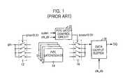
- FIG. 1is a block diagram of a synchronous memory data path utilizing an ordinary pipeline method in accordance with the prior art.
- the synchronous memory data pathincludes: four pipe latches 14 A through 14 D, a first switch 12 for selectively passing output data, which is applied from a global data bus gio to one of the pipe latches by pipe input control signals pinz ⁇ 0:3>, a data output buffer 18 for outputting the data to a data output terminal DQ using a data output buffer drive signal clk_do and a second switch 16 for selectively passing each output of the pipe latches 14 A through 14 D to the data output buffer 18 by pipe output control signals poutz ⁇ 0:3>.
- the pipe output control signals poutz ⁇ 0:3>are provided for controlling the output of the pipe latches 14 A through 14 D and they come from a pipe latch control circuit 10 , which inputs an output enable signal outen and a DLL clock signal clk_dll.
- the pipe latch 14 Ais divided into an even path and an odd path in the DDR SDRAM, because the global data bus gio is divided into an even data bus and an odd data bus. Furthermore, the pipe latch control circuit 10 is classified into even and odd parts.
- FIG. 2is a circuit diagram of the pipe latch control circuit in accordance with the prior art.
- the pipe latch control circuitis reset by a reset signal rstdoutz and starts counting when an increment signal outeninc is received.
- the pipe latch control circuitincludes an initial counting controller 20 for generating an initial counting signal.
- the rest of the unitsform four stage counters.
- Each counting stageincludes a transfer gate controlled by the increment signal, an inverter latch and an ordinary counter.
- FIG. 3is a timing chart of the pipe latch control circuit shown in FIG. 2 in accordance with the prior art.
- the burst length BLbe 4 when using the SDRAM and the burst length BL be 8 when using the DDR SDRAM.
- the increment signal outenincis generated by performing a NAND operation on the output enable signal outen and the DLL clock signal clk_dll. That is, the increment signal outeninc is generated by receiving the DLL clock signal clk_dll during the active cycle of the output enable signal outen.
- the output enable signal outenforms a window as much as the burst length for the data outputting the data.
- the increment signal outeninccontrols the transfer gate in order to output count signals k ⁇ 0:3> through the latch.
- the count signals k ⁇ 0:3>pass through three inverters to generate the pipe output control signals poutz ⁇ 0:3>. That is, the pipe output control signals poutz ⁇ 0:3> are enabled by synchronizing with a falling edge of the increment signal outeninc.
- the DLL clock signal clk_dllpasses through eight gates before the pipe control signals poutz ⁇ 0:3> appear as in FIG. 2 .
- the data output buffer drive signal clk_do for controlling the data output from a DQ pinis a delayed signal compared with the DLL clock signal clk_dll. Therefore, the data output buffer drive signal clk_do is enabled so that the data is outputted from the data output buffer within the enabling period of the pipe output control signals poutz ⁇ 0:3> under normal conditions.
- the data output buffer drive signal clk_doreceives the DLL clock signal clk_dll during the activation of the output enable signal outen.
- the operation timing of all semiconductor circuitsis greatly changed according to whether an operation condition is the best condition or the worst condition.
- the DLL clock signal clk_dllis disabled, since the pipe output output control signal poutz ⁇ 0:3> is generated by passing through 8 gates, a long delay time is caused. Specifically, a considerable difference of the delay time between the best condition and the worst condition can occur. Accordingly, in case of the worst condition, the corresponding data from the data output buffer may not be outputted completely within the enabling period of the pipe output control signals poutz ⁇ 0:3>. Therefore, the memory access time TAA should be limited for the complete data output. As an operation frequency increase, a loss of the memory access time TAA can be a serious problem.
- an apparatus for a pipe latch control circuit controlled by a pipe output control signal in a synchronous memory devicecomprising: a plurality of counting stages for counting in sequence in response to a data output buffer drive signal; and a counting signal drive means for generating the pipe output control signal by driving each counting signal, which is outputted from the plurality of counting stages and controlled by the data output buffer drive signal.
- FIG. 1is a block diagram of a synchronous memory data path utilizing an ordinary pipeline method in accordance with the prior art
- FIG. 2is a circuit diagram of a pipe latch control circuit shown in FIG. 1 in accordance with the prior art
- FIG. 3is a timing chart of the pipe latch control circuit shown in FIG. 2 in accordance with the prior art
- FIG. 4is a pipe latch control circuit diagram of a synchronous memory device in accordance with the present invention.
- FIG. 5is a timing chart of the pipe latch control circuit shown in FIG. 4 .
- FIG. 4is a pipe latch control circuit diagram of the synchronous memory device in accordance with the present invention.
- the pipe latch control circuitincludes an initial counting signal generator 40 for generating an initial counting signal and a NAND latch unit 44 having a plurality of counting stages for generating pipe control signals poutz ⁇ 0:3> by driving counting signals k ⁇ 0:3>.
- the initial counting signal generator 40is controlled by a reset signal rstdoutz and it is configured identically to the initial counting controller 20 of the pipe latch control circuit shown in FIG. 2 .
- Each counting stageincludes a transfer gate controlled by an increment signal outeninc_new, an inverter latch and an ordinary counter.
- the increment signal outeninc_newwhich controls the transfer gate of each counting stage, uses an inverting signal of a drive signal clk_do in a data output buffer and an output signal of the initial counting signal generator 40 uses the initial counting signal k ⁇ 0> without any delay.
- the initial counting signal generator 40is placed in first counting stage rather than in a fourth counting stage as in the prior art. However, it is simply the change for using the output signal of the initial counting signal generator 40 and the initial counting signal generator 40 is operated the same as any other counting stage.
- a NAND latch unit 44includes NAND latches 44 A through 44 D for latching counting signals k ⁇ 0:3> of each counting stage.
- Each NAND latch 44 A through 44 Dis made up of two NAND gates and two inverters.
- the counting signal outputted from each counting stagebecomes one input and the data output buffer drive signal clk_do becomes the other input. That is, each NAND latch is controlled by the data output buffer drive signal clk_do and the relevant counting signal k ⁇ 0:3>, which is outputted from the corresponding counting stage.
- FIG. 5is a timing chart of the pipe latch control circuit shown in FIG. 4 .
- the burst length BLbe 4 when using the SDRAM and the burst length BL is 8 in case of using the DDR SDRAM.
- a NAND operationis performed on the data output buffer drive signal clk_do to generate the increment signal outeninc_new. That is, the increment signal outeninc_new is generated by inverting the data output buffer drive signal clk_do rather than performing a NAND operation on the output enable signal outen and the DLL clock signal clk_dll as in the prior art.
- the initial counting signal k ⁇ 0>becomes logic ‘high’ in response to the reset signal rstdoutz and the initial pipe output control signal poutz ⁇ 0> becomes logic ‘low’ because the data output buffer drive signal clk_do, which is in logic ‘low’, is inputted into the NAND latch unit 44 .
- the data output bufferis closed once the data output buffer drive signal clk_do is disabled to logic ‘low’.
- the increment signal outeninc_newis disabled to logic ‘high’ in order to disable the initial pipe output control signal poutz ⁇ 0> to logic ‘high’.
- the pipe output control signal poutz ⁇ 1>is enabled by driving the counting signal k ⁇ 1> in the next stage after latching from the NAND latch 44 B.
- the counter in each stageis incremented by receiving the data output buffer drive signal clk_do. That is, the counting signal is synchronized with the reset signal to generate the initial pipe output control signal poutz ⁇ 0>.
- the numbers of counter stages and the logic configuration of the pipe latch control circuitcan be changed.
- an erroneous operation of the memory devicecan be avoided by reducing the loss of data access time TAA and applying the operation frequency to the synchronous memory device.
Landscapes
- Engineering & Computer Science (AREA)
- Microelectronics & Electronic Packaging (AREA)
- Computer Hardware Design (AREA)
- Dram (AREA)
Abstract
Description
The present invention relates to an apparatus for pipe latch control circuit in a synchronous memory device.
The most prominent issue of the semiconductor memory field is a synchronous memory device such as SDRAM, DDR, double data rate SDRAM and RAMBUS DRAM. Synchronous memory is advantageous in that the operation is fast compared to general memory devices.
In synchronous memory devices such as the DDR SDRAM, a pipeline method is applied to most of the data buses. FIG. 1 is a block diagram of a synchronous memory data path utilizing an ordinary pipeline method in accordance with the prior art.
In FIG. 1, the synchronous memory data path includes: four pipe latches14A through14D, afirst switch 12 for selectively passing output data, which is applied from a global data bus gio to one of the pipe latches by pipe input control signals pinz<0:3>, adata output buffer 18 for outputting the data to a data output terminal DQ using a data output buffer drive signal clk_do and asecond switch 16 for selectively passing each output of the pipe latches14A through14D to thedata output buffer 18 by pipe output control signals poutz<0:3>.
Furthermore, in the above synchronous memory data path, the pipe output control signals poutz<0:3> are provided for controlling the output of the pipe latches14A through14D and they come from a pipelatch control circuit 10, which inputs an output enable signal outen and a DLL clock signal clk_dll.
Meanwhile, the pipe latch14A is divided into an even path and an odd path in the DDR SDRAM, because the global data bus gio is divided into an even data bus and an odd data bus. Furthermore, the pipelatch control circuit 10 is classified into even and odd parts.
FIG. 2 is a circuit diagram of the pipe latch control circuit in accordance with the prior art.
In FIG. 2, the pipe latch control circuit is reset by a reset signal rstdoutz and starts counting when an increment signal outeninc is received.
However, the pipe latch control circuit includes aninitial counting controller 20 for generating an initial counting signal. The rest of the units form four stage counters. Each counting stage includes a transfer gate controlled by the increment signal, an inverter latch and an ordinary counter.
FIG. 3 is a timing chart of the pipe latch control circuit shown in FIG. 2 in accordance with the prior art. In FIG. 3, let the burst length BL be 4 when using the SDRAM and the burst length BL be 8 when using the DDR SDRAM.
In the pipe latch control circuit in accordance with the prior art, the increment signal outeninc is generated by performing a NAND operation on the output enable signal outen and the DLL clock signal clk_dll. That is, the increment signal outeninc is generated by receiving the DLL clock signal clk_dll during the active cycle of the output enable signal outen. The output enable signal outen forms a window as much as the burst length for the data outputting the data.
The increment signal outeninc controls the transfer gate in order to output count signals k<0:3> through the latch. The count signals k<0:3> pass through three inverters to generate the pipe output control signals poutz<0:3>. That is, the pipe output control signals poutz<0:3> are enabled by synchronizing with a falling edge of the increment signal outeninc.
However, the DLL clock signal clk_dll passes through eight gates before the pipe control signals poutz<0:3> appear as in FIG.2. Actually, the data output buffer drive signal clk_do for controlling the data output from a DQ pin is a delayed signal compared with the DLL clock signal clk_dll. Therefore, the data output buffer drive signal clk_do is enabled so that the data is outputted from the data output buffer within the enabling period of the pipe output control signals poutz<0:3> under normal conditions. However, the data output buffer drive signal clk_do receives the DLL clock signal clk_dll during the activation of the output enable signal outen.
However, the operation timing of all semiconductor circuits is greatly changed according to whether an operation condition is the best condition or the worst condition. In the prior art as mentioned above, after the DLL clock signal clk_dll is disabled, since the pipe output output control signal poutz<0:3> is generated by passing through8 gates, a long delay time is caused. Specifically, a considerable difference of the delay time between the best condition and the worst condition can occur. Accordingly, in case of the worst condition, the corresponding data from the data output buffer may not be outputted completely within the enabling period of the pipe output control signals poutz<0:3>. Therefore, the memory access time TAA should be limited for the complete data output. As an operation frequency increase, a loss of the memory access time TAA can be a serious problem.
It is, therefore, an object of the present invention to provide an apparatus for a pipe latch control circuit in a synchronous memory device.
In accordance with an aspect of the present invention, there is provided an apparatus for a pipe latch control circuit controlled by a pipe output control signal in a synchronous memory device, comprising: a plurality of counting stages for counting in sequence in response to a data output buffer drive signal; and a counting signal drive means for generating the pipe output control signal by driving each counting signal, which is outputted from the plurality of counting stages and controlled by the data output buffer drive signal.
The above and other objects and features of the present invention will become apparent from the following description of the preferred embodiments taken in conjunction with the accompanying drawings, in which:
FIG. 1 is a block diagram of a synchronous memory data path utilizing an ordinary pipeline method in accordance with the prior art;
FIG. 2 is a circuit diagram of a pipe latch control circuit shown in FIG. 1 in accordance with the prior art;
FIG. 3 is a timing chart of the pipe latch control circuit shown in FIG. 2 in accordance with the prior art;
FIG. 4 is a pipe latch control circuit diagram of a synchronous memory device in accordance with the present invention; and
FIG. 5 is a timing chart of the pipe latch control circuit shown in FIG.4.
Hereinafter, an apparatus for a pipe latch control circuit in a synchronous memory device according to the present invention will be described in detail with reference to the accompanying drawings.
FIG. 4 is a pipe latch control circuit diagram of the synchronous memory device in accordance with the present invention.
In FIG. 4, the pipe latch control circuit includes an initialcounting signal generator 40 for generating an initial counting signal and aNAND latch unit 44 having a plurality of counting stages for generating pipe control signals poutz<0:3> by driving counting signals k<0:3>.
The initialcounting signal generator 40 is controlled by a reset signal rstdoutz and it is configured identically to theinitial counting controller 20 of the pipe latch control circuit shown in FIG.2.
Each counting stage includes a transfer gate controlled by an increment signal outeninc_new, an inverter latch and an ordinary counter. However, the increment signal outeninc_new, which controls the transfer gate of each counting stage, uses an inverting signal of a drive signal clk_do in a data output buffer and an output signal of the initialcounting signal generator 40 uses the initial counting signal k<0> without any delay.
Also, the initialcounting signal generator 40 is placed in first counting stage rather than in a fourth counting stage as in the prior art. However, it is simply the change for using the output signal of the initialcounting signal generator 40 and the initialcounting signal generator 40 is operated the same as any other counting stage.
ANAND latch unit 44 includesNAND latches 44A through44D for latching counting signals k<0:3> of each counting stage. EachNAND latch 44A through44D is made up of two NAND gates and two inverters. For each NAND latch, the counting signal outputted from each counting stage becomes one input and the data output buffer drive signal clk_do becomes the other input. That is, each NAND latch is controlled by the data output buffer drive signal clk_do and the relevant counting signal k<0:3>, which is outputted from the corresponding counting stage.
FIG. 5 is a timing chart of the pipe latch control circuit shown in FIG.4. In FIG. 5, let the burst length BL be 4 when using the SDRAM and the burst length BL is 8 in case of using the DDR SDRAM.
In the pipe latch control circuit of the present invention, a NAND operation is performed on the data output buffer drive signal clk_do to generate the increment signal outeninc_new. That is, the increment signal outeninc_new is generated by inverting the data output buffer drive signal clk_do rather than performing a NAND operation on the output enable signal outen and the DLL clock signal clk_dll as in the prior art.
First of all, once the reset signal rstdoutz is in logic ‘high’ and deactivated, the initial counting signal k<0> becomes logic ‘high’ in response to the reset signal rstdoutz and the initial pipe output control signal poutz<0> becomes logic ‘low’ because the data output buffer drive signal clk_do, which is in logic ‘low’, is inputted into theNAND latch unit 44.
Next, once the data output buffer drive signal clk_do becomes logic ‘high’, the data output buffer opens and the data is outputted to the data output terminal DQ. At the same time, the increment signal outeninc_new becomes logic ‘low’ and the pipe output control signal poutz<0> is maintained at the logic ‘low’ state. However, once the data output buffer drive signal clk_do becomes logic ‘high’, all the counters start the operation.
After that, the data output buffer is closed once the data output buffer drive signal clk_do is disabled to logic ‘low’. The increment signal outeninc_new is disabled to logic ‘high’ in order to disable the initial pipe output control signal poutz<0> to logic ‘high’. Also, the pipe output control signal poutz<1> is enabled by driving the counting signal k<1> in the next stage after latching from theNAND latch 44B.
In the present invention, the counter in each stage is incremented by receiving the data output buffer drive signal clk_do. That is, the counting signal is synchronized with the reset signal to generate the initial pipe output control signal poutz<0>. Once the data from the data output buffer is completely outputted to the data output terminal DQ by the data output buffer drive signal clk_do, the next pipe output control signal poutz<1> is enabled.
The possibility of the data output buffer drive signal clk_do deviating from the activated windows of the pipe output control signals poutz<0:3> is very low. This means, the loss of data access time TAA does not occur even in the worst conditions because the data output buffer drive signal clk_do passes through four gates to receive the data as soon as the data output buffer drive signal clk_do is disabled.
In the present invention, the numbers of counter stages and the logic configuration of the pipe latch control circuit can be changed.
According to the present invention, an erroneous operation of the memory device can be avoided by reducing the loss of data access time TAA and applying the operation frequency to the synchronous memory device.
While the present invention has been described with respect to the particular embodiments, it will be apparent to those skilled in the art that various changes and modifications may be made without departing from the spirit and scope of the invention as defined in the following claims.
Claims (16)
1. An apparatus for a pipe latch control circuit controlled by a pipe output control signal in a synchronous memory device, comprising:
a plurality of counting stages for counting in sequence in response to a data output buffer drive signal, said plurality of counting stages outputting a plurality of counting signals, respectively; and
a counting signal drive means for generating the pipe output control signal by driving each counting signal outputted from the plurality of counting stages and controlled by the data output buffer drive signal, said counting signal drive means having a plurality of latch means, each of said latch means for receiving the data output buffer drive signal and a counting signal of said plurality of counting signals in order to reduce lost data access time.
2. The apparatus as recited inclaim 1 , wherein a first counting stage of the plurality of counting stages includes an initial counting signal generation means for generating an initial counting signal in response to a counting reset signal.
3. The apparatus as recited inclaim 2 , wherein said plurality of latch means latch latching each counting signal in response to the data output buffer drive signal.
4. The apparatus as recited inclaim 3 , wherein the counting signal drive means includes a plurality of drive means for driving an output of each latch means.
5. The apparatus as recited inclaim 3 , wherein the plurality of latch means includes a NAND latch having one input for the counting signal outputted from each counting stage and another input for the data output buffer drive signal.
6. The apparatus as recited inclaim 4 , wherein the plurality of drive means includes an inverter for inverting an output from each latch means.
7. The apparatus as recited inclaim 3 , wherein the pipe output control signal, corresponding to the initial counting signal, is synchronized with a disabled counting reset signal in order to enable the pipe output control signal.
8. The apparatus as recited inclaim 3 , wherein the plurality of counting stages is synchronized with the enabled data output buffer drive signal in order to enable the counting signal.
9. The apparatus as recited inclaim 8 , wherein the plurality of latch means is synchronized with each disabled data output buffer drive signal in order to output the latched counting signal.
10. An apparatus for a pipe latch control circuit controlled by a pipe output control signal in a synchronous memory device, comprising:
a plurality of counting stages for counting in sequence in response to a data output buffer drive signal; and
a counting signal drive means for generating the pipe output control signal by driving each counting signal outputted from the plurality of counting stages and controlled by the data output buffer drive signal, said counting signal drive means including a plurality of latch means for latching each counting signal in response to the data output buffer drive signal, said latch means including a NAND latch having one input for the counting signal outputted from each counting stage and another input for the data output buffer drive signal.
11. The apparatus as recited inclaim 10 , wherein the counting signal drive means includes a plurality of drive means for driving an output of each latch means.
12. The apparatus as recited inclaim 11 , wherein the plurality of drive means includes an inverter for inverting an output from each latch means.
13. The apparatus as recited inclaim 10 , wherein a first counting stage of the plurality of counting stages includes an initial counting signal generation means for generating an initial counting signal in response to a counting reset signal.
14. The apparatus as recited inclaim 13 , wherein the pipe output control signal, corresponding to the initial counting signal, is synchronized with a disabled counting reset signal in order to enable the pipe output control signal.
15. The apparatus as recited inclaim 10 , wherein the plurality of counting stages is synchronized with the enabled data output buffer drive signal in order to enable the counting signal.
16. The apparatus as recited inclaim 15 , wherein the plurality of latch means is synchronized with each disabled data output buffer drive signal in order to output the latched counting signal.
Applications Claiming Priority (2)
| Application Number | Priority Date | Filing Date | Title |
|---|---|---|---|
| KR10-2001-0084144AKR100406543B1 (en) | 2001-12-24 | 2001-12-24 | Pipe-latch control circuit in synchronous memory |
| KR2001-84144 | 2001-12-24 |
Publications (2)
| Publication Number | Publication Date |
|---|---|
| US20030117883A1 US20030117883A1 (en) | 2003-06-26 |
| US6724684B2true US6724684B2 (en) | 2004-04-20 |
Family
ID=19717500
Family Applications (1)
| Application Number | Title | Priority Date | Filing Date |
|---|---|---|---|
| US10/261,042Expired - Fee RelatedUS6724684B2 (en) | 2001-12-24 | 2002-10-01 | Apparatus for pipe latch control circuit in synchronous memory device |
Country Status (2)
| Country | Link |
|---|---|
| US (1) | US6724684B2 (en) |
| KR (1) | KR100406543B1 (en) |
Cited By (44)
| Publication number | Priority date | Publication date | Assignee | Title |
|---|---|---|---|---|
| US20070050530A1 (en)* | 2005-06-24 | 2007-03-01 | Rajan Suresh N | Integrated memory core and memory interface circuit |
| US20070058410A1 (en)* | 2005-09-02 | 2007-03-15 | Rajan Suresh N | Methods and apparatus of stacking DRAMs |
| US20070070676A1 (en)* | 2005-09-29 | 2007-03-29 | Hynix Semiconductor Inc. | Pipe latch device of semiconductor memory device |
| US20070070713A1 (en)* | 2005-09-29 | 2007-03-29 | Hynix Semiconductor Inc. | Data output device of semiconductor memory device |
| US20070070715A1 (en)* | 2005-09-29 | 2007-03-29 | Hynix Semiconductor Inc. | Semiconductor memory device |
| US20080002491A1 (en)* | 2006-06-29 | 2008-01-03 | Hynix Semiconductor Inc. | Semiconductor memory device capable of effectively testing failure of data |
| US20080028135A1 (en)* | 2006-07-31 | 2008-01-31 | Metaram, Inc. | Multiple-component memory interface system and method |
| US20080025123A1 (en)* | 2006-07-31 | 2008-01-31 | Metaram, Inc. | Interface circuit system and method for autonomously performing power management operations in conjunction with a plurality of memory circuits |
| US20080025124A1 (en)* | 2006-07-31 | 2008-01-31 | Metaram, Inc. | Interface circuit system and method for performing power management operations utilizing power management signals |
| US20080025125A1 (en)* | 2006-07-31 | 2008-01-31 | Metaram, Inc. | Interface circuit system and method for performing power management operations in conjunction with only a portion of a memory circuit |
| US20080025108A1 (en)* | 2006-07-31 | 2008-01-31 | Metaram, Inc. | System and method for delaying a signal communicated from a system to at least one of a plurality of memory circuits |
| US20080031072A1 (en)* | 2006-07-31 | 2008-02-07 | Metaram, Inc. | Power saving system and method for use with a plurality of memory circuits |
| US20080082763A1 (en)* | 2006-10-02 | 2008-04-03 | Metaram, Inc. | Apparatus and method for power management of memory circuits by a system or component thereof |
| US20080126689A1 (en)* | 2006-07-31 | 2008-05-29 | Suresh Natarajan Rajan | Memory device with emulated characteristics |
| US7581127B2 (en) | 2006-07-31 | 2009-08-25 | Metaram, Inc. | Interface circuit system and method for performing power saving operations during a command-related latency |
| US20090257291A1 (en)* | 2008-04-11 | 2009-10-15 | Hynix Semiconductor, Inc. | Semiconductor memory device and method for generating pipe-in signal thereof |
| US7609567B2 (en) | 2005-06-24 | 2009-10-27 | Metaram, Inc. | System and method for simulating an aspect of a memory circuit |
| US20110156938A1 (en)* | 2009-12-28 | 2011-06-30 | Hynix Semiconductor Inc. | Data output circuit |
| US8055833B2 (en) | 2006-10-05 | 2011-11-08 | Google Inc. | System and method for increasing capacity, performance, and flexibility of flash storage |
| US8060774B2 (en) | 2005-06-24 | 2011-11-15 | Google Inc. | Memory systems and memory modules |
| US8077535B2 (en) | 2006-07-31 | 2011-12-13 | Google Inc. | Memory refresh apparatus and method |
| US8081474B1 (en) | 2007-12-18 | 2011-12-20 | Google Inc. | Embossed heat spreader |
| US8080874B1 (en) | 2007-09-14 | 2011-12-20 | Google Inc. | Providing additional space between an integrated circuit and a circuit board for positioning a component therebetween |
| US8089795B2 (en) | 2006-02-09 | 2012-01-03 | Google Inc. | Memory module with memory stack and interface with enhanced capabilities |
| US8090897B2 (en) | 2006-07-31 | 2012-01-03 | Google Inc. | System and method for simulating an aspect of a memory circuit |
| US8111566B1 (en) | 2007-11-16 | 2012-02-07 | Google, Inc. | Optimal channel design for memory devices for providing a high-speed memory interface |
| US8130560B1 (en) | 2006-11-13 | 2012-03-06 | Google Inc. | Multi-rank partial width memory modules |
| US8169233B2 (en) | 2009-06-09 | 2012-05-01 | Google Inc. | Programming of DIMM termination resistance values |
| US8209479B2 (en) | 2007-07-18 | 2012-06-26 | Google Inc. | Memory circuit system and method |
| US8244971B2 (en) | 2006-07-31 | 2012-08-14 | Google Inc. | Memory circuit system and method |
| US8280714B2 (en) | 2006-07-31 | 2012-10-02 | Google Inc. | Memory circuit simulation system and method with refresh capabilities |
| US8327104B2 (en) | 2006-07-31 | 2012-12-04 | Google Inc. | Adjusting the timing of signals associated with a memory system |
| US8335894B1 (en) | 2008-07-25 | 2012-12-18 | Google Inc. | Configurable memory system with interface circuit |
| US8386722B1 (en) | 2008-06-23 | 2013-02-26 | Google Inc. | Stacked DIMM memory interface |
| US8397013B1 (en) | 2006-10-05 | 2013-03-12 | Google Inc. | Hybrid memory module |
| US8438328B2 (en) | 2008-02-21 | 2013-05-07 | Google Inc. | Emulation of abstracted DIMMs using abstracted DRAMs |
| US20130114352A1 (en)* | 2011-11-07 | 2013-05-09 | Yong-Mi Kim | Semiconductor memory device |
| US8566516B2 (en) | 2006-07-31 | 2013-10-22 | Google Inc. | Refresh management of memory modules |
| US8796830B1 (en) | 2006-09-01 | 2014-08-05 | Google Inc. | Stackable low-profile lead frame package |
| US9171585B2 (en) | 2005-06-24 | 2015-10-27 | Google Inc. | Configurable memory circuit system and method |
| US9507739B2 (en) | 2005-06-24 | 2016-11-29 | Google Inc. | Configurable memory circuit system and method |
| US9542352B2 (en) | 2006-02-09 | 2017-01-10 | Google Inc. | System and method for reducing command scheduling constraints of memory circuits |
| US9632929B2 (en) | 2006-02-09 | 2017-04-25 | Google Inc. | Translating an address associated with a command communicated between a system and memory circuits |
| US10013371B2 (en) | 2005-06-24 | 2018-07-03 | Google Llc | Configurable memory circuit system and method |
Families Citing this family (3)
| Publication number | Priority date | Publication date | Assignee | Title |
|---|---|---|---|---|
| KR100798739B1 (en)* | 2006-09-27 | 2008-01-29 | 주식회사 하이닉스반도체 | Semiconductor memory device and driving method thereof |
| TWI459401B (en)* | 2011-03-09 | 2014-11-01 | Etron Technology Inc | Latch system applied to a plurality of banks of a memory circuit |
| US11830572B2 (en) | 2020-12-15 | 2023-11-28 | SK Hynix Inc. | Pipe latch circuit, operating method thereof, and semiconductor memory device including the same |
Citations (17)
| Publication number | Priority date | Publication date | Assignee | Title |
|---|---|---|---|---|
| US5251181A (en) | 1991-06-05 | 1993-10-05 | Kabushiki Kaisha Toshiba | Random access memory device and method of controlling same in pipe line page mode |
| US5293347A (en) | 1991-01-17 | 1994-03-08 | Mitsubishi Denki Kabushiki Kaisha | Semiconductor memory device having read/write operation improved in pipe line processing |
| US5608674A (en) | 1994-04-20 | 1997-03-04 | Kabushiki Kaisha Toshiba | Semiconductor memory device |
| JPH0991955A (en) | 1995-09-20 | 1997-04-04 | Nec Corp | Semiconductor memory |
| US5713005A (en)* | 1995-02-10 | 1998-01-27 | Townsend And Townsend And Crew Llp | Method and apparatus for pipelining data in an integrated circuit |
| JPH1040696A (en) | 1996-07-23 | 1998-02-13 | Advantest Corp | Semiconductor memory test device |
| JPH10241359A (en) | 1997-02-21 | 1998-09-11 | Toshiba Corp | Semiconductor storage device |
| JPH10247394A (en) | 1997-03-03 | 1998-09-14 | Nippon Telegr & Teleph Corp <Ntt> | Self-synchronous pipeline data path circuit and asynchronous signal control circuit |
| JPH10302471A (en) | 1997-02-28 | 1998-11-13 | Mitsubishi Electric Corp | Semiconductor storage device |
| JPH11176199A (en) | 1997-12-03 | 1999-07-02 | Samsung Electron Co Ltd | Semiconductor memory device using direct access mode test and test method |
| JPH11345489A (en) | 1998-03-13 | 1999-12-14 | Cypress Semiconductor Corp | Random access memory and method for writing to and reading from the same |
| JP2000030465A (en) | 1998-04-17 | 2000-01-28 | Motorola Inc | Synchronous pipe line burst memory and operating method therefor |
| JP2000137982A (en) | 1998-08-26 | 2000-05-16 | Fujitsu Ltd | High-speed random access memory device |
| US6084802A (en)* | 1997-08-11 | 2000-07-04 | Fujitsu Limited | Semiconductor integrated circuit device |
| US6088291A (en) | 1997-06-03 | 2000-07-11 | Fujitsu Limited | Semiconductor memory device |
| US6088290A (en)* | 1997-08-13 | 2000-07-11 | Kabushiki Kaisha Toshiba | Semiconductor memory device having a power-down mode |
| US6101609A (en) | 1997-07-29 | 2000-08-08 | Sharp Kabushiki Kaisha | Power consumption reduced register circuit |
- 2001
- 2001-12-24KRKR10-2001-0084144Apatent/KR100406543B1/ennot_activeExpired - Fee Related
- 2002
- 2002-10-01USUS10/261,042patent/US6724684B2/ennot_activeExpired - Fee Related
Patent Citations (18)
| Publication number | Priority date | Publication date | Assignee | Title |
|---|---|---|---|---|
| US5293347A (en) | 1991-01-17 | 1994-03-08 | Mitsubishi Denki Kabushiki Kaisha | Semiconductor memory device having read/write operation improved in pipe line processing |
| US5251181A (en) | 1991-06-05 | 1993-10-05 | Kabushiki Kaisha Toshiba | Random access memory device and method of controlling same in pipe line page mode |
| US5608674A (en) | 1994-04-20 | 1997-03-04 | Kabushiki Kaisha Toshiba | Semiconductor memory device |
| US6044023A (en)* | 1995-02-10 | 2000-03-28 | Townsend And Townsend And Crew Llp | Method and apparatus for pipelining data in an integrated circuit |
| US5713005A (en)* | 1995-02-10 | 1998-01-27 | Townsend And Townsend And Crew Llp | Method and apparatus for pipelining data in an integrated circuit |
| JPH0991955A (en) | 1995-09-20 | 1997-04-04 | Nec Corp | Semiconductor memory |
| JPH1040696A (en) | 1996-07-23 | 1998-02-13 | Advantest Corp | Semiconductor memory test device |
| JPH10241359A (en) | 1997-02-21 | 1998-09-11 | Toshiba Corp | Semiconductor storage device |
| JPH10302471A (en) | 1997-02-28 | 1998-11-13 | Mitsubishi Electric Corp | Semiconductor storage device |
| JPH10247394A (en) | 1997-03-03 | 1998-09-14 | Nippon Telegr & Teleph Corp <Ntt> | Self-synchronous pipeline data path circuit and asynchronous signal control circuit |
| US6088291A (en) | 1997-06-03 | 2000-07-11 | Fujitsu Limited | Semiconductor memory device |
| US6101609A (en) | 1997-07-29 | 2000-08-08 | Sharp Kabushiki Kaisha | Power consumption reduced register circuit |
| US6084802A (en)* | 1997-08-11 | 2000-07-04 | Fujitsu Limited | Semiconductor integrated circuit device |
| US6088290A (en)* | 1997-08-13 | 2000-07-11 | Kabushiki Kaisha Toshiba | Semiconductor memory device having a power-down mode |
| JPH11176199A (en) | 1997-12-03 | 1999-07-02 | Samsung Electron Co Ltd | Semiconductor memory device using direct access mode test and test method |
| JPH11345489A (en) | 1998-03-13 | 1999-12-14 | Cypress Semiconductor Corp | Random access memory and method for writing to and reading from the same |
| JP2000030465A (en) | 1998-04-17 | 2000-01-28 | Motorola Inc | Synchronous pipe line burst memory and operating method therefor |
| JP2000137982A (en) | 1998-08-26 | 2000-05-16 | Fujitsu Ltd | High-speed random access memory device |
Cited By (101)
| Publication number | Priority date | Publication date | Assignee | Title |
|---|---|---|---|---|
| US9507739B2 (en) | 2005-06-24 | 2016-11-29 | Google Inc. | Configurable memory circuit system and method |
| US10013371B2 (en) | 2005-06-24 | 2018-07-03 | Google Llc | Configurable memory circuit system and method |
| US7515453B2 (en) | 2005-06-24 | 2009-04-07 | Metaram, Inc. | Integrated memory core and memory interface circuit |
| US9171585B2 (en) | 2005-06-24 | 2015-10-27 | Google Inc. | Configurable memory circuit system and method |
| US8359187B2 (en) | 2005-06-24 | 2013-01-22 | Google Inc. | Simulating a different number of memory circuit devices |
| US8615679B2 (en) | 2005-06-24 | 2013-12-24 | Google Inc. | Memory modules with reliability and serviceability functions |
| US8060774B2 (en) | 2005-06-24 | 2011-11-15 | Google Inc. | Memory systems and memory modules |
| US8386833B2 (en) | 2005-06-24 | 2013-02-26 | Google Inc. | Memory systems and memory modules |
| US20070050530A1 (en)* | 2005-06-24 | 2007-03-01 | Rajan Suresh N | Integrated memory core and memory interface circuit |
| US7609567B2 (en) | 2005-06-24 | 2009-10-27 | Metaram, Inc. | System and method for simulating an aspect of a memory circuit |
| US8619452B2 (en) | 2005-09-02 | 2013-12-31 | Google Inc. | Methods and apparatus of stacking DRAMs |
| US7379316B2 (en) | 2005-09-02 | 2008-05-27 | Metaram, Inc. | Methods and apparatus of stacking DRAMs |
| US20070058410A1 (en)* | 2005-09-02 | 2007-03-15 | Rajan Suresh N | Methods and apparatus of stacking DRAMs |
| US7599205B2 (en) | 2005-09-02 | 2009-10-06 | Metaram, Inc. | Methods and apparatus of stacking DRAMs |
| US8582339B2 (en) | 2005-09-02 | 2013-11-12 | Google Inc. | System including memory stacks |
| US8811065B2 (en) | 2005-09-02 | 2014-08-19 | Google Inc. | Performing error detection on DRAMs |
| US20090063803A1 (en)* | 2005-09-29 | 2009-03-05 | Hynix Semiconductor Inc. | Circuit for initializing a pipe latch unit in a semiconductor memory device |
| US7715245B2 (en) | 2005-09-29 | 2010-05-11 | Hynix Semiconductor, Inc. | Pipe latch device of semiconductor memory device |
| US7830731B2 (en) | 2005-09-29 | 2010-11-09 | Hynix Semiconductor Inc. | Circuit for initializing a pipe latch unit in a semiconductor memory device |
| US7450440B2 (en) | 2005-09-29 | 2008-11-11 | Hynix Semiconductor Inc. | Circuit for initializing a pipe latch unit in a semiconductor memory device |
| US7212449B2 (en) | 2005-09-29 | 2007-05-01 | Hynix Semiconductor Inc. | Data output device of semiconductor memory device |
| US20070070715A1 (en)* | 2005-09-29 | 2007-03-29 | Hynix Semiconductor Inc. | Semiconductor memory device |
| US20070070713A1 (en)* | 2005-09-29 | 2007-03-29 | Hynix Semiconductor Inc. | Data output device of semiconductor memory device |
| US20070070676A1 (en)* | 2005-09-29 | 2007-03-29 | Hynix Semiconductor Inc. | Pipe latch device of semiconductor memory device |
| US7515482B2 (en) | 2005-09-29 | 2009-04-07 | Hynix Semiconductor Inc. | Pipe latch device of semiconductor memory device |
| US20090168485A1 (en)* | 2005-09-29 | 2009-07-02 | Hynix Semiconductor Inc. | Pipe latch device of semiconductor memory device |
| US9727458B2 (en) | 2006-02-09 | 2017-08-08 | Google Inc. | Translating an address associated with a command communicated between a system and memory circuits |
| US8566556B2 (en) | 2006-02-09 | 2013-10-22 | Google Inc. | Memory module with memory stack and interface with enhanced capabilities |
| US8797779B2 (en) | 2006-02-09 | 2014-08-05 | Google Inc. | Memory module with memory stack and interface with enhanced capabilites |
| US9542352B2 (en) | 2006-02-09 | 2017-01-10 | Google Inc. | System and method for reducing command scheduling constraints of memory circuits |
| US9542353B2 (en) | 2006-02-09 | 2017-01-10 | Google Inc. | System and method for reducing command scheduling constraints of memory circuits |
| US9632929B2 (en) | 2006-02-09 | 2017-04-25 | Google Inc. | Translating an address associated with a command communicated between a system and memory circuits |
| US8089795B2 (en) | 2006-02-09 | 2012-01-03 | Google Inc. | Memory module with memory stack and interface with enhanced capabilities |
| US7492653B2 (en)* | 2006-06-29 | 2009-02-17 | Hynix Semiconductor Inc. | Semiconductor memory device capable of effectively testing failure of data |
| US20080002491A1 (en)* | 2006-06-29 | 2008-01-03 | Hynix Semiconductor Inc. | Semiconductor memory device capable of effectively testing failure of data |
| US8154935B2 (en) | 2006-07-31 | 2012-04-10 | Google Inc. | Delaying a signal communicated from a system to at least one of a plurality of memory circuits |
| US8631220B2 (en) | 2006-07-31 | 2014-01-14 | Google Inc. | Adjusting the timing of signals associated with a memory system |
| US20080028135A1 (en)* | 2006-07-31 | 2008-01-31 | Metaram, Inc. | Multiple-component memory interface system and method |
| US20080025123A1 (en)* | 2006-07-31 | 2008-01-31 | Metaram, Inc. | Interface circuit system and method for autonomously performing power management operations in conjunction with a plurality of memory circuits |
| US8019589B2 (en) | 2006-07-31 | 2011-09-13 | Google Inc. | Memory apparatus operable to perform a power-saving operation |
| US8041881B2 (en) | 2006-07-31 | 2011-10-18 | Google Inc. | Memory device with emulated characteristics |
| US8972673B2 (en) | 2006-07-31 | 2015-03-03 | Google Inc. | Power management of memory circuits by virtual memory simulation |
| US7730338B2 (en) | 2006-07-31 | 2010-06-01 | Google Inc. | Interface circuit system and method for autonomously performing power management operations in conjunction with a plurality of memory circuits |
| US8077535B2 (en) | 2006-07-31 | 2011-12-13 | Google Inc. | Memory refresh apparatus and method |
| US20080126689A1 (en)* | 2006-07-31 | 2008-05-29 | Suresh Natarajan Rajan | Memory device with emulated characteristics |
| US20080126687A1 (en)* | 2006-07-31 | 2008-05-29 | Suresh Natarajan Rajan | Memory device with emulated characteristics |
| US7724589B2 (en) | 2006-07-31 | 2010-05-25 | Google Inc. | System and method for delaying a signal communicated from a system to at least one of a plurality of memory circuits |
| US8090897B2 (en) | 2006-07-31 | 2012-01-03 | Google Inc. | System and method for simulating an aspect of a memory circuit |
| US9047976B2 (en) | 2006-07-31 | 2015-06-02 | Google Inc. | Combined signal delay and power saving for use with a plurality of memory circuits |
| US8112266B2 (en) | 2006-07-31 | 2012-02-07 | Google Inc. | Apparatus for simulating an aspect of a memory circuit |
| US8745321B2 (en) | 2006-07-31 | 2014-06-03 | Google Inc. | Simulating a memory standard |
| US7761724B2 (en) | 2006-07-31 | 2010-07-20 | Google Inc. | Interface circuit system and method for performing power management operations in conjunction with only a portion of a memory circuit |
| US20080025124A1 (en)* | 2006-07-31 | 2008-01-31 | Metaram, Inc. | Interface circuit system and method for performing power management operations utilizing power management signals |
| US8671244B2 (en) | 2006-07-31 | 2014-03-11 | Google Inc. | Simulating a memory standard |
| US20080025125A1 (en)* | 2006-07-31 | 2008-01-31 | Metaram, Inc. | Interface circuit system and method for performing power management operations in conjunction with only a portion of a memory circuit |
| US8244971B2 (en) | 2006-07-31 | 2012-08-14 | Google Inc. | Memory circuit system and method |
| US8280714B2 (en) | 2006-07-31 | 2012-10-02 | Google Inc. | Memory circuit simulation system and method with refresh capabilities |
| US8327104B2 (en) | 2006-07-31 | 2012-12-04 | Google Inc. | Adjusting the timing of signals associated with a memory system |
| US20080025108A1 (en)* | 2006-07-31 | 2008-01-31 | Metaram, Inc. | System and method for delaying a signal communicated from a system to at least one of a plurality of memory circuits |
| US8340953B2 (en) | 2006-07-31 | 2012-12-25 | Google, Inc. | Memory circuit simulation with power saving capabilities |
| US7590796B2 (en) | 2006-07-31 | 2009-09-15 | Metaram, Inc. | System and method for power management in memory systems |
| US8868829B2 (en) | 2006-07-31 | 2014-10-21 | Google Inc. | Memory circuit system and method |
| US7580312B2 (en) | 2006-07-31 | 2009-08-25 | Metaram, Inc. | Power saving system and method for use with a plurality of memory circuits |
| US20080031072A1 (en)* | 2006-07-31 | 2008-02-07 | Metaram, Inc. | Power saving system and method for use with a plurality of memory circuits |
| US7386656B2 (en) | 2006-07-31 | 2008-06-10 | Metaram, Inc. | Interface circuit system and method for performing power management operations in conjunction with only a portion of a memory circuit |
| US7392338B2 (en) | 2006-07-31 | 2008-06-24 | Metaram, Inc. | Interface circuit system and method for autonomously performing power management operations in conjunction with a plurality of memory circuits |
| US8601204B2 (en) | 2006-07-31 | 2013-12-03 | Google Inc. | Simulating a refresh operation latency |
| US8595419B2 (en) | 2006-07-31 | 2013-11-26 | Google Inc. | Memory apparatus operable to perform a power-saving operation |
| US8566516B2 (en) | 2006-07-31 | 2013-10-22 | Google Inc. | Refresh management of memory modules |
| US7581127B2 (en) | 2006-07-31 | 2009-08-25 | Metaram, Inc. | Interface circuit system and method for performing power saving operations during a command-related latency |
| US7472220B2 (en) | 2006-07-31 | 2008-12-30 | Metaram, Inc. | Interface circuit system and method for performing power management operations utilizing power management signals |
| US8796830B1 (en) | 2006-09-01 | 2014-08-05 | Google Inc. | Stackable low-profile lead frame package |
| US20080082763A1 (en)* | 2006-10-02 | 2008-04-03 | Metaram, Inc. | Apparatus and method for power management of memory circuits by a system or component thereof |
| US8055833B2 (en) | 2006-10-05 | 2011-11-08 | Google Inc. | System and method for increasing capacity, performance, and flexibility of flash storage |
| US8397013B1 (en) | 2006-10-05 | 2013-03-12 | Google Inc. | Hybrid memory module |
| US8370566B2 (en) | 2006-10-05 | 2013-02-05 | Google Inc. | System and method for increasing capacity, performance, and flexibility of flash storage |
| US8977806B1 (en) | 2006-10-05 | 2015-03-10 | Google Inc. | Hybrid memory module |
| US8751732B2 (en) | 2006-10-05 | 2014-06-10 | Google Inc. | System and method for increasing capacity, performance, and flexibility of flash storage |
| US8130560B1 (en) | 2006-11-13 | 2012-03-06 | Google Inc. | Multi-rank partial width memory modules |
| US8760936B1 (en) | 2006-11-13 | 2014-06-24 | Google Inc. | Multi-rank partial width memory modules |
| US8446781B1 (en) | 2006-11-13 | 2013-05-21 | Google Inc. | Multi-rank partial width memory modules |
| US8209479B2 (en) | 2007-07-18 | 2012-06-26 | Google Inc. | Memory circuit system and method |
| US8080874B1 (en) | 2007-09-14 | 2011-12-20 | Google Inc. | Providing additional space between an integrated circuit and a circuit board for positioning a component therebetween |
| US8675429B1 (en) | 2007-11-16 | 2014-03-18 | Google Inc. | Optimal channel design for memory devices for providing a high-speed memory interface |
| US8111566B1 (en) | 2007-11-16 | 2012-02-07 | Google, Inc. | Optimal channel design for memory devices for providing a high-speed memory interface |
| US8705240B1 (en) | 2007-12-18 | 2014-04-22 | Google Inc. | Embossed heat spreader |
| US8730670B1 (en) | 2007-12-18 | 2014-05-20 | Google Inc. | Embossed heat spreader |
| US8081474B1 (en) | 2007-12-18 | 2011-12-20 | Google Inc. | Embossed heat spreader |
| US8631193B2 (en) | 2008-02-21 | 2014-01-14 | Google Inc. | Emulation of abstracted DIMMS using abstracted DRAMS |
| US8438328B2 (en) | 2008-02-21 | 2013-05-07 | Google Inc. | Emulation of abstracted DIMMs using abstracted DRAMs |
| US20090257291A1 (en)* | 2008-04-11 | 2009-10-15 | Hynix Semiconductor, Inc. | Semiconductor memory device and method for generating pipe-in signal thereof |
| US7864601B2 (en)* | 2008-04-11 | 2011-01-04 | Hynix Semiconductor Inc. | Semiconductor memory device and method for generating pipe-in signal thereof |
| US8762675B2 (en) | 2008-06-23 | 2014-06-24 | Google Inc. | Memory system for synchronous data transmission |
| US8386722B1 (en) | 2008-06-23 | 2013-02-26 | Google Inc. | Stacked DIMM memory interface |
| US8819356B2 (en) | 2008-07-25 | 2014-08-26 | Google Inc. | Configurable multirank memory system with interface circuit |
| US8335894B1 (en) | 2008-07-25 | 2012-12-18 | Google Inc. | Configurable memory system with interface circuit |
| US8169233B2 (en) | 2009-06-09 | 2012-05-01 | Google Inc. | Programming of DIMM termination resistance values |
| US8212694B2 (en) | 2009-12-28 | 2012-07-03 | Hynix Semiconductor Inc. | Data output circuit |
| US20110156938A1 (en)* | 2009-12-28 | 2011-06-30 | Hynix Semiconductor Inc. | Data output circuit |
| US8780646B2 (en)* | 2011-11-07 | 2014-07-15 | Hynix Semiconductor Inc. | Semiconductor memory device |
| US20130114352A1 (en)* | 2011-11-07 | 2013-05-09 | Yong-Mi Kim | Semiconductor memory device |
Also Published As
| Publication number | Publication date |
|---|---|
| US20030117883A1 (en) | 2003-06-26 |
| KR100406543B1 (en) | 2003-11-20 |
| KR20030054053A (en) | 2003-07-02 |
Similar Documents
| Publication | Publication Date | Title |
|---|---|---|
| US6724684B2 (en) | Apparatus for pipe latch control circuit in synchronous memory device | |
| US7196966B2 (en) | On die termination mode transfer circuit in semiconductor memory device and its method | |
| US7489172B2 (en) | DLL driver control circuit | |
| US7404018B2 (en) | Read latency control circuit | |
| US8023339B2 (en) | Pipe latch circuit and semiconductor memory device using the same | |
| KR0166000B1 (en) | Semiconductor memory device with synchronous dram whose speed grade is not limited | |
| US6924685B2 (en) | Device for controlling a setup/hold time of an input signal | |
| US6327217B1 (en) | Variable latency buffer circuits, latency determination circuits and methods of operation thereof | |
| US6661735B2 (en) | Semiconductor memory device | |
| US8988126B2 (en) | Apparatus and method for latency control in high frequency synchronous semiconductor device | |
| JP4274811B2 (en) | Synchronous semiconductor memory device | |
| US7652939B2 (en) | Semiconductor memory device and method for driving the same | |
| JP3941974B2 (en) | Data output buffer control method for synchronous memory | |
| US7408394B2 (en) | Measure control delay and method having latching circuit integral with delay circuit | |
| US6771558B2 (en) | Semiconductor memory device | |
| KR20080076087A (en) | Pipe latch device and pipe latch method | |
| US7773709B2 (en) | Semiconductor memory device and method for operating the same | |
| US6215837B1 (en) | Pipe counter signal generator processing double data in semiconductor device | |
| US7549092B2 (en) | Output controller with test unit | |
| US6407962B1 (en) | Memory module having data switcher in high speed memory device | |
| US7599245B2 (en) | Output controller capable of generating only necessary control signals based on an activated selection signal | |
| KR100748461B1 (en) | Data input circuit and method of semiconductor memory device | |
| US6834015B2 (en) | Semiconductor memory device for reducing data accessing time | |
| JP4767462B2 (en) | Column address buffer device | |
| US20040109366A1 (en) | Variable-delay precharge circuits and methods |
Legal Events
| Date | Code | Title | Description |
|---|---|---|---|
| AS | Assignment | Owner name:HYNIX SEMICONDUCTOR INC., KOREA, REPUBLIC OF Free format text:ASSIGNMENT OF ASSIGNORS INTEREST;ASSIGNOR:KIM, KWAN-WEON;REEL/FRAME:013348/0174 Effective date:20020830 | |
| FEPP | Fee payment procedure | Free format text:PAYOR NUMBER ASSIGNED (ORIGINAL EVENT CODE: ASPN); ENTITY STATUS OF PATENT OWNER: LARGE ENTITY | |
| FPAY | Fee payment | Year of fee payment:4 | |
| FEPP | Fee payment procedure | Free format text:PAYOR NUMBER ASSIGNED (ORIGINAL EVENT CODE: ASPN); ENTITY STATUS OF PATENT OWNER: LARGE ENTITY Free format text:PAYER NUMBER DE-ASSIGNED (ORIGINAL EVENT CODE: RMPN); ENTITY STATUS OF PATENT OWNER: LARGE ENTITY | |
| FPAY | Fee payment | Year of fee payment:8 | |
| REMI | Maintenance fee reminder mailed | ||
| LAPS | Lapse for failure to pay maintenance fees | ||
| STCH | Information on status: patent discontinuation | Free format text:PATENT EXPIRED DUE TO NONPAYMENT OF MAINTENANCE FEES UNDER 37 CFR 1.362 | |
| FP | Lapsed due to failure to pay maintenance fee | Effective date:20160420 |