US6724001B1 - Electron beam lithography apparatus with self actuated vacuum bypass valve - Google Patents
Electron beam lithography apparatus with self actuated vacuum bypass valveDownload PDFInfo
- Publication number
- US6724001B1 US6724001B1US10/338,922US33892203AUS6724001B1US 6724001 B1US6724001 B1US 6724001B1US 33892203 AUS33892203 AUS 33892203AUS 6724001 B1US6724001 B1US 6724001B1
- Authority
- US
- United States
- Prior art keywords
- chamber
- electron beam
- chambers
- pressure
- beam lithography
- Prior art date
- Legal status (The legal status is an assumption and is not a legal conclusion. Google has not performed a legal analysis and makes no representation as to the accuracy of the status listed.)
- Expired - Lifetime
Links
Images


Classifications
- H—ELECTRICITY
- H01—ELECTRIC ELEMENTS
- H01J—ELECTRIC DISCHARGE TUBES OR DISCHARGE LAMPS
- H01J37/00—Discharge tubes with provision for introducing objects or material to be exposed to the discharge, e.g. for the purpose of examination or processing thereof
- H01J37/02—Details
- H01J37/18—Vacuum locks ; Means for obtaining or maintaining the desired pressure within the vessel
- H01J37/185—Means for transferring objects between different enclosures of different pressure or atmosphere
- H—ELECTRICITY
- H01—ELECTRIC ELEMENTS
- H01J—ELECTRIC DISCHARGE TUBES OR DISCHARGE LAMPS
- H01J2237/00—Discharge tubes exposing object to beam, e.g. for analysis treatment, etching, imaging
- H01J2237/18—Vacuum control means
- H01J2237/186—Valves
- H—ELECTRICITY
- H01—ELECTRIC ELEMENTS
- H01J—ELECTRIC DISCHARGE TUBES OR DISCHARGE LAMPS
- H01J2237/00—Discharge tubes exposing object to beam, e.g. for analysis treatment, etching, imaging
- H01J2237/30—Electron or ion beam tubes for processing objects
- H01J2237/317—Processing objects on a microscale
- H01J2237/3175—Lithography
Definitions
- the present inventionrelates generally to the field of electron beam lithography and more particularly to an electron beam lithography apparatus having a contamination reducing bypass valve.
- Electron beam lithography systemshave been used for many years to manufacture such masks.
- One such systemis the EL 5 Electron Beam Lithography System manufactured by International Business Machines Corporation.
- the inventorshave recognized that the electron beam column in such systems contains many elements, such as shaping apertures, typically made of gold foil, which are fragile and highly sensitive to contamination.
- sources of contaminationinclude (i) resist vapor created during the exposure of a mask in the process chamber of the electron beam lithography apparatus under high vacuum and (ii) particulates which are transported through the system during pump down of the apparatus to achieve a high vacuum process environment and venting of the apparatus chambers to return the environment to atmospheric pressure.
- an electron beam lithography apparatushaving a first chamber for holding a workpiece with the first chamber having an outer wall with an opening therein.
- the apparatusfurther includes a second chamber having an electron beam column mounted therein, with the second chamber positioned adjacent the first chamber and having an outer wall having a portion in common with the portion of the outer wall of the first chamber containing the opening.
- An electron beam column in the second chamberincludes an aperture and generates an electron beam through the aperture and the opening at the workpiece.
- the apparatusfurther includes a first pump for creating a vacuum in the first chamber, a second pump for creating a vacuum in the second chamber, a first vent for permitting gas to enter the first chamber for increasing the pressure in the first chamber, and a second vent for permitting gas to enter the second chamber for increasing the pressure in the second chamber.
- the apparatusfurther includes a balancing bypass valve in the common wall between the first and second chambers for (i) operating in a first mode to permit gases to flow from the first chamber to the second chamber when the pressure in said second chamber exceeds the pressure in the first chamber, (ii) operating in a second mode to permit gases to flow from the second chamber to the first chamber when the pressure in the first chamber exceeds the pressure in the second chamber, and (iii) operating in a third mode to seal the first chamber from the second chamber when the pressures in the first and second chambers are equal.
- a balancing bypass valvein the common wall between the first and second chambers for (i) operating in a first mode to permit gases to flow from the first chamber to the second chamber when the pressure in said second chamber exceeds the pressure in the first chamber, (ii) operating in a second mode to permit gases to flow from the second chamber to the first chamber when the pressure in the first chamber exceeds the pressure in the second chamber, and (iii) operating in a third mode to seal the first chamber from the second chamber
- a feature of the present inventionis the provision of an electron beam lithography apparatus which minimizes contamination of the electron beam column components during pressure changes within the apparatus.
- Another feature of the present inventionis the provision of an electron beam lithography apparatus which minimizes contamination of the electron beam column in a relatively simple and cost effective manner.
- FIGS. 1A-1Cshow schematic diagrams depicting the operation of a prior electron beam lithography apparatus
- FIG. 2shows a schematic diagram of the electron beam lithography apparatus of the present invention
- FIGS. 3A-3Cshow schematic diagrams depicting the operation of the electron beam lithography apparatus of the present invention
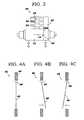
- FIGS. 4A-4Cshow schematic diagrams depicting the operation of the bypass valve shown in FIG. 2 and FIGS. 3A-3C in greater detail;
- FIG. 5shows an exploded view of a second embodiment of the bypass valve of the present invention.
- FIG. 6shows a schematic diagram depicting the operation of the bypass valve shown in FIG. 5 .
- FIGS. 1A-1Cshow a schematic representation of the operation of an electron beam lithography apparatus presently manufactured by International Business Machines Corporation under the model number EL 5 .
- EL 5One tool for advanced x-ray and chrome on glass mask making”, by Sturans et al. in J. Vac. Sci. Technol. B 16(6), Nov./Dec. 1998, pages 3164-3167 and in “Advanced Mask-Making with a Variable-Shaped Electron Beam”, by Pfeiffer et al. in Semiconductor Fabtech-15 th Edition, Winter,2002, pages 129-134.
- such an electron beam lithography apparatus 10includes a chamber 12 for holding a workpiece 14 in a known manner.
- the workpiece 14is typically a mask used in the manufacture of integrated circuits.
- the chamber 12includes and is enclosed by an outer wall 16 having an opening 18 therein.
- a second chamber 20has an electron beam column 22 mounted therein.
- the columnincludes a plurality of apertures 24 mounted therein for shaping the electron beam generated in the column 22 .
- the apertures 24are preferably made of cylindrical gold foil elements with the diameter of the cylinder defining the aperture. The inventors have found that such apertures are fragile and sensitive to contamination.
- the chamber 20includes and is enclosed by an outer wall 26 having portions 26 a and 26 b in common with the outer wall 16 of chamber 12 .
- the opening 18is in the common wall 26 a and is preferably a minimal size conductance limiting aperture.
- the opening 18is the only flow path between chambers 12 and 20 .
- the electron beam columnis mounted on the common wall 26 a and positioned to generate an electron beam 28 directed through the opening 18 at the workpiece 14 in chamber 12 .
- a pump 30is mounted on wall 16 of chamber 12 for creating a vacuum in chamber 12 .
- pump 12is capable of creating a high vacuum in chamber 12 of less than 5E-7 Torr.
- a pump 32is mounted on the wall 26 of chamber 20 for creating a high vacuum in chamber 20 equal to the vacuum in chamber 12 .
- a vent 34is mounted on the wall 16 of chamber 12 .
- a vent 36is mounted on the wall 26 of chamber 20 . The vents 34 and 36 are controlled, in a known manner, by a mechanism (not shown) external to the chambers 12 and 20 to vent the chambers 12 and 20 to gas at atmospheric pressure, thereby permitting gas to enter the chambers 12 and 20 and increasing the pressures in chambers 12 and 20 , respectively, until the chambers 12 and 20 are returned to atmospheric pressure.
- FIG. 1Cthe electron beam apparatus 10 is shown in a high vacuum condition, where any gas flow within the chambers 12 and 20 is a random, statistical process referred to as molecular flow.
- flow between chambers 12 and 20is independent of pressure because the pressures in chambers 12 and 20 are equal. Therefore, flow between chambers 12 and 20 can be minimized by the geometry of the conductance limiting aperture 18 , thus effectively minimizing any contamination of critical and sensitive components in the electron beam column 22 , such as the apertures 24 caused by process generated byproducts.
- FIG. 1Athe electron beam apparatus 10 is shown during a mode of operation in which the pumps 30 and 32 are operating to create a high vacuum condition within the chambers 12 and 20 .
- the gas in chambers 12 and 20initially behaves as a homogeneous fluid, then becomes turbulent and finally viscous as the pressures in chambers 12 and 20 decrease.
- the inventorshave observed that it can entrap and carry particulates. Since chambers 12 and 20 are of unequal volumes and since the pumps 30 and 32 operate independently, a pressure differential is likely to be created between chambers 12 and 20 . This pressure differential will case contaminated and potentially physically damaging gas to flow past the critical components in electron beam column 22 , such as apertures 24 .
- FIG. 1Ashows the condition where the pressure in chamber 12 is greater than the pressure in chamber 20 , thus causing gas from chamber 12 to flow through the aperture 18 and up the column 22 .
- FIG. 1Belectron beam apparatus 10 is shown during a mode of operation in which the vents 34 and 36 are opened to reduce the pressures in chambers 12 and 20 and return those pressures to atmospheric pressure. During this mode of operation, the gas in chambers 12 and 20 pass through the same phase changes, but in reverse order thus casing a similar contaminating flow condition.
- FIG. 1Bshows the condition where the pressure in chamber 20 exceeds the pressure in chamber 12 , thus causing gas from chamber 20 to flow down the column 22 and through aperture 18 .
- FIG. 2The electron beam apparatus of the present invention is shown in FIG. 2 with those elements that are common to the apparatus described in FIGS. 1A-1C being identified by the same reference numerals.
- An electron beam lithography apparatus 40has a balancing bypass valve 42 mounted in the common wall 26 b between chambers 12 and 20 .
- FIG. 3Ashows the operation of the apparatus 40 during a first mode of operation in which, for example, the pumps 30 and 32 are operating to create a high vacuum condition within the chambers 12 and 20 . In this mode of operation the pressure in chamber 12 exceeds the pressure in chamber 20 thus causing the bypass valve 42 to open in proportion to the pressure differential between chambers 12 and 20 and permit gas from chamber 12 to flow to chamber 20 and out of chamber 20 through pump 32 .
- FIG. 3Bshows the operation of the apparatus 40 during a second mode of operation in which, for example, the vents 34 and 36 are opened to the atmosphere thus increasing the pressure in chambers 12 and 20 until the pressure return to and equalizes at atmospheric pressure.
- the pressure in chamber 20exceeds the pressure in chamber 12 thus causing the bypass valve 42 to open in proportion to the pressure differential between chambers 20 and 12 and permit gas from chamber 20 to flow to chamber 12 .
- This flow pathalso bypasses the aperture 18 and correspondingly column 22 and apertures 24 thus minimizing contamination of those components.
- 3Cshows the operation of the apparatus 40 during a third mode of operation in which the apparatus 40 is operating under high vacuum, the pumps 30 and 32 are inoperative, the vents 34 and 36 are closed thereby sealing the chambers 12 and 20 from the environment and the pressures in chambers 12 and 20 are equal.
- the valve 42is closed, thus sealing the chamber 12 from the chamber 20 and preventing flow between chambers 12 and 20 and the apparatus 40 operates in the same manner as the apparatus 10 .
- the balancing bypass valve 42has a rectangular frame 44 mounted in the vertical common wall 26 b between chambers 12 and 20 .
- the bypass valve 42further includes a hinge 46 retained by the frame 44 and a rectangular valve gate 48 suspended from the hinge 46 and adapted to rotate thereabout.
- FIG. 4Athe pressures in chambers 12 and 20 are equal and the valve gate 48 is closed sealing chamber 12 from chamber 20 and thereby retaining any particulates generated during the processing of workpiece 14 from entering chamber 20 .
- FIG. 4Bcorresponds to the mode of operation depicted in FIG.
- FIG. 4Ccorresponds to the mode of operation depicted in FIG. 3B where the pressure in chamber 20 exceeds the pressure in chamber 12 thereby causing the valve gate 48 to rotate about the hinge 46 in proportion to the pressure differential between chambers 20 and 12 and permitting gas to flow from chamber 20 to chamber 12 .
- a second embodiment of the balancing bypass valve 42includes a rectangular frame 50 mounted in the vertical common wall 26 b between chambers 12 and 20 .
- a valve gate 52 made of a rectangular sheet of flexible materialis retained along at least a portion thereof at the top of the frame 50 by a clamping plate 54 and a dowel pin 56 which passes through a hole 58 in the gate 52 and a hole 60 in clamping plate 54 and seats by press fit in a hole 62 in offset portion 64 of frame 50 .
- the clamping plate 54is fastened to the offset portion 64 by a pair of socket head machine screws 66 adapted to pass through washers 68 and holes 70 in clamping plate 54 and to threadingly engage threaded boles 72 thereby clamping valve gate 52 to the top of frame 50 .
- the valve gate 50is preferably made of stainless steel approximately 50 microns thick.
- the valve gate 52is then suspended from the top 54 of the frame 50 and to open and close in response to pressure differentials between chambers 12 and 20 in the sane manner as the valve gate 48 . In FIG. 6 the valve gate 52 flexes to position 52 a in the mode of operation depicted in FIG. 3 A and flexes to position 52 b in the mode of operation depicted in FIG. 3 B.
- the present inventionprovides an electron beam lithography apparatus which minimizes contamination of the electron beam column components during pressure changes within the apparatus in a relatively simple and cost effective manner.
Landscapes
- Chemical & Material Sciences (AREA)
- Analytical Chemistry (AREA)
- Electron Beam Exposure (AREA)
- Exposure And Positioning Against Photoresist Photosensitive Materials (AREA)
Abstract
Description
Claims (17)
Priority Applications (1)
| Application Number | Priority Date | Filing Date | Title |
|---|---|---|---|
| US10/338,922US6724001B1 (en) | 2003-01-08 | 2003-01-08 | Electron beam lithography apparatus with self actuated vacuum bypass valve |
Applications Claiming Priority (1)
| Application Number | Priority Date | Filing Date | Title |
|---|---|---|---|
| US10/338,922US6724001B1 (en) | 2003-01-08 | 2003-01-08 | Electron beam lithography apparatus with self actuated vacuum bypass valve |
Publications (1)
| Publication Number | Publication Date |
|---|---|
| US6724001B1true US6724001B1 (en) | 2004-04-20 |
Family
ID=32069523
Family Applications (1)
| Application Number | Title | Priority Date | Filing Date |
|---|---|---|---|
| US10/338,922Expired - LifetimeUS6724001B1 (en) | 2003-01-08 | 2003-01-08 | Electron beam lithography apparatus with self actuated vacuum bypass valve |
Country Status (1)
| Country | Link |
|---|---|
| US (1) | US6724001B1 (en) |
Cited By (42)
| Publication number | Priority date | Publication date | Assignee | Title |
|---|---|---|---|---|
| US20150008334A1 (en)* | 2013-07-08 | 2015-01-08 | Carl Zeiss Microscopy, Llc | Charged particle beam system and method of operating a charged particle beam system |
| CN104282517A (en)* | 2013-07-08 | 2015-01-14 | 卡尔蔡司显微镜有限责任公司 | Charged particle beam system and method of operating a charged particle beam system |
| WO2016026674A1 (en)* | 2014-08-22 | 2016-02-25 | Arcam Ab | Enhanced additive manufacturing |
| US9664505B2 (en) | 2014-08-20 | 2017-05-30 | Arcam Ab | Energy beam position verification |
| US9676033B2 (en) | 2013-09-20 | 2017-06-13 | Arcam Ab | Method for additive manufacturing |
| US9676031B2 (en) | 2013-04-23 | 2017-06-13 | Arcam Ab | Method and apparatus for forming a three-dimensional article |
| US9713844B2 (en) | 2013-04-18 | 2017-07-25 | Arcam Ab | Method and apparatus for additive manufacturing |
| US9721755B2 (en) | 2015-01-21 | 2017-08-01 | Arcam Ab | Method and device for characterizing an electron beam |
| US9718129B2 (en) | 2012-12-17 | 2017-08-01 | Arcam Ab | Additive manufacturing method and apparatus |
| US9782933B2 (en) | 2008-01-03 | 2017-10-10 | Arcam Ab | Method and apparatus for producing three-dimensional objects |
| US9789541B2 (en) | 2014-03-07 | 2017-10-17 | Arcam Ab | Method for additive manufacturing of three-dimensional articles |
| US9789563B2 (en) | 2013-12-20 | 2017-10-17 | Arcam Ab | Method for additive manufacturing |
| US9802253B2 (en) | 2013-12-16 | 2017-10-31 | Arcam Ab | Additive manufacturing of three-dimensional articles |
| US9950367B2 (en) | 2014-04-02 | 2018-04-24 | Arcam Ab | Apparatus, method, and computer program product for fusing a workpiece |
| US10130993B2 (en) | 2013-12-18 | 2018-11-20 | Arcam Ab | Additive manufacturing of three-dimensional articles |
| US10144063B2 (en) | 2011-12-28 | 2018-12-04 | Arcam Ab | Method and apparatus for detecting defects in freeform fabrication |
| US10189086B2 (en) | 2011-12-28 | 2019-01-29 | Arcam Ab | Method and apparatus for manufacturing porous three-dimensional articles |
| US10369662B2 (en) | 2009-07-15 | 2019-08-06 | Arcam Ab | Method and apparatus for producing three-dimensional objects |
| US10434572B2 (en) | 2013-12-19 | 2019-10-08 | Arcam Ab | Method for additive manufacturing |
| US10525531B2 (en) | 2015-11-17 | 2020-01-07 | Arcam Ab | Additive manufacturing of three-dimensional articles |
| US10529070B2 (en) | 2017-11-10 | 2020-01-07 | Arcam Ab | Method and apparatus for detecting electron beam source filament wear |
| US10525547B2 (en) | 2016-06-01 | 2020-01-07 | Arcam Ab | Additive manufacturing of three-dimensional articles |
| US10549348B2 (en) | 2016-05-24 | 2020-02-04 | Arcam Ab | Method for additive manufacturing |
| US10583483B2 (en) | 2015-10-15 | 2020-03-10 | Arcam Ab | Method and apparatus for producing a three-dimensional article |
| US10610930B2 (en) | 2015-11-18 | 2020-04-07 | Arcam Ab | Additive manufacturing of three-dimensional articles |
| US10786865B2 (en) | 2014-12-15 | 2020-09-29 | Arcam Ab | Method for additive manufacturing |
| US10792757B2 (en) | 2016-10-25 | 2020-10-06 | Arcam Ab | Method and apparatus for additive manufacturing |
| US10800101B2 (en) | 2018-02-27 | 2020-10-13 | Arcam Ab | Compact build tank for an additive manufacturing apparatus |
| US10807187B2 (en) | 2015-09-24 | 2020-10-20 | Arcam Ab | X-ray calibration standard object |
| US10821721B2 (en) | 2017-11-27 | 2020-11-03 | Arcam Ab | Method for analysing a build layer |
| US10987752B2 (en) | 2016-12-21 | 2021-04-27 | Arcam Ab | Additive manufacturing of three-dimensional articles |
| US11014161B2 (en) | 2015-04-21 | 2021-05-25 | Arcam Ab | Method for additive manufacturing |
| US11059123B2 (en) | 2017-04-28 | 2021-07-13 | Arcam Ab | Additive manufacturing of three-dimensional articles |
| US11072117B2 (en) | 2017-11-27 | 2021-07-27 | Arcam Ab | Platform device |
| US11185926B2 (en) | 2017-09-29 | 2021-11-30 | Arcam Ab | Method and apparatus for additive manufacturing |
| US11247274B2 (en) | 2016-03-11 | 2022-02-15 | Arcam Ab | Method and apparatus for forming a three-dimensional article |
| US11267051B2 (en) | 2018-02-27 | 2022-03-08 | Arcam Ab | Build tank for an additive manufacturing apparatus |
| US11292062B2 (en) | 2017-05-30 | 2022-04-05 | Arcam Ab | Method and device for producing three-dimensional objects |
| US11325191B2 (en) | 2016-05-24 | 2022-05-10 | Arcam Ab | Method for additive manufacturing |
| US11400519B2 (en) | 2018-03-29 | 2022-08-02 | Arcam Ab | Method and device for distributing powder material |
| US11517975B2 (en) | 2017-12-22 | 2022-12-06 | Arcam Ab | Enhanced electron beam generation |
| US12350754B2 (en) | 2017-12-22 | 2025-07-08 | Arcam Ab | Electron beam source and the use of the same |
Citations (6)
| Publication number | Priority date | Publication date | Assignee | Title |
|---|---|---|---|---|
| US4298803A (en)* | 1979-01-19 | 1981-11-03 | Matsushita Electric Industrial Co., Ltd. | Process and apparatus for making fine-scale patterns |
| US4516030A (en)* | 1981-09-26 | 1985-05-07 | Fujitsu Limited | Scanning electron beam exposure system |
| US5092729A (en)* | 1989-10-27 | 1992-03-03 | Hitachi, Ltd. | Apparatus for transporting a wafer and a carrier used for the same |
| US5580419A (en)* | 1994-03-23 | 1996-12-03 | Trw Inc. | Process of making semiconductor device using focused ion beam for resistless in situ etching, deposition, and nucleation |
| US5914493A (en)* | 1997-02-21 | 1999-06-22 | Nikon Corporation | Charged-particle-beam exposure apparatus and methods with substrate-temperature control |
| US6573520B1 (en)* | 1999-03-26 | 2003-06-03 | Hitachi, Ltd. | Electron beam lithography system |
- 2003
- 2003-01-08USUS10/338,922patent/US6724001B1/ennot_activeExpired - Lifetime
Patent Citations (6)
| Publication number | Priority date | Publication date | Assignee | Title |
|---|---|---|---|---|
| US4298803A (en)* | 1979-01-19 | 1981-11-03 | Matsushita Electric Industrial Co., Ltd. | Process and apparatus for making fine-scale patterns |
| US4516030A (en)* | 1981-09-26 | 1985-05-07 | Fujitsu Limited | Scanning electron beam exposure system |
| US5092729A (en)* | 1989-10-27 | 1992-03-03 | Hitachi, Ltd. | Apparatus for transporting a wafer and a carrier used for the same |
| US5580419A (en)* | 1994-03-23 | 1996-12-03 | Trw Inc. | Process of making semiconductor device using focused ion beam for resistless in situ etching, deposition, and nucleation |
| US5914493A (en)* | 1997-02-21 | 1999-06-22 | Nikon Corporation | Charged-particle-beam exposure apparatus and methods with substrate-temperature control |
| US6573520B1 (en)* | 1999-03-26 | 2003-06-03 | Hitachi, Ltd. | Electron beam lithography system |
Non-Patent Citations (2)
| Title |
|---|
| Hans C. Pfeiffer & John Hartley, US IBM, "Advanced Mask-Making with a Variable-Shaped Electron Beam", pp. 129-134. |
| J. Vac. Sci. Technol. B 16(6), M.A. Sturans, et al. "ELS: One tool advanced x-ray and chrome on glass mask making", Nov./Dec. 1998, pp. 3164-3167. |
Cited By (79)
| Publication number | Priority date | Publication date | Assignee | Title |
|---|---|---|---|---|
| US9782933B2 (en) | 2008-01-03 | 2017-10-10 | Arcam Ab | Method and apparatus for producing three-dimensional objects |
| US10369662B2 (en) | 2009-07-15 | 2019-08-06 | Arcam Ab | Method and apparatus for producing three-dimensional objects |
| US11141790B2 (en) | 2011-12-28 | 2021-10-12 | Arcam Ab | Method and apparatus for manufacturing porous three-dimensional articles |
| US10144063B2 (en) | 2011-12-28 | 2018-12-04 | Arcam Ab | Method and apparatus for detecting defects in freeform fabrication |
| US10189086B2 (en) | 2011-12-28 | 2019-01-29 | Arcam Ab | Method and apparatus for manufacturing porous three-dimensional articles |
| US11161177B2 (en) | 2011-12-28 | 2021-11-02 | Arcam Ab | Method and apparatus for detecting defects in freeform fabrication |
| US10406599B2 (en) | 2012-12-17 | 2019-09-10 | Arcam Ab | Additive manufacturing method and apparatus |
| US9718129B2 (en) | 2012-12-17 | 2017-08-01 | Arcam Ab | Additive manufacturing method and apparatus |
| US9950366B2 (en) | 2013-04-18 | 2018-04-24 | Arcam Ab | Apparatus for additive manufacturing |
| US9713844B2 (en) | 2013-04-18 | 2017-07-25 | Arcam Ab | Method and apparatus for additive manufacturing |
| US9676031B2 (en) | 2013-04-23 | 2017-06-13 | Arcam Ab | Method and apparatus for forming a three-dimensional article |
| US9530612B2 (en) | 2013-07-08 | 2016-12-27 | Carl Zeiss Microscopy, Llc | Charged particle beam system and method of operating a charged particle beam system |
| US9530611B2 (en) | 2013-07-08 | 2016-12-27 | Carl Zeiss Microscopy, Llc | Charged particle beam system and method of operating a charged particle beam system |
| CN104282517A (en)* | 2013-07-08 | 2015-01-14 | 卡尔蔡司显微镜有限责任公司 | Charged particle beam system and method of operating a charged particle beam system |
| US9640364B2 (en)* | 2013-07-08 | 2017-05-02 | Carl Zeiss Microscopy, Llc | Charged particle beam system and method of operating a charged particle beam system |
| US9218934B2 (en) | 2013-07-08 | 2015-12-22 | Carl Zeiss Microscopy, Llc | Charged particle beam system and method of operating a charged particle beam system |
| US9627172B2 (en) | 2013-07-08 | 2017-04-18 | Carl Zeiss Microscopy, Llc | Charged particle beam system and method of operating a charged particle beam system |
| US9218935B2 (en)* | 2013-07-08 | 2015-12-22 | Carl Zeiss Microscopy, Llc | Charged particle beam system and method of operating a charged particle beam system |
| US9536699B2 (en) | 2013-07-08 | 2017-01-03 | Carl Zeiss Microscopy, Llc | Charged particle beam system and method of operating a charged particle beam system |
| US20160104598A1 (en)* | 2013-07-08 | 2016-04-14 | Carl Zeiss Microscopy, Llc | Charged Particle Beam System and Method of Operating a Charged Particle Beam System |
| CN104282517B (en)* | 2013-07-08 | 2018-02-16 | 卡尔蔡司显微镜有限责任公司 | The method of charged particle beam system and operation charged particle beam system |
| US20150008334A1 (en)* | 2013-07-08 | 2015-01-08 | Carl Zeiss Microscopy, Llc | Charged particle beam system and method of operating a charged particle beam system |
| US10814392B2 (en) | 2013-09-20 | 2020-10-27 | Arcam Ab | Apparatus for additive manufacturing |
| US10814393B2 (en) | 2013-09-20 | 2020-10-27 | Arcam Ab | Apparatus for additive manufacturing |
| US9676032B2 (en) | 2013-09-20 | 2017-06-13 | Arcam Ab | Method for additive manufacturing |
| US9676033B2 (en) | 2013-09-20 | 2017-06-13 | Arcam Ab | Method for additive manufacturing |
| US9802253B2 (en) | 2013-12-16 | 2017-10-31 | Arcam Ab | Additive manufacturing of three-dimensional articles |
| US10099289B2 (en) | 2013-12-16 | 2018-10-16 | Arcam Ab | Additive manufacturing of three-dimensional articles |
| US9919361B2 (en) | 2013-12-16 | 2018-03-20 | Arcam Ab | Additive manufacturing of three-dimensional articles |
| US10974448B2 (en) | 2013-12-18 | 2021-04-13 | Arcam Ab | Additive manufacturing of three-dimensional articles |
| US10130993B2 (en) | 2013-12-18 | 2018-11-20 | Arcam Ab | Additive manufacturing of three-dimensional articles |
| US10434572B2 (en) | 2013-12-19 | 2019-10-08 | Arcam Ab | Method for additive manufacturing |
| US11517964B2 (en) | 2013-12-19 | 2022-12-06 | Arcam Ab | Method for additive manufacturing |
| US9789563B2 (en) | 2013-12-20 | 2017-10-17 | Arcam Ab | Method for additive manufacturing |
| US10071424B2 (en) | 2014-03-07 | 2018-09-11 | Arcam Ab | Computer program products configured for additive manufacturing of three-dimensional articles |
| US9789541B2 (en) | 2014-03-07 | 2017-10-17 | Arcam Ab | Method for additive manufacturing of three-dimensional articles |
| US11084098B2 (en) | 2014-04-02 | 2021-08-10 | Arcam Ab | Apparatus for fusing a workpiece |
| US9950367B2 (en) | 2014-04-02 | 2018-04-24 | Arcam Ab | Apparatus, method, and computer program product for fusing a workpiece |
| US10071423B2 (en) | 2014-04-02 | 2018-09-11 | Arcam Ab | Apparatus, method, and computer program product for fusing a workpiece |
| US10058921B2 (en) | 2014-04-02 | 2018-08-28 | Arcam Ab | Apparatus, method, and computer program product for fusing a workpiece |
| US10821517B2 (en) | 2014-04-02 | 2020-11-03 | Arcam Ab | Apparatus, method, and computer program product for fusing a workpiece |
| US9897513B2 (en) | 2014-08-20 | 2018-02-20 | Arcam Ab | Energy beam size verification |
| US9915583B2 (en) | 2014-08-20 | 2018-03-13 | Arcam Ab | Energy beam position verification |
| US9664505B2 (en) | 2014-08-20 | 2017-05-30 | Arcam Ab | Energy beam position verification |
| US9664504B2 (en) | 2014-08-20 | 2017-05-30 | Arcam Ab | Energy beam size verification |
| WO2016026674A1 (en)* | 2014-08-22 | 2016-02-25 | Arcam Ab | Enhanced additive manufacturing |
| US12036730B2 (en) | 2014-12-15 | 2024-07-16 | Arcam Ab | Method for additive manufacturing |
| US10786865B2 (en) | 2014-12-15 | 2020-09-29 | Arcam Ab | Method for additive manufacturing |
| US10586683B2 (en) | 2015-01-21 | 2020-03-10 | Arcam Ab | Method and device for characterizing an electron beam |
| US9721755B2 (en) | 2015-01-21 | 2017-08-01 | Arcam Ab | Method and device for characterizing an electron beam |
| US12036731B2 (en) | 2015-04-21 | 2024-07-16 | Arcam Ab | Method for additive manufacturing |
| US11014161B2 (en) | 2015-04-21 | 2021-05-25 | Arcam Ab | Method for additive manufacturing |
| US11806800B2 (en) | 2015-09-24 | 2023-11-07 | Arcam Ab | X-ray calibration standard object |
| US10807187B2 (en) | 2015-09-24 | 2020-10-20 | Arcam Ab | X-ray calibration standard object |
| US10583483B2 (en) | 2015-10-15 | 2020-03-10 | Arcam Ab | Method and apparatus for producing a three-dimensional article |
| US11571748B2 (en) | 2015-10-15 | 2023-02-07 | Arcam Ab | Method and apparatus for producing a three-dimensional article |
| US10525531B2 (en) | 2015-11-17 | 2020-01-07 | Arcam Ab | Additive manufacturing of three-dimensional articles |
| US10610930B2 (en) | 2015-11-18 | 2020-04-07 | Arcam Ab | Additive manufacturing of three-dimensional articles |
| US11623282B2 (en) | 2015-11-18 | 2023-04-11 | Arcam Ab | Additive manufacturing of three-dimensional articles |
| US11247274B2 (en) | 2016-03-11 | 2022-02-15 | Arcam Ab | Method and apparatus for forming a three-dimensional article |
| US10549348B2 (en) | 2016-05-24 | 2020-02-04 | Arcam Ab | Method for additive manufacturing |
| US11325191B2 (en) | 2016-05-24 | 2022-05-10 | Arcam Ab | Method for additive manufacturing |
| US10525547B2 (en) | 2016-06-01 | 2020-01-07 | Arcam Ab | Additive manufacturing of three-dimensional articles |
| US10792757B2 (en) | 2016-10-25 | 2020-10-06 | Arcam Ab | Method and apparatus for additive manufacturing |
| US10987752B2 (en) | 2016-12-21 | 2021-04-27 | Arcam Ab | Additive manufacturing of three-dimensional articles |
| US11059123B2 (en) | 2017-04-28 | 2021-07-13 | Arcam Ab | Additive manufacturing of three-dimensional articles |
| US11292062B2 (en) | 2017-05-30 | 2022-04-05 | Arcam Ab | Method and device for producing three-dimensional objects |
| US11185926B2 (en) | 2017-09-29 | 2021-11-30 | Arcam Ab | Method and apparatus for additive manufacturing |
| US11993008B2 (en) | 2017-09-29 | 2024-05-28 | Arcam Ab | Method and apparatus for additive manufacturing |
| US10529070B2 (en) | 2017-11-10 | 2020-01-07 | Arcam Ab | Method and apparatus for detecting electron beam source filament wear |
| US10821721B2 (en) | 2017-11-27 | 2020-11-03 | Arcam Ab | Method for analysing a build layer |
| US11072117B2 (en) | 2017-11-27 | 2021-07-27 | Arcam Ab | Platform device |
| US11517975B2 (en) | 2017-12-22 | 2022-12-06 | Arcam Ab | Enhanced electron beam generation |
| US12350754B2 (en) | 2017-12-22 | 2025-07-08 | Arcam Ab | Electron beam source and the use of the same |
| US11267051B2 (en) | 2018-02-27 | 2022-03-08 | Arcam Ab | Build tank for an additive manufacturing apparatus |
| US11458682B2 (en) | 2018-02-27 | 2022-10-04 | Arcam Ab | Compact build tank for an additive manufacturing apparatus |
| US10800101B2 (en) | 2018-02-27 | 2020-10-13 | Arcam Ab | Compact build tank for an additive manufacturing apparatus |
| US11724316B2 (en) | 2018-03-29 | 2023-08-15 | Arcam Ab | Method and device for distributing powder material |
| US11400519B2 (en) | 2018-03-29 | 2022-08-02 | Arcam Ab | Method and device for distributing powder material |
Similar Documents
| Publication | Publication Date | Title |
|---|---|---|
| US6724001B1 (en) | Electron beam lithography apparatus with self actuated vacuum bypass valve | |
| TWI363152B (en) | Slit valve | |
| JP2766935B2 (en) | X-ray exposure equipment | |
| JPH054666A (en) | Vacuum cassette having air vent hole for semiconductor wafer | |
| US11054738B2 (en) | Pellicle | |
| US7927969B2 (en) | Cleaning of photolithography masks | |
| JP2001102281A (en) | Load lock chamber, chamber, semiconductor manufacturing apparatus and device manufacturing method | |
| JP3036873B2 (en) | Blow-out door for super clean surrounding container | |
| JP3817546B2 (en) | Electron beam lithography apparatus with a self-actuated vacuum bypass valve | |
| JP4446933B2 (en) | Transport of lithographic apparatus and patterning device | |
| US20040263819A1 (en) | Airtight processing apparatus, airtight processing method, and electron beam processing apparatus | |
| JP2005115389A (en) | Method and system for active purging of pellicle volume | |
| CN114280894B (en) | System and method for controlling and monitoring air pressure of photoetching machine and photoetching machine | |
| CN101166682A (en) | Substrate container with pressure equalization | |
| JP2004228562A (en) | Load lock purge method and its equipment | |
| CN100565345C (en) | The manufacture method of flat plate printing apparatus and equipment | |
| US20060033905A1 (en) | Pellicle-reticle methods with reduced haze or wrinkle formation | |
| JP2623127B2 (en) | X-ray exposure equipment | |
| JP2001053477A (en) | Case opening and closing device | |
| US20250164899A1 (en) | Apparatuses and methods for reducing particle contamination of wafers during transfer | |
| US20240006202A1 (en) | Apparatuses and methods for reducing particle contamination of wafers during transfer | |
| US7248340B2 (en) | Lithographic apparatus and patterning device transport | |
| JPS5812700B2 (en) | electron beam equipment | |
| JPH01225118A (en) | X-ray exposure device | |
| EP0501278A1 (en) | Method to produce masking |
Legal Events
| Date | Code | Title | Description |
|---|---|---|---|
| AS | Assignment | Owner name:INTERNATIONAL BUSINESS MACHINES CORPORATION, NEW Y Free format text:ASSIGNMENT OF ASSIGNORS INTEREST;ASSIGNORS:PINCKNEY, DAVID J.;KENDALL, RODNEY A.;REEL/FRAME:013657/0239 Effective date:20021220 | |
| FEPP | Fee payment procedure | Free format text:PAYOR NUMBER ASSIGNED (ORIGINAL EVENT CODE: ASPN); ENTITY STATUS OF PATENT OWNER: LARGE ENTITY | |
| STCF | Information on status: patent grant | Free format text:PATENTED CASE | |
| FPAY | Fee payment | Year of fee payment:4 | |
| FPAY | Fee payment | Year of fee payment:8 | |
| AS | Assignment | Owner name:GLOBALFOUNDRIES U.S. 2 LLC, NEW YORK Free format text:ASSIGNMENT OF ASSIGNORS INTEREST;ASSIGNOR:INTERNATIONAL BUSINESS MACHINES CORPORATION;REEL/FRAME:036550/0001 Effective date:20150629 | |
| AS | Assignment | Owner name:GLOBALFOUNDRIES INC., CAYMAN ISLANDS Free format text:ASSIGNMENT OF ASSIGNORS INTEREST;ASSIGNORS:GLOBALFOUNDRIES U.S. 2 LLC;GLOBALFOUNDRIES U.S. INC.;REEL/FRAME:036779/0001 Effective date:20150910 | |
| FPAY | Fee payment | Year of fee payment:12 | |
| AS | Assignment | Owner name:WILMINGTON TRUST, NATIONAL ASSOCIATION, DELAWARE Free format text:SECURITY AGREEMENT;ASSIGNOR:GLOBALFOUNDRIES INC.;REEL/FRAME:049490/0001 Effective date:20181127 | |
| AS | Assignment | Owner name:GLOBALFOUNDRIES U.S. INC., CALIFORNIA Free format text:ASSIGNMENT OF ASSIGNORS INTEREST;ASSIGNOR:GLOBALFOUNDRIES INC.;REEL/FRAME:054633/0001 Effective date:20201022 | |
| AS | Assignment | Owner name:GLOBALFOUNDRIES INC., CAYMAN ISLANDS Free format text:RELEASE BY SECURED PARTY;ASSIGNOR:WILMINGTON TRUST, NATIONAL ASSOCIATION;REEL/FRAME:054636/0001 Effective date:20201117 | |
| AS | Assignment | Owner name:GLOBALFOUNDRIES U.S. INC., NEW YORK Free format text:RELEASE BY SECURED PARTY;ASSIGNOR:WILMINGTON TRUST, NATIONAL ASSOCIATION;REEL/FRAME:056987/0001 Effective date:20201117 |