US6721149B1 - Tunneling magnetoresistance spin-valve read sensor with LaNiO3 spacer - Google Patents
Tunneling magnetoresistance spin-valve read sensor with LaNiO3 spacerDownload PDFInfo
- Publication number
- US6721149B1 US6721149B1US09/502,370US50237000AUS6721149B1US 6721149 B1US6721149 B1US 6721149B1US 50237000 AUS50237000 AUS 50237000AUS 6721149 B1US6721149 B1US 6721149B1
- Authority
- US
- United States
- Prior art keywords
- layer
- pinned
- pinned layer
- magnetoresistive sensor
- insulating spacer
- Prior art date
- Legal status (The legal status is an assumption and is not a legal conclusion. Google has not performed a legal analysis and makes no representation as to the accuracy of the status listed.)
- Expired - Lifetime
Links
Images


Classifications
- G—PHYSICS
- G01—MEASURING; TESTING
- G01R—MEASURING ELECTRIC VARIABLES; MEASURING MAGNETIC VARIABLES
- G01R33/00—Arrangements or instruments for measuring magnetic variables
- G01R33/02—Measuring direction or magnitude of magnetic fields or magnetic flux
- G01R33/06—Measuring direction or magnitude of magnetic fields or magnetic flux using galvano-magnetic devices
- G01R33/09—Magnetoresistive devices
- G01R33/093—Magnetoresistive devices using multilayer structures, e.g. giant magnetoresistance sensors
- B—PERFORMING OPERATIONS; TRANSPORTING
- B82—NANOTECHNOLOGY
- B82Y—SPECIFIC USES OR APPLICATIONS OF NANOSTRUCTURES; MEASUREMENT OR ANALYSIS OF NANOSTRUCTURES; MANUFACTURE OR TREATMENT OF NANOSTRUCTURES
- B82Y10/00—Nanotechnology for information processing, storage or transmission, e.g. quantum computing or single electron logic
- B—PERFORMING OPERATIONS; TRANSPORTING
- B82—NANOTECHNOLOGY
- B82Y—SPECIFIC USES OR APPLICATIONS OF NANOSTRUCTURES; MEASUREMENT OR ANALYSIS OF NANOSTRUCTURES; MANUFACTURE OR TREATMENT OF NANOSTRUCTURES
- B82Y25/00—Nanomagnetism, e.g. magnetoimpedance, anisotropic magnetoresistance, giant magnetoresistance or tunneling magnetoresistance
- G—PHYSICS
- G11—INFORMATION STORAGE
- G11B—INFORMATION STORAGE BASED ON RELATIVE MOVEMENT BETWEEN RECORD CARRIER AND TRANSDUCER
- G11B5/00—Recording by magnetisation or demagnetisation of a record carrier; Reproducing by magnetic means; Record carriers therefor
- G11B5/127—Structure or manufacture of heads, e.g. inductive
- G11B5/33—Structure or manufacture of flux-sensitive heads, i.e. for reproduction only; Combination of such heads with means for recording or erasing only
- G11B5/39—Structure or manufacture of flux-sensitive heads, i.e. for reproduction only; Combination of such heads with means for recording or erasing only using magneto-resistive devices or effects
- G11B5/3903—Structure or manufacture of flux-sensitive heads, i.e. for reproduction only; Combination of such heads with means for recording or erasing only using magneto-resistive devices or effects using magnetic thin film layers or their effects, the films being part of integrated structures
- G11B5/3906—Details related to the use of magnetic thin film layers or to their effects
- G11B5/3909—Arrangements using a magnetic tunnel junction
- G—PHYSICS
- G11—INFORMATION STORAGE
- G11B—INFORMATION STORAGE BASED ON RELATIVE MOVEMENT BETWEEN RECORD CARRIER AND TRANSDUCER
- G11B5/00—Recording by magnetisation or demagnetisation of a record carrier; Reproducing by magnetic means; Record carriers therefor
- G11B5/127—Structure or manufacture of heads, e.g. inductive
- G11B5/31—Structure or manufacture of heads, e.g. inductive using thin films
- G11B5/3109—Details
- G11B5/313—Disposition of layers
- G—PHYSICS
- G11—INFORMATION STORAGE
- G11B—INFORMATION STORAGE BASED ON RELATIVE MOVEMENT BETWEEN RECORD CARRIER AND TRANSDUCER
- G11B5/00—Recording by magnetisation or demagnetisation of a record carrier; Reproducing by magnetic means; Record carriers therefor
- G11B5/127—Structure or manufacture of heads, e.g. inductive
- G11B5/31—Structure or manufacture of heads, e.g. inductive using thin films
- G11B5/3163—Fabrication methods or processes specially adapted for a particular head structure, e.g. using base layers for electroplating, using functional layers for masking, using energy or particle beams for shaping the structure or modifying the properties of the basic layers
Definitions
- the present inventionrelates to magnetic recording technology, and more particularly to a tunneling magnetoresistive read head which is capable of being used in high density magnetic recording and can be easily manufactured.
- FIG. 1is a diagram of a conventional TMR junction 10 . Also depicted in FIG. 1 are leads 11 and 19 . Not depicted are conventional shields and gaps which would surround the conventional TMR junction 10 if the TMR junction 10 is used as a sensor.
- the conventional TMR junction 10includes a conventional antiferromagnetic (“AFM”) layer 12 , a conventional pinned layer 14 , a conventional insulating spacer layer 16 and a conventional free layer 18 .
- the conventional pinned layer 14 and conventional free layer 18are ferromagnetic.
- the conventional pinned layer 14has its magnetization fixed, or pinned, in place because the conventional pinned layer 14 is magnetically coupled to the conventional AFM layer 12 .
- the magnetization of the conventional free layer 18may be free to rotate in response to an external magnetic field.
- the conventional pinned layer 14is typically composed of Co, Fe, or Ni.
- the conventional free layer 18is typically composed of Co, Co 90 Fe 10 , or a bilayer of Co 90 Fe 10 and permalloy.
- the conventional insulating spacer layer 16is typically composed of aluminum oxide (Al 2 O 3 ).
- the conventional TMR junction 10For the conventional TMR junction 10 to function, current is driven between the leads 11 and 19 , perpendicular to the plane of the layers 12 , 14 , 16 and 18 of the conventional TMR junction 10 .
- the MR effect in the conventional TMR junction 10is believed to be due to spin polarized tunneling of electrons between the conventional free layer 18 and the conventional pinned layer 14 .
- the resistance of the conventional TMR junction 10is minimized or maximized.
- the bias point for the TMR junction 10is set.
- the magnetoresistance, MR, of a MR sensoris the difference between the maximum and minimum resistances of the MR sensor.
- the MR ratio of the MR sensoris typically called ⁇ R/R, and is typically given as a percent.
- the intrinsic magnetoresistance of such a conventional TMR junction 10is approximately seventeen percent.
- TMR junctionssuch as the conventional TMR junction 10
- TMR junctionsare of interest for MR sensors for high density recording applications.
- higher recording densitiesfor example over 40 gigabits (“Gb”) per square inch.
- Gbgigabits
- the signal from the read sensor for a given magnetic fieldis desired to be increased.
- One mechanism for increasing this signalwould be to use an MR sensor having an increased MR ratio.
- the conventional TMR junction 10is approximately seventeen percent, a higher MR ratio is desired.
- Some conventional TMR junctions 10have an increased MR ratio due to the resistance effect of the leads 11 and 19 .
- an MR ratio of up to forty percenthas been reported.
- the high MR ratio for such conventional TMR junctions 10is due to lead resistance.
- the resistance of the leads 11 and 19is much higher than the resistance of the conventional TMR junction itself of the conventional TMR sensor 10 , which is on the order of sixty ohms per micrometer squared. Consequently, the resistance of the combination of the TMR junction 10 and the leads 11 and 19 is high.
- FIG. 2Adepicts another conventional TMR junction 20 disclosed in “Inverse Tunnel Magnetoresistance in Co/SrTiO 3 /La 0.7 Sr 0.3 MnO 3 : New Ideas on Spin-Polarized Tunneling” J. M. De Maria, A. Barthelemy, A. Fert, J. P. Contour, R. Lyonnet, F. Montaigne, P. Seneor, and A. Vaures, Phys. Rev. Lett., Vol. 82, No. 21, 4288-4291 (1999). Also depicted in FIG. 1B are leads 21 and 29 , which are used to carry current to and from the conventional TRM junction 20 .
- the conventional TMR sensor 20includes an antiferromagnetic layer 22 .
- LSMOLa 0.7 Sr 0.3 MnO 3
- STOSrTiO 3
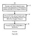
- FIG. 2Bdepicts a conventional method 40 for forming the conventional TMR junction 20 .
- the LSMO pinned layer 24is provided using pulsed laser deposition at seven hundred degrees Celsius and an oxygen pressure of three hundred and fifty millitorr, via step 42 .
- the STO insulating layer 26is then provided using pulsed laser deposition at seven hundred degrees Celsius and an oxygen pressure of three hundred and fifty millitorr, via step 44 .
- the conventional pinned layer 28 of Cois then provided using molecular beam epitaxy or sputtering, via step 46 .
- the conventional TMR junction 20utilizes the STO insulating layer 26 in order to improve the MR for the conventional TMR junction 20 . It is believed that d-shell electrons can tunnel more readily through the STO insulating layer 26 than through an insulating layer such as the aluminum oxide insulating spacer layer 16 used in the conventional TMR junction 10 . Ferromagnetic materials, such as Co, have d-shell electrons in their unfilled shell. Moreover, the magnetic properties of many ferromagnetic materials are dominated by the d-shell electrons. The STO insulating layer 26 more readily forms d electron bonds with the conventional free layer 28 at the interface between the STO insulating layer 26 and the conventional free layer 28 .
- the d-shell electrons from the conventional free layer 28can more readily tunnel through the STO insulating layer 26 .
- tunneling of spin polarized electronsis more likely to take place in the conventional TMR junction 20 than in the conventional TMR junction 10 , which has an insulating spacer layer 16 of aluminum oxide through which s-shell electrons are more likely to tunnel. Therefore, the MR ratio of the conventional TMR junction 20 is higher.
- the LSMO pinned layer 24is what is known as a half metallic ferromagnet.
- a half metallic ferromagnethas electrons of only one spin type in its unfilled shells.
- the spin polarization of a materialis proportional to the number of spin up electrons in the material's unfilled shell minus the number of spin down electrons in the material's unfilled shell.
- the spin polarizationis typically expressed as a percentage.
- a half metallic ferromagnethas a spin polarization of one hundred percent.
- the MR ratio for a TMR junctionis 2*P 1 *P 2 /(1+P 1 *P 2 ), where P 1 and P 2 are the spin polarizations of the free layer and the pinned layer, respectively.
- the MR ratiois increased because P 2 is one hundred percent (or one, expressed as a fraction).
- the MR ratio for the conventional TMR junction 20is increased, and has been observed to reach approximately fifty percent.
- the conventional TMR junction 20has improved MR, one of ordinary skill in the art will readily realize that the TMR junction 20 may not be suitable for use as a sensor in a MR head.
- the TMR junction 20is formed using very high temperature and energy deposition techniques for both the LSMO pinned layer 24 and the STO insulating spacer layer 26 .
- the TMR junction 20itself and other structures which may be used in a MR head, such as shields or leads, may be damaged.
- the performance of the TMR junction 20is adversely affected. Because the LSMO pinned layer 24 is deposited using high temperature laser ablation, the conventional AFM layer 22 may be heated during deposition of the LSMO pinned layer 24 .
- Heating of the AFM layer 22may change the crystal structure of the AFM layer 22 , thereby changing the magnetic properties of the AFM layer 22 . Consequently, the AFM layer 22 will be less able to pin the magnetization of the LSMO pinned layer 24 in the desired direction.
- the TMR junction 20may not, therefore, function as desired.
- other structuressuch as the shields or (not shown in FIGS. 1, 2 A or 2 B) or lead 21 may be damaged by heating during deposition of the LSMO pinned layer 24 or the STO insulating layer 26 . If the shields are damaged, the shields may not adequately perform their desired function, screening the TMR junction 20 from the magnetic due to bits which are not being read.
- the TMR junction 20may read spurious magnetic fields as part of the magnetic field of the bit desired to be read. Performance of the TMR junction 20 may, therefore, be adversely affected because of the deposition of the LSMO pinned layer 24 and, to a lesser extent, the deposition of the STO insulating layer 26 .
- the present inventionprovides a method and system for providing a magnetoresistive sensor that reads data from a recording media.
- the method and systemcomprise providing an antiferromagnetic layer, providing a pinned layer without adversely affecting performance of the magnetoresistance sensor, providing a free layer, and providing an insulating spacer layer disposed between the pinned layer and the free layer.
- the pinned layeris magnetically coupled to the antiferromagnetic layer.
- the pinned layeris also a half metallic ferromagnet.
- the free layeris magnetic.
- the insulating spacer layeris sufficiently thin to allow tunneling of charge carriers between the pinned layer and the free layer. Furthermore, the insulating spacer layer allows for d-bonding between a portion of the free layer and a portion of the insulating spacer layer.
- the present inventionprovides a tunneling magnetoresistive sensor which has a high magnetoresistance and which can be fabricated using techniques which will not adversely affect the performance of the magnetoresistive sensor. Consequently, the MR head is capable of reading higher density recording media and fabricated using techniques similar to those currently used for conventional magnetoresistive heads.
- FIG. 1is a diagram of a conventional tunneling magnetoresistive junction.
- FIG. 2Ais a diagram of a second conventional tunneling magnetoresistive junction.
- FIG. 2Bis a flow chart depicting a conventional method for providing the second conventional tunneling magnetoresistive junction.
- FIG. 3Ais a diagram of one embodiment of a tunneling magnetoresistive sensor in accordance with the present invention.
- FIG. 3Bis a diagram of a second embodiment of a tunneling magnetoresistive sensor in accordance with the present invention.
- FIG. 4is a diagram of a portion of one embodiment of the magnetoresistive head in accordance with the present invention.
- FIG. 5Ais a flow chart depicting one embodiment of a method for providing a tunneling magnetbresistive sensor in accordance with the present invention.
- FIG. 5Bis a flow chart depicting one embodiment of a method for providing a tunneling magnetoresistive as incorporated into a magnetoresistive head in accordance with the present invention.
- the present inventionrelates to an improvement in magnetoresistive heads.
- the following descriptionis presented to enable one of ordinary skill in the art to make and use the invention and is provided in the context of a patent application and its requirements.
- Various modifications to the preferred embodimentwill be readily apparent to those skilled in the art and the generic principles herein may be applied to other embodiments.
- the present inventionis not intended to be limited to the embodiment shown, but is to be accorded the widest scope consistent with the principles and features described herein.
- Tunneling magnetoresistive (“TMR”) junctionsare of increasing interest for use as magnetoresistive (“MR”) sensors in MR heads.
- TMR junctionsrely on tunneling of spin polarized electrons through an insulating layer between two magnetic layers, a conventional free layer and a conventional pinned layer.
- ⁇ R/RIn order to increase the MR ratio, ⁇ R/R, for conventional TMR junctions, two proposals have been made. The first uses an increased resistance in the leads carrying current to and from the conventional TMR junction in order to increase the MR ratio. However, this results in a very high resistance for the combination of the conventional TMR junction and the leads. Consequently, an MR head built with such a combination would have a slow response time and, therefore, a low data rate. These properties are undesirable.
- a second conventional TMR junctionutilizes a La 0.7 Sr 0.3 MnO 3 (“LSMO”) pinned layer and a SrTiO 3 (“STO”) insulating spacer layer. Because of the properties of the LSMO pinned layer and the STO insulating spacer layer, the MR ratio for the second conventional TMR junction is increased. However, one of ordinary skill in the art will readily recognize that the conventional techniques used to provide the second conventional TMR junction can adversely affect the performance of the TMR junction when used as a MR sensor. In particular, high temperature laser ablation is used to provide the LSMO pinned layer and the STO insulating spacer layer.
- the high temperature used in providing, for example, the LSMO spacer layercan damage portions of the sensor or the head, such as AFM layer of the conventional TMR junction, and possibly the shield or leads.
- the second TMR junctionmay not function as desired in the MR head.
- the second conventional TMR sensormay not be suitable for use as a MR sensor.
- the present inventionprovides a method and system for providing a magnetoresistive sensor that reads data from a recording media.
- the method and systemcomprise providing an antiferromagnetic layer, providing a pinned layer without adversely affecting performance of the magnetoresistance sensor, providing a free layer, and providing an insulating spacer layer disposed between the pinned layer and the free layer.
- the pinned layeris magnetically coupled to the antiferromagnetic layer.
- the pinned layeris also a half metallic ferromagnet.
- the free layeris magnetic.
- the insulating spacer layeris sufficiently thin to allow tunneling of charge carriers between the pinned layer and the free layer.
- the insulating spacer layerallows for d-bonding between a portion of the free layer and a portion of the insulating spacer layer.
- the insulating spacer layeralso preferably allows for d-bonding between a portion of the insulating spacer layer and a portion of the pinned layer.
- the present inventionwill be described in terms of particular materials used, a particular head, and a particular configuration of the TMR sensor. However, one of ordinary skill in the art will readily recognize that this method and system will operate effectively for other materials and other configurations of the TMR sensor of the MR head consistent with the present invention.
- the present inventionis consistent with the use of a spin valve, a dual spin valve, a synthetic spin valve, or other magnetoresistive sensor.
- the present inventioncan be used in a simple read head, a merged head, or another head which utilizes a TMR sensor as described herein.
- the TMR sensor 100includes an antiferromagnetic (AFM) layer 102 , a pinned layer 104 , an insulating spacer layer 106 and a free layer 108 .
- the free layer 108is preferably Co, Co 90 Fe 10 or a bilayer of Co 90 Fe 10 and permalloy.
- the pinned layer 104is preferably a half metallic ferromagnet.
- the pinned layer 104is also composed of a material such that providing the pinned layer 104 for the TMR sensor 100 does not adversely affect the performance TMR sensor 100 .
- the pinned layer 104is a Heusler alloy NiMnSb.
- the pinned layer 104may include Fe 3 O 4 , CrO 2 , CoO 2 , CoS 2 , Nd 0.7 Sr 0.3 MnO 3 or another material which can be provided without adversely affecting the performance of the TMR sensor 100 .
- the insulating spacer layer 106is also provided in a manner which will not adversely affect the performance of the TMR sensor 100 .
- the insulating spacer layer 106sufficiently thin to allow tunneling of charge carriers between the pinned layer 104 and the free layer 108 during operation of the TMR sensor.
- the insulating spacer layer 106has a structure which allows for d-bonding between a portion of the free layer 108 and a portion of the insulating spacer layer 106 .
- the insulating spacer layer 106is preferably an STO layer, which is known to allow for d-shell bonding between the Ti in the STO and at least Co.
- the insulating spacer layermay include LaNiO 3 , which also allows for d-shell bonding between the Ni in the LaNiO 3 and Co.
- the insulating spacer layer 106also allows for d-shell bonding between a portion of the insulating spacer layer 106 and the pinned layer 104 .
- antiferromagnetic layer 102is approximately fifty to five hundred Angstroms thick
- the pinned layer 104is approximately ten to fifty Angstroms thick
- the insulating spacer layer 106is five to twenty Angstroms thick
- the free layer 108is ten to one hundred Angstroms thick.
- the tunneling MR ratio for a TMR junctionis proportional to 2*P 1 P 2 /(1+P 1 *P 2 ), where P 1 and P 2 are the spin polarizations of the free layer 108 and the pinned layer 104 , respectively.
- P 1 and P 2are the spin polarizations of the free layer 108 and the pinned layer 104 , respectively.
- the tunneling MR ratio for the TMR sensor 100is increased.
- the MR for the TMR sensor 100is also increased above that for a conventional TMR sensor for which s-shell electrons are more likely to tunnel. It is believed that the tunneling MR for the TMR sensor 100 may be capable of being fifty percent or more at room temperature.
- the pinned layer 104can be provided without adversely affecting the performance of the TMR sensor 100 .
- the AFM layer 102may not be damaged when the pinned layer 104 is provided.
- other portions of the TMR sensor 100 and other portions of the MR head (not shown)are not damaged when the pinned layer 104 is provided. As a result, the TMR sensor 100 may be capable of providing better performance.
- FIG. 3Bdepicts another embodiment of the TMR sensor 100 ′.
- the pinned layer 104 ′, the insulating spacer layer 106 ′ and the free layer 108 ′are substantially the same as the pinned layer 104 , the insulating spacer layer 106 and the free layer 108 shown in FIG. 3 A.
- the free layer 108 ′is preferably Co, Co 90 Fe 10 or a bilayer of Co 90 Fe 10 and permalloy.
- the pinned layer 104 ′is preferably a half metallic ferromagnet.
- the pinned layer 104 ′is also composed of a material such that providing the pinned layer 104 ′ for the TMR sensor 100 ′ does not adversely affect the performance TMR sensor 100 ′.
- the pinned layer. 104 ′is a Heusler alloy NiMnSb.
- the pinned layer 104may include Fe 3 O 4 , CrO 2 , CoO 2 , CoS 2 , Nd 0.7 Sr 0.3 MnO 3 or another material which can be provided without adversely affecting the, performance of the TMR sensor 100 ′.
- the insulating spacer layer 106 ′is also provided in a manner which will not adversely affect the performance of the TMR sensor 100 ′.
- antiferromagnetic layer 102 ′is approximately fifty to five hundred Angstroms thick
- the pinned layer 104 ′is approximately ten to fifty Angstroms thick
- the insulating spacer layer 106 ′is five to twenty Angstroms thick
- the free layer 108 ′is ten to one hundred Angstroms thick.
- the TMR sensor 100 ′thus can have a large MR and can function to provide a larger signal in response to the magnetic field from a bit (not shown).
- the insulating spacer layer 106 ′allows for tunneling of spin polarized electrons and allows for d-shell bonding at the interface between the spacer layer 106 ′ and the free layer 108 ′ and because, in a preferred embodiment, the insulating spacer layer 106 ′ also allows for d-shell bonding between a portion of the insulating spacer layer 106 ′ and the pinned layer 104 ′.
- the advantagescan also be realized because the pinned layer 104 ′ is a half metallic ferromagnet and because the pinned layer 104 ′ can be provided without adversely affecting the performance of the TMR sensor 100 ′.
- the advantagesare also realized because the pinned layer 104 ′ does not adversely affect other portions of the TMR sensor 100 ′, such as the synthetic AFM layer 102 ′, or other portions of the MR head (not shown) in which the TMR sensor 100 ′ may be used.
- the TMR sensor 100 ′can provide many of the advantages of the TMR sensor 100 .
- the TMR sensor 100 ′also includes a synthetic AFM layer 102 ′.
- the synthetic AFM layer 102 ′is used to pin the magnetization of the pinned layer 104 ′.
- the synthetic AFM layer 102 ′preferably includes an AFM layer 110 , a magnetic layer 112 and a nonmagnetic layer 114 .
- the AFM layer 110aids in pinning the magnetization of the magnetic layer 112 in a desired direction.
- the nonmagnetic layer 114has a thickness that allows for antiferromagnetic coupling between the pinned layer 104 ′ and the magnetic layer 112 . This relatively strong antiferromagnetic coupling between the magnetic layer 112 and the pinned layer 104 ′ pins the magnetization of the pinned layer 104 ′ in the desired direction.
- the pinning of the magnetization of the pinned layer 104 ′may be more complete than for the pinned layer 104 of the TMR sensor 100 depicted in FIG. 3 A.
- the magnetic layer 112is preferably Co
- the nonmagnetic layeris preferably Ru
- the AFM layer 112is preferably PtMn.
- the pinned layer 104is preferably the Heusler alloy NiMnSb.
- a metallic pinned layer 104 ′is preferred because the antiferromagnetic coupling between the pinned layer 104 ′ and the magnetic layer 112 may be significantly more difficult to establish when the pinned layer 104 ′ is an insulator or oxide.
- FIG. 4depicts a portion of an MR head 120 which utilizes the TMR sensor 100 as a read sensor.
- the MR head 120could be part of a merged head which also includes a write head (not shown).
- the MR head 120is depicted as including the TMR sensor 100 , the TMR sensor 100 ′ could be included in the MR head 120 in lieu of the TMR sensor 100 .
- the MR head 120includes first and second shields 122 and 132 , respectively, as well as first and second gaps 124 and 130 , respectively.
- the first and second shields 122 and 132shield the TMR sensor 100 from magnetic fields due to adjacent bits (not shown) which are not desired to be read.
- the TMR sensor 100will be exposed primarily to the magnetic field of the bit which is to be read.
- the first and second gaps 124 and 130are insulators that insulate the TMR sensor 100 from the shields 122 and 132 , respectively.
- the MR head 120also includes leads 126 and 128 .
- the leads 126 and 128are used to carry current to and from the TMR sensor 100 .
- the MR head 120could include other components which are not shown, such as a seed layer and capping layer for the TMR sensor 100 or 100 ′.
- the MR head 120may be capable of reading higher density recording media.
- the TMR sensor 100 and 100 ′have a higher MR ratio than a conventional TMR sensor and is not damaged during formation of the TMR sensor 100 and 100 ′, respectively.
- portions of the MR head 120such as the shield 122 or lead 124 are not damaged during formation of the pinned layer 104 and 104 ′ of the TMR sensor 100 and 100 ′, respectively. It is believed that the high MR ratio may allow the MR head 120 to read at densities of 40 Gb/square inch and higher.
- FIG. 5Adepicts one embodiment of a method 200 for providing the TMR sensor 100 or 100 ′ in accordance with the present invention.
- the AFM layer 102 or synthetic AFM 102 ′is provided, via step 202 .
- the pinned layer 104 or 104 ′is then provided such that the operation of the sensor 100 or 100 ′, respectively, is not adversely affected, via step 204 .
- the pinned layer 104 or 104 ′is sputtered or deposited using chemical vapor deposition (“CVD”).
- CVDchemical vapor deposition
- NiMnSb layermay be provided by sputtering the layer at a temperature of up to two hundred and fifty degrees Celsius. This temperature is comparable to temperatures already used to fabricate conventional commercial metallic spin valves.
- Deposition of the pinned layer 104 or 104 ′ under such conditionsprecludes damage to the TMR sensor 100 or 100 ′ as well as portions of the head 120 .
- a temperature of not more than four hundred degrees Celsiusis desired to be used to help prevent damage to the TMR sensor 100 and 100 ′, as well as to prevent damage to other portions of the head 120 .
- operation of the TMR sensor 100 or 100 ′is not adversely affected.
- the insulating layer 106 or 106 ′is then provided, via step 206 .
- the insulating layer 106 or 106 ′is also provided such that operation of the TMR sensor 100 and 100 ′ is not affected.
- sputtering of NiMnSb for the pinned layer 102 and 102 ′can be carried out at temperatures of up to two hundred and fifty degrees Celsius.
- the insulating layermay be deposited using CVD. These temperatures do not heat the AFM layer 102 or the synthetic AFM 102 ′ sufficiently to change the structure of the AFM layer 102 or the synthetic AFM 102 ′. Thus, it is preferred that the temperature not be over four hundred degrees Celsius.
- the magnetic properties of the AFM layer 102 and the synthetic AFM 102 ′remain unchanged during deposition of the pinned layer 104 and 104 ′, respectively, and the insulating layer 106 and 106 ′, respectively. Consequently, the AFM layer 102 or the synthetic AFM 102 ′ remains capable of pinning the magnetization of the pinned layer 104 and 104 ′, respectively, in the desired direction.
- FIG. 5Bdepicts another embodiment of a method 220 for providing a MR head, such as the MR head 120 , in accordance with the present invention.
- the first shield 122is provided, via step 222 .
- the first gap 124 and lead 126are provided, via steps 224 and 226 , respectively.
- the AFM layer 102 or synthetic AFM 102 ′is then provided, via step 228 . Note that a seed layer may be provided before the AFM layer 102 or synthetic AFM layer 102 ′ are provided. If the synthetic AFM layer 102 ′ is provided in step 228 , then step 228 preferably includes providing an AFM layer, providing a magnetic layer and providing a nonmagnetic layer.
- the pinned layer 104 or 104 ′is then provided, via step 230 .
- Step 230may include sputtering the pinned layer 104 or 104 ′ or providing the pinned layer 104 or 104 ′ by CVD.
- the pinned layer 104 or 104 ′is a Heusler allow of NiMnSb and is sputtered at a temperature of up to approximately two hundred and fifty degrees Celsius.
- the insulating spacer layer 106 or 106 ′is then provided, via step 232 .
- step 232includes providing a layer of SrTiO 3 using CVD. Thus, deposition of the insulating layer also does not adversely affect the performance of the TMR sensor 100 or 100 ′.
- the free layer 108 or 108 ′is then provided, via step 234 .
- the lead 128 , second gap 130 and second shield 132are then provided, via steps 236 , 238 and 240 , respectively.
- the TMR sensor 100 and 100 ′can be provided in the head 120 . Because the pinned layer 104 and 104 ′ is provided without adversely affecting the operation of the TMR sensor 100 and 100 ′, the TMR sensor 100 and 100 ′ can be used to read higher density recording media. For example, the pinned layer 104 and 104 ′, as well as the insulating layers 106 and 106 ′, can be provided without raising the temperature of the TMR sensor 100 or 100 ′ or the head 120 to high temperatures such as seven hundred degrees Celsius. As a result, the AFM layer 102 and the synthetic AFM 102 ′ retain the desired magnetic properties. Furthermore, structures, such as the shield 122 or lead 126 , may not be damaged or destroyed.
- the TMR sensor 100 and 100 ′can function as desired. Furthermore, the TMR sensor 100 and 100 ′ can have higher MR because of the use of a half metallic ferromagnet, or other material having a high spin polarization, and because the insulating spacer layer 106 and 106 ′, respectively, allows for improved tunneling of d-shell electrons.
Landscapes
- Engineering & Computer Science (AREA)
- Chemical & Material Sciences (AREA)
- Nanotechnology (AREA)
- Physics & Mathematics (AREA)
- Crystallography & Structural Chemistry (AREA)
- Manufacturing & Machinery (AREA)
- Condensed Matter Physics & Semiconductors (AREA)
- General Physics & Mathematics (AREA)
- Mathematical Physics (AREA)
- Theoretical Computer Science (AREA)
- Magnetic Heads (AREA)
- Hall/Mr Elements (AREA)
Abstract
Description
Claims (12)
Priority Applications (1)
| Application Number | Priority Date | Filing Date | Title |
|---|---|---|---|
| US09/502,370US6721149B1 (en) | 2000-02-11 | 2000-02-11 | Tunneling magnetoresistance spin-valve read sensor with LaNiO3 spacer |
Applications Claiming Priority (1)
| Application Number | Priority Date | Filing Date | Title |
|---|---|---|---|
| US09/502,370US6721149B1 (en) | 2000-02-11 | 2000-02-11 | Tunneling magnetoresistance spin-valve read sensor with LaNiO3 spacer |
Publications (1)
| Publication Number | Publication Date |
|---|---|
| US6721149B1true US6721149B1 (en) | 2004-04-13 |
Family
ID=32043546
Family Applications (1)
| Application Number | Title | Priority Date | Filing Date |
|---|---|---|---|
| US09/502,370Expired - LifetimeUS6721149B1 (en) | 2000-02-11 | 2000-02-11 | Tunneling magnetoresistance spin-valve read sensor with LaNiO3 spacer |
Country Status (1)
| Country | Link |
|---|---|
| US (1) | US6721149B1 (en) |
Cited By (144)
| Publication number | Priority date | Publication date | Assignee | Title |
|---|---|---|---|---|
| US20030011463A1 (en)* | 2001-06-22 | 2003-01-16 | Kabushiki Kaisha Toshiba | Magnetoresistive effect element, magnetic head and magnetic reproducing apparatus |
| US20030137785A1 (en)* | 2002-01-24 | 2003-07-24 | Alps Electric Co., Ltd. | Magnetic sensing element containing half-metallic alloy |
| US20030161079A1 (en)* | 2002-02-27 | 2003-08-28 | Hiromasa Takahashi | Magnetic head, and the magnetic read-write devices, and the magnetic memory with magnetic sensors |
| US20040101978A1 (en)* | 2002-11-25 | 2004-05-27 | Tsann Linn | Method of forming a barrier layer of a tunneling magnetoresistive sensor |
| US20050073778A1 (en)* | 2003-10-06 | 2005-04-07 | Alps Electric Co., Ltd. | Magnetic sensing element including magnetic layer composed of Heusler alloy disposed on underlayer having {111}-oriented fcc structure |
| US6958927B1 (en)* | 2002-10-09 | 2005-10-25 | Grandis Inc. | Magnetic element utilizing spin-transfer and half-metals and an MRAM device using the magnetic element |
| US20060067009A1 (en)* | 2004-09-27 | 2006-03-30 | Marie-Claire Cyrille | Read head having shaped read sensor-biasing layer junctions using partial milling and method of fabrication |
| US20070091675A1 (en)* | 2005-10-20 | 2007-04-26 | Seagate Technology Llc | Double bias for a magnetic reader |
| US20080068765A1 (en)* | 2001-06-22 | 2008-03-20 | Kabushiki Kaisha Toshiba | Magnetoresistive effect element, magnetic head and magnetic reproducing apparatus |
| US8766383B2 (en) | 2011-07-07 | 2014-07-01 | Samsung Electronics Co., Ltd. | Method and system for providing a magnetic junction using half metallic ferromagnets |
| US8830628B1 (en) | 2009-02-23 | 2014-09-09 | Western Digital (Fremont), Llc | Method and system for providing a perpendicular magnetic recording head |
| US8879207B1 (en) | 2011-12-20 | 2014-11-04 | Western Digital (Fremont), Llc | Method for providing a side shield for a magnetic recording transducer using an air bridge |
| US8883017B1 (en) | 2013-03-12 | 2014-11-11 | Western Digital (Fremont), Llc | Method and system for providing a read transducer having seamless interfaces |
| US8917581B1 (en) | 2013-12-18 | 2014-12-23 | Western Digital Technologies, Inc. | Self-anneal process for a near field transducer and chimney in a hard disk drive assembly |
| US8923102B1 (en) | 2013-07-16 | 2014-12-30 | Western Digital (Fremont), Llc | Optical grating coupling for interferometric waveguides in heat assisted magnetic recording heads |
| US8947985B1 (en) | 2013-07-16 | 2015-02-03 | Western Digital (Fremont), Llc | Heat assisted magnetic recording transducers having a recessed pole |
| US8953422B1 (en) | 2014-06-10 | 2015-02-10 | Western Digital (Fremont), Llc | Near field transducer using dielectric waveguide core with fine ridge feature |
| US8958272B1 (en) | 2014-06-10 | 2015-02-17 | Western Digital (Fremont), Llc | Interfering near field transducer for energy assisted magnetic recording |
| US8970988B1 (en) | 2013-12-31 | 2015-03-03 | Western Digital (Fremont), Llc | Electric gaps and method for making electric gaps for multiple sensor arrays |
| US8971160B1 (en) | 2013-12-19 | 2015-03-03 | Western Digital (Fremont), Llc | Near field transducer with high refractive index pin for heat assisted magnetic recording |
| US8976635B1 (en) | 2014-06-10 | 2015-03-10 | Western Digital (Fremont), Llc | Near field transducer driven by a transverse electric waveguide for energy assisted magnetic recording |
| US8980109B1 (en) | 2012-12-11 | 2015-03-17 | Western Digital (Fremont), Llc | Method for providing a magnetic recording transducer using a combined main pole and side shield CMP for a wraparound shield scheme |
| US8982508B1 (en) | 2011-10-31 | 2015-03-17 | Western Digital (Fremont), Llc | Method for providing a side shield for a magnetic recording transducer |
| US8984740B1 (en) | 2012-11-30 | 2015-03-24 | Western Digital (Fremont), Llc | Process for providing a magnetic recording transducer having a smooth magnetic seed layer |
| US8988825B1 (en) | 2014-02-28 | 2015-03-24 | Western Digital (Fremont, LLC | Method for fabricating a magnetic writer having half-side shields |
| US8988812B1 (en) | 2013-11-27 | 2015-03-24 | Western Digital (Fremont), Llc | Multi-sensor array configuration for a two-dimensional magnetic recording (TDMR) operation |
| US8995087B1 (en) | 2006-11-29 | 2015-03-31 | Western Digital (Fremont), Llc | Perpendicular magnetic recording write head having a wrap around shield |
| US8993217B1 (en) | 2013-04-04 | 2015-03-31 | Western Digital (Fremont), Llc | Double exposure technique for high resolution disk imaging |
| US9001628B1 (en) | 2013-12-16 | 2015-04-07 | Western Digital (Fremont), Llc | Assistant waveguides for evaluating main waveguide coupling efficiency and diode laser alignment tolerances for hard disk |
| US9001467B1 (en) | 2014-03-05 | 2015-04-07 | Western Digital (Fremont), Llc | Method for fabricating side shields in a magnetic writer |
| US8997832B1 (en) | 2010-11-23 | 2015-04-07 | Western Digital (Fremont), Llc | Method of fabricating micrometer scale components |
| US9007719B1 (en) | 2013-10-23 | 2015-04-14 | Western Digital (Fremont), Llc | Systems and methods for using double mask techniques to achieve very small features |
| US9007879B1 (en) | 2014-06-10 | 2015-04-14 | Western Digital (Fremont), Llc | Interfering near field transducer having a wide metal bar feature for energy assisted magnetic recording |
| US9007725B1 (en) | 2014-10-07 | 2015-04-14 | Western Digital (Fremont), Llc | Sensor with positive coupling between dual ferromagnetic free layer laminates |
| US9013836B1 (en) | 2013-04-02 | 2015-04-21 | Western Digital (Fremont), Llc | Method and system for providing an antiferromagnetically coupled return pole |
| US9042058B1 (en) | 2013-10-17 | 2015-05-26 | Western Digital Technologies, Inc. | Shield designed for middle shields in a multiple sensor array |
| US9042052B1 (en) | 2014-06-23 | 2015-05-26 | Western Digital (Fremont), Llc | Magnetic writer having a partially shunted coil |
| US9042051B2 (en) | 2013-08-15 | 2015-05-26 | Western Digital (Fremont), Llc | Gradient write gap for perpendicular magnetic recording writer |
| US9042057B1 (en) | 2013-01-09 | 2015-05-26 | Western Digital (Fremont), Llc | Methods for providing magnetic storage elements with high magneto-resistance using Heusler alloys |
| US9042208B1 (en) | 2013-03-11 | 2015-05-26 | Western Digital Technologies, Inc. | Disk drive measuring fly height by applying a bias voltage to an electrically insulated write component of a head |
| US9053735B1 (en) | 2014-06-20 | 2015-06-09 | Western Digital (Fremont), Llc | Method for fabricating a magnetic writer using a full-film metal planarization |
| US9064507B1 (en) | 2009-07-31 | 2015-06-23 | Western Digital (Fremont), Llc | Magnetic etch-stop layer for magnetoresistive read heads |
| US9064528B1 (en) | 2013-05-17 | 2015-06-23 | Western Digital Technologies, Inc. | Interferometric waveguide usable in shingled heat assisted magnetic recording in the absence of a near-field transducer |
| US9065043B1 (en) | 2012-06-29 | 2015-06-23 | Western Digital (Fremont), Llc | Tunnel magnetoresistance read head with narrow shield-to-shield spacing |
| US9064527B1 (en) | 2013-04-12 | 2015-06-23 | Western Digital (Fremont), Llc | High order tapered waveguide for use in a heat assisted magnetic recording head |
| US9070381B1 (en) | 2013-04-12 | 2015-06-30 | Western Digital (Fremont), Llc | Magnetic recording read transducer having a laminated free layer |
| US9082423B1 (en) | 2013-12-18 | 2015-07-14 | Western Digital (Fremont), Llc | Magnetic recording write transducer having an improved trailing surface profile |
| US9087527B1 (en) | 2014-10-28 | 2015-07-21 | Western Digital (Fremont), Llc | Apparatus and method for middle shield connection in magnetic recording transducers |
| US9087534B1 (en) | 2011-12-20 | 2015-07-21 | Western Digital (Fremont), Llc | Method and system for providing a read transducer having soft and hard magnetic bias structures |
| US9093639B2 (en) | 2012-02-21 | 2015-07-28 | Western Digital (Fremont), Llc | Methods for manufacturing a magnetoresistive structure utilizing heating and cooling |
| CN104801720A (en)* | 2015-03-23 | 2015-07-29 | 湖北大学 | A kind of preparation method and application of semimetal Hasler alloy Co2FeAl nanowire |
| US9104107B1 (en) | 2013-04-03 | 2015-08-11 | Western Digital (Fremont), Llc | DUV photoresist process |
| US9111558B1 (en) | 2014-03-14 | 2015-08-18 | Western Digital (Fremont), Llc | System and method of diffractive focusing of light in a waveguide |
| US9111550B1 (en) | 2014-12-04 | 2015-08-18 | Western Digital (Fremont), Llc | Write transducer having a magnetic buffer layer spaced between a side shield and a write pole by non-magnetic layers |
| US9111564B1 (en) | 2013-04-02 | 2015-08-18 | Western Digital (Fremont), Llc | Magnetic recording writer having a main pole with multiple flare angles |
| US9123358B1 (en) | 2012-06-11 | 2015-09-01 | Western Digital (Fremont), Llc | Conformal high moment side shield seed layer for perpendicular magnetic recording writer |
| US9123362B1 (en) | 2011-03-22 | 2015-09-01 | Western Digital (Fremont), Llc | Methods for assembling an electrically assisted magnetic recording (EAMR) head |
| US9123359B1 (en) | 2010-12-22 | 2015-09-01 | Western Digital (Fremont), Llc | Magnetic recording transducer with sputtered antiferromagnetic coupling trilayer between plated ferromagnetic shields and method of fabrication |
| US9123374B1 (en) | 2015-02-12 | 2015-09-01 | Western Digital (Fremont), Llc | Heat assisted magnetic recording writer having an integrated polarization rotation plate |
| US9135930B1 (en) | 2014-03-06 | 2015-09-15 | Western Digital (Fremont), Llc | Method for fabricating a magnetic write pole using vacuum deposition |
| US9135937B1 (en) | 2014-05-09 | 2015-09-15 | Western Digital (Fremont), Llc | Current modulation on laser diode for energy assisted magnetic recording transducer |
| US9142233B1 (en) | 2014-02-28 | 2015-09-22 | Western Digital (Fremont), Llc | Heat assisted magnetic recording writer having a recessed pole |
| US9147408B1 (en) | 2013-12-19 | 2015-09-29 | Western Digital (Fremont), Llc | Heated AFM layer deposition and cooling process for TMR magnetic recording sensor with high pinning field |
| US9147404B1 (en) | 2015-03-31 | 2015-09-29 | Western Digital (Fremont), Llc | Method and system for providing a read transducer having a dual free layer |
| US9153255B1 (en) | 2014-03-05 | 2015-10-06 | Western Digital (Fremont), Llc | Method for fabricating a magnetic writer having an asymmetric gap and shields |
| US9183854B2 (en) | 2014-02-24 | 2015-11-10 | Western Digital (Fremont), Llc | Method to make interferometric taper waveguide for HAMR light delivery |
| US9190079B1 (en) | 2014-09-22 | 2015-11-17 | Western Digital (Fremont), Llc | Magnetic write pole having engineered radius of curvature and chisel angle profiles |
| US9190085B1 (en) | 2014-03-12 | 2015-11-17 | Western Digital (Fremont), Llc | Waveguide with reflective grating for localized energy intensity |
| US9194692B1 (en) | 2013-12-06 | 2015-11-24 | Western Digital (Fremont), Llc | Systems and methods for using white light interferometry to measure undercut of a bi-layer structure |
| US9202493B1 (en) | 2014-02-28 | 2015-12-01 | Western Digital (Fremont), Llc | Method of making an ultra-sharp tip mode converter for a HAMR head |
| US9202480B2 (en) | 2009-10-14 | 2015-12-01 | Western Digital (Fremont), LLC. | Double patterning hard mask for damascene perpendicular magnetic recording (PMR) writer |
| US9214172B2 (en) | 2013-10-23 | 2015-12-15 | Western Digital (Fremont), Llc | Method of manufacturing a magnetic read head |
| US9213322B1 (en) | 2012-08-16 | 2015-12-15 | Western Digital (Fremont), Llc | Methods for providing run to run process control using a dynamic tuner |
| US9214169B1 (en) | 2014-06-20 | 2015-12-15 | Western Digital (Fremont), Llc | Magnetic recording read transducer having a laminated free layer |
| US9214165B1 (en) | 2014-12-18 | 2015-12-15 | Western Digital (Fremont), Llc | Magnetic writer having a gradient in saturation magnetization of the shields |
| US9230565B1 (en) | 2014-06-24 | 2016-01-05 | Western Digital (Fremont), Llc | Magnetic shield for magnetic recording head |
| US9236560B1 (en) | 2014-12-08 | 2016-01-12 | Western Digital (Fremont), Llc | Spin transfer torque tunneling magnetoresistive device having a laminated free layer with perpendicular magnetic anisotropy |
| US9245562B1 (en) | 2015-03-30 | 2016-01-26 | Western Digital (Fremont), Llc | Magnetic recording writer with a composite main pole |
| US9245545B1 (en) | 2013-04-12 | 2016-01-26 | Wester Digital (Fremont), Llc | Short yoke length coils for magnetic heads in disk drives |
| US9245543B1 (en) | 2010-06-25 | 2016-01-26 | Western Digital (Fremont), Llc | Method for providing an energy assisted magnetic recording head having a laser integrally mounted to the slider |
| US9251813B1 (en) | 2009-04-19 | 2016-02-02 | Western Digital (Fremont), Llc | Method of making a magnetic recording head |
| US9263071B1 (en) | 2015-03-31 | 2016-02-16 | Western Digital (Fremont), Llc | Flat NFT for heat assisted magnetic recording |
| US9263067B1 (en) | 2013-05-29 | 2016-02-16 | Western Digital (Fremont), Llc | Process for making PMR writer with constant side wall angle |
| US9269382B1 (en) | 2012-06-29 | 2016-02-23 | Western Digital (Fremont), Llc | Method and system for providing a read transducer having improved pinning of the pinned layer at higher recording densities |
| US9275657B1 (en) | 2013-08-14 | 2016-03-01 | Western Digital (Fremont), Llc | Process for making PMR writer with non-conformal side gaps |
| US9280990B1 (en) | 2013-12-11 | 2016-03-08 | Western Digital (Fremont), Llc | Method for fabricating a magnetic writer using multiple etches |
| US9286919B1 (en) | 2014-12-17 | 2016-03-15 | Western Digital (Fremont), Llc | Magnetic writer having a dual side gap |
| US9287494B1 (en) | 2013-06-28 | 2016-03-15 | Western Digital (Fremont), Llc | Magnetic tunnel junction (MTJ) with a magnesium oxide tunnel barrier |
| US9305583B1 (en) | 2014-02-18 | 2016-04-05 | Western Digital (Fremont), Llc | Method for fabricating a magnetic writer using multiple etches of damascene materials |
| US9312064B1 (en) | 2015-03-02 | 2016-04-12 | Western Digital (Fremont), Llc | Method to fabricate a magnetic head including ion milling of read gap using dual layer hard mask |
| US9318130B1 (en) | 2013-07-02 | 2016-04-19 | Western Digital (Fremont), Llc | Method to fabricate tunneling magnetic recording heads with extended pinned layer |
| US9336814B1 (en) | 2013-03-12 | 2016-05-10 | Western Digital (Fremont), Llc | Inverse tapered waveguide for use in a heat assisted magnetic recording head |
| US9343098B1 (en) | 2013-08-23 | 2016-05-17 | Western Digital (Fremont), Llc | Method for providing a heat assisted magnetic recording transducer having protective pads |
| US9343087B1 (en) | 2014-12-21 | 2016-05-17 | Western Digital (Fremont), Llc | Method for fabricating a magnetic writer having half shields |
| US9343086B1 (en) | 2013-09-11 | 2016-05-17 | Western Digital (Fremont), Llc | Magnetic recording write transducer having an improved sidewall angle profile |
| US9349392B1 (en) | 2012-05-24 | 2016-05-24 | Western Digital (Fremont), Llc | Methods for improving adhesion on dielectric substrates |
| US9349394B1 (en) | 2013-10-18 | 2016-05-24 | Western Digital (Fremont), Llc | Method for fabricating a magnetic writer having a gradient side gap |
| US9361914B1 (en) | 2014-06-18 | 2016-06-07 | Western Digital (Fremont), Llc | Magnetic sensor with thin capping layer |
| US9361913B1 (en) | 2013-06-03 | 2016-06-07 | Western Digital (Fremont), Llc | Recording read heads with a multi-layer AFM layer methods and apparatuses |
| US9368134B1 (en) | 2010-12-16 | 2016-06-14 | Western Digital (Fremont), Llc | Method and system for providing an antiferromagnetically coupled writer |
| US9384763B1 (en) | 2015-03-26 | 2016-07-05 | Western Digital (Fremont), Llc | Dual free layer magnetic reader having a rear bias structure including a soft bias layer |
| US9384765B1 (en) | 2015-09-24 | 2016-07-05 | Western Digital (Fremont), Llc | Method and system for providing a HAMR writer having improved optical efficiency |
| US9396743B1 (en) | 2014-02-28 | 2016-07-19 | Western Digital (Fremont), Llc | Systems and methods for controlling soft bias thickness for tunnel magnetoresistance readers |
| US9396742B1 (en) | 2012-11-30 | 2016-07-19 | Western Digital (Fremont), Llc | Magnetoresistive sensor for a magnetic storage system read head, and fabrication method thereof |
| US9406331B1 (en) | 2013-06-17 | 2016-08-02 | Western Digital (Fremont), Llc | Method for making ultra-narrow read sensor and read transducer device resulting therefrom |
| US9424866B1 (en) | 2015-09-24 | 2016-08-23 | Western Digital (Fremont), Llc | Heat assisted magnetic recording write apparatus having a dielectric gap |
| US9431032B1 (en) | 2013-08-14 | 2016-08-30 | Western Digital (Fremont), Llc | Electrical connection arrangement for a multiple sensor array usable in two-dimensional magnetic recording |
| US9431031B1 (en) | 2015-03-24 | 2016-08-30 | Western Digital (Fremont), Llc | System and method for magnetic transducers having multiple sensors and AFC shields |
| US9431038B1 (en) | 2015-06-29 | 2016-08-30 | Western Digital (Fremont), Llc | Method for fabricating a magnetic write pole having an improved sidewall angle profile |
| US9431047B1 (en) | 2013-05-01 | 2016-08-30 | Western Digital (Fremont), Llc | Method for providing an improved AFM reader shield |
| US9431039B1 (en) | 2013-05-21 | 2016-08-30 | Western Digital (Fremont), Llc | Multiple sensor array usable in two-dimensional magnetic recording |
| US9437251B1 (en) | 2014-12-22 | 2016-09-06 | Western Digital (Fremont), Llc | Apparatus and method having TDMR reader to reader shunts |
| US9443541B1 (en) | 2015-03-24 | 2016-09-13 | Western Digital (Fremont), Llc | Magnetic writer having a gradient in saturation magnetization of the shields and return pole |
| US9441938B1 (en) | 2013-10-08 | 2016-09-13 | Western Digital (Fremont), Llc | Test structures for measuring near field transducer disc length |
| US9449621B1 (en) | 2015-03-26 | 2016-09-20 | Western Digital (Fremont), Llc | Dual free layer magnetic reader having a rear bias structure having a high aspect ratio |
| US9449625B1 (en) | 2014-12-24 | 2016-09-20 | Western Digital (Fremont), Llc | Heat assisted magnetic recording head having a plurality of diffusion barrier layers |
| US9472216B1 (en) | 2015-09-23 | 2016-10-18 | Western Digital (Fremont), Llc | Differential dual free layer magnetic reader |
| US20160315251A1 (en)* | 2013-03-22 | 2016-10-27 | Kabushiki Kaisha Toshiba | Magnetoresistive element |
| US9484051B1 (en) | 2015-11-09 | 2016-11-01 | The Provost, Fellows, Foundation Scholars and the other members of Board, of the College of the Holy and Undivided Trinity of Queen Elizabeth near Dublin | Method and system for reducing undesirable reflections in a HAMR write apparatus |
| US9508363B1 (en) | 2014-06-17 | 2016-11-29 | Western Digital (Fremont), Llc | Method for fabricating a magnetic write pole having a leading edge bevel |
| US9508365B1 (en) | 2015-06-24 | 2016-11-29 | Western Digital (Fremont), LLC. | Magnetic reader having a crystal decoupling structure |
| US9508372B1 (en) | 2015-06-03 | 2016-11-29 | Western Digital (Fremont), Llc | Shingle magnetic writer having a low sidewall angle pole |
| US9530443B1 (en) | 2015-06-25 | 2016-12-27 | Western Digital (Fremont), Llc | Method for fabricating a magnetic recording device having a high aspect ratio structure |
| US9564150B1 (en) | 2015-11-24 | 2017-02-07 | Western Digital (Fremont), Llc | Magnetic read apparatus having an improved read sensor isolation circuit |
| US9595273B1 (en) | 2015-09-30 | 2017-03-14 | Western Digital (Fremont), Llc | Shingle magnetic writer having nonconformal shields |
| US9646639B2 (en) | 2015-06-26 | 2017-05-09 | Western Digital (Fremont), Llc | Heat assisted magnetic recording writer having integrated polarization rotation waveguides |
| US9666214B1 (en) | 2015-09-23 | 2017-05-30 | Western Digital (Fremont), Llc | Free layer magnetic reader that may have a reduced shield-to-shield spacing |
| US9721595B1 (en) | 2014-12-04 | 2017-08-01 | Western Digital (Fremont), Llc | Method for providing a storage device |
| US9740805B1 (en) | 2015-12-01 | 2017-08-22 | Western Digital (Fremont), Llc | Method and system for detecting hotspots for photolithographically-defined devices |
| US9741366B1 (en) | 2014-12-18 | 2017-08-22 | Western Digital (Fremont), Llc | Method for fabricating a magnetic writer having a gradient in saturation magnetization of the shields |
| US9754611B1 (en) | 2015-11-30 | 2017-09-05 | Western Digital (Fremont), Llc | Magnetic recording write apparatus having a stepped conformal trailing shield |
| US9767831B1 (en) | 2015-12-01 | 2017-09-19 | Western Digital (Fremont), Llc | Magnetic writer having convex trailing surface pole and conformal write gap |
| US9786301B1 (en) | 2014-12-02 | 2017-10-10 | Western Digital (Fremont), Llc | Apparatuses and methods for providing thin shields in a multiple sensor array |
| US9799351B1 (en) | 2015-11-30 | 2017-10-24 | Western Digital (Fremont), Llc | Short yoke length writer having assist coils |
| US9812155B1 (en) | 2015-11-23 | 2017-11-07 | Western Digital (Fremont), Llc | Method and system for fabricating high junction angle read sensors |
| US9842615B1 (en) | 2015-06-26 | 2017-12-12 | Western Digital (Fremont), Llc | Magnetic reader having a nonmagnetic insertion layer for the pinning layer |
| US9858951B1 (en) | 2015-12-01 | 2018-01-02 | Western Digital (Fremont), Llc | Method for providing a multilayer AFM layer in a read sensor |
| US9881638B1 (en) | 2014-12-17 | 2018-01-30 | Western Digital (Fremont), Llc | Method for providing a near-field transducer (NFT) for a heat assisted magnetic recording (HAMR) device |
| US9934811B1 (en) | 2014-03-07 | 2018-04-03 | Western Digital (Fremont), Llc | Methods for controlling stray fields of magnetic features using magneto-elastic anisotropy |
| US9953670B1 (en) | 2015-11-10 | 2018-04-24 | Western Digital (Fremont), Llc | Method and system for providing a HAMR writer including a multi-mode interference device |
| US10037770B1 (en) | 2015-11-12 | 2018-07-31 | Western Digital (Fremont), Llc | Method for providing a magnetic recording write apparatus having a seamless pole |
| US10074387B1 (en) | 2014-12-21 | 2018-09-11 | Western Digital (Fremont), Llc | Method and system for providing a read transducer having symmetric antiferromagnetically coupled shields |
| US10276789B2 (en) | 2010-03-31 | 2019-04-30 | Everspin Technologies, Inc. | Methods of manufacturing a magnetic field sensor |
| USRE49404E1 (en)* | 2009-09-25 | 2023-01-31 | Everspin Technologies, Inc. | Three axis magnetic field sensor |
Citations (12)
| Publication number | Priority date | Publication date | Assignee | Title |
|---|---|---|---|---|
| JPS63155604A (en)* | 1986-12-18 | 1988-06-28 | Kureha Chem Ind Co Ltd | Multilayered magnetic film and manufacture thereof |
| JPH06267742A (en)* | 1993-03-12 | 1994-09-22 | Toshiba Corp | Magnetoresistive element |
| US5639547A (en)* | 1992-04-10 | 1997-06-17 | Hitachi Maxell, Ltd. | Magnetic heads and magnetic recording reproducing devices using magnetic laminations |
| US5721654A (en)* | 1995-11-30 | 1998-02-24 | Nec Corporation | Magnetometric sensor magnetically isolated two regions formed of spin-polarized material and magnetic head using the same |
| US5872502A (en)* | 1994-09-08 | 1999-02-16 | Nec Corporation | Magnetoresistance effect film and production process thereof |
| US6004654A (en)* | 1995-02-01 | 1999-12-21 | Tdk Corporation | Magnetic multilayer film, magnetoresistance element, and method for preparing magnetoresistance element |
| US6111729A (en)* | 1996-04-30 | 2000-08-29 | Kabushiki Kaisha Toshiba | Magnetoresistance effect element |
| US6198119B1 (en)* | 1996-03-13 | 2001-03-06 | Hitachi, Ltd. | Ferroelectric element and method of producing the same |
| US6201673B1 (en)* | 1999-04-02 | 2001-03-13 | Read-Rite Corporation | System for biasing a synthetic free layer in a magnetoresistance sensor |
| US6205008B1 (en)* | 1993-10-06 | 2001-03-20 | U.S. Philips Corporation | Magnetic-resistance device, and magnetic head employing such a device |
| US6221172B1 (en)* | 1998-07-21 | 2001-04-24 | Alps Electric Co., Inc. | Manufacturing method of spin-valve magnetoresistive thin film element |
| US6329078B1 (en)* | 1997-10-30 | 2001-12-11 | Nec Corporation | Magnetoresistive element and method of forming the same |
- 2000
- 2000-02-11USUS09/502,370patent/US6721149B1/ennot_activeExpired - Lifetime
Patent Citations (12)
| Publication number | Priority date | Publication date | Assignee | Title |
|---|---|---|---|---|
| JPS63155604A (en)* | 1986-12-18 | 1988-06-28 | Kureha Chem Ind Co Ltd | Multilayered magnetic film and manufacture thereof |
| US5639547A (en)* | 1992-04-10 | 1997-06-17 | Hitachi Maxell, Ltd. | Magnetic heads and magnetic recording reproducing devices using magnetic laminations |
| JPH06267742A (en)* | 1993-03-12 | 1994-09-22 | Toshiba Corp | Magnetoresistive element |
| US6205008B1 (en)* | 1993-10-06 | 2001-03-20 | U.S. Philips Corporation | Magnetic-resistance device, and magnetic head employing such a device |
| US5872502A (en)* | 1994-09-08 | 1999-02-16 | Nec Corporation | Magnetoresistance effect film and production process thereof |
| US6004654A (en)* | 1995-02-01 | 1999-12-21 | Tdk Corporation | Magnetic multilayer film, magnetoresistance element, and method for preparing magnetoresistance element |
| US5721654A (en)* | 1995-11-30 | 1998-02-24 | Nec Corporation | Magnetometric sensor magnetically isolated two regions formed of spin-polarized material and magnetic head using the same |
| US6198119B1 (en)* | 1996-03-13 | 2001-03-06 | Hitachi, Ltd. | Ferroelectric element and method of producing the same |
| US6111729A (en)* | 1996-04-30 | 2000-08-29 | Kabushiki Kaisha Toshiba | Magnetoresistance effect element |
| US6329078B1 (en)* | 1997-10-30 | 2001-12-11 | Nec Corporation | Magnetoresistive element and method of forming the same |
| US6221172B1 (en)* | 1998-07-21 | 2001-04-24 | Alps Electric Co., Inc. | Manufacturing method of spin-valve magnetoresistive thin film element |
| US6201673B1 (en)* | 1999-04-02 | 2001-03-13 | Read-Rite Corporation | System for biasing a synthetic free layer in a magnetoresistance sensor |
Non-Patent Citations (2)
| Title |
|---|
| Caballero, J.A. et al., Effect of Deposition Parameters on the CPP-GMR of NiMnSb-Based Spin-Valve Structures, Journal of Magnetism and Magnetic Materials, 1999. pp. 55-57. |
| Sun, J.Z., et al., "Temperature Dependent, Non-Ohmic Magnetoresistance in Doped Perovskite Manganate Trilayer Junctions," Appl. Phys. Lett., vol. 70, No. 13, Mar. 31, 1997, pp. 1769-1771. |
Cited By (174)
| Publication number | Priority date | Publication date | Assignee | Title |
|---|---|---|---|---|
| US7190558B2 (en)* | 2001-06-22 | 2007-03-13 | Kabushiki Kaisha Toshiba | Magnetoresistive effect element, magnetic head and magnetic reproducing apparatus |
| US20030011463A1 (en)* | 2001-06-22 | 2003-01-16 | Kabushiki Kaisha Toshiba | Magnetoresistive effect element, magnetic head and magnetic reproducing apparatus |
| US7898774B2 (en)* | 2001-06-22 | 2011-03-01 | Kabushiki Kaisha Toshiba | Magnetoresistive effect element with resistance adjustment layer of semimetal, magnetic head and magnetic reproducing apparatus |
| US20080068765A1 (en)* | 2001-06-22 | 2008-03-20 | Kabushiki Kaisha Toshiba | Magnetoresistive effect element, magnetic head and magnetic reproducing apparatus |
| US20030137785A1 (en)* | 2002-01-24 | 2003-07-24 | Alps Electric Co., Ltd. | Magnetic sensing element containing half-metallic alloy |
| US7336451B2 (en)* | 2002-01-24 | 2008-02-26 | Alps Electric Co., Ltd. | Magnetic sensing element containing half-metallic alloy |
| US20030161079A1 (en)* | 2002-02-27 | 2003-08-28 | Hiromasa Takahashi | Magnetic head, and the magnetic read-write devices, and the magnetic memory with magnetic sensors |
| US6876523B2 (en)* | 2002-02-27 | 2005-04-05 | Hitachi, Ltd. | Magnetic head, and the magnetic read-write devices, and the magnetic memory with magnetic sensors |
| US6958927B1 (en)* | 2002-10-09 | 2005-10-25 | Grandis Inc. | Magnetic element utilizing spin-transfer and half-metals and an MRAM device using the magnetic element |
| US7227773B1 (en) | 2002-10-09 | 2007-06-05 | Grandis, Inc. | Magnetic element utilizing spin-transfer and half-metals and an MRAM device using the magnetic element |
| US20040101978A1 (en)* | 2002-11-25 | 2004-05-27 | Tsann Linn | Method of forming a barrier layer of a tunneling magnetoresistive sensor |
| US6841395B2 (en)* | 2002-11-25 | 2005-01-11 | International Business Machines Corporation | Method of forming a barrier layer of a tunneling magnetoresistive sensor |
| US7310207B2 (en)* | 2003-10-06 | 2007-12-18 | Alps Electric Co., Ltd. | Magnetic sensing element including magnetic layer composed of Heusler alloy disposed on underlayer having {111}-oriented fcc structure |
| US20050073778A1 (en)* | 2003-10-06 | 2005-04-07 | Alps Electric Co., Ltd. | Magnetic sensing element including magnetic layer composed of Heusler alloy disposed on underlayer having {111}-oriented fcc structure |
| US7596854B2 (en) | 2004-09-27 | 2009-10-06 | Hitachi Global Storage Technologies Netherlands B.V. | Method of fabrication for read head having shaped read sensor-biasing layer junctions using partial milling |
| US20080002310A1 (en)* | 2004-09-27 | 2008-01-03 | Marie-Claire Cyrille | Method of fabrication for read head having shaped read sensor-biasing layer junctions using partial milling |
| US20060067009A1 (en)* | 2004-09-27 | 2006-03-30 | Marie-Claire Cyrille | Read head having shaped read sensor-biasing layer junctions using partial milling and method of fabrication |
| US7367110B2 (en) | 2004-09-27 | 2008-05-06 | Hitachi Global Storage Technologies Netherlands B.V. | Method of fabricating a read head having shaped read sensor-biasing layer junctions using partial milling |
| US20080158736A1 (en)* | 2004-09-27 | 2008-07-03 | Hitachi Global Storage Technologies Netherlands B. V. | Read head having shaped read sensor-biasing layer junctions using partial milling |
| US20070091675A1 (en)* | 2005-10-20 | 2007-04-26 | Seagate Technology Llc | Double bias for a magnetic reader |
| US8995087B1 (en) | 2006-11-29 | 2015-03-31 | Western Digital (Fremont), Llc | Perpendicular magnetic recording write head having a wrap around shield |
| US8830628B1 (en) | 2009-02-23 | 2014-09-09 | Western Digital (Fremont), Llc | Method and system for providing a perpendicular magnetic recording head |
| US9251813B1 (en) | 2009-04-19 | 2016-02-02 | Western Digital (Fremont), Llc | Method of making a magnetic recording head |
| US9064507B1 (en) | 2009-07-31 | 2015-06-23 | Western Digital (Fremont), Llc | Magnetic etch-stop layer for magnetoresistive read heads |
| USRE49404E1 (en)* | 2009-09-25 | 2023-01-31 | Everspin Technologies, Inc. | Three axis magnetic field sensor |
| US9202480B2 (en) | 2009-10-14 | 2015-12-01 | Western Digital (Fremont), LLC. | Double patterning hard mask for damascene perpendicular magnetic recording (PMR) writer |
| US11678584B2 (en) | 2010-03-31 | 2023-06-13 | Everspin Technologies, Inc. | Methods of manufacturing a magnetic field sensor |
| US11024799B2 (en) | 2010-03-31 | 2021-06-01 | Everspin Technologies, Inc. | Methods of manufacturing a magnetic field sensor |
| US10276789B2 (en) | 2010-03-31 | 2019-04-30 | Everspin Technologies, Inc. | Methods of manufacturing a magnetic field sensor |
| US9245543B1 (en) | 2010-06-25 | 2016-01-26 | Western Digital (Fremont), Llc | Method for providing an energy assisted magnetic recording head having a laser integrally mounted to the slider |
| US9672847B2 (en) | 2010-11-23 | 2017-06-06 | Western Digital (Fremont), Llc | Micrometer scale components |
| US9159345B1 (en) | 2010-11-23 | 2015-10-13 | Western Digital (Fremont), Llc | Micrometer scale components |
| US8997832B1 (en) | 2010-11-23 | 2015-04-07 | Western Digital (Fremont), Llc | Method of fabricating micrometer scale components |
| US9368134B1 (en) | 2010-12-16 | 2016-06-14 | Western Digital (Fremont), Llc | Method and system for providing an antiferromagnetically coupled writer |
| US9123359B1 (en) | 2010-12-22 | 2015-09-01 | Western Digital (Fremont), Llc | Magnetic recording transducer with sputtered antiferromagnetic coupling trilayer between plated ferromagnetic shields and method of fabrication |
| US9123362B1 (en) | 2011-03-22 | 2015-09-01 | Western Digital (Fremont), Llc | Methods for assembling an electrically assisted magnetic recording (EAMR) head |
| US8766383B2 (en) | 2011-07-07 | 2014-07-01 | Samsung Electronics Co., Ltd. | Method and system for providing a magnetic junction using half metallic ferromagnets |
| US8982508B1 (en) | 2011-10-31 | 2015-03-17 | Western Digital (Fremont), Llc | Method for providing a side shield for a magnetic recording transducer |
| US9087534B1 (en) | 2011-12-20 | 2015-07-21 | Western Digital (Fremont), Llc | Method and system for providing a read transducer having soft and hard magnetic bias structures |
| US8879207B1 (en) | 2011-12-20 | 2014-11-04 | Western Digital (Fremont), Llc | Method for providing a side shield for a magnetic recording transducer using an air bridge |
| US9093639B2 (en) | 2012-02-21 | 2015-07-28 | Western Digital (Fremont), Llc | Methods for manufacturing a magnetoresistive structure utilizing heating and cooling |
| US9349392B1 (en) | 2012-05-24 | 2016-05-24 | Western Digital (Fremont), Llc | Methods for improving adhesion on dielectric substrates |
| US9940950B2 (en) | 2012-05-24 | 2018-04-10 | Western Digital (Fremont), Llc | Methods for improving adhesion on dielectric substrates |
| US9123358B1 (en) | 2012-06-11 | 2015-09-01 | Western Digital (Fremont), Llc | Conformal high moment side shield seed layer for perpendicular magnetic recording writer |
| US9412400B2 (en) | 2012-06-29 | 2016-08-09 | Western Digital (Fremont), Llc | Tunnel magnetoresistance read head with narrow shield-to-shield spacing |
| US9065043B1 (en) | 2012-06-29 | 2015-06-23 | Western Digital (Fremont), Llc | Tunnel magnetoresistance read head with narrow shield-to-shield spacing |
| US9269382B1 (en) | 2012-06-29 | 2016-02-23 | Western Digital (Fremont), Llc | Method and system for providing a read transducer having improved pinning of the pinned layer at higher recording densities |
| US9213322B1 (en) | 2012-08-16 | 2015-12-15 | Western Digital (Fremont), Llc | Methods for providing run to run process control using a dynamic tuner |
| US8984740B1 (en) | 2012-11-30 | 2015-03-24 | Western Digital (Fremont), Llc | Process for providing a magnetic recording transducer having a smooth magnetic seed layer |
| US9396742B1 (en) | 2012-11-30 | 2016-07-19 | Western Digital (Fremont), Llc | Magnetoresistive sensor for a magnetic storage system read head, and fabrication method thereof |
| US8980109B1 (en) | 2012-12-11 | 2015-03-17 | Western Digital (Fremont), Llc | Method for providing a magnetic recording transducer using a combined main pole and side shield CMP for a wraparound shield scheme |
| US9042057B1 (en) | 2013-01-09 | 2015-05-26 | Western Digital (Fremont), Llc | Methods for providing magnetic storage elements with high magneto-resistance using Heusler alloys |
| US9042208B1 (en) | 2013-03-11 | 2015-05-26 | Western Digital Technologies, Inc. | Disk drive measuring fly height by applying a bias voltage to an electrically insulated write component of a head |
| US9336814B1 (en) | 2013-03-12 | 2016-05-10 | Western Digital (Fremont), Llc | Inverse tapered waveguide for use in a heat assisted magnetic recording head |
| US8883017B1 (en) | 2013-03-12 | 2014-11-11 | Western Digital (Fremont), Llc | Method and system for providing a read transducer having seamless interfaces |
| US10026891B2 (en)* | 2013-03-22 | 2018-07-17 | Toshiba Memory Corporation | Magnetoresistive element |
| US20160315251A1 (en)* | 2013-03-22 | 2016-10-27 | Kabushiki Kaisha Toshiba | Magnetoresistive element |
| US9013836B1 (en) | 2013-04-02 | 2015-04-21 | Western Digital (Fremont), Llc | Method and system for providing an antiferromagnetically coupled return pole |
| US9111564B1 (en) | 2013-04-02 | 2015-08-18 | Western Digital (Fremont), Llc | Magnetic recording writer having a main pole with multiple flare angles |
| US9104107B1 (en) | 2013-04-03 | 2015-08-11 | Western Digital (Fremont), Llc | DUV photoresist process |
| US8993217B1 (en) | 2013-04-04 | 2015-03-31 | Western Digital (Fremont), Llc | Double exposure technique for high resolution disk imaging |
| US9064527B1 (en) | 2013-04-12 | 2015-06-23 | Western Digital (Fremont), Llc | High order tapered waveguide for use in a heat assisted magnetic recording head |
| US9070381B1 (en) | 2013-04-12 | 2015-06-30 | Western Digital (Fremont), Llc | Magnetic recording read transducer having a laminated free layer |
| US9245545B1 (en) | 2013-04-12 | 2016-01-26 | Wester Digital (Fremont), Llc | Short yoke length coils for magnetic heads in disk drives |
| US9431047B1 (en) | 2013-05-01 | 2016-08-30 | Western Digital (Fremont), Llc | Method for providing an improved AFM reader shield |
| US9064528B1 (en) | 2013-05-17 | 2015-06-23 | Western Digital Technologies, Inc. | Interferometric waveguide usable in shingled heat assisted magnetic recording in the absence of a near-field transducer |
| US9431039B1 (en) | 2013-05-21 | 2016-08-30 | Western Digital (Fremont), Llc | Multiple sensor array usable in two-dimensional magnetic recording |
| US9263067B1 (en) | 2013-05-29 | 2016-02-16 | Western Digital (Fremont), Llc | Process for making PMR writer with constant side wall angle |
| US9361913B1 (en) | 2013-06-03 | 2016-06-07 | Western Digital (Fremont), Llc | Recording read heads with a multi-layer AFM layer methods and apparatuses |
| US9406331B1 (en) | 2013-06-17 | 2016-08-02 | Western Digital (Fremont), Llc | Method for making ultra-narrow read sensor and read transducer device resulting therefrom |
| US9287494B1 (en) | 2013-06-28 | 2016-03-15 | Western Digital (Fremont), Llc | Magnetic tunnel junction (MTJ) with a magnesium oxide tunnel barrier |
| US9318130B1 (en) | 2013-07-02 | 2016-04-19 | Western Digital (Fremont), Llc | Method to fabricate tunneling magnetic recording heads with extended pinned layer |
| US8923102B1 (en) | 2013-07-16 | 2014-12-30 | Western Digital (Fremont), Llc | Optical grating coupling for interferometric waveguides in heat assisted magnetic recording heads |
| US8947985B1 (en) | 2013-07-16 | 2015-02-03 | Western Digital (Fremont), Llc | Heat assisted magnetic recording transducers having a recessed pole |
| US9275657B1 (en) | 2013-08-14 | 2016-03-01 | Western Digital (Fremont), Llc | Process for making PMR writer with non-conformal side gaps |
| US9431032B1 (en) | 2013-08-14 | 2016-08-30 | Western Digital (Fremont), Llc | Electrical connection arrangement for a multiple sensor array usable in two-dimensional magnetic recording |
| US9042051B2 (en) | 2013-08-15 | 2015-05-26 | Western Digital (Fremont), Llc | Gradient write gap for perpendicular magnetic recording writer |
| US9343098B1 (en) | 2013-08-23 | 2016-05-17 | Western Digital (Fremont), Llc | Method for providing a heat assisted magnetic recording transducer having protective pads |
| US9343086B1 (en) | 2013-09-11 | 2016-05-17 | Western Digital (Fremont), Llc | Magnetic recording write transducer having an improved sidewall angle profile |
| US9441938B1 (en) | 2013-10-08 | 2016-09-13 | Western Digital (Fremont), Llc | Test structures for measuring near field transducer disc length |
| US9042058B1 (en) | 2013-10-17 | 2015-05-26 | Western Digital Technologies, Inc. | Shield designed for middle shields in a multiple sensor array |
| US9349394B1 (en) | 2013-10-18 | 2016-05-24 | Western Digital (Fremont), Llc | Method for fabricating a magnetic writer having a gradient side gap |
| US9830936B2 (en) | 2013-10-23 | 2017-11-28 | Western Digital (Fremont), Llc | Magnetic read head with antiferromagentic layer |
| US9214172B2 (en) | 2013-10-23 | 2015-12-15 | Western Digital (Fremont), Llc | Method of manufacturing a magnetic read head |
| US9007719B1 (en) | 2013-10-23 | 2015-04-14 | Western Digital (Fremont), Llc | Systems and methods for using double mask techniques to achieve very small features |
| US8988812B1 (en) | 2013-11-27 | 2015-03-24 | Western Digital (Fremont), Llc | Multi-sensor array configuration for a two-dimensional magnetic recording (TDMR) operation |
| US9194692B1 (en) | 2013-12-06 | 2015-11-24 | Western Digital (Fremont), Llc | Systems and methods for using white light interferometry to measure undercut of a bi-layer structure |
| US9280990B1 (en) | 2013-12-11 | 2016-03-08 | Western Digital (Fremont), Llc | Method for fabricating a magnetic writer using multiple etches |
| US9001628B1 (en) | 2013-12-16 | 2015-04-07 | Western Digital (Fremont), Llc | Assistant waveguides for evaluating main waveguide coupling efficiency and diode laser alignment tolerances for hard disk |
| US8917581B1 (en) | 2013-12-18 | 2014-12-23 | Western Digital Technologies, Inc. | Self-anneal process for a near field transducer and chimney in a hard disk drive assembly |
| US9082423B1 (en) | 2013-12-18 | 2015-07-14 | Western Digital (Fremont), Llc | Magnetic recording write transducer having an improved trailing surface profile |
| US9147408B1 (en) | 2013-12-19 | 2015-09-29 | Western Digital (Fremont), Llc | Heated AFM layer deposition and cooling process for TMR magnetic recording sensor with high pinning field |
| US8971160B1 (en) | 2013-12-19 | 2015-03-03 | Western Digital (Fremont), Llc | Near field transducer with high refractive index pin for heat assisted magnetic recording |
| US8970988B1 (en) | 2013-12-31 | 2015-03-03 | Western Digital (Fremont), Llc | Electric gaps and method for making electric gaps for multiple sensor arrays |
| US9305583B1 (en) | 2014-02-18 | 2016-04-05 | Western Digital (Fremont), Llc | Method for fabricating a magnetic writer using multiple etches of damascene materials |
| US9183854B2 (en) | 2014-02-24 | 2015-11-10 | Western Digital (Fremont), Llc | Method to make interferometric taper waveguide for HAMR light delivery |
| US9396743B1 (en) | 2014-02-28 | 2016-07-19 | Western Digital (Fremont), Llc | Systems and methods for controlling soft bias thickness for tunnel magnetoresistance readers |
| US9202493B1 (en) | 2014-02-28 | 2015-12-01 | Western Digital (Fremont), Llc | Method of making an ultra-sharp tip mode converter for a HAMR head |
| US9142233B1 (en) | 2014-02-28 | 2015-09-22 | Western Digital (Fremont), Llc | Heat assisted magnetic recording writer having a recessed pole |
| US8988825B1 (en) | 2014-02-28 | 2015-03-24 | Western Digital (Fremont, LLC | Method for fabricating a magnetic writer having half-side shields |
| US9153255B1 (en) | 2014-03-05 | 2015-10-06 | Western Digital (Fremont), Llc | Method for fabricating a magnetic writer having an asymmetric gap and shields |
| US9349393B2 (en) | 2014-03-05 | 2016-05-24 | Western Digital (Fremont), Llc | Magnetic writer having an asymmetric gap and shields |
| US9001467B1 (en) | 2014-03-05 | 2015-04-07 | Western Digital (Fremont), Llc | Method for fabricating side shields in a magnetic writer |
| US9135930B1 (en) | 2014-03-06 | 2015-09-15 | Western Digital (Fremont), Llc | Method for fabricating a magnetic write pole using vacuum deposition |
| US9934811B1 (en) | 2014-03-07 | 2018-04-03 | Western Digital (Fremont), Llc | Methods for controlling stray fields of magnetic features using magneto-elastic anisotropy |
| US9190085B1 (en) | 2014-03-12 | 2015-11-17 | Western Digital (Fremont), Llc | Waveguide with reflective grating for localized energy intensity |
| US9495984B2 (en) | 2014-03-12 | 2016-11-15 | Western Digital (Fremont), Llc | Waveguide with reflective grating for localized energy intensity |
| US9111558B1 (en) | 2014-03-14 | 2015-08-18 | Western Digital (Fremont), Llc | System and method of diffractive focusing of light in a waveguide |
| US9135937B1 (en) | 2014-05-09 | 2015-09-15 | Western Digital (Fremont), Llc | Current modulation on laser diode for energy assisted magnetic recording transducer |
| US9007879B1 (en) | 2014-06-10 | 2015-04-14 | Western Digital (Fremont), Llc | Interfering near field transducer having a wide metal bar feature for energy assisted magnetic recording |
| US9311952B2 (en) | 2014-06-10 | 2016-04-12 | Western Digital (Fremont), Llc | Interfering near field transducer for energy assisted magnetic recording |
| US9159346B1 (en) | 2014-06-10 | 2015-10-13 | Western Digital (Fremont), Llc | Near field transducer using dielectric waveguide core with fine ridge feature |
| US8976635B1 (en) | 2014-06-10 | 2015-03-10 | Western Digital (Fremont), Llc | Near field transducer driven by a transverse electric waveguide for energy assisted magnetic recording |
| US8958272B1 (en) | 2014-06-10 | 2015-02-17 | Western Digital (Fremont), Llc | Interfering near field transducer for energy assisted magnetic recording |
| US8953422B1 (en) | 2014-06-10 | 2015-02-10 | Western Digital (Fremont), Llc | Near field transducer using dielectric waveguide core with fine ridge feature |
| US9508363B1 (en) | 2014-06-17 | 2016-11-29 | Western Digital (Fremont), Llc | Method for fabricating a magnetic write pole having a leading edge bevel |
| US9361914B1 (en) | 2014-06-18 | 2016-06-07 | Western Digital (Fremont), Llc | Magnetic sensor with thin capping layer |
| US9214169B1 (en) | 2014-06-20 | 2015-12-15 | Western Digital (Fremont), Llc | Magnetic recording read transducer having a laminated free layer |
| US9053735B1 (en) | 2014-06-20 | 2015-06-09 | Western Digital (Fremont), Llc | Method for fabricating a magnetic writer using a full-film metal planarization |
| US9042052B1 (en) | 2014-06-23 | 2015-05-26 | Western Digital (Fremont), Llc | Magnetic writer having a partially shunted coil |
| US9230565B1 (en) | 2014-06-24 | 2016-01-05 | Western Digital (Fremont), Llc | Magnetic shield for magnetic recording head |
| US9190079B1 (en) | 2014-09-22 | 2015-11-17 | Western Digital (Fremont), Llc | Magnetic write pole having engineered radius of curvature and chisel angle profiles |
| US9007725B1 (en) | 2014-10-07 | 2015-04-14 | Western Digital (Fremont), Llc | Sensor with positive coupling between dual ferromagnetic free layer laminates |
| US9087527B1 (en) | 2014-10-28 | 2015-07-21 | Western Digital (Fremont), Llc | Apparatus and method for middle shield connection in magnetic recording transducers |
| US9786301B1 (en) | 2014-12-02 | 2017-10-10 | Western Digital (Fremont), Llc | Apparatuses and methods for providing thin shields in a multiple sensor array |
| US9111550B1 (en) | 2014-12-04 | 2015-08-18 | Western Digital (Fremont), Llc | Write transducer having a magnetic buffer layer spaced between a side shield and a write pole by non-magnetic layers |
| US9721595B1 (en) | 2014-12-04 | 2017-08-01 | Western Digital (Fremont), Llc | Method for providing a storage device |
| US9236560B1 (en) | 2014-12-08 | 2016-01-12 | Western Digital (Fremont), Llc | Spin transfer torque tunneling magnetoresistive device having a laminated free layer with perpendicular magnetic anisotropy |
| US9705072B2 (en) | 2014-12-08 | 2017-07-11 | Western Digital (Fremont), Llc | Spin transfer torque tunneling magnetoresistive device having a laminated free layer with perpendicular magnetic anisotropy |
| US9286919B1 (en) | 2014-12-17 | 2016-03-15 | Western Digital (Fremont), Llc | Magnetic writer having a dual side gap |
| US9881638B1 (en) | 2014-12-17 | 2018-01-30 | Western Digital (Fremont), Llc | Method for providing a near-field transducer (NFT) for a heat assisted magnetic recording (HAMR) device |
| US10553241B2 (en) | 2014-12-17 | 2020-02-04 | Western Digital Technologies, Inc. | Near-field transducer (NFT) for a heat assisted magnetic recording (HAMR) device |
| US9741366B1 (en) | 2014-12-18 | 2017-08-22 | Western Digital (Fremont), Llc | Method for fabricating a magnetic writer having a gradient in saturation magnetization of the shields |
| US9214165B1 (en) | 2014-12-18 | 2015-12-15 | Western Digital (Fremont), Llc | Magnetic writer having a gradient in saturation magnetization of the shields |
| US10074387B1 (en) | 2014-12-21 | 2018-09-11 | Western Digital (Fremont), Llc | Method and system for providing a read transducer having symmetric antiferromagnetically coupled shields |
| US9343087B1 (en) | 2014-12-21 | 2016-05-17 | Western Digital (Fremont), Llc | Method for fabricating a magnetic writer having half shields |
| US9437251B1 (en) | 2014-12-22 | 2016-09-06 | Western Digital (Fremont), Llc | Apparatus and method having TDMR reader to reader shunts |
| US9449625B1 (en) | 2014-12-24 | 2016-09-20 | Western Digital (Fremont), Llc | Heat assisted magnetic recording head having a plurality of diffusion barrier layers |
| US9123374B1 (en) | 2015-02-12 | 2015-09-01 | Western Digital (Fremont), Llc | Heat assisted magnetic recording writer having an integrated polarization rotation plate |
| US9312064B1 (en) | 2015-03-02 | 2016-04-12 | Western Digital (Fremont), Llc | Method to fabricate a magnetic head including ion milling of read gap using dual layer hard mask |
| CN104801720A (en)* | 2015-03-23 | 2015-07-29 | 湖北大学 | A kind of preparation method and application of semimetal Hasler alloy Co2FeAl nanowire |
| US9443541B1 (en) | 2015-03-24 | 2016-09-13 | Western Digital (Fremont), Llc | Magnetic writer having a gradient in saturation magnetization of the shields and return pole |
| US9431031B1 (en) | 2015-03-24 | 2016-08-30 | Western Digital (Fremont), Llc | System and method for magnetic transducers having multiple sensors and AFC shields |
| US9384763B1 (en) | 2015-03-26 | 2016-07-05 | Western Digital (Fremont), Llc | Dual free layer magnetic reader having a rear bias structure including a soft bias layer |
| US9922672B1 (en) | 2015-03-26 | 2018-03-20 | Western Digital (Fremont), Llc | Dual free layer magnetic reader having a rear bias structure having a high aspect ratio |
| US9449621B1 (en) | 2015-03-26 | 2016-09-20 | Western Digital (Fremont), Llc | Dual free layer magnetic reader having a rear bias structure having a high aspect ratio |
| US9245562B1 (en) | 2015-03-30 | 2016-01-26 | Western Digital (Fremont), Llc | Magnetic recording writer with a composite main pole |
| US9147404B1 (en) | 2015-03-31 | 2015-09-29 | Western Digital (Fremont), Llc | Method and system for providing a read transducer having a dual free layer |
| US9263071B1 (en) | 2015-03-31 | 2016-02-16 | Western Digital (Fremont), Llc | Flat NFT for heat assisted magnetic recording |
| US9508372B1 (en) | 2015-06-03 | 2016-11-29 | Western Digital (Fremont), Llc | Shingle magnetic writer having a low sidewall angle pole |
| US9508365B1 (en) | 2015-06-24 | 2016-11-29 | Western Digital (Fremont), LLC. | Magnetic reader having a crystal decoupling structure |
| US9530443B1 (en) | 2015-06-25 | 2016-12-27 | Western Digital (Fremont), Llc | Method for fabricating a magnetic recording device having a high aspect ratio structure |
| US10242700B2 (en) | 2015-06-26 | 2019-03-26 | Western Digital (Fremont), Llc | Magnetic reader having a nonmagnetic insertion layer for the pinning layer |
| US9646639B2 (en) | 2015-06-26 | 2017-05-09 | Western Digital (Fremont), Llc | Heat assisted magnetic recording writer having integrated polarization rotation waveguides |
| US9842615B1 (en) | 2015-06-26 | 2017-12-12 | Western Digital (Fremont), Llc | Magnetic reader having a nonmagnetic insertion layer for the pinning layer |
| US9431038B1 (en) | 2015-06-29 | 2016-08-30 | Western Digital (Fremont), Llc | Method for fabricating a magnetic write pole having an improved sidewall angle profile |
| US9666214B1 (en) | 2015-09-23 | 2017-05-30 | Western Digital (Fremont), Llc | Free layer magnetic reader that may have a reduced shield-to-shield spacing |
| US9472216B1 (en) | 2015-09-23 | 2016-10-18 | Western Digital (Fremont), Llc | Differential dual free layer magnetic reader |
| US9384765B1 (en) | 2015-09-24 | 2016-07-05 | Western Digital (Fremont), Llc | Method and system for providing a HAMR writer having improved optical efficiency |
| US9424866B1 (en) | 2015-09-24 | 2016-08-23 | Western Digital (Fremont), Llc | Heat assisted magnetic recording write apparatus having a dielectric gap |
| US9595273B1 (en) | 2015-09-30 | 2017-03-14 | Western Digital (Fremont), Llc | Shingle magnetic writer having nonconformal shields |
| US9484051B1 (en) | 2015-11-09 | 2016-11-01 | The Provost, Fellows, Foundation Scholars and the other members of Board, of the College of the Holy and Undivided Trinity of Queen Elizabeth near Dublin | Method and system for reducing undesirable reflections in a HAMR write apparatus |
| US9953670B1 (en) | 2015-11-10 | 2018-04-24 | Western Digital (Fremont), Llc | Method and system for providing a HAMR writer including a multi-mode interference device |
| US10381029B2 (en) | 2015-11-10 | 2019-08-13 | Western Digital (Fremont), Llc | Method and system for providing a HAMR writer including a multi-mode interference device |
| US10037770B1 (en) | 2015-11-12 | 2018-07-31 | Western Digital (Fremont), Llc | Method for providing a magnetic recording write apparatus having a seamless pole |
| US9812155B1 (en) | 2015-11-23 | 2017-11-07 | Western Digital (Fremont), Llc | Method and system for fabricating high junction angle read sensors |
| US9564150B1 (en) | 2015-11-24 | 2017-02-07 | Western Digital (Fremont), Llc | Magnetic read apparatus having an improved read sensor isolation circuit |
| US10121495B2 (en) | 2015-11-30 | 2018-11-06 | Western Digital (Fremont), Llc | Magnetic recording write apparatus having a stepped conformal trailing shield |
| US9799351B1 (en) | 2015-11-30 | 2017-10-24 | Western Digital (Fremont), Llc | Short yoke length writer having assist coils |
| US9754611B1 (en) | 2015-11-30 | 2017-09-05 | Western Digital (Fremont), Llc | Magnetic recording write apparatus having a stepped conformal trailing shield |
| US9740805B1 (en) | 2015-12-01 | 2017-08-22 | Western Digital (Fremont), Llc | Method and system for detecting hotspots for photolithographically-defined devices |
| US9997177B2 (en) | 2015-12-01 | 2018-06-12 | Western Digital (Fremont), Llc | Magnetic writer having convex trailing surface pole and conformal write gap |
| US9858951B1 (en) | 2015-12-01 | 2018-01-02 | Western Digital (Fremont), Llc | Method for providing a multilayer AFM layer in a read sensor |
| US9767831B1 (en) | 2015-12-01 | 2017-09-19 | Western Digital (Fremont), Llc | Magnetic writer having convex trailing surface pole and conformal write gap |
Similar Documents
| Publication | Publication Date | Title |
|---|---|---|
| US6721149B1 (en) | Tunneling magnetoresistance spin-valve read sensor with LaNiO3 spacer | |
| US6574079B2 (en) | Magnetic tunnel junction device and method including a tunneling barrier layer formed by oxidations of metallic alloys | |
| US6639291B1 (en) | Spin dependent tunneling barriers doped with magnetic particles | |
| US6633464B2 (en) | Synthetic antiferromagnetic pinned layer with Fe/FeSi/Fe system | |
| US6258470B1 (en) | Exchange coupling film, magnetoresistance effect device, magnetoresistance effective head and method for producing exchange coupling film | |
| US6381105B1 (en) | Hybrid dual spin valve sensor and method for making same | |
| US6631055B2 (en) | Tunnel valve flux guide structure formed by oxidation of pinned layer | |
| US7986498B2 (en) | TMR device with surfactant layer on top of CoFexBy/CoFez inner pinned layer | |
| US8184411B2 (en) | MTJ incorporating CoFe/Ni multilayer film with perpendicular magnetic anisotropy for MRAM application | |
| US8760818B1 (en) | Systems and methods for providing magnetic storage elements with high magneto-resistance using heusler alloys | |
| US5966012A (en) | Magnetic tunnel junction device with improved fixed and free ferromagnetic layers | |
| US8679577B2 (en) | Magnetic memory cell construction | |
| US6747301B1 (en) | Spin dependent tunneling barriers formed with a magnetic alloy | |
| US7283333B2 (en) | Self-pinned double tunnel junction head | |
| US6153320A (en) | Magnetic devices with laminated ferromagnetic structures formed with improved antiferromagnetically coupling films | |
| US7428130B2 (en) | Magnetoresistive element, magnetic head, magnetic storage unit, and magnetic memory unit | |
| US7916433B2 (en) | Magnetic element utilizing free layer engineering | |
| KR100890323B1 (en) | Magnetoresistive effect element, magnetic head, magnetic storage device and magnetic memory | |
| US7280323B2 (en) | Magnetoresistance effect element and magnetic head | |
| US20080198514A1 (en) | Magnetoresistive device, magnetic head, magnetic storage apparatus, and magnetic memory | |
| US20070188943A1 (en) | Magnetoresistance Effect Element, Method of Manufacturing Same and Magnetic Head Utilizing Same | |
| US6542343B1 (en) | Tunnel valve head design to lower resistance | |
| US20080247097A1 (en) | Magnetoresistance effect element and magnetic head | |
| JP2009015933A (en) | Magnetoresistive film, method of manufacturing the same, and magnetic head | |
| JP2002299725A (en) | Magnetoresistive device |
Legal Events
| Date | Code | Title | Description |
|---|---|---|---|
| AS | Assignment | Owner name:READ-RITE CORPORATION, CALIFORNIA Free format text:ASSIGNMENT OF ASSIGNORS INTEREST;ASSIGNORS:SHI, ZHUPEI;DONG, ZI-WENG;LENG, QUN WEN;REEL/FRAME:010569/0184 Effective date:20000203 | |
| AS | Assignment | Owner name:TENNENBAUM CAPITAL PARTNERS, LLC, CALIFORNIA Free format text:SECURITY INTEREST;ASSIGNOR:READ-RITE CORPORATION;REEL/FRAME:013616/0399 Effective date:20021224 | |
| AS | Assignment | Owner name:WESTERN DIGITAL (FREMONT), INC., CALIFORNIA Free format text:ASSIGNMENT OF ASSIGNORS INTEREST;ASSIGNOR:READ-RITE CORPORATION;REEL/FRAME:014506/0765 Effective date:20030731 | |
| AS | Assignment | Owner name:READ-RITE CORPORATION, CALIFORNIA Free format text:RELEASE OF SECURITY INTEREST;ASSIGNOR:TENNENBAUM CAPITAL PARTNERS, LLC;REEL/FRAME:014499/0476 Effective date:20030731 | |
| STCF | Information on status: patent grant | Free format text:PATENTED CASE | |
| AS | Assignment | Owner name:GENERAL ELECTRIC CAPITAL CORPORATION, AS AGENT, CA Free format text:SECURITY INTEREST;ASSIGNORS:WESTERN DIGITAL TECHNOLOGIES, INC.;WESTERN DIGITAL (FREMONT), INC.;REEL/FRAME:014830/0957 Effective date:20030919 | |
| FPAY | Fee payment | Year of fee payment:4 | |
| AS | Assignment | Owner name:WESTERN DIGITAL TECHNOLOGIES, INC., CALIFORNIA Free format text:RELEASE BY SECURED PARTY;ASSIGNOR:GENERAL ELECTRIC CAPITAL CORPORATION, AS AGENT;REEL/FRAME:020599/0489 Effective date:20070809 Owner name:WESTERN DIGITAL (FREMONT), INC., CALIFORNIA Free format text:RELEASE BY SECURED PARTY;ASSIGNOR:GENERAL ELECTRIC CAPITAL CORPORATION, AS AGENT;REEL/FRAME:020599/0489 Effective date:20070809 | |
| FPAY | Fee payment | Year of fee payment:8 | |
| REMI | Maintenance fee reminder mailed | ||
| FPAY | Fee payment | Year of fee payment:12 | |
| SULP | Surcharge for late payment | Year of fee payment:11 | |
| AS | Assignment | Owner name:JPMORGAN CHASE BANK, N.A., AS COLLATERAL AGENT, IL Free format text:SECURITY AGREEMENT;ASSIGNOR:WESTERN DIGITAL (FREMONT), LLC;REEL/FRAME:038710/0845 Effective date:20160512 Owner name:U.S. BANK NATIONAL ASSOCIATION, AS COLLATERAL AGEN Free format text:SECURITY AGREEMENT;ASSIGNOR:WESTERN DIGITAL (FREMONT), LLC;REEL/FRAME:038744/0675 Effective date:20160512 Owner name:JPMORGAN CHASE BANK, N.A., AS COLLATERAL AGENT, IL Free format text:SECURITY AGREEMENT;ASSIGNOR:WESTERN DIGITAL (FREMONT), LLC;REEL/FRAME:038744/0755 Effective date:20160512 | |
| AS | Assignment | Owner name:WESTERN DIGITAL (FREMONT), LLC, CALIFORNIA Free format text:RELEASE BY SECURED PARTY;ASSIGNOR:U.S. BANK NATIONAL ASSOCIATION, AS COLLATERAL AGENT;REEL/FRAME:045501/0158 Effective date:20180227 | |
| AS | Assignment | Owner name:WESTERN DIGITAL (FREMONT), LLC, CALIFORNIA Free format text:ENTITY CONVERSION FROM INC TO LLC;ASSIGNOR:WESTERN DIGITAL (FREMONT), INC;REEL/FRAME:048501/0925 Effective date:20070629 | |
| AS | Assignment | Owner name:WESTERN DIGITAL TECHNOLOGIES, INC., CALIFORNIA Free format text:ASSIGNMENT OF ASSIGNORS INTEREST;ASSIGNOR:WESTERN DIGITAL (FREMONT), LLC;REEL/FRAME:050450/0582 Effective date:20190508 | |
| AS | Assignment | Owner name:WESTERN DIGITAL TECHNOLOGIES, INC., CALIFORNIA Free format text:RELEASE OF SECURITY INTEREST AT REEL 038710 FRAME 0845;ASSIGNOR:JPMORGAN CHASE BANK, N.A.;REEL/FRAME:058965/0445 Effective date:20220203 Owner name:WESTERN DIGITAL (FREMONT), LLC, CALIFORNIA Free format text:RELEASE OF SECURITY INTEREST AT REEL 038710 FRAME 0845;ASSIGNOR:JPMORGAN CHASE BANK, N.A.;REEL/FRAME:058965/0445 Effective date:20220203 |