US6720831B2 - Power amplifier protection circuit - Google Patents
Power amplifier protection circuitDownload PDFInfo
- Publication number
- US6720831B2 US6720831B2US10/133,793US13379302AUS6720831B2US 6720831 B2US6720831 B2US 6720831B2US 13379302 AUS13379302 AUS 13379302AUS 6720831 B2US6720831 B2US 6720831B2
- Authority
- US
- United States
- Prior art keywords
- power amplifier
- output
- circuit
- sensing
- bias
- Prior art date
- Legal status (The legal status is an assumption and is not a legal conclusion. Google has not performed a legal analysis and makes no representation as to the accuracy of the status listed.)
- Expired - Lifetime
Links
- 238000000034methodMethods0.000claims5
- 238000013016dampingMethods0.000claims1
- 239000003990capacitorSubstances0.000description7
- 238000010586diagramMethods0.000description7
- 230000006378damageEffects0.000description4
- 230000008859changeEffects0.000description2
- 238000012986modificationMethods0.000description2
- 230000004048modificationEffects0.000description2
- 239000004065semiconductorSubstances0.000description2
- 230000001413cellular effectEffects0.000description1
- 230000000694effectsEffects0.000description1
- 238000001914filtrationMethods0.000description1
- 230000001939inductive effectEffects0.000description1
- 230000010355oscillationEffects0.000description1
- 230000035755proliferationEffects0.000description1
- 230000001172regenerating effectEffects0.000description1
- 230000004044responseEffects0.000description1
Images


Classifications
- H—ELECTRICITY
- H03—ELECTRONIC CIRCUITRY
- H03F—AMPLIFIERS
- H03F1/00—Details of amplifiers with only discharge tubes, only semiconductor devices or only unspecified devices as amplifying elements
- H03F1/52—Circuit arrangements for protecting such amplifiers
- H—ELECTRICITY
- H03—ELECTRONIC CIRCUITRY
- H03F—AMPLIFIERS
- H03F3/00—Amplifiers with only discharge tubes or only semiconductor devices as amplifying elements
- H03F3/189—High-frequency amplifiers, e.g. radio frequency amplifiers
- H03F3/19—High-frequency amplifiers, e.g. radio frequency amplifiers with semiconductor devices only
Definitions
- the present applicationis directed to power amplifiers and more particularly to a circuit that protects power amplifiers from operating at excessive voltages that might cause damage to the power amplifier.
- Wireless transmitterstypically comprise signal processing circuitry followed by a power amplifier that elevates the power of a signal to be transmitted prior to emission by an antenna.
- Such power amplifiersare becoming more common as a result of the ever increasing proliferation of mobile terminals that incorporate some form of wireless transmitter.
- mobile terminalencompasses pagers, cellular phones, personal digital assistants, laptops equipped with wireless modems, and the like. These mobile terminals are subject to numerous telecommunications standards and regulations which govern their behavior. Many of these standards govern the power levels with which the mobile terminals are allowed to transmit signals. This is done to prevent cross-channel interference in some cases, as well as help the mobile terminals conserve battery power. In many instances the power levels are controlled, either by a base station or by the mobile terminal at the instruction of the base station.
- VSWRvoltage standing wave ratios
- the computing devicesinclude a wireless transmitter that likewise has a power amplifier that may be subject to extended voltage peaks and damage therefrom.
- the present inventionadds a feedback loop to a power amplifier.
- the power amplifierin an exemplary embodiment, is part of a transmitter chain.
- the feedback loopcomprises a sensing circuit and a processing circuit.
- the sensing circuitsenses that the output of the power amplifier is high enough that operation at that operating point for successive cycles or periods would damage the power amplifier, the sensing function causes the processing circuit to change the bias provided to the power amplifier in such a manner that the output power is lessened to an acceptable level.
- the sensing circuitis formed from a transistor that acts as an avalanche diode.
- the sensing circuitis formed from a plurality of diodes.
- the sensing circuitis formed from a plurality of transistors. Common among these sensing circuits is that they remain off until the output of the power amplifier exceeds a predetermined threshold. Above the predetermined threshold, the current passing through the sensing circuit increases rapidly with small increases in applied voltage above the threshold.
- the processing circuitmay act on the bias circuit differently depending on different embodiments.
- the processing circuitcomprises a current mirror that sinks bias current from the input of the power amplifier, thereby reducing the output of the power amplifier.
- the current mirrorturns off the bias current when the sensing circuit detects an output over the threshold. Alternative actions may take place depending on the nature of the bias circuit used.
- FIG. 1illustrates a top level schematic diagram according to one embodiment of the present invention
- FIG. 2Aillustrates a circuit level schematic diagram according to an exemplary embodiment of the present invention with a first bias circuit
- FIG. 2Billustrates a circuit level schematic diagram according to the embodiment of FIG. 2A with a second bias circuit
- FIG. 3illustrates a circuit level schematic diagram according to a second exemplary embodiment of the present invention
- FIG. 4illustrates a circuit level schematic diagram according to a third exemplary embodiment of the present invention.
- FIG. 5illustrates a circuit level schematic diagram according to a fourth exemplary embodiment of the present invention.
- the present inventionis designed to prevent burnout of power amplifiers.
- the most common implementationwill be in wireless transmitters such as those used by mobile terminals or wireless modems; however, any power amplifier may be protected from burnout through the teachings of the present invention.
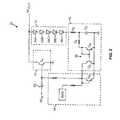
- the present inventionmodifies a power amplifier into a power amplifier circuit 10 , such as illustrated schematically in FIG. 1 .
- the power amplifier circuit 10comprises a power amplifier (PA) 12 , a sensing circuit 14 , a processing circuit 16 , and a bias circuit 18 .
- the power amplifier 12receives an RF IN signal, amplifies it, and produces an RF OUT signal.
- the power amplifier 12also receives a bias signal from the bias circuit 18 .
- the bias circuit 18may be incorporated into the semiconductor having the power amplifier 12 , but need not be.
- the power amplifier 12 , the sensing circuit 14 , the processing circuit 16 , and the bias circuit 18are all printed as a single monolithic integrated circuit, but again, need not be.
- the power amplifier 12may be a transistor cell array comparable to those illustrated in U.S. patent applications Ser. No. 09/878,461, filed Jun. 11, 2001; and Ser. No. 09/952,524, filed Sep. 14, 2001; and U.S. Pat. Nos. 6,265,943; 5,608,353, and 5,629,648, which are all hereby incorporated by reference.
- the power amplifier 12may be a single transistor, and will be represented as such in the subsequent Figures. It is to be understood, however, that despite its representation as a single transistor, the power amplifier 12 may in fact be a transistor array as described in the previously incorporated applications and patents or any other transistor amplifier configuration available to those skilled in the art.
- the sensing circuit 14is coupled to the RF OUT signal and detects whether the RF OUT signal has risen above a predetermined threshold.
- the predetermined thresholdis, in an exemplary embodiment, set below a voltage at which extended operation would cause burnout of the power amplifier 12 .
- the sensing circuit 14outputs a sensed signal to the processing circuit 16 when the predetermined threshold has been exceeded.
- the processing circuit 16receives the sensed signal from the sensing circuit 14 and modifies the bias point provided by the bias circuit 18 so as to reduce the bias provided to the power amplifier 12 . This causes the power amplifier 12 to have a lower output, thus reducing the chance of burnout.
- the precise details of the sensing circuit 14 and the processing circuit 16depend on the embodiment and will be explored further below.
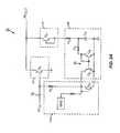
- FIG. 2Aillustrates a circuit level diagram of a first embodiment of the present invention with a first bias circuit 18 A.
- the RF IN signalis coupled to the power amplifier 12 by a capacitor 20 .
- the RF OUT signalis generated by the power amplifier 12 .
- the collector of a transistor Q 1provides the RF OUT signal.
- a transistor Q 3particularly the base-emitter junction of the transistor Q 3 , is used as an avalanche diode to form the sensing circuit 14 .
- the base-emitter junctionbegins to pass current when the applied reverse voltage exceeds a predetermined threshold.
- the predetermined thresholdcomprises approximately 8 V. The current rapidly increases from the microampere range to the milliampere range with a small increase in applied voltage above the conduction threshold.
- a resistor R 3controls the magnitude of the current produced by the transistor Q 3 .
- Resistors R 3 and R 4along with capacitor C 2 , form a low pass filter for filtering the current pulses produced by the transistor Q 3 .
- the filtered currentis then applied to the current mirror 26 comprised of transistors Q 4 and Q 5 .
- the current flowing through Q 4is mirrored across to the transistor Q 5 as a function of the respective sizes of the two transistors.
- the output of the current mirror 26sinks bias current from bias circuit 18 A to ground that was destined for the power amplifier 12 .
- the output of the current mirror 26sinks bias current from bias circuit 18 A to ground that was destined for the power amplifier 12 .
- the output of the current mirror 26sinks bias current from bias circuit 18 A to ground that was destined for the power amplifier 12 .
- the output of the current mirror 26sinks bias current from bias circuit 18 A to ground that was destined for the power amplifier 12 .
- the output of the current mirror 26sinks bias current from bias circuit 18 A to ground that was destined for the power amplifier 12 .
- less currentis presented to diode connected transistor Q 2 .
- resistor R 1for use by the power amplifier 12 . This reduces the bias on the power amplifier 12 when peak RF voltages start approaching the destruction limits of the power amplifier 12 .
- Capacitor C 2sets the loop response time.
- Resistor R 3is determined by the need to limit current spikes through transistor Q 3 .
- the value of R 4determines the rate at which current passes into the current mirror 26 .
- the resistances of resistors R 3 and R 4is 500 ⁇ .
- the capacitor C 2sets the loop time constant.
- the capacitance of capacitor C 2is 1000 pF for loop stability.
- loop time constantit may be preferable to have a relatively long loop time constant. For example, if the loop time constant is short, an inductive pulse may be generated at the RF OUT port from the bias and/or matching network. This passes more current through the transistor Q 3 , causing a regenerative oscillation. A longer loop time constant reduces the rate of change in the collector current of the power amplifier 12 and increases stability.
- a second bias circuit 18 Bis illustrated in FIG. 2 B.
- the bias circuit 18As current increases in the transistor Q 5 , the transistor Q 6 turns off because no current flows in R 2 . As a result, the collector of the transistor Q 2 has little or no current, and the power amplifier 12 has no bias input. Thus, instead of shunting the current to ground, this embodiment significantly reduces or turns off the bias current entirely.
- Bias circuit 18 Bis sometimes referred to as a buffered passive bias network.
- processing circuit 16may be modified as needed to accommodate differing bias circuits 18 .
- the sensing circuit 14may be formed by a string of diodes 28 A- 28 E as illustrated in FIG. 3 .
- the number of diodes 28is determined by the desired threshold voltage above which the feedback loop should be operative. As with the previous embodiment, in this embodiment, this value may be approximately 8 volts.
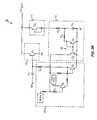
- FIG. 4illustrates yet another alternate embodiment of the sensing circuit 14 .
- the diodes 28 of FIG. 3are replaced with diode connected transistors Q 7 -Q 9 .
- the number of diode connected transistorsis determined by the desired threshold voltage above which the feedback loop should be operative.
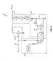
- FIG. 5illustrates still another embodiment of sensing circuit 14 .
- the transistor Q 3 of FIG. 2Ais replaced with a series of transistors that operate as diodes, much like in FIG. 4 .
- a first transistor Q 10cooperates with resistors 54 , 56 to form a base to emitter multiplier circuit as is well understood.
- the resistors 54 , 56act to increase the current that is available when the transistor Q 10 does in fact turn on.
- Transistors Q 11 -Q 13act to increase the threshold voltage of the sensing circuit 14 so normal operation does not actuate the feedback.
Landscapes
- Engineering & Computer Science (AREA)
- Power Engineering (AREA)
- Amplifiers (AREA)
Abstract
Description
Claims (12)
Priority Applications (1)
| Application Number | Priority Date | Filing Date | Title |
|---|---|---|---|
| US10/133,793US6720831B2 (en) | 2002-04-26 | 2002-04-26 | Power amplifier protection circuit |
Applications Claiming Priority (1)
| Application Number | Priority Date | Filing Date | Title |
|---|---|---|---|
| US10/133,793US6720831B2 (en) | 2002-04-26 | 2002-04-26 | Power amplifier protection circuit |
Publications (2)
| Publication Number | Publication Date |
|---|---|
| US20030201835A1 US20030201835A1 (en) | 2003-10-30 |
| US6720831B2true US6720831B2 (en) | 2004-04-13 |
Family
ID=29249054
Family Applications (1)
| Application Number | Title | Priority Date | Filing Date |
|---|---|---|---|
| US10/133,793Expired - LifetimeUS6720831B2 (en) | 2002-04-26 | 2002-04-26 | Power amplifier protection circuit |
Country Status (1)
| Country | Link |
|---|---|
| US (1) | US6720831B2 (en) |
Cited By (48)
| Publication number | Priority date | Publication date | Assignee | Title |
|---|---|---|---|---|
| US20030215026A1 (en)* | 2002-05-16 | 2003-11-20 | Hietala Alexander Wayne | AM to AM correction system for polar modulator |
| US20030215025A1 (en)* | 2002-05-16 | 2003-11-20 | Hietala Alexander Wayne | AM to PM correction system for polar modulator |
| US6831506B1 (en) | 2003-09-17 | 2004-12-14 | Rf Micro Devices, Inc. | Reconfigurable filter architecture |
| US20050030106A1 (en)* | 2003-08-08 | 2005-02-10 | Mitsubishi Denki Kabushiki Kaisha | Output overvoltage protection circuit for power amplifier |
| US20050088237A1 (en)* | 2003-10-22 | 2005-04-28 | Rf Micro Devices, Inc. | Temperature compensated power amplifier power control |
| US6906584B1 (en) | 2003-12-10 | 2005-06-14 | Rf Micro Devices, Inc. | Switchable gain amplifier having a high-pass filter pole |
| US20050253655A1 (en)* | 2004-05-12 | 2005-11-17 | Gregory Yuen | Amplifier bias enhancement technique |
| US6970040B1 (en) | 2003-11-13 | 2005-11-29 | Rf Micro Devices, Inc. | Multi-mode/multi-band power amplifier |
| US7026665B1 (en) | 2003-09-19 | 2006-04-11 | Rf Micro Devices, Inc. | High voltage GaN-based transistor structure |
| US20060087377A1 (en)* | 2002-10-30 | 2006-04-27 | Koninklijke Philips Electronics N.V. | Amplifier bias circuit, method for biasing an amplifier and integrated circuit comprising an amplifier bias circuit |
| US20060214734A1 (en)* | 2005-03-23 | 2006-09-28 | Lg Electronics Inc. | Power protecting apparatus and method for power amplifier |
| US20060267688A1 (en)* | 2005-05-11 | 2006-11-30 | Renesas Technology Corp. | High frequency power amplifier, transmitter and mobile communication terminal using the power amplifier |
| US7218175B1 (en)* | 2005-04-11 | 2007-05-15 | Sirenza Microdevices, Inc. | Dynamic feedback linearization |
| US7256650B1 (en) | 2005-02-28 | 2007-08-14 | Rf Micro Devices, Inc. | VSWR tolerant power detector |
| US7268990B1 (en)* | 2003-05-15 | 2007-09-11 | Marvell International Ltd. | Power amplifier protection |
| US20080174356A1 (en)* | 2006-12-13 | 2008-07-24 | Mitsubishi Electric Corporation | Wave detector circuit |
| US20080186092A1 (en)* | 2006-10-26 | 2008-08-07 | Infineon Technologies Ag | Shared linearity maintenance in power amplifiers |
| US7440734B1 (en) | 2006-02-06 | 2008-10-21 | Rf Micro Devices, Inc. | Active quadrature radio frequency power detector |
| US7529523B1 (en) | 2004-08-23 | 2009-05-05 | Rf Micro Devices, Inc. | N-th order curve fit for power calibration in a mobile terminal |
| US7545880B1 (en) | 2004-06-23 | 2009-06-09 | Rf Micro Devices, Inc. | Multiple polynomial digital predistortion |
| US20090309663A1 (en)* | 2008-06-13 | 2009-12-17 | Freescale Semiconductor, Inc. | Power amplifiers having improved protection against avalanche current |
| US7689182B1 (en) | 2006-10-12 | 2010-03-30 | Rf Micro Devices, Inc. | Temperature compensated bias for AM/PM improvement |
| US7863984B1 (en)* | 2009-07-17 | 2011-01-04 | Vivant Medical, Inc. | High efficiency microwave amplifier |
| US7877060B1 (en) | 2006-02-06 | 2011-01-25 | Rf Micro Devices, Inc. | Fast calibration of AM/PM pre-distortion |
| US7962108B1 (en) | 2006-03-29 | 2011-06-14 | Rf Micro Devices, Inc. | Adaptive AM/PM compensation |
| US8009762B1 (en) | 2007-04-17 | 2011-08-30 | Rf Micro Devices, Inc. | Method for calibrating a phase distortion compensated polar modulated radio frequency transmitter |
| US8224265B1 (en) | 2005-06-13 | 2012-07-17 | Rf Micro Devices, Inc. | Method for optimizing AM/AM and AM/PM predistortion in a mobile terminal |
| US8258876B1 (en) | 2011-01-07 | 2012-09-04 | Anadigics, Inc. | Power amplifier protection circuit |
| US8489042B1 (en) | 2009-10-08 | 2013-07-16 | Rf Micro Devices, Inc. | Polar feedback linearization |
| US20140035683A1 (en)* | 2011-10-28 | 2014-02-06 | Kabushiki Kaisha Toshiba | Integrated circuit |
| US8988097B2 (en) | 2012-08-24 | 2015-03-24 | Rf Micro Devices, Inc. | Method for on-wafer high voltage testing of semiconductor devices |
| US9070761B2 (en) | 2012-08-27 | 2015-06-30 | Rf Micro Devices, Inc. | Field effect transistor (FET) having fingers with rippled edges |
| US9093420B2 (en) | 2012-04-18 | 2015-07-28 | Rf Micro Devices, Inc. | Methods for fabricating high voltage field effect transistor finger terminations |
| US9124221B2 (en) | 2012-07-16 | 2015-09-01 | Rf Micro Devices, Inc. | Wide bandwidth radio frequency amplier having dual gate transistors |
| US9129802B2 (en) | 2012-08-27 | 2015-09-08 | Rf Micro Devices, Inc. | Lateral semiconductor device with vertical breakdown region |
| US9142620B2 (en) | 2012-08-24 | 2015-09-22 | Rf Micro Devices, Inc. | Power device packaging having backmetals couple the plurality of bond pads to the die backside |
| US9147632B2 (en) | 2012-08-24 | 2015-09-29 | Rf Micro Devices, Inc. | Semiconductor device having improved heat dissipation |
| US9202874B2 (en) | 2012-08-24 | 2015-12-01 | Rf Micro Devices, Inc. | Gallium nitride (GaN) device with leakage current-based over-voltage protection |
| US20160099688A1 (en)* | 2014-10-03 | 2016-04-07 | Skyworks Solutions, Inc. | Peak voltage limiting circuits and methods for power amplifiers |
| US9325281B2 (en) | 2012-10-30 | 2016-04-26 | Rf Micro Devices, Inc. | Power amplifier controller |
| US9455327B2 (en) | 2014-06-06 | 2016-09-27 | Qorvo Us, Inc. | Schottky gated transistor with interfacial layer |
| US9536803B2 (en) | 2014-09-05 | 2017-01-03 | Qorvo Us, Inc. | Integrated power module with improved isolation and thermal conductivity |
| US9917080B2 (en) | 2012-08-24 | 2018-03-13 | Qorvo US. Inc. | Semiconductor device with electrical overstress (EOS) protection |
| US10062684B2 (en) | 2015-02-04 | 2018-08-28 | Qorvo Us, Inc. | Transition frequency multiplier semiconductor device |
| US10425046B1 (en) | 2018-03-29 | 2019-09-24 | Qorvo Us Inc. | Differential power amplifier |
| CN110808719A (en)* | 2018-08-06 | 2020-02-18 | 亚德诺半导体无限责任公司 | Breakdown protection circuit for power amplifier |
| US10615158B2 (en) | 2015-02-04 | 2020-04-07 | Qorvo Us, Inc. | Transition frequency multiplier semiconductor device |
| US11303252B2 (en) | 2019-09-25 | 2022-04-12 | Analog Devices International Unlimited Company | Breakdown protection circuit for power amplifier |
Families Citing this family (17)
| Publication number | Priority date | Publication date | Assignee | Title |
|---|---|---|---|---|
| US7355470B2 (en) | 2006-04-24 | 2008-04-08 | Parkervision, Inc. | Systems and methods of RF power transmission, modulation, and amplification, including embodiments for amplifier class transitioning |
| US7327803B2 (en) | 2004-10-22 | 2008-02-05 | Parkervision, Inc. | Systems and methods for vector power amplification |
| US9106316B2 (en) | 2005-10-24 | 2015-08-11 | Parkervision, Inc. | Systems and methods of RF power transmission, modulation, and amplification |
| US7911272B2 (en) | 2007-06-19 | 2011-03-22 | Parkervision, Inc. | Systems and methods of RF power transmission, modulation, and amplification, including blended control embodiments |
| US20130078934A1 (en) | 2011-04-08 | 2013-03-28 | Gregory Rawlins | Systems and Methods of RF Power Transmission, Modulation, and Amplification |
| US8334722B2 (en) | 2007-06-28 | 2012-12-18 | Parkervision, Inc. | Systems and methods of RF power transmission, modulation and amplification |
| EP1811658A1 (en)* | 2006-01-24 | 2007-07-25 | Alcatel Lucent | Power amplifier bias protection for depletion mode transistor |
| US7937106B2 (en) | 2006-04-24 | 2011-05-03 | ParkerVision, Inc, | Systems and methods of RF power transmission, modulation, and amplification, including architectural embodiments of same |
| US8031804B2 (en) | 2006-04-24 | 2011-10-04 | Parkervision, Inc. | Systems and methods of RF tower transmission, modulation, and amplification, including embodiments for compensating for waveform distortion |
| WO2008144017A1 (en) | 2007-05-18 | 2008-11-27 | Parkervision, Inc. | Systems and methods of rf power transmission, modulation, and amplification |
| WO2008156800A1 (en) | 2007-06-19 | 2008-12-24 | Parkervision, Inc. | Combiner-less multiple input single output (miso) amplification with blended control |
| KR20140034895A (en) | 2011-06-02 | 2014-03-20 | 파커비전, 인크. | Antenna control |
| EP2634917B1 (en)* | 2012-02-28 | 2015-04-08 | ST-Ericsson SA | Protection module for RF-amplifier |
| CN106415435B (en) | 2013-09-17 | 2020-08-11 | 帕克维辛股份有限公司 | Method, apparatus, and system for presenting information-carrying time functions |
| CN110731048B (en)* | 2017-12-04 | 2023-03-24 | 阿塞尔桑电子工业及贸易股份公司 | Active confinement system |
| TWI699964B (en)* | 2018-06-15 | 2020-07-21 | 立積電子股份有限公司 | Bias circuit |
| TWI710210B (en) | 2019-06-13 | 2020-11-11 | 立積電子股份有限公司 | Bias device |
Citations (5)
| Publication number | Priority date | Publication date | Assignee | Title |
|---|---|---|---|---|
| US5083096A (en)* | 1989-05-31 | 1992-01-21 | Nec Corporation | High frequency amplifier circuit capable of optimizing a total power consumption |
| US5543760A (en)* | 1993-03-05 | 1996-08-06 | Pioneer Electronic Corporation | Protection circuit for a power amplifier |
| US5903192A (en)* | 1996-02-23 | 1999-05-11 | Daimler-Benz Aerospace Ag | Arrangement for controlling the output amplitude of a high frequency power amplifier |
| US6459340B1 (en)* | 2001-05-31 | 2002-10-01 | Triquint Semiconductor, Inc. | Power amplifier mismatch protection with clamping diodes in RF feedback circuit |
| US6525611B1 (en)* | 2001-08-01 | 2003-02-25 | Rf Micro Devices, Inc. | Power amplifier protection |
- 2002
- 2002-04-26USUS10/133,793patent/US6720831B2/ennot_activeExpired - Lifetime
Patent Citations (5)
| Publication number | Priority date | Publication date | Assignee | Title |
|---|---|---|---|---|
| US5083096A (en)* | 1989-05-31 | 1992-01-21 | Nec Corporation | High frequency amplifier circuit capable of optimizing a total power consumption |
| US5543760A (en)* | 1993-03-05 | 1996-08-06 | Pioneer Electronic Corporation | Protection circuit for a power amplifier |
| US5903192A (en)* | 1996-02-23 | 1999-05-11 | Daimler-Benz Aerospace Ag | Arrangement for controlling the output amplitude of a high frequency power amplifier |
| US6459340B1 (en)* | 2001-05-31 | 2002-10-01 | Triquint Semiconductor, Inc. | Power amplifier mismatch protection with clamping diodes in RF feedback circuit |
| US6525611B1 (en)* | 2001-08-01 | 2003-02-25 | Rf Micro Devices, Inc. | Power amplifier protection |
Non-Patent Citations (1)
| Title |
|---|
| Pusl, Joe et al., "SiGe Power Amplifier ICs with SWR Protection for Handset Applications," Microwave Journal 44, No. 6, Jun. 2001. |
Cited By (75)
| Publication number | Priority date | Publication date | Assignee | Title |
|---|---|---|---|---|
| US20030215026A1 (en)* | 2002-05-16 | 2003-11-20 | Hietala Alexander Wayne | AM to AM correction system for polar modulator |
| US20030215025A1 (en)* | 2002-05-16 | 2003-11-20 | Hietala Alexander Wayne | AM to PM correction system for polar modulator |
| US7801244B2 (en) | 2002-05-16 | 2010-09-21 | Rf Micro Devices, Inc. | Am to AM correction system for polar modulator |
| US7991071B2 (en) | 2002-05-16 | 2011-08-02 | Rf Micro Devices, Inc. | AM to PM correction system for polar modulator |
| US7286016B2 (en)* | 2002-10-30 | 2007-10-23 | Nxp B.V. | Amplifier bias circuit, method for biasing an amplifier and integrated circuit comprising an amplifier bias circuit |
| US20060087377A1 (en)* | 2002-10-30 | 2006-04-27 | Koninklijke Philips Electronics N.V. | Amplifier bias circuit, method for biasing an amplifier and integrated circuit comprising an amplifier bias circuit |
| US7606016B1 (en) | 2003-05-15 | 2009-10-20 | Marvell International Ltd. | Power amplifier protection |
| US7864498B1 (en) | 2003-05-15 | 2011-01-04 | Marvell International Ltd. | Power amplifier protection |
| US8179648B1 (en) | 2003-05-15 | 2012-05-15 | Marvell International Ltd. | Power amplifier protection |
| US7268990B1 (en)* | 2003-05-15 | 2007-09-11 | Marvell International Ltd. | Power amplifier protection |
| US7145397B2 (en)* | 2003-08-08 | 2006-12-05 | Mitsubishi Denki Kabushiki Kaisha | Output overvoltage protection circuit for power amplifier |
| US20050030106A1 (en)* | 2003-08-08 | 2005-02-10 | Mitsubishi Denki Kabushiki Kaisha | Output overvoltage protection circuit for power amplifier |
| US6831506B1 (en) | 2003-09-17 | 2004-12-14 | Rf Micro Devices, Inc. | Reconfigurable filter architecture |
| US7459356B1 (en) | 2003-09-19 | 2008-12-02 | Rf Micro Devices, Inc. | High voltage GaN-based transistor structure |
| US7026665B1 (en) | 2003-09-19 | 2006-04-11 | Rf Micro Devices, Inc. | High voltage GaN-based transistor structure |
| US7968391B1 (en) | 2003-09-19 | 2011-06-28 | Rf Micro Devices, Inc. | High voltage GaN-based transistor structure |
| US20050088237A1 (en)* | 2003-10-22 | 2005-04-28 | Rf Micro Devices, Inc. | Temperature compensated power amplifier power control |
| US6998919B2 (en) | 2003-10-22 | 2006-02-14 | Rf Micro Devices, Inc. | Temperature compensated power amplifier power control |
| US6970040B1 (en) | 2003-11-13 | 2005-11-29 | Rf Micro Devices, Inc. | Multi-mode/multi-band power amplifier |
| US6906584B1 (en) | 2003-12-10 | 2005-06-14 | Rf Micro Devices, Inc. | Switchable gain amplifier having a high-pass filter pole |
| US20050253655A1 (en)* | 2004-05-12 | 2005-11-17 | Gregory Yuen | Amplifier bias enhancement technique |
| US7049891B2 (en)* | 2004-05-12 | 2006-05-23 | Sige Semiconductor Inc. | Amplifier bias enhancement technique |
| US7545880B1 (en) | 2004-06-23 | 2009-06-09 | Rf Micro Devices, Inc. | Multiple polynomial digital predistortion |
| US7551686B1 (en) | 2004-06-23 | 2009-06-23 | Rf Micro Devices, Inc. | Multiple polynomial digital predistortion |
| US7529523B1 (en) | 2004-08-23 | 2009-05-05 | Rf Micro Devices, Inc. | N-th order curve fit for power calibration in a mobile terminal |
| US7256650B1 (en) | 2005-02-28 | 2007-08-14 | Rf Micro Devices, Inc. | VSWR tolerant power detector |
| US7482877B2 (en)* | 2005-03-23 | 2009-01-27 | Lg Electronics Inc. | Power protecting apparatus and method for power amplifier |
| US20060214734A1 (en)* | 2005-03-23 | 2006-09-28 | Lg Electronics Inc. | Power protecting apparatus and method for power amplifier |
| US7218175B1 (en)* | 2005-04-11 | 2007-05-15 | Sirenza Microdevices, Inc. | Dynamic feedback linearization |
| US8306490B2 (en) | 2005-05-11 | 2012-11-06 | Renesas Electronics Corporation | High frequency power amplifier, transmitter and mobile communication terminal using the power amplifier |
| US8229373B2 (en) | 2005-05-11 | 2012-07-24 | Renesas Electronics Corporation | High frequency power amplifier, transmitter and mobile communication terminal using the power amplifier |
| US20060267688A1 (en)* | 2005-05-11 | 2006-11-30 | Renesas Technology Corp. | High frequency power amplifier, transmitter and mobile communication terminal using the power amplifier |
| US8224265B1 (en) | 2005-06-13 | 2012-07-17 | Rf Micro Devices, Inc. | Method for optimizing AM/AM and AM/PM predistortion in a mobile terminal |
| US7877060B1 (en) | 2006-02-06 | 2011-01-25 | Rf Micro Devices, Inc. | Fast calibration of AM/PM pre-distortion |
| US7440734B1 (en) | 2006-02-06 | 2008-10-21 | Rf Micro Devices, Inc. | Active quadrature radio frequency power detector |
| US7962108B1 (en) | 2006-03-29 | 2011-06-14 | Rf Micro Devices, Inc. | Adaptive AM/PM compensation |
| US7689182B1 (en) | 2006-10-12 | 2010-03-30 | Rf Micro Devices, Inc. | Temperature compensated bias for AM/PM improvement |
| US20080186092A1 (en)* | 2006-10-26 | 2008-08-07 | Infineon Technologies Ag | Shared linearity maintenance in power amplifiers |
| US7557653B2 (en)* | 2006-10-26 | 2009-07-07 | Infineon Technologies Ag | Shared linearity maintenance in power amplifiers |
| US20080174356A1 (en)* | 2006-12-13 | 2008-07-24 | Mitsubishi Electric Corporation | Wave detector circuit |
| US7705658B2 (en)* | 2006-12-13 | 2010-04-27 | Mitsubishi Electric Corporation | Wave detector circuit |
| US8009762B1 (en) | 2007-04-17 | 2011-08-30 | Rf Micro Devices, Inc. | Method for calibrating a phase distortion compensated polar modulated radio frequency transmitter |
| US20090309663A1 (en)* | 2008-06-13 | 2009-12-17 | Freescale Semiconductor, Inc. | Power amplifiers having improved protection against avalanche current |
| US7795980B2 (en) | 2008-06-13 | 2010-09-14 | Freescale Semiconductor, Inc. | Power amplifiers having improved protection against avalanche current |
| US7863984B1 (en)* | 2009-07-17 | 2011-01-04 | Vivant Medical, Inc. | High efficiency microwave amplifier |
| US20110012679A1 (en)* | 2009-07-17 | 2011-01-20 | Tyco Healthcare Group Lp | High efficiency microwave amplifier |
| AU2010203036B2 (en)* | 2009-07-17 | 2013-10-31 | Covidien Lp | High efficiency microwave amplifier |
| US8489042B1 (en) | 2009-10-08 | 2013-07-16 | Rf Micro Devices, Inc. | Polar feedback linearization |
| US8258876B1 (en) | 2011-01-07 | 2012-09-04 | Anadigics, Inc. | Power amplifier protection circuit |
| US20140035683A1 (en)* | 2011-10-28 | 2014-02-06 | Kabushiki Kaisha Toshiba | Integrated circuit |
| US9214910B2 (en)* | 2011-10-28 | 2015-12-15 | Kabushiki Kaisha Toshiba | Integrated circuit |
| US9093420B2 (en) | 2012-04-18 | 2015-07-28 | Rf Micro Devices, Inc. | Methods for fabricating high voltage field effect transistor finger terminations |
| US9564497B2 (en) | 2012-04-18 | 2017-02-07 | Qorvo Us, Inc. | High voltage field effect transitor finger terminations |
| US9136341B2 (en) | 2012-04-18 | 2015-09-15 | Rf Micro Devices, Inc. | High voltage field effect transistor finger terminations |
| US9124221B2 (en) | 2012-07-16 | 2015-09-01 | Rf Micro Devices, Inc. | Wide bandwidth radio frequency amplier having dual gate transistors |
| US9142620B2 (en) | 2012-08-24 | 2015-09-22 | Rf Micro Devices, Inc. | Power device packaging having backmetals couple the plurality of bond pads to the die backside |
| US9147632B2 (en) | 2012-08-24 | 2015-09-29 | Rf Micro Devices, Inc. | Semiconductor device having improved heat dissipation |
| US9202874B2 (en) | 2012-08-24 | 2015-12-01 | Rf Micro Devices, Inc. | Gallium nitride (GaN) device with leakage current-based over-voltage protection |
| US8988097B2 (en) | 2012-08-24 | 2015-03-24 | Rf Micro Devices, Inc. | Method for on-wafer high voltage testing of semiconductor devices |
| US9917080B2 (en) | 2012-08-24 | 2018-03-13 | Qorvo US. Inc. | Semiconductor device with electrical overstress (EOS) protection |
| US9640632B2 (en) | 2012-08-24 | 2017-05-02 | Qorvo Us, Inc. | Semiconductor device having improved heat dissipation |
| US9129802B2 (en) | 2012-08-27 | 2015-09-08 | Rf Micro Devices, Inc. | Lateral semiconductor device with vertical breakdown region |
| US9070761B2 (en) | 2012-08-27 | 2015-06-30 | Rf Micro Devices, Inc. | Field effect transistor (FET) having fingers with rippled edges |
| US9325281B2 (en) | 2012-10-30 | 2016-04-26 | Rf Micro Devices, Inc. | Power amplifier controller |
| US9455327B2 (en) | 2014-06-06 | 2016-09-27 | Qorvo Us, Inc. | Schottky gated transistor with interfacial layer |
| US9536803B2 (en) | 2014-09-05 | 2017-01-03 | Qorvo Us, Inc. | Integrated power module with improved isolation and thermal conductivity |
| US20160099688A1 (en)* | 2014-10-03 | 2016-04-07 | Skyworks Solutions, Inc. | Peak voltage limiting circuits and methods for power amplifiers |
| US10284153B2 (en)* | 2014-10-03 | 2019-05-07 | Skyworks Solutions, Inc. | Peak voltage limiting circuits and methods for power amplifiers |
| US10062684B2 (en) | 2015-02-04 | 2018-08-28 | Qorvo Us, Inc. | Transition frequency multiplier semiconductor device |
| US10615158B2 (en) | 2015-02-04 | 2020-04-07 | Qorvo Us, Inc. | Transition frequency multiplier semiconductor device |
| US10425046B1 (en) | 2018-03-29 | 2019-09-24 | Qorvo Us Inc. | Differential power amplifier |
| CN110808719A (en)* | 2018-08-06 | 2020-02-18 | 亚德诺半导体无限责任公司 | Breakdown protection circuit for power amplifier |
| US10797656B2 (en)* | 2018-08-06 | 2020-10-06 | Analong Devices Global Unlimited Company | Breakdown protection circuit for power amplifier |
| CN110808719B (en)* | 2018-08-06 | 2024-05-17 | 亚德诺半导体国际无限责任公司 | Breakdown protection circuit for power amplifier |
| US11303252B2 (en) | 2019-09-25 | 2022-04-12 | Analog Devices International Unlimited Company | Breakdown protection circuit for power amplifier |
Also Published As
| Publication number | Publication date |
|---|---|
| US20030201835A1 (en) | 2003-10-30 |
Similar Documents
| Publication | Publication Date | Title |
|---|---|---|
| US6720831B2 (en) | Power amplifier protection circuit | |
| US6525611B1 (en) | Power amplifier protection | |
| US7348847B2 (en) | Integrated implementation of a collector boost scheme and method therefor | |
| KR100853259B1 (en) | High frequency power amplifier circuit | |
| US7106137B2 (en) | Method and apparatus for controlling the output power of a power amplifier | |
| US7898299B2 (en) | Current sense amplifier | |
| US3959713A (en) | Solid state current limit circuit | |
| US6137366A (en) | High VSWR mismatch output stage | |
| US20100155627A1 (en) | Methods and apparatuses for performing common mode pulse compensation in an opto-isolator | |
| US7692491B2 (en) | Radio-frequency power amplifier | |
| KR102066008B1 (en) | Low noise amplifier with improved absolute maximum rating performance | |
| KR20230003517A (en) | Amplifier with Input Power Protection | |
| US4451801A (en) | Wideband linear carrier current amplifier | |
| US7057462B2 (en) | Temperature compensated on-chip bias circuit for linear RF HBT power amplifiers | |
| WO1995017042A1 (en) | An amplifier for use in a radiotelephone | |
| KR102778143B1 (en) | Power amplifier and power amplifier module | |
| US6909585B2 (en) | Protection circuit protecting against voltage irregularities | |
| US6002922A (en) | Method and apparatus for detecting communication signals | |
| US10187019B1 (en) | Phased array antenna system | |
| US5517684A (en) | Radio communication system having current control circuit | |
| EP0789452B1 (en) | A power amplifier with bootstrap voltage clamp | |
| US20070297106A1 (en) | Esd and electric surge protected circuit and method of making same | |
| US6882512B2 (en) | Integrated circuit provided with a protection against electrostatic discharges | |
| EP0408137B1 (en) | Amplifier arrangement | |
| JPH07147726A (en) | Overvoltage limiting circuit for semiconductor device |
Legal Events
| Date | Code | Title | Description |
|---|---|---|---|
| AS | Assignment | Owner name:RF MICRO DEVICES, INC., NORTH CAROLINA Free format text:ASSIGNMENT OF ASSIGNORS INTEREST;ASSIGNORS:DENING, DAVID;MUHONEN, KATHLEEN;REEL/FRAME:012847/0894 Effective date:20020424 | |
| STCF | Information on status: patent grant | Free format text:PATENTED CASE | |
| FPAY | Fee payment | Year of fee payment:4 | |
| FPAY | Fee payment | Year of fee payment:8 | |
| AS | Assignment | Owner name:BANK OF AMERICA, N.A., AS ADMINISTRATIVE AGENT, TE Free format text:NOTICE OF GRANT OF SECURITY INTEREST IN PATENTS;ASSIGNOR:RF MICRO DEVICES, INC.;REEL/FRAME:030045/0831 Effective date:20130319 | |
| AS | Assignment | Owner name:RF MICRO DEVICES, INC., NORTH CAROLINA Free format text:TERMINATION AND RELEASE OF SECURITY INTEREST IN PATENTS (RECORDED 3/19/13 AT REEL/FRAME 030045/0831);ASSIGNOR:BANK OF AMERICA, N.A., AS ADMINISTRATIVE AGENT;REEL/FRAME:035334/0363 Effective date:20150326 | |
| FPAY | Fee payment | Year of fee payment:12 | |
| AS | Assignment | Owner name:QORVO US, INC., NORTH CAROLINA Free format text:MERGER;ASSIGNOR:RF MICRO DEVICES, INC.;REEL/FRAME:039196/0941 Effective date:20160330 |