US6720261B1 - Method and system for eliminating extrusions in semiconductor vias - Google Patents
Method and system for eliminating extrusions in semiconductor viasDownload PDFInfo
- Publication number
- US6720261B1 US6720261B1US09/586,586US58658600AUS6720261B1US 6720261 B1US6720261 B1US 6720261B1US 58658600 AUS58658600 AUS 58658600AUS 6720261 B1US6720261 B1US 6720261B1
- Authority
- US
- United States
- Prior art keywords
- interconnect
- layers
- temperature
- extrusions
- coating
- Prior art date
- Legal status (The legal status is an assumption and is not a legal conclusion. Google has not performed a legal analysis and makes no representation as to the accuracy of the status listed.)
- Expired - Lifetime
Links
Images


Classifications
- H—ELECTRICITY
- H01—ELECTRIC ELEMENTS
- H01L—SEMICONDUCTOR DEVICES NOT COVERED BY CLASS H10
- H01L21/00—Processes or apparatus adapted for the manufacture or treatment of semiconductor or solid state devices or of parts thereof
- H01L21/70—Manufacture or treatment of devices consisting of a plurality of solid state components formed in or on a common substrate or of parts thereof; Manufacture of integrated circuit devices or of parts thereof
- H01L21/71—Manufacture of specific parts of devices defined in group H01L21/70
- H01L21/768—Applying interconnections to be used for carrying current between separate components within a device comprising conductors and dielectrics
- H01L21/76838—Applying interconnections to be used for carrying current between separate components within a device comprising conductors and dielectrics characterised by the formation and the after-treatment of the conductors
- H01L21/76841—Barrier, adhesion or liner layers
- H01L21/76843—Barrier, adhesion or liner layers formed in openings in a dielectric
- Y—GENERAL TAGGING OF NEW TECHNOLOGICAL DEVELOPMENTS; GENERAL TAGGING OF CROSS-SECTIONAL TECHNOLOGIES SPANNING OVER SEVERAL SECTIONS OF THE IPC; TECHNICAL SUBJECTS COVERED BY FORMER USPC CROSS-REFERENCE ART COLLECTIONS [XRACs] AND DIGESTS
- Y02—TECHNOLOGIES OR APPLICATIONS FOR MITIGATION OR ADAPTATION AGAINST CLIMATE CHANGE
- Y02P—CLIMATE CHANGE MITIGATION TECHNOLOGIES IN THE PRODUCTION OR PROCESSING OF GOODS
- Y02P80/00—Climate change mitigation technologies for sector-wide applications
- Y02P80/30—Reducing waste in manufacturing processes; Calculations of released waste quantities
Definitions
- the invention disclosed hereinrelates generally to a method and apparatus for fabricating semiconductor integrated circuit devices. More particularly, the present invention relates to method and apparatus for eliminating interconnect extrusions in vias.
- Multilevel metallizationis used to conserve chip area while minimizing interconnection resistance.
- Aluminum and aluminum alloysare generally the predominant interconnect material in metallization systems, but aluminum from the underlying interconnect metallization extrudes into vias during conventional ionized metal plasma (“IMP”) processing of the adhesion and barrier layers used for the formation of tungsten plugs in vias.
- IMPionized metal plasma
- interconnectsare formed over metal contacts to provide electrically conductive paths.
- a dielectric layeris deposited by conventional processes on the metal interconnects. This dielectric layer is etched to form a window or via to expose a portion of the interconnect where the electrical interconnection will be made.
- the viais then filled with electrically conductive material.
- adhesion and barrier layersare used to line the inside of the via before filling the via with an electrically conductive plug material, such as tungsten, copper or copper alloys. Vias are used to electrically connect the metal interconnects on subsequent interconnect levels.
- CMOScomplimentary metal oxide semiconductor
- a plurality of contacts 124 over the doped source and drain regions 118may be formed by conventional processes. These contacts 124 are typically made from interconnect materials, such as aluminum, aluminum alloys, tungsten, or other suitable electrically conducting materials known to one skilled in the art.
- a plurality of interconnects 140are patterned by photolithography and formed using plasma processing over the metal contacts 124 to form electrically conductive paths. For example, the contact windows 124 may be filled with tungsten deposited using techniques well known in the prior art. The structures may then be planarized using chemical-mechanical polishing or etch-back techniques to form tungsten plugs. A layer of conductive metals is then depositied to form the runners or interconnects 140 .
- the interconnectsare made of electrically conductive materials, such as aluminum, aluminum-copper alloys, aluminum-silicon-copper alloys and other aluminum alloys known to one skilled in the art. These aluminum-alloys may be deposited with refractory material under-layers such as titanium, titanium nitride or combinations of both. These multilevel metal stacks may be deposited using sputter deposition techniques, patterned and etched using methods well known in the prior art. A second dielectric layer 142 is deposited by conventional processes on the runners or interconnects 140 . Substrates 100 typically may include several interconnect layers 150 , wherein a plurality of vias 144 are used to electrically connect the metal interconnects or runners 140 on subsequent interconnect levels.
- FIG. 2a schematic sectional view of a conventional via structure is illustrated.
- the via 144is lined with a coating 155 by IMP techniques.
- the coatingwill comprise two layers, an adhesion layer 160 which is coated with a barrier layer 165 .
- the composition of the adhesion layer 160 /barrier layer 165is generally Ti/TiN, Ta/TaN, W/WN or other materials known to one skilled in the art.
- a plug 170is then formed over the barrier layer 165 to fill in the via 144 .
- the plug 170is comprised of tungsten or other materials known to one skilled in the art.
- the plugis deposited using conventional methods known to one skilled in the art, such as chemical vapor deposition (“CVD”) techniques.
- CVDchemical vapor deposition
- interconnects 166For devices that have large current requirements, designers often route the signals through higher metal interconnect levels, such as the final two levels of metal interconnects 168 shown in FIG. 3 . To capitalize on the lower resistivity of copper compared to aluminum, designers often use copper and copper alloys and other materials known to those skilled in the art as the interconnect materials for these high level interconnects 166 .
- the interconnects 166are surrounded by dielectric layers 162 , 163 , and 164 .
- the vias 167connect the interconnects 166 to form electrically conductive paths.
- the most common methods used today for depositing copper and copper alloysis electroplating.
- To deposit copper and copper alloys using an electroplating techniquerequires the deposition of a conductive seeding layer prior to deposition of the copper or copper alloy plug.
- FIG. 4a schematic sectional view of a conventional via structure for higher level metal interconnects 168 is illustrated.
- the via 167is lined with a coating 177 .
- the deposition of copperalso requires the prior deposition of an adhesion and barrier layer stack where copper is used in the damascene or dual damascene structures fabricated in the dielectric.
- the coatingwill comprise three layers, an adhesion layer 172 which is coated with a barrier layer 174 which is then coated with a sceding layer 176 .
- the coating 177may consist of only one, or may consist of more than two layers. Since copper migrates very rapidly through dielectrics, it is contained by depositing barrier layer(s) 174 prior to deposition of the seeding layer 176 . Those skilled in the art will recognize that a preferred method of depositing the adhesion layer 172 and barrier layer 174 stack is IMP. One skilled in the art will recognize that the adhesion and barrier layer(s) may be comprised of one or more layers of tantalum/tantalum nitride/tantalum silicon nitride, tungsten/tungsten nitride/tungsten silicon nitride, titanium/titanium nitride or combinations thereof. Copper and copper alloys are the preferred choice for the seeding layer 176 . Those skilled in the art will also recognize that a preferred method of depositing the seeding layer 176 is IMP.
- the wafertends to be heated due to highly localized heating effects. This heat is derived from the plasma, the RF coil used to generate the plasma, and the latent heat of condensation from ion bombardment from the materials being deposited on the wafer. The temperature during IMP processing gets hot enough to result in the aluminum from the underlying interconnect metallization extruding into the vias.
- the extrusion of the aluminum from the underlying metallization layeralso occurs during IMP deposition of the adhesion/barrier/seeding layers in devices where the higher interconnect levels are copper and the lower level interconnects are aluminum.
- the higher interconnect levelsare copper and the lower level interconnects are aluminum.
- the aluminum from the fourth interconnect levelextrudes through the via from the fourth level to the fifth interconnect level.
- the above and other objectsare achieved by controlling the interconnect temperature during IMP processing.
- the extrusions of interconnect metallizationoccur while wafers are subject to elevated temperatures that cause the internal stresses in the interconnect Metallization to transit from a substantially tensile mode to a substantially compressive mode. Once the interconnect metallization is under compression, it relieves stress by extruding into the via etched into the inter-level dielectric on top of the interconnect metallization.
- interconnect extrusions in viasare eliminated. By eliminating these extrusions, wafer reliability is improved and processing yield loss due to a high number of defects is decreased.
- the interconnect temperatureis controlled by using an actively cooled pedestal in combination with a low temperature IMP deposition process, thereby preventing aluminum extrusions from poisoning the vias.
- the IMP processing timeis decreased to limit heating of the interconnect.
- FIG. 1is a schematic sectional view of the first two layers of a prior art submicron, twin-tub, complimentary metal oxide semiconductor (CMOS) device showing one of a plurality of interconnect levels;
- CMOScomplimentary metal oxide semiconductor
- FIG. 2is a schematic sectional view of a prior art via metallization structure of the first two layers of a semiconductor device
- FIG. 3is a schematic sectional view of the higher level interconnect layers of a semiconductor device
- FIG. 4is a schematic sectional view of a prior art via metallization structure of the high level interconnects in a semiconductor device
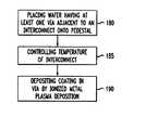
- FIG. 5is a flow diagram of one embodiment of the present invention of a method for eliminating interconnect extrusions in vias
- FIG. 6is a schematic sectional view of one embodiment of the present invention for a system for eliminating interconnect extrusions in vias;
- FIG. 7is a scanning electron micrograph showing interconnect extrusions into the vias from the conventional process
- FIG. 8is a scanning electron micrograph showing no extrusions into the vias from the process of one embodiment of the present invention.
- FIG. 5depicts an example embodiment of the process of the present invention.
- at least one wafer having at least one via 144 adjacent to an interconnect 140is placed onto a pedestal 205 in step 180 .
- the interconnect 140is typically made from aluminum, aluminum alloys and other materials known to one skilled in the art.
- the interconnect metallizationis deposited onto the wafer by processing techniques known to those skilled in the art, such as plasma vapor deposition, the interconnect metallization is generally in a substantially tensile mode.
- step 185the temperature of the interconnect 140 is controlled.
- the temperatureis controlled, step 185 , so that the interconnect temperature stays below the temperature at which the interconnect stress transits from a substantially tensile mode to a substantially compressive mode.
- This transition in the stress from tensile to compressive modeoccurs due to the difference in the coefficients of thermal expansion of the interconnect 140 material and the dielectric 142 material surrounding the interconnect 140 and the substrate material 110 which is typically silicon.
- the coefficient of thermal expansion for the metal interconnect 140is greater than that of the dielectric 142 .
- the interconnect 140can not expand because it is restrained by the dielectric 142 so it transits into a compressive stress mode.
- the interconnect 140extrudes into the via openings.
- the interconnect 140 temperature in step 185to be below the temperature at which the interconnect 140 stress transits from a substantially tensile mode to a substantially compressive mode, interconnect extrusions in the vias 144 are eliminated.
- the coating 155is deposited using ionized metal plasma deposition.
- IMP techniquesare known to those skilled in the art for the deposition of the refractory materials that typically comprise the coating 155 .
- the coating 155will consist of two layers, an adhesion layer 160 lining the via 144 covered by a barrier layer 170 . These two layers comprise Ti/TiN, Ta/TaN, W/WN, or other materials known to those skilled in the art.
- the temperatureis controlled in step 185 by actively cooling the pedestal 205 and by using a low temperature depositing process in step 190 .
- Actively cooling the pedestal in one embodiment of the inventionis achieved by heat transfer to a medium flowing through the pedestal.
- the flowing mediummay be a gas or a liquid phase.
- the flowing mediumis comprised of water, helium, argon, liquid or gaseous nitrogen, refrigerant gases or fluids or other materials known to one skilled in the art.
- Conventional IMP depositionsubjects the wafer to temperatures of about 200° C. or more. In one embodiment of the present invention, the wafers are subjected to temperatures less than about 200° C., preferably less than about 100° C.
- the temperatureis controlled in step 185 by decreasing the time to deposit the coating 155 in step 190 , in addition to actively cooling the pedestal 205 and using low processing temperatures in step 190 .
- the wafer 100is subject to less heating.
- Deposition timeis decreased by using a faster deposition rate. The faster deposition rate is achieved by changing the gas ratio during the depositing step 190 .
- the system 200is comprised of a chamber having an inlet into which the processing gas 220 is selected according to the desired coating that is to be produced inside the via.
- the processing gas 220is nitrogen.
- the systemalso contains a pedestal ( 205 ) that is actively cooled by flowing a medium 210 through the pedestal 205 .
- the pedestal 205may or may not be biased during deposition.
- At least one wafer 100 having at least one via adjacent to an interconnectis placed on the pedestal 205 .
- the RF coil 215generates the plasma.
- the target 227is made from the material desired to be deposited as part of the coating. For Ti/TiN deposition, the target 227 is made of titanium.
- Typical processing parameters for one embodiment of the present invention for Ti/TiN depositionare: a direct current (dc) power of approximately 3,000 watts to approximately 4,500 watts, preferably approximately 4,000 watts; a radio frequency (rf) coil power of approximately 1,500 watts to approximately 3,000 watts, preferably approximately 2,500 watts; and an alternating current (ac) bias to the wafer of approximately 100 watts to approximately 500 watts, preferably approximately 400 watts.
- dcdirect current
- rfradio frequency
- ac bias to the waferof approximately 100 watts to approximately 500 watts, preferably approximately 400 watts.
- the deposition timewill depend on the coating material being deposited and the desired final thickness of the coating material. For example, the deposition time for approximately 200 angstroms of titanium nitride will be approximately 48 seconds to approximately 55 seconds and the deposition time for approximately 300 angstroms of titanium nitride will be approximately 75 seconds to approximately 85 seconds using the above processing parameters.
- the typical gas flow using these processing parameters for a mixture of argon and nitrogen gasis approximately 15 sccm to approximately 30 sccm of argon and approximately 18 sccm to approximately 45 sccm of nitrogen.
- the gas flow rateis approximately 25 sccm of argon and approximately 28 sccm of nitrogen.
- FIG. 7is a picture taken using the scanning electron microscope of vias formed using conventional processing.
- FIG. 7illustrates interconnect extrusions in the vias.
- FIG. 8is a picture taken using the scanning electron microscope showing no extrusions into vias formed using the process of one embodiment of the present invention.
Landscapes
- Engineering & Computer Science (AREA)
- Physics & Mathematics (AREA)
- Condensed Matter Physics & Semiconductors (AREA)
- General Physics & Mathematics (AREA)
- Manufacturing & Machinery (AREA)
- Computer Hardware Design (AREA)
- Microelectronics & Electronic Packaging (AREA)
- Power Engineering (AREA)
- Internal Circuitry In Semiconductor Integrated Circuit Devices (AREA)
Abstract
Description
Claims (16)
Priority Applications (2)
| Application Number | Priority Date | Filing Date | Title |
|---|---|---|---|
| US09/586,586US6720261B1 (en) | 1999-06-02 | 2000-06-02 | Method and system for eliminating extrusions in semiconductor vias |
| US10/713,524US20040106279A1 (en) | 1999-06-02 | 2003-11-12 | Method and system for eliminating extrusions in semiconductor vias |
Applications Claiming Priority (2)
| Application Number | Priority Date | Filing Date | Title |
|---|---|---|---|
| US13707599P | 1999-06-02 | 1999-06-02 | |
| US09/586,586US6720261B1 (en) | 1999-06-02 | 2000-06-02 | Method and system for eliminating extrusions in semiconductor vias |
Related Child Applications (1)
| Application Number | Title | Priority Date | Filing Date |
|---|---|---|---|
| US10/713,524DivisionUS20040106279A1 (en) | 1999-06-02 | 2003-11-12 | Method and system for eliminating extrusions in semiconductor vias |
Publications (1)
| Publication Number | Publication Date |
|---|---|
| US6720261B1true US6720261B1 (en) | 2004-04-13 |
Family
ID=32044872
Family Applications (2)
| Application Number | Title | Priority Date | Filing Date |
|---|---|---|---|
| US09/586,586Expired - LifetimeUS6720261B1 (en) | 1999-06-02 | 2000-06-02 | Method and system for eliminating extrusions in semiconductor vias |
| US10/713,524AbandonedUS20040106279A1 (en) | 1999-06-02 | 2003-11-12 | Method and system for eliminating extrusions in semiconductor vias |
Family Applications After (1)
| Application Number | Title | Priority Date | Filing Date |
|---|---|---|---|
| US10/713,524AbandonedUS20040106279A1 (en) | 1999-06-02 | 2003-11-12 | Method and system for eliminating extrusions in semiconductor vias |
Country Status (1)
| Country | Link |
|---|---|
| US (2) | US6720261B1 (en) |
Cited By (48)
| Publication number | Priority date | Publication date | Assignee | Title |
|---|---|---|---|---|
| US20050023133A1 (en)* | 2003-08-01 | 2005-02-03 | Lippitt Maxwell W. | Temperature optimization of a physical vapor deposition process |
| US20060094238A1 (en)* | 2003-01-21 | 2006-05-04 | Novellus Systems, Inc. | Deposition of tungsten nitride |
| US20070122597A1 (en)* | 2005-11-30 | 2007-05-31 | Semiconductor Manufacturing International (Shanghai) Corporation | Bond pad for low K dielectric materials and method for manufacture for semiconductor devices |
| US20070168818A1 (en)* | 2004-09-28 | 2007-07-19 | Agere Systems, Inc. | Semiconductor test device with heating circuit |
| US20080045010A1 (en)* | 2003-08-26 | 2008-02-21 | Novellus Systems, Inc. | Reducing silicon attack and improving resistivity of tungsten nitride film |
| US20080083611A1 (en)* | 2006-10-06 | 2008-04-10 | Tegal Corporation | High-adhesive backside metallization |
| US20080254623A1 (en)* | 2001-05-22 | 2008-10-16 | Novellus Systems, Inc. | Methods for growing low-resistivity tungsten for high aspect ratio and small features |
| US20080303164A1 (en)* | 2007-06-05 | 2008-12-11 | International Business Machines Corporation | Structure and method of reducing electromigration cracking and extrusion effects in semiconductor devices |
| US20090108450A1 (en)* | 2007-10-30 | 2009-04-30 | International Business Machines Corporation | Interconnect structure and method of making same |
| US20090149022A1 (en)* | 2007-12-05 | 2009-06-11 | Novellus Systems, Inc. | Method for improving uniformity and adhesion of low resistivity tungsten film |
| US20090163025A1 (en)* | 2007-12-21 | 2009-06-25 | Novellus Systems, Inc. | Methods for forming all tungsten contacts and lines |
| US20090242388A1 (en)* | 2008-03-25 | 2009-10-01 | Tegal Corporation | Stress adjustment in reactive sputtering |
| US20090246385A1 (en)* | 2008-03-25 | 2009-10-01 | Tegal Corporation | Control of crystal orientation and stress in sputter deposited thin films |
| US7655567B1 (en) | 2007-07-24 | 2010-02-02 | Novellus Systems, Inc. | Methods for improving uniformity and resistivity of thin tungsten films |
| US20100035427A1 (en)* | 2001-05-22 | 2010-02-11 | Novellus Systems, Inc. | Methods for growing low-resistivity tungsten film |
| US20100055904A1 (en)* | 2008-08-29 | 2010-03-04 | Novellus Systems Inc. | Method for reducing tungsten roughness and improving reflectivity |
| US20100159694A1 (en)* | 2008-06-12 | 2010-06-24 | Novellus Systems Inc. | Method for depositing thin tungsten film with low resistivity and robust micro-adhesion characteristics |
| US20100267235A1 (en)* | 2009-04-16 | 2010-10-21 | Feng Chen | Methods for depositing ultra thin low resistivity tungsten film for small critical dimension contacts and interconnects |
| US20110059608A1 (en)* | 2009-09-09 | 2011-03-10 | Novellus Systems, Inc. | Method for improving adhesion of low resistivity tungsten/tungsten nitride layers |
| US8062977B1 (en) | 2008-01-31 | 2011-11-22 | Novellus Systems, Inc. | Ternary tungsten-containing resistive thin films |
| US8482375B2 (en) | 2009-05-24 | 2013-07-09 | Oem Group, Inc. | Sputter deposition of cermet resistor films with low temperature coefficient of resistance |
| US8709948B2 (en) | 2010-03-12 | 2014-04-29 | Novellus Systems, Inc. | Tungsten barrier and seed for copper filled TSV |
| CN103918083A (en)* | 2011-10-01 | 2014-07-09 | 英特尔公司 | Source/drain contacts for non-planar transistors |
| US8853080B2 (en) | 2012-09-09 | 2014-10-07 | Novellus Systems, Inc. | Method for depositing tungsten film with low roughness and low resistivity |
| US8975184B2 (en) | 2012-07-27 | 2015-03-10 | Novellus Systems, Inc. | Methods of improving tungsten contact resistance in small critical dimension features |
| US9034760B2 (en) | 2012-06-29 | 2015-05-19 | Novellus Systems, Inc. | Methods of forming tensile tungsten films and compressive tungsten films |
| US9076843B2 (en) | 2001-05-22 | 2015-07-07 | Novellus Systems, Inc. | Method for producing ultra-thin tungsten layers with improved step coverage |
| US9153486B2 (en) | 2013-04-12 | 2015-10-06 | Lam Research Corporation | CVD based metal/semiconductor OHMIC contact for high volume manufacturing applications |
| US9159571B2 (en) | 2009-04-16 | 2015-10-13 | Lam Research Corporation | Tungsten deposition process using germanium-containing reducing agent |
| US9202699B2 (en) | 2011-09-30 | 2015-12-01 | Intel Corporation | Capping dielectric structure for transistor gates |
| US9240347B2 (en) | 2012-03-27 | 2016-01-19 | Novellus Systems, Inc. | Tungsten feature fill |
| US9580776B2 (en) | 2011-09-30 | 2017-02-28 | Intel Corporation | Tungsten gates for non-planar transistors |
| US9589808B2 (en) | 2013-12-19 | 2017-03-07 | Lam Research Corporation | Method for depositing extremely low resistivity tungsten |
| US9613818B2 (en) | 2015-05-27 | 2017-04-04 | Lam Research Corporation | Deposition of low fluorine tungsten by sequential CVD process |
| US9634124B2 (en) | 2011-12-06 | 2017-04-25 | Intel Corporation | Interlayer dielectric for non-planar transistors |
| US9754824B2 (en) | 2015-05-27 | 2017-09-05 | Lam Research Corporation | Tungsten films having low fluorine content |
| US9953984B2 (en) | 2015-02-11 | 2018-04-24 | Lam Research Corporation | Tungsten for wordline applications |
| US9978605B2 (en) | 2015-05-27 | 2018-05-22 | Lam Research Corporation | Method of forming low resistivity fluorine free tungsten film without nucleation |
| US9997405B2 (en) | 2014-09-30 | 2018-06-12 | Lam Research Corporation | Feature fill with nucleation inhibition |
| US10199267B2 (en) | 2017-06-30 | 2019-02-05 | Lam Research Corporation | Tungsten nitride barrier layer deposition |
| US10256142B2 (en) | 2009-08-04 | 2019-04-09 | Novellus Systems, Inc. | Tungsten feature fill with nucleation inhibition |
| US11348795B2 (en) | 2017-08-14 | 2022-05-31 | Lam Research Corporation | Metal fill process for three-dimensional vertical NAND wordline |
| US11549175B2 (en) | 2018-05-03 | 2023-01-10 | Lam Research Corporation | Method of depositing tungsten and other metals in 3D NAND structures |
| US11972952B2 (en) | 2018-12-14 | 2024-04-30 | Lam Research Corporation | Atomic layer deposition on 3D NAND structures |
| US12002679B2 (en) | 2019-04-11 | 2024-06-04 | Lam Research Corporation | High step coverage tungsten deposition |
| US12077858B2 (en) | 2019-08-12 | 2024-09-03 | Lam Research Corporation | Tungsten deposition |
| US12237221B2 (en) | 2019-05-22 | 2025-02-25 | Lam Research Corporation | Nucleation-free tungsten deposition |
| US12444651B2 (en) | 2022-06-28 | 2025-10-14 | Novellus Systems, Inc. | Tungsten feature fill with nucleation inhibition |
Families Citing this family (3)
| Publication number | Priority date | Publication date | Assignee | Title |
|---|---|---|---|---|
| US7030431B2 (en)* | 2004-03-19 | 2006-04-18 | Nanya Technology Corp. | Metal gate with composite film stack |
| JP2006156716A (en)* | 2004-11-30 | 2006-06-15 | Renesas Technology Corp | Semiconductor device and its manufacturing method |
| JP5311189B2 (en)* | 2008-04-24 | 2013-10-09 | 富士電機株式会社 | Method for manufacturing magnetic recording medium |
Citations (2)
| Publication number | Priority date | Publication date | Assignee | Title |
|---|---|---|---|---|
| US5789315A (en)* | 1996-07-17 | 1998-08-04 | Advanced Micro Devices, Inc. | Eliminating metal extrusions by controlling the liner deposition temperature |
| US6139699A (en)* | 1997-05-27 | 2000-10-31 | Applied Materials, Inc. | Sputtering methods for depositing stress tunable tantalum and tantalum nitride films |
Family Cites Families (14)
| Publication number | Priority date | Publication date | Assignee | Title |
|---|---|---|---|---|
| US3803019A (en)* | 1971-10-07 | 1974-04-09 | Hewlett Packard Co | Sputtering system |
| US4756810A (en)* | 1986-12-04 | 1988-07-12 | Machine Technology, Inc. | Deposition and planarizing methods and apparatus |
| US4911812A (en)* | 1987-10-21 | 1990-03-27 | Hitachi, Ltd. | Plasma treating method and apparatus therefor |
| TW221318B (en)* | 1990-07-31 | 1994-02-21 | Tokyo Electron Co Ltd | |
| EP0491503A3 (en)* | 1990-12-19 | 1992-07-22 | AT&T Corp. | Method for depositing metal |
| JP2939355B2 (en)* | 1991-04-22 | 1999-08-25 | 東京エレクトロン株式会社 | Plasma processing equipment |
| EP0533254A3 (en)* | 1991-09-19 | 1993-06-23 | N.V. Philips' Gloeilampenfabrieken | Method of manufacturing a semiconductor device whereby a layer comprising aluminium is deposited on a surface for a semiconductor body |
| US5567267A (en)* | 1992-11-20 | 1996-10-22 | Tokyo Electron Limited | Method of controlling temperature of susceptor |
| US5542559A (en)* | 1993-02-16 | 1996-08-06 | Tokyo Electron Kabushiki Kaisha | Plasma treatment apparatus |
| TW262566B (en)* | 1993-07-02 | 1995-11-11 | Tokyo Electron Co Ltd | |
| JPH09157846A (en)* | 1995-12-01 | 1997-06-17 | Teisan Kk | Temperature controller |
| JP3347742B2 (en)* | 1997-01-02 | 2002-11-20 | シーヴイシー・プロダクツ・インコーポレーテッド | Heat conductive chuck for vacuum processing device, heat transfer device, and method for transferring heat between chuck body and substrate |
| US6287435B1 (en)* | 1998-05-06 | 2001-09-11 | Tokyo Electron Limited | Method and apparatus for ionized physical vapor deposition |
| US6042707A (en)* | 1998-05-22 | 2000-03-28 | Cvc Products, Inc. | Multiple-coil electromagnet for magnetically orienting thin films |
- 2000
- 2000-06-02USUS09/586,586patent/US6720261B1/ennot_activeExpired - Lifetime
- 2003
- 2003-11-12USUS10/713,524patent/US20040106279A1/ennot_activeAbandoned
Patent Citations (2)
| Publication number | Priority date | Publication date | Assignee | Title |
|---|---|---|---|---|
| US5789315A (en)* | 1996-07-17 | 1998-08-04 | Advanced Micro Devices, Inc. | Eliminating metal extrusions by controlling the liner deposition temperature |
| US6139699A (en)* | 1997-05-27 | 2000-10-31 | Applied Materials, Inc. | Sputtering methods for depositing stress tunable tantalum and tantalum nitride films |
Cited By (91)
| Publication number | Priority date | Publication date | Assignee | Title |
|---|---|---|---|---|
| US7955972B2 (en) | 2001-05-22 | 2011-06-07 | Novellus Systems, Inc. | Methods for growing low-resistivity tungsten for high aspect ratio and small features |
| US9583385B2 (en) | 2001-05-22 | 2017-02-28 | Novellus Systems, Inc. | Method for producing ultra-thin tungsten layers with improved step coverage |
| US20100035427A1 (en)* | 2001-05-22 | 2010-02-11 | Novellus Systems, Inc. | Methods for growing low-resistivity tungsten film |
| US20110223763A1 (en)* | 2001-05-22 | 2011-09-15 | Lana Hiului Chan | Methods for growing low-resistivity tungsten for high aspect ratio and small features |
| US9076843B2 (en) | 2001-05-22 | 2015-07-07 | Novellus Systems, Inc. | Method for producing ultra-thin tungsten layers with improved step coverage |
| US8409985B2 (en) | 2001-05-22 | 2013-04-02 | Novellus Systems, Inc. | Methods for growing low-resistivity tungsten for high aspect ratio and small features |
| US20080254623A1 (en)* | 2001-05-22 | 2008-10-16 | Novellus Systems, Inc. | Methods for growing low-resistivity tungsten for high aspect ratio and small features |
| US8048805B2 (en) | 2001-05-22 | 2011-11-01 | Novellus Systems, Inc. | Methods for growing low-resistivity tungsten film |
| US7691749B2 (en)* | 2003-01-21 | 2010-04-06 | Novellus Systems, Inc. | Deposition of tungsten nitride |
| US20060094238A1 (en)* | 2003-01-21 | 2006-05-04 | Novellus Systems, Inc. | Deposition of tungsten nitride |
| US7033931B2 (en)* | 2003-08-01 | 2006-04-25 | Agere Systems Inc. | Temperature optimization of a physical vapor deposition process to prevent extrusion into openings |
| US20050023133A1 (en)* | 2003-08-01 | 2005-02-03 | Lippitt Maxwell W. | Temperature optimization of a physical vapor deposition process |
| US20080045010A1 (en)* | 2003-08-26 | 2008-02-21 | Novellus Systems, Inc. | Reducing silicon attack and improving resistivity of tungsten nitride film |
| US7754604B2 (en) | 2003-08-26 | 2010-07-13 | Novellus Systems, Inc. | Reducing silicon attack and improving resistivity of tungsten nitride film |
| US20070168818A1 (en)* | 2004-09-28 | 2007-07-19 | Agere Systems, Inc. | Semiconductor test device with heating circuit |
| US7804291B2 (en)* | 2004-09-28 | 2010-09-28 | Agere Systems Inc. | Semiconductor test device with heating circuit |
| US8395240B2 (en) | 2005-11-30 | 2013-03-12 | Semiconductor Manufacturing International (Shanghai) Corporation | Bond pad for low K dielectric materials and method for manufacture for semiconductor devices |
| US8049308B2 (en)* | 2005-11-30 | 2011-11-01 | Semiconductor Manufacturing International (Shanghai) Corporation | Bond pad for low K dielectric materials and method for manufacture for semiconductor devices |
| US20070122597A1 (en)* | 2005-11-30 | 2007-05-31 | Semiconductor Manufacturing International (Shanghai) Corporation | Bond pad for low K dielectric materials and method for manufacture for semiconductor devices |
| US20080083611A1 (en)* | 2006-10-06 | 2008-04-10 | Tegal Corporation | High-adhesive backside metallization |
| US8716101B2 (en) | 2007-06-05 | 2014-05-06 | International Business Machines Corporation | Structure and method of reducing electromigration cracking and extrusion effects in semiconductor devices |
| US8237283B2 (en) | 2007-06-05 | 2012-08-07 | International Business Machines Corporation | Structure and method of reducing electromigration cracking and extrusion effects in semiconductor devices |
| US20080303164A1 (en)* | 2007-06-05 | 2008-12-11 | International Business Machines Corporation | Structure and method of reducing electromigration cracking and extrusion effects in semiconductor devices |
| US8101521B1 (en) | 2007-07-24 | 2012-01-24 | Novellus Systems, Inc. | Methods for improving uniformity and resistivity of thin tungsten films |
| US7655567B1 (en) | 2007-07-24 | 2010-02-02 | Novellus Systems, Inc. | Methods for improving uniformity and resistivity of thin tungsten films |
| US20090108450A1 (en)* | 2007-10-30 | 2009-04-30 | International Business Machines Corporation | Interconnect structure and method of making same |
| US20090149022A1 (en)* | 2007-12-05 | 2009-06-11 | Novellus Systems, Inc. | Method for improving uniformity and adhesion of low resistivity tungsten film |
| US8329576B2 (en) | 2007-12-05 | 2012-12-11 | Novellus Systems, Inc. | Method for improving uniformity and adhesion of low resistivity tungsten film |
| US7772114B2 (en) | 2007-12-05 | 2010-08-10 | Novellus Systems, Inc. | Method for improving uniformity and adhesion of low resistivity tungsten film |
| US20090163025A1 (en)* | 2007-12-21 | 2009-06-25 | Novellus Systems, Inc. | Methods for forming all tungsten contacts and lines |
| US8053365B2 (en) | 2007-12-21 | 2011-11-08 | Novellus Systems, Inc. | Methods for forming all tungsten contacts and lines |
| US8367546B2 (en) | 2007-12-21 | 2013-02-05 | Novellus Systems, Inc. | Methods for forming all tungsten contacts and lines |
| US8062977B1 (en) | 2008-01-31 | 2011-11-22 | Novellus Systems, Inc. | Ternary tungsten-containing resistive thin films |
| US20090246385A1 (en)* | 2008-03-25 | 2009-10-01 | Tegal Corporation | Control of crystal orientation and stress in sputter deposited thin films |
| US20090242392A1 (en)* | 2008-03-25 | 2009-10-01 | Tegal Corporation | Stress adjustment in reactive sputtering |
| US8808513B2 (en) | 2008-03-25 | 2014-08-19 | Oem Group, Inc | Stress adjustment in reactive sputtering |
| US20090242388A1 (en)* | 2008-03-25 | 2009-10-01 | Tegal Corporation | Stress adjustment in reactive sputtering |
| US8691057B2 (en) | 2008-03-25 | 2014-04-08 | Oem Group | Stress adjustment in reactive sputtering |
| US8058170B2 (en) | 2008-06-12 | 2011-11-15 | Novellus Systems, Inc. | Method for depositing thin tungsten film with low resistivity and robust micro-adhesion characteristics |
| US20100159694A1 (en)* | 2008-06-12 | 2010-06-24 | Novellus Systems Inc. | Method for depositing thin tungsten film with low resistivity and robust micro-adhesion characteristics |
| US8409987B2 (en) | 2008-06-12 | 2013-04-02 | Novellus Systems, Inc. | Method for depositing thin tungsten film with low resistivity and robust micro-adhesion characteristics |
| US20100055904A1 (en)* | 2008-08-29 | 2010-03-04 | Novellus Systems Inc. | Method for reducing tungsten roughness and improving reflectivity |
| US8551885B2 (en) | 2008-08-29 | 2013-10-08 | Novellus Systems, Inc. | Method for reducing tungsten roughness and improving reflectivity |
| US8623733B2 (en) | 2009-04-16 | 2014-01-07 | Novellus Systems, Inc. | Methods for depositing ultra thin low resistivity tungsten film for small critical dimension contacts and interconnects |
| US9236297B2 (en) | 2009-04-16 | 2016-01-12 | Novellus Systems, Inc. | Low tempature tungsten film deposition for small critical dimension contacts and interconnects |
| US9673146B2 (en) | 2009-04-16 | 2017-06-06 | Novellus Systems, Inc. | Low temperature tungsten film deposition for small critical dimension contacts and interconnects |
| US20100267230A1 (en)* | 2009-04-16 | 2010-10-21 | Anand Chandrashekar | Method for forming tungsten contacts and interconnects with small critical dimensions |
| US20100267235A1 (en)* | 2009-04-16 | 2010-10-21 | Feng Chen | Methods for depositing ultra thin low resistivity tungsten film for small critical dimension contacts and interconnects |
| US9159571B2 (en) | 2009-04-16 | 2015-10-13 | Lam Research Corporation | Tungsten deposition process using germanium-containing reducing agent |
| US8482375B2 (en) | 2009-05-24 | 2013-07-09 | Oem Group, Inc. | Sputter deposition of cermet resistor films with low temperature coefficient of resistance |
| US10256142B2 (en) | 2009-08-04 | 2019-04-09 | Novellus Systems, Inc. | Tungsten feature fill with nucleation inhibition |
| US10103058B2 (en) | 2009-08-04 | 2018-10-16 | Novellus Systems, Inc. | Tungsten feature fill |
| US9653353B2 (en) | 2009-08-04 | 2017-05-16 | Novellus Systems, Inc. | Tungsten feature fill |
| US8207062B2 (en) | 2009-09-09 | 2012-06-26 | Novellus Systems, Inc. | Method for improving adhesion of low resistivity tungsten/tungsten nitride layers |
| US20110059608A1 (en)* | 2009-09-09 | 2011-03-10 | Novellus Systems, Inc. | Method for improving adhesion of low resistivity tungsten/tungsten nitride layers |
| US8709948B2 (en) | 2010-03-12 | 2014-04-29 | Novellus Systems, Inc. | Tungsten barrier and seed for copper filled TSV |
| US9202699B2 (en) | 2011-09-30 | 2015-12-01 | Intel Corporation | Capping dielectric structure for transistor gates |
| US9580776B2 (en) | 2011-09-30 | 2017-02-28 | Intel Corporation | Tungsten gates for non-planar transistors |
| US10020375B2 (en) | 2011-09-30 | 2018-07-10 | Intel Corporation | Tungsten gates for non-planar transistors |
| US9812546B2 (en) | 2011-09-30 | 2017-11-07 | Intel Corporation | Tungsten gates for non-planar transistors |
| US9490347B2 (en) | 2011-09-30 | 2016-11-08 | Intel Corporation | Capping dielectric structures for transistor gates |
| US9637810B2 (en) | 2011-09-30 | 2017-05-02 | Intel Corporation | Tungsten gates for non-planar transistors |
| US10283640B2 (en) | 2011-10-01 | 2019-05-07 | Intel Corporation | Source/drain contacts for non-planar transistors |
| CN103918083A (en)* | 2011-10-01 | 2014-07-09 | 英特尔公司 | Source/drain contacts for non-planar transistors |
| US10770591B2 (en) | 2011-10-01 | 2020-09-08 | Intel Corporation | Source/drain contacts for non-planar transistors |
| TWI512987B (en)* | 2011-10-01 | 2015-12-11 | Intel Corp | Source/drain contacts for non-planar transistors |
| US9425316B2 (en) | 2011-10-01 | 2016-08-23 | Intel Corporation | Source/drain contacts for non-planar transistors |
| US9853156B2 (en) | 2011-10-01 | 2017-12-26 | Intel Corporation | Source/drain contacts for non-planar transistors |
| US9634124B2 (en) | 2011-12-06 | 2017-04-25 | Intel Corporation | Interlayer dielectric for non-planar transistors |
| US10056488B2 (en) | 2011-12-06 | 2018-08-21 | Intel Corporation | Interlayer dielectric for non-planar transistors |
| US9240347B2 (en) | 2012-03-27 | 2016-01-19 | Novellus Systems, Inc. | Tungsten feature fill |
| US9034760B2 (en) | 2012-06-29 | 2015-05-19 | Novellus Systems, Inc. | Methods of forming tensile tungsten films and compressive tungsten films |
| US8975184B2 (en) | 2012-07-27 | 2015-03-10 | Novellus Systems, Inc. | Methods of improving tungsten contact resistance in small critical dimension features |
| US8853080B2 (en) | 2012-09-09 | 2014-10-07 | Novellus Systems, Inc. | Method for depositing tungsten film with low roughness and low resistivity |
| US9153486B2 (en) | 2013-04-12 | 2015-10-06 | Lam Research Corporation | CVD based metal/semiconductor OHMIC contact for high volume manufacturing applications |
| US9589808B2 (en) | 2013-12-19 | 2017-03-07 | Lam Research Corporation | Method for depositing extremely low resistivity tungsten |
| US9997405B2 (en) | 2014-09-30 | 2018-06-12 | Lam Research Corporation | Feature fill with nucleation inhibition |
| US10529722B2 (en) | 2015-02-11 | 2020-01-07 | Lam Research Corporation | Tungsten for wordline applications |
| US9953984B2 (en) | 2015-02-11 | 2018-04-24 | Lam Research Corporation | Tungsten for wordline applications |
| US9978605B2 (en) | 2015-05-27 | 2018-05-22 | Lam Research Corporation | Method of forming low resistivity fluorine free tungsten film without nucleation |
| US9754824B2 (en) | 2015-05-27 | 2017-09-05 | Lam Research Corporation | Tungsten films having low fluorine content |
| US10546751B2 (en) | 2015-05-27 | 2020-01-28 | Lam Research Corporation | Forming low resistivity fluorine free tungsten film without nucleation |
| US9613818B2 (en) | 2015-05-27 | 2017-04-04 | Lam Research Corporation | Deposition of low fluorine tungsten by sequential CVD process |
| US10199267B2 (en) | 2017-06-30 | 2019-02-05 | Lam Research Corporation | Tungsten nitride barrier layer deposition |
| US11348795B2 (en) | 2017-08-14 | 2022-05-31 | Lam Research Corporation | Metal fill process for three-dimensional vertical NAND wordline |
| US11549175B2 (en) | 2018-05-03 | 2023-01-10 | Lam Research Corporation | Method of depositing tungsten and other metals in 3D NAND structures |
| US11972952B2 (en) | 2018-12-14 | 2024-04-30 | Lam Research Corporation | Atomic layer deposition on 3D NAND structures |
| US12002679B2 (en) | 2019-04-11 | 2024-06-04 | Lam Research Corporation | High step coverage tungsten deposition |
| US12237221B2 (en) | 2019-05-22 | 2025-02-25 | Lam Research Corporation | Nucleation-free tungsten deposition |
| US12077858B2 (en) | 2019-08-12 | 2024-09-03 | Lam Research Corporation | Tungsten deposition |
| US12444651B2 (en) | 2022-06-28 | 2025-10-14 | Novellus Systems, Inc. | Tungsten feature fill with nucleation inhibition |
Also Published As
| Publication number | Publication date |
|---|---|
| US20040106279A1 (en) | 2004-06-03 |
Similar Documents
| Publication | Publication Date | Title |
|---|---|---|
| US6720261B1 (en) | Method and system for eliminating extrusions in semiconductor vias | |
| JP4346866B2 (en) | Structure including a barrier layer of TaN material | |
| US6724089B2 (en) | Dual damascene interconnect | |
| US6969448B1 (en) | Method for forming a metallization structure in an integrated circuit | |
| US6033584A (en) | Process for reducing copper oxide during integrated circuit fabrication | |
| US7064056B2 (en) | Barrier layer stack to prevent Ti diffusion | |
| US20060205209A1 (en) | Enhanced barrier liner formation for vias | |
| US5981382A (en) | PVD deposition process for CVD aluminum liner processing | |
| EP1570517B1 (en) | A method for depositing a metal layer on a semiconductor interconnect structure having a capping layer | |
| US7071100B2 (en) | Method of forming barrier layer with reduced resistivity and improved reliability in copper damascene process | |
| US6306761B1 (en) | Method of manufacturing semiconductor device | |
| US7659598B2 (en) | Semiconductor ground shield | |
| US6583053B2 (en) | Use of a sacrificial layer to facilitate metallization for small features | |
| US5849367A (en) | Elemental titanium-free liner and fabrication process for inter-metal connections | |
| US7223691B2 (en) | Method of forming low resistance and reliable via in inter-level dielectric interconnect | |
| US7655555B2 (en) | In-situ co-deposition of Si in diffusion barrier material depositions with improved wettability, barrier efficiency, and device reliability | |
| US7067917B2 (en) | Gradient barrier layer for copper back-end-of-line technology | |
| US6110829A (en) | Ultra-low temperature Al fill for sub-0.25 μm generation of ICs using an Al-Ge-Cu alloy | |
| US6544891B1 (en) | Method to eliminate post-CMP copper flake defect | |
| JP3269490B2 (en) | Semiconductor integrated circuit device and method of manufacturing the same | |
| Helneder et al. | Novel AlCu: fill process for via applications | |
| HK1023448A (en) | High throughput al-cu thin film sputtering process on small contact via |
Legal Events
| Date | Code | Title | Description |
|---|---|---|---|
| AS | Assignment | Owner name:LUCENT TECHNOLOGIES, INC., NEW JERSEY Free format text:ASSIGNMENT OF ASSIGNORS INTEREST;ASSIGNORS:ANDERSON, STEVEN MARK;BHOWMIK, SIDDHARTHA;BUCKFELLER, JOSEPH WILLIAM;AND OTHERS;REEL/FRAME:011275/0923 Effective date:20001031 | |
| STCF | Information on status: patent grant | Free format text:PATENTED CASE | |
| AS | Assignment | Owner name:AGERE SYSTEMS INC., PENNSYLVANIA Free format text:ASSIGNMENT OF ASSIGNORS INTEREST;ASSIGNOR:LUCENT TECHNOLOGIES INC.;REEL/FRAME:019280/0163 Effective date:20010130 | |
| FPAY | Fee payment | Year of fee payment:4 | |
| FPAY | Fee payment | Year of fee payment:8 | |
| AS | Assignment | Owner name:DEUTSCHE BANK AG NEW YORK BRANCH, AS COLLATERAL AG Free format text:PATENT SECURITY AGREEMENT;ASSIGNORS:LSI CORPORATION;AGERE SYSTEMS LLC;REEL/FRAME:032856/0031 Effective date:20140506 | |
| AS | Assignment | Owner name:AVAGO TECHNOLOGIES GENERAL IP (SINGAPORE) PTE. LTD Free format text:ASSIGNMENT OF ASSIGNORS INTEREST;ASSIGNOR:AGERE SYSTEMS LLC;REEL/FRAME:035365/0634 Effective date:20140804 | |
| FPAY | Fee payment | Year of fee payment:12 | |
| AS | Assignment | Owner name:LSI CORPORATION, CALIFORNIA Free format text:TERMINATION AND RELEASE OF SECURITY INTEREST IN PATENT RIGHTS (RELEASES RF 032856-0031);ASSIGNOR:DEUTSCHE BANK AG NEW YORK BRANCH, AS COLLATERAL AGENT;REEL/FRAME:037684/0039 Effective date:20160201 Owner name:AGERE SYSTEMS LLC, PENNSYLVANIA Free format text:TERMINATION AND RELEASE OF SECURITY INTEREST IN PATENT RIGHTS (RELEASES RF 032856-0031);ASSIGNOR:DEUTSCHE BANK AG NEW YORK BRANCH, AS COLLATERAL AGENT;REEL/FRAME:037684/0039 Effective date:20160201 | |
| AS | Assignment | Owner name:BANK OF AMERICA, N.A., AS COLLATERAL AGENT, NORTH CAROLINA Free format text:PATENT SECURITY AGREEMENT;ASSIGNOR:AVAGO TECHNOLOGIES GENERAL IP (SINGAPORE) PTE. LTD.;REEL/FRAME:037808/0001 Effective date:20160201 Owner name:BANK OF AMERICA, N.A., AS COLLATERAL AGENT, NORTH Free format text:PATENT SECURITY AGREEMENT;ASSIGNOR:AVAGO TECHNOLOGIES GENERAL IP (SINGAPORE) PTE. LTD.;REEL/FRAME:037808/0001 Effective date:20160201 | |
| AS | Assignment | Owner name:AVAGO TECHNOLOGIES GENERAL IP (SINGAPORE) PTE. LTD., SINGAPORE Free format text:TERMINATION AND RELEASE OF SECURITY INTEREST IN PATENTS;ASSIGNOR:BANK OF AMERICA, N.A., AS COLLATERAL AGENT;REEL/FRAME:041710/0001 Effective date:20170119 Owner name:AVAGO TECHNOLOGIES GENERAL IP (SINGAPORE) PTE. LTD Free format text:TERMINATION AND RELEASE OF SECURITY INTEREST IN PATENTS;ASSIGNOR:BANK OF AMERICA, N.A., AS COLLATERAL AGENT;REEL/FRAME:041710/0001 Effective date:20170119 | |
| AS | Assignment | Owner name:BELL SEMICONDUCTOR, LLC, ILLINOIS Free format text:ASSIGNMENT OF ASSIGNORS INTEREST;ASSIGNORS:AVAGO TECHNOLOGIES GENERAL IP (SINGAPORE) PTE. LTD.;BROADCOM CORPORATION;REEL/FRAME:044886/0608 Effective date:20171208 | |
| AS | Assignment | Owner name:CORTLAND CAPITAL MARKET SERVICES LLC, AS COLLATERA Free format text:SECURITY INTEREST;ASSIGNORS:HILCO PATENT ACQUISITION 56, LLC;BELL SEMICONDUCTOR, LLC;BELL NORTHERN RESEARCH, LLC;REEL/FRAME:045216/0020 Effective date:20180124 | |
| AS | Assignment | Owner name:BELL NORTHERN RESEARCH, LLC, ILLINOIS Free format text:RELEASE BY SECURED PARTY;ASSIGNOR:CORTLAND CAPITAL MARKET SERVICES LLC;REEL/FRAME:059720/0719 Effective date:20220401 Owner name:BELL SEMICONDUCTOR, LLC, ILLINOIS Free format text:RELEASE BY SECURED PARTY;ASSIGNOR:CORTLAND CAPITAL MARKET SERVICES LLC;REEL/FRAME:059720/0719 Effective date:20220401 Owner name:HILCO PATENT ACQUISITION 56, LLC, ILLINOIS Free format text:RELEASE BY SECURED PARTY;ASSIGNOR:CORTLAND CAPITAL MARKET SERVICES LLC;REEL/FRAME:059720/0719 Effective date:20220401 |