US6718163B2 - Methods of operating microelectronic devices, and methods of providing microelectronic devices - Google Patents
Methods of operating microelectronic devices, and methods of providing microelectronic devicesDownload PDFInfo
- Publication number
- US6718163B2 US6718163B2US10/371,123US37112303AUS6718163B2US 6718163 B2US6718163 B2US 6718163B2US 37112303 AUS37112303 AUS 37112303AUS 6718163 B2US6718163 B2US 6718163B2
- Authority
- US
- United States
- Prior art keywords
- transmit
- circuitry
- receive
- microelectronic package
- transmitter
- Prior art date
- Legal status (The legal status is an assumption and is not a legal conclusion. Google has not performed a legal analysis and makes no representation as to the accuracy of the status listed.)
- Expired - Fee Related
Links
Images


Classifications
- H—ELECTRICITY
- H01—ELECTRIC ELEMENTS
- H01Q—ANTENNAS, i.e. RADIO AERIALS
- H01Q1/00—Details of, or arrangements associated with, antennas
- H01Q1/12—Supports; Mounting means
- H01Q1/22—Supports; Mounting means by structural association with other equipment or articles
- H01Q1/2283—Supports; Mounting means by structural association with other equipment or articles mounted in or on the surface of a semiconductor substrate as a chip-type antenna or integrated with other components into an IC package
- H—ELECTRICITY
- H01—ELECTRIC ELEMENTS
- H01L—SEMICONDUCTOR DEVICES NOT COVERED BY CLASS H10
- H01L23/00—Details of semiconductor or other solid state devices
- H01L23/48—Arrangements for conducting electric current to or from the solid state body in operation, e.g. leads, terminal arrangements ; Selection of materials therefor
- H—ELECTRICITY
- H01—ELECTRIC ELEMENTS
- H01L—SEMICONDUCTOR DEVICES NOT COVERED BY CLASS H10
- H01L23/00—Details of semiconductor or other solid state devices
- H01L23/58—Structural electrical arrangements for semiconductor devices not otherwise provided for, e.g. in combination with batteries
- H01L23/64—Impedance arrangements
- H01L23/66—High-frequency adaptations
- H—ELECTRICITY
- H01—ELECTRIC ELEMENTS
- H01L—SEMICONDUCTOR DEVICES NOT COVERED BY CLASS H10
- H01L25/00—Assemblies consisting of a plurality of semiconductor or other solid state devices
- H01L25/03—Assemblies consisting of a plurality of semiconductor or other solid state devices all the devices being of a type provided for in a single subclass of subclasses H10B, H10D, H10F, H10H, H10K or H10N, e.g. assemblies of rectifier diodes
- H01L25/04—Assemblies consisting of a plurality of semiconductor or other solid state devices all the devices being of a type provided for in a single subclass of subclasses H10B, H10D, H10F, H10H, H10K or H10N, e.g. assemblies of rectifier diodes the devices not having separate containers
- H01L25/065—Assemblies consisting of a plurality of semiconductor or other solid state devices all the devices being of a type provided for in a single subclass of subclasses H10B, H10D, H10F, H10H, H10K or H10N, e.g. assemblies of rectifier diodes the devices not having separate containers the devices being of a type provided for in group H10D89/00
- H01L25/0655—Assemblies consisting of a plurality of semiconductor or other solid state devices all the devices being of a type provided for in a single subclass of subclasses H10B, H10D, H10F, H10H, H10K or H10N, e.g. assemblies of rectifier diodes the devices not having separate containers the devices being of a type provided for in group H10D89/00 the devices being arranged next to each other
- H—ELECTRICITY
- H04—ELECTRIC COMMUNICATION TECHNIQUE
- H04B—TRANSMISSION
- H04B1/00—Details of transmission systems, not covered by a single one of groups H04B3/00 - H04B13/00; Details of transmission systems not characterised by the medium used for transmission
- H04B1/38—Transceivers, i.e. devices in which transmitter and receiver form a structural unit and in which at least one part is used for functions of transmitting and receiving
- H04B1/3816—Mechanical arrangements for accommodating identification devices, e.g. cards or chips; with connectors for programming identification devices
- H—ELECTRICITY
- H04—ELECTRIC COMMUNICATION TECHNIQUE
- H04B—TRANSMISSION
- H04B1/00—Details of transmission systems, not covered by a single one of groups H04B3/00 - H04B13/00; Details of transmission systems not characterised by the medium used for transmission
- H04B1/38—Transceivers, i.e. devices in which transmitter and receiver form a structural unit and in which at least one part is used for functions of transmitting and receiving
- H04B1/3827—Portable transceivers
- H04B1/3833—Hand-held transceivers
- H—ELECTRICITY
- H01—ELECTRIC ELEMENTS
- H01L—SEMICONDUCTOR DEVICES NOT COVERED BY CLASS H10
- H01L2223/00—Details relating to semiconductor or other solid state devices covered by the group H01L23/00
- H01L2223/58—Structural electrical arrangements for semiconductor devices not otherwise provided for
- H01L2223/64—Impedance arrangements
- H01L2223/66—High-frequency adaptations
- H01L2223/6661—High-frequency adaptations for passive devices
- H01L2223/6677—High-frequency adaptations for passive devices for antenna, e.g. antenna included within housing of semiconductor device
- H—ELECTRICITY
- H01—ELECTRIC ELEMENTS
- H01L—SEMICONDUCTOR DEVICES NOT COVERED BY CLASS H10
- H01L2224/00—Indexing scheme for arrangements for connecting or disconnecting semiconductor or solid-state bodies and methods related thereto as covered by H01L24/00
- H01L2224/01—Means for bonding being attached to, or being formed on, the surface to be connected, e.g. chip-to-package, die-attach, "first-level" interconnects; Manufacturing methods related thereto
- H01L2224/02—Bonding areas; Manufacturing methods related thereto
- H01L2224/04—Structure, shape, material or disposition of the bonding areas prior to the connecting process
- H01L2224/05—Structure, shape, material or disposition of the bonding areas prior to the connecting process of an individual bonding area
- H01L2224/0554—External layer
- H01L2224/05599—Material
- H—ELECTRICITY
- H01—ELECTRIC ELEMENTS
- H01L—SEMICONDUCTOR DEVICES NOT COVERED BY CLASS H10
- H01L2224/00—Indexing scheme for arrangements for connecting or disconnecting semiconductor or solid-state bodies and methods related thereto as covered by H01L24/00
- H01L2224/01—Means for bonding being attached to, or being formed on, the surface to be connected, e.g. chip-to-package, die-attach, "first-level" interconnects; Manufacturing methods related thereto
- H01L2224/26—Layer connectors, e.g. plate connectors, solder or adhesive layers; Manufacturing methods related thereto
- H01L2224/31—Structure, shape, material or disposition of the layer connectors after the connecting process
- H01L2224/32—Structure, shape, material or disposition of the layer connectors after the connecting process of an individual layer connector
- H01L2224/321—Disposition
- H01L2224/32151—Disposition the layer connector connecting between a semiconductor or solid-state body and an item not being a semiconductor or solid-state body, e.g. chip-to-substrate, chip-to-passive
- H01L2224/32221—Disposition the layer connector connecting between a semiconductor or solid-state body and an item not being a semiconductor or solid-state body, e.g. chip-to-substrate, chip-to-passive the body and the item being stacked
- H01L2224/32245—Disposition the layer connector connecting between a semiconductor or solid-state body and an item not being a semiconductor or solid-state body, e.g. chip-to-substrate, chip-to-passive the body and the item being stacked the item being metallic
- H—ELECTRICITY
- H01—ELECTRIC ELEMENTS
- H01L—SEMICONDUCTOR DEVICES NOT COVERED BY CLASS H10
- H01L2224/00—Indexing scheme for arrangements for connecting or disconnecting semiconductor or solid-state bodies and methods related thereto as covered by H01L24/00
- H01L2224/01—Means for bonding being attached to, or being formed on, the surface to be connected, e.g. chip-to-package, die-attach, "first-level" interconnects; Manufacturing methods related thereto
- H01L2224/42—Wire connectors; Manufacturing methods related thereto
- H01L2224/44—Structure, shape, material or disposition of the wire connectors prior to the connecting process
- H01L2224/45—Structure, shape, material or disposition of the wire connectors prior to the connecting process of an individual wire connector
- H01L2224/45001—Core members of the connector
- H01L2224/45099—Material
- H—ELECTRICITY
- H01—ELECTRIC ELEMENTS
- H01L—SEMICONDUCTOR DEVICES NOT COVERED BY CLASS H10
- H01L2224/00—Indexing scheme for arrangements for connecting or disconnecting semiconductor or solid-state bodies and methods related thereto as covered by H01L24/00
- H01L2224/01—Means for bonding being attached to, or being formed on, the surface to be connected, e.g. chip-to-package, die-attach, "first-level" interconnects; Manufacturing methods related thereto
- H01L2224/42—Wire connectors; Manufacturing methods related thereto
- H01L2224/47—Structure, shape, material or disposition of the wire connectors after the connecting process
- H01L2224/48—Structure, shape, material or disposition of the wire connectors after the connecting process of an individual wire connector
- H01L2224/4805—Shape
- H01L2224/4809—Loop shape
- H01L2224/48091—Arched
- H—ELECTRICITY
- H01—ELECTRIC ELEMENTS
- H01L—SEMICONDUCTOR DEVICES NOT COVERED BY CLASS H10
- H01L2224/00—Indexing scheme for arrangements for connecting or disconnecting semiconductor or solid-state bodies and methods related thereto as covered by H01L24/00
- H01L2224/01—Means for bonding being attached to, or being formed on, the surface to be connected, e.g. chip-to-package, die-attach, "first-level" interconnects; Manufacturing methods related thereto
- H01L2224/42—Wire connectors; Manufacturing methods related thereto
- H01L2224/47—Structure, shape, material or disposition of the wire connectors after the connecting process
- H01L2224/48—Structure, shape, material or disposition of the wire connectors after the connecting process of an individual wire connector
- H01L2224/481—Disposition
- H01L2224/48151—Connecting between a semiconductor or solid-state body and an item not being a semiconductor or solid-state body, e.g. chip-to-substrate, chip-to-passive
- H01L2224/48221—Connecting between a semiconductor or solid-state body and an item not being a semiconductor or solid-state body, e.g. chip-to-substrate, chip-to-passive the body and the item being stacked
- H01L2224/48245—Connecting between a semiconductor or solid-state body and an item not being a semiconductor or solid-state body, e.g. chip-to-substrate, chip-to-passive the body and the item being stacked the item being metallic
- H01L2224/48247—Connecting between a semiconductor or solid-state body and an item not being a semiconductor or solid-state body, e.g. chip-to-substrate, chip-to-passive the body and the item being stacked the item being metallic connecting the wire to a bond pad of the item
- H—ELECTRICITY
- H01—ELECTRIC ELEMENTS
- H01L—SEMICONDUCTOR DEVICES NOT COVERED BY CLASS H10
- H01L2224/00—Indexing scheme for arrangements for connecting or disconnecting semiconductor or solid-state bodies and methods related thereto as covered by H01L24/00
- H01L2224/01—Means for bonding being attached to, or being formed on, the surface to be connected, e.g. chip-to-package, die-attach, "first-level" interconnects; Manufacturing methods related thereto
- H01L2224/42—Wire connectors; Manufacturing methods related thereto
- H01L2224/47—Structure, shape, material or disposition of the wire connectors after the connecting process
- H01L2224/48—Structure, shape, material or disposition of the wire connectors after the connecting process of an individual wire connector
- H01L2224/481—Disposition
- H01L2224/48151—Connecting between a semiconductor or solid-state body and an item not being a semiconductor or solid-state body, e.g. chip-to-substrate, chip-to-passive
- H01L2224/48221—Connecting between a semiconductor or solid-state body and an item not being a semiconductor or solid-state body, e.g. chip-to-substrate, chip-to-passive the body and the item being stacked
- H01L2224/48245—Connecting between a semiconductor or solid-state body and an item not being a semiconductor or solid-state body, e.g. chip-to-substrate, chip-to-passive the body and the item being stacked the item being metallic
- H01L2224/48257—Connecting between a semiconductor or solid-state body and an item not being a semiconductor or solid-state body, e.g. chip-to-substrate, chip-to-passive the body and the item being stacked the item being metallic connecting the wire to a die pad of the item
- H—ELECTRICITY
- H01—ELECTRIC ELEMENTS
- H01L—SEMICONDUCTOR DEVICES NOT COVERED BY CLASS H10
- H01L2224/00—Indexing scheme for arrangements for connecting or disconnecting semiconductor or solid-state bodies and methods related thereto as covered by H01L24/00
- H01L2224/73—Means for bonding being of different types provided for in two or more of groups H01L2224/10, H01L2224/18, H01L2224/26, H01L2224/34, H01L2224/42, H01L2224/50, H01L2224/63, H01L2224/71
- H01L2224/732—Location after the connecting process
- H01L2224/73251—Location after the connecting process on different surfaces
- H01L2224/73265—Layer and wire connectors
- H—ELECTRICITY
- H01—ELECTRIC ELEMENTS
- H01L—SEMICONDUCTOR DEVICES NOT COVERED BY CLASS H10
- H01L2224/00—Indexing scheme for arrangements for connecting or disconnecting semiconductor or solid-state bodies and methods related thereto as covered by H01L24/00
- H01L2224/80—Methods for connecting semiconductor or other solid state bodies using means for bonding being attached to, or being formed on, the surface to be connected
- H01L2224/85—Methods for connecting semiconductor or other solid state bodies using means for bonding being attached to, or being formed on, the surface to be connected using a wire connector
- H01L2224/8538—Bonding interfaces outside the semiconductor or solid-state body
- H01L2224/85399—Material
- H—ELECTRICITY
- H01—ELECTRIC ELEMENTS
- H01L—SEMICONDUCTOR DEVICES NOT COVERED BY CLASS H10
- H01L24/00—Arrangements for connecting or disconnecting semiconductor or solid-state bodies; Methods or apparatus related thereto
- H01L24/01—Means for bonding being attached to, or being formed on, the surface to be connected, e.g. chip-to-package, die-attach, "first-level" interconnects; Manufacturing methods related thereto
- H01L24/42—Wire connectors; Manufacturing methods related thereto
- H01L24/47—Structure, shape, material or disposition of the wire connectors after the connecting process
- H01L24/48—Structure, shape, material or disposition of the wire connectors after the connecting process of an individual wire connector
- H—ELECTRICITY
- H01—ELECTRIC ELEMENTS
- H01L—SEMICONDUCTOR DEVICES NOT COVERED BY CLASS H10
- H01L24/00—Arrangements for connecting or disconnecting semiconductor or solid-state bodies; Methods or apparatus related thereto
- H01L24/73—Means for bonding being of different types provided for in two or more of groups H01L24/10, H01L24/18, H01L24/26, H01L24/34, H01L24/42, H01L24/50, H01L24/63, H01L24/71
- H—ELECTRICITY
- H01—ELECTRIC ELEMENTS
- H01L—SEMICONDUCTOR DEVICES NOT COVERED BY CLASS H10
- H01L2924/00—Indexing scheme for arrangements or methods for connecting or disconnecting semiconductor or solid-state bodies as covered by H01L24/00
- H01L2924/0001—Technical content checked by a classifier
- H01L2924/00014—Technical content checked by a classifier the subject-matter covered by the group, the symbol of which is combined with the symbol of this group, being disclosed without further technical details
- H—ELECTRICITY
- H01—ELECTRIC ELEMENTS
- H01L—SEMICONDUCTOR DEVICES NOT COVERED BY CLASS H10
- H01L2924/00—Indexing scheme for arrangements or methods for connecting or disconnecting semiconductor or solid-state bodies as covered by H01L24/00
- H01L2924/10—Details of semiconductor or other solid state devices to be connected
- H01L2924/11—Device type
- H01L2924/14—Integrated circuits
- H—ELECTRICITY
- H01—ELECTRIC ELEMENTS
- H01L—SEMICONDUCTOR DEVICES NOT COVERED BY CLASS H10
- H01L2924/00—Indexing scheme for arrangements or methods for connecting or disconnecting semiconductor or solid-state bodies as covered by H01L24/00
- H01L2924/15—Details of package parts other than the semiconductor or other solid state devices to be connected
- H01L2924/181—Encapsulation
Definitions
- This inventionpertains to microelectronic devices, to methods of operating microelectronic devices, and to methods of forming microelectronic devices.
- a semiconductor dieis placed on and bonded to a center die paddle of a lead frame for support.
- Inner lead fingers of the lead frameare disposed proximate the paddle but do not contact or communicate with the paddle. Rather, wire bonds communicate between contact pads (terminals) on the die and the inner lead fingers of the lead frame by spanning a gap between the die and the fingers. The wire bonds allow for the transmission of electrical signals between the die and the lead frame.
- the lead fingersallow the chip or die to be electrically connected with other chips or die for providing an operable microelectronic device.
- Wire bondscan be problematic for a number of different reasons. First, additional processing steps are needed to ensure that the wire bonds are adequately formed between the lead frame and bond pads on the integrated circuit die. Such processing requires precise placement of the wire bonds or the operation of the integrated circuit die can be compromised. Additionally, because wire bonds are typically very thin electrical connections they can become disconnected and cause operational failure of the finished device.
- this inventionarose out of concerns associated with providing improved microelectronic devices and methods of forming the same which reduce processing complexities and provide for improved performance.
- a microelectronic deviceincludes a microelectronic package which provides a housing within which integrated circuitry is received.
- An integrated circuit dieis received within the microelectronic package and includes integrated circuitry formed thereon.
- the integrated circuitrycomprises first transmit/receive circuitry configured to transmit and receive radio frequency signals.
- Second transmit/receive circuitryis provided, discrete from the first transmit/receive circuitry, and is contained within the microelectronic package.
- the second circuitryis configured to transmit and receive radio frequency signals, wherein the first and second transmit/receive circuitry are configured to establish wireless communication between one another within the microelectronic package.
- a microelectronic packagehaving housed therein integrated circuitry.
- Wireless communicationis produced using a transmitter inside the microelectronic package.
- the produced wireless communicationis received using a receiver inside the microelectronic package. Responsive to the receiving of such communication, the integrated circuitry is caused to operate in a designed manner.
- FIG. 1is a side elevational view of a microelectronic device in accordance with one embodiment of the invention, with a portion having been broken away for clarity.
- FIG. 2is a top plan view of a portion of a microelectronic device in accordance with one embodiment of the invention.
- FIG. 3is a top plan view of a portion of a microelectronic device in accordance with one embodiment of the invention.
- FIG. 4is a high level block diagram of an integrated circuit die in accordance with one embodiment of the invention.
- FIG. 5is a high level block diagram of a microelectronic device in accordance with one embodiment of the invention.
- FIG. 6is a flow diagram which describes one embodiment of the present invention.
- FIG. 7is a flow diagram which describes one embodiment of the present invention.
- FIG. 8is a flow diagram which describes one embodiment of the present invention.
- FIG. 9is a side elevational view of a microelectronic device in accordance with one embodiment of the invention.
- microelectronic devicein accordance with one embodiment of the invention is shown generally at 10 .
- the term “microelectronic device” as used in this documentwill be understood to include, without limitation, integrated circuit devices which are resident on a single die or chip, or a collection of die or chips arranged into an operable integrated circuit configuration.
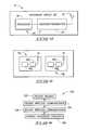
- Device 10includes a microelectronic package 12 which provides a housing within which integrated circuitry is received.
- microelectronic packagewill be understood to mean a housing or container within which integrated circuitry is received to provide a microelectronic device.
- example microelectronic packagesinclude product containers such as computer hard drive housings, cellular phone housings, and other hand-held electronic device housings. Such microelectronic packages need not, however, be hand-held.
- microelectronic packagescan include self-contained hermetically-sealed packages such as those which conventionally contain integrated circuit die. Such packages can be formed from plastic, ceramic, or any other suitable material.
- package 12has been broken away for clarity.
- An integrated circuit die 14is received within microelectronic package 12 and has integrated circuitry formed thereon.
- package 12includes individual die 16 , 18 , 20 , and 22 which have been prepackaged into individual respective integrated circuit chips which contain integrated circuitry which can be or is electrically connected into an operative arrangement.
- FIG. 2a top plan view of die 14 , 16 is shown.
- the dashed lines which bound the individual dieare intended to represent the exterior of a die or chip container.
- one of the integrated circuit diee.g. die 14
- Second transmit/receive circuitry(such as circuitry 26 ) is provided which is preferably discrete from first transmit/receive circuitry 26 .
- Such second transmit/receive circuitrycan be received or supported by die 16 . Accordingly, the second transmit/receive circuitry is contained within microelectronic package 12 and is configured to transmit and receive radio frequency signals.
- first and second transmit/receive circuitry 26are configured to establish wireless communication between one another within the microelectronic package.
- second transmit/receive circuitry(such as circuitry 26 b in FIG. 5) is disposed on a second integrated circuit die such as die 14 b .
- the microelectronic devicefurther includes a substrate 30 (FIGS. 1 and 2) disposed within the housing and supporting the first and second transmit/receive circuitry 26 . Any suitable material can be used for substrate 30 with exemplary substrates including a printed circuit board.
- microelectronic devicescan be provided which are small in size, such as those which can be hand-carried or transported.
- the integrated circuitry comprising the first and second transmit/receive circuitry 26are disposed within 24 inches of one another (distance d in FIG. 2) within the microelectronic package.
- integrated circuitry 24 comprising the first and second transmit/receive circuitry 26 respectivelycomprise individual respective antennas 32 (FIG. 5) which are configured to transmit and receive wireless communication.
- the antennascan be connected to their respective integrated circuitry 24 by a conductive trace of material (indicated as a dashed line extending between integrated circuitry 24 and antenna 32 in FIG. 3) over the die. Further augmentation can be provided by connecting the antenna to a lead finger, similar to lead fingers 34 , 36 (FIG. 3) via a wire bond.
- the antennasare configured to transmit and receive wireless RF communication.
- antennas 32are disposed within 24 inches of one another within the microelectronic package. In another embodiment, the antennas are disposed within one inch of one another within the microelectronic package. In yet another embodiment, the antennas are disposed within one-half inch of one another within the microelectronic package.
- die 14is void of external electrical connections for anything other than at least one of power and ground.
- lead fingers 34 , 36are provided and are coupled electrically with die 14 via wire bonds 38 , 40 respectively.
- the wire bondsconnect with contact pads 42 , 44 respectively on die 14 and provide the connections through which power and ground are established.
- These connectionsin this example, constitute the only connections which are necessarily made through lead fingers to the outside world. Of course, other connections can be made through lead fingers which are not specifically illustrated.
- an integrated circuit die 14is received within microelectronic package 12 and has integrated circuitry 24 thereon which is configured to operate in a designed manner.
- integrated circuitry 24includes a processor 46 (FIG. 4 ), 46 a , 46 b (FIG. 5 ).
- Processor 46can comprise any suitably formed or provided processor, e.g. a microprocessor, which is conventionally employed in integrated circuitry devices.
- FIG. 4also shows integrated circuitry 24 as including a receiver/transmitter 26 . Although this element is shown as a combination receiver/transmitter, it can comprise only a receiver or only a transmitter.
- FIG. 5shows an exemplary device which comprises two die 14 a , 14 b . These die are preferably part of and received inside of microelectronic package 12 .
- An integrated circuitry transmitter 26 ais provided and received within microelectronic package 12 .
- the transmittercan, but need not have a companion receiver.
- the transmitteris preferably configured to transmit wireless communication.
- An integrated circuitry receiver 26 bis provided and is received within microelectronic package 12 .
- the receivercan, but need not have a companion transmitter.
- Receiver 26 bis preferably configured to receive wireless communication which is transmitted by integrated circuitry transmitter 26 a .
- receiver 26 bis operably coupled with a processor 46 b and configured to provide data to the processor responsive to received wireless communication.
- receiver 26 bcomprises a portion of the integrated circuitry which is formed on die 14 b .
- integrated circuitry transmitter 26 ais disposed on a second integrated circuit die.
- more than one dieis received within the housing, as shown best in FIG. 1 .
- the plurality of dieall may or may not be configured to communicate with one another.
- die 14 a , 14 bare configured in some applications to establish wireless communication between them in a manner which serves to eliminate most, if not all physical-electrical connections which were formerly employed to establish wireless communication therebetween.
- individual diewere connected, via suitable wire bonds, to lead frames which, in turn, established electrical communication with the outside world.
- lead frameswhich, in turn, established electrical communication with the outside world.
- many of the wire bonds and lead fingers on the lead framescan be eliminated because now, functional communication between the separate die takes place through the transmission of wireless communication.
- physical-electrical connectioncan be provided in order to supply desired die with suitable power and ground connections.
- the transmitter and the receiverare disposed within the microelectronic package within 24 inches of one another. In another embodiment, the transmitter and the receiver are disposed within the microelectronic package within one inch of one another. In another embodiment, the transmitter and receiver are disposed within the microelectronic package within one-half inch of one another.
- processor 46is configured to receive data which is provided by receiver 26 and, responsive thereto, cause the integrated circuitry on die 14 to operate in the above-mentioned designed manner.
- the microelectronic device 10is hand-transportable.
- a microelectronic deviceincludes a microelectronic package 12 which provides a housing within which integrated circuitry is received.
- the microelectronic packagepreferably includes an integrated circuitry-supporting substrate 30 inside the housing.
- An integrated circuit diee.g. any and/or all of die 14 - 22 , is received within package 12 and supported by substrate 30 .
- the diepreferably has integrated circuitry formed thereon comprising first transmit/receive circuitry 26 a (FIG. 5) configured to transmit and receive wireless communication.
- Second transmit/receive circuitry 26 bis provided and is preferably discrete from first transmit/receive circuitry 26 a .
- the second transmit/receive circuitry 26 bis preferably contained within microelectronic package 12 and is configured to transmit and receive wireless communication.
- the first and second transmit/receive circuitry 26 a , 26 bare configured to establish wireless communication between one another within the microelectronic package 12 sufficient to enable the integrated circuitry on die 14 to operate in a designed manner.
- the second transmit/receive circuitryis supported by the integrated circuit-supporting substrate 30 .
- the second transmit/receive circuitry 26 bis disposed on a second integrated circuit die supported by the integrated circuitry-supporting substrate 30 .
- device 10is hand-transportable.
- individual antennas 32are provided and are operably associated with the first and second transmit/receive circuitry 26 a , 26 b respectively.
- the antennasare disposed within 24 inches of one another.
- the antennasare disposed within one inch of one another.
- the antennasare disposed within one-half inch of one another.
- a method of operating a microelectronic deviceis shown generally at 100 and includes at 102 , providing a microelectronic package having housed therein integrated circuitry.
- wireless communicationis produced using a transmitter inside of the microelectronic package.
- the produced wireless communicationis received using a receiver inside the microelectronic package.
- the integrated circuitry within the microelectronic packageis caused to operate in a designed manner.
- the production of wireless communication at 104takes place through the use of an integrated circuitry transmitter.
- the receipt of such wireless communicationtakes place through the use of an integrated circuitry receiver.
- Other embodimentsfurther comprise positioning the transmitter and the receiver inside the microelectronic package within 24 inches, one inch, and one-half inch respectively, of one another.
- provision of the integrated circuitry within the microelectronic packagecomprises fabricating the circuitry.
- a method of operating a microelectronic deviceincludes, at 202 , providing a microelectronic package having housed therein integrated circuitry.
- a wireless communication signalis transmitted using an integrated circuitry transmitter inside the microelectronic package.
- the transmitted wireless communication signalis received using an integrated circuitry receiver inside the microelectronic package.
- the integrated circuitry within the microelectronic packageis caused to operate in a designed manner.
- the transmitter and the receiverare positioned within 24 inches of one another. In other embodiments, the transmitter and the receiver are positioned within one inch and one-half inch respectively, of one another. Further aspects of the invention include fabricating one of the integrated circuitry transmitter or receiver, or preferably both.
- a method of providing a microelectronic deviceis shown generally at 300 and includes at 302 providing a microelectronic package within which integrated circuitry is to be housed.
- an integrated circuitry transmitteris mounted within the package.
- an integrated circuit dieis mounted within the package and includes integrated circuitry disposed thereon.
- the integrated circuitrypreferably includes an integrated circuit receiver, wherein the transmitter and the receiver are configured to establish direct wireless communication with one another.
- the wireless communicationpermits operating instructions for the integrated circuitry on the die to be transmitted and received within the microelectronic package.
- the transmitter and the receiverare mounted within 24 inches of one another.
- the transmitter and the receiverare mounted within one inch of one another.
- the transmitter and the receiverare mounted within one-half inch of one another.
- an exemplary microelectronic deviceis shown generally at 50 and includes a microelectronic package 52 .
- Package 52contains and supports an integrated circuit die 54 .
- Physical-electrical connection structureis provided and shown generally at 56 , and secures die 54 to an integrated circuitry-supporting substrate 58 .
- the physical-electrical connection structureprovides both electrical and physical connections between circuit die 54 and outside world circuitry.
- physical-electrical connection structure 56supplies electrical connections only for power and ground.
- the physical-electrical connection structureincludes respective wire bonds 60 , 62 which are individually and respectively connected with lead fingers 64 , 66 .
- Advantages of various embodiments of the inventioninclude a reduction in the number wire bonds necessary to impart functionality to a microelectronic device.
- the number of processing steps which are needed to ensure that wire bonds are adequately formed between a lead frame and bond pads on an integrated circuit diecan be reduced.
- risks which were formerly associated with wire bonds becoming detached because of the very thin nature of such connectionscan be reduced.
- Various embodiments of the inventioncan provide improved microelectronic devices and methods of forming the same which reduce processing complexities and provide for improved performance.
Landscapes
- Engineering & Computer Science (AREA)
- Microelectronics & Electronic Packaging (AREA)
- Power Engineering (AREA)
- Physics & Mathematics (AREA)
- Condensed Matter Physics & Semiconductors (AREA)
- General Physics & Mathematics (AREA)
- Computer Hardware Design (AREA)
- Computer Networks & Wireless Communication (AREA)
- Signal Processing (AREA)
- Semiconductor Integrated Circuits (AREA)
Abstract
Description
Claims (35)
Priority Applications (6)
| Application Number | Priority Date | Filing Date | Title |
|---|---|---|---|
| US10/371,123US6718163B2 (en) | 1999-03-01 | 2003-02-19 | Methods of operating microelectronic devices, and methods of providing microelectronic devices |
| US10/793,173US7107019B2 (en) | 1999-03-01 | 2004-03-03 | Methods of operating microelectronic devices, and methods of providing microelectronic devices |
| US11/512,783US7593708B2 (en) | 1999-03-01 | 2006-08-29 | Methods of operating electronic devices, and methods of providing electronic devices |
| US11/847,645US7778621B2 (en) | 1999-03-01 | 2007-08-30 | Methods of operating electronic devices, and methods of providing electronic devices |
| US12/853,783US8036629B2 (en) | 1999-03-01 | 2010-08-10 | Methods of operating electronic devices, and methods of providing electronic devices |
| US13/269,820US8554166B2 (en) | 1999-03-01 | 2011-10-10 | Methods of operating electronic devices, and methods of providing electronic devices |
Applications Claiming Priority (2)
| Application Number | Priority Date | Filing Date | Title |
|---|---|---|---|
| US09/260,997US6542720B1 (en) | 1999-03-01 | 1999-03-01 | Microelectronic devices, methods of operating microelectronic devices, and methods of providing microelectronic devices |
| US10/371,123US6718163B2 (en) | 1999-03-01 | 2003-02-19 | Methods of operating microelectronic devices, and methods of providing microelectronic devices |
Related Parent Applications (1)
| Application Number | Title | Priority Date | Filing Date |
|---|---|---|---|
| US09/260,997ContinuationUS6542720B1 (en) | 1999-03-01 | 1999-03-01 | Microelectronic devices, methods of operating microelectronic devices, and methods of providing microelectronic devices |
Related Child Applications (1)
| Application Number | Title | Priority Date | Filing Date |
|---|---|---|---|
| US10/793,173ContinuationUS7107019B2 (en) | 1999-03-01 | 2004-03-03 | Methods of operating microelectronic devices, and methods of providing microelectronic devices |
Publications (2)
| Publication Number | Publication Date |
|---|---|
| US20030129951A1 US20030129951A1 (en) | 2003-07-10 |
| US6718163B2true US6718163B2 (en) | 2004-04-06 |
Family
ID=22991537
Family Applications (7)
| Application Number | Title | Priority Date | Filing Date |
|---|---|---|---|
| US09/260,997Expired - Fee RelatedUS6542720B1 (en) | 1999-03-01 | 1999-03-01 | Microelectronic devices, methods of operating microelectronic devices, and methods of providing microelectronic devices |
| US10/371,123Expired - Fee RelatedUS6718163B2 (en) | 1999-03-01 | 2003-02-19 | Methods of operating microelectronic devices, and methods of providing microelectronic devices |
| US10/793,173Expired - Fee RelatedUS7107019B2 (en) | 1999-03-01 | 2004-03-03 | Methods of operating microelectronic devices, and methods of providing microelectronic devices |
| US11/512,783Expired - Fee RelatedUS7593708B2 (en) | 1999-03-01 | 2006-08-29 | Methods of operating electronic devices, and methods of providing electronic devices |
| US11/847,645Expired - Fee RelatedUS7778621B2 (en) | 1999-03-01 | 2007-08-30 | Methods of operating electronic devices, and methods of providing electronic devices |
| US12/853,783Expired - Fee RelatedUS8036629B2 (en) | 1999-03-01 | 2010-08-10 | Methods of operating electronic devices, and methods of providing electronic devices |
| US13/269,820Expired - Fee RelatedUS8554166B2 (en) | 1999-03-01 | 2011-10-10 | Methods of operating electronic devices, and methods of providing electronic devices |
Family Applications Before (1)
| Application Number | Title | Priority Date | Filing Date |
|---|---|---|---|
| US09/260,997Expired - Fee RelatedUS6542720B1 (en) | 1999-03-01 | 1999-03-01 | Microelectronic devices, methods of operating microelectronic devices, and methods of providing microelectronic devices |
Family Applications After (5)
| Application Number | Title | Priority Date | Filing Date |
|---|---|---|---|
| US10/793,173Expired - Fee RelatedUS7107019B2 (en) | 1999-03-01 | 2004-03-03 | Methods of operating microelectronic devices, and methods of providing microelectronic devices |
| US11/512,783Expired - Fee RelatedUS7593708B2 (en) | 1999-03-01 | 2006-08-29 | Methods of operating electronic devices, and methods of providing electronic devices |
| US11/847,645Expired - Fee RelatedUS7778621B2 (en) | 1999-03-01 | 2007-08-30 | Methods of operating electronic devices, and methods of providing electronic devices |
| US12/853,783Expired - Fee RelatedUS8036629B2 (en) | 1999-03-01 | 2010-08-10 | Methods of operating electronic devices, and methods of providing electronic devices |
| US13/269,820Expired - Fee RelatedUS8554166B2 (en) | 1999-03-01 | 2011-10-10 | Methods of operating electronic devices, and methods of providing electronic devices |
Country Status (1)
| Country | Link |
|---|---|
| US (7) | US6542720B1 (en) |
Cited By (47)
| Publication number | Priority date | Publication date | Assignee | Title |
|---|---|---|---|---|
| US20040053584A1 (en)* | 2002-09-18 | 2004-03-18 | Mickle Marlin H. | Recharging method and apparatus |
| US20040256722A1 (en)* | 1999-03-01 | 2004-12-23 | Tandy Patrick W. | Methods of operating microelectronic devices, and methods of providing microelectronic devices |
| US20040266382A1 (en)* | 2003-06-30 | 2004-12-30 | Infineon Technologies Ag | Method for wireless data interchange between circuit units within a package, and circuit arrangement for performing the method |
| US20050110615A1 (en)* | 2003-11-21 | 2005-05-26 | Matsushita Electric Industrial Co., Ltd. | Radio communications medium processing unit |
| US20060172719A1 (en)* | 2005-01-31 | 2006-08-03 | Ker-Min Chen | Method and apparatus for inter-chip wireless communication |
| WO2006055547A3 (en)* | 2004-11-15 | 2006-08-24 | Izex Technologies Inc | Instrumented orthopedic and other medical implants |
| US20060211449A1 (en)* | 2005-03-18 | 2006-09-21 | Honeywell International Inc. | Reconfigurable wireless interconnects for data communication |
| US20060223456A1 (en)* | 2005-03-31 | 2006-10-05 | Ouzillou Mendy M | Techniques for partitioning radios in wireless communication systems |
| US20060223577A1 (en)* | 2005-03-31 | 2006-10-05 | Ouzillou Mendy M | Techniques for partitioning radios in wireless communication systems |
| US20070010282A1 (en)* | 2005-06-23 | 2007-01-11 | Dates Eric T | Cellular telephone system improvement - known as the "007 WEB" |
| US20070155588A1 (en)* | 1998-09-01 | 2007-07-05 | Izex Technologies, Inc. | Remote monitoring of a patient |
| US20070207734A1 (en)* | 2006-02-17 | 2007-09-06 | International Rectifier Corporation | Wireless communication between control devices and controlled devices within a common board and rf high side coupler with plane polarized antenna |
| WO2007126910A1 (en)* | 2006-03-31 | 2007-11-08 | Intel Corporation | A single package wireless communication device |
| US20100121160A1 (en)* | 1999-06-23 | 2010-05-13 | Izex Technologies, Inc. | Remote psychological evaluation |
| US20100159829A1 (en)* | 2008-12-23 | 2010-06-24 | Mccormack Gary D | Tightly-coupled near-field communication-link connector-replacement chips |
| US20100201587A1 (en)* | 2006-12-29 | 2010-08-12 | Broadcom Corporation | Integrated circuit mems antenna structure |
| US7953427B1 (en)* | 2004-02-19 | 2011-05-31 | Marvell International, Ltd. | Communication access apparatus systems, and methods |
| US8308794B2 (en) | 2004-11-15 | 2012-11-13 | IZEK Technologies, Inc. | Instrumented implantable stents, vascular grafts and other medical devices |
| US8714459B2 (en) | 2011-05-12 | 2014-05-06 | Waveconnex, Inc. | Scalable high-bandwidth connectivity |
| US8794980B2 (en) | 2011-12-14 | 2014-08-05 | Keyssa, Inc. | Connectors providing HAPTIC feedback |
| US8811526B2 (en) | 2011-05-31 | 2014-08-19 | Keyssa, Inc. | Delta modulated low power EHF communication link |
| US8897700B2 (en) | 2011-06-15 | 2014-11-25 | Keyssa, Inc. | Distance measurement using EHF signals |
| US8909135B2 (en) | 2011-09-15 | 2014-12-09 | Keyssa, Inc. | Wireless communication with dielectric medium |
| US8929834B2 (en) | 2012-03-06 | 2015-01-06 | Keyssa, Inc. | System for constraining an operating parameter of an EHF communication chip |
| US20150053770A1 (en)* | 2013-08-22 | 2015-02-26 | Texas Instruments Deutschland Gmbh | Rfid tag with integrated antenna |
| US9191263B2 (en) | 2008-12-23 | 2015-11-17 | Keyssa, Inc. | Contactless replacement for cabled standards-based interfaces |
| US9203597B2 (en) | 2012-03-02 | 2015-12-01 | Keyssa, Inc. | Systems and methods for duplex communication |
| US9219956B2 (en) | 2008-12-23 | 2015-12-22 | Keyssa, Inc. | Contactless audio adapter, and methods |
| US9374154B2 (en) | 2012-09-14 | 2016-06-21 | Keyssa, Inc. | Wireless connections with virtual hysteresis |
| US9379450B2 (en) | 2011-03-24 | 2016-06-28 | Keyssa, Inc. | Integrated circuit with electromagnetic communication |
| US9407311B2 (en) | 2011-10-21 | 2016-08-02 | Keyssa, Inc. | Contactless signal splicing using an extremely high frequency (EHF) communication link |
| US9426660B2 (en) | 2013-03-15 | 2016-08-23 | Keyssa, Inc. | EHF secure communication device |
| US9474099B2 (en) | 2008-12-23 | 2016-10-18 | Keyssa, Inc. | Smart connectors and associated communications links |
| US9515365B2 (en) | 2012-08-10 | 2016-12-06 | Keyssa, Inc. | Dielectric coupling systems for EHF communications |
| US9531425B2 (en) | 2012-12-17 | 2016-12-27 | Keyssa, Inc. | Modular electronics |
| US9553353B2 (en) | 2012-03-28 | 2017-01-24 | Keyssa, Inc. | Redirection of electromagnetic signals using substrate structures |
| US9553616B2 (en) | 2013-03-15 | 2017-01-24 | Keyssa, Inc. | Extremely high frequency communication chip |
| US9559790B2 (en) | 2012-01-30 | 2017-01-31 | Keyssa, Inc. | Link emission control |
| US9614590B2 (en) | 2011-05-12 | 2017-04-04 | Keyssa, Inc. | Scalable high-bandwidth connectivity |
| US9705204B2 (en) | 2011-10-20 | 2017-07-11 | Keyssa, Inc. | Low-profile wireless connectors |
| US9853746B2 (en) | 2012-01-30 | 2017-12-26 | Keyssa, Inc. | Shielded EHF connector assemblies |
| US9954579B2 (en) | 2008-12-23 | 2018-04-24 | Keyssa, Inc. | Smart connectors and associated communications links |
| US9960820B2 (en) | 2008-12-23 | 2018-05-01 | Keyssa, Inc. | Contactless data transfer systems and methods |
| US10049801B2 (en) | 2015-10-16 | 2018-08-14 | Keyssa Licensing, Inc. | Communication module alignment |
| US10305196B2 (en) | 2012-04-17 | 2019-05-28 | Keyssa, Inc. | Dielectric lens structures for EHF radiation |
| US10375221B2 (en) | 2015-04-30 | 2019-08-06 | Keyssa Systems, Inc. | Adapter devices for enhancing the functionality of other devices |
| US11176338B1 (en)* | 2019-11-01 | 2021-11-16 | Bae Systems Information And Electronic Systems Integration Inc. | On-chip RF interrogation for heterogeneous RFIDS |
Families Citing this family (46)
| Publication number | Priority date | Publication date | Assignee | Title |
|---|---|---|---|---|
| GB2367691B (en)* | 2000-09-29 | 2005-05-18 | Roke Manor Research | Processor array having sub-function nodes with antennas for radio communication with other sub-function nodes. |
| US7501954B1 (en)* | 2000-10-11 | 2009-03-10 | Avante International Technology, Inc. | Dual circuit RF identification tags |
| DE10202480A1 (en)* | 2001-01-30 | 2002-08-14 | Infineon Technologies Ag | Signal transfer method for computer, involves converting signal into line-independent electromagnetic wave at transmitter in one electronic module, which is reconverted into reception signal at receiver of other module |
| US6856788B2 (en)* | 2001-04-20 | 2005-02-15 | Mastek International | Wireless IC interconnection method and system |
| US6563185B2 (en)* | 2001-05-21 | 2003-05-13 | The Regents Of The University Of Colorado | High speed electron tunneling device and applications |
| US6967347B2 (en)* | 2001-05-21 | 2005-11-22 | The Regents Of The University Of Colorado | Terahertz interconnect system and applications |
| US7177515B2 (en)* | 2002-03-20 | 2007-02-13 | The Regents Of The University Of Colorado | Surface plasmon devices |
| US7126151B2 (en)* | 2001-05-21 | 2006-10-24 | The Regents Of The University Of Colorado, A Body Corporate | Interconnected high speed electron tunneling devices |
| JP3941620B2 (en)* | 2001-08-31 | 2007-07-04 | 株式会社デンソーウェーブ | Electronic device with built-in ID tag |
| US6993298B2 (en)* | 2001-09-07 | 2006-01-31 | Siemens Energy & Automation, Inc. | Programmable controller with RF wireless interface |
| JP4848108B2 (en)* | 2001-09-14 | 2011-12-28 | インターナショナル・ビジネス・マシーンズ・コーポレーション | Data processing system |
| US7383058B2 (en)* | 2002-07-16 | 2008-06-03 | Intel Corporation | RF/microwave system with a system on a chip package or the like |
| US7112884B2 (en) | 2002-08-23 | 2006-09-26 | Ati Technologies, Inc. | Integrated circuit having memory disposed thereon and method of making thereof |
| US7088964B2 (en)* | 2002-10-02 | 2006-08-08 | University Of Florida Research Foundation, Inc. | Single chip radio with integrated antenna |
| US7590397B2 (en)* | 2003-09-10 | 2009-09-15 | Sony Corporation | Signal processing apparatus and signal processing method, program, and recording medium |
| US7667974B2 (en)* | 2004-01-28 | 2010-02-23 | Panasonic Corporation | Module and mounted structure using the same |
| US7769355B2 (en)* | 2005-01-19 | 2010-08-03 | Micro Mobio Corporation | System-in-package wireless communication device comprising prepackaged power amplifier |
| CN1949686A (en)* | 2005-10-14 | 2007-04-18 | 鸿富锦精密工业(深圳)有限公司 | System and method for transmitting signal between IC |
| DE102006061586B4 (en)* | 2006-12-27 | 2009-01-08 | Fraunhofer-Gesellschaft zur Förderung der angewandten Forschung e.V. | Connection network between semiconductor structures and thus equipped circuit and method for data transmission |
| US7890064B1 (en)* | 2006-12-30 | 2011-02-15 | Broadcom Corporation | Multi-path transceiver layout within a device |
| US8149818B2 (en)* | 2006-12-30 | 2012-04-03 | Broadcom Corporation | Mesh network within a device |
| US7974587B2 (en)* | 2006-12-30 | 2011-07-05 | Broadcom Corporation | Local wireless communications within a device |
| US7809329B2 (en)* | 2007-01-31 | 2010-10-05 | Broadcom Corporation | Shared RF bus structure |
| JP4837776B2 (en)* | 2007-03-29 | 2011-12-14 | 京セラ株式会社 | Portable radio |
| WO2008120756A1 (en)* | 2007-03-29 | 2008-10-09 | Kyocera Corporation | Portable wireless device |
| US8064967B2 (en)* | 2007-08-01 | 2011-11-22 | Broadcom Corporation | Wireless connection integrated circuit (IC) having power island(s) |
| US8385869B2 (en)* | 2007-11-07 | 2013-02-26 | Qualcomm, Incorporated | Embedded module receiver noise profiling |
| US8384596B2 (en)* | 2008-06-19 | 2013-02-26 | Broadcom Corporation | Method and system for inter-chip communication via integrated circuit package antennas |
| US9083573B2 (en)* | 2008-10-15 | 2015-07-14 | Stmicroelectronics Asia Pacific Pte. Ltd. | Simultaneous transmission of signals, such as orthogonal-frequency-division-multiplexed (OFDM) signals, that include a same frequency |
| US9130789B2 (en)* | 2008-10-15 | 2015-09-08 | Stmicroelectronics Asia Pacific Pte. Ltd. | Recovering data from a secondary one of simultaneous signals, such as orthogonal-frequency-division-multiplexed (OFDM) signals, that include a same frequency |
| US9338033B2 (en) | 2008-10-15 | 2016-05-10 | Stmicroelectronics, Inc. | Recovering data from a primary one of simultaneous signals, such as orthogonal-frequency-division-multiplexed (OFDM) signals, that include a same frequency |
| US8401598B2 (en)* | 2009-05-11 | 2013-03-19 | Broadcom Corporation | Method and system for chip to chip communication utilizing selectable directional antennas |
| US8295788B2 (en)* | 2009-06-09 | 2012-10-23 | Broadcom Corporation | Method and system for an N-phase transmitter utilizing a leaky wave antenna |
| DK2585378T3 (en)* | 2010-06-22 | 2019-11-11 | Stora Enso Oyj | FIBER OR PLASTIC BASKET, DEVICE, PROCEDURE, PROGRAM AND SYSTEM FOR WIRELESS DATA COMMUNICATION THROUGH FIBER OR PLASTIC BASKET |
| US20110316139A1 (en)* | 2010-06-23 | 2011-12-29 | Broadcom Corporation | Package for a wireless enabled integrated circuit |
| US20120086114A1 (en)* | 2010-10-07 | 2012-04-12 | Broadcom Corporation | Millimeter devices on an integrated circuit |
| JP2012089997A (en)* | 2010-10-18 | 2012-05-10 | Sony Corp | Signal transmission device, electronic apparatus, and signal transmission method |
| US8901945B2 (en) | 2011-02-23 | 2014-12-02 | Broadcom Corporation | Test board for use with devices having wirelessly enabled functional blocks and method of using same |
| US8928139B2 (en) | 2011-09-30 | 2015-01-06 | Broadcom Corporation | Device having wirelessly enabled functional blocks |
| US8671171B2 (en) | 2011-12-01 | 2014-03-11 | International Business Machines Corporation | Wireless configuration for a computing device |
| JP5726787B2 (en)* | 2012-02-28 | 2015-06-03 | 株式会社東芝 | Wireless device, information processing device and storage device provided with the same |
| JP5710558B2 (en) | 2012-08-24 | 2015-04-30 | 株式会社東芝 | Wireless device, information processing device and storage device including the same |
| EP2974058B1 (en) | 2013-03-15 | 2020-07-15 | Keyssa, Inc. | Contactless ehf data communication |
| WO2015058203A1 (en) | 2013-10-18 | 2015-04-23 | Keyssa, Inc. | Contactless communication unit connector assemblies with signal directing structures |
| US9160465B2 (en) | 2013-11-07 | 2015-10-13 | Silicon Labortories Inc. | Spur cancellation systems and related methods |
| US9252891B2 (en)* | 2013-11-07 | 2016-02-02 | Silicon Laboratories Inc. | Die-to-die communication links for receiver integrated circuit dies and related methods |
Citations (40)
| Publication number | Priority date | Publication date | Assignee | Title |
|---|---|---|---|---|
| US3651434A (en) | 1969-04-30 | 1972-03-21 | Microwave Semiconductor Corp | Microwave package for holding a microwave device, particularly for strip transmission line use, with reduced input-output coupling |
| US3936864A (en) | 1973-05-18 | 1976-02-03 | Raytheon Company | Microwave transistor package |
| US5117068A (en) | 1990-08-17 | 1992-05-26 | Watkins-Johnson Company | Surface mount package for R.F. devices |
| US5313211A (en) | 1990-08-13 | 1994-05-17 | Sharp Kabushiki Kaisha | Portable data processing device capable of transmitting processed data on a radio by reflection of unmodulated carrier signal externally applied |
| US5337063A (en) | 1991-04-22 | 1994-08-09 | Mitsubishi Denki Kabushiki Kaisha | Antenna circuit for non-contact IC card and method of manufacturing the same |
| US5340968A (en) | 1991-05-07 | 1994-08-23 | Nippondenso Company, Ltd. | Information storage medium with electronic and visual areas |
| US5347263A (en) | 1993-02-05 | 1994-09-13 | Gnuco Technology Corporation | Electronic identifier apparatus and method utilizing a single chip microcontroller and an antenna coil |
| US5497140A (en) | 1992-08-12 | 1996-03-05 | Micron Technology, Inc. | Electrically powered postage stamp or mailing or shipping label operative with radio frequency (RF) communication |
| US5563086A (en) | 1993-09-13 | 1996-10-08 | International Business Machines Corporation | Integrated memory cube, structure and fabrication |
| US5621913A (en)* | 1992-05-15 | 1997-04-15 | Micron Technology, Inc. | System with chip to chip communication |
| US5692298A (en) | 1993-10-08 | 1997-12-02 | Stratedge Corporation | Method of making ceramic microwave electronic package |
| US5734198A (en) | 1994-11-10 | 1998-03-31 | Micron Technology, Inc. | Multi-layer lead frame for a semiconductor device |
| US5736783A (en) | 1993-10-08 | 1998-04-07 | Stratedge Corporation. | High frequency microelectronics package |
| US5751820A (en)* | 1997-04-02 | 1998-05-12 | Resound Corporation | Integrated circuit design for a personal use wireless communication system utilizing reflection |
| US5754948A (en)* | 1995-12-29 | 1998-05-19 | University Of North Carolina At Charlotte | Millimeter-wave wireless interconnection of electronic components |
| US5757074A (en)* | 1995-07-07 | 1998-05-26 | Hughes Electronics Corporation | Microwave/millimeter wave circuit structure with discrete flip-chip mounted elements |
| US5763945A (en) | 1996-09-13 | 1998-06-09 | Micron Technology, Inc. | Integrated circuit package electrical enhancement with improved lead frame design |
| US5818105A (en)* | 1994-07-22 | 1998-10-06 | Nec Corporation | Semiconductor device with plastic material covering a semiconductor chip mounted on a substrate of the device |
| US5842118A (en) | 1996-12-18 | 1998-11-24 | Micron Communications, Inc. | Communication system including diversity antenna queuing |
| US5903050A (en) | 1998-04-30 | 1999-05-11 | Lsi Logic Corporation | Semiconductor package having capacitive extension spokes and method for making the same |
| US5903168A (en) | 1997-03-21 | 1999-05-11 | Industrial Technology Research Institiute | Switchable MCM CMOS I/O buffers |
| US6031459A (en)* | 1998-07-22 | 2000-02-29 | Micron Technology, Inc. | Wireless communication devices, radio frequency identification devices, and methods of forming wireless communication devices and radio frequency identification devices |
| US6060342A (en)* | 1998-04-06 | 2000-05-09 | P-Com, Incorporated | Circuit packaging for millimeter-wave components |
| US6078791A (en)* | 1992-06-17 | 2000-06-20 | Micron Communications, Inc. | Radio frequency identification transceiver and antenna |
| JP2000223656A (en) | 1999-02-03 | 2000-08-11 | Rohm Co Ltd | Semiconductor device for radio communication device and radio communication device using the same |
| US6140697A (en)* | 1995-05-18 | 2000-10-31 | Hitachi, Ltd. | Semiconductor device |
| US6169295B1 (en) | 1998-05-29 | 2001-01-02 | Maxim Integrated Products, Inc. | Infrared transceiver module and method for making same |
| US6168084B1 (en)* | 1997-08-19 | 2001-01-02 | Micron Technology, Inc. | Wireless communication devices and methods of forming wireless communication devices |
| US6172425B1 (en) | 1995-04-28 | 2001-01-09 | Telefonaktiebolaget Lm Ericsson (Publ) | Encapsulation of transmitter and receiver modules |
| US6170748B1 (en) | 1997-01-06 | 2001-01-09 | Widata Corporation | Object identification system employing pulsed magnetic field-stimulated, tag-embedded transponder |
| US6175124B1 (en) | 1998-06-30 | 2001-01-16 | Lsi Logic Corporation | Method and apparatus for a wafer level system |
| US6180433B1 (en) | 1997-09-15 | 2001-01-30 | Microchip Technology Incorporated | Combination inductive coil and integrated circuit semiconductor chip in a single lead frame package and method therefor |
| US6184060B1 (en) | 1996-10-29 | 2001-02-06 | Trusi Technologies Llc | Integrated circuits and methods for their fabrication |
| US6263193B1 (en)* | 1997-03-28 | 2001-07-17 | Kabushiki Kaisha Toshiba | Microwave transmitter/receiver module |
| US6335669B1 (en)* | 1998-12-09 | 2002-01-01 | Mitsubishi Denki Kabushiki Kaisha | RF circuit module |
| US6480699B1 (en)* | 1998-08-28 | 2002-11-12 | Woodtoga Holdings Company | Stand-alone device for transmitting a wireless signal containing data from a memory or a sensor |
| US6496889B1 (en)* | 1999-09-17 | 2002-12-17 | Rambus Inc. | Chip-to-chip communication system using an ac-coupled bus and devices employed in same |
| US6542720B1 (en)* | 1999-03-01 | 2003-04-01 | Micron Technology, Inc. | Microelectronic devices, methods of operating microelectronic devices, and methods of providing microelectronic devices |
| US6563464B2 (en)* | 2001-03-19 | 2003-05-13 | International Business Machines Corporation | Integrated on-chip half-wave dipole antenna structure |
| US6646554B1 (en)* | 1998-06-08 | 2003-11-11 | 3M Innovative Properties Company | Identification tag with enhanced security |
Family Cites Families (20)
| Publication number | Priority date | Publication date | Assignee | Title |
|---|---|---|---|---|
| JP3115095B2 (en)* | 1992-04-20 | 2000-12-04 | ディップソール株式会社 | Electroless plating solution and plating method using the same |
| US5797140A (en)* | 1992-11-25 | 1998-08-25 | Second Chance Body Armor, Inc. | Ballistic resistant garment assembly and method of using the same |
| US6728113B1 (en) | 1993-06-24 | 2004-04-27 | Polychip, Inc. | Method and apparatus for non-conductively interconnecting integrated circuits |
| DE10202480A1 (en)* | 2001-01-30 | 2002-08-14 | Infineon Technologies Ag | Signal transfer method for computer, involves converting signal into line-independent electromagnetic wave at transmitter in one electronic module, which is reconverted into reception signal at receiver of other module |
| US6512431B2 (en)* | 2001-02-28 | 2003-01-28 | Lockheed Martin Corporation | Millimeterwave module compact interconnect |
| US6856788B2 (en)* | 2001-04-20 | 2005-02-15 | Mastek International | Wireless IC interconnection method and system |
| US7126151B2 (en)* | 2001-05-21 | 2006-10-24 | The Regents Of The University Of Colorado, A Body Corporate | Interconnected high speed electron tunneling devices |
| US6967347B2 (en)* | 2001-05-21 | 2005-11-22 | The Regents Of The University Of Colorado | Terahertz interconnect system and applications |
| JP3941620B2 (en)* | 2001-08-31 | 2007-07-04 | 株式会社デンソーウェーブ | Electronic device with built-in ID tag |
| JP4848108B2 (en)* | 2001-09-14 | 2011-12-28 | インターナショナル・ビジネス・マシーンズ・コーポレーション | Data processing system |
| US7383058B2 (en)* | 2002-07-16 | 2008-06-03 | Intel Corporation | RF/microwave system with a system on a chip package or the like |
| US7088964B2 (en)* | 2002-10-02 | 2006-08-08 | University Of Florida Research Foundation, Inc. | Single chip radio with integrated antenna |
| DE10329347B4 (en)* | 2003-06-30 | 2010-08-12 | Qimonda Ag | Method for wireless data exchange between circuit units within a housing and circuit arrangement for carrying out the method |
| WO2006055547A2 (en)* | 2004-11-15 | 2006-05-26 | Izex Technologies, Inc. | Instrumented orthopedic and other medical implants |
| US7769355B2 (en)* | 2005-01-19 | 2010-08-03 | Micro Mobio Corporation | System-in-package wireless communication device comprising prepackaged power amplifier |
| US7330702B2 (en)* | 2005-01-31 | 2008-02-12 | Taiwan Semiconductor Manufacturing Co., Ltd. | Method and apparatus for inter-chip wireless communication |
| US20070207734A1 (en)* | 2006-02-17 | 2007-09-06 | International Rectifier Corporation | Wireless communication between control devices and controlled devices within a common board and rf high side coupler with plane polarized antenna |
| US7692295B2 (en)* | 2006-03-31 | 2010-04-06 | Intel Corporation | Single package wireless communication device |
| US7809329B2 (en)* | 2007-01-31 | 2010-10-05 | Broadcom Corporation | Shared RF bus structure |
| US7768457B2 (en)* | 2007-06-22 | 2010-08-03 | Vubiq, Inc. | Integrated antenna and chip package and method of manufacturing thereof |
- 1999
- 1999-03-01USUS09/260,997patent/US6542720B1/ennot_activeExpired - Fee Related
- 2003
- 2003-02-19USUS10/371,123patent/US6718163B2/ennot_activeExpired - Fee Related
- 2004
- 2004-03-03USUS10/793,173patent/US7107019B2/ennot_activeExpired - Fee Related
- 2006
- 2006-08-29USUS11/512,783patent/US7593708B2/ennot_activeExpired - Fee Related
- 2007
- 2007-08-30USUS11/847,645patent/US7778621B2/ennot_activeExpired - Fee Related
- 2010
- 2010-08-10USUS12/853,783patent/US8036629B2/ennot_activeExpired - Fee Related
- 2011
- 2011-10-10USUS13/269,820patent/US8554166B2/ennot_activeExpired - Fee Related
Patent Citations (42)
| Publication number | Priority date | Publication date | Assignee | Title |
|---|---|---|---|---|
| US3651434A (en) | 1969-04-30 | 1972-03-21 | Microwave Semiconductor Corp | Microwave package for holding a microwave device, particularly for strip transmission line use, with reduced input-output coupling |
| US3936864A (en) | 1973-05-18 | 1976-02-03 | Raytheon Company | Microwave transistor package |
| US5313211A (en) | 1990-08-13 | 1994-05-17 | Sharp Kabushiki Kaisha | Portable data processing device capable of transmitting processed data on a radio by reflection of unmodulated carrier signal externally applied |
| US5117068A (en) | 1990-08-17 | 1992-05-26 | Watkins-Johnson Company | Surface mount package for R.F. devices |
| US5337063A (en) | 1991-04-22 | 1994-08-09 | Mitsubishi Denki Kabushiki Kaisha | Antenna circuit for non-contact IC card and method of manufacturing the same |
| US5340968A (en) | 1991-05-07 | 1994-08-23 | Nippondenso Company, Ltd. | Information storage medium with electronic and visual areas |
| US5621913A (en)* | 1992-05-15 | 1997-04-15 | Micron Technology, Inc. | System with chip to chip communication |
| US6078791A (en)* | 1992-06-17 | 2000-06-20 | Micron Communications, Inc. | Radio frequency identification transceiver and antenna |
| US5497140A (en) | 1992-08-12 | 1996-03-05 | Micron Technology, Inc. | Electrically powered postage stamp or mailing or shipping label operative with radio frequency (RF) communication |
| US6013949A (en) | 1992-08-12 | 2000-01-11 | Micron Technology, Inc. | Miniature Radio Frequency Transceiver |
| US5347263A (en) | 1993-02-05 | 1994-09-13 | Gnuco Technology Corporation | Electronic identifier apparatus and method utilizing a single chip microcontroller and an antenna coil |
| US5563086A (en) | 1993-09-13 | 1996-10-08 | International Business Machines Corporation | Integrated memory cube, structure and fabrication |
| US5736783A (en) | 1993-10-08 | 1998-04-07 | Stratedge Corporation. | High frequency microelectronics package |
| US5692298A (en) | 1993-10-08 | 1997-12-02 | Stratedge Corporation | Method of making ceramic microwave electronic package |
| US5818105A (en)* | 1994-07-22 | 1998-10-06 | Nec Corporation | Semiconductor device with plastic material covering a semiconductor chip mounted on a substrate of the device |
| US5734198A (en) | 1994-11-10 | 1998-03-31 | Micron Technology, Inc. | Multi-layer lead frame for a semiconductor device |
| US6172425B1 (en) | 1995-04-28 | 2001-01-09 | Telefonaktiebolaget Lm Ericsson (Publ) | Encapsulation of transmitter and receiver modules |
| US6140697A (en)* | 1995-05-18 | 2000-10-31 | Hitachi, Ltd. | Semiconductor device |
| US5757074A (en)* | 1995-07-07 | 1998-05-26 | Hughes Electronics Corporation | Microwave/millimeter wave circuit structure with discrete flip-chip mounted elements |
| US5754948A (en)* | 1995-12-29 | 1998-05-19 | University Of North Carolina At Charlotte | Millimeter-wave wireless interconnection of electronic components |
| US5763945A (en) | 1996-09-13 | 1998-06-09 | Micron Technology, Inc. | Integrated circuit package electrical enhancement with improved lead frame design |
| US6184060B1 (en) | 1996-10-29 | 2001-02-06 | Trusi Technologies Llc | Integrated circuits and methods for their fabrication |
| US5842118A (en) | 1996-12-18 | 1998-11-24 | Micron Communications, Inc. | Communication system including diversity antenna queuing |
| US6023610A (en) | 1996-12-18 | 2000-02-08 | Micron Technology, Inc. | Communication system including diversity antenna queuing |
| US6170748B1 (en) | 1997-01-06 | 2001-01-09 | Widata Corporation | Object identification system employing pulsed magnetic field-stimulated, tag-embedded transponder |
| US5903168A (en) | 1997-03-21 | 1999-05-11 | Industrial Technology Research Institiute | Switchable MCM CMOS I/O buffers |
| US6263193B1 (en)* | 1997-03-28 | 2001-07-17 | Kabushiki Kaisha Toshiba | Microwave transmitter/receiver module |
| US5751820A (en)* | 1997-04-02 | 1998-05-12 | Resound Corporation | Integrated circuit design for a personal use wireless communication system utilizing reflection |
| US6168084B1 (en)* | 1997-08-19 | 2001-01-02 | Micron Technology, Inc. | Wireless communication devices and methods of forming wireless communication devices |
| US6180433B1 (en) | 1997-09-15 | 2001-01-30 | Microchip Technology Incorporated | Combination inductive coil and integrated circuit semiconductor chip in a single lead frame package and method therefor |
| US6060342A (en)* | 1998-04-06 | 2000-05-09 | P-Com, Incorporated | Circuit packaging for millimeter-wave components |
| US5903050A (en) | 1998-04-30 | 1999-05-11 | Lsi Logic Corporation | Semiconductor package having capacitive extension spokes and method for making the same |
| US6169295B1 (en) | 1998-05-29 | 2001-01-02 | Maxim Integrated Products, Inc. | Infrared transceiver module and method for making same |
| US6646554B1 (en)* | 1998-06-08 | 2003-11-11 | 3M Innovative Properties Company | Identification tag with enhanced security |
| US6175124B1 (en) | 1998-06-30 | 2001-01-16 | Lsi Logic Corporation | Method and apparatus for a wafer level system |
| US6031459A (en)* | 1998-07-22 | 2000-02-29 | Micron Technology, Inc. | Wireless communication devices, radio frequency identification devices, and methods of forming wireless communication devices and radio frequency identification devices |
| US6480699B1 (en)* | 1998-08-28 | 2002-11-12 | Woodtoga Holdings Company | Stand-alone device for transmitting a wireless signal containing data from a memory or a sensor |
| US6335669B1 (en)* | 1998-12-09 | 2002-01-01 | Mitsubishi Denki Kabushiki Kaisha | RF circuit module |
| JP2000223656A (en) | 1999-02-03 | 2000-08-11 | Rohm Co Ltd | Semiconductor device for radio communication device and radio communication device using the same |
| US6542720B1 (en)* | 1999-03-01 | 2003-04-01 | Micron Technology, Inc. | Microelectronic devices, methods of operating microelectronic devices, and methods of providing microelectronic devices |
| US6496889B1 (en)* | 1999-09-17 | 2002-12-17 | Rambus Inc. | Chip-to-chip communication system using an ac-coupled bus and devices employed in same |
| US6563464B2 (en)* | 2001-03-19 | 2003-05-13 | International Business Machines Corporation | Integrated on-chip half-wave dipole antenna structure |
Cited By (116)
| Publication number | Priority date | Publication date | Assignee | Title |
|---|---|---|---|---|
| US9230057B2 (en) | 1998-09-01 | 2016-01-05 | Izex Technologies, Inc. | Remote monitoring of a patient |
| US20070155588A1 (en)* | 1998-09-01 | 2007-07-05 | Izex Technologies, Inc. | Remote monitoring of a patient |
| US8678979B2 (en) | 1998-09-01 | 2014-03-25 | Izex Technologies, Inc. | Remote monitoring of a patient |
| US8554166B2 (en) | 1999-03-01 | 2013-10-08 | Round Rock Research, Llc | Methods of operating electronic devices, and methods of providing electronic devices |
| US20060293019A1 (en)* | 1999-03-01 | 2006-12-28 | Tandy Patrick W | Methods of operating electronic devices, and methods of providing electronic devices |
| US7593708B2 (en) | 1999-03-01 | 2009-09-22 | Keystone Technology Solutions, Llc | Methods of operating electronic devices, and methods of providing electronic devices |
| US7107019B2 (en)* | 1999-03-01 | 2006-09-12 | Micron Technology, Inc. | Methods of operating microelectronic devices, and methods of providing microelectronic devices |
| US8036629B2 (en) | 1999-03-01 | 2011-10-11 | Round Rock Research, Llc | Methods of operating electronic devices, and methods of providing electronic devices |
| US20040256722A1 (en)* | 1999-03-01 | 2004-12-23 | Tandy Patrick W. | Methods of operating microelectronic devices, and methods of providing microelectronic devices |
| US20100323656A1 (en)* | 1999-03-01 | 2010-12-23 | Round Rock Research, Llc | Methods of operating electronic devices, and methods of providing electronic devices |
| US7778621B2 (en) | 1999-03-01 | 2010-08-17 | Round Rock Research, Llc | Methods of operating electronic devices, and methods of providing electronic devices |
| US8790258B2 (en) | 1999-06-23 | 2014-07-29 | Izex Technologies, Inc. | Remote psychological evaluation |
| US20100121160A1 (en)* | 1999-06-23 | 2010-05-13 | Izex Technologies, Inc. | Remote psychological evaluation |
| US20040053584A1 (en)* | 2002-09-18 | 2004-03-18 | Mickle Marlin H. | Recharging method and apparatus |
| US7373133B2 (en)* | 2002-09-18 | 2008-05-13 | University Of Pittsburgh - Of The Commonwealth System Of Higher Education | Recharging method and apparatus |
| US7379713B2 (en)* | 2003-06-30 | 2008-05-27 | Infineon Technologies Ag | Method for wireless data interchange between circuit units within a package, and circuit arrangement for performing the method |
| US20040266382A1 (en)* | 2003-06-30 | 2004-12-30 | Infineon Technologies Ag | Method for wireless data interchange between circuit units within a package, and circuit arrangement for performing the method |
| US20050110615A1 (en)* | 2003-11-21 | 2005-05-26 | Matsushita Electric Industrial Co., Ltd. | Radio communications medium processing unit |
| US7953427B1 (en)* | 2004-02-19 | 2011-05-31 | Marvell International, Ltd. | Communication access apparatus systems, and methods |
| US8740879B2 (en) | 2004-11-15 | 2014-06-03 | Izex Technologies, Inc. | Instrumented orthopedic and other medical implants |
| US8308794B2 (en) | 2004-11-15 | 2012-11-13 | IZEK Technologies, Inc. | Instrumented implantable stents, vascular grafts and other medical devices |
| US8784475B2 (en) | 2004-11-15 | 2014-07-22 | Izex Technologies, Inc. | Instrumented implantable stents, vascular grafts and other medical devices |
| US8491572B2 (en) | 2004-11-15 | 2013-07-23 | Izex Technologies, Inc. | Instrumented orthopedic and other medical implants |
| WO2006055547A3 (en)* | 2004-11-15 | 2006-08-24 | Izex Technologies Inc | Instrumented orthopedic and other medical implants |
| US20060172719A1 (en)* | 2005-01-31 | 2006-08-03 | Ker-Min Chen | Method and apparatus for inter-chip wireless communication |
| US7330702B2 (en) | 2005-01-31 | 2008-02-12 | Taiwan Semiconductor Manufacturing Co., Ltd. | Method and apparatus for inter-chip wireless communication |
| US20060211449A1 (en)* | 2005-03-18 | 2006-09-21 | Honeywell International Inc. | Reconfigurable wireless interconnects for data communication |
| US7912499B2 (en) | 2005-03-31 | 2011-03-22 | Black Sand Technologies, Inc. | Techniques for partitioning radios in wireless communication systems |
| US20060223456A1 (en)* | 2005-03-31 | 2006-10-05 | Ouzillou Mendy M | Techniques for partitioning radios in wireless communication systems |
| US20060223577A1 (en)* | 2005-03-31 | 2006-10-05 | Ouzillou Mendy M | Techniques for partitioning radios in wireless communication systems |
| US8467827B2 (en)* | 2005-03-31 | 2013-06-18 | Black Sand Technologies, Inc. | Techniques for partitioning radios in wireless communication systems |
| US20070010282A1 (en)* | 2005-06-23 | 2007-01-11 | Dates Eric T | Cellular telephone system improvement - known as the "007 WEB" |
| US20070207734A1 (en)* | 2006-02-17 | 2007-09-06 | International Rectifier Corporation | Wireless communication between control devices and controlled devices within a common board and rf high side coupler with plane polarized antenna |
| US7692295B2 (en) | 2006-03-31 | 2010-04-06 | Intel Corporation | Single package wireless communication device |
| US10439265B2 (en) | 2006-03-31 | 2019-10-08 | Intel Corporation | Single-package wireless communication device |
| US8138599B2 (en) | 2006-03-31 | 2012-03-20 | Intel Corporation | Wireless communication device integrated into a single package |
| WO2007126910A1 (en)* | 2006-03-31 | 2007-11-08 | Intel Corporation | A single package wireless communication device |
| US20100222013A1 (en)* | 2006-03-31 | 2010-09-02 | Megahed Mohamed A | Wireless communication device integrated into a single package |
| US10727567B2 (en) | 2006-03-31 | 2020-07-28 | Intel Corporation | Single-package wireless communication device |
| US11552383B2 (en) | 2006-03-31 | 2023-01-10 | Tahoe Research, Ltd. | Single-package wireless communication device |
| US11942676B2 (en) | 2006-03-31 | 2024-03-26 | Tahoe Research, Ltd. | Single-package wireless communication device |
| US8193991B2 (en)* | 2006-12-29 | 2012-06-05 | Broadcom Corporation | Integrated circuit MEMS antenna structure |
| US20100201587A1 (en)* | 2006-12-29 | 2010-08-12 | Broadcom Corporation | Integrated circuit mems antenna structure |
| US9474099B2 (en) | 2008-12-23 | 2016-10-18 | Keyssa, Inc. | Smart connectors and associated communications links |
| US9954579B2 (en) | 2008-12-23 | 2018-04-24 | Keyssa, Inc. | Smart connectors and associated communications links |
| US10236938B2 (en) | 2008-12-23 | 2019-03-19 | Keyssa, Inc. | Contactless replacement for cabled standards-based interfaces |
| US10243621B2 (en) | 2008-12-23 | 2019-03-26 | Keyssa, Inc. | Tightly-coupled near-field communication-link connector-replacement chips |
| US20100159829A1 (en)* | 2008-12-23 | 2010-06-24 | Mccormack Gary D | Tightly-coupled near-field communication-link connector-replacement chips |
| US9191263B2 (en) | 2008-12-23 | 2015-11-17 | Keyssa, Inc. | Contactless replacement for cabled standards-based interfaces |
| US10965347B2 (en) | 2008-12-23 | 2021-03-30 | Keyssa, Inc. | Tightly-coupled near-field communication-link connector-replacement chips |
| US9853696B2 (en) | 2008-12-23 | 2017-12-26 | Keyssa, Inc. | Tightly-coupled near-field communication-link connector-replacement chips |
| US9565495B2 (en) | 2008-12-23 | 2017-02-07 | Keyssa, Inc. | Contactless audio adapter, and methods |
| US9219956B2 (en) | 2008-12-23 | 2015-12-22 | Keyssa, Inc. | Contactless audio adapter, and methods |
| US9960820B2 (en) | 2008-12-23 | 2018-05-01 | Keyssa, Inc. | Contactless data transfer systems and methods |
| US10142728B2 (en) | 2008-12-23 | 2018-11-27 | Keyssa, Inc. | Contactless audio adapter, and methods |
| US8554136B2 (en) | 2008-12-23 | 2013-10-08 | Waveconnex, Inc. | Tightly-coupled near-field communication-link connector-replacement chips |
| US9819397B2 (en) | 2008-12-23 | 2017-11-14 | Keyssa, Inc. | Contactless replacement for cabled standards-based interfaces |
| US9525463B2 (en) | 2008-12-23 | 2016-12-20 | Keyssa, Inc. | Contactless replacement for cabled standards-based interfaces |
| US10601470B2 (en) | 2008-12-23 | 2020-03-24 | Keyssa, Inc. | Contactless data transfer systems and methods |
| US10588002B2 (en) | 2008-12-23 | 2020-03-10 | Keyssa, Inc. | Smart connectors and associated communications links |
| US10595124B2 (en) | 2008-12-23 | 2020-03-17 | Keyssa, Inc. | Full duplex contactless communication systems and methods for the use thereof |
| US9379450B2 (en) | 2011-03-24 | 2016-06-28 | Keyssa, Inc. | Integrated circuit with electromagnetic communication |
| US9444146B2 (en) | 2011-03-24 | 2016-09-13 | Keyssa, Inc. | Integrated circuit with electromagnetic communication |
| US9614590B2 (en) | 2011-05-12 | 2017-04-04 | Keyssa, Inc. | Scalable high-bandwidth connectivity |
| US8714459B2 (en) | 2011-05-12 | 2014-05-06 | Waveconnex, Inc. | Scalable high-bandwidth connectivity |
| US10601105B2 (en) | 2011-05-12 | 2020-03-24 | Keyssa, Inc. | Scalable high-bandwidth connectivity |
| US8757501B2 (en) | 2011-05-12 | 2014-06-24 | Waveconnex, Inc. | Scalable high-bandwidth connectivity |
| US11923598B2 (en) | 2011-05-12 | 2024-03-05 | Molex, Llc | Scalable high-bandwidth connectivity |
| US9515859B2 (en) | 2011-05-31 | 2016-12-06 | Keyssa, Inc. | Delta modulated low-power EHF communication link |
| US8811526B2 (en) | 2011-05-31 | 2014-08-19 | Keyssa, Inc. | Delta modulated low power EHF communication link |
| US8897700B2 (en) | 2011-06-15 | 2014-11-25 | Keyssa, Inc. | Distance measurement using EHF signals |
| US9444523B2 (en) | 2011-06-15 | 2016-09-13 | Keyssa, Inc. | Proximity sensing using EHF signals |
| US9322904B2 (en) | 2011-06-15 | 2016-04-26 | Keyssa, Inc. | Proximity sensing using EHF signals |
| US9722667B2 (en) | 2011-06-15 | 2017-08-01 | Keyssa, Inc. | Proximity sensing using EHF signals |
| US8909135B2 (en) | 2011-09-15 | 2014-12-09 | Keyssa, Inc. | Wireless communication with dielectric medium |
| US9787349B2 (en) | 2011-09-15 | 2017-10-10 | Keyssa, Inc. | Wireless communication with dielectric medium |
| US10027018B2 (en) | 2011-09-15 | 2018-07-17 | Keyssa, Inc. | Wireless communication with dielectric medium |
| US10381713B2 (en) | 2011-09-15 | 2019-08-13 | Keyssa, Inc. | Wireless communications with dielectric medium |
| US10707557B2 (en) | 2011-09-15 | 2020-07-07 | Keyssa, Inc. | Wireless communication with dielectric medium |
| US9705204B2 (en) | 2011-10-20 | 2017-07-11 | Keyssa, Inc. | Low-profile wireless connectors |
| US9407311B2 (en) | 2011-10-21 | 2016-08-02 | Keyssa, Inc. | Contactless signal splicing using an extremely high frequency (EHF) communication link |
| US9647715B2 (en) | 2011-10-21 | 2017-05-09 | Keyssa, Inc. | Contactless signal splicing using an extremely high frequency (EHF) communication link |
| US8794980B2 (en) | 2011-12-14 | 2014-08-05 | Keyssa, Inc. | Connectors providing HAPTIC feedback |
| US9197011B2 (en) | 2011-12-14 | 2015-11-24 | Keyssa, Inc. | Connectors providing haptic feedback |
| US9853746B2 (en) | 2012-01-30 | 2017-12-26 | Keyssa, Inc. | Shielded EHF connector assemblies |
| US9900054B2 (en) | 2012-01-30 | 2018-02-20 | Keyssa, Inc. | Link emission control |
| US10236936B2 (en) | 2012-01-30 | 2019-03-19 | Keyssa, Inc. | Link emission control |
| US9559790B2 (en) | 2012-01-30 | 2017-01-31 | Keyssa, Inc. | Link emission control |
| US10110324B2 (en) | 2012-01-30 | 2018-10-23 | Keyssa, Inc. | Shielded EHF connector assemblies |
| US9203597B2 (en) | 2012-03-02 | 2015-12-01 | Keyssa, Inc. | Systems and methods for duplex communication |
| US9300349B2 (en) | 2012-03-06 | 2016-03-29 | Keyssa, Inc. | Extremely high frequency (EHF) communication control circuit |
| US8929834B2 (en) | 2012-03-06 | 2015-01-06 | Keyssa, Inc. | System for constraining an operating parameter of an EHF communication chip |
| US10651559B2 (en) | 2012-03-28 | 2020-05-12 | Keyssa, Inc. | Redirection of electromagnetic signals using substrate structures |
| US9553353B2 (en) | 2012-03-28 | 2017-01-24 | Keyssa, Inc. | Redirection of electromagnetic signals using substrate structures |
| US10305196B2 (en) | 2012-04-17 | 2019-05-28 | Keyssa, Inc. | Dielectric lens structures for EHF radiation |
| US10069183B2 (en) | 2012-08-10 | 2018-09-04 | Keyssa, Inc. | Dielectric coupling systems for EHF communications |
| US9515365B2 (en) | 2012-08-10 | 2016-12-06 | Keyssa, Inc. | Dielectric coupling systems for EHF communications |
| US9515707B2 (en) | 2012-09-14 | 2016-12-06 | Keyssa, Inc. | Wireless connections with virtual hysteresis |
| US10027382B2 (en) | 2012-09-14 | 2018-07-17 | Keyssa, Inc. | Wireless connections with virtual hysteresis |
| US9374154B2 (en) | 2012-09-14 | 2016-06-21 | Keyssa, Inc. | Wireless connections with virtual hysteresis |
| US9531425B2 (en) | 2012-12-17 | 2016-12-27 | Keyssa, Inc. | Modular electronics |
| US10523278B2 (en) | 2012-12-17 | 2019-12-31 | Keyssa, Inc. | Modular electronics |
| US10033439B2 (en) | 2012-12-17 | 2018-07-24 | Keyssa, Inc. | Modular electronics |
| US9426660B2 (en) | 2013-03-15 | 2016-08-23 | Keyssa, Inc. | EHF secure communication device |
| US10602363B2 (en) | 2013-03-15 | 2020-03-24 | Keyssa, Inc. | EHF secure communication device |
| US9553616B2 (en) | 2013-03-15 | 2017-01-24 | Keyssa, Inc. | Extremely high frequency communication chip |
| US9894524B2 (en) | 2013-03-15 | 2018-02-13 | Keyssa, Inc. | EHF secure communication device |
| US10925111B2 (en) | 2013-03-15 | 2021-02-16 | Keyssa, Inc. | EHF secure communication device |
| US9960792B2 (en) | 2013-03-15 | 2018-05-01 | Keyssa, Inc. | Extremely high frequency communication chip |
| US11526719B2 (en) | 2013-08-22 | 2022-12-13 | Texas Instruments Incorporated | RFID tag having an integrated antenna coupled to test pads |
| US10909440B2 (en)* | 2013-08-22 | 2021-02-02 | Texas Instruments Incorporated | RFID tag with integrated antenna |
| US20150053770A1 (en)* | 2013-08-22 | 2015-02-26 | Texas Instruments Deutschland Gmbh | Rfid tag with integrated antenna |
| US10375221B2 (en) | 2015-04-30 | 2019-08-06 | Keyssa Systems, Inc. | Adapter devices for enhancing the functionality of other devices |
| US10764421B2 (en) | 2015-04-30 | 2020-09-01 | Keyssa Systems, Inc. | Adapter devices for enhancing the functionality of other devices |
| US10049801B2 (en) | 2015-10-16 | 2018-08-14 | Keyssa Licensing, Inc. | Communication module alignment |
| US11176338B1 (en)* | 2019-11-01 | 2021-11-16 | Bae Systems Information And Electronic Systems Integration Inc. | On-chip RF interrogation for heterogeneous RFIDS |
Also Published As
| Publication number | Publication date |
|---|---|
| US20060293019A1 (en) | 2006-12-28 |
| US20070298730A1 (en) | 2007-12-27 |
| US8554166B2 (en) | 2013-10-08 |
| US20040256722A1 (en) | 2004-12-23 |
| US7778621B2 (en) | 2010-08-17 |
| US20120028582A1 (en) | 2012-02-02 |
| US20100323656A1 (en) | 2010-12-23 |
| US7107019B2 (en) | 2006-09-12 |
| US8036629B2 (en) | 2011-10-11 |
| US6542720B1 (en) | 2003-04-01 |
| US20030129951A1 (en) | 2003-07-10 |
| US7593708B2 (en) | 2009-09-22 |
Similar Documents
| Publication | Publication Date | Title |
|---|---|---|
| US6718163B2 (en) | Methods of operating microelectronic devices, and methods of providing microelectronic devices | |
| US7089032B2 (en) | Radio transmitting/receiving device | |
| US20030060172A1 (en) | Radio frequency module | |
| CN103947126B (en) | EHF communication with galvanic isolation and dielectric transmission media | |
| US20080084677A1 (en) | Electronic apparatus | |
| JP2008543092A (en) | Apparatus and method for packaging an antenna for an integrated circuit chip for millimeter wave applications | |
| US8594610B2 (en) | Stacked CMOS power amplifier and RF coupler devices and related methods | |
| US20080122726A1 (en) | Low cost chip package with integrated RFantenna | |
| US20090303138A1 (en) | Wireless device having a dual-function battery antenna | |
| US7352056B2 (en) | Semiconductor package structure with microstrip antennan | |
| JP2002141726A (en) | Antenna incorporated with electronic component | |
| CN111585003B (en) | IC packaging radio frequency structure and manufacturing method thereof | |
| US20110227794A1 (en) | Package inverted f-antenna | |
| JP2000040939A (en) | Surface acoustic wave device | |
| CN217444379U (en) | Packaging structure of semiconductor device and electronic equipment | |
| JP2001143039A (en) | Semiconductor device and manufacturing method thereof | |
| US20060238274A1 (en) | Surface acoustic wave device | |
| KR100583239B1 (en) | Communication transceiver module | |
| JP2004259769A (en) | Semiconductor device | |
| JP4002540B2 (en) | Semiconductor device | |
| JP3847250B2 (en) | Mounting structure of semiconductor device | |
| JP2002026227A (en) | Integrated circuit package | |
| JP3811459B2 (en) | Semiconductor device | |
| WO2003073554A1 (en) | A radio transceiver module | |
| JP2004288735A (en) | Semiconductor device |
Legal Events
| Date | Code | Title | Description |
|---|---|---|---|
| FEPP | Fee payment procedure | Free format text:PAYOR NUMBER ASSIGNED (ORIGINAL EVENT CODE: ASPN); ENTITY STATUS OF PATENT OWNER: LARGE ENTITY | |
| AS | Assignment | Owner name:KEYSTONE TECHNOLOGY SOLUTIONS, LLC, IDAHO Free format text:ASSIGNMENT OF ASSIGNORS INTEREST;ASSIGNOR:MICRON TECHNOLOGY, INC.;REEL/FRAME:019825/0542 Effective date:20070628 Owner name:KEYSTONE TECHNOLOGY SOLUTIONS, LLC,IDAHO Free format text:ASSIGNMENT OF ASSIGNORS INTEREST;ASSIGNOR:MICRON TECHNOLOGY, INC.;REEL/FRAME:019825/0542 Effective date:20070628 | |
| FPAY | Fee payment | Year of fee payment:4 | |
| AS | Assignment | Owner name:ROUND ROCK RESEARCH, LLC,NEW YORK Free format text:ASSIGNMENT OF ASSIGNORS INTEREST;ASSIGNOR:MICRON TECHNOLOGY, INC.;REEL/FRAME:023786/0416 Effective date:20091223 Owner name:ROUND ROCK RESEARCH, LLC, NEW YORK Free format text:ASSIGNMENT OF ASSIGNORS INTEREST;ASSIGNOR:MICRON TECHNOLOGY, INC.;REEL/FRAME:023786/0416 Effective date:20091223 | |
| AS | Assignment | Owner name:MICRON TECHNOLOGY, INC., IDAHO Free format text:ASSIGNMENT OF ASSIGNORS INTEREST;ASSIGNOR:KEYSTONE TECHNOLOGY SOLUTIONS, LLC;REEL/FRAME:023839/0881 Effective date:20091222 Owner name:MICRON TECHNOLOGY, INC.,IDAHO Free format text:ASSIGNMENT OF ASSIGNORS INTEREST;ASSIGNOR:KEYSTONE TECHNOLOGY SOLUTIONS, LLC;REEL/FRAME:023839/0881 Effective date:20091222 | |
| FPAY | Fee payment | Year of fee payment:8 | |
| REMI | Maintenance fee reminder mailed | ||
| LAPS | Lapse for failure to pay maintenance fees | ||
| STCH | Information on status: patent discontinuation | Free format text:PATENT EXPIRED DUE TO NONPAYMENT OF MAINTENANCE FEES UNDER 37 CFR 1.362 | |
| FP | Lapsed due to failure to pay maintenance fee | Effective date:20160406 |