US6717488B2 - Resonator with a member having an embedded charge and a method of making thereof - Google Patents
Resonator with a member having an embedded charge and a method of making thereofDownload PDFInfo
- Publication number
- US6717488B2 US6717488B2US10/238,438US23843802AUS6717488B2US 6717488 B2US6717488 B2US 6717488B2US 23843802 AUS23843802 AUS 23843802AUS 6717488 B2US6717488 B2US 6717488B2
- Authority
- US
- United States
- Prior art keywords
- input
- electrodes
- electrode
- set forth
- resonator
- Prior art date
- Legal status (The legal status is an assumption and is not a legal conclusion. Google has not performed a legal analysis and makes no representation as to the accuracy of the status listed.)
- Expired - Fee Related
Links
- 238000004519manufacturing processMethods0.000titledescription2
- 238000000034methodMethods0.000claimsdescription67
- 239000004020conductorSubstances0.000claimsdescription27
- 239000000463materialSubstances0.000claimsdescription26
- VYPSYNLAJGMNEJ-UHFFFAOYSA-NSilicium dioxideChemical compoundO=[Si]=OVYPSYNLAJGMNEJ-UHFFFAOYSA-N0.000claimsdescription24
- GWEVSGVZZGPLCZ-UHFFFAOYSA-NTitan oxideChemical compoundO=[Ti]=OGWEVSGVZZGPLCZ-UHFFFAOYSA-N0.000claimsdescription15
- 230000004044responseEffects0.000claimsdescription12
- BPUBBGLMJRNUCC-UHFFFAOYSA-Noxygen(2-);tantalum(5+)Chemical compound[O-2].[O-2].[O-2].[O-2].[O-2].[Ta+5].[Ta+5]BPUBBGLMJRNUCC-UHFFFAOYSA-N0.000claimsdescription10
- 239000000377silicon dioxideSubstances0.000claimsdescription9
- 239000000758substrateSubstances0.000claimsdescription7
- 229910052581Si3N4Inorganic materials0.000claimsdescription6
- HQVNEWCFYHHQES-UHFFFAOYSA-Nsilicon nitrideChemical compoundN12[Si]34N5[Si]62N3[Si]51N64HQVNEWCFYHHQES-UHFFFAOYSA-N0.000claimsdescription6
- 229910052814silicon oxideInorganic materials0.000claimsdescription6
- 238000002347injectionMethods0.000claimsdescription5
- 239000007924injectionSubstances0.000claimsdescription5
- TWNQGVIAIRXVLR-UHFFFAOYSA-Noxo(oxoalumanyloxy)alumaneChemical compoundO=[Al]O[Al]=OTWNQGVIAIRXVLR-UHFFFAOYSA-N0.000claimsdescription5
- 235000012239silicon dioxideNutrition0.000claimsdescription5
- CZXRMHUWVGPWRM-UHFFFAOYSA-Nstrontium;barium(2+);oxygen(2-);titanium(4+)Chemical compound[O-2].[O-2].[O-2].[O-2].[Ti+4].[Sr+2].[Ba+2]CZXRMHUWVGPWRM-UHFFFAOYSA-N0.000claimsdescription5
- 229910001936tantalum oxideInorganic materials0.000claimsdescription5
- PBCFLUZVCVVTBY-UHFFFAOYSA-Ntantalum pentoxideInorganic materialsO=[Ta](=O)O[Ta](=O)=OPBCFLUZVCVVTBY-UHFFFAOYSA-N0.000claimsdescription5
- 239000004408titanium dioxideSubstances0.000claimsdescription5
- OGIDPMRJRNCKJF-UHFFFAOYSA-Ntitanium oxideInorganic materials[Ti]=OOGIDPMRJRNCKJF-UHFFFAOYSA-N0.000claimsdescription5
- 230000010355oscillationEffects0.000claimsdescription4
- 230000010287polarizationEffects0.000claimsdescription3
- 238000000151depositionMethods0.000claims7
- 238000005530etchingMethods0.000claims7
- 239000002131composite materialSubstances0.000claims2
- 239000010410layerSubstances0.000description88
- 239000011810insulating materialSubstances0.000description38
- 229910052681coesiteInorganic materials0.000description4
- 229910052906cristobaliteInorganic materials0.000description4
- 229910052682stishoviteInorganic materials0.000description4
- 229910052905tridymiteInorganic materials0.000description4
- 230000008859changeEffects0.000description3
- 239000003989dielectric materialSubstances0.000description3
- 230000004075alterationEffects0.000description2
- 230000008878couplingEffects0.000description2
- 238000010168coupling processMethods0.000description2
- 238000005859coupling reactionMethods0.000description2
- 239000007789gasSubstances0.000description2
- 230000006872improvementEffects0.000description2
- 230000004048modificationEffects0.000description2
- 238000012986modificationMethods0.000description2
- 229910021420polycrystalline siliconInorganic materials0.000description2
- 229920005591polysiliconPolymers0.000description2
- 239000002356single layerSubstances0.000description2
- 230000008901benefitEffects0.000description1
- 239000003990capacitorSubstances0.000description1
- 238000006073displacement reactionMethods0.000description1
- 239000012530fluidSubstances0.000description1
- 239000012528membraneSubstances0.000description1
- 229920000642polymerPolymers0.000description1
- 230000008569processEffects0.000description1
- 239000004065semiconductorSubstances0.000description1
- 238000001228spectrumMethods0.000description1
Images


Classifications
- H—ELECTRICITY
- H03—ELECTRONIC CIRCUITRY
- H03H—IMPEDANCE NETWORKS, e.g. RESONANT CIRCUITS; RESONATORS
- H03H3/00—Apparatus or processes specially adapted for the manufacture of impedance networks, resonating circuits, resonators
- H03H3/007—Apparatus or processes specially adapted for the manufacture of impedance networks, resonating circuits, resonators for the manufacture of electromechanical resonators or networks
- H03H3/0072—Apparatus or processes specially adapted for the manufacture of impedance networks, resonating circuits, resonators for the manufacture of electromechanical resonators or networks of microelectro-mechanical resonators or networks
- H—ELECTRICITY
- H03—ELECTRONIC CIRCUITRY
- H03H—IMPEDANCE NETWORKS, e.g. RESONANT CIRCUITS; RESONATORS
- H03H9/00—Networks comprising electromechanical or electro-acoustic elements; Electromechanical resonators
- H03H9/02—Details
- H03H9/02244—Details of microelectro-mechanical resonators
- H03H9/02393—Post-fabrication trimming of parameters, e.g. resonance frequency, Q factor
- H03H9/02409—Post-fabrication trimming of parameters, e.g. resonance frequency, Q factor by application of a DC-bias voltage
- H—ELECTRICITY
- H03—ELECTRONIC CIRCUITRY
- H03H—IMPEDANCE NETWORKS, e.g. RESONANT CIRCUITS; RESONATORS
- H03H9/00—Networks comprising electromechanical or electro-acoustic elements; Electromechanical resonators
- H03H9/24—Constructional features of resonators of material which is not piezoelectric, electrostrictive, or magnetostrictive
- H03H9/2405—Constructional features of resonators of material which is not piezoelectric, electrostrictive, or magnetostrictive of microelectro-mechanical resonators
- H03H9/2447—Beam resonators
- H03H9/2457—Clamped-free beam resonators
- H—ELECTRICITY
- H03—ELECTRONIC CIRCUITRY
- H03H—IMPEDANCE NETWORKS, e.g. RESONANT CIRCUITS; RESONATORS
- H03H9/00—Networks comprising electromechanical or electro-acoustic elements; Electromechanical resonators
- H03H9/24—Constructional features of resonators of material which is not piezoelectric, electrostrictive, or magnetostrictive
- H03H9/2405—Constructional features of resonators of material which is not piezoelectric, electrostrictive, or magnetostrictive of microelectro-mechanical resonators
- H03H9/2447—Beam resonators
- H03H9/2463—Clamped-clamped beam resonators
- H—ELECTRICITY
- H03—ELECTRONIC CIRCUITRY
- H03H—IMPEDANCE NETWORKS, e.g. RESONANT CIRCUITS; RESONATORS
- H03H9/00—Networks comprising electromechanical or electro-acoustic elements; Electromechanical resonators
- H03H9/02—Details
- H03H9/02244—Details of microelectro-mechanical resonators
- H03H2009/02488—Vibration modes
- H03H2009/02496—Horizontal, i.e. parallel to the substrate plane
- H03H2009/02503—Breath-like, e.g. Lam? mode, wine-glass mode
- H—ELECTRICITY
- H03—ELECTRONIC CIRCUITRY
- H03H—IMPEDANCE NETWORKS, e.g. RESONANT CIRCUITS; RESONATORS
- H03H9/00—Networks comprising electromechanical or electro-acoustic elements; Electromechanical resonators
- H03H9/02—Details
- H03H9/02244—Details of microelectro-mechanical resonators
- H03H2009/02488—Vibration modes
- H03H2009/02511—Vertical, i.e. perpendicular to the substrate plane
- Y—GENERAL TAGGING OF NEW TECHNOLOGICAL DEVELOPMENTS; GENERAL TAGGING OF CROSS-SECTIONAL TECHNOLOGIES SPANNING OVER SEVERAL SECTIONS OF THE IPC; TECHNICAL SUBJECTS COVERED BY FORMER USPC CROSS-REFERENCE ART COLLECTIONS [XRACs] AND DIGESTS
- Y10—TECHNICAL SUBJECTS COVERED BY FORMER USPC
- Y10T—TECHNICAL SUBJECTS COVERED BY FORMER US CLASSIFICATION
- Y10T29/00—Metal working
- Y10T29/49—Method of mechanical manufacture
- Y10T29/49002—Electrical device making
- Y10T29/49226—Electret making
Definitions
- the present inventionrelates generally to resonators and, more particularly, to a high Q RF-MEMS resonator and a method thereof.
- a high Q mechanical resonatoris a device which is used to pass frequencies which are very close to the resonant frequency of the mechanical resonator. As disclosed in “Large Jobs for Little Devices” Stephen Cass, IEEE SPECTRUM, Jan. 2001, pp.72-73, which is herein incorporated by reference in its entirety, these high Q mechanical resonators are being operated in the 100+ MHz range.
- a resonator in accordance with an embodiment of the present inventionincludes a member with an embedded charge, at least one input electrode, at least one output electrode, and at least one common electrode.
- the input and output electrodesare spaced from and on substantially opposing sides of the member from the common electrode. At least one of the member and the input and output electrodes is movable with respect to the other.
- a method in accordance with an embodiment of the present inventionincludes providing a member with an embedded charge, providing at least one input electrode, providing at least one output electrode, and providing at least one common electrode.
- the input and output electrodesare spaced from and on substantially opposing sides of the member from the common electrode. At least one of the member and the input and output electrodes are movable with respect to the other.
- a method for passing a signal with a resonator in accordance with an embodiment of the present inventionincludes receiving an input signal at a resonant frequency for the resonator.
- a first varying signalis applied on at least a first pair electrodes in response to the received input signal.
- Each of the first pair of electrodesis spaced from and on substantially opposing sides of a member with an embedded charge.
- the memberoscillates in response to the applied varying signal on the first pair of electrodes.
- a second varying signalis applied on a second pair electrodes in response to the oscillating of the member.
- An output signalis transmitted based on the applied second varying signal on the second pair of electrodes.
- the present inventionprovides an rf-MEMS resonator which avoids many of the problems with existing high Q resonators. For example, the present invention avoids the prior problem with stiction. Additionally, the present invention is much simpler to fabricate, can operate at higher frequencies, is more robust, and has a higher reliability than prior resonators.
- the present inventioncan be used in a variety of different applications and can be used in a number of different products, including cell phone filters, wireless filters in general, high frequency filter networks.
- FIGS. 1-11are side, cross-sectional views of a method of making a resonator in accordance with an embodiment of the present invention
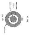
- FIG. 12is a top, cross-sectional view of a resonator with an output electrode with a circular shape and an input electrode which is spaced from and surrounds the output electrode in accordance with another embodiment
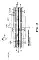
- FIG. 13is a side, cross-sectional view of the resonator shown in FIG. 11 with an input and an output;
- FIG. 14is side, cross-sectional view of a resonator with a member with embedded charge secured at substantially opposing ends in accordance with another embodiment of the present invention.
- FIG. 15is a side, cross-sectional view of a resonator in a transceiver with a member with embedded charge secured at one end in accordance with another embodiment of the present invention.
- FIG. 16is a perspective view of a portion of the resonator shown in FIG. 11;
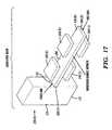
- FIG. 17is a perspective view of a portion of the resonator shown in FIG. 15;
- FIG. 18is a perspective view of a portion of a resonator in accordance with another embodiment of the present invention.
- FIG. 19is a perspective view of a portion of a resonator in accordance with another embodiment of the present invention with leads to an input, output, and tuning bias on the member;
- FIG. 20is a perspective view of a portion of a resonator in accordance with another embodiment of the present invention with leads to inputs, an output, and a common;
- FIG. 21is a perspective view of a portion of a resonator with a pair of input electrodes, an output electrode, and a common electrode in accordance with another embodiment of the present invention.
- FIG. 22is a side, cross-sectional view of the resonator with two pairs of corresponding input electrodes and a corresponding pair of output electrodes in accordance with another embodiment
- FIG. 23is a side, cross-sectional view of a resonator with corresponding input and output electrodes on each side of the member in accordance with another embodiment.
- FIG. 24is a side, cross-sectional view of a resonator with an input electrode, an output electrode, and a common electrode in accordance with another embodiment.
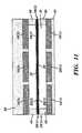
- FIGS. 1-11, 13 , and 16A method for making a resonator 10 ( 1 ) in accordance with an embodiment of the present invention is illustrated in FIGS. 1-11, 13 , and 16 .
- the resonator 10 ( 1 )includes a chamber 12 , a member or resonator membrane 14 ( 1 ) with an embedded charge 15 , two pairs of input electrodes 16 ( 1 )- 16 ( 2 ) and 18 ( 1 )- 18 ( 2 ) and one pair of output electrodes 20 ( 1 )- 20 ( 2 ), although the resonator can comprise other numbers and types of components.
- the present inventionprovides high Qrf-MEMS resonators 10 ( 1 )- 10 ( 5 ) which are not limited by stiction, can be made very small, can operate in a single mode, can operate at very high frequencies, and can be easily integrated with a variety of different types of semiconductor devices.
- FIGS. 11 and 13 - 24resonators 10 ( 1 )- 10 ( 9 ) in accordance with embodiments of the present invention are illustrated.
- Elements in FIGS. 12 and 14 - 24which are identical to those described with reference to FIGS. 1-11 and 13 , have like numerals. These like elements are identical except as described herein.
- each of the resonators 10 ( 1 )- 10 ( 9 )has a high Q, although other variations are possible.
- Qis defined as the center frequency divided by the bandwidth.
- the resonators 10 ( 1 )- 10 ( 9 )have a Q over about 1000, although the value of Q can vary.
- Each of the resonators 10 ( 1 )- 10 ( 9 )includes a chamber 12 which is made of a variety of layers, although other types of supporting structures for the member 14 ( 1 ), 14 ( 2 ), or 14 ( 3 ) and the electrodes 16 ( 1 ), 16 ( 2 ), 18 ( 1 ), 18 ( 2 ), 20 ( 1 ) and 20 ( 2 ) in other configurations and shapes and with other numbers of layers and made of other materials can be used.
- the size of the chamber 12can vary as required by the particular application. For ease of illustration, portions of the chamber 12 are not shown in FIGS. 16-21.
- Each of the resonators 10 ( 1 )- 10 ( 9 )also includes a member 14 ( 1 ), 14 ( 2 ) and 14 ( 3 ) with an embedded charge 15 .
- the member 14 ( 1 )comprises a pair of layers 22 ( 1 ) and 22 ( 2 ) of dielectric material, such as silicon oxide, silicon dioxide, silicon nitride, aluminum oxide, tantalum oxide, tantalum pentoxide, titanium oxide, titanium dioxide, barium strontium titanium oxide, or a material with residual polarization, such as an electret, although other types of materials could be used.
- the member 14 ( 2 )comprises a single layer 26 of dielectric material, such as such as silicon oxide, silicon dioxide, silicon nitride, aluminum oxide, tantalum oxide, tantalum pentoxide, titanium oxide, titanium dioxide, barium strontium titanium oxide, in which the embedded charge 15 is held.
- the embedded charge in the member 14 ( 3 )is a charged floating conductor.
- the member 14 ( 3 )comprises a single layer 27 of dielectric material, such as such as silicon oxide, silicon dioxide, silicon nitride, aluminum oxide, tantalum oxide, tantalum pentoxide, titanium oxide, titanium dioxide, barium strontium titanium oxide, with an embedded charge 15 that is a charged floating conductor.
- dielectric materialsuch as silicon oxide, silicon dioxide, silicon nitride, aluminum oxide, tantalum oxide, tantalum pentoxide, titanium oxide, titanium dioxide, barium strontium titanium oxide, with an embedded charge 15 that is a charged floating conductor.
- the member 14 ( 1 )is connected at one end 28 ( 1 ) to an inner wall of the chamber 12 , extends across the chamber 12 , and has another end 28 ( 2 ) which is connected on a substantially opposing side to another inner wall of the chamber 12 , although other configurations and other types of members can be used can be used.
- the chamber 12is not shown for ease of illustration, however the ends which are fixed are designated.
- the member 14 ( 1 )is secured on the layer of a layer of insulating material 38 and thus is fixed.
- the moving or resonating part of the resonators 10 ( 6 )- 10 ( 9 )are the electrodes 16 ( 2 ), 18 ( 2 ), and/or 20 ( 2 ) which are embedded in the insulating layer 50 , although other arrangements are possible, such as attaching the electrodes 16 ( 2 ), 18 ( 2 ), and/or 20 ( 2 ) to the insulating layer 50 or burying one or more of the electrodes 16 ( 2 ), 18 ( 2 ), and/or 20 ( 2 ) in the insulating layer 50 .
- the spacing of the member 14 ( 1 ) between the electrodes 16 ( 1 ), 17 , 18 ( 1 ), and/or 20 ( 1 ) and the member 14 ( 1 )is greater than the spacing between the electrodes 16 ( 2 ), 18 ( 2 ), and/or 20 ( 2 ) and the member 14 ( 1 ), the spacing is arranges so that the member 14 ( 1 ) is electrically centered in the resonators 10 ( 6 )- 10 ( 70 when the permitivities of the layer 38 and the permitivity of the air or other gas or fluid in the chamber 12 .
- the member 14 ( 2 )is connected at one end 30 ( 1 ) to an inner wall of the chamber 12 , extends across the chamber 12 , and has another end 30 ( 2 ) which is free and is spaced from another inner wall of the chamber 12 , although other configurations can be used and other types of members can be used.
- FIGS. 18-20other variations for connecting the member 14 ( 1 ), 14 ( 2 ), and 14 ( 3 ) are shown which enable the resonator to operate at a higher frequency range above about 100 MHz.
- the member 14 ( 1 )is connected along an elongated side 23 ( 1 ) to an inner wall of the chamber 12 and extends out into the chamber 12 and has another opposing elongated side 23 ( 2 ) that is free and is spaced from another inner wall of the chamber 12 and the ends 28 ( 1 ) and 28 ( 2 ) of the member 14 ( 1 ) are free, although other configurations can be used and other types of members can be used.
- FIGS. 18-20other variations for connecting the member 14 ( 1 ), 14 ( 2 ), and 14 ( 3 ) are shown which enable the resonator to operate at a higher frequency range above about 100 MHz.
- the member 14 ( 1 )is connected along an elongated side 23 ( 1 ) to an inner wall of the chamber 12 and extends out into the chamber 12 and has another
- the member 14 ( 3 )is also connected along an elongated side 27 ( 1 ) to an inner wall of the chamber 12 and extends out into the chamber 12 and has another opposing elongated side 27 ( 2 ) that is free and is spaced from another inner wall of the chamber 12 and the ends 31 ( 1 ) and 31 ( 2 ) of the member 14 ( 1 ) are free, although other configurations can be used and other types of members can be used.
- the resonators 10 ( 1 ), 10 ( 5 ), and 10 ( 7 )each include two pairs of input electrodes 16 ( 1 )- 16 ( 2 ) and 18 ( 1 )- 18 ( 2 ) and one pair of output electrodes 20 ( 1 )- 20 ( 2 ), although other combinations of pairs electrodes could be used, such as the resonators 10 ( 2 ), 10 ( 3 ), and 10 ( 8 ) with one pair of input electrodes 16 ( 1 )- 16 ( 2 ) and one pair of output electrodes 20 ( 1 )- 20 ( 2 ) as shown in FIGS.
- Each electrode 16 ( 2 ), 18 ( 2 ), and 20 ( 2 ) in each pairis spaced from and located on a substantially opposing sides of the member 14 ( 1 ) or member 14 ( 2 ) from the other electrode 16 ( 1 ), 18 ( 1 ), and 20 ( 1 ) in the pair or form the common electrode 17 .
- each of the pairs of electrodes 16 ( 1 )- 16 ( 2 ), 18 ( 1 )- 18 ( 2 ), and 20 ( 1 )- 20 ( 2 ) or 16 ( 2 ), 18 ( 2 ), and/or 20 ( 2 ) and common electrode 17is about 0.2 to 2.0 microns, although this distance can vary.
- Common electrode 17may be a direct connection to ground, although other configurations can be used, such as coupling to a common reference level.
- the two pairs of input electrodes 16 ( 1 )- 16 ( 2 ) and 18 ( 1 )- 18 ( 2 )are each adjacent opposing ends 28 ( 1 ) and 28 ( 2 ) or 31 ( 1 ) and 31 ( 2 ) of the member 14 ( 1 ) or 14 ( 3 ) and are located on opposing sides of the pair of output electrodes 20 ( 1 )- 20 ( 2 ), although other configurations could be used.
- the resonators 10 ( 1 ), 10 ( 5 ), and 10 ( 9 )could have one pair of output electrodes 20 ( 1 )- 20 ( 2 ) with a substantially circular shape surrounded by one pair of input electrodes 16 ( 1 )- 16 ( 2 ) having a substantially annulus shape as shown in FIG. 12, although the input and output electrodes could have other shapes or be in an opposite orientation.
- This one pair of input electrodes 16 ( 1 )- 16 ( 2 ) having an annulus shapewould replace the two pairs of input electrodes 16 ( 1 )- 16 ( 2 ) and 18 ( 1 )- 18 ( 2 ) shown in FIGS. 13, 16 , 19 , 20 , and 22 .
- one pair of input electrodes 16 ( 1 ) 16 ( 2 )are positioned adjacent one end 28 ( 1 ) of the member 14 ( 1 ) and the other pair of electrodes 20 ( 1 )- 20 ( 2 ) are adjacent the other end 28 ( 2 ) of the member 14 ( 1 ), although other configurations could be used.
- one pair of input electrodes 16 ( 1 )- 16 ( 2 )are positioned adjacent one end 28 ( 1 ) of the member 14 ( 2 ) and the other pair of electrodes 20 ( 1 )- 20 ( 2 ) are adjacent the other end 28 ( 2 ) of the member 14 ( 2 ), although other configurations could be used.
- input electrodes 16 ( 2 ) and 18 ( 2 )are each adjacent opposing ends 28 ( 1 ) and 28 ( 2 ) of the member 14 ( 1 ) and are located on opposing sides of the output electrodes 20 ( 2 ) and a common electrode 17 is on the opposing side of the member 14 ( 1 ) from electrodes 16 ( 2 ), 18 ( 2 ), and 20 ( 2 ), although other configurations could be used.
- input electrode 16 ( 2 ) and output electrode 20 ( 2 )are each adjacent opposing ends 28 ( 1 ) and 28 ( 2 ) of the member 14 ( 1 ) and a common electrode 17 is on the opposing side of the member 14 ( 1 ) from electrodes 16 ( 2 ) and 20 ( 2 ), although other configurations could be used.
- an input lead 52such as an antenna, is coupled to the input electrodes 16 ( 2 ) and 20 ( 2 ), although other types of input devices could be used.
- An output lead 54is coupled to the output electrode 20 ( 2 ), and a common, such as ground, is coupled to the input electrodes 16 ( 1 ) and 18 ( 1 ) and to output electrode 20 ( 1 ), although other common reference levels could be used.
- an input lead 52such as an antenna, is coupled to the input electrode 16 ( 2 ), although other types of input devices could be used.
- An output lead 54is coupled to the output electrode 20 ( 2 ), and a common, such as ground, is coupled to the input electrode 16 ( 1 ) and to output electrode 20 ( 1 ), although other common reference levels could be used.
- an input lead 52such as an antenna, is coupled to the input electrodes 16 ( 2 ) and 18 ( 2 ), although other types of input devices could be used.
- An output lead 54is coupled to the output electrode 20 ( 2 ), and a common, such as ground, is coupled to the common electrode 17 , although other common reference levels could be used.
- a tuning bias input 51 ( 1 ) and 51 ( 2 )is coupled to input electrodes 16 ( 1 ) and 16 ( 2 ) to tune the resonator 10 ( 5 ) to a particular frequency.
- the other resonators 10 ( 1 )- 10 ( 4 )can be configured to apply a tuning bias to tune the resonator to a particular frequency.
- An input lead 52 ( 1 ) and 52 ( 2 )is coupled across the input electrodes 18 ( 1 ) and 18 ( 2 ) and an output lead 54 ( 1 ) and 54 ( 2 ) is coupled across the output electrodes 20 ( 1 ) and 20 ( 2 ), although other configurations can be used.
- an input lead 52such as an antenna, is coupled to the input electrodes 16 ( 2 ) and 18 ( 2 ), although other types of input devices could be used.
- An output lead 54is coupled to the output electrode 20 ( 2 ), and a common, such as ground, is coupled to the common electrode 17 , although other common reference levels could be used.
- a method for making a resonator 10 ( 1 ) in accordance with an embodiment of the present invention in accordance with an embodimentwill be described with reference to FIGS. 1-11, 13 , and 16 .
- a layer 32 of insulating materialsuch as SiO 2 is provided, although other types of materials and other numbers of layers could be used.
- the layer 32 of insulating materialcould be deposited on a substrate which acts as the base.
- three openings or trenches 34 ( 1 )- 34 ( 3 )are patterned and etched into the layer 32 of insulating material and then a conductive material 36 , such as Cu, is deposited in each of the openings 34 ( 1 )- 34 ( 3 ) to form electrodes 16 ( 1 ), 18 ( 1 ), and 20 ( 1 ), although other types of conductive materials could be used, the number of openings etched can vary depending on the number of electrodes desired, and other techniques for forming the electrodes can be used.
- the deposited conductive material 36may be planarized.
- a layer 38 of insulating materialsuch as SiO 2 may be deposited on a portion of the conductive material 36 in the openings 34 ( 1 )- 34 ( 3 ) and on a portion of the exposed layer 32 of insulating material.
- an opening or trench 40is patterned and etched in the layer 38 of insulating material which extends to a portion of the conductive material 36 in the openings 34 ( 1 )- 34 ( 3 ) and on a portion of the exposed layer 32 of insulating material, although the opening 40 can extend to other depths, such as a depth where the electrodes 16 ( 1 ), 18 ( 1 ), and 20 ( 1 ) would still be covered by a portion of the layer 38 of insulating material or by another insulating layer or layers.
- a layer 42 of sacrificial materialsuch as polysilicon, is deposited in the opening 40 in the layer 38 of insulating material, although other types of sacrificial materials could be used, such as polymers.
- the layer 42 of sacrificial materialmay be planarized.
- a layer 22 ( 1 ) of insulating materialsuch as a layer of silicon oxide, is deposited on the layer 42 of sacrificial material and a portion of layer 38 of insulating material which is exposed.
- An embedded charge 15can be held at an interface 24 between the layers 22 ( 1 ) and 22 ( 2 ) of insulating material.
- the member 14 ( 1 )can be comprised of other numbers of layers, such as one layer 26 as shown in FIGS. 15 and 17, one layer 27 with embedded charge 15 which is a charged floating conductor as shown in FIGS. 19 and 20, or three or more layers.
- the embedded charge 15can be held at one or more of the interfaces between the multiple layers.
- electronsare injected into the member 14 ( 1 ) with an electron gun to deposit an embedded charge 15
- other techniques for storing embedded charge 15 in the member 14 ( 1 )can also be used, such as applying an electrical bias across the member 14 ( 1 ) sufficient to cause electron injection, ballistic injection, polarization, and high field injection.
- the same techniquescan be used to store an embedded charge 15 in the member 14 ( 2 ) shown in FIGS. 15 and 17 and a charged floating conductor as the embedded charge 15 in the member 14 ( 3 ) in FIGS. 19 and 20.
- a layer 44 of insulating materialsuch as SiO 2 , is deposited on the member 14 ( 1 ), although other types of insulating materials could be used.
- an opening or trench 46is patterned and etched in the layer 44 of insulating material which extends to member 14 ( 1 ).
- a layer 48 of sacrificial materialsuch as polysilicon, is deposited in the opening 46 in the layer 44 of insulating material, although other types of sacrificial materials could be used.
- the layer 48 of sacrificial materialmay be planarized.
- a layer 49 of conductive materialsuch as Cu, is deposited on the layer 48 of sacrificial material and on the exposed portion of the layer 44 of insulating material, although other types of conductive materials could be used.
- the layer 49 of conductive materialis patterned and etched to form electrodes 16 ( 2 ), 18 ( 2 ), and 20 ( 2 ).
- a layer 50 of insulating materialsuch as SiO 2 is deposited over the remaining portion of the layer of conductive material 49 which forms electrodes 16 ( 2 ), 18 ( 2 ), and 20 ( 2 ).
- the layer 50 of insulating materialencapsulates and supports the electrodes 16 ( 2 ), 18 ( 2 ), and 20 ( 2 ).
- an access hole or holes(not shown) to the layers 42 and 48 of sacrificial material are formed and the layers 42 and 48 of sacrificial material are removed through the access hole or holes to form the chamber 12 , although other techniques for removing the layers 42 and 48 of sacrificial material can be used.
- the access hole or holesare closed and the chamber 12 can be sealed in a vacuum or filled with one or more gases depending on the particular application.
- electrodes 16 ( 1 ), 16 ( 2 ), 17 , 18 ( 1 ), 18 ( 2 ), 20 ( 1 ), and 20 ( 2 )for the different resonators 10 ( 1 )- 10 ( 5 ) for providing access for electrical contact, although other techniques for providing electrical coupling to electrodes 16 ( 1 ), 16 ( 2 ), 17 18 ( 1 ), 18 ( 2 ), 20 ( 1 ), and 20 ( 2 ) could be used.
- the method for making the resonator 10 ( 2 ) shown in FIG. 14is the same as the method described above for making the resonator 10 ( 1 ) shown in FIGS. 11, 13 , and 16 except as described below.
- the layer 32 of insulating material shown in FIG. 2is patterned and etched to form two openings which are filled with the conductive material 36 to form the two electrodes 16 ( 1 ) and 20 ( 1 ).
- the layer 49 of conducting material shown in FIG. 9is patterned and etched to form the two electrodes 16 ( 2 ) and 20 ( 2 ).
- the method for making the resonator 10 ( 3 ) shown in FIGS. 15 and 17is the same as the method described above for making the resonator 10 ( 1 ) shown in FIGS. 11, 13 , and 16 except as described below.
- the layer 32 of insulating material shown in FIG. 2is patterned and etched to form two openings which are filled with the conductive material 36 to form the two electrodes 16 ( 1 ) and 20 ( 1 ).
- the layer 49 of conducting material shown in FIG. 9is patterned and etched to form the two electrodes 16 ( 2 ) and 20 ( 2 ).
- the method for making the resonator 10 ( 4 ) shown in FIG. 18is the same as the method described above for making the resonator 10 ( 1 ) shown in FIGS. 11, 13 , and 16 except as described below.
- the layer 32 of insulating material shown in FIG. 2is not patterned and etched.
- the deposited layer of conductive material 36is not patterned or etched and forms the common electrode 17 , although other arrangements can be used, such as starting with a substrate made of a conductive material which acts as the common electrode 17 .
- the method for making the resonator 10 ( 5 ) shown in FIGS. 19 and 20is the same as the method described above for making the resonator 10 ( 1 ) shown in FIGS. 11, 13 , and 16 except as described below.
- the layers of insulating material 22 ( 1 ) and 22 ( 2 ) which comprise member 14 ( 1 )are formed to have ends 28 ( 1 ) and 28 ( 2 ) free and spaced from the inner wall of the chamber 12 , elongated side 23 ( 1 ) of the member 14 ( 1 ) is secured in the inner wall of the chamber 12 , and elongated side 23 ( 2 ) is free and spaced form the inner wall of the chamber 12 , although other configurations could be used.
- the method for making the resonator 10 ( 6 ) shown in FIG. 21is the same as the method described above for making the resonator 10 ( 1 ) shown in FIGS. 11, 13 , and 16 except as described below.
- the deposited layer of conductive material 36is not patterned or etched and forms the common electrode 17 , although other arrangements can be used, such as starting with a substrate made of a conductive material which acts as the common electrode 17 .
- the layer 38 of insulating material shown in FIG. 3is not patterned or etched and the layer 22 ( 1 ) of the member 14 ( 1 ) is formed on the layer 38 .
- Electrode 10is formed to have ends 59 ( 1 ) and 59 ( 2 ) and elongated side 61 ( 1 ) free, while elongated side 61 ( 2 ) of layer 50 is fixed so that the electrodes 16 ( 2 ), 18 ( 2 ), and 20 ( 2 ) and layer 50 can move and resonate.
- the method for making the resonator 10 ( 7 ) shown in FIG. 22is the same as the method described above for making the resonator 10 ( 1 ) shown in FIGS. 11, 13 , and 16 except as described below.
- the layer 38 of insulating material shown in FIG. 3is not patterned or etched and the layer 22 ( 1 ) of the member 14 ( 1 ) is formed on the layer 38 .
- the layer 50 of insulating material shown in FIG. 10is formed so that the electrodes 16 ( 2 ), 18 ( 2 ), and 20 ( 2 ) and layer 50 can move and resonate.
- the method for making the resonator 10 ( 8 ) shown in FIG. 23is the same as the method described above for making the resonator 10 ( 1 ) shown in FIGS. 11, 13 , and 16 except as described below.
- the layer 32 of insulating material shown in FIG. 2is patterned and etched to form two openings which are filled with the conductive material 36 to form the two electrodes 16 ( 1 ) and 20 ( 1 ).
- the layer 38 of insulating material shown in FIG. 3is not patterned or etched and the layer 22 ( 1 ) of the member 14 ( 1 ) is formed on the layer 38 .
- the layer 50 of insulating material shown in FIG. 10is formed so that the electrodes 16 ( 2 ) and 20 ( 2 ) and layer 50 can move and resonate.
- the method for making the resonator 10 ( 9 ) shown in FIG. 24is the same as the method described above for making the resonator 10 ( 1 ) shown in FIGS. 11, 13 , and 16 except as described below.
- a substrate made of a layer 17 of conductive materialis provided that is not patterned or etched and forms the common electrode 17 , although other arrangements can be used, such as using other numbers and types of layers of materials.
- the layer 38 of insulating material shown in FIG. 3is not patterned or etched and the layer 22 ( 1 ) of the member 14 ( 1 ) is formed on the layer 38 .
- the layer 50 of insulating material shown in FIG. 10is formed so that the electrodes 16 ( 2 ) and 20 ( 2 ) and layer 50 can move and resonate.
- the operation of the resonators 10 ( 1 )- 10 ( 9 ) to pass one or more signalswill now be discussed with reference to FIGS. 13-24. If a tuning bias is applied across the tuning bias inputs 51 ( 2 ) and 51 ( 2 ), the resonant frequency of the resonator can be tuned to a particular frequency.
- the incoming signalapplies or induces a varying signal, such as a varying amplitude signal or a varying frequency signal, on the pairs of input electrodes 16 ( 1 ), 16 ( 2 ), 18 ( 1 ), and/or 18 ( 2 ) coupled to the input lead 52 or across the leads 52 ( 1 ) and 52 ( 2 ) which correlates to the resonant portion of the incoming signal.
- a varying signalsuch as a varying amplitude signal or a varying frequency signal
- the varying signal on the pairs of input electrodes 16 ( 1 )- 16 ( 2 ) and 18 ( 1 )- 18 ( 2 ) or 16 ( 1 )- 16 ( 2 )causes the member 14 ( 1 ) or 14 ( 2 ) with the embedded charge 15 to oscillate in response to the received varying signal.
- the movement of the member 14 ( 1 ) or 14 ( 2 ) with the embedded charge 15causes a varying signal, such as a varying amplitude signal or a varying frequency signal, to be applied or induced on the pairs of output electrodes 20 ( 1 )- 20 ( 2 ) which is transmitted out as an output signal on the output lead 54 or across the output leads 54 ( 1 ) and 54 ( 2 ).
- the outgoing signalWhen the output lead 54 or leads 54 ( 1 ) and 54 ( 2 ) receives an outgoing signal at the resonant frequency to transmit, the outgoing signal induces a varying signal, such as a varying amplitude signal or a varying frequency signal, on the pairs of output electrodes 20 ( 1 )- 20 ( 2 ) in response to the outgoing signal.
- the varying signal on the pairs of output electrodes 20 ( 1 )- 20 ( 2 )causes the member 14 ( 1 ) or 14 ( 2 ) with the embedded charge 15 to oscillate in response to the varying signal.
- the movement of the member 14 ( 1 ) or 14 ( 2 ) with the embedded charge 15causes a varying signal, such as a varying amplitude signal or a varying frequency signal, to be applied or induced on the pairs of input electrodes 16 ( 1 ) 16 ( 2 ) and 18 ( 1 )- 18 ( 2 ) or 16 ( 1 )- 16 ( 2 ) which is transmitted out as an outgoing signal via the input leads 52 or across the input leads 52 ( 1 ) and 52 ( 2 ).
- these resonators 10 ( 1 )- 10 ( 9 )can be used to eliminate the need for some components, such as separate transmit/receive cell phone boards.
- an embedded charge density of 1e12 charges per cm 2 on the member and an oscillation sufficient to change the induced charge on an output set of electrodes by 1%will cause a voltage swing of 0.36 V.
- an average oscillation displacement of only a few tens of angstromsyields a significant output signal.
Landscapes
- Physics & Mathematics (AREA)
- Acoustics & Sound (AREA)
- Engineering & Computer Science (AREA)
- Manufacturing & Machinery (AREA)
- Micromachines (AREA)
Abstract
Description
Claims (56)
Priority Applications (2)
| Application Number | Priority Date | Filing Date | Title |
|---|---|---|---|
| US10/238,438US6717488B2 (en) | 2001-09-13 | 2002-09-09 | Resonator with a member having an embedded charge and a method of making thereof |
| US10/453,247US6842009B2 (en) | 2001-09-13 | 2003-06-03 | Biohazard sensing system and methods thereof |
Applications Claiming Priority (2)
| Application Number | Priority Date | Filing Date | Title |
|---|---|---|---|
| US31891401P | 2001-09-13 | 2001-09-13 | |
| US10/238,438US6717488B2 (en) | 2001-09-13 | 2002-09-09 | Resonator with a member having an embedded charge and a method of making thereof |
Related Child Applications (1)
| Application Number | Title | Priority Date | Filing Date |
|---|---|---|---|
| US10/453,247Continuation-In-PartUS6842009B2 (en) | 2001-09-13 | 2003-06-03 | Biohazard sensing system and methods thereof |
Publications (2)
| Publication Number | Publication Date |
|---|---|
| US20030112096A1 US20030112096A1 (en) | 2003-06-19 |
| US6717488B2true US6717488B2 (en) | 2004-04-06 |
Family
ID=23240098
Family Applications (1)
| Application Number | Title | Priority Date | Filing Date |
|---|---|---|---|
| US10/238,438Expired - Fee RelatedUS6717488B2 (en) | 2001-09-13 | 2002-09-09 | Resonator with a member having an embedded charge and a method of making thereof |
Country Status (2)
| Country | Link |
|---|---|
| US (1) | US6717488B2 (en) |
| WO (1) | WO2003023957A1 (en) |
Cited By (17)
| Publication number | Priority date | Publication date | Assignee | Title |
|---|---|---|---|---|
| US20020131228A1 (en)* | 2001-03-13 | 2002-09-19 | Potter Michael D. | Micro-electro-mechanical switch and a method of using and making thereof |
| US20020182091A1 (en)* | 2001-05-31 | 2002-12-05 | Potter Michael D. | Micro fluidic valves, agitators, and pumps and methods thereof |
| US20040023236A1 (en)* | 2001-10-26 | 2004-02-05 | Potter Michael D. | Chemical and biological hazard sensor system and methods thereof |
| US20040145271A1 (en)* | 2001-10-26 | 2004-07-29 | Potter Michael D | Electrostatic based power source and methods thereof |
| US20040155555A1 (en)* | 2001-10-26 | 2004-08-12 | Potter Michael D. | Electrostatic based power source and methods thereof |
| US20050044955A1 (en)* | 2003-08-29 | 2005-03-03 | Potter Michael D. | Methods for distributed electrode injection and systems thereof |
| US20050205966A1 (en)* | 2004-02-19 | 2005-09-22 | Potter Michael D | High Temperature embedded charge devices and methods thereof |
| US20050207100A1 (en)* | 2004-03-17 | 2005-09-22 | Heckerman Donald A | Flat screen display stand |
| US20070074731A1 (en)* | 2005-10-05 | 2007-04-05 | Nth Tech Corporation | Bio-implantable energy harvester systems and methods thereof |
| US7217582B2 (en) | 2003-08-29 | 2007-05-15 | Rochester Institute Of Technology | Method for non-damaging charge injection and a system thereof |
| US20080054759A1 (en)* | 2006-08-11 | 2008-03-06 | Farrokh Ayazi | Wafer-level encapsulation and sealing of electrostatic transducers |
| US20090057792A1 (en)* | 2004-12-22 | 2009-03-05 | Koninklijke Philips Electronics N.V. | Charge biased mem resonator |
| US7544531B1 (en) | 2007-03-13 | 2009-06-09 | Sitime Inc. | Ground strap for suppressing stiction during MEMS fabrication |
| US7757393B2 (en) | 2005-06-03 | 2010-07-20 | Georgia Tech Research Corporation | Capacitive microaccelerometers and fabrication methods |
| US7767484B2 (en) | 2006-05-31 | 2010-08-03 | Georgia Tech Research Corporation | Method for sealing and backside releasing of microelectromechanical systems |
| US20120105173A1 (en)* | 2009-05-29 | 2012-05-03 | Infineon Technologies Ag | MEMS Device |
| US8372677B2 (en) | 2006-05-10 | 2013-02-12 | Qualtre, Inc. | Three-axis accelerometers and fabrication methods |
Families Citing this family (54)
| Publication number | Priority date | Publication date | Assignee | Title |
|---|---|---|---|---|
| US7550794B2 (en) | 2002-09-20 | 2009-06-23 | Idc, Llc | Micromechanical systems device comprising a displaceable electrode and a charge-trapping layer |
| US7297471B1 (en) | 2003-04-15 | 2007-11-20 | Idc, Llc | Method for manufacturing an array of interferometric modulators |
| US6794119B2 (en) | 2002-02-12 | 2004-09-21 | Iridigm Display Corporation | Method for fabricating a structure for a microelectromechanical systems (MEMS) device |
| EP1512216A2 (en)* | 2002-06-07 | 2005-03-09 | California Institute Of Technology | Electret generator apparatus and method |
| AU2003238881A1 (en)* | 2002-06-07 | 2003-12-22 | California Institute Of Technology | Method and resulting device for fabricating electret materials on bulk substrates |
| US7781850B2 (en) | 2002-09-20 | 2010-08-24 | Qualcomm Mems Technologies, Inc. | Controlling electromechanical behavior of structures within a microelectromechanical systems device |
| TW594360B (en) | 2003-04-21 | 2004-06-21 | Prime View Int Corp Ltd | A method for fabricating an interference display cell |
| TW570896B (en)* | 2003-05-26 | 2004-01-11 | Prime View Int Co Ltd | A method for fabricating an interference display cell |
| US7221495B2 (en)* | 2003-06-24 | 2007-05-22 | Idc Llc | Thin film precursor stack for MEMS manufacturing |
| TWI231865B (en) | 2003-08-26 | 2005-05-01 | Prime View Int Co Ltd | An interference display cell and fabrication method thereof |
| TW593126B (en) | 2003-09-30 | 2004-06-21 | Prime View Int Co Ltd | A structure of a micro electro mechanical system and manufacturing the same |
| US7405861B2 (en) | 2004-09-27 | 2008-07-29 | Idc, Llc | Method and device for protecting interferometric modulators from electrostatic discharge |
| US7369296B2 (en) | 2004-09-27 | 2008-05-06 | Idc, Llc | Device and method for modifying actuation voltage thresholds of a deformable membrane in an interferometric modulator |
| US7553684B2 (en) | 2004-09-27 | 2009-06-30 | Idc, Llc | Method of fabricating interferometric devices using lift-off processing techniques |
| US7417783B2 (en) | 2004-09-27 | 2008-08-26 | Idc, Llc | Mirror and mirror layer for optical modulator and method |
| US7684104B2 (en) | 2004-09-27 | 2010-03-23 | Idc, Llc | MEMS using filler material and method |
| US7349136B2 (en) | 2004-09-27 | 2008-03-25 | Idc, Llc | Method and device for a display having transparent components integrated therein |
| US7492502B2 (en) | 2004-09-27 | 2009-02-17 | Idc, Llc | Method of fabricating a free-standing microstructure |
| US7161730B2 (en)* | 2004-09-27 | 2007-01-09 | Idc, Llc | System and method for providing thermal compensation for an interferometric modulator display |
| US7373026B2 (en) | 2004-09-27 | 2008-05-13 | Idc, Llc | MEMS device fabricated on a pre-patterned substrate |
| US7429334B2 (en) | 2004-09-27 | 2008-09-30 | Idc, Llc | Methods of fabricating interferometric modulators by selectively removing a material |
| TW200628877A (en) | 2005-02-04 | 2006-08-16 | Prime View Int Co Ltd | Method of manufacturing optical interference type color display |
| KR101375337B1 (en) | 2005-07-22 | 2014-03-18 | 퀄컴 엠이엠에스 테크놀로지스, 인크. | Electomechanical devices having support structures and methods of fabricating the same |
| KR20080041663A (en) | 2005-07-22 | 2008-05-13 | 콸콤 인코포레이티드 | Supporting structures for MEMS devices and methods thereof |
| EP2495212A3 (en) | 2005-07-22 | 2012-10-31 | QUALCOMM MEMS Technologies, Inc. | Mems devices having support structures and methods of fabricating the same |
| US7630114B2 (en) | 2005-10-28 | 2009-12-08 | Idc, Llc | Diffusion barrier layer for MEMS devices |
| US7795061B2 (en) | 2005-12-29 | 2010-09-14 | Qualcomm Mems Technologies, Inc. | Method of creating MEMS device cavities by a non-etching process |
| US7382515B2 (en) | 2006-01-18 | 2008-06-03 | Qualcomm Mems Technologies, Inc. | Silicon-rich silicon nitrides as etch stops in MEMS manufacture |
| US7547568B2 (en) | 2006-02-22 | 2009-06-16 | Qualcomm Mems Technologies, Inc. | Electrical conditioning of MEMS device and insulating layer thereof |
| US7450295B2 (en) | 2006-03-02 | 2008-11-11 | Qualcomm Mems Technologies, Inc. | Methods for producing MEMS with protective coatings using multi-component sacrificial layers |
| US20070228156A1 (en)* | 2006-03-28 | 2007-10-04 | Household Corporation | Interoperability facilitator |
| US7643203B2 (en)* | 2006-04-10 | 2010-01-05 | Qualcomm Mems Technologies, Inc. | Interferometric optical display system with broadband characteristics |
| US7417784B2 (en)* | 2006-04-19 | 2008-08-26 | Qualcomm Mems Technologies, Inc. | Microelectromechanical device and method utilizing a porous surface |
| US7527996B2 (en) | 2006-04-19 | 2009-05-05 | Qualcomm Mems Technologies, Inc. | Non-planar surface structures and process for microelectromechanical systems |
| US7623287B2 (en) | 2006-04-19 | 2009-11-24 | Qualcomm Mems Technologies, Inc. | Non-planar surface structures and process for microelectromechanical systems |
| US7711239B2 (en)* | 2006-04-19 | 2010-05-04 | Qualcomm Mems Technologies, Inc. | Microelectromechanical device and method utilizing nanoparticles |
| US7369292B2 (en) | 2006-05-03 | 2008-05-06 | Qualcomm Mems Technologies, Inc. | Electrode and interconnect materials for MEMS devices |
| US7405863B2 (en) | 2006-06-01 | 2008-07-29 | Qualcomm Mems Technologies, Inc. | Patterning of mechanical layer in MEMS to reduce stresses at supports |
| US7321457B2 (en)* | 2006-06-01 | 2008-01-22 | Qualcomm Incorporated | Process and structure for fabrication of MEMS device having isolated edge posts |
| US7763546B2 (en) | 2006-08-02 | 2010-07-27 | Qualcomm Mems Technologies, Inc. | Methods for reducing surface charges during the manufacture of microelectromechanical systems devices |
| US7566664B2 (en) | 2006-08-02 | 2009-07-28 | Qualcomm Mems Technologies, Inc. | Selective etching of MEMS using gaseous halides and reactive co-etchants |
| US7545552B2 (en) | 2006-10-19 | 2009-06-09 | Qualcomm Mems Technologies, Inc. | Sacrificial spacer process and resultant structure for MEMS support structure |
| US7706042B2 (en) | 2006-12-20 | 2010-04-27 | Qualcomm Mems Technologies, Inc. | MEMS device and interconnects for same |
| US7535621B2 (en) | 2006-12-27 | 2009-05-19 | Qualcomm Mems Technologies, Inc. | Aluminum fluoride films for microelectromechanical system applications |
| US7719752B2 (en) | 2007-05-11 | 2010-05-18 | Qualcomm Mems Technologies, Inc. | MEMS structures, methods of fabricating MEMS components on separate substrates and assembly of same |
| US7625825B2 (en)* | 2007-06-14 | 2009-12-01 | Qualcomm Mems Technologies, Inc. | Method of patterning mechanical layer for MEMS structures |
| US8068268B2 (en) | 2007-07-03 | 2011-11-29 | Qualcomm Mems Technologies, Inc. | MEMS devices having improved uniformity and methods for making them |
| US7851875B2 (en) | 2008-01-11 | 2010-12-14 | Infineon Technologies Ag | MEMS devices and methods of manufacture thereof |
| US7863079B2 (en) | 2008-02-05 | 2011-01-04 | Qualcomm Mems Technologies, Inc. | Methods of reducing CD loss in a microelectromechanical device |
| US8125046B2 (en) | 2008-06-04 | 2012-02-28 | Infineon Technologies Ag | Micro-electromechanical system devices |
| US8299874B2 (en)* | 2008-07-25 | 2012-10-30 | The Invention Science Fund I, Llc | Rolled resonant element |
| US8659816B2 (en) | 2011-04-25 | 2014-02-25 | Qualcomm Mems Technologies, Inc. | Mechanical layer and methods of making the same |
| CN105210293A (en)* | 2013-03-11 | 2015-12-30 | 诺基亚技术有限公司 | Apparatus and method for tuning a resonance frequency |
| KR20170069806A (en)* | 2015-12-11 | 2017-06-21 | 현대자동차주식회사 | Manufacturing method of micro electro mechanical system sensor |
Citations (11)
| Publication number | Priority date | Publication date | Assignee | Title |
|---|---|---|---|---|
| US3715500A (en) | 1971-07-21 | 1973-02-06 | Bell Telephone Labor Inc | Unidirectional microphones |
| US5491604A (en) | 1992-12-11 | 1996-02-13 | The Regents Of The University Of California | Q-controlled microresonators and tunable electronic filters using such resonators |
| US5640133A (en) | 1995-06-23 | 1997-06-17 | Cornell Research Foundation, Inc. | Capacitance based tunable micromechanical resonators |
| US5668303A (en) | 1992-04-30 | 1997-09-16 | Forschung E.V Fraunhofer-Gesellschaft Zur Foerderung Der Angewandten | Sensor having a membrane as part of an electromechanical resonance circuit forming receiver and transmitter converter with interdigital structures spaced apart from one another |
| US5839062A (en) | 1994-03-18 | 1998-11-17 | The Regents Of The University Of California | Mixing, modulation and demodulation via electromechanical resonators |
| US5914553A (en) | 1997-06-16 | 1999-06-22 | Cornell Research Foundation, Inc. | Multistable tunable micromechanical resonators |
| US5919364A (en) | 1996-06-24 | 1999-07-06 | Regents Of The University Of California | Microfabricated filter and shell constructed with a permeable membrane |
| US5994982A (en) | 1997-07-18 | 1999-11-30 | Trw Inc. | MEMS switched resonators for VCO applications |
| US6204737B1 (en) | 1998-06-02 | 2001-03-20 | Nokia Mobile Phones, Ltd | Piezoelectric resonator structures with a bending element performing a voltage controlled switching function |
| US6238946B1 (en) | 1999-08-17 | 2001-05-29 | International Business Machines Corporation | Process for fabricating single crystal resonant devices that are compatible with integrated circuit processing |
| US6275122B1 (en) | 1999-08-17 | 2001-08-14 | International Business Machines Corporation | Encapsulated MEMS band-pass filter for integrated circuits |
- 2002
- 2002-09-09USUS10/238,438patent/US6717488B2/ennot_activeExpired - Fee Related
- 2002-09-10WOPCT/US2002/028894patent/WO2003023957A1/ennot_activeApplication Discontinuation
Patent Citations (12)
| Publication number | Priority date | Publication date | Assignee | Title |
|---|---|---|---|---|
| US3715500A (en) | 1971-07-21 | 1973-02-06 | Bell Telephone Labor Inc | Unidirectional microphones |
| US5668303A (en) | 1992-04-30 | 1997-09-16 | Forschung E.V Fraunhofer-Gesellschaft Zur Foerderung Der Angewandten | Sensor having a membrane as part of an electromechanical resonance circuit forming receiver and transmitter converter with interdigital structures spaced apart from one another |
| US5491604A (en) | 1992-12-11 | 1996-02-13 | The Regents Of The University Of California | Q-controlled microresonators and tunable electronic filters using such resonators |
| US5955932A (en) | 1992-12-11 | 1999-09-21 | The Regents Of The University Of California | Q-controlled microresonators and tunable electric filters using such resonators |
| US5839062A (en) | 1994-03-18 | 1998-11-17 | The Regents Of The University Of California | Mixing, modulation and demodulation via electromechanical resonators |
| US5640133A (en) | 1995-06-23 | 1997-06-17 | Cornell Research Foundation, Inc. | Capacitance based tunable micromechanical resonators |
| US5919364A (en) | 1996-06-24 | 1999-07-06 | Regents Of The University Of California | Microfabricated filter and shell constructed with a permeable membrane |
| US5914553A (en) | 1997-06-16 | 1999-06-22 | Cornell Research Foundation, Inc. | Multistable tunable micromechanical resonators |
| US5994982A (en) | 1997-07-18 | 1999-11-30 | Trw Inc. | MEMS switched resonators for VCO applications |
| US6204737B1 (en) | 1998-06-02 | 2001-03-20 | Nokia Mobile Phones, Ltd | Piezoelectric resonator structures with a bending element performing a voltage controlled switching function |
| US6238946B1 (en) | 1999-08-17 | 2001-05-29 | International Business Machines Corporation | Process for fabricating single crystal resonant devices that are compatible with integrated circuit processing |
| US6275122B1 (en) | 1999-08-17 | 2001-08-14 | International Business Machines Corporation | Encapsulated MEMS band-pass filter for integrated circuits |
Non-Patent Citations (1)
| Title |
|---|
| S. Cass, "Large Jobs For Little Devices," IEEE Spectrum, pp. 72-73 (2001). |
Cited By (27)
| Publication number | Priority date | Publication date | Assignee | Title |
|---|---|---|---|---|
| US20020131228A1 (en)* | 2001-03-13 | 2002-09-19 | Potter Michael D. | Micro-electro-mechanical switch and a method of using and making thereof |
| US7280014B2 (en) | 2001-03-13 | 2007-10-09 | Rochester Institute Of Technology | Micro-electro-mechanical switch and a method of using and making thereof |
| US20020182091A1 (en)* | 2001-05-31 | 2002-12-05 | Potter Michael D. | Micro fluidic valves, agitators, and pumps and methods thereof |
| US7195393B2 (en) | 2001-05-31 | 2007-03-27 | Rochester Institute Of Technology | Micro fluidic valves, agitators, and pumps and methods thereof |
| US20040145271A1 (en)* | 2001-10-26 | 2004-07-29 | Potter Michael D | Electrostatic based power source and methods thereof |
| US20040155555A1 (en)* | 2001-10-26 | 2004-08-12 | Potter Michael D. | Electrostatic based power source and methods thereof |
| US7378775B2 (en) | 2001-10-26 | 2008-05-27 | Nth Tech Corporation | Motion based, electrostatic power source and methods thereof |
| US7211923B2 (en) | 2001-10-26 | 2007-05-01 | Nth Tech Corporation | Rotational motion based, electrostatic power source and methods thereof |
| US20040023236A1 (en)* | 2001-10-26 | 2004-02-05 | Potter Michael D. | Chemical and biological hazard sensor system and methods thereof |
| US20050044955A1 (en)* | 2003-08-29 | 2005-03-03 | Potter Michael D. | Methods for distributed electrode injection and systems thereof |
| US7408236B2 (en) | 2003-08-29 | 2008-08-05 | Nth Tech | Method for non-damaging charge injection and system thereof |
| US7287328B2 (en) | 2003-08-29 | 2007-10-30 | Rochester Institute Of Technology | Methods for distributed electrode injection |
| US7217582B2 (en) | 2003-08-29 | 2007-05-15 | Rochester Institute Of Technology | Method for non-damaging charge injection and a system thereof |
| US20070152776A1 (en)* | 2003-08-29 | 2007-07-05 | Nth Tech Corporation | Method for non-damaging charge injection and system thereof |
| US20050205966A1 (en)* | 2004-02-19 | 2005-09-22 | Potter Michael D | High Temperature embedded charge devices and methods thereof |
| US8581308B2 (en) | 2004-02-19 | 2013-11-12 | Rochester Institute Of Technology | High temperature embedded charge devices and methods thereof |
| US20050207100A1 (en)* | 2004-03-17 | 2005-09-22 | Heckerman Donald A | Flat screen display stand |
| US20090057792A1 (en)* | 2004-12-22 | 2009-03-05 | Koninklijke Philips Electronics N.V. | Charge biased mem resonator |
| US8183946B2 (en) | 2004-12-22 | 2012-05-22 | Nxp B.V. | Charge biased MEM resonator |
| US7757393B2 (en) | 2005-06-03 | 2010-07-20 | Georgia Tech Research Corporation | Capacitive microaccelerometers and fabrication methods |
| US20070074731A1 (en)* | 2005-10-05 | 2007-04-05 | Nth Tech Corporation | Bio-implantable energy harvester systems and methods thereof |
| US8372677B2 (en) | 2006-05-10 | 2013-02-12 | Qualtre, Inc. | Three-axis accelerometers and fabrication methods |
| US7767484B2 (en) | 2006-05-31 | 2010-08-03 | Georgia Tech Research Corporation | Method for sealing and backside releasing of microelectromechanical systems |
| US20080054759A1 (en)* | 2006-08-11 | 2008-03-06 | Farrokh Ayazi | Wafer-level encapsulation and sealing of electrostatic transducers |
| US7544531B1 (en) | 2007-03-13 | 2009-06-09 | Sitime Inc. | Ground strap for suppressing stiction during MEMS fabrication |
| US20120105173A1 (en)* | 2009-05-29 | 2012-05-03 | Infineon Technologies Ag | MEMS Device |
| US9083308B2 (en)* | 2009-05-29 | 2015-07-14 | Infineon Technologies Ag | MEMS device |
Also Published As
| Publication number | Publication date |
|---|---|
| WO2003023957A1 (en) | 2003-03-20 |
| US20030112096A1 (en) | 2003-06-19 |
Similar Documents
| Publication | Publication Date | Title |
|---|---|---|
| US6717488B2 (en) | Resonator with a member having an embedded charge and a method of making thereof | |
| US7135940B2 (en) | Tunable filter and portable telephone | |
| KR100506729B1 (en) | Film bulk acoustic resonator and method for fabrication thereof | |
| EP1482638B1 (en) | Film bulk acoustic resonator having supports and manufacturing method therefor | |
| US6870445B2 (en) | Thin film bulk acoustic wave resonator | |
| KR100729795B1 (en) | Apparatus comprising a micromechanical resonator having an operating frequency and a method of extending the same | |
| US7986075B2 (en) | Film bulk acoustic wave resonator, its fabrication method and film bulk acoustic wave resonator filter using the resonator | |
| US7233218B2 (en) | Air-gap type FBAR, and duplexer using the FBAR | |
| FI108583B (en) | resonator structures | |
| KR102117471B1 (en) | Acoustic resonator and manufacturing method thereof | |
| US7301260B2 (en) | Bulk acoustic wave device and method of manufacturing the same | |
| JP3823032B2 (en) | Communication signal mixing / filtering device and manufacturing method thereof | |
| CN101931379B (en) | Resonator and a method of manufacturing the same, and oscillator and electronic apparatus including the same | |
| US20100295138A1 (en) | Methods and systems for fabrication of mems cmos devices | |
| US7002787B2 (en) | Capacitor apparatus of the capacity variable type | |
| US20160163954A1 (en) | Acoustic resonator and method of manufacturing the same | |
| EP1548939B1 (en) | Duplexer and method of fabrication | |
| KR20120023285A (en) | Bulk acoustic wave resonator structure and manufacturing method thereof | |
| US7382078B2 (en) | Electrostatic discharge protection of thin-film resonators | |
| CN111092604B (en) | Cavity structure of bulk acoustic wave resonator and manufacturing method | |
| EP1177622B1 (en) | Electronic device | |
| US7453332B2 (en) | Mechanical resonator | |
| KR100488615B1 (en) | Piezoelectric resonator, manufacturing method for the same, piezoelectric filter, manufacturing method for the same, duplexer, and electronic communication device | |
| KR101760029B1 (en) | Bulk acoustic wave resonator structure and manufacturing method thereof | |
| CN117579026B (en) | Film bulk acoustic resonator and preparation method thereof |
Legal Events
| Date | Code | Title | Description |
|---|---|---|---|
| AS | Assignment | Owner name:ROCHESTER INSTITUTE OF TECHNOLGY, NEW YORK Free format text:ASSIGNMENT OF ASSIGNORS INTEREST;ASSIGNOR:POTTER, MICHAEL D.;REEL/FRAME:013732/0981 Effective date:20030109 Owner name:ROCHESTER INSTITUTE OF TECHNOLOGY, NEW YORK Free format text:ASSIGNMENT OF ASSIGNORS INTEREST;ASSIGNOR:POTTER, MICHAEL D.;REEL/FRAME:013731/0019 Effective date:20030113 | |
| AS | Assignment | Owner name:NTH TECH CORPORATION, NEW YORK Free format text:ASSIGNMENT OF ASSIGNORS INTEREST;ASSIGNOR:POTTER, MICHAEL D.;REEL/FRAME:013860/0662 Effective date:20030312 | |
| AS | Assignment | Owner name:NTH TECH CORPORATION, NEW YORK Free format text:ASSIGNMENT OF ASSIGNORS INTEREST;ASSIGNOR:ROCHESTER INSTITUTE OF TECHNOLOGY;REEL/FRAME:014285/0283 Effective date:20030710 Owner name:ROCHESTER INSTITUTE OF TECHNOLOGY, NEW YORK Free format text:ASSIGNMENT OF ASSIGNORS INTEREST;ASSIGNOR:POTTER, MICHAEL D.;REEL/FRAME:014285/0275 Effective date:20030623 | |
| FPAY | Fee payment | Year of fee payment:4 | |
| REMI | Maintenance fee reminder mailed | ||
| LAPS | Lapse for failure to pay maintenance fees | ||
| STCH | Information on status: patent discontinuation | Free format text:PATENT EXPIRED DUE TO NONPAYMENT OF MAINTENANCE FEES UNDER 37 CFR 1.362 | |
| FP | Lapsed due to failure to pay maintenance fee | Effective date:20120406 |