US6716690B1 - Uniformly doped source/drain junction in a double-gate MOSFET - Google Patents
Uniformly doped source/drain junction in a double-gate MOSFETDownload PDFInfo
- Publication number
- US6716690B1 US6716690B1US10/385,692US38569203AUS6716690B1US 6716690 B1US6716690 B1US 6716690B1US 38569203 AUS38569203 AUS 38569203AUS 6716690 B1US6716690 B1US 6716690B1
- Authority
- US
- United States
- Prior art keywords
- implantation
- dopant
- drain
- source
- tilt angle
- Prior art date
- Legal status (The legal status is an assumption and is not a legal conclusion. Google has not performed a legal analysis and makes no representation as to the accuracy of the status listed.)
- Expired - Lifetime
Links
Images


Classifications
- H—ELECTRICITY
- H10—SEMICONDUCTOR DEVICES; ELECTRIC SOLID-STATE DEVICES NOT OTHERWISE PROVIDED FOR
- H10D—INORGANIC ELECTRIC SEMICONDUCTOR DEVICES
- H10D30/00—Field-effect transistors [FET]
- H10D30/01—Manufacture or treatment
- H10D30/021—Manufacture or treatment of FETs having insulated gates [IGFET]
- H10D30/024—Manufacture or treatment of FETs having insulated gates [IGFET] of fin field-effect transistors [FinFET]
- H—ELECTRICITY
- H01—ELECTRIC ELEMENTS
- H01L—SEMICONDUCTOR DEVICES NOT COVERED BY CLASS H10
- H01L21/00—Processes or apparatus adapted for the manufacture or treatment of semiconductor or solid state devices or of parts thereof
- H01L21/02—Manufacture or treatment of semiconductor devices or of parts thereof
- H01L21/04—Manufacture or treatment of semiconductor devices or of parts thereof the devices having potential barriers, e.g. a PN junction, depletion layer or carrier concentration layer
- H01L21/18—Manufacture or treatment of semiconductor devices or of parts thereof the devices having potential barriers, e.g. a PN junction, depletion layer or carrier concentration layer the devices having semiconductor bodies comprising elements of Group IV of the Periodic Table or AIIIBV compounds with or without impurities, e.g. doping materials
- H01L21/26—Bombardment with radiation
- H01L21/263—Bombardment with radiation with high-energy radiation
- H01L21/265—Bombardment with radiation with high-energy radiation producing ion implantation
- H01L21/26586—Bombardment with radiation with high-energy radiation producing ion implantation characterised by the angle between the ion beam and the crystal planes or the main crystal surface
- H—ELECTRICITY
- H10—SEMICONDUCTOR DEVICES; ELECTRIC SOLID-STATE DEVICES NOT OTHERWISE PROVIDED FOR
- H10D—INORGANIC ELECTRIC SEMICONDUCTOR DEVICES
- H10D30/00—Field-effect transistors [FET]
- H10D30/60—Insulated-gate field-effect transistors [IGFET]
- H10D30/62—Fin field-effect transistors [FinFET]
- H—ELECTRICITY
- H10—SEMICONDUCTOR DEVICES; ELECTRIC SOLID-STATE DEVICES NOT OTHERWISE PROVIDED FOR
- H10D—INORGANIC ELECTRIC SEMICONDUCTOR DEVICES
- H10D30/00—Field-effect transistors [FET]
- H10D30/60—Insulated-gate field-effect transistors [IGFET]
- H10D30/67—Thin-film transistors [TFT]
- H10D30/6729—Thin-film transistors [TFT] characterised by the electrodes
- H10D30/6737—Thin-film transistors [TFT] characterised by the electrodes characterised by the electrode materials
- H—ELECTRICITY
- H10—SEMICONDUCTOR DEVICES; ELECTRIC SOLID-STATE DEVICES NOT OTHERWISE PROVIDED FOR
- H10D—INORGANIC ELECTRIC SEMICONDUCTOR DEVICES
- H10D30/00—Field-effect transistors [FET]
- H10D30/60—Insulated-gate field-effect transistors [IGFET]
- H10D30/67—Thin-film transistors [TFT]
- H10D30/674—Thin-film transistors [TFT] characterised by the active materials
- H10D30/6741—Group IV materials, e.g. germanium or silicon carbide
- H10D30/6743—Silicon
- Y—GENERAL TAGGING OF NEW TECHNOLOGICAL DEVELOPMENTS; GENERAL TAGGING OF CROSS-SECTIONAL TECHNOLOGIES SPANNING OVER SEVERAL SECTIONS OF THE IPC; TECHNICAL SUBJECTS COVERED BY FORMER USPC CROSS-REFERENCE ART COLLECTIONS [XRACs] AND DIGESTS
- Y10—TECHNICAL SUBJECTS COVERED BY FORMER USPC
- Y10S—TECHNICAL SUBJECTS COVERED BY FORMER USPC CROSS-REFERENCE ART COLLECTIONS [XRACs] AND DIGESTS
- Y10S438/00—Semiconductor device manufacturing: process
- Y10S438/914—Doping
Definitions
- the present inventionrelates generally to semiconductor manufacturing and semiconductor devices and, more particularly, to double gate metal-oxide semiconductor field-effect transistors (MOSFETs).
- MOSFETsdouble gate metal-oxide semiconductor field-effect transistors
- Transistorssuch as MOSFETs
- MOSFETsare the core building block of the vast majority of semiconductor devices.
- double-gate MOSFETsoffer better characteristics than the conventional bulk silicon MOSFETs. These improvements arise because the double-gate MOSFET has a gate electrode on both sides of the channel, rather than only on one side as in conventional MOSFETs. When there are two gates, the electric field generated by the drain is better screened from the source end of the channel. Also, two gates can control roughly twice as much current as a single gate, resulting in a stronger switching signal.
- a FinFETrefers to a type of double-gate MOSFET in which a conducting channel is formed in a vertical Si “fin” controlled by a self-aligned double-gate. FinFETs are known in the art. FinFETs tend to scale well to small device dimensions and may thus be desirable when designing semiconductor integrated circuits.
- Implementations consistent with the present inventioninclude a FinFET having vertically uniform dopant concentrations in the source/drain junction, and methods of manufacturing the same.
- One aspect of the inventionis directed to a method for forming a MOSFET.
- the methodincludes forming a source, a drain, and a fin structure on an insulating layer, portions of the fin structure acting as a channel for the MOSFET.
- the methodfurther includes performing a first implantation with a first dopant of the source and the drain; and performing a second implantation with the first dopant of the source and the drain, the second implantation being performed at a tilt angle different than a tilt angle of the first implantation.
- a methodin another implementation consistent with principles of the invention, includes forming a source, a drain, and a fin structure on an insulating layer, portions of the fin structure acting as a channel for the MOSFET. The method further includes implanting the source and the drain with a first dopant using a number of implantation steps in which each of the implantation steps is performed at different tilt angles, wherein the implantation steps cause a concentration of the first dopant to be substantially uniform along a vertical depth of a junction of the source and the drain.
- FIG. 1is a top-level view of a FinFET
- FIGS. 2 and 3are cross-sectional views of the FinFET of FIG. 1 taken along the line A-A′;
- FIG. 4is a perspective view illustrating the FinFET shown in FIGS. 1-3;
- FIGS. 5-8are cross-sectional views taken along the line B-B′ in FIG. 1;
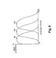
- FIG. 9is a diagram illustrating dopant concentration in a FinFET as a function of vertical depth
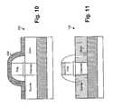
- FIGS. 10 and 11are cross-sectional views taken along the line B-B′ in FIG. 1;
- FIGS. 12A and 12Bare cross-sectional views illustrating the application of a spin-on-glass layer prior to gate patterning.
- FIGS. 13A-13Care cross-sectional views that illustrate the formation of multiple fins for a FinFET.
- a FinFETis described that has a relatively uniform dopant concentration in the source/drain junction.
- the uniform dopant concentrationis achieved through multiple tilted implantations.
- the uniform dopant concentrationcan be advantageous as it may provide for uniform channel length along the width and better short channel control.
- FIG. 1is a top-level view of a FinFET 100 consistent with principles of the invention.
- FinFET 100includes a source region 101 , a drain region 102 , a gate 104 , and a fin 103 .
- the portion of fin 103 that is under gate 104is the channel for the transistor.
- FIGS. 2 and 3are cross-sectional views taken along the line A-A′ in FIG. 1 .
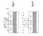
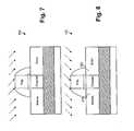
- FIGS. 5-8are cross-sectional views taken along the line B-B′ in FIG. 1 .
- FIGS. 2, 3 , and 5 - 8each illustrate steps in the manufacturing process of FinFET 100 .
- FinFET 100may be a silicon on insulator (SOI) device that includes a silicon substrate 210 and a buried oxide (BOX) layer 220 disposed on the silicon substrate 210 .
- Substrate 210may alternatively comprise germanium, metals, or combinations of such materials, such as silicon-germanium.
- Buried oxide layer 220may be formed on silicon substrate 210 in a conventional manner.
- a silicon layermay be disposed on BOX layer 220 and etched to create the source, drain, and fin 225 (source and drain not shown in FIG. 2 ).
- source/drain regions 101 and 102may be formed by depositing silicon and etching the silicon after the fin 225 is formed.
- fin 225may range from, for example, approximately 10 nm to about 30 nm in width.
- a silicon dioxide (SiO 2 ) or silicon nitride (Si 3 N 4 ) layer 230may be deposited via chemical vapor deposition (CVD) on fin 225 .
- Layer 230protects fin 225 during the fabrication process, and may be, for example, deposited to a thickness ranging from about 10 nm to 20 nm.
- gate dielectric layers 235may be grown on the side surfaces of fin 225 .
- the width of gate dielectric layers 235may range from about 0.8 to about 2 nm.
- FIG. 3is a cross-sectional view of FinFET 100 after deposition of gate material layer 250 .
- Gate material layer 250may be polysilicon or another similar type of material. This layer forms the portion of gate 104 that overlaps fin 103 .
- Layer 250may be deposited via, for example, CVD to a depth of approximately 70 nm.
- FIG. 4is a perspective view illustrating FinFET 100 as shown in FIGS. 1 and 2.
- Source 101 , drain 102 , and fin 103 of FinFET 100are shown in FIG. 3 .
- Darkened area 301represents the area at which the gate material layer 250 is deposited.
- the direction of the vertical depth within the MOSFET, as used herein,is shown by line 310 .
- FIG. 5is a cross-sectional view taken along the line B-B′ in FIG. 1 .
- SiO 2 spacers 240may be formed around gate material layer 250 . Spacers 240 protect the channel area during implantation of source 101 and drain 102 .
- FinFET 100may be implanted with a dopant to dope source 101 and drain 102 .
- the dopantmay be, for example, As + or P + .
- the dopantmay be, for example, B or BF 2 .
- the selected dopantmay be deposited in a number of different implantation operations that are set at different tilt angles.
- a dopantmay be implanted on FinFET 100 in which the ions beams are directed orthogonally to BOX layer 220 (i.e., at a tile angle of approximately zero degrees) using an ion beam with the energy that is determined by the fin height and dopant species.
- the dopantmay then be implanted at a different tilt angle (FIG. 7) and then at yet another tile angle (FIG. 8 ).
- the tilt angles shown in FIGS. 7 and 8are complimentary angles, such as 45 degrees and 135 degrees.
- the ion beam for implanting the dopant in FIGS. 7 and 8may have an energy between approximately 10 keV and 15 keV for phosphorus and between 4 keV and 6 keV for boron for the 65 nm fin height.
- the source 270 junction (FIG. 8) and the drain junction 280 (FIG. 8)are doped relatively uniformly in the vertical direction. This can be advantageous, as it provides for well defined channel length along the width and better short channel control.
- FIG. 9is a diagram illustrating dopant concentration in the source/drain 101 / 102 as a function of vertical depth 310 within the fin 225 .
- Curves 901 , 902 and 903represent dopant concentration levels at various depths within FinFET 100 caused by the first, second, and third implantations. Specifically, curve 901 represents dopant concentration caused by the implantation shown in FIG. 6, curve 902 represents dopant concentration caused by the implantation shown in FIG. 7, and curve 903 represents dopant concentration caused by the implantation shown in FIG. 8 . As can be seen, due to the multiple tilted implantations, the total dopant concentration along the vertical depth of fin 225 is more uniform than with a single implantation.
- a metal layer 260may next be deposited on FinFET 100 .
- Metal layer 260may be, for example, tungsten, cobalt, titanium, tantalum, or molybdenum.
- Metal layer 260may then be thermally annealed to create a metal silicide compound.
- FIG. 11illustrates FinFET 100 after silicidation, in which the silicided areas are shown by vertical cross-hatching.
- gate 104may be patterned.
- One way to prepare gate 104 for patterningis to first apply a spin-on-glass (SOG) layer to polysilicon 250 .
- SOGis a known interlevel dielectric material that can be applied to a silicon wafer in liquid form.
- FIGS. 12A and 12Billustrate the application of a SOG layer prior to gate patteming.
- SOG layer 1201is applied over polysilicon layer 250 .
- SOG layer 1201may then be etched back to the level of polysilicon 250 (FIG. 12 B).
- gate 104can be patterned over the exposed polysilicon.
- FIGS. 13A-13Care cross-sectional views taken along a line such as line A-A′ (FIG. 1) that illustrate the formation of multiple fins for a FinFET.
- An oxide layermay first be deposited, patterned, and etched to form oxide “fins” 1301 (FIG. 13 A). Silicon may then be deposited in the spaces between oxide “fins” 1302 and planarized (FIG. 13B) to produce silicon fins 1302 . The oxide may then be selectively etched away, leaving only the silicon fins 1302 (FIG. 13 C).
- the FinFET described abovehas a relatively uniform dopant concentration in the source/drain junction.
- the uniform dopant concentrationis achieved through multiple tilted implantations.
- the dielectric and conductive layers used in manufacturing a semiconductor device in accordance with the present inventioncan be deposited by conventional deposition techniques.
- metallization techniquessuch as various types of chemical vapor deposition (CVD) processes, including low pressure chemical vapor deposition (LPCVD) and enhanced chemical vapor deposition (ECVD) can be employed.
- CVDchemical vapor deposition
- LPCVDlow pressure chemical vapor deposition
- ECVDenhanced chemical vapor deposition
- the present inventionis applicable in the manufacturing of semiconductor devices and particularly in semiconductor devices with design features of 100 nm and below, resulting in increased transistor and circuit speeds and improved reliability.
- the present inventionis applicable to the formation of any of various types of semiconductor devices, and hence, details have not been set forth in order to avoid obscuring the thrust of the present invention.
- conventional photolithographic and etching techniquesmay be employed and, hence, the details of such techniques have not been set forth herein in detail.
Landscapes
- Physics & Mathematics (AREA)
- Engineering & Computer Science (AREA)
- High Energy & Nuclear Physics (AREA)
- General Physics & Mathematics (AREA)
- Health & Medical Sciences (AREA)
- Toxicology (AREA)
- Chemical & Material Sciences (AREA)
- Condensed Matter Physics & Semiconductors (AREA)
- Crystallography & Structural Chemistry (AREA)
- Manufacturing & Machinery (AREA)
- Computer Hardware Design (AREA)
- Microelectronics & Electronic Packaging (AREA)
- Power Engineering (AREA)
- Thin Film Transistor (AREA)
- Insulated Gate Type Field-Effect Transistor (AREA)
Abstract
Description
A. Field of the Invention
The present invention relates generally to semiconductor manufacturing and semiconductor devices and, more particularly, to double gate metal-oxide semiconductor field-effect transistors (MOSFETs).
B. Description of Related Art
Transistors, such as MOSFETs, are the core building block of the vast majority of semiconductor devices. Some semiconductor devices, such as high performance processors, can include millions of transistors. For these devices, decreasing transistor size, and thus increasing transistor density, has traditionally been a high priority in the semiconductor manufacturing area.
Conventional MOSFETs have difficulty scaling below 50 nm fabrication processing. To develop sub-50 nm MOSFETs, double-gate MOSFETs have been proposed. In several respects, the double-gate MOSFETs offer better characteristics than the conventional bulk silicon MOSFETs. These improvements arise because the double-gate MOSFET has a gate electrode on both sides of the channel, rather than only on one side as in conventional MOSFETs. When there are two gates, the electric field generated by the drain is better screened from the source end of the channel. Also, two gates can control roughly twice as much current as a single gate, resulting in a stronger switching signal.
A FinFET, as the term is used herein, refers to a type of double-gate MOSFET in which a conducting channel is formed in a vertical Si “fin” controlled by a self-aligned double-gate. FinFETs are known in the art. FinFETs tend to scale well to small device dimensions and may thus be desirable when designing semiconductor integrated circuits.
Implementations consistent with the present invention include a FinFET having vertically uniform dopant concentrations in the source/drain junction, and methods of manufacturing the same.
One aspect of the invention is directed to a method for forming a MOSFET. The method includes forming a source, a drain, and a fin structure on an insulating layer, portions of the fin structure acting as a channel for the MOSFET. The method further includes performing a first implantation with a first dopant of the source and the drain; and performing a second implantation with the first dopant of the source and the drain, the second implantation being performed at a tilt angle different than a tilt angle of the first implantation.
In another implementation consistent with principles of the invention, a method includes forming a source, a drain, and a fin structure on an insulating layer, portions of the fin structure acting as a channel for the MOSFET. The method further includes implanting the source and the drain with a first dopant using a number of implantation steps in which each of the implantation steps is performed at different tilt angles, wherein the implantation steps cause a concentration of the first dopant to be substantially uniform along a vertical depth of a junction of the source and the drain.
Reference is made to the attached drawings, wherein elements having the same reference number designation may represent like elements throughout.
FIG. 1 is a top-level view of a FinFET;
FIGS. 2 and 3 are cross-sectional views of the FinFET of FIG. 1 taken along the line A-A′;
FIG. 4 is a perspective view illustrating the FinFET shown in FIGS. 1-3;
FIGS. 5-8 are cross-sectional views taken along the line B-B′ in FIG. 1;
FIG. 9 is a diagram illustrating dopant concentration in a FinFET as a function of vertical depth;
FIGS. 10 and 11 are cross-sectional views taken along the line B-B′ in FIG. 1;
FIGS. 12A and 12B are cross-sectional views illustrating the application of a spin-on-glass layer prior to gate patterning; and
FIGS. 13A-13C are cross-sectional views that illustrate the formation of multiple fins for a FinFET.
The following detailed description of the invention refers to the accompanying drawings. The same reference numbers may be used in different drawings to identify the same or similar elements. Also, the following detailed description does not limit the invention. Instead, the scope of the invention is defined by the appended claims and equivalents.
A FinFET is described that has a relatively uniform dopant concentration in the source/drain junction. The uniform dopant concentration is achieved through multiple tilted implantations. The uniform dopant concentration can be advantageous as it may provide for uniform channel length along the width and better short channel control.
FIG. 1 is a top-level view of a FinFET100 consistent with principles of the invention. FinFET100 includes asource region 101, adrain region 102, agate 104, and afin 103. The portion offin 103 that is undergate 104 is the channel for the transistor. FIGS. 2 and 3 are cross-sectional views taken along the line A-A′ in FIG.1. FIGS. 5-8 are cross-sectional views taken along the line B-B′ in FIG.1. FIGS. 2,3, and5-8 each illustrate steps in the manufacturing process of FinFET100.
Referring to FIG. 2, FinFET100 may be a silicon on insulator (SOI) device that includes asilicon substrate 210 and a buried oxide (BOX)layer 220 disposed on thesilicon substrate 210.Substrate 210 may alternatively comprise gernanium, metals, or combinations of such materials, such as silicon-germanium. Buriedoxide layer 220 may be formed onsilicon substrate 210 in a conventional manner.
A silicon layer may be disposed onBOX layer 220 and etched to create the source, drain, and fin225 (source and drain not shown in FIG.2). Alternatively, source/drain regions fin 225 is formed. In one implementation,fin 225 may range from, for example, approximately 10 nm to about 30 nm in width. Before etchingfin 225, a silicon dioxide (SiO2) or silicon nitride (Si3N4)layer 230 may be deposited via chemical vapor deposition (CVD) onfin 225.Layer 230 protects fin225 during the fabrication process, and may be, for example, deposited to a thickness ranging from about 10 nm to 20 nm.
By oxidizing the silicon surface offin 225, gatedielectric layers 235 may be grown on the side surfaces offin 225. The width of gatedielectric layers 235 may range from about 0.8 to about 2 nm.
FIG. 3 is a cross-sectional view ofFinFET 100 after deposition ofgate material layer 250.Gate material layer 250 may be polysilicon or another similar type of material. This layer forms the portion ofgate 104 that overlaps fin103.Layer 250 may be deposited via, for example, CVD to a depth of approximately 70 nm.
FIG. 4 is a perspective view illustrating FinFET100 as shown in FIGS. 1 and 2.Source 101,drain 102, andfin 103 of FinFET100 are shown in FIG.3.Darkened area 301 represents the area at which thegate material layer 250 is deposited. The direction of the vertical depth within the MOSFET, as used herein, is shown byline 310.
FIG. 5 is a cross-sectional view taken along the line B-B′ in FIG.1. As shown in FIG. 5, SiO2spacers240 may be formed aroundgate material layer 250.Spacers 240 protect the channel area during implantation ofsource 101 and drain102.
At this point,FinFET 100 may be implanted with a dopant todope source 101 and drain102. For a NMOS device, the dopant may be, for example, As+ or P+. For a PMOS device, the dopant may be, for example, B or BF2. Consistent with an aspect of the present invention, the selected dopant may be deposited in a number of different implantation operations that are set at different tilt angles.
Referring to FIG. 6, a dopant may be implanted onFinFET 100 in which the ions beams are directed orthogonally to BOX layer220 (i.e., at a tile angle of approximately zero degrees) using an ion beam with the energy that is determined by the fin height and dopant species. For example, with 65 nm fin height, 20 keV phosphorus implant can be used for n+ junction and 8 keV boron can be used for p+ junction. The dopant may then be implanted at a different tilt angle (FIG. 7) and then at yet another tile angle (FIG.8). In one embodiment, the tilt angles shown in FIGS. 7 and 8 are complimentary angles, such as 45 degrees and 135 degrees. The ion beam for implanting the dopant in FIGS. 7 and 8 may have an energy between approximately 10 keV and 15 keV for phosphorus and between 4 keV and 6 keV for boron for the 65 nm fin height.
By implanting at multiple angles, as shown in FIGS. 6-8, thesource 270 junction (FIG. 8) and the drain junction280 (FIG. 8) are doped relatively uniformly in the vertical direction. This can be advantageous, as it provides for well defined channel length along the width and better short channel control.
One of ordinary skill in the art will recognize that various tilt angles used in implantingFinFET 100 may be used in addition to that shown in FIGS. 6-8. Similarly, although three implantation operations are illustrated, in other implementations, two implantation operations or more than three implantation operations may be used.
FIG. 9 is a diagram illustrating dopant concentration in the source/drain 101/102 as a function ofvertical depth 310 within thefin 225.Curves FinFET 100 caused by the first, second, and third implantations. Specifically,curve 901 represents dopant concentration caused by the implantation shown in FIG. 6,curve 902 represents dopant concentration caused by the implantation shown in FIG. 7, andcurve 903 represents dopant concentration caused by the implantation shown in FIG.8. As can be seen, due to the multiple tilted implantations, the total dopant concentration along the vertical depth offin 225 is more uniform than with a single implantation.
Referring to FIG. 10, ametal layer 260 may next be deposited onFinFET 100.Metal layer 260 may be, for example, tungsten, cobalt, titanium, tantalum, or molybdenum.Metal layer 260 may then be thermally annealed to create a metal silicide compound. FIG. 11 illustratesFinFET 100 after silicidation, in which the silicided areas are shown by vertical cross-hatching.
Additional Disclosure
After applying polysilicon layer250 (FIG.3),gate 104 may be patterned. One way to preparegate 104 for patterning is to first apply a spin-on-glass (SOG) layer topolysilicon 250. SOG is a known interlevel dielectric material that can be applied to a silicon wafer in liquid form.
FIGS. 12A and 12B illustrate the application of a SOG layer prior to gate patteming. As shown in FIG. 12A,SOG layer 1201 is applied overpolysilicon layer 250.SOG layer 1201 may then be etched back to the level of polysilicon250 (FIG.12B). At this point,gate 104 can be patterned over the exposed polysilicon.
In some FinFETs, it may be desirable to have more than one fin. FIGS. 13A-13C are cross-sectional views taken along a line such as line A-A′ (FIG. 1) that illustrate the formation of multiple fins for a FinFET. An oxide layer may first be deposited, patterned, and etched to form oxide “fins”1301 (FIG.13A). Silicon may then be deposited in the spaces between oxide “fins”1302 and planarized (FIG. 13B) to producesilicon fins 1302. The oxide may then be selectively etched away, leaving only the silicon fins1302 (FIG.13C).
The FinFET described above has a relatively uniform dopant concentration in the source/drain junction. The uniform dopant concentration is achieved through multiple tilted implantations.
In the previous descriptions, numerous specific details are set forth, such as specific materials, structures, chemicals, processes, etc., in order to provide a thorough understanding of the present invention. However, the present invention can be practiced without resorting to the specific details set forth herein. In other instances, well known processing structures have not been described in detail, in order not to unnecessarily obscure the thrust of the present invention.
The dielectric and conductive layers used in manufacturing a semiconductor device in accordance with the present invention can be deposited by conventional deposition techniques. For example, metallization techniques, such as various types of chemical vapor deposition (CVD) processes, including low pressure chemical vapor deposition (LPCVD) and enhanced chemical vapor deposition (ECVD) can be employed.
The present invention is applicable in the manufacturing of semiconductor devices and particularly in semiconductor devices with design features of 100 nm and below, resulting in increased transistor and circuit speeds and improved reliability. The present invention is applicable to the formation of any of various types of semiconductor devices, and hence, details have not been set forth in order to avoid obscuring the thrust of the present invention. In practicing the present invention, conventional photolithographic and etching techniques may be employed and, hence, the details of such techniques have not been set forth herein in detail.
Only the preferred embodiments of the invention and a few examples of its versatility are shown and described in the present disclosure. It is to be understood that the invention is capable of use in various other combinations and environments and is capable of modification within the scope of the inventive concept as expressed herein.
Claims (20)
1. A method for forming a MOSFET comprising:
forming a source, a drain, and a fin structure on an insulating layer, portions of the fin structure acting as a channel for the MOSFET;
performing a first implantation with a dopant of the source and the drain; and
performing a second implantation with the dopant of the source and the drain, the second implantation being performed at a tilt angle different than a tilt angle of the first implantation and in a same region of the source and drain as the first implantation.
2. The method ofclaim 1 , further comprising:
performing a third implantation with the dopant at a tilt angle different than the tilt angle of the first implantation and the second implantation and in the same region of the source and drain as the first and second implantations.
3. The method ofclaim 2 , wherein the second and third tilt angles are complimentary to one another.
4. The method ofclaim 1 , further comprising:
performing one or more additional implantations with the dopant at tilt angles that are different than the tilt angles of the first implantation and the second implantation and in the same region of the source and drain as the first and second implantations.
5. The method ofclaim 1 , wherein the dopant is an n-type dopant.
6. The method ofclaim 1 , wherein the dopant is a p-type dopant.
7. The method ofclaim 1 , wherein the first implantation deposits the dopant at a tilt angle of approximately zero degrees.
8. The method ofclaim 7 , wherein the second implantation deposits the dopant at a tilt angle of approximately 45 degrees.
9. The method ofclaim 8 , wherein the first implantation is performed using an ion beam implantation technique at approximately 20 keV and the second implantation is performed using an ion beam implantation technique at approximately 15 keV.
10. The method ofclaim 1 , further comprising:
forming SiO2spacers around the fin structure prior to performing the first implantation and the second implantation.
11. The method ofclaim 1 , wherein the MOSFET is a FinFET.
12. A method comprising:
forming a source, a drain, and a fin structure on an insulating layer, portions of the fin structure acting as a channel for the MOSFET; and
implanting the source and the drain with a dopant using a plurality of implantation steps in which each of the plurality of implantation steps is performed at a different tilt angle and in a same region of the source and drain, wherein
the plurality of implantation steps cause a concentration of the dopant to be substantially uniform along a vertical depth of a junction of the source and the drain.
13. The method ofclaim 12 , wherein the plurality of implantation steps includes three implantation steps.
14. The method ofclaim 12 , wherein a first of the plurality of implantation steps is performed at a tilt angle of approximately zero degrees.
15. The method ofclaim 14 , wherein a second of the implantation steps is performed at a tilt angle of approximately 45 degrees.
16. The method ofclaim 15 , wherein a third of the implantation steps is performed at a tilt angle complimentary to the tilt angle of the second of the implantation steps.
17. The method ofclaim 15 , wherein the first implantation step is performed using an ion beam implantation technique at approximately 20 keV and the second implantation step is preformed using an ion beam implantation technique at approximately 15 keV.
18. The method ofclaim 12 , wherein the dopant is one of As+ or P+.
19. The method ofclaim 12 , wherein the dopant is one of B or BF2.
20. The method ofclaim 12 , further comprising:
forming SiO2spacers around the fin structure prior to the implanting the source and the drain.
Priority Applications (1)
| Application Number | Priority Date | Filing Date | Title |
|---|---|---|---|
| US10/385,692US6716690B1 (en) | 2003-03-12 | 2003-03-12 | Uniformly doped source/drain junction in a double-gate MOSFET |
Applications Claiming Priority (1)
| Application Number | Priority Date | Filing Date | Title |
|---|---|---|---|
| US10/385,692US6716690B1 (en) | 2003-03-12 | 2003-03-12 | Uniformly doped source/drain junction in a double-gate MOSFET |
Publications (1)
| Publication Number | Publication Date |
|---|---|
| US6716690B1true US6716690B1 (en) | 2004-04-06 |
Family
ID=32030593
Family Applications (1)
| Application Number | Title | Priority Date | Filing Date |
|---|---|---|---|
| US10/385,692Expired - LifetimeUS6716690B1 (en) | 2003-03-12 | 2003-03-12 | Uniformly doped source/drain junction in a double-gate MOSFET |
Country Status (1)
| Country | Link |
|---|---|
| US (1) | US6716690B1 (en) |
Cited By (45)
| Publication number | Priority date | Publication date | Assignee | Title |
|---|---|---|---|---|
| US20040036126A1 (en)* | 2002-08-23 | 2004-02-26 | Chau Robert S. | Tri-gate devices and methods of fabrication |
| US20050156171A1 (en)* | 2003-12-30 | 2005-07-21 | Brask Justin K. | Nonplanar transistors with metal gate electrodes |
| US20050158970A1 (en)* | 2004-01-16 | 2005-07-21 | Robert Chau | Tri-gate transistors and methods to fabricate same |
| US20050218438A1 (en)* | 2004-03-31 | 2005-10-06 | Nick Lindert | Bulk non-planar transistor having strained enhanced mobility and methods of fabrication |
| US20050242406A1 (en)* | 2003-06-27 | 2005-11-03 | Hareland Scott A | Nonplanar device with stress incorporation layer and method of fabrication |
| US20050266692A1 (en)* | 2004-06-01 | 2005-12-01 | Brask Justin K | Method of patterning a film |
| US20060033095A1 (en)* | 2004-08-10 | 2006-02-16 | Doyle Brian S | Non-planar pMOS structure with a strained channel region and an integrated strained CMOS flow |
| US20060063332A1 (en)* | 2004-09-23 | 2006-03-23 | Brian Doyle | U-gate transistors and methods of fabrication |
| US20060068591A1 (en)* | 2004-09-29 | 2006-03-30 | Marko Radosavljevic | Fabrication of channel wraparound gate structure for field-effect transistor |
| US20060086977A1 (en)* | 2004-10-25 | 2006-04-27 | Uday Shah | Nonplanar device with thinned lower body portion and method of fabrication |
| US20060128131A1 (en)* | 2004-09-29 | 2006-06-15 | Chang Peter L | Independently accessed double-gate and tri-gate transistors in same process flow |
| US20060138553A1 (en)* | 2004-09-30 | 2006-06-29 | Brask Justin K | Nonplanar transistors with metal gate electrodes |
| US20060157794A1 (en)* | 2005-01-18 | 2006-07-20 | Doyle Brian S | Non-planar MOS structure with a strained channel region |
| US20060172497A1 (en)* | 2003-06-27 | 2006-08-03 | Hareland Scott A | Nonplanar semiconductor device with partially or fully wrapped around gate electrode and methods of fabrication |
| US20060186484A1 (en)* | 2005-02-23 | 2006-08-24 | Chau Robert S | Field effect transistor with narrow bandgap source and drain regions and method of fabrication |
| US20060202266A1 (en)* | 2005-03-14 | 2006-09-14 | Marko Radosavljevic | Field effect transistor with metal source/drain regions |
| US20060223302A1 (en)* | 2005-03-31 | 2006-10-05 | Chang Peter L | Self-aligned contacts for transistors |
| US20060234431A1 (en)* | 2003-04-29 | 2006-10-19 | Yee-Chia Yeo | Doping of semiconductor fin devices |
| US20060286755A1 (en)* | 2005-06-15 | 2006-12-21 | Brask Justin K | Method for fabricating transistor with thinned channel |
| US20070001173A1 (en)* | 2005-06-21 | 2007-01-04 | Brask Justin K | Semiconductor device structures and methods of forming semiconductor structures |
| US20070001219A1 (en)* | 2005-06-30 | 2007-01-04 | Marko Radosavljevic | Block contact architectures for nanoscale channel transistors |
| US20070078193A1 (en)* | 2005-08-31 | 2007-04-05 | Gilder Stephen D | Strut-reinforced, reduced VOC polyurethane foam |
| US20070090416A1 (en)* | 2005-09-28 | 2007-04-26 | Doyle Brian S | CMOS devices with a single work function gate electrode and method of fabrication |
| US20070148837A1 (en)* | 2005-12-27 | 2007-06-28 | Uday Shah | Method of fabricating a multi-cornered film |
| US20070238273A1 (en)* | 2006-03-31 | 2007-10-11 | Doyle Brian S | Method of ion implanting for tri-gate devices |
| US20080001236A1 (en)* | 2006-06-28 | 2008-01-03 | Change Peter L D | Method of forming a transistor having gate protection and transistor formed according to the method |
| US20080160684A1 (en)* | 2004-06-29 | 2008-07-03 | Samsung Electronics Co., Ltd. | Method of fabricating multi-gate transistor and multi-gate transistor fabricated thereby |
| US7402875B2 (en) | 2005-08-17 | 2008-07-22 | Intel Corporation | Lateral undercut of metal gate in SOI device |
| US20080296702A1 (en)* | 2007-05-30 | 2008-12-04 | Tsung-Lin Lee | Integrated circuit structures with multiple FinFETs |
| US7479421B2 (en) | 2005-09-28 | 2009-01-20 | Intel Corporation | Process for integrating planar and non-planar CMOS transistors on a bulk substrate and article made thereby |
| US20090121291A1 (en)* | 2007-11-14 | 2009-05-14 | Anderson Brent A | Dense chevron non-planar field effect transistors and method |
| US20090256207A1 (en)* | 2008-04-14 | 2009-10-15 | International Business Machines Corporation | Finfet devices from bulk semiconductor and methods for manufacturing the same |
| US20100065888A1 (en)* | 2004-06-30 | 2010-03-18 | Shaheen Mohamad A | High mobility tri-gate devices and methods of fabrication |
| US20110129978A1 (en)* | 2009-12-01 | 2011-06-02 | Kangguo Cheng | Method and structure for forming finfets with multiple doping regions on a same chip |
| US20110127588A1 (en)* | 2009-12-01 | 2011-06-02 | International Business Machines Corporation | Enhancing mosfet performance by optimizing stress properties |
| US7989280B2 (en) | 2005-11-30 | 2011-08-02 | Intel Corporation | Dielectric interface for group III-V semiconductor device |
| US8362566B2 (en) | 2008-06-23 | 2013-01-29 | Intel Corporation | Stress in trigate devices using complimentary gate fill materials |
| US20130193481A1 (en)* | 2012-01-27 | 2013-08-01 | International Business Machines Corporation | Field effect transistor and a method of forming the transistor |
| US8617945B2 (en) | 2006-08-02 | 2013-12-31 | Intel Corporation | Stacking fault and twin blocking barrier for integrating III-V on Si |
| US20140329367A1 (en)* | 2006-11-06 | 2014-11-06 | Cree, Inc. | Methods of fabricating semiconductor devices including implanted regions for providing low-resistance contact to buried layers and related devices |
| US8946031B2 (en) | 2012-01-18 | 2015-02-03 | United Microelectronics Corp. | Method for fabricating MOS device |
| US9449963B2 (en)* | 2014-07-03 | 2016-09-20 | Taiwan Semiconductor Manufacturing Co., Ltd. | Gate structure with hard mask structure formed thereon and method for forming the same |
| US20170213830A1 (en)* | 2013-05-23 | 2017-07-27 | Taiwan Semiconductor Manufacturing Company, Ltd. | Tuning Tensile Strain on FinFET |
| US10529831B1 (en) | 2018-08-03 | 2020-01-07 | Globalfoundries Inc. | Methods, apparatus, and system for forming epitaxial formations with reduced risk of merging |
| CN113270419A (en)* | 2020-02-16 | 2021-08-17 | 北京元芯碳基集成电路研究院 | Undoped semiconductor device for SoC and manufacturing method thereof |
Citations (12)
| Publication number | Priority date | Publication date | Assignee | Title |
|---|---|---|---|---|
| US5500379A (en)* | 1993-06-25 | 1996-03-19 | Matsushita Electric Industrial Co., Ltd. | Method of manufacturing semiconductor device |
| US5516711A (en)* | 1994-12-16 | 1996-05-14 | Mosel Vitelic, Inc. | Method for forming LDD CMOS with oblique implantation |
| US5750435A (en)* | 1995-07-26 | 1998-05-12 | Chartered Semiconductor Manufacturing Company Ltd. | Method for minimizing the hot carrier effect in N-MOSFET devices |
| US5793090A (en)* | 1997-01-10 | 1998-08-11 | Advanced Micro Devices, Inc. | Integrated circuit having multiple LDD and/or source/drain implant steps to enhance circuit performance |
| US5891774A (en)* | 1995-11-17 | 1999-04-06 | Sharp Kabushiki Kaisha | Method of fabricating EEPROM using oblique implantation |
| US6083795A (en)* | 1998-02-09 | 2000-07-04 | Taiwan Semiconductor Manufacturing Company | Large angle channel threshold implant for improving reverse narrow width effect |
| US6297098B1 (en)* | 1999-11-01 | 2001-10-02 | Taiwan Semiconductor Manufacturing Company | Tilt-angle ion implant to improve junction breakdown in flash memory application |
| US6300182B1 (en)* | 2000-12-11 | 2001-10-09 | Advanced Micro Devices, Inc. | Field effect transistor having dual gates with asymmetrical doping for reduced threshold voltage |
| US6413802B1 (en)* | 2000-10-23 | 2002-07-02 | The Regents Of The University Of California | Finfet transistor structures having a double gate channel extending vertically from a substrate and methods of manufacture |
| US20020195626A1 (en)* | 2000-08-22 | 2002-12-26 | Tran Luan C. | Double LDD devices for improved DRAM refresh |
| US6509264B1 (en)* | 2000-03-30 | 2003-01-21 | Chartered Semiconductor Manufacturing Ltd. | Method to form self-aligned silicide with reduced sheet resistance |
| US6521502B1 (en)* | 2000-08-07 | 2003-02-18 | Advanced Micro Devices, Inc. | Solid phase epitaxy activation process for source/drain junction extensions and halo regions |
- 2003
- 2003-03-12USUS10/385,692patent/US6716690B1/ennot_activeExpired - Lifetime
Patent Citations (12)
| Publication number | Priority date | Publication date | Assignee | Title |
|---|---|---|---|---|
| US5500379A (en)* | 1993-06-25 | 1996-03-19 | Matsushita Electric Industrial Co., Ltd. | Method of manufacturing semiconductor device |
| US5516711A (en)* | 1994-12-16 | 1996-05-14 | Mosel Vitelic, Inc. | Method for forming LDD CMOS with oblique implantation |
| US5750435A (en)* | 1995-07-26 | 1998-05-12 | Chartered Semiconductor Manufacturing Company Ltd. | Method for minimizing the hot carrier effect in N-MOSFET devices |
| US5891774A (en)* | 1995-11-17 | 1999-04-06 | Sharp Kabushiki Kaisha | Method of fabricating EEPROM using oblique implantation |
| US5793090A (en)* | 1997-01-10 | 1998-08-11 | Advanced Micro Devices, Inc. | Integrated circuit having multiple LDD and/or source/drain implant steps to enhance circuit performance |
| US6083795A (en)* | 1998-02-09 | 2000-07-04 | Taiwan Semiconductor Manufacturing Company | Large angle channel threshold implant for improving reverse narrow width effect |
| US6297098B1 (en)* | 1999-11-01 | 2001-10-02 | Taiwan Semiconductor Manufacturing Company | Tilt-angle ion implant to improve junction breakdown in flash memory application |
| US6509264B1 (en)* | 2000-03-30 | 2003-01-21 | Chartered Semiconductor Manufacturing Ltd. | Method to form self-aligned silicide with reduced sheet resistance |
| US6521502B1 (en)* | 2000-08-07 | 2003-02-18 | Advanced Micro Devices, Inc. | Solid phase epitaxy activation process for source/drain junction extensions and halo regions |
| US20020195626A1 (en)* | 2000-08-22 | 2002-12-26 | Tran Luan C. | Double LDD devices for improved DRAM refresh |
| US6413802B1 (en)* | 2000-10-23 | 2002-07-02 | The Regents Of The University Of California | Finfet transistor structures having a double gate channel extending vertically from a substrate and methods of manufacture |
| US6300182B1 (en)* | 2000-12-11 | 2001-10-09 | Advanced Micro Devices, Inc. | Field effect transistor having dual gates with asymmetrical doping for reduced threshold voltage |
Non-Patent Citations (6)
| Title |
|---|
| Digh Hisamoto et al.: "FinFET-A Self-Aligned Double-Gate MOSFET Scalable to 20 nm," IEEE Transactions on Electron Devices, vol. 47, No. 12, Dec. 2000, pp. 2320-2325. |
| Digh Hisamoto et al.: "FinFET—A Self-Aligned Double-Gate MOSFET Scalable to 20 nm," IEEE Transactions on Electron Devices, vol. 47, No. 12, Dec. 2000, pp. 2320-2325. |
| Xuejue Huang et al.: "Sub-50 nm P-Channel Fin FET," IEEE Transactions on Electron Devices, vol. 48, No. 5, May 2001, pp. 880-886. |
| Yang-Kyu Choi et al.: "Nanoscale CMOS Spacer FINFET for the Terabit Era," IEEE Electron Device Letters, vol. 23, No. 1, Jan. 2002, pp. 25-27. |
| Yang-Kyu Choi et al.: "Sub-20nm CMOS Fin FET Technologies," 0-7803-5410-9/99 IEEE, Mar. 2001, 4 pages. |
| Zuejue Huang et al.: "Sub 50-nm FInFET: PMOS," 0-7803-7050-3/01 IEEE, Sep. 1999 4 pages. |
Cited By (136)
| Publication number | Priority date | Publication date | Assignee | Title |
|---|---|---|---|---|
| US20040036126A1 (en)* | 2002-08-23 | 2004-02-26 | Chau Robert S. | Tri-gate devices and methods of fabrication |
| US20040094807A1 (en)* | 2002-08-23 | 2004-05-20 | Chau Robert S. | Tri-gate devices and methods of fabrication |
| US7514346B2 (en) | 2002-08-23 | 2009-04-07 | Intel Corporation | Tri-gate devices and methods of fabrication |
| US20060228840A1 (en)* | 2002-08-23 | 2006-10-12 | Chau Robert S | Tri-gate devices and methods of fabrication |
| US20070034972A1 (en)* | 2002-08-23 | 2007-02-15 | Chau Robert S | Tri-gate devices and methods of fabrication |
| US7560756B2 (en) | 2002-08-23 | 2009-07-14 | Intel Corporation | Tri-gate devices and methods of fabrication |
| US7358121B2 (en) | 2002-08-23 | 2008-04-15 | Intel Corporation | Tri-gate devices and methods of fabrication |
| US7368791B2 (en) | 2002-08-23 | 2008-05-06 | Intel Corporation | Multi-gate carbon nano-tube transistors |
| US7504678B2 (en) | 2002-08-23 | 2009-03-17 | Intel Corporation | Tri-gate devices and methods of fabrication |
| US7427794B2 (en) | 2002-08-23 | 2008-09-23 | Intel Corporation | Tri-gate devices and methods of fabrication |
| US20060234431A1 (en)* | 2003-04-29 | 2006-10-19 | Yee-Chia Yeo | Doping of semiconductor fin devices |
| US8790970B2 (en)* | 2003-04-29 | 2014-07-29 | Taiwan Semiconductor Manufacturing Company, Ltd. | Doping of semiconductor fin devices |
| US20050242406A1 (en)* | 2003-06-27 | 2005-11-03 | Hareland Scott A | Nonplanar device with stress incorporation layer and method of fabrication |
| US8273626B2 (en) | 2003-06-27 | 2012-09-25 | Intel Corporationn | Nonplanar semiconductor device with partially or fully wrapped around gate electrode and methods of fabrication |
| US7241653B2 (en) | 2003-06-27 | 2007-07-10 | Intel Corporation | Nonplanar device with stress incorporation layer and method of fabrication |
| US8405164B2 (en) | 2003-06-27 | 2013-03-26 | Intel Corporation | Tri-gate transistor device with stress incorporation layer and method of fabrication |
| US7820513B2 (en) | 2003-06-27 | 2010-10-26 | Intel Corporation | Nonplanar semiconductor device with partially or fully wrapped around gate electrode and methods of fabrication |
| US20060172497A1 (en)* | 2003-06-27 | 2006-08-03 | Hareland Scott A | Nonplanar semiconductor device with partially or fully wrapped around gate electrode and methods of fabrication |
| US7456476B2 (en) | 2003-06-27 | 2008-11-25 | Intel Corporation | Nonplanar semiconductor device with partially or fully wrapped around gate electrode and methods of fabrication |
| US7714397B2 (en) | 2003-06-27 | 2010-05-11 | Intel Corporation | Tri-gate transistor device with stress incorporation layer and method of fabrication |
| US7329913B2 (en) | 2003-12-30 | 2008-02-12 | Intel Corporation | Nonplanar transistors with metal gate electrodes |
| US20050156171A1 (en)* | 2003-12-30 | 2005-07-21 | Brask Justin K. | Nonplanar transistors with metal gate electrodes |
| US7268058B2 (en) | 2004-01-16 | 2007-09-11 | Intel Corporation | Tri-gate transistors and methods to fabricate same |
| WO2005071730A1 (en)* | 2004-01-16 | 2005-08-04 | Intel Corporation | Tri-gate transistors and mehtods to fabricate same |
| US20050158970A1 (en)* | 2004-01-16 | 2005-07-21 | Robert Chau | Tri-gate transistors and methods to fabricate same |
| US7781771B2 (en) | 2004-03-31 | 2010-08-24 | Intel Corporation | Bulk non-planar transistor having strained enhanced mobility and methods of fabrication |
| US7326634B2 (en) | 2004-03-31 | 2008-02-05 | Intel Corporation | Bulk non-planar transistor having strained enhanced mobility and methods of fabrication |
| US20050218438A1 (en)* | 2004-03-31 | 2005-10-06 | Nick Lindert | Bulk non-planar transistor having strained enhanced mobility and methods of fabrication |
| US7579280B2 (en) | 2004-06-01 | 2009-08-25 | Intel Corporation | Method of patterning a film |
| US20050266692A1 (en)* | 2004-06-01 | 2005-12-01 | Brask Justin K | Method of patterning a film |
| US7585734B2 (en)* | 2004-06-29 | 2009-09-08 | Samsung Electronics Co., Ltd. | Method of fabricating multi-gate transistor and multi-gate transistor fabricated thereby |
| US20080160684A1 (en)* | 2004-06-29 | 2008-07-03 | Samsung Electronics Co., Ltd. | Method of fabricating multi-gate transistor and multi-gate transistor fabricated thereby |
| US20100065888A1 (en)* | 2004-06-30 | 2010-03-18 | Shaheen Mohamad A | High mobility tri-gate devices and methods of fabrication |
| US8084818B2 (en) | 2004-06-30 | 2011-12-27 | Intel Corporation | High mobility tri-gate devices and methods of fabrication |
| US7960794B2 (en) | 2004-08-10 | 2011-06-14 | Intel Corporation | Non-planar pMOS structure with a strained channel region and an integrated strained CMOS flow |
| US20060033095A1 (en)* | 2004-08-10 | 2006-02-16 | Doyle Brian S | Non-planar pMOS structure with a strained channel region and an integrated strained CMOS flow |
| US7348284B2 (en) | 2004-08-10 | 2008-03-25 | Intel Corporation | Non-planar pMOS structure with a strained channel region and an integrated strained CMOS flow |
| US20060063332A1 (en)* | 2004-09-23 | 2006-03-23 | Brian Doyle | U-gate transistors and methods of fabrication |
| US8399922B2 (en) | 2004-09-29 | 2013-03-19 | Intel Corporation | Independently accessed double-gate and tri-gate transistors |
| US20060128131A1 (en)* | 2004-09-29 | 2006-06-15 | Chang Peter L | Independently accessed double-gate and tri-gate transistors in same process flow |
| US7915167B2 (en) | 2004-09-29 | 2011-03-29 | Intel Corporation | Fabrication of channel wraparound gate structure for field-effect transistor |
| US7859053B2 (en) | 2004-09-29 | 2010-12-28 | Intel Corporation | Independently accessed double-gate and tri-gate transistors in same process flow |
| US8268709B2 (en) | 2004-09-29 | 2012-09-18 | Intel Corporation | Independently accessed double-gate and tri-gate transistors in same process flow |
| US20060068591A1 (en)* | 2004-09-29 | 2006-03-30 | Marko Radosavljevic | Fabrication of channel wraparound gate structure for field-effect transistor |
| US7361958B2 (en) | 2004-09-30 | 2008-04-22 | Intel Corporation | Nonplanar transistors with metal gate electrodes |
| US7326656B2 (en) | 2004-09-30 | 2008-02-05 | Intel Corporation | Method of forming a metal oxide dielectric |
| US20060138552A1 (en)* | 2004-09-30 | 2006-06-29 | Brask Justin K | Nonplanar transistors with metal gate electrodes |
| US7531437B2 (en) | 2004-09-30 | 2009-05-12 | Intel Corporation | Method of forming metal gate electrodes using sacrificial gate electrode material and sacrificial gate dielectric material |
| US7528025B2 (en) | 2004-09-30 | 2009-05-05 | Intel Corporation | Nonplanar transistors with metal gate electrodes |
| US20060138553A1 (en)* | 2004-09-30 | 2006-06-29 | Brask Justin K | Nonplanar transistors with metal gate electrodes |
| US10236356B2 (en) | 2004-10-25 | 2019-03-19 | Intel Corporation | Nonplanar device with thinned lower body portion and method of fabrication |
| US8749026B2 (en) | 2004-10-25 | 2014-06-10 | Intel Corporation | Nonplanar device with thinned lower body portion and method of fabrication |
| US20060214231A1 (en)* | 2004-10-25 | 2006-09-28 | Uday Shah | Nonplanar device with thinned lower body portion and method of fabrication |
| US8502351B2 (en) | 2004-10-25 | 2013-08-06 | Intel Corporation | Nonplanar device with thinned lower body portion and method of fabrication |
| US7550333B2 (en) | 2004-10-25 | 2009-06-23 | Intel Corporation | Nonplanar device with thinned lower body portion and method of fabrication |
| US9190518B2 (en) | 2004-10-25 | 2015-11-17 | Intel Corporation | Nonplanar device with thinned lower body portion and method of fabrication |
| US20060086977A1 (en)* | 2004-10-25 | 2006-04-27 | Uday Shah | Nonplanar device with thinned lower body portion and method of fabrication |
| US9741809B2 (en) | 2004-10-25 | 2017-08-22 | Intel Corporation | Nonplanar device with thinned lower body portion and method of fabrication |
| US8067818B2 (en) | 2004-10-25 | 2011-11-29 | Intel Corporation | Nonplanar device with thinned lower body portion and method of fabrication |
| US7193279B2 (en) | 2005-01-18 | 2007-03-20 | Intel Corporation | Non-planar MOS structure with a strained channel region |
| US20060157687A1 (en)* | 2005-01-18 | 2006-07-20 | Doyle Brian S | Non-planar MOS structure with a strained channel region |
| US7531393B2 (en) | 2005-01-18 | 2009-05-12 | Intel Corporation | Non-planar MOS structure with a strained channel region |
| US20060157794A1 (en)* | 2005-01-18 | 2006-07-20 | Doyle Brian S | Non-planar MOS structure with a strained channel region |
| US8368135B2 (en) | 2005-02-23 | 2013-02-05 | Intel Corporation | Field effect transistor with narrow bandgap source and drain regions and method of fabrication |
| US7825481B2 (en) | 2005-02-23 | 2010-11-02 | Intel Corporation | Field effect transistor with narrow bandgap source and drain regions and method of fabrication |
| US20110121393A1 (en)* | 2005-02-23 | 2011-05-26 | Chau Robert S | Field effect transistor with narrow bandgap source and drain regions and method of fabrication |
| US9368583B2 (en) | 2005-02-23 | 2016-06-14 | Intel Corporation | Field effect transistor with narrow bandgap source and drain regions and method of fabrication |
| US7893506B2 (en) | 2005-02-23 | 2011-02-22 | Intel Corporation | Field effect transistor with narrow bandgap source and drain regions and method of fabrication |
| US7518196B2 (en) | 2005-02-23 | 2009-04-14 | Intel Corporation | Field effect transistor with narrow bandgap source and drain regions and method of fabrication |
| US8664694B2 (en) | 2005-02-23 | 2014-03-04 | Intel Corporation | Field effect transistor with narrow bandgap source and drain regions and method of fabrication |
| US9048314B2 (en) | 2005-02-23 | 2015-06-02 | Intel Corporation | Field effect transistor with narrow bandgap source and drain regions and method of fabrication |
| US8183646B2 (en) | 2005-02-23 | 2012-05-22 | Intel Corporation | Field effect transistor with narrow bandgap source and drain regions and method of fabrication |
| US20060186484A1 (en)* | 2005-02-23 | 2006-08-24 | Chau Robert S | Field effect transistor with narrow bandgap source and drain regions and method of fabrication |
| US8816394B2 (en) | 2005-02-23 | 2014-08-26 | Intel Corporation | Field effect transistor with narrow bandgap source and drain regions and method of fabrication |
| US20090142897A1 (en)* | 2005-02-23 | 2009-06-04 | Chau Robert S | Field effect transistor with narrow bandgap source and drain regions and method of fabrication |
| US20060202266A1 (en)* | 2005-03-14 | 2006-09-14 | Marko Radosavljevic | Field effect transistor with metal source/drain regions |
| US7879675B2 (en) | 2005-03-14 | 2011-02-01 | Intel Corporation | Field effect transistor with metal source/drain regions |
| US20060223302A1 (en)* | 2005-03-31 | 2006-10-05 | Chang Peter L | Self-aligned contacts for transistors |
| US7563701B2 (en) | 2005-03-31 | 2009-07-21 | Intel Corporation | Self-aligned contacts for transistors |
| US9806195B2 (en) | 2005-06-15 | 2017-10-31 | Intel Corporation | Method for fabricating transistor with thinned channel |
| US7858481B2 (en) | 2005-06-15 | 2010-12-28 | Intel Corporation | Method for fabricating transistor with thinned channel |
| US9337307B2 (en) | 2005-06-15 | 2016-05-10 | Intel Corporation | Method for fabricating transistor with thinned channel |
| US20060286755A1 (en)* | 2005-06-15 | 2006-12-21 | Brask Justin K | Method for fabricating transistor with thinned channel |
| US11978799B2 (en) | 2005-06-15 | 2024-05-07 | Tahoe Research, Ltd. | Method for fabricating transistor with thinned channel |
| US7547637B2 (en) | 2005-06-21 | 2009-06-16 | Intel Corporation | Methods for patterning a semiconductor film |
| US20070001173A1 (en)* | 2005-06-21 | 2007-01-04 | Brask Justin K | Semiconductor device structures and methods of forming semiconductor structures |
| US8581258B2 (en) | 2005-06-21 | 2013-11-12 | Intel Corporation | Semiconductor device structures and methods of forming semiconductor structures |
| US9385180B2 (en) | 2005-06-21 | 2016-07-05 | Intel Corporation | Semiconductor device structures and methods of forming semiconductor structures |
| US9761724B2 (en) | 2005-06-21 | 2017-09-12 | Intel Corporation | Semiconductor device structures and methods of forming semiconductor structures |
| US8933458B2 (en) | 2005-06-21 | 2015-01-13 | Intel Corporation | Semiconductor device structures and methods of forming semiconductor structures |
| US8071983B2 (en) | 2005-06-21 | 2011-12-06 | Intel Corporation | Semiconductor device structures and methods of forming semiconductor structures |
| US7279375B2 (en) | 2005-06-30 | 2007-10-09 | Intel Corporation | Block contact architectures for nanoscale channel transistors |
| US7898041B2 (en) | 2005-06-30 | 2011-03-01 | Intel Corporation | Block contact architectures for nanoscale channel transistors |
| US20070001219A1 (en)* | 2005-06-30 | 2007-01-04 | Marko Radosavljevic | Block contact architectures for nanoscale channel transistors |
| US7402875B2 (en) | 2005-08-17 | 2008-07-22 | Intel Corporation | Lateral undercut of metal gate in SOI device |
| US7736956B2 (en) | 2005-08-17 | 2010-06-15 | Intel Corporation | Lateral undercut of metal gate in SOI device |
| US20070078193A1 (en)* | 2005-08-31 | 2007-04-05 | Gilder Stephen D | Strut-reinforced, reduced VOC polyurethane foam |
| US8294180B2 (en) | 2005-09-28 | 2012-10-23 | Intel Corporation | CMOS devices with a single work function gate electrode and method of fabrication |
| US20090090976A1 (en)* | 2005-09-28 | 2009-04-09 | Intel Corporation | Process for integrating planar and non-planar cmos transistors on a bulk substrate and article made thereby |
| US8193567B2 (en) | 2005-09-28 | 2012-06-05 | Intel Corporation | Process for integrating planar and non-planar CMOS transistors on a bulk substrate and article made thereby |
| US20070090416A1 (en)* | 2005-09-28 | 2007-04-26 | Doyle Brian S | CMOS devices with a single work function gate electrode and method of fabrication |
| US7479421B2 (en) | 2005-09-28 | 2009-01-20 | Intel Corporation | Process for integrating planar and non-planar CMOS transistors on a bulk substrate and article made thereby |
| US7902014B2 (en) | 2005-09-28 | 2011-03-08 | Intel Corporation | CMOS devices with a single work function gate electrode and method of fabrication |
| US7989280B2 (en) | 2005-11-30 | 2011-08-02 | Intel Corporation | Dielectric interface for group III-V semiconductor device |
| US20070148837A1 (en)* | 2005-12-27 | 2007-06-28 | Uday Shah | Method of fabricating a multi-cornered film |
| US7396711B2 (en) | 2005-12-27 | 2008-07-08 | Intel Corporation | Method of fabricating a multi-cornered film |
| US7449373B2 (en)* | 2006-03-31 | 2008-11-11 | Intel Corporation | Method of ion implanting for tri-gate devices |
| US20070238273A1 (en)* | 2006-03-31 | 2007-10-11 | Doyle Brian S | Method of ion implanting for tri-gate devices |
| US7544594B2 (en) | 2006-06-28 | 2009-06-09 | Intel Corporation | Method of forming a transistor having gate protection and transistor formed according to the method |
| US20080001236A1 (en)* | 2006-06-28 | 2008-01-03 | Change Peter L D | Method of forming a transistor having gate protection and transistor formed according to the method |
| US8617945B2 (en) | 2006-08-02 | 2013-12-31 | Intel Corporation | Stacking fault and twin blocking barrier for integrating III-V on Si |
| US9984881B2 (en)* | 2006-11-06 | 2018-05-29 | Cree, Inc. | Methods of fabricating semiconductor devices including implanted regions for providing low-resistance contact to buried layers and related devices |
| US20140329367A1 (en)* | 2006-11-06 | 2014-11-06 | Cree, Inc. | Methods of fabricating semiconductor devices including implanted regions for providing low-resistance contact to buried layers and related devices |
| US20080296702A1 (en)* | 2007-05-30 | 2008-12-04 | Tsung-Lin Lee | Integrated circuit structures with multiple FinFETs |
| US8174073B2 (en) | 2007-05-30 | 2012-05-08 | Taiwan Semiconductor Manufacturing Co., Ltd. | Integrated circuit structures with multiple FinFETs |
| US20090121291A1 (en)* | 2007-11-14 | 2009-05-14 | Anderson Brent A | Dense chevron non-planar field effect transistors and method |
| US7847320B2 (en) | 2007-11-14 | 2010-12-07 | International Business Machines Corporation | Dense chevron non-planar field effect transistors and method |
| US20090256207A1 (en)* | 2008-04-14 | 2009-10-15 | International Business Machines Corporation | Finfet devices from bulk semiconductor and methods for manufacturing the same |
| US8362566B2 (en) | 2008-06-23 | 2013-01-29 | Intel Corporation | Stress in trigate devices using complimentary gate fill materials |
| US8741733B2 (en) | 2008-06-23 | 2014-06-03 | Intel Corporation | Stress in trigate devices using complimentary gate fill materials |
| US9450092B2 (en) | 2008-06-23 | 2016-09-20 | Intel Corporation | Stress in trigate devices using complimentary gate fill materials |
| US9224754B2 (en) | 2008-06-23 | 2015-12-29 | Intel Corporation | Stress in trigate devices using complimentary gate fill materials |
| US9806193B2 (en) | 2008-06-23 | 2017-10-31 | Intel Corporation | Stress in trigate devices using complimentary gate fill materials |
| US8021949B2 (en)* | 2009-12-01 | 2011-09-20 | International Business Machines Corporation | Method and structure for forming finFETs with multiple doping regions on a same chip |
| US20110129978A1 (en)* | 2009-12-01 | 2011-06-02 | Kangguo Cheng | Method and structure for forming finfets with multiple doping regions on a same chip |
| US8318570B2 (en)* | 2009-12-01 | 2012-11-27 | International Business Machines Corporation | Enhancing MOSFET performance by optimizing stress properties |
| US20110127588A1 (en)* | 2009-12-01 | 2011-06-02 | International Business Machines Corporation | Enhancing mosfet performance by optimizing stress properties |
| US8946031B2 (en) | 2012-01-18 | 2015-02-03 | United Microelectronics Corp. | Method for fabricating MOS device |
| US8759916B2 (en)* | 2012-01-27 | 2014-06-24 | International Business Machines Corporation | Field effect transistor and a method of forming the transistor |
| US20130193481A1 (en)* | 2012-01-27 | 2013-08-01 | International Business Machines Corporation | Field effect transistor and a method of forming the transistor |
| US10453842B2 (en)* | 2013-05-23 | 2019-10-22 | Taiwan Semiconductor Manufacturing Company | Tuning tensile strain on FinFET |
| US20170213830A1 (en)* | 2013-05-23 | 2017-07-27 | Taiwan Semiconductor Manufacturing Company, Ltd. | Tuning Tensile Strain on FinFET |
| US11075201B2 (en) | 2013-05-23 | 2021-07-27 | Taiwan Semiconductor Manufacturing Company, Ltd. | Tuning tensile strain on FinFET |
| US9449963B2 (en)* | 2014-07-03 | 2016-09-20 | Taiwan Semiconductor Manufacturing Co., Ltd. | Gate structure with hard mask structure formed thereon and method for forming the same |
| US10529831B1 (en) | 2018-08-03 | 2020-01-07 | Globalfoundries Inc. | Methods, apparatus, and system for forming epitaxial formations with reduced risk of merging |
| CN113270419A (en)* | 2020-02-16 | 2021-08-17 | 北京元芯碳基集成电路研究院 | Undoped semiconductor device for SoC and manufacturing method thereof |
Similar Documents
| Publication | Publication Date | Title |
|---|---|---|
| US6716690B1 (en) | Uniformly doped source/drain junction in a double-gate MOSFET | |
| US7915167B2 (en) | Fabrication of channel wraparound gate structure for field-effect transistor | |
| US7635632B2 (en) | Gate electrode for a semiconductor fin device | |
| US8476139B2 (en) | High performance MOSFET | |
| US6800885B1 (en) | Asymmetrical double gate or all-around gate MOSFET devices and methods for making same | |
| US9041125B2 (en) | Fin shape for fin field-effect transistors and method of forming | |
| US7358569B2 (en) | Semiconductor device with semiconductor layer having various thickness | |
| US6921963B2 (en) | Narrow fin FinFET | |
| US6674139B2 (en) | Inverse T-gate structure using damascene processing | |
| US6913960B2 (en) | Fin-based double poly dynamic threshold CMOS FET with spacer gate and method of fabrication | |
| US20060249799A1 (en) | Concurrent fin-fet and thick body device fabrication | |
| US6853020B1 (en) | Double-gate semiconductor device | |
| US6974983B1 (en) | Isolated FinFET P-channel/N-channel transistor pair | |
| KR20050095871A (en) | Tri-gate and gate around mosfet devices and methods for making same | |
| US6842048B2 (en) | Two transistor NOR device | |
| KR20080058341A (en) | Multiple low-k and high-k gate oxides on a single gate for low miller capacity and improved drive current | |
| JP3692039B2 (en) | Manufacturing method of field effect control type transistor | |
| US7265424B2 (en) | Fin Field-effect transistor and method for producing a fin field effect-transistor | |
| US6441434B1 (en) | Semiconductor-on-insulator body-source contact and method | |
| US20120326236A1 (en) | Multi-gate transistor having sidewall contacts | |
| US6914277B1 (en) | Merged FinFET P-channel/N-channel pair | |
| KR100951205B1 (en) | Low resistance MOSSF and low resistance MOSSFT manufacturing method | |
| CN106328537B (en) | Semiconductor device and method of manufacturing the same | |
| KR20020010918A (en) | Double gate mosfet transistor and method for the production thereof | |
| US8217450B1 (en) | Double-gate semiconductor device with gate contacts formed adjacent sidewalls of a fin |
Legal Events
| Date | Code | Title | Description |
|---|---|---|---|
| AS | Assignment | Owner name:ADVANCED MICRO DEVICES, INC., CALIFORNIA Free format text:ASSIGNMENT OF ASSIGNORS INTEREST;ASSIGNORS:WANG, HAIHONG;AN, JUDY XILIN;YU, BIN;REEL/FRAME:013870/0668;SIGNING DATES FROM 20021121 TO 20030110 | |
| FEPP | Fee payment procedure | Free format text:PAYOR NUMBER ASSIGNED (ORIGINAL EVENT CODE: ASPN); ENTITY STATUS OF PATENT OWNER: LARGE ENTITY | |
| STCF | Information on status: patent grant | Free format text:PATENTED CASE | |
| FPAY | Fee payment | Year of fee payment:4 | |
| FPAY | Fee payment | Year of fee payment:8 | |
| FPAY | Fee payment | Year of fee payment:12 |