US6713824B1 - Reliable semiconductor device and method of manufacturing the same - Google Patents
Reliable semiconductor device and method of manufacturing the sameDownload PDFInfo
- Publication number
- US6713824B1 US6713824B1US09/459,913US45991399AUS6713824B1US 6713824 B1US6713824 B1US 6713824B1US 45991399 AUS45991399 AUS 45991399AUS 6713824 B1US6713824 B1US 6713824B1
- Authority
- US
- United States
- Prior art keywords
- film
- insulating film
- gate insulating
- gate electrode
- stress
- Prior art date
- Legal status (The legal status is an assumption and is not a legal conclusion. Google has not performed a legal analysis and makes no representation as to the accuracy of the status listed.)
- Expired - Fee Related
Links
- 239000004065semiconductorSubstances0.000titleclaimsabstractdescription73
- 238000004519manufacturing processMethods0.000titleabstractdescription9
- 229910021420polycrystalline siliconInorganic materials0.000claimsabstractdescription79
- 229920005591polysiliconPolymers0.000claimsabstractdescription79
- 230000015572biosynthetic processEffects0.000claimsabstractdescription31
- 230000015556catabolic processEffects0.000claimsabstractdescription9
- 239000000758substrateSubstances0.000claimsdescription53
- VYPSYNLAJGMNEJ-UHFFFAOYSA-NSilicium dioxideChemical compoundO=[Si]=OVYPSYNLAJGMNEJ-UHFFFAOYSA-N0.000claimsdescription13
- 238000000034methodMethods0.000claimsdescription10
- 229910052814silicon oxideInorganic materials0.000claimsdescription9
- 230000005684electric fieldEffects0.000claimsdescription6
- 239000012535impuritySubstances0.000claimsdescription5
- 230000007423decreaseEffects0.000abstractdescription5
- 230000001965increasing effectEffects0.000abstractdescription4
- 230000001105regulatory effectEffects0.000abstract1
- 235000012431wafersNutrition0.000description23
- 238000004518low pressure chemical vapour depositionMethods0.000description22
- 239000003990capacitorSubstances0.000description15
- 239000007789gasSubstances0.000description15
- 229910052751metalInorganic materials0.000description13
- 239000002184metalSubstances0.000description13
- 230000015654memoryEffects0.000description8
- 229910052785arsenicInorganic materials0.000description7
- 238000000151depositionMethods0.000description7
- 239000002019doping agentSubstances0.000description7
- XUIMIQQOPSSXEZ-UHFFFAOYSA-NSiliconChemical compound[Si]XUIMIQQOPSSXEZ-UHFFFAOYSA-N0.000description6
- 229910052710siliconInorganic materials0.000description6
- 239000010703siliconSubstances0.000description6
- RQNWIZPPADIBDY-UHFFFAOYSA-Narsenic atomChemical compound[As]RQNWIZPPADIBDY-UHFFFAOYSA-N0.000description5
- 238000006243chemical reactionMethods0.000description5
- 238000005229chemical vapour depositionMethods0.000description5
- 230000008021depositionEffects0.000description5
- 150000002500ionsChemical class0.000description5
- 238000002844meltingMethods0.000description5
- 238000001020plasma etchingMethods0.000description5
- 229910021332silicideInorganic materials0.000description5
- FVBUAEGBCNSCDD-UHFFFAOYSA-Nsilicide(4-)Chemical compound[Si-4]FVBUAEGBCNSCDD-UHFFFAOYSA-N0.000description5
- BLRPTPMANUNPDV-UHFFFAOYSA-NSilaneChemical compound[SiH4]BLRPTPMANUNPDV-UHFFFAOYSA-N0.000description4
- 229910052796boronInorganic materials0.000description4
- 229920002120photoresistant polymerPolymers0.000description4
- ZOXJGFHDIHLPTG-UHFFFAOYSA-NBoronChemical compound[B]ZOXJGFHDIHLPTG-UHFFFAOYSA-N0.000description3
- OAICVXFJPJFONN-UHFFFAOYSA-NPhosphorusChemical compound[P]OAICVXFJPJFONN-UHFFFAOYSA-N0.000description3
- 238000000137annealingMethods0.000description3
- RBFQJDQYXXHULB-UHFFFAOYSA-NarsaneChemical compound[AsH3]RBFQJDQYXXHULB-UHFFFAOYSA-N0.000description3
- 229910000070arsenic hydrideInorganic materials0.000description3
- 230000008018meltingEffects0.000description3
- 239000012299nitrogen atmosphereSubstances0.000description3
- 229910052698phosphorusInorganic materials0.000description3
- 239000011574phosphorusSubstances0.000description3
- 238000010586diagramMethods0.000description2
- 230000000694effectsEffects0.000description2
- 239000000463materialSubstances0.000description2
- 238000012986modificationMethods0.000description2
- 230000004048modificationEffects0.000description2
- 238000003860storageMethods0.000description2
- 239000000126substanceSubstances0.000description2
- 239000004411aluminiumSubstances0.000description1
- 229910052782aluminiumInorganic materials0.000description1
- XAGFODPZIPBFFR-UHFFFAOYSA-NaluminiumChemical compound[Al]XAGFODPZIPBFFR-UHFFFAOYSA-N0.000description1
- 239000012298atmosphereSubstances0.000description1
- QVGXLLKOCUKJST-UHFFFAOYSA-Natomic oxygenChemical compound[O]QVGXLLKOCUKJST-UHFFFAOYSA-N0.000description1
- -1boron ionsChemical class0.000description1
- 230000006835compressionEffects0.000description1
- 238000007906compressionMethods0.000description1
- 238000001312dry etchingMethods0.000description1
- 238000005530etchingMethods0.000description1
- 238000010438heat treatmentMethods0.000description1
- 230000001939inductive effectEffects0.000description1
- 238000002347injectionMethods0.000description1
- 239000007924injectionSubstances0.000description1
- 239000011229interlayerSubstances0.000description1
- 230000000116mitigating effectEffects0.000description1
- 230000003647oxidationEffects0.000description1
- 238000007254oxidation reactionMethods0.000description1
- 229910052760oxygenInorganic materials0.000description1
- 239000001301oxygenSubstances0.000description1
- 238000005498polishingMethods0.000description1
- 238000004544sputter depositionMethods0.000description1
- WFKWXMTUELFFGS-UHFFFAOYSA-NtungstenChemical compound[W]WFKWXMTUELFFGS-UHFFFAOYSA-N0.000description1
- 229910052721tungstenInorganic materials0.000description1
- 239000010937tungstenSubstances0.000description1
Images


Classifications
- H—ELECTRICITY
- H10—SEMICONDUCTOR DEVICES; ELECTRIC SOLID-STATE DEVICES NOT OTHERWISE PROVIDED FOR
- H10D—INORGANIC ELECTRIC SEMICONDUCTOR DEVICES
- H10D30/00—Field-effect transistors [FET]
- H10D30/60—Insulated-gate field-effect transistors [IGFET]
- H—ELECTRICITY
- H10—SEMICONDUCTOR DEVICES; ELECTRIC SOLID-STATE DEVICES NOT OTHERWISE PROVIDED FOR
- H10D—INORGANIC ELECTRIC SEMICONDUCTOR DEVICES
- H10D30/00—Field-effect transistors [FET]
- H10D30/01—Manufacture or treatment
- H10D30/021—Manufacture or treatment of FETs having insulated gates [IGFET]
- H10D30/0411—Manufacture or treatment of FETs having insulated gates [IGFET] of FETs having floating gates
- C—CHEMISTRY; METALLURGY
- C23—COATING METALLIC MATERIAL; COATING MATERIAL WITH METALLIC MATERIAL; CHEMICAL SURFACE TREATMENT; DIFFUSION TREATMENT OF METALLIC MATERIAL; COATING BY VACUUM EVAPORATION, BY SPUTTERING, BY ION IMPLANTATION OR BY CHEMICAL VAPOUR DEPOSITION, IN GENERAL; INHIBITING CORROSION OF METALLIC MATERIAL OR INCRUSTATION IN GENERAL
- C23C—COATING METALLIC MATERIAL; COATING MATERIAL WITH METALLIC MATERIAL; SURFACE TREATMENT OF METALLIC MATERIAL BY DIFFUSION INTO THE SURFACE, BY CHEMICAL CONVERSION OR SUBSTITUTION; COATING BY VACUUM EVAPORATION, BY SPUTTERING, BY ION IMPLANTATION OR BY CHEMICAL VAPOUR DEPOSITION, IN GENERAL
- C23C16/00—Chemical coating by decomposition of gaseous compounds, without leaving reaction products of surface material in the coating, i.e. chemical vapour deposition [CVD] processes
- C23C16/22—Chemical coating by decomposition of gaseous compounds, without leaving reaction products of surface material in the coating, i.e. chemical vapour deposition [CVD] processes characterised by the deposition of inorganic material, other than metallic material
- C23C16/24—Deposition of silicon only
- H—ELECTRICITY
- H01—ELECTRIC ELEMENTS
- H01L—SEMICONDUCTOR DEVICES NOT COVERED BY CLASS H10
- H01L21/00—Processes or apparatus adapted for the manufacture or treatment of semiconductor or solid state devices or of parts thereof
- H01L21/02—Manufacture or treatment of semiconductor devices or of parts thereof
- H01L21/04—Manufacture or treatment of semiconductor devices or of parts thereof the devices having potential barriers, e.g. a PN junction, depletion layer or carrier concentration layer
- H01L21/18—Manufacture or treatment of semiconductor devices or of parts thereof the devices having potential barriers, e.g. a PN junction, depletion layer or carrier concentration layer the devices having semiconductor bodies comprising elements of Group IV of the Periodic Table or AIIIBV compounds with or without impurities, e.g. doping materials
- H01L21/28—Manufacture of electrodes on semiconductor bodies using processes or apparatus not provided for in groups H01L21/20 - H01L21/268
- H01L21/28008—Making conductor-insulator-semiconductor electrodes
- H01L21/28017—Making conductor-insulator-semiconductor electrodes the insulator being formed after the semiconductor body, the semiconductor being silicon
- H01L21/28026—Making conductor-insulator-semiconductor electrodes the insulator being formed after the semiconductor body, the semiconductor being silicon characterised by the conductor
- H01L21/28035—Making conductor-insulator-semiconductor electrodes the insulator being formed after the semiconductor body, the semiconductor being silicon characterised by the conductor the final conductor layer next to the insulator being silicon, e.g. polysilicon, with or without impurities
- H—ELECTRICITY
- H10—SEMICONDUCTOR DEVICES; ELECTRIC SOLID-STATE DEVICES NOT OTHERWISE PROVIDED FOR
- H10D—INORGANIC ELECTRIC SEMICONDUCTOR DEVICES
- H10D64/00—Electrodes of devices having potential barriers
- H10D64/60—Electrodes characterised by their materials
- H10D64/66—Electrodes having a conductor capacitively coupled to a semiconductor by an insulator, e.g. MIS electrodes
- H10D64/661—Electrodes having a conductor capacitively coupled to a semiconductor by an insulator, e.g. MIS electrodes the conductor comprising a layer of silicon contacting the insulator, e.g. polysilicon having vertical doping variation
Definitions
- the present inventionrelates to a semiconductor device constituted of an integrated circuit having a MOS transistor formed therein, and more particularly, to a method of forming a gate electrode for improving reliability of a gate insulating film of the MOS transistor.
- an element isolating region 2is formed on a surface region of a p-type silicon semiconductor substrate 1 by a LOCOS method or the like.
- a gate insulating film (SiO 2 ) 3is formed on an element region surrounded by the element isolating region 2 .
- boron ionsare injected (channel ion injection) over an entire main surface of the semiconductor substrate 1 to control a threshold voltage (FIG. 9 A).
- a polysilicon filmis deposited over the entire main surface of the semiconductor substrate 1 and patterned to form a gate electrode 4 of polysilicon (PolySi) on the gate insulating film 3 in the element region.
- P (phosphorus) ionsare injected in a low amount to form an n ⁇ source/drain region 5 for mitigating a high electric field (FIG. 9 B).
- a silicon oxide film (SiO 2 ) 6is deposited on the semiconductor substrate 1 by a CVD (Chemical Vapor Deposition) method or the like so as to cover the gate electrode 4 (FIG. 10 A). Subsequently, the silicon oxide film 6 is anisotoropically etched to form a side wall insulating film 7 on a side wall of the gate electrode 4 . Thereafter, n-type impurity ions such as arsenic (As) ions are doped in a high amount to form an n + source/drain region 8 (FIG. 10 B).
- CVDChemical Vapor Deposition
- a polysilicon film doped with phosphorus, arsenic, or boronis generally used as the gate electrode.
- the polysilicon filmis deposited by an LPCVD method at a reaction-chamber ambient temperature of about 600° C.
- the polysilicon film deposited under the aforementioned conditionshas a film stressfilm stress of 300 MPa or more despite the presence or absence of a dopant.
- a gate insulating filmin this prior art, the film may be composed of a silicon oxide film, hereinafter simply called “gate insulating film”, for the simplicity of explanation) whereby the high stress affects reliability of the gate insulating film or gate insulating film formed under the gate electrode.
- the bonding between silicon and oxygen constituting the gate insulating filmis distorted.
- the bondingtends to be easily broken, readily inducing dielectric breakdown of the gate insulating film.
- the total amount Qbd of electric charge passing through the insulating filmis up to about 15 C/cm 2 under application of an electric field of 12 MV/cm to the insulating film, assuming that the thickness of the insulating film is about 10 nm.
- the total charge amount Qbdis a value on the basis of which the reliability of a transistor is determined. Therefore, the Qbd desirably has a large value.
- non-volatile storage devicesuch as EEPROM (Electrically Erasable Programmable Read Only memory) in which data is written into a memory cell by using a tunnel current, how many times the device can be programmed is restricted by the total charge amount Qbd. Therefore, it is necessary to increase the total charge amount Qbd in order to improve performance of the device.
- the present inventionwas made in view of the aforementioned circumstances.
- the present inventionprovides a semiconductor device and a method of manufacturing the same, improved in reliability of a gate insulating film and increased in its total charge amount Qbd by suppressing a film stress of a gate electrode formed of a polysilicon film, to a low value.
- the film stress of a gate electrodeis closely related with a film formation temperature, it is possible to reduce the film stress lower than in the conventional case, by forming a film at as a high temperature as 640° C. or more, preferably 650° C. or more. With a decrease in the film stress of the gate electrode at this time, the total charge amount Qbd of a gate insulating film underlying the gate electrode increases, with the result that reliability not only of the gate insulating film but also a semiconductor device including the gate insulating film is improved.
- the semiconductor device of the present inventioncomprises
- a film stress of the gate electrodeis 200 MPa or less in terms of absolute value.
- the gate electrodemay be a polysilicon film and may be in contact with the gate insulating film.
- a metal silicide film or a high-melting point metal filmmay be formed on the polysilicon film.
- the gate electrodemay be formed of the polysilicon film and the metal silicide film or the high melting point metal film.
- the high melting point metal filmis formed on the metal silicide film, and therefore, the gate electrode may be formed of the polysilicon film, the metal silicide film, and the high melting point metal film.
- a MOS transistor having the source/drain regions, the gate insulating film, and the gate electrodemay be adopted in a non-volatile semiconductor storage device such as an EEPROM.
- a non-volatile semiconductor storage devicesuch as an EEPROM.
- the MOS transistor according to the inventionis used in an EEPROM, the programmable number can be increased since a total charge amount Qbd of electric charge passing through the gate insulating film serving as a floating gate has a direct effect upon characteristics of a device.
- a method of manufacturing a semiconductor devicecomprises the steps of:
- a gate electrodeincluding a polysilicon film on the gate insulating film and having a film stress of 200 MPa or less;
- the polysilicon filmis formed by depositing polysilicon on the gate insulating film by a CVD method at a temperature of 640° C. or more.
- the temperature at which a gate insulating film is formedmay be 650° C. or more, in order to stably provide a gate electrode whose film stress is 200 MPa or less.
- the polysilicon filmmay be formed while the semiconductor substrate is rotated at a high speed. In this manner, it is possible to form a uniform film on a semiconductor substrate.
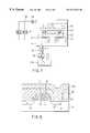
- FIG. 1is a schematic sectional view of a single-wafer processing LPCVD apparatus used in a first embodiment
- FIG. 2is a cross-sectional view of a semiconductor substrate having a MOS capacitor according to the present invention
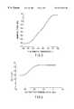
- FIG. 3is a characteristic graph showing the relationship between deposition temperature of a polysilicon film and film stress
- FIGS. 4A and 4Bshow that a semiconductor substrate is bent by a compression stress or tensile stress generated in a gate electrode (polysilicon film);
- FIGS. 5A and 5Bare conceptual diagram for explaining how a bent amount is calculated, FIG. 5A relates to the situation prior to the formation of a polysilicon film on the silicon substrate, and FIG. 5B relates to the situation after the formation of a polysilicon film on the silicon substrate.
- FIG. 6is a characteristic graph showing the relationship between the film stress of the polysilicon film and the total charge amount of a gate insulating film
- FIG. 7is a schematic sectional view of a single-wafer processing LPCVD apparatus used in a second embodiment
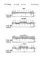
- FIG. 8is a cross sectional view of EEPROM according to a third embodiment
- FIGS. 9A and 9Bare cross sectional views showing manufacturing steps of a semiconductor substrate having a conventional MOS transistor.
- FIGS. 10A and 10Bare cross sectional views showing the manufacturing steps of a semiconductor substrate having a conventional MOS transistor.
- FIGS. 1 to 6a first embodiment will be explained.
- FIG. 1is a schematic sectional view of a single-wafer processing LPCVD (Low pressure CVD) apparatus.
- FIG. 2is a cross sectional view of a MOS capacitor formed on a semiconductor substrate.
- FIG. 3is a characteristic graph showing dependency of the film stress (MPa) of the polysilicon film on the semiconductor substrate upon deposition temperature.
- FIGS. 4A to 5 Bare conceptual diagram explaining the way of measuring a film stress.
- FIG. 6is a characteristics graph showing a total charge amount Qbd (C/cm 2 ) of the gate insulating film.
- the LPCVD apparatushas a reaction chamber 13 (hereinafter, referred to as “film formation chamber”).
- the film-formation chamber 13is equipped with a susceptor 15 on which a semiconductor wafer 16 is mounted.
- the inner space of the film formation chamber 13is heated by a plurality of infrared lamps 14 arranged around the chamber in close proximity thereto, during film formation time.
- a reactive gasis supplied from a pipe 10 to the inner space of the film formation chamber 13 while being controlled by a mass-flow controller 11 and a valve 12 .
- an exhaust gasis discharged by a pump 112 through a pipe 111 .
- the pump 112is controlled by a valve 18 and a conductance valve 19 while the pressure is monitored by a pressure gage 17 attached to the pipe 111 .
- an thermal oxidation film serving as a gate insulating film 122 and formed on a silicon semiconductor substrate 121is oxidized with O 2 , H 2 O, or HCl gas at a temperature of 800° C. to render the thickness at 8 nm.
- the semiconductor substrate 121semiconductor wafer 16
- the film-formation chamber 13 of the LPCVD apparatus shown in FIG. 1the film-formation chamber 13 of the LPCVD apparatus shown in FIG. 1 .
- a polysilicon film 123is formed on the semiconductor wafer 16 in a thickness of about 200 nm at a film-formation temperature of 680° C.
- the concentration of As in the polysilicon film 123is about 1 ⁇ 10 20 atoms/cm 3 .
- the polysilicon film 123is annealed for 30 minutes at 900° C. under an N 2 atmosphere in order to activate a dopant.
- a photoresist(not shown) is coated onto the polysilicon film 123 and photolithographically patterned.
- the polysilicon film 123is further subjected to dry etching in accordance with anisotropic etching such as RIE (Reactive Ion Etching) to form the gate electrode 123 a .
- RIEReactive Ion Etching
- the gate electrode 123 ais formed of polysilicon film 123 , but the material of the gate electrode according to the present invention is never limited to a polysilicon, as being explained later.
- source/drain regions 124are formed in the semiconductor substrate 121 . However, in the case of examining the electric characteristics of gate insulating film, the formation of source/drain regions 124 is omitted since they are unnecessary in the above examination.
- the gate electrode 123 amay also be formed of at least one of a metal silicide film and a high-melting point metal film.
- FIG. 3shows the relation between a deposit temperature of a polysilicon film (gate electrode) and a film stress.
- the longitudinal axisindicates a film stress (MPa) of the polysilicon film on the semiconductor substrate
- the lateral axisindicates the film formation temperature (° C.) of the polysilicon film.
- the polysilicon filmswere formed by deposition on the substrate in the same manner under the same conditions as in the aforementioned steps for manufacturing a capacitor, except the film formation temperature, that is, by varying the film formation temperature, and then annealing the polysilicon film, whereby obtaining various semiconductor wafers having capacitors of various electric characteristics. Thereafter, the stress of the polysilicon film alone was checked on the basis of warpage of the semiconductor wafer.
- the stress of the polysilicon film itselfwas measured as follows.
- compressive stress or tensile stressis generated in the polysilicon film, depending upon a deposition temperature of the polysilicon film.
- “upward warpage” bentis produced, as shown in FIG. 4 A.
- “downward warpage” bentis produced, as shown in FIG. 4 B.
- the “upward warpage” bentwill be expressed by a positive value, whereas the “downward warpage” bent by a negative value.
- FIGS. 5A and 5Bare conceptual views showing how to obtain a warpage amount, arithmetically.
- FIG. 5Ashows a state before the polysilicon film is deposited on a substrate.
- FIG. 5Bshows a state after the polysilicon film is deposited on the substrate.
- reference symbol tsdenotes a thickness of a substrate
- tris a thickness of the deposited film (polysilicon film)
- Dis a diameter of the portion at which warpage is measured (corresponding to the warpage)
- Xis a warpage amount ( ⁇ m).
- ⁇is a film stress
- Esis a Young's modulus of a substrate (semiconductor wafer)
- ⁇ sis a Poisson's ratio of the substrate.
- Equation IIEquation II is deduced.
- ⁇E s 6 ⁇ ( 1 - ⁇ s ) ⁇ ( t s ) 2 t r ⁇ 1 r ⁇ E s 6 ⁇ ( 1 - ⁇ s ) ⁇ ( t s ) 2 t r ⁇ 8 ⁇ X D 2 ( II )
- stress ⁇is obtained on the basis of the warpage amount X.
- a “upward warpage”is defined as a positive value
- a “downward warpage”a negative value
- a film stress in the case of “upward warpage”has a positive value
- a film stress in the case of a “downward warpage”has a negative value.
- the film stress of the polysilicon film aloneis defined as the difference in warpage amount before and after the polysilicon film is deposited, as being illustrated in FIGS. 5A and 5B.
- the warpage amountis measured by using Flexsus FLX-2418 (manufactured by KLA Tencor Corporation), as a measuring device.
- the film stressis as small as 50 MPa (absolute value) or less at a deposition temperature of 700° C. or more.
- a compressive stressis expressed, while a tensile stress reaches as large as ⁇ 300 MPa at near 620° C.
- the stress immediately after the polysilicon film is formedis 100 MPa or less. This value does not so significantly differ from that obtained after the annealing.
- FIG. 6shows the results of a total charge amount Qbd of the gate insulating film measured under an electric field of 12 MV/cm, in the MOS capacitor thus formed on the semiconductor substrate.
- the total charge amount Qbdis defined as the total amount of electric charge passing through the capacitor per unit area when a plurality of capacitors formed in the same plane of the semiconductor wafer are measured and a failure rate thereof reaches 50%.
- the total amount of the electric charge Qbdis about 15 C/cm 2 .
- the total charge amount Qbdis as large as 25 C/cm 2 or more.
- the total charge amount of the gate insulating film 122is 25 C/cm 2 or more when the polysilicon film forming gate electrode 123 a is formed at a film formation temperature of 640° C. or more, preferably 650° C. or more.
- the atmosphere pressure in depositing a polysilicon film serving as a gate electrodemay be in a range of 20 to 200 Torr.
- a single-wafer processing LPCVD apparatusis used.
- a batch processing LPCVD apparatus usually employed in manufacturing a semiconductor devicemay be used.
- the polysilicon film serving as the gate electrodewas formed, at a temperature from 500° C. to 630° C. and a pressure from 0.3 Torr to 1 Torr while SiH 4 gas is supplied at a flow rate from 200 sccm to 1000 sccm.
- the polysilicon film formed at a temperature of 580° C. or morewas crystallized.
- the film stresswas ⁇ 300 MPa or less (300 MPa or less in terms of absolute value).
- the results for the MOS capacitor manufactured by the batch processing LPCVD apparatuswere the same as those of the MOS capacitor manufactured by the single-wafer processing LPCVD apparatus. That is, the total charge amount Qbd causing dielectric breakdown of the gate insulating film was about 15 C/cm 2 . Furthermore, the silicon film deposited at a film formation temperature of 580° C. or less is in an amorphous state and has a compressive film stress of about ⁇ 300 MPa. The amorphous film is crystallized into a polysilicon film in the annealing step performed later. The film stress of the polysilicon film greatly increases to a tensile stress of about 300 MPa in absolute value.
- the total charge amount of the gate insulating filmcomes to about 15/cm 2 .
- the MOS capacitor manufactured by the batch processing LPCVD apparatussatisfies the same relationship between the total charge amount Qbd of the gate insulating film and the film stress of the gate electrode shown in FIGS. 3 and 6.
- the gate insulating film of 8 nm thickis used in this embodiment.
- the total charge amount of the gate insulating filmvaries, accordingly.
- the total charge amount Qbdreduces, whereas when the film thickness increases, the total charge amount Qbd increases.
- the relationship between the film stress and the total charge amount of the gate insulating filmis unchanged. That is, when the film stress of the gate electrode increases, the total charge amount of the gate insulating film decreases.
- the total charge amount Qbdis about twice as large as that obtained at the film stress of 300 MPa.
- the gate electrodeis formed of another substance such as a metal including tungsten (W)
- the effect of the film stress upon the total charge amount Qbd of the gate insulating filmis similar and thus, the same phenomenon is observed.
- the metal electrodewhen used, it is effective to set the film stress of the gate electrode at 200 MPa or less in terms of absolute value, in order to improve the total charge amount Qbd of the gate insulating film, in other word, to improve reliability thereof.
- a single-wafer processing LPCVD apparatusis used.
- the single-wafer processing LPCVD apparatusis heated at high temperatures, the formed film is sometimes degraded in uniformity in thickness.
- the semiconductor waferis rotated in the apparatus.
- FIG. 7is a schematic sectional view of the single-wafer processing LPCVD apparatus.
- the LPCVD apparatushas a reaction chamber (film formation chamber) 21 .
- a wafer holder 22is provided for mounting a semiconductor wafer 24 thereon.
- the wafer holder 22is designed so as to rotate at a predetermined rotation number to rotate the semiconductor wafer 24 .
- the film formation chamber 21has a heater 23 therein for heating an inner space during film formation time.
- a reactive gasis supplied to the inner space of the film formation chamber 21 from a pipe 20 while being controlled by a mass-flow controller 27 and a valve 26 .
- an exhaust gasis discharged through a pipe 211 by a pump 210 .
- the pump 210is controlled by a valve 28 and a conductance valve 29 .
- a gas flow 25 of the reactive gas supplied through the pipe 20enters from an upper portion of the film formation chamber 21 , passes through slits and is supplied uniformly over a surface of the semiconductor wafer 24 in rotation. After completion of a reaction, the gas flow 25 is discharged from the pipe 211 .
- a semiconductor waferwas placed in the single-wafer processing LPCVD apparatus thus constructed and a reactive gas flow was supplied uniformly over the surface of the semiconductor wafer while the semiconductor wafer was rotated at a high speed.
- a polysilicon filmwas formed on a semiconductor wafer.
- the polysilicon filmwas formed by supplying SiH 4 at a flow rate of 1 SLM, AsH 3 at a flow rate of 3 sccm under a pressure of 50 Torr, and N 2 at a flow rate of 30 SLM, while the semiconductor wafer was rotated at a rotation number of 3000 rpm, the resultant polysilicon film was excellent in uniformity ( ⁇ 3% or less) in thickness within the semiconductor wafer surface plane at the film formation temperature ranging from 600° C.
- the film stress of the polysilicon filmsatisfied the same relationship between the film formation temperature and the film stress shown in FIG. 3 .
- MOS capacitorswere formed on a semiconductor substrate and a total charge amount Qbd determining dielectric breakdown of the gate insulating films of the capacitors was examined and measured. The results are the same as shown in FIG. 6 . That is, according to the second embodiment, it is possible to provide a semiconductor device having a highly liable gate insulating film, with keeping a very preferable uniformity in film thickness.
- FIG. 8a third embodiment will be explained.
- FIG. 8is a cross sectional view of an EEPROM memory cell according to the third embodiment of the invention.
- the EEPROMis a non-volatile electrically erasable and programmable memory, and mostly used in a new fields including a logic array capable of programming data memory and logic in a logic circuit, e.g., a micro computer, data memories, and program memories of IC cards.
- a p-type semiconductor substrate 31is used as the semiconductor substrate.
- the surface of the semiconductor substrate 31is oxidized with O 2 , H 2 O, or HCl gas at a temperature of 800° C. to form a thermal oxide film 34 of 8 nm thick serving as a gate insulating film.
- a polysilicon film 35 constituting a floating gateis formed on the semiconductor wafer of about 200 nm thick at a film formation temperature of 680° C. while SiH 4 gas is supplied at a flow rate of 1 SLM and AsH 3 gas at 1 sccm under a pressure of 5 Torr.
- the film stress of polysilicon film 35can be suppressed less than about 200 MPa in its absolute value by forming polysilicon film in the same manner as above the first embodiment or the second embodiment.
- the polysilicon film 35 constituting a floating gatecan have a total charge amount Qbd twice as large as a conventional one, so that a semiconductor device having a highly liable floating gate can be provided.
- arsenicis introduced into the polysilicon film 35 in an amount of about 1 ⁇ 10 20 atoms/cm 3 . Thereafter, the polysilicon film 35 is annealed at 900° C. for 30 minutes under a N 2 atmosphere in order to activate a dopant.
- a photoresist(not shown) is coated onto the polysilicon film 35 and photolithographically patterned.
- the resultant polysilicon film 35is etched by a RIE method to form a floating gate 35 of polysilicon.
- an interlayer insulating film (SiO 2 ) film 36is formed on the semiconductor wafer by a CVD method so as to cover the floating gate 35 .
- a polysilicon film 37is formed on the semiconductor wafer of about 200 nm thick, for example, in the LPCVD apparatus shown in FIG. 1, in the same conditions as in the formation time of the floating gate 35 .
- Arsenic (As)is introduced into the polysilicon film 37 in an amount of about 1 ⁇ 10 20 atoms/cm 3 .
- the polysilicon film 37is annealed at 900° C. under a N 2 atmosphere in order to activate a dopant.
- a photoresist(not shown) is coated onto the polysilicon film 37 and photolithographically patterned.
- the polysilicon film 37is etched by RIE to form a control gate 37 of polysilicon.
- the single-wafer processing LPCVD apparatus shown in FIG. 1is used in this case, however, the polysilicon film forming the gate electrode may be formed in the single-wafer processing LPCVD apparatus shown in FIG. 7 .
- n-type impurity ionssuch as boron are doped in the semiconductor substrate 31 by using the control gate 37 as a mask and thermally diffused to form an n + source region 32 and an n + drain region 33 .
- an insulating film (SiO 2 ) 38is deposited by the CVD method on the semiconductor substrate 31 so as to cover the control gate 37 .
- the surface of the insulating film 38is planarized by a CMP (Chemical Mechanical Polishing) method.
- a photoresist(not shown) is coated onto the insulating film 38 and photolithographically pattered.
- the resultant insulating film 38is etched by RIE etc. to form a contact hole 38 through which the drain region 33 is exposed.
- an aluminium film 310is deposited by a sputtering method on the insulating film 38 and within the contact hole 39 , and photolithographically patterned to form a metal wiring 310 .
- the Qbd valueis significant since it determines how many times the device can be programmed. Therefore, it is necessary to increase the total charge amount Qbd in order to improve the performance of the device.
- the EEPROMin which the total amount Qbd of the electric charge passing through the gate insulating film directly influences upon characteristics of a device, the number of times the device can be programmed or rewritten is greatly improved by the present invention. Since the film stress of the gate electrode according to the present invention is suppressed to 200 MPa or less in terms of absolute value, the total charge amount Qbd of the gate insulating film increases nearly double.
Landscapes
- Chemical & Material Sciences (AREA)
- Engineering & Computer Science (AREA)
- General Chemical & Material Sciences (AREA)
- Chemical Kinetics & Catalysis (AREA)
- Manufacturing & Machinery (AREA)
- Computer Hardware Design (AREA)
- Microelectronics & Electronic Packaging (AREA)
- Power Engineering (AREA)
- Condensed Matter Physics & Semiconductors (AREA)
- Inorganic Chemistry (AREA)
- Physics & Mathematics (AREA)
- General Physics & Mathematics (AREA)
- Materials Engineering (AREA)
- Mechanical Engineering (AREA)
- Metallurgy (AREA)
- Organic Chemistry (AREA)
- Insulated Gate Type Field-Effect Transistor (AREA)
- Semiconductor Memories (AREA)
- Formation Of Insulating Films (AREA)
- Non-Volatile Memory (AREA)
- Electrodes Of Semiconductors (AREA)
Abstract
Description
The present invention relates to a semiconductor device constituted of an integrated circuit having a MOS transistor formed therein, and more particularly, to a method of forming a gate electrode for improving reliability of a gate insulating film of the MOS transistor.
Now, we will explain steps of manufacturing the MOS transistor which serves as a constitutional element of an integrated circuit formed on a conventional semiconductor substrate, by taking an NMOS transistor having an LDD (lightly doped drain) structure, as an example. First, anelement isolating region 2 is formed on a surface region of a p-typesilicon semiconductor substrate 1 by a LOCOS method or the like. A gate insulating film (SiO2)3 is formed on an element region surrounded by theelement isolating region 2. Then, boron ions are injected (channel ion injection) over an entire main surface of thesemiconductor substrate 1 to control a threshold voltage (FIG.9A). Subsequently, a polysilicon film is deposited over the entire main surface of thesemiconductor substrate 1 and patterned to form a gate electrode4 of polysilicon (PolySi) on the gateinsulating film 3 in the element region. Thereafter, P (phosphorus) ions are injected in a low amount to form an n− source/drain region 5 for mitigating a high electric field (FIG.9B).
Next, a silicon oxide film (SiO2)6 is deposited on thesemiconductor substrate 1 by a CVD (Chemical Vapor Deposition) method or the like so as to cover the gate electrode4 (FIG.10A). Subsequently, thesilicon oxide film 6 is anisotoropically etched to form a side wall insulating film7 on a side wall of the gate electrode4. Thereafter, n-type impurity ions such as arsenic (As) ions are doped in a high amount to form an n+ source/drain region8 (FIG.10B).
As described above, in the MOS transistor, a polysilicon film doped with phosphorus, arsenic, or boron is generally used as the gate electrode. The polysilicon film is deposited by an LPCVD method at a reaction-chamber ambient temperature of about 600° C. The polysilicon film deposited under the aforementioned conditions has a film stressfilm stress of 300 MPa or more despite the presence or absence of a dopant. Such a high stress of the gate electrode is applied to a gate insulating film (in this prior art, the film may be composed of a silicon oxide film, hereinafter simply called “gate insulating film”, for the simplicity of explanation) whereby the high stress affects reliability of the gate insulating film or gate insulating film formed under the gate electrode. To explain more specifically, when the stress is applied to the gate insulating film, the bonding between silicon and oxygen constituting the gate insulating film is distorted. As a result, the bonding tends to be easily broken, readily inducing dielectric breakdown of the gate insulating film.
When intrinsic dielectric breakdown of the insulating film takes place, the total amount Qbd of electric charge passing through the insulating film is up to about 15 C/cm2under application of an electric field of 12 MV/cm to the insulating film, assuming that the thickness of the insulating film is about 10 nm. The total charge amount Qbd is a value on the basis of which the reliability of a transistor is determined. Therefore, the Qbd desirably has a large value. Particularly, in non-volatile storage device, such as EEPROM (Electrically Erasable Programmable Read Only memory) in which data is written into a memory cell by using a tunnel current, how many times the device can be programmed is restricted by the total charge amount Qbd. Therefore, it is necessary to increase the total charge amount Qbd in order to improve performance of the device.
The present invention was made in view of the aforementioned circumstances. The present invention provides a semiconductor device and a method of manufacturing the same, improved in reliability of a gate insulating film and increased in its total charge amount Qbd by suppressing a film stress of a gate electrode formed of a polysilicon film, to a low value.
Since the film stress of a gate electrode is closely related with a film formation temperature, it is possible to reduce the film stress lower than in the conventional case, by forming a film at as a high temperature as 640° C. or more, preferably 650° C. or more. With a decrease in the film stress of the gate electrode at this time, the total charge amount Qbd of a gate insulating film underlying the gate electrode increases, with the result that reliability not only of the gate insulating film but also a semiconductor device including the gate insulating film is improved.
More specifically, the semiconductor device of the present invention comprises
a semiconductor substrate;
source/drain regions formed on the semiconductor substrate;
a gate insulating film formed between the source/drain regions on the semiconductor substrate; and
a gate electrode formed on the gate insulating film,
in which
a film stress of the gate electrode is 200 MPa or less in terms of absolute value.
The gate electrode may be a polysilicon film and may be in contact with the gate insulating film.
A metal silicide film or a high-melting point metal film may be formed on the polysilicon film. In other words, the gate electrode may be formed of the polysilicon film and the metal silicide film or the high melting point metal film. Furthermore, the high melting point metal film is formed on the metal silicide film, and therefore, the gate electrode may be formed of the polysilicon film, the metal silicide film, and the high melting point metal film.
A MOS transistor having the source/drain regions, the gate insulating film, and the gate electrode, may be adopted in a non-volatile semiconductor storage device such as an EEPROM. When the MOS transistor according to the invention is used in an EEPROM, the programmable number can be increased since a total charge amount Qbd of electric charge passing through the gate insulating film serving as a floating gate has a direct effect upon characteristics of a device.
According to the present invention, there is provided a method of manufacturing a semiconductor device, according to the present invention comprises the steps of:
forming source/drain regions in a semiconductor substrate;
forming a gate insulating film between the source/drain regions on the semiconductor substrate; and
forming a gate electrode including a polysilicon film on the gate insulating film and having a film stress of 200 MPa or less;
in which
the polysilicon film is formed by depositing polysilicon on the gate insulating film by a CVD method at a temperature of 640° C. or more. Preferably, the temperature at which a gate insulating film is formed may be 650° C. or more, in order to stably provide a gate electrode whose film stress is 200 MPa or less.
The polysilicon film may be formed while the semiconductor substrate is rotated at a high speed. In this manner, it is possible to form a uniform film on a semiconductor substrate.
Additional objects and advantages of the invention will be set forth in the description which follows, and in part will be obvious from the description, or may be learned by practice of the invention. The objects and advantages of the invention may be realized and obtained by means of the instrumentalities and combinations particularly pointed out hereinafter.
The accompanying drawings, which are incorporated in and constitute a part of the specification, illustrate presently preferred embodiments of the invention, and together with the general description given above and the detailed description of the preferred embodiments given below, serve to explain the principles of the invention.
FIG. 1 is a schematic sectional view of a single-wafer processing LPCVD apparatus used in a first embodiment;
FIG. 2 is a cross-sectional view of a semiconductor substrate having a MOS capacitor according to the present invention;
FIG. 3 is a characteristic graph showing the relationship between deposition temperature of a polysilicon film and film stress;
FIGS. 4A and 4B show that a semiconductor substrate is bent by a compression stress or tensile stress generated in a gate electrode (polysilicon film);
FIGS. 5A and 5B are conceptual diagram for explaining how a bent amount is calculated, FIG. 5A relates to the situation prior to the formation of a polysilicon film on the silicon substrate, and FIG. 5B relates to the situation after the formation of a polysilicon film on the silicon substrate.
FIG. 6 is a characteristic graph showing the relationship between the film stress of the polysilicon film and the total charge amount of a gate insulating film;
FIG. 7 is a schematic sectional view of a single-wafer processing LPCVD apparatus used in a second embodiment;
FIG. 8 is a cross sectional view of EEPROM according to a third embodiment;
FIGS. 9A and 9B are cross sectional views showing manufacturing steps of a semiconductor substrate having a conventional MOS transistor; and
FIGS. 10A and 10B are cross sectional views showing the manufacturing steps of a semiconductor substrate having a conventional MOS transistor.
Now, embodiments of the present invention will be explained with reference to the accompanying drawings.
First, referring to FIGS. 1 to6, a first embodiment will be explained.
FIG. 1 is a schematic sectional view of a single-wafer processing LPCVD (Low pressure CVD) apparatus. FIG. 2 is a cross sectional view of a MOS capacitor formed on a semiconductor substrate. FIG. 3 is a characteristic graph showing dependency of the film stress (MPa) of the polysilicon film on the semiconductor substrate upon deposition temperature. FIGS. 4A to5B are conceptual diagram explaining the way of measuring a film stress. FIG. 6 is a characteristics graph showing a total charge amount Qbd (C/cm2) of the gate insulating film.
As shown in FIG. 1, the LPCVD apparatus has a reaction chamber13 (hereinafter, referred to as “film formation chamber”). The film-formation chamber 13 is equipped with asusceptor 15 on which asemiconductor wafer 16 is mounted. The inner space of thefilm formation chamber 13 is heated by a plurality ofinfrared lamps 14 arranged around the chamber in close proximity thereto, during film formation time. A reactive gas is supplied from apipe 10 to the inner space of thefilm formation chamber 13 while being controlled by a mass-flow controller 11 and avalve 12. After completion of a reaction, an exhaust gas is discharged by apump 112 through apipe 111. Thepump 112 is controlled by avalve 18 and aconductance valve 19 while the pressure is monitored by apressure gage 17 attached to thepipe 111.
As shown in FIG. 2, an thermal oxidation film serving as agate insulating film 122 and formed on asilicon semiconductor substrate 121 is oxidized with O2, H2O, or HCl gas at a temperature of 800° C. to render the thickness at 8 nm. Thereafter, the semiconductor substrate121 (semiconductor wafer16) is placed in the film-formation chamber 13 of the LPCVD apparatus shown in FIG.1. Then, apolysilicon film 123 is formed on thesemiconductor wafer 16 in a thickness of about 200 nm at a film-formation temperature of 680° C. and a pressure of 5 Torr while SiH4gas is supplied at a flow rate of 1 SLM and AsH3gas at a flow rate of 1 sccm. At this time, the concentration of As in thepolysilicon film 123 is about 1×10²⁰atoms/cm3. Thereafter, thepolysilicon film 123 is annealed for 30 minutes at 900° C. under an N2atmosphere in order to activate a dopant. Thereafter, a photoresist (not shown) is coated onto thepolysilicon film 123 and photolithographically patterned. Thepolysilicon film 123 is further subjected to dry etching in accordance with anisotropic etching such as RIE (Reactive Ion Etching) to form thegate electrode 123a. Finally, a capacitor of a layered structure: a gate electrode-gate insulating film-a semiconductor substrate, was formed. Then, electric characteristics of the gate insulating film were examined by using the capacitor. In this embodiment, thegate electrode 123ais formed ofpolysilicon film 123, but the material of the gate electrode according to the present invention is never limited to a polysilicon, as being explained later. In the case that a device according to the present invention is actually fabricated, source/drain regions 124 are formed in thesemiconductor substrate 121. However, in the case of examining the electric characteristics of gate insulating film, the formation of source/drain regions 124 is omitted since they are unnecessary in the above examination.
Thegate electrode 123amay also be formed of at least one of a metal silicide film and a high-melting point metal film.
FIG. 3 shows the relation between a deposit temperature of a polysilicon film (gate electrode) and a film stress. In FIG. 3, the longitudinal axis indicates a film stress (MPa) of the polysilicon film on the semiconductor substrate, and the lateral axis indicates the film formation temperature (° C.) of the polysilicon film. The polysilicon films were formed by deposition on the substrate in the same manner under the same conditions as in the aforementioned steps for manufacturing a capacitor, except the film formation temperature, that is, by varying the film formation temperature, and then annealing the polysilicon film, whereby obtaining various semiconductor wafers having capacitors of various electric characteristics. Thereafter, the stress of the polysilicon film alone was checked on the basis of warpage of the semiconductor wafer.
The stress of the polysilicon film itself was measured as follows.
Generally, compressive stress or tensile stress is generated in the polysilicon film, depending upon a deposition temperature of the polysilicon film. When the compressive stress is generated, “upward warpage” bent is produced, as shown in FIG.4A. On the other hand, when the tensile stress is generated, “downward warpage” bent is produced, as shown in FIG.4B. Hereinafter, the “upward warpage” bent will be expressed by a positive value, whereas the “downward warpage” bent by a negative value.
FIGS. 5A and 5B are conceptual views showing how to obtain a warpage amount, arithmetically. FIG. 5A shows a state before the polysilicon film is deposited on a substrate. FIG. 5B shows a state after the polysilicon film is deposited on the substrate. In the figures, reference symbol ts denotes a thickness of a substrate, tr is a thickness of the deposited film (polysilicon film), D is a diameter of the portion at which warpage is measured (corresponding to the warpage), and X is a warpage amount (μm).

where σ is a film stress, Es is a Young's modulus of a substrate (semiconductor wafer), and γsis a Poisson's ratio of the substrate.


Accordingly, stress σ is obtained on the basis of the warpage amount X. As mentioned before, since a “upward warpage” is defined as a positive value, and a “downward warpage” a negative value, a film stress in the case of “upward warpage” has a positive value, while a film stress in the case of a “downward warpage” has a negative value.
The film stress of the polysilicon film alone is defined as the difference in warpage amount before and after the polysilicon film is deposited, as being illustrated in FIGS. 5A and 5B. The warpage amount is measured by using Flexsus FLX-2418 (manufactured by KLA Tencor Corporation), as a measuring device.
Referring again to FIG. 3, it has been found that the film stress is as small as 50 MPa (absolute value) or less at a deposition temperature of 700° C. or more. As the film formation temperature decreases from 700° C., a compressive stress is expressed, while a tensile stress reaches as large as −300 MPa at near 620° C. On the other hand, the stress immediately after the polysilicon film is formed, is 100 MPa or less. This value does not so significantly differ from that obtained after the annealing.
FIG. 6 shows the results of a total charge amount Qbd of the gate insulating film measured under an electric field of 12 MV/cm, in the MOS capacitor thus formed on the semiconductor substrate. Note that the total charge amount Qbd is defined as the total amount of electric charge passing through the capacitor per unit area when a plurality of capacitors formed in the same plane of the semiconductor wafer are measured and a failure rate thereof reaches 50%.
In the case where the film stress is smaller than −300 MPa, the total amount of the electric charge Qbd is about 15 C/cm2. However, in the case where the film stress ranges from −200 MPa to about +30 MPa, the total charge amount Qbd is as large as 25 C/cm2or more. This means that the total charge amount of thegate insulating film 122 is 25 C/cm2or more when the polysilicon film forminggate electrode 123ais formed at a film formation temperature of 640° C. or more, preferably 650° C. or more. In addition, in a preferable embodiment, the atmosphere pressure in depositing a polysilicon film serving as a gate electrode may be in a range of 20 to 200 Torr.
In this embodiment, a single-wafer processing LPCVD apparatus is used. In the present invention, however, a batch processing LPCVD apparatus usually employed in manufacturing a semiconductor device, may be used.
By using the batch processing LPCVD apparatus, the polysilicon film serving as the gate electrode was formed, at a temperature from 500° C. to 630° C. and a pressure from 0.3 Torr to 1 Torr while SiH4gas is supplied at a flow rate from 200 sccm to 1000 sccm. As a result, the polysilicon film formed at a temperature of 580° C. or more was crystallized. At this time, the film stress was −300 MPa or less (300 MPa or less in terms of absolute value).
The results for the MOS capacitor manufactured by the batch processing LPCVD apparatus were the same as those of the MOS capacitor manufactured by the single-wafer processing LPCVD apparatus. That is, the total charge amount Qbd causing dielectric breakdown of the gate insulating film was about 15 C/cm2. Furthermore, the silicon film deposited at a film formation temperature of 580° C. or less is in an amorphous state and has a compressive film stress of about −300 MPa. The amorphous film is crystallized into a polysilicon film in the annealing step performed later. The film stress of the polysilicon film greatly increases to a tensile stress of about 300 MPa in absolute value. When such a polysilicon film is used, the total charge amount of the gate insulating film comes to about 15/cm2. The MOS capacitor manufactured by the batch processing LPCVD apparatus satisfies the same relationship between the total charge amount Qbd of the gate insulating film and the film stress of the gate electrode shown in FIGS. 3 and 6.
The same results as in the aforementioned embodiment are given in the case where MOS capacitor having a polysilicon film doped with phosphorus (P) or boron (B) is used in place of the film doped with arsenic (AS). Furthermore, even if the concentration of the dopant is varied, the same results are obtained. Thus, it has been found that the film stress of a gate electrode is determined mainly by its film formation temperature, regardless of dopant materials or dopant concentration.
The gate insulating film of 8 nm thick is used in this embodiment. When the film thickness of the oxide film is changed, the total charge amount of the gate insulating film varies, accordingly. When the film thickness of the gate insulating film decreases, the total charge amount Qbd reduces, whereas when the film thickness increases, the total charge amount Qbd increases. However, the relationship between the film stress and the total charge amount of the gate insulating film is unchanged. That is, when the film stress of the gate electrode increases, the total charge amount of the gate insulating film decreases. To be more specific, when the film stress is 200 MPa or less, the total charge amount Qbd is about twice as large as that obtained at the film stress of 300 MPa.
In the case where the gate electrode is formed of another substance such as a metal including tungsten (W), the effect of the film stress upon the total charge amount Qbd of the gate insulating film is similar and thus, the same phenomenon is observed. Hence, when the metal electrode is used, it is effective to set the film stress of the gate electrode at 200 MPa or less in terms of absolute value, in order to improve the total charge amount Qbd of the gate insulating film, in other word, to improve reliability thereof.
Referring to FIG. 7, a second embodiment will be explained.
In the first embodiment, a single-wafer processing LPCVD apparatus is used. When the single-wafer processing LPCVD apparatus is heated at high temperatures, the formed film is sometimes degraded in uniformity in thickness. To maintain the uniformity of film thickness, the semiconductor wafer is rotated in the apparatus.
FIG. 7 is a schematic sectional view of the single-wafer processing LPCVD apparatus. As shown in the figure, the LPCVD apparatus has a reaction chamber (film formation chamber)21. In thefilm formation chamber 21, awafer holder 22 is provided for mounting asemiconductor wafer 24 thereon. Thewafer holder 22 is designed so as to rotate at a predetermined rotation number to rotate thesemiconductor wafer 24. Thefilm formation chamber 21 has aheater 23 therein for heating an inner space during film formation time. A reactive gas is supplied to the inner space of thefilm formation chamber 21 from apipe 20 while being controlled by a mass-flow controller 27 and avalve 26. After completion of a reaction, an exhaust gas is discharged through apipe 211 by apump 210. Thepump 210 is controlled by avalve 28 and aconductance valve 29.
Agas flow 25 of the reactive gas supplied through thepipe 20 enters from an upper portion of thefilm formation chamber 21, passes through slits and is supplied uniformly over a surface of thesemiconductor wafer 24 in rotation. After completion of a reaction, thegas flow 25 is discharged from thepipe 211.
A semiconductor wafer was placed in the single-wafer processing LPCVD apparatus thus constructed and a reactive gas flow was supplied uniformly over the surface of the semiconductor wafer while the semiconductor wafer was rotated at a high speed. In this manner, a polysilicon film was formed on a semiconductor wafer. When the polysilicon film was formed by supplying SiH4at a flow rate of 1 SLM, AsH3at a flow rate of 3 sccm under a pressure of 50 Torr, and N2at a flow rate of 30 SLM, while the semiconductor wafer was rotated at a rotation number of 3000 rpm, the resultant polysilicon film was excellent in uniformity (±3% or less) in thickness within the semiconductor wafer surface plane at the film formation temperature ranging from 600° C. to 900° C. In this case, the film stress of the polysilicon film satisfied the same relationship between the film formation temperature and the film stress shown in FIG.3. Then, MOS capacitors were formed on a semiconductor substrate and a total charge amount Qbd determining dielectric breakdown of the gate insulating films of the capacitors was examined and measured. The results are the same as shown in FIG.6. That is, according to the second embodiment, it is possible to provide a semiconductor device having a highly liable gate insulating film, with keeping a very preferable uniformity in film thickness.
Now, referring to FIG. 8, a third embodiment will be explained.
FIG. 8 is a cross sectional view of an EEPROM memory cell according to the third embodiment of the invention. The EEPROM is a non-volatile electrically erasable and programmable memory, and mostly used in a new fields including a logic array capable of programming data memory and logic in a logic circuit, e.g., a micro computer, data memories, and program memories of IC cards.
As the semiconductor substrate, for example, a p-type semiconductor substrate 31 is used. The surface of thesemiconductor substrate 31 is oxidized with O2, H2O, or HCl gas at a temperature of 800° C. to form athermal oxide film 34 of 8 nm thick serving as a gate insulating film.
Thereafter, thesemiconductor substrate 31 is placed as a semiconductor wafer in the film formation chamber of the LPCVD apparatus shown in FIG. 1. Apolysilicon film 35 constituting a floating gate is formed on the semiconductor wafer of about 200 nm thick at a film formation temperature of 680° C. while SiH4gas is supplied at a flow rate of 1 SLM and AsH3gas at 1 sccm under a pressure of 5 Torr. The film stress ofpolysilicon film 35 can be suppressed less than about 200 MPa in its absolute value by forming polysilicon film in the same manner as above the first embodiment or the second embodiment. As a result thepolysilicon film 35 constituting a floating gate can have a total charge amount Qbd twice as large as a conventional one, so that a semiconductor device having a highly liable floating gate can be provided.
At this time, arsenic (AS) is introduced into thepolysilicon film 35 in an amount of about 1×10²⁰atoms/cm3. Thereafter, thepolysilicon film 35 is annealed at 900° C. for 30 minutes under a N2atmosphere in order to activate a dopant.
Subsequently, a photoresist (not shown) is coated onto thepolysilicon film 35 and photolithographically patterned. Theresultant polysilicon film 35 is etched by a RIE method to form a floatinggate 35 of polysilicon. Then, an interlayer insulating film (SiO2)film 36 is formed on the semiconductor wafer by a CVD method so as to cover the floatinggate 35. Subsequently, apolysilicon film 37 is formed on the semiconductor wafer of about 200 nm thick, for example, in the LPCVD apparatus shown in FIG. 1, in the same conditions as in the formation time of the floatinggate 35. At this time, Arsenic (As) is introduced into thepolysilicon film 37 in an amount of about 1×10²⁰atoms/cm3. Thereafter, thepolysilicon film 37 is annealed at 900° C. under a N2atmosphere in order to activate a dopant. Thereafter, a photoresist (not shown) is coated onto thepolysilicon film 37 and photolithographically patterned. Thepolysilicon film 37 is etched by RIE to form acontrol gate 37 of polysilicon.
Note that the single-wafer processing LPCVD apparatus shown in FIG. 1 is used in this case, however, the polysilicon film forming the gate electrode may be formed in the single-wafer processing LPCVD apparatus shown in FIG.7.
Then, n-type impurity ions such as boron are doped in thesemiconductor substrate 31 by using thecontrol gate 37 as a mask and thermally diffused to form an n+ source region32 and an n+ drain region33. Then, an insulating film (SiO2)38 is deposited by the CVD method on thesemiconductor substrate 31 so as to cover thecontrol gate 37. The surface of the insulatingfilm 38 is planarized by a CMP (Chemical Mechanical Polishing) method. Then, a photoresist (not shown) is coated onto the insulatingfilm 38 and photolithographically pattered. The resultant insulatingfilm 38 is etched by RIE etc. to form acontact hole 38 through which thedrain region 33 is exposed. Subsequently, analuminium film 310 is deposited by a sputtering method on the insulatingfilm 38 and within thecontact hole 39, and photolithographically patterned to form ametal wiring 310.
As for the device such as EEPROM for writing data into a memory cell by using a tunnel current, the Qbd value is significant since it determines how many times the device can be programmed. Therefore, it is necessary to increase the total charge amount Qbd in order to improve the performance of the device. In the EEPROM in which the total amount Qbd of the electric charge passing through the gate insulating film directly influences upon characteristics of a device, the number of times the device can be programmed or rewritten is greatly improved by the present invention. Since the film stress of the gate electrode according to the present invention is suppressed to 200 MPa or less in terms of absolute value, the total charge amount Qbd of the gate insulating film increases nearly double. As a result, the life spans of transistors and LSI products having the MOS structure increase double, increasing reliability of the device. This feature is particularly useful in EEPROM in which the total charge amount Qbd directly influences upon characteristics of a device, since the number of times the device can be programmed or rewritten increases approximately double.
Additional advantages and modifications will readily occur to those skilled in the art. Therefore, the invention in its broader aspects is not limited to the specific details and representative embodiments shown and described herein. Accordingly, various modifications may be made without departing from the spirit or scope of the general inventive concept as defined by the appended claims and their equivalents.
Claims (23)
1. A semiconductor device comprising:
a semiconductor substrate;
source/drain regions formed in a surface of the substrate;
a gate insulating film disposed on a surface of the substrate between the source/drain regions; and
a gate electrode disposed on the gate insulating film, the gate electrode being set to have a film stress of 200 MPa or less in terms of absolute value, such that a total charge amount is 25 C/cm2or more, the total charge amount being an amount of electric charge passing through the gate insulating film when intrinsic dielectric breakdown of the gate insulating film takes place.
2. A device according toclaim 1 , wherein the gate electrode comprises a polysilicon film doped with an impurity.
3. A device according toclaim 2 , wherein the gate electrode consists essentially of the polysilicon film.
4. A device according toclaim 2 , wherein the film stress is a compressive stress.
5. A device according toclaim 2 , wherein the polysilicon film is a product formed by means of CVD process performed at a film formation temperature of 640° C. or more.
6. A device according toclaim 5 , wherein the film formation temperature is 650° C. or more.
7. A device according toclaim 5 , wherein the semiconductor substrate is rotated at a rotationally speed of 3000 rpm or more during the CVD process.
8. A device according toclaim 1 , wherein the gate insulating film comprises a silicon oxide film.
9. A device according toclaim 8 , wherein the gate insulating film consists essentially of the silicon oxide film.
10. A device according toclaim 9 , wherein the gate insulating film has a property such that the total charge amount is 25 C/cm2or more where the gate insulating film has a thickness of 8 nm and is supplied with an electric field of 12 MV/cm.
11. A non-volatile semiconductor memory device comprising:
a semiconductor substrate;
source/drain regions formed in a surface of the substrate;
a first gate insulating film disposed on a surface of the substrate between the source/drain regions;
a floating gate electrode disposed on the first gate insulating film, the floating gate electrode being set to have a film stress of 200 MPa or less in terms of absolute value, such that a total charge amount is 25 C/cm2or more, the total charge amount being an amount of electric charge passing through the fist gate insulating film when intrinsic dielectric breakdown of the first gate insulating film takes place;
a second gate insulating film disposed on the floating gate electrode; and a control gate electrode disposed on the gate insulating film.
12. A device according toclaim 11 , wherein the floating gate electrode comprises a polysilicon film doped with an impurity.
13. A device according toclaim 12 , wherein the floating gate electrode consists essentially of the polysilicon film.
14. A device according toclaim 12 , wherein the film stress is a compressive stress.
15. A device according toclaim 12 , wherein the polysilicon film is a product formed by means of CVD process performed at a film formation temperature of 640° C. or more.
16. A device according toclaim 15 , wherein the film formation temperature is 650° C. or more.
17. A device according toclaim 15 , wherein the semiconductor substrate is rotated at a rotational speed of 3000 rpm or more during the CVD process.
18. A device according toclaim 11 , wherein the first gate insulating film comprises a silicon oxide film.
19. A device according toclaim 18 , wherein the first gate insulating film consists essentially of the silicon oxide film.
20. A device according toclaim 19 , wherein the first gate insulating film has a property such that the total charge amount is 25 C/cm2or more where the first gate insulating film has a thickness of 8 nm and is supplied with an electric filed of 12 MV/cm.
21. A semiconductor device comprising:
a semiconductor substrate;
source/drain regions formed in a surface of the substrate;
a gate insulating film disposed on a surface of the substrate between the source/drain regions; and
a gate electrode disposed on the gate insulating film, the gate electrode being set to have a film stress of 200 MPa or less in terms of absolute value, in order to increase a total charge amount of electric charge passing through the gate insulating film when intrinsic dielectric breakdown of the gate insulating film takes place,
wherein the gate insulating film consists essentially of a silicon oxide film, and wherein the gate insulating film has a property such that the total charge amount is 25 C/cm2or more where the gate insulating film has a thickness of 8 nm and is supplied with an electric field of 12 MV/cm.
22. A non-volatile semiconductor memory device comprising:
a semiconductor substrate;
source/drain regions formed in a surface of the substrate;
a first gate insulating film disposed on a surface of the substrate between the source/drain regions;
a floating gate electrode disposed on the first gate insulating film, the floating gage electrode being set to have a film stress of 200 MPa or less in terms of absolute value, in order to increase a total charge amount of electric charge passing through the first gate insulating film when intrinsic dielectric breakdown of the first gate insulating film takes place;
a second gate insulating film disposed on the floating gate electrode; and
a control gate electrode disposed on the second gate insulating film,
wherein the first gate insulating film consists essentially of the silicon oxide film, and
wherein the first gate insulating film has a property such that the total charge amount if 25 C/cm2or more where the first gate insulating film has a thickness of 8 nm and is supplied with an electric field of 12 MV/cm.
23. A device according toclaim 22 , wherein the floating gate electrode consists essentially of a polysilicon film doped with an impurity, and the film stress is a compressive stress.
Priority Applications (1)
| Application Number | Priority Date | Filing Date | Title |
|---|---|---|---|
| US10/775,065US6929991B2 (en) | 1998-12-15 | 2004-02-11 | Reliable semiconductor device and method of manufacturing the same |
Applications Claiming Priority (2)
| Application Number | Priority Date | Filing Date | Title |
|---|---|---|---|
| JP10-375423 | 1998-12-15 | ||
| JP10375423AJP2000183346A (en) | 1998-12-15 | 1998-12-15 | Semiconductor device and manufacturing method thereof |
Related Child Applications (1)
| Application Number | Title | Priority Date | Filing Date |
|---|---|---|---|
| US10/775,065DivisionUS6929991B2 (en) | 1998-12-15 | 2004-02-11 | Reliable semiconductor device and method of manufacturing the same |
Publications (1)
| Publication Number | Publication Date |
|---|---|
| US6713824B1true US6713824B1 (en) | 2004-03-30 |
Family
ID=18505499
Family Applications (2)
| Application Number | Title | Priority Date | Filing Date |
|---|---|---|---|
| US09/459,913Expired - Fee RelatedUS6713824B1 (en) | 1998-12-15 | 1999-12-14 | Reliable semiconductor device and method of manufacturing the same |
| US10/775,065Expired - Fee RelatedUS6929991B2 (en) | 1998-12-15 | 2004-02-11 | Reliable semiconductor device and method of manufacturing the same |
Family Applications After (1)
| Application Number | Title | Priority Date | Filing Date |
|---|---|---|---|
| US10/775,065Expired - Fee RelatedUS6929991B2 (en) | 1998-12-15 | 2004-02-11 | Reliable semiconductor device and method of manufacturing the same |
Country Status (5)
| Country | Link |
|---|---|
| US (2) | US6713824B1 (en) |
| EP (1) | EP1017089A3 (en) |
| JP (1) | JP2000183346A (en) |
| KR (1) | KR20000048156A (en) |
| TW (1) | TW560067B (en) |
Cited By (392)
| Publication number | Priority date | Publication date | Assignee | Title |
|---|---|---|---|---|
| US20020179908A1 (en)* | 2001-04-27 | 2002-12-05 | Semiconductor Energy Laboratory Co., Ltd., | Semiconductor device and method of manufacturing the same |
| US20040155271A1 (en)* | 1998-12-15 | 2004-08-12 | Kabushiki Kaisha Toshiba | Reliable semiconductor device and method of manufacturing the same |
| US20050218463A1 (en)* | 2004-03-30 | 2005-10-06 | Taiwan Semiconductor Manufacturing Co., Ltd. | Halogen gettering method for forming field effect transistor (FET) device |
| US20140084341A1 (en)* | 2012-09-26 | 2014-03-27 | Asm Ip Holding B.V. | Structures and devices including a tensile-stressed silicon arsenic layer and methods of forming same |
| US9384987B2 (en) | 2012-04-04 | 2016-07-05 | Asm Ip Holding B.V. | Metal oxide protective layer for a semiconductor device |
| US9412564B2 (en) | 2013-07-22 | 2016-08-09 | Asm Ip Holding B.V. | Semiconductor reaction chamber with plasma capabilities |
| US9447498B2 (en) | 2014-03-18 | 2016-09-20 | Asm Ip Holding B.V. | Method for performing uniform processing in gas system-sharing multiple reaction chambers |
| US9455138B1 (en) | 2015-11-10 | 2016-09-27 | Asm Ip Holding B.V. | Method for forming dielectric film in trenches by PEALD using H-containing gas |
| US9478415B2 (en) | 2015-02-13 | 2016-10-25 | Asm Ip Holding B.V. | Method for forming film having low resistance and shallow junction depth |
| US9484191B2 (en) | 2013-03-08 | 2016-11-01 | Asm Ip Holding B.V. | Pulsed remote plasma method and system |
| US9543180B2 (en) | 2014-08-01 | 2017-01-10 | Asm Ip Holding B.V. | Apparatus and method for transporting wafers between wafer carrier and process tool under vacuum |
| US9558931B2 (en) | 2012-07-27 | 2017-01-31 | Asm Ip Holding B.V. | System and method for gas-phase sulfur passivation of a semiconductor surface |
| US9556516B2 (en) | 2013-10-09 | 2017-01-31 | ASM IP Holding B.V | Method for forming Ti-containing film by PEALD using TDMAT or TDEAT |
| US9589770B2 (en) | 2013-03-08 | 2017-03-07 | Asm Ip Holding B.V. | Method and systems for in-situ formation of intermediate reactive species |
| US9605342B2 (en) | 2012-09-12 | 2017-03-28 | Asm Ip Holding B.V. | Process gas management for an inductively-coupled plasma deposition reactor |
| US9607837B1 (en) | 2015-12-21 | 2017-03-28 | Asm Ip Holding B.V. | Method for forming silicon oxide cap layer for solid state diffusion process |
| US9605343B2 (en) | 2013-11-13 | 2017-03-28 | Asm Ip Holding B.V. | Method for forming conformal carbon films, structures conformal carbon film, and system of forming same |
| US9627221B1 (en) | 2015-12-28 | 2017-04-18 | Asm Ip Holding B.V. | Continuous process incorporating atomic layer etching |
| US9640416B2 (en) | 2012-12-26 | 2017-05-02 | Asm Ip Holding B.V. | Single-and dual-chamber module-attachable wafer-handling chamber |
| US9647114B2 (en) | 2015-08-14 | 2017-05-09 | Asm Ip Holding B.V. | Methods of forming highly p-type doped germanium tin films and structures and devices including the films |
| US9657845B2 (en) | 2014-10-07 | 2017-05-23 | Asm Ip Holding B.V. | Variable conductance gas distribution apparatus and method |
| US9659799B2 (en) | 2012-08-28 | 2017-05-23 | Asm Ip Holding B.V. | Systems and methods for dynamic semiconductor process scheduling |
| US9711345B2 (en) | 2015-08-25 | 2017-07-18 | Asm Ip Holding B.V. | Method for forming aluminum nitride-based film by PEALD |
| US9735024B2 (en) | 2015-12-28 | 2017-08-15 | Asm Ip Holding B.V. | Method of atomic layer etching using functional group-containing fluorocarbon |
| US9754779B1 (en) | 2016-02-19 | 2017-09-05 | Asm Ip Holding B.V. | Method for forming silicon nitride film selectively on sidewalls or flat surfaces of trenches |
| US9793135B1 (en) | 2016-07-14 | 2017-10-17 | ASM IP Holding B.V | Method of cyclic dry etching using etchant film |
| US9793115B2 (en) | 2013-08-14 | 2017-10-17 | Asm Ip Holding B.V. | Structures and devices including germanium-tin films and methods of forming same |
| US9793148B2 (en) | 2011-06-22 | 2017-10-17 | Asm Japan K.K. | Method for positioning wafers in multiple wafer transport |
| US9790595B2 (en) | 2013-07-12 | 2017-10-17 | Asm Ip Holding B.V. | Method and system to reduce outgassing in a reaction chamber |
| US9812320B1 (en) | 2016-07-28 | 2017-11-07 | Asm Ip Holding B.V. | Method and apparatus for filling a gap |
| US9859151B1 (en) | 2016-07-08 | 2018-01-02 | Asm Ip Holding B.V. | Selective film deposition method to form air gaps |
| US9887082B1 (en) | 2016-07-28 | 2018-02-06 | Asm Ip Holding B.V. | Method and apparatus for filling a gap |
| US9891521B2 (en) | 2014-11-19 | 2018-02-13 | Asm Ip Holding B.V. | Method for depositing thin film |
| US9890456B2 (en) | 2014-08-21 | 2018-02-13 | Asm Ip Holding B.V. | Method and system for in situ formation of gas-phase compounds |
| US9899405B2 (en) | 2014-12-22 | 2018-02-20 | Asm Ip Holding B.V. | Semiconductor device and manufacturing method thereof |
| US9899291B2 (en) | 2015-07-13 | 2018-02-20 | Asm Ip Holding B.V. | Method for protecting layer by forming hydrocarbon-based extremely thin film |
| US9905420B2 (en) | 2015-12-01 | 2018-02-27 | Asm Ip Holding B.V. | Methods of forming silicon germanium tin films and structures and devices including the films |
| US9909214B2 (en) | 2015-10-15 | 2018-03-06 | Asm Ip Holding B.V. | Method for depositing dielectric film in trenches by PEALD |
| US9916980B1 (en) | 2016-12-15 | 2018-03-13 | Asm Ip Holding B.V. | Method of forming a structure on a substrate |
| US9941177B2 (en)* | 2016-03-16 | 2018-04-10 | Toshiba Memory Corporation | Pattern accuracy detecting apparatus and processing system |
| US9960072B2 (en) | 2015-09-29 | 2018-05-01 | Asm Ip Holding B.V. | Variable adjustment for precise matching of multiple chamber cavity housings |
| US10032628B2 (en) | 2016-05-02 | 2018-07-24 | Asm Ip Holding B.V. | Source/drain performance through conformal solid state doping |
| US10043661B2 (en) | 2015-07-13 | 2018-08-07 | Asm Ip Holding B.V. | Method for protecting layer by forming hydrocarbon-based extremely thin film |
| US10083836B2 (en) | 2015-07-24 | 2018-09-25 | Asm Ip Holding B.V. | Formation of boron-doped titanium metal films with high work function |
| US10087525B2 (en) | 2015-08-04 | 2018-10-02 | Asm Ip Holding B.V. | Variable gap hard stop design |
| US10087522B2 (en) | 2016-04-21 | 2018-10-02 | Asm Ip Holding B.V. | Deposition of metal borides |
| US10090316B2 (en) | 2016-09-01 | 2018-10-02 | Asm Ip Holding B.V. | 3D stacked multilayer semiconductor memory using doped select transistor channel |
| US10103040B1 (en) | 2017-03-31 | 2018-10-16 | Asm Ip Holding B.V. | Apparatus and method for manufacturing a semiconductor device |
| USD830981S1 (en) | 2017-04-07 | 2018-10-16 | Asm Ip Holding B.V. | Susceptor for semiconductor substrate processing apparatus |
| US10134757B2 (en) | 2016-11-07 | 2018-11-20 | Asm Ip Holding B.V. | Method of processing a substrate and a device manufactured by using the method |
| US10177025B2 (en) | 2016-07-28 | 2019-01-08 | Asm Ip Holding B.V. | Method and apparatus for filling a gap |
| US10179947B2 (en) | 2013-11-26 | 2019-01-15 | Asm Ip Holding B.V. | Method for forming conformal nitrided, oxidized, or carbonized dielectric film by atomic layer deposition |
| US10190213B2 (en) | 2016-04-21 | 2019-01-29 | Asm Ip Holding B.V. | Deposition of metal borides |
| US10211308B2 (en) | 2015-10-21 | 2019-02-19 | Asm Ip Holding B.V. | NbMC layers |
| US10229833B2 (en) | 2016-11-01 | 2019-03-12 | Asm Ip Holding B.V. | Methods for forming a transition metal nitride film on a substrate by atomic layer deposition and related semiconductor device structures |
| US10236177B1 (en) | 2017-08-22 | 2019-03-19 | ASM IP Holding B.V.. | Methods for depositing a doped germanium tin semiconductor and related semiconductor device structures |
| US10249577B2 (en) | 2016-05-17 | 2019-04-02 | Asm Ip Holding B.V. | Method of forming metal interconnection and method of fabricating semiconductor apparatus using the method |
| US10249524B2 (en) | 2017-08-09 | 2019-04-02 | Asm Ip Holding B.V. | Cassette holder assembly for a substrate cassette and holding member for use in such assembly |
| US10262859B2 (en) | 2016-03-24 | 2019-04-16 | Asm Ip Holding B.V. | Process for forming a film on a substrate using multi-port injection assemblies |
| US10269558B2 (en) | 2016-12-22 | 2019-04-23 | Asm Ip Holding B.V. | Method of forming a structure on a substrate |
| US10276355B2 (en) | 2015-03-12 | 2019-04-30 | Asm Ip Holding B.V. | Multi-zone reactor, system including the reactor, and method of using the same |
| US10283353B2 (en) | 2017-03-29 | 2019-05-07 | Asm Ip Holding B.V. | Method of reforming insulating film deposited on substrate with recess pattern |
| US10290508B1 (en) | 2017-12-05 | 2019-05-14 | Asm Ip Holding B.V. | Method for forming vertical spacers for spacer-defined patterning |
| US10312055B2 (en) | 2017-07-26 | 2019-06-04 | Asm Ip Holding B.V. | Method of depositing film by PEALD using negative bias |
| US10319588B2 (en) | 2017-10-10 | 2019-06-11 | Asm Ip Holding B.V. | Method for depositing a metal chalcogenide on a substrate by cyclical deposition |
| US10322384B2 (en) | 2015-11-09 | 2019-06-18 | Asm Ip Holding B.V. | Counter flow mixer for process chamber |
| US10340135B2 (en) | 2016-11-28 | 2019-07-02 | Asm Ip Holding B.V. | Method of topologically restricted plasma-enhanced cyclic deposition of silicon or metal nitride |
| US10343920B2 (en) | 2016-03-18 | 2019-07-09 | Asm Ip Holding B.V. | Aligned carbon nanotubes |
| US10361201B2 (en) | 2013-09-27 | 2019-07-23 | Asm Ip Holding B.V. | Semiconductor structure and device formed using selective epitaxial process |
| US10364496B2 (en) | 2011-06-27 | 2019-07-30 | Asm Ip Holding B.V. | Dual section module having shared and unshared mass flow controllers |
| US10367080B2 (en) | 2016-05-02 | 2019-07-30 | Asm Ip Holding B.V. | Method of forming a germanium oxynitride film |
| US10381226B2 (en) | 2016-07-27 | 2019-08-13 | Asm Ip Holding B.V. | Method of processing substrate |
| US10381219B1 (en) | 2018-10-25 | 2019-08-13 | Asm Ip Holding B.V. | Methods for forming a silicon nitride film |
| US10378106B2 (en) | 2008-11-14 | 2019-08-13 | Asm Ip Holding B.V. | Method of forming insulation film by modified PEALD |
| US10388513B1 (en) | 2018-07-03 | 2019-08-20 | Asm Ip Holding B.V. | Method for depositing silicon-free carbon-containing film as gap-fill layer by pulse plasma-assisted deposition |
| US10388509B2 (en) | 2016-06-28 | 2019-08-20 | Asm Ip Holding B.V. | Formation of epitaxial layers via dislocation filtering |
| US10395919B2 (en) | 2016-07-28 | 2019-08-27 | Asm Ip Holding B.V. | Method and apparatus for filling a gap |
| US10403504B2 (en) | 2017-10-05 | 2019-09-03 | Asm Ip Holding B.V. | Method for selectively depositing a metallic film on a substrate |
| US10410943B2 (en) | 2016-10-13 | 2019-09-10 | Asm Ip Holding B.V. | Method for passivating a surface of a semiconductor and related systems |
| US10435790B2 (en) | 2016-11-01 | 2019-10-08 | Asm Ip Holding B.V. | Method of subatmospheric plasma-enhanced ALD using capacitively coupled electrodes with narrow gap |
| US10446393B2 (en) | 2017-05-08 | 2019-10-15 | Asm Ip Holding B.V. | Methods for forming silicon-containing epitaxial layers and related semiconductor device structures |
| US10458018B2 (en) | 2015-06-26 | 2019-10-29 | Asm Ip Holding B.V. | Structures including metal carbide material, devices including the structures, and methods of forming same |
| US10468251B2 (en) | 2016-02-19 | 2019-11-05 | Asm Ip Holding B.V. | Method for forming spacers using silicon nitride film for spacer-defined multiple patterning |
| US10468261B2 (en) | 2017-02-15 | 2019-11-05 | Asm Ip Holding B.V. | Methods for forming a metallic film on a substrate by cyclical deposition and related semiconductor device structures |
| US10483099B1 (en) | 2018-07-26 | 2019-11-19 | Asm Ip Holding B.V. | Method for forming thermally stable organosilicon polymer film |
| US10480072B2 (en) | 2009-04-06 | 2019-11-19 | Asm Ip Holding B.V. | Semiconductor processing reactor and components thereof |
| US10504742B2 (en) | 2017-05-31 | 2019-12-10 | Asm Ip Holding B.V. | Method of atomic layer etching using hydrogen plasma |
| US10501866B2 (en) | 2016-03-09 | 2019-12-10 | Asm Ip Holding B.V. | Gas distribution apparatus for improved film uniformity in an epitaxial system |
| US10510536B2 (en) | 2018-03-29 | 2019-12-17 | Asm Ip Holding B.V. | Method of depositing a co-doped polysilicon film on a surface of a substrate within a reaction chamber |
| US10529554B2 (en) | 2016-02-19 | 2020-01-07 | Asm Ip Holding B.V. | Method for forming silicon nitride film selectively on sidewalls or flat surfaces of trenches |
| US10529563B2 (en) | 2017-03-29 | 2020-01-07 | Asm Ip Holdings B.V. | Method for forming doped metal oxide films on a substrate by cyclical deposition and related semiconductor device structures |
| US10529542B2 (en) | 2015-03-11 | 2020-01-07 | Asm Ip Holdings B.V. | Cross-flow reactor and method |
| US10535516B2 (en) | 2018-02-01 | 2020-01-14 | Asm Ip Holdings B.V. | Method for depositing a semiconductor structure on a surface of a substrate and related semiconductor structures |
| US10541333B2 (en) | 2017-07-19 | 2020-01-21 | Asm Ip Holding B.V. | Method for depositing a group IV semiconductor and related semiconductor device structures |
| US10559458B1 (en) | 2018-11-26 | 2020-02-11 | Asm Ip Holding B.V. | Method of forming oxynitride film |
| US10590535B2 (en) | 2017-07-26 | 2020-03-17 | Asm Ip Holdings B.V. | Chemical treatment, deposition and/or infiltration apparatus and method for using the same |
| US10600673B2 (en) | 2015-07-07 | 2020-03-24 | Asm Ip Holding B.V. | Magnetic susceptor to baseplate seal |
| US10604847B2 (en) | 2014-03-18 | 2020-03-31 | Asm Ip Holding B.V. | Gas distribution system, reactor including the system, and methods of using the same |
| US10605530B2 (en) | 2017-07-26 | 2020-03-31 | Asm Ip Holding B.V. | Assembly of a liner and a flange for a vertical furnace as well as the liner and the vertical furnace |
| US10607895B2 (en) | 2017-09-18 | 2020-03-31 | Asm Ip Holdings B.V. | Method for forming a semiconductor device structure comprising a gate fill metal |
| US10612137B2 (en) | 2016-07-08 | 2020-04-07 | Asm Ip Holdings B.V. | Organic reactants for atomic layer deposition |
| US10612136B2 (en) | 2018-06-29 | 2020-04-07 | ASM IP Holding, B.V. | Temperature-controlled flange and reactor system including same |
| USD880437S1 (en) | 2018-02-01 | 2020-04-07 | Asm Ip Holding B.V. | Gas supply plate for semiconductor manufacturing apparatus |
| US10643904B2 (en) | 2016-11-01 | 2020-05-05 | Asm Ip Holdings B.V. | Methods for forming a semiconductor device and related semiconductor device structures |
| US10643826B2 (en) | 2016-10-26 | 2020-05-05 | Asm Ip Holdings B.V. | Methods for thermally calibrating reaction chambers |
| US10658205B2 (en) | 2017-09-28 | 2020-05-19 | Asm Ip Holdings B.V. | Chemical dispensing apparatus and methods for dispensing a chemical to a reaction chamber |
| US10655221B2 (en) | 2017-02-09 | 2020-05-19 | Asm Ip Holding B.V. | Method for depositing oxide film by thermal ALD and PEALD |
| US10658181B2 (en) | 2018-02-20 | 2020-05-19 | Asm Ip Holding B.V. | Method of spacer-defined direct patterning in semiconductor fabrication |
| US10683571B2 (en) | 2014-02-25 | 2020-06-16 | Asm Ip Holding B.V. | Gas supply manifold and method of supplying gases to chamber using same |
| US10685834B2 (en) | 2017-07-05 | 2020-06-16 | Asm Ip Holdings B.V. | Methods for forming a silicon germanium tin layer and related semiconductor device structures |
| US10692741B2 (en) | 2017-08-08 | 2020-06-23 | Asm Ip Holdings B.V. | Radiation shield |
| US10707106B2 (en) | 2011-06-06 | 2020-07-07 | Asm Ip Holding B.V. | High-throughput semiconductor-processing apparatus equipped with multiple dual-chamber modules |
| US10714385B2 (en) | 2016-07-19 | 2020-07-14 | Asm Ip Holding B.V. | Selective deposition of tungsten |
| US10714335B2 (en) | 2017-04-25 | 2020-07-14 | Asm Ip Holding B.V. | Method of depositing thin film and method of manufacturing semiconductor device |
| US10714350B2 (en) | 2016-11-01 | 2020-07-14 | ASM IP Holdings, B.V. | Methods for forming a transition metal niobium nitride film on a substrate by atomic layer deposition and related semiconductor device structures |
| US10714315B2 (en) | 2012-10-12 | 2020-07-14 | Asm Ip Holdings B.V. | Semiconductor reaction chamber showerhead |
| US10734497B2 (en) | 2017-07-18 | 2020-08-04 | Asm Ip Holding B.V. | Methods for forming a semiconductor device structure and related semiconductor device structures |
| US10734244B2 (en) | 2017-11-16 | 2020-08-04 | Asm Ip Holding B.V. | Method of processing a substrate and a device manufactured by the same |
| US10731249B2 (en) | 2018-02-15 | 2020-08-04 | Asm Ip Holding B.V. | Method of forming a transition metal containing film on a substrate by a cyclical deposition process, a method for supplying a transition metal halide compound to a reaction chamber, and related vapor deposition apparatus |
| US10755922B2 (en) | 2018-07-03 | 2020-08-25 | Asm Ip Holding B.V. | Method for depositing silicon-free carbon-containing film as gap-fill layer by pulse plasma-assisted deposition |
| US10770286B2 (en) | 2017-05-08 | 2020-09-08 | Asm Ip Holdings B.V. | Methods for selectively forming a silicon nitride film on a substrate and related semiconductor device structures |
| US10767789B2 (en) | 2018-07-16 | 2020-09-08 | Asm Ip Holding B.V. | Diaphragm valves, valve components, and methods for forming valve components |
| US10770336B2 (en) | 2017-08-08 | 2020-09-08 | Asm Ip Holding B.V. | Substrate lift mechanism and reactor including same |
| US10797133B2 (en) | 2018-06-21 | 2020-10-06 | Asm Ip Holding B.V. | Method for depositing a phosphorus doped silicon arsenide film and related semiconductor device structures |
| US10804098B2 (en) | 2009-08-14 | 2020-10-13 | Asm Ip Holding B.V. | Systems and methods for thin-film deposition of metal oxides using excited nitrogen-oxygen species |
| US10811256B2 (en) | 2018-10-16 | 2020-10-20 | Asm Ip Holding B.V. | Method for etching a carbon-containing feature |
| USD900036S1 (en) | 2017-08-24 | 2020-10-27 | Asm Ip Holding B.V. | Heater electrical connector and adapter |
| US10818758B2 (en) | 2018-11-16 | 2020-10-27 | Asm Ip Holding B.V. | Methods for forming a metal silicate film on a substrate in a reaction chamber and related semiconductor device structures |
| US10832903B2 (en) | 2011-10-28 | 2020-11-10 | Asm Ip Holding B.V. | Process feed management for semiconductor substrate processing |
| US10829852B2 (en) | 2018-08-16 | 2020-11-10 | Asm Ip Holding B.V. | Gas distribution device for a wafer processing apparatus |
| US10847365B2 (en) | 2018-10-11 | 2020-11-24 | Asm Ip Holding B.V. | Method of forming conformal silicon carbide film by cyclic CVD |
| US10847366B2 (en) | 2018-11-16 | 2020-11-24 | Asm Ip Holding B.V. | Methods for depositing a transition metal chalcogenide film on a substrate by a cyclical deposition process |
| US10847371B2 (en) | 2018-03-27 | 2020-11-24 | Asm Ip Holding B.V. | Method of forming an electrode on a substrate and a semiconductor device structure including an electrode |
| US10844484B2 (en) | 2017-09-22 | 2020-11-24 | Asm Ip Holding B.V. | Apparatus for dispensing a vapor phase reactant to a reaction chamber and related methods |
| USD903477S1 (en) | 2018-01-24 | 2020-12-01 | Asm Ip Holdings B.V. | Metal clamp |
| US10854498B2 (en) | 2011-07-15 | 2020-12-01 | Asm Ip Holding B.V. | Wafer-supporting device and method for producing same |
| US10858737B2 (en) | 2014-07-28 | 2020-12-08 | Asm Ip Holding B.V. | Showerhead assembly and components thereof |
| US10867788B2 (en) | 2016-12-28 | 2020-12-15 | Asm Ip Holding B.V. | Method of forming a structure on a substrate |
| US10867786B2 (en) | 2018-03-30 | 2020-12-15 | Asm Ip Holding B.V. | Substrate processing method |
| US10865475B2 (en) | 2016-04-21 | 2020-12-15 | Asm Ip Holding B.V. | Deposition of metal borides and silicides |
| US10872771B2 (en) | 2018-01-16 | 2020-12-22 | Asm Ip Holding B. V. | Method for depositing a material film on a substrate within a reaction chamber by a cyclical deposition process and related device structures |
| US10886123B2 (en) | 2017-06-02 | 2021-01-05 | Asm Ip Holding B.V. | Methods for forming low temperature semiconductor layers and related semiconductor device structures |
| US10883175B2 (en) | 2018-08-09 | 2021-01-05 | Asm Ip Holding B.V. | Vertical furnace for processing substrates and a liner for use therein |
| US10892156B2 (en) | 2017-05-08 | 2021-01-12 | Asm Ip Holding B.V. | Methods for forming a silicon nitride film on a substrate and related semiconductor device structures |
| US10896820B2 (en) | 2018-02-14 | 2021-01-19 | Asm Ip Holding B.V. | Method for depositing a ruthenium-containing film on a substrate by a cyclical deposition process |
| US10910262B2 (en) | 2017-11-16 | 2021-02-02 | Asm Ip Holding B.V. | Method of selectively depositing a capping layer structure on a semiconductor device structure |
| US10914004B2 (en) | 2018-06-29 | 2021-02-09 | Asm Ip Holding B.V. | Thin-film deposition method and manufacturing method of semiconductor device |
| US10923344B2 (en) | 2017-10-30 | 2021-02-16 | Asm Ip Holding B.V. | Methods for forming a semiconductor structure and related semiconductor structures |
| US10928731B2 (en) | 2017-09-21 | 2021-02-23 | Asm Ip Holding B.V. | Method of sequential infiltration synthesis treatment of infiltrateable material and structures and devices formed using same |
| US10934619B2 (en) | 2016-11-15 | 2021-03-02 | Asm Ip Holding B.V. | Gas supply unit and substrate processing apparatus including the gas supply unit |
| US10941490B2 (en) | 2014-10-07 | 2021-03-09 | Asm Ip Holding B.V. | Multiple temperature range susceptor, assembly, reactor and system including the susceptor, and methods of using the same |
| US10975470B2 (en) | 2018-02-23 | 2021-04-13 | Asm Ip Holding B.V. | Apparatus for detecting or monitoring for a chemical precursor in a high temperature environment |
| CN112689894A (en)* | 2019-03-06 | 2021-04-20 | 铠侠股份有限公司 | Nonvolatile semiconductor memory device and method of manufacturing the same |
| US11001925B2 (en) | 2016-12-19 | 2021-05-11 | Asm Ip Holding B.V. | Substrate processing apparatus |
| US11018002B2 (en) | 2017-07-19 | 2021-05-25 | Asm Ip Holding B.V. | Method for selectively depositing a Group IV semiconductor and related semiconductor device structures |
| US11018047B2 (en) | 2018-01-25 | 2021-05-25 | Asm Ip Holding B.V. | Hybrid lift pin |
| US11015245B2 (en) | 2014-03-19 | 2021-05-25 | Asm Ip Holding B.V. | Gas-phase reactor and system having exhaust plenum and components thereof |
| US11024523B2 (en) | 2018-09-11 | 2021-06-01 | Asm Ip Holding B.V. | Substrate processing apparatus and method |
| US11022879B2 (en) | 2017-11-24 | 2021-06-01 | Asm Ip Holding B.V. | Method of forming an enhanced unexposed photoresist layer |
| US11031242B2 (en) | 2018-11-07 | 2021-06-08 | Asm Ip Holding B.V. | Methods for depositing a boron doped silicon germanium film |
| USD922229S1 (en) | 2019-06-05 | 2021-06-15 | Asm Ip Holding B.V. | Device for controlling a temperature of a gas supply unit |
| US11049751B2 (en) | 2018-09-14 | 2021-06-29 | Asm Ip Holding B.V. | Cassette supply system to store and handle cassettes and processing apparatus equipped therewith |
| US11053591B2 (en) | 2018-08-06 | 2021-07-06 | Asm Ip Holding B.V. | Multi-port gas injection system and reactor system including same |
| US11056567B2 (en) | 2018-05-11 | 2021-07-06 | Asm Ip Holding B.V. | Method of forming a doped metal carbide film on a substrate and related semiconductor device structures |
| US11056344B2 (en) | 2017-08-30 | 2021-07-06 | Asm Ip Holding B.V. | Layer forming method |
| US11069510B2 (en) | 2017-08-30 | 2021-07-20 | Asm Ip Holding B.V. | Substrate processing apparatus |
| US11081345B2 (en) | 2018-02-06 | 2021-08-03 | Asm Ip Holding B.V. | Method of post-deposition treatment for silicon oxide film |
| US11087997B2 (en) | 2018-10-31 | 2021-08-10 | Asm Ip Holding B.V. | Substrate processing apparatus for processing substrates |
| US11088002B2 (en) | 2018-03-29 | 2021-08-10 | Asm Ip Holding B.V. | Substrate rack and a substrate processing system and method |
| US11114283B2 (en) | 2018-03-16 | 2021-09-07 | Asm Ip Holding B.V. | Reactor, system including the reactor, and methods of manufacturing and using same |
| US11114294B2 (en) | 2019-03-08 | 2021-09-07 | Asm Ip Holding B.V. | Structure including SiOC layer and method of forming same |
| USD930782S1 (en) | 2019-08-22 | 2021-09-14 | Asm Ip Holding B.V. | Gas distributor |
| US11127589B2 (en) | 2019-02-01 | 2021-09-21 | Asm Ip Holding B.V. | Method of topology-selective film formation of silicon oxide |
| US11127617B2 (en) | 2017-11-27 | 2021-09-21 | Asm Ip Holding B.V. | Storage device for storing wafer cassettes for use with a batch furnace |
| USD931978S1 (en) | 2019-06-27 | 2021-09-28 | Asm Ip Holding B.V. | Showerhead vacuum transport |
| US11139191B2 (en) | 2017-08-09 | 2021-10-05 | Asm Ip Holding B.V. | Storage apparatus for storing cassettes for substrates and processing apparatus equipped therewith |
| US11139308B2 (en) | 2015-12-29 | 2021-10-05 | Asm Ip Holding B.V. | Atomic layer deposition of III-V compounds to form V-NAND devices |
| US11158513B2 (en) | 2018-12-13 | 2021-10-26 | Asm Ip Holding B.V. | Methods for forming a rhenium-containing film on a substrate by a cyclical deposition process and related semiconductor device structures |
| USD935572S1 (en) | 2019-05-24 | 2021-11-09 | Asm Ip Holding B.V. | Gas channel plate |
| US11171025B2 (en) | 2019-01-22 | 2021-11-09 | Asm Ip Holding B.V. | Substrate processing device |
| US11205585B2 (en) | 2016-07-28 | 2021-12-21 | Asm Ip Holding B.V. | Substrate processing apparatus and method of operating the same |
| US11217444B2 (en) | 2018-11-30 | 2022-01-04 | Asm Ip Holding B.V. | Method for forming an ultraviolet radiation responsive metal oxide-containing film |
| US11222772B2 (en) | 2016-12-14 | 2022-01-11 | Asm Ip Holding B.V. | Substrate processing apparatus |
| USD940837S1 (en) | 2019-08-22 | 2022-01-11 | Asm Ip Holding B.V. | Electrode |
| US11227789B2 (en) | 2019-02-20 | 2022-01-18 | Asm Ip Holding B.V. | Method and apparatus for filling a recess formed within a substrate surface |
| US11227782B2 (en) | 2019-07-31 | 2022-01-18 | Asm Ip Holding B.V. | Vertical batch furnace assembly |
| US11230766B2 (en) | 2018-03-29 | 2022-01-25 | Asm Ip Holding B.V. | Substrate processing apparatus and method |
| US11232963B2 (en) | 2018-10-03 | 2022-01-25 | Asm Ip Holding B.V. | Substrate processing apparatus and method |
| US11251040B2 (en) | 2019-02-20 | 2022-02-15 | Asm Ip Holding B.V. | Cyclical deposition method including treatment step and apparatus for same |
| US11251068B2 (en) | 2018-10-19 | 2022-02-15 | Asm Ip Holding B.V. | Substrate processing apparatus and substrate processing method |
| USD944946S1 (en) | 2019-06-14 | 2022-03-01 | Asm Ip Holding B.V. | Shower plate |
| US11270899B2 (en) | 2018-06-04 | 2022-03-08 | Asm Ip Holding B.V. | Wafer handling chamber with moisture reduction |
| US11274369B2 (en) | 2018-09-11 | 2022-03-15 | Asm Ip Holding B.V. | Thin film deposition method |
| US11282698B2 (en) | 2019-07-19 | 2022-03-22 | Asm Ip Holding B.V. | Method of forming topology-controlled amorphous carbon polymer film |
| US11286558B2 (en) | 2019-08-23 | 2022-03-29 | Asm Ip Holding B.V. | Methods for depositing a molybdenum nitride film on a surface of a substrate by a cyclical deposition process and related semiconductor device structures including a molybdenum nitride film |
| US11286562B2 (en) | 2018-06-08 | 2022-03-29 | Asm Ip Holding B.V. | Gas-phase chemical reactor and method of using same |
| US11289326B2 (en) | 2019-05-07 | 2022-03-29 | Asm Ip Holding B.V. | Method for reforming amorphous carbon polymer film |
| US11295980B2 (en) | 2017-08-30 | 2022-04-05 | Asm Ip Holding B.V. | Methods for depositing a molybdenum metal film over a dielectric surface of a substrate by a cyclical deposition process and related semiconductor device structures |
| USD947913S1 (en) | 2019-05-17 | 2022-04-05 | Asm Ip Holding B.V. | Susceptor shaft |
| USD948463S1 (en) | 2018-10-24 | 2022-04-12 | Asm Ip Holding B.V. | Susceptor for semiconductor substrate supporting apparatus |
| US11306395B2 (en) | 2017-06-28 | 2022-04-19 | Asm Ip Holding B.V. | Methods for depositing a transition metal nitride film on a substrate by atomic layer deposition and related deposition apparatus |
| USD949319S1 (en) | 2019-08-22 | 2022-04-19 | Asm Ip Holding B.V. | Exhaust duct |
| US11315794B2 (en) | 2019-10-21 | 2022-04-26 | Asm Ip Holding B.V. | Apparatus and methods for selectively etching films |
| US11342216B2 (en) | 2019-02-20 | 2022-05-24 | Asm Ip Holding B.V. | Cyclical deposition method and apparatus for filling a recess formed within a substrate surface |
| US11339476B2 (en) | 2019-10-08 | 2022-05-24 | Asm Ip Holding B.V. | Substrate processing device having connection plates, substrate processing method |
| US11345999B2 (en) | 2019-06-06 | 2022-05-31 | Asm Ip Holding B.V. | Method of using a gas-phase reactor system including analyzing exhausted gas |
| US11355338B2 (en) | 2019-05-10 | 2022-06-07 | Asm Ip Holding B.V. | Method of depositing material onto a surface and structure formed according to the method |
| US11361990B2 (en) | 2018-05-28 | 2022-06-14 | Asm Ip Holding B.V. | Substrate processing method and device manufactured by using the same |
| US11374112B2 (en) | 2017-07-19 | 2022-06-28 | Asm Ip Holding B.V. | Method for depositing a group IV semiconductor and related semiconductor device structures |
| US11378337B2 (en) | 2019-03-28 | 2022-07-05 | Asm Ip Holding B.V. | Door opener and substrate processing apparatus provided therewith |
| US11390945B2 (en) | 2019-07-03 | 2022-07-19 | Asm Ip Holding B.V. | Temperature control assembly for substrate processing apparatus and method of using same |
| US11390950B2 (en) | 2017-01-10 | 2022-07-19 | Asm Ip Holding B.V. | Reactor system and method to reduce residue buildup during a film deposition process |
| US11393690B2 (en) | 2018-01-19 | 2022-07-19 | Asm Ip Holding B.V. | Deposition method |
| US11390946B2 (en) | 2019-01-17 | 2022-07-19 | Asm Ip Holding B.V. | Methods of forming a transition metal containing film on a substrate by a cyclical deposition process |
| US11401605B2 (en) | 2019-11-26 | 2022-08-02 | Asm Ip Holding B.V. | Substrate processing apparatus |
| US11414760B2 (en) | 2018-10-08 | 2022-08-16 | Asm Ip Holding B.V. | Substrate support unit, thin film deposition apparatus including the same, and substrate processing apparatus including the same |
| US11424119B2 (en) | 2019-03-08 | 2022-08-23 | Asm Ip Holding B.V. | Method for selective deposition of silicon nitride layer and structure including selectively-deposited silicon nitride layer |
| US11430674B2 (en) | 2018-08-22 | 2022-08-30 | Asm Ip Holding B.V. | Sensor array, apparatus for dispensing a vapor phase reactant to a reaction chamber and related methods |
| US11430640B2 (en) | 2019-07-30 | 2022-08-30 | Asm Ip Holding B.V. | Substrate processing apparatus |
| US11437241B2 (en) | 2020-04-08 | 2022-09-06 | Asm Ip Holding B.V. | Apparatus and methods for selectively etching silicon oxide films |
| US11443926B2 (en) | 2019-07-30 | 2022-09-13 | Asm Ip Holding B.V. | Substrate processing apparatus |
| US11447864B2 (en) | 2019-04-19 | 2022-09-20 | Asm Ip Holding B.V. | Layer forming method and apparatus |
| US11447861B2 (en) | 2016-12-15 | 2022-09-20 | Asm Ip Holding B.V. | Sequential infiltration synthesis apparatus and a method of forming a patterned structure |
| US11453943B2 (en) | 2016-05-25 | 2022-09-27 | Asm Ip Holding B.V. | Method for forming carbon-containing silicon/metal oxide or nitride film by ALD using silicon precursor and hydrocarbon precursor |
| USD965044S1 (en) | 2019-08-19 | 2022-09-27 | Asm Ip Holding B.V. | Susceptor shaft |
| USD965524S1 (en) | 2019-08-19 | 2022-10-04 | Asm Ip Holding B.V. | Susceptor support |
| US11469098B2 (en) | 2018-05-08 | 2022-10-11 | Asm Ip Holding B.V. | Methods for depositing an oxide film on a substrate by a cyclical deposition process and related device structures |
| US11473195B2 (en) | 2018-03-01 | 2022-10-18 | Asm Ip Holding B.V. | Semiconductor processing apparatus and a method for processing a substrate |
| US11476109B2 (en) | 2019-06-11 | 2022-10-18 | Asm Ip Holding B.V. | Method of forming an electronic structure using reforming gas, system for performing the method, and structure formed using the method |
| US11482412B2 (en) | 2018-01-19 | 2022-10-25 | Asm Ip Holding B.V. | Method for depositing a gap-fill layer by plasma-assisted deposition |
| US11482418B2 (en) | 2018-02-20 | 2022-10-25 | Asm Ip Holding B.V. | Substrate processing method and apparatus |
| US11482533B2 (en) | 2019-02-20 | 2022-10-25 | Asm Ip Holding B.V. | Apparatus and methods for plug fill deposition in 3-D NAND applications |
| US11488819B2 (en) | 2018-12-04 | 2022-11-01 | Asm Ip Holding B.V. | Method of cleaning substrate processing apparatus |
| US11488854B2 (en) | 2020-03-11 | 2022-11-01 | Asm Ip Holding B.V. | Substrate handling device with adjustable joints |
| US11495459B2 (en) | 2019-09-04 | 2022-11-08 | Asm Ip Holding B.V. | Methods for selective deposition using a sacrificial capping layer |
| US11492703B2 (en) | 2018-06-27 | 2022-11-08 | Asm Ip Holding B.V. | Cyclic deposition methods for forming metal-containing material and films and structures including the metal-containing material |
| US11499226B2 (en) | 2018-11-02 | 2022-11-15 | Asm Ip Holding B.V. | Substrate supporting unit and a substrate processing device including the same |
| US11499222B2 (en) | 2018-06-27 | 2022-11-15 | Asm Ip Holding B.V. | Cyclic deposition methods for forming metal-containing material and films and structures including the metal-containing material |
| US11501968B2 (en) | 2019-11-15 | 2022-11-15 | Asm Ip Holding B.V. | Method for providing a semiconductor device with silicon filled gaps |
| US11515188B2 (en) | 2019-05-16 | 2022-11-29 | Asm Ip Holding B.V. | Wafer boat handling device, vertical batch furnace and method |
| US11515187B2 (en) | 2020-05-01 | 2022-11-29 | Asm Ip Holding B.V. | Fast FOUP swapping with a FOUP handler |
| US11521851B2 (en) | 2020-02-03 | 2022-12-06 | Asm Ip Holding B.V. | Method of forming structures including a vanadium or indium layer |
| US11527403B2 (en) | 2019-12-19 | 2022-12-13 | Asm Ip Holding B.V. | Methods for filling a gap feature on a substrate surface and related semiconductor structures |
| US11527400B2 (en) | 2019-08-23 | 2022-12-13 | Asm Ip Holding B.V. | Method for depositing silicon oxide film having improved quality by peald using bis(diethylamino)silane |
| US11532757B2 (en) | 2016-10-27 | 2022-12-20 | Asm Ip Holding B.V. | Deposition of charge trapping layers |
| US11530876B2 (en) | 2020-04-24 | 2022-12-20 | Asm Ip Holding B.V. | Vertical batch furnace assembly comprising a cooling gas supply |
| US11530483B2 (en) | 2018-06-21 | 2022-12-20 | Asm Ip Holding B.V. | Substrate processing system |
| US11551925B2 (en) | 2019-04-01 | 2023-01-10 | Asm Ip Holding B.V. | Method for manufacturing a semiconductor device |
| US11551912B2 (en) | 2020-01-20 | 2023-01-10 | Asm Ip Holding B.V. | Method of forming thin film and method of modifying surface of thin film |
| USD975665S1 (en) | 2019-05-17 | 2023-01-17 | Asm Ip Holding B.V. | Susceptor shaft |
| US11557474B2 (en) | 2019-07-29 | 2023-01-17 | Asm Ip Holding B.V. | Methods for selective deposition utilizing n-type dopants and/or alternative dopants to achieve high dopant incorporation |
| US11562901B2 (en) | 2019-09-25 | 2023-01-24 | Asm Ip Holding B.V. | Substrate processing method |
| US11572620B2 (en) | 2018-11-06 | 2023-02-07 | Asm Ip Holding B.V. | Methods for selectively depositing an amorphous silicon film on a substrate |
| US11581186B2 (en) | 2016-12-15 | 2023-02-14 | Asm Ip Holding B.V. | Sequential infiltration synthesis apparatus |
| US11587814B2 (en) | 2019-07-31 | 2023-02-21 | Asm Ip Holding B.V. | Vertical batch furnace assembly |
| US11587815B2 (en) | 2019-07-31 | 2023-02-21 | Asm Ip Holding B.V. | Vertical batch furnace assembly |
| USD979506S1 (en) | 2019-08-22 | 2023-02-28 | Asm Ip Holding B.V. | Insulator |
| US11594450B2 (en) | 2019-08-22 | 2023-02-28 | Asm Ip Holding B.V. | Method for forming a structure with a hole |
| US11594600B2 (en) | 2019-11-05 | 2023-02-28 | Asm Ip Holding B.V. | Structures with doped semiconductor layers and methods and systems for forming same |
| USD980813S1 (en) | 2021-05-11 | 2023-03-14 | Asm Ip Holding B.V. | Gas flow control plate for substrate processing apparatus |
| USD980814S1 (en) | 2021-05-11 | 2023-03-14 | Asm Ip Holding B.V. | Gas distributor for substrate processing apparatus |
| US11605528B2 (en) | 2019-07-09 | 2023-03-14 | Asm Ip Holding B.V. | Plasma device using coaxial waveguide, and substrate treatment method |
| US11610774B2 (en) | 2019-10-02 | 2023-03-21 | Asm Ip Holding B.V. | Methods for forming a topographically selective silicon oxide film by a cyclical plasma-enhanced deposition process |
| US11615970B2 (en) | 2019-07-17 | 2023-03-28 | Asm Ip Holding B.V. | Radical assist ignition plasma system and method |
| USD981973S1 (en) | 2021-05-11 | 2023-03-28 | Asm Ip Holding B.V. | Reactor wall for substrate processing apparatus |
| US11626308B2 (en) | 2020-05-13 | 2023-04-11 | Asm Ip Holding B.V. | Laser alignment fixture for a reactor system |
| US11626316B2 (en) | 2019-11-20 | 2023-04-11 | Asm Ip Holding B.V. | Method of depositing carbon-containing material on a surface of a substrate, structure formed using the method, and system for forming the structure |
| US11629407B2 (en) | 2019-02-22 | 2023-04-18 | Asm Ip Holding B.V. | Substrate processing apparatus and method for processing substrates |
| US11629406B2 (en) | 2018-03-09 | 2023-04-18 | Asm Ip Holding B.V. | Semiconductor processing apparatus comprising one or more pyrometers for measuring a temperature of a substrate during transfer of the substrate |
| US11637014B2 (en) | 2019-10-17 | 2023-04-25 | Asm Ip Holding B.V. | Methods for selective deposition of doped semiconductor material |
| US11637011B2 (en) | 2019-10-16 | 2023-04-25 | Asm Ip Holding B.V. | Method of topology-selective film formation of silicon oxide |
| US11639548B2 (en) | 2019-08-21 | 2023-05-02 | Asm Ip Holding B.V. | Film-forming material mixed-gas forming device and film forming device |
| US11639811B2 (en) | 2017-11-27 | 2023-05-02 | Asm Ip Holding B.V. | Apparatus including a clean mini environment |
| US11644758B2 (en) | 2020-07-17 | 2023-05-09 | Asm Ip Holding B.V. | Structures and methods for use in photolithography |
| US11646205B2 (en) | 2019-10-29 | 2023-05-09 | Asm Ip Holding B.V. | Methods of selectively forming n-type doped material on a surface, systems for selectively forming n-type doped material, and structures formed using same |
| US11643724B2 (en) | 2019-07-18 | 2023-05-09 | Asm Ip Holding B.V. | Method of forming structures using a neutral beam |
| US11646184B2 (en) | 2019-11-29 | 2023-05-09 | Asm Ip Holding B.V. | Substrate processing apparatus |
| US11646204B2 (en) | 2020-06-24 | 2023-05-09 | Asm Ip Holding B.V. | Method for forming a layer provided with silicon |
| US11658035B2 (en) | 2020-06-30 | 2023-05-23 | Asm Ip Holding B.V. | Substrate processing method |
| US11658029B2 (en) | 2018-12-14 | 2023-05-23 | Asm Ip Holding B.V. | Method of forming a device structure using selective deposition of gallium nitride and system for same |
| US11664267B2 (en) | 2019-07-10 | 2023-05-30 | Asm Ip Holding B.V. | Substrate support assembly and substrate processing device including the same |
| US11664199B2 (en) | 2018-10-19 | 2023-05-30 | Asm Ip Holding B.V. | Substrate processing apparatus and substrate processing method |
| US11664245B2 (en) | 2019-07-16 | 2023-05-30 | Asm Ip Holding B.V. | Substrate processing device |
| US11674220B2 (en) | 2020-07-20 | 2023-06-13 | Asm Ip Holding B.V. | Method for depositing molybdenum layers using an underlayer |
| US11680839B2 (en) | 2019-08-05 | 2023-06-20 | Asm Ip Holding B.V. | Liquid level sensor for a chemical source vessel |
| USD990441S1 (en) | 2021-09-07 | 2023-06-27 | Asm Ip Holding B.V. | Gas flow control plate |
| USD990534S1 (en) | 2020-09-11 | 2023-06-27 | Asm Ip Holding B.V. | Weighted lift pin |
| US11688603B2 (en) | 2019-07-17 | 2023-06-27 | Asm Ip Holding B.V. | Methods of forming silicon germanium structures |
| US11685991B2 (en) | 2018-02-14 | 2023-06-27 | Asm Ip Holding B.V. | Method for depositing a ruthenium-containing film on a substrate by a cyclical deposition process |
| US11705333B2 (en) | 2020-05-21 | 2023-07-18 | Asm Ip Holding B.V. | Structures including multiple carbon layers and methods of forming and using same |
| US11718913B2 (en) | 2018-06-04 | 2023-08-08 | Asm Ip Holding B.V. | Gas distribution system and reactor system including same |
| US11725277B2 (en) | 2011-07-20 | 2023-08-15 | Asm Ip Holding B.V. | Pressure transmitter for a semiconductor processing environment |
| US11725280B2 (en) | 2020-08-26 | 2023-08-15 | Asm Ip Holding B.V. | Method for forming metal silicon oxide and metal silicon oxynitride layers |
| US11735422B2 (en) | 2019-10-10 | 2023-08-22 | Asm Ip Holding B.V. | Method of forming a photoresist underlayer and structure including same |
| US11742198B2 (en) | 2019-03-08 | 2023-08-29 | Asm Ip Holding B.V. | Structure including SiOCN layer and method of forming same |
| US11767589B2 (en) | 2020-05-29 | 2023-09-26 | Asm Ip Holding B.V. | Substrate processing device |
| US11769682B2 (en) | 2017-08-09 | 2023-09-26 | Asm Ip Holding B.V. | Storage apparatus for storing cassettes for substrates and processing apparatus equipped therewith |
| US11776846B2 (en) | 2020-02-07 | 2023-10-03 | Asm Ip Holding B.V. | Methods for depositing gap filling fluids and related systems and devices |
| US11781243B2 (en) | 2020-02-17 | 2023-10-10 | Asm Ip Holding B.V. | Method for depositing low temperature phosphorous-doped silicon |
| US11781221B2 (en) | 2019-05-07 | 2023-10-10 | Asm Ip Holding B.V. | Chemical source vessel with dip tube |
| US11804364B2 (en) | 2020-05-19 | 2023-10-31 | Asm Ip Holding B.V. | Substrate processing apparatus |
| US11814747B2 (en) | 2019-04-24 | 2023-11-14 | Asm Ip Holding B.V. | Gas-phase reactor system-with a reaction chamber, a solid precursor source vessel, a gas distribution system, and a flange assembly |
| US11821078B2 (en) | 2020-04-15 | 2023-11-21 | Asm Ip Holding B.V. | Method for forming precoat film and method for forming silicon-containing film |
| US11823876B2 (en) | 2019-09-05 | 2023-11-21 | Asm Ip Holding B.V. | Substrate processing apparatus |
| US11823866B2 (en) | 2020-04-02 | 2023-11-21 | Asm Ip Holding B.V. | Thin film forming method |
| US11828707B2 (en) | 2020-02-04 | 2023-11-28 | Asm Ip Holding B.V. | Method and apparatus for transmittance measurements of large articles |
| US11830738B2 (en) | 2020-04-03 | 2023-11-28 | Asm Ip Holding B.V. | Method for forming barrier layer and method for manufacturing semiconductor device |
| US11827981B2 (en) | 2020-10-14 | 2023-11-28 | Asm Ip Holding B.V. | Method of depositing material on stepped structure |
| US11830730B2 (en) | 2017-08-29 | 2023-11-28 | Asm Ip Holding B.V. | Layer forming method and apparatus |
| US11840761B2 (en) | 2019-12-04 | 2023-12-12 | Asm Ip Holding B.V. | Substrate processing apparatus |
| US11873557B2 (en) | 2020-10-22 | 2024-01-16 | Asm Ip Holding B.V. | Method of depositing vanadium metal |
| US11876356B2 (en) | 2020-03-11 | 2024-01-16 | Asm Ip Holding B.V. | Lockout tagout assembly and system and method of using same |
| US11887857B2 (en) | 2020-04-24 | 2024-01-30 | Asm Ip Holding B.V. | Methods and systems for depositing a layer comprising vanadium, nitrogen, and a further element |
| USD1012873S1 (en) | 2020-09-24 | 2024-01-30 | Asm Ip Holding B.V. | Electrode for semiconductor processing apparatus |
| US11885023B2 (en) | 2018-10-01 | 2024-01-30 | Asm Ip Holding B.V. | Substrate retaining apparatus, system including the apparatus, and method of using same |
| US11885013B2 (en) | 2019-12-17 | 2024-01-30 | Asm Ip Holding B.V. | Method of forming vanadium nitride layer and structure including the vanadium nitride layer |
| US11885020B2 (en) | 2020-12-22 | 2024-01-30 | Asm Ip Holding B.V. | Transition metal deposition method |
| US11891696B2 (en) | 2020-11-30 | 2024-02-06 | Asm Ip Holding B.V. | Injector configured for arrangement within a reaction chamber of a substrate processing apparatus |
| US11898243B2 (en) | 2020-04-24 | 2024-02-13 | Asm Ip Holding B.V. | Method of forming vanadium nitride-containing layer |
| US11901179B2 (en) | 2020-10-28 | 2024-02-13 | Asm Ip Holding B.V. | Method and device for depositing silicon onto substrates |
| US11915929B2 (en) | 2019-11-26 | 2024-02-27 | Asm Ip Holding B.V. | Methods for selectively forming a target film on a substrate comprising a first dielectric surface and a second metallic surface |
| US11923181B2 (en) | 2019-11-29 | 2024-03-05 | Asm Ip Holding B.V. | Substrate processing apparatus for minimizing the effect of a filling gas during substrate processing |
| US11929251B2 (en) | 2019-12-02 | 2024-03-12 | Asm Ip Holding B.V. | Substrate processing apparatus having electrostatic chuck and substrate processing method |
| US11946137B2 (en) | 2020-12-16 | 2024-04-02 | Asm Ip Holding B.V. | Runout and wobble measurement fixtures |
| US11959168B2 (en) | 2020-04-29 | 2024-04-16 | Asm Ip Holding B.V. | Solid source precursor vessel |
| US11961741B2 (en) | 2020-03-12 | 2024-04-16 | Asm Ip Holding B.V. | Method for fabricating layer structure having target topological profile |
| USD1023959S1 (en) | 2021-05-11 | 2024-04-23 | Asm Ip Holding B.V. | Electrode for substrate processing apparatus |
| US11967488B2 (en) | 2013-02-01 | 2024-04-23 | Asm Ip Holding B.V. | Method for treatment of deposition reactor |
| US11976359B2 (en) | 2020-01-06 | 2024-05-07 | Asm Ip Holding B.V. | Gas supply assembly, components thereof, and reactor system including same |
| US11987881B2 (en) | 2020-05-22 | 2024-05-21 | Asm Ip Holding B.V. | Apparatus for depositing thin films using hydrogen peroxide |
| US11986868B2 (en) | 2020-02-28 | 2024-05-21 | Asm Ip Holding B.V. | System dedicated for parts cleaning |
| US11996289B2 (en) | 2020-04-16 | 2024-05-28 | Asm Ip Holding B.V. | Methods of forming structures including silicon germanium and silicon layers, devices formed using the methods, and systems for performing the methods |
| US11993847B2 (en) | 2020-01-08 | 2024-05-28 | Asm Ip Holding B.V. | Injector |
| US11996309B2 (en) | 2019-05-16 | 2024-05-28 | Asm Ip Holding B.V. | Wafer boat handling device, vertical batch furnace and method |
| US11996292B2 (en) | 2019-10-25 | 2024-05-28 | Asm Ip Holding B.V. | Methods for filling a gap feature on a substrate surface and related semiconductor structures |
| US11993843B2 (en) | 2017-08-31 | 2024-05-28 | Asm Ip Holding B.V. | Substrate processing apparatus |
| US12009241B2 (en) | 2019-10-14 | 2024-06-11 | Asm Ip Holding B.V. | Vertical batch furnace assembly with detector to detect cassette |
| US12006572B2 (en) | 2019-10-08 | 2024-06-11 | Asm Ip Holding B.V. | Reactor system including a gas distribution assembly for use with activated species and method of using same |
| US12009224B2 (en) | 2020-09-29 | 2024-06-11 | Asm Ip Holding B.V. | Apparatus and method for etching metal nitrides |
| US12020934B2 (en) | 2020-07-08 | 2024-06-25 | Asm Ip Holding B.V. | Substrate processing method |
| US12027365B2 (en) | 2020-11-24 | 2024-07-02 | Asm Ip Holding B.V. | Methods for filling a gap and related systems and devices |
| US12025484B2 (en) | 2018-05-08 | 2024-07-02 | Asm Ip Holding B.V. | Thin film forming method |
| US12033885B2 (en) | 2020-01-06 | 2024-07-09 | Asm Ip Holding B.V. | Channeled lift pin |
| US12040200B2 (en) | 2017-06-20 | 2024-07-16 | Asm Ip Holding B.V. | Semiconductor processing apparatus and methods for calibrating a semiconductor processing apparatus |
| US12040177B2 (en) | 2020-08-18 | 2024-07-16 | Asm Ip Holding B.V. | Methods for forming a laminate film by cyclical plasma-enhanced deposition processes |
| US12040199B2 (en) | 2018-11-28 | 2024-07-16 | Asm Ip Holding B.V. | Substrate processing apparatus for processing substrates |
| US12051602B2 (en) | 2020-05-04 | 2024-07-30 | Asm Ip Holding B.V. | Substrate processing system for processing substrates with an electronics module located behind a door in a front wall of the substrate processing system |
| US12051567B2 (en) | 2020-10-07 | 2024-07-30 | Asm Ip Holding B.V. | Gas supply unit and substrate processing apparatus including gas supply unit |
| US12057314B2 (en) | 2020-05-15 | 2024-08-06 | Asm Ip Holding B.V. | Methods for silicon germanium uniformity control using multiple precursors |
| US12074022B2 (en) | 2020-08-27 | 2024-08-27 | Asm Ip Holding B.V. | Method and system for forming patterned structures using multiple patterning process |
| US12087586B2 (en) | 2020-04-15 | 2024-09-10 | Asm Ip Holding B.V. | Method of forming chromium nitride layer and structure including the chromium nitride layer |
| US12106944B2 (en) | 2020-06-02 | 2024-10-01 | Asm Ip Holding B.V. | Rotating substrate support |
| US12107005B2 (en) | 2020-10-06 | 2024-10-01 | Asm Ip Holding B.V. | Deposition method and an apparatus for depositing a silicon-containing material |
| US12112940B2 (en) | 2019-07-19 | 2024-10-08 | Asm Ip Holding B.V. | Method of forming topology-controlled amorphous carbon polymer film |
| US12125700B2 (en) | 2020-01-16 | 2024-10-22 | Asm Ip Holding B.V. | Method of forming high aspect ratio features |
| US12131885B2 (en) | 2020-12-22 | 2024-10-29 | Asm Ip Holding B.V. | Plasma treatment device having matching box |
| US12129545B2 (en) | 2020-12-22 | 2024-10-29 | Asm Ip Holding B.V. | Precursor capsule, a vessel and a method |
| US12148609B2 (en) | 2020-09-16 | 2024-11-19 | Asm Ip Holding B.V. | Silicon oxide deposition method |
| US12154824B2 (en) | 2020-08-14 | 2024-11-26 | Asm Ip Holding B.V. | Substrate processing method |
| US12159788B2 (en) | 2020-12-14 | 2024-12-03 | Asm Ip Holding B.V. | Method of forming structures for threshold voltage control |
| US12169361B2 (en) | 2019-07-30 | 2024-12-17 | Asm Ip Holding B.V. | Substrate processing apparatus and method |
| US12173404B2 (en) | 2020-03-17 | 2024-12-24 | Asm Ip Holding B.V. | Method of depositing epitaxial material, structure formed using the method, and system for performing the method |
| US12195852B2 (en) | 2020-11-23 | 2025-01-14 | Asm Ip Holding B.V. | Substrate processing apparatus with an injector |
| US12209308B2 (en) | 2020-11-12 | 2025-01-28 | Asm Ip Holding B.V. | Reactor and related methods |
| US12211742B2 (en) | 2020-09-10 | 2025-01-28 | Asm Ip Holding B.V. | Methods for depositing gap filling fluid |
| US12218269B2 (en) | 2020-02-13 | 2025-02-04 | Asm Ip Holding B.V. | Substrate processing apparatus including light receiving device and calibration method of light receiving device |
| US12217954B2 (en) | 2020-08-25 | 2025-02-04 | Asm Ip Holding B.V. | Method of cleaning a surface |
| US12218000B2 (en) | 2020-09-25 | 2025-02-04 | Asm Ip Holding B.V. | Semiconductor processing method |
| US12217946B2 (en) | 2020-10-15 | 2025-02-04 | Asm Ip Holding B.V. | Method of manufacturing semiconductor device, and substrate treatment apparatus using ether-CAT |
| USD1060598S1 (en) | 2021-12-03 | 2025-02-04 | Asm Ip Holding B.V. | Split showerhead cover |
| US12221357B2 (en) | 2020-04-24 | 2025-02-11 | Asm Ip Holding B.V. | Methods and apparatus for stabilizing vanadium compounds |
| US12230531B2 (en) | 2018-04-09 | 2025-02-18 | Asm Ip Holding B.V. | Substrate supporting apparatus, substrate processing apparatus including the same, and substrate processing method |
| US12243757B2 (en) | 2020-05-21 | 2025-03-04 | Asm Ip Holding B.V. | Flange and apparatus for processing substrates |
| US12241158B2 (en) | 2020-07-20 | 2025-03-04 | Asm Ip Holding B.V. | Method for forming structures including transition metal layers |
| US12243742B2 (en) | 2020-04-21 | 2025-03-04 | Asm Ip Holding B.V. | Method for processing a substrate |
| US12243747B2 (en) | 2020-04-24 | 2025-03-04 | Asm Ip Holding B.V. | Methods of forming structures including vanadium boride and vanadium phosphide layers |
| US12247286B2 (en) | 2019-08-09 | 2025-03-11 | Asm Ip Holding B.V. | Heater assembly including cooling apparatus and method of using same |
| US12255053B2 (en) | 2020-12-10 | 2025-03-18 | Asm Ip Holding B.V. | Methods and systems for depositing a layer |
| US12252785B2 (en) | 2019-06-10 | 2025-03-18 | Asm Ip Holding B.V. | Method for cleaning quartz epitaxial chambers |
| US12266524B2 (en) | 2020-06-16 | 2025-04-01 | Asm Ip Holding B.V. | Method for depositing boron containing silicon germanium layers |
| US12272527B2 (en) | 2018-05-09 | 2025-04-08 | Asm Ip Holding B.V. | Apparatus for use with hydrogen radicals and method of using same |
| US12276023B2 (en) | 2017-08-04 | 2025-04-15 | Asm Ip Holding B.V. | Showerhead assembly for distributing a gas within a reaction chamber |
| US12278129B2 (en) | 2020-03-04 | 2025-04-15 | Asm Ip Holding B.V. | Alignment fixture for a reactor system |
| US12288710B2 (en) | 2020-12-18 | 2025-04-29 | Asm Ip Holding B.V. | Wafer processing apparatus with a rotatable table |
| US12322591B2 (en) | 2020-07-27 | 2025-06-03 | Asm Ip Holding B.V. | Thin film deposition process |
| US12378665B2 (en) | 2018-10-26 | 2025-08-05 | Asm Ip Holding B.V. | High temperature coatings for a preclean and etch apparatus and related methods |
| US12406846B2 (en) | 2020-05-26 | 2025-09-02 | Asm Ip Holding B.V. | Method for depositing boron and gallium containing silicon germanium layers |
| US12410515B2 (en) | 2020-01-29 | 2025-09-09 | Asm Ip Holding B.V. | Contaminant trap system for a reactor system |
| US12431354B2 (en) | 2020-07-01 | 2025-09-30 | Asm Ip Holding B.V. | Silicon nitride and silicon oxide deposition methods using fluorine inhibitor |
| US12431334B2 (en) | 2020-02-13 | 2025-09-30 | Asm Ip Holding B.V. | Gas distribution assembly |
| US12428726B2 (en) | 2019-10-08 | 2025-09-30 | Asm Ip Holding B.V. | Gas injection system and reactor system including same |
| US12444599B2 (en) | 2021-12-08 | 2025-10-14 | Asm Ip Holding B.V. | Method for forming an ultraviolet radiation responsive metal oxide-containing film |
Families Citing this family (7)
| Publication number | Priority date | Publication date | Assignee | Title |
|---|---|---|---|---|
| JP2005057301A (en)* | 2000-12-08 | 2005-03-03 | Renesas Technology Corp | Semiconductor device and method of manufacturing same |
| JP4113755B2 (en)* | 2002-10-03 | 2008-07-09 | 東京エレクトロン株式会社 | Processing equipment |
| US7122849B2 (en)* | 2003-11-14 | 2006-10-17 | International Business Machines Corporation | Stressed semiconductor device structures having granular semiconductor material |
| KR101118834B1 (en)* | 2004-02-09 | 2012-03-21 | 요시히코 오카모토 | Aligner and semiconductor device manufacturing method using the aligner |
| US7400031B2 (en)* | 2005-09-19 | 2008-07-15 | International Business Machines Corporation | Asymmetrically stressed CMOS FinFET |
| KR100769521B1 (en)* | 2005-11-30 | 2007-11-06 | 주식회사 유진테크 | Polycrystalline polysilicon thin film manufacturing method |
| CN111816583B (en)* | 2020-09-04 | 2021-01-01 | 中芯集成电路制造(绍兴)有限公司 | Stress monitoring method of doped polycrystalline silicon film and manufacturing method of semiconductor device |
Citations (23)
| Publication number | Priority date | Publication date | Assignee | Title |
|---|---|---|---|---|
| US4295265A (en)* | 1978-07-31 | 1981-10-20 | Hitachi, Ltd. | Method for producing a nonvolatile semiconductor memory |
| JPS6233470A (en)* | 1985-08-07 | 1987-02-13 | Seiko Epson Corp | Semiconductor device |
| JPS6247160A (en)* | 1985-08-26 | 1987-02-28 | Toshiba Corp | Gate structure of mos fet |
| JPS6342174A (en) | 1986-08-07 | 1988-02-23 | Nec Corp | Semiconductor device, improved in radiation resistance |
| US4745079A (en)* | 1987-03-30 | 1988-05-17 | Motorola, Inc. | Method for fabricating MOS transistors having gates with different work functions |
| US4745088A (en) | 1985-02-20 | 1988-05-17 | Hitachi, Ltd. | Vapor phase growth on semiconductor wafers |
| US4910163A (en) | 1988-06-09 | 1990-03-20 | University Of Connecticut | Method for low temperature growth of silicon epitaxial layers using chemical vapor deposition system |
| JPH03163874A (en) | 1989-11-22 | 1991-07-15 | Oki Electric Ind Co Ltd | Manufacture of semiconductor device |
| US5150178A (en)* | 1990-04-24 | 1992-09-22 | Kabushiki Kaisha Toshiba | Gate structure for a semiconductor memory device |
| US5354702A (en) | 1987-09-09 | 1994-10-11 | Mitsubishi Denki Kabushiki Kaisha | Electrical erasable and programmable read-only memory and manufacturing method therefor |
| US5360756A (en)* | 1993-01-20 | 1994-11-01 | Mitsubishi Denki Kabushiki Kaisha | Method of manufacturing a semiconductor device having a monocrystal silicon layer |
| JPH0832612A (en) | 1994-07-13 | 1996-02-02 | Hitachi Cable Ltd | Ethernet switch |
| JPH09246206A (en) | 1996-03-05 | 1997-09-19 | Sony Corp | Method for forming gate electrode |
| US5753134A (en) | 1994-01-04 | 1998-05-19 | Siemens Aktiengesellschaft | Method for producing a layer with reduced mechanical stresses |
| US5759883A (en)* | 1995-12-18 | 1998-06-02 | Nec Corporation | Method for making semiconductor device capable of independently forming MOS transistors and bipolar transistor |
| US5767004A (en) | 1996-04-22 | 1998-06-16 | Chartered Semiconductor Manufacturing, Ltd. | Method for forming a low impurity diffusion polysilicon layer |
| US5786027A (en) | 1996-02-14 | 1998-07-28 | Micron Technology, Inc. | Method for depositing polysilicon with discontinuous grain boundaries |
| US5831694A (en)* | 1995-06-14 | 1998-11-03 | Hitachi, Ltd. | TFT panel for high resolution- and large size- liquid crystal display |
| US5990517A (en)* | 1997-03-06 | 1999-11-23 | Fujitsu Limited | Semiconductor memory device containing nitrogen in a gate oxide film |
| US5999236A (en)* | 1996-11-18 | 1999-12-07 | Hitachi, Ltd. | Active-matrix liquid crystal display unit in which gate and/or data lines are made of Cr containing Ne-atoms |
| US6069061A (en)* | 1999-02-08 | 2000-05-30 | United Microelectronics Corp. | Method for forming polysilicon gate |
| US6118140A (en)* | 1992-12-25 | 2000-09-12 | Hitachi, Ltd. | Semiconductor apparatus having conductive thin films |
| JP3163874B2 (en) | 1993-09-30 | 2001-05-08 | スズキ株式会社 | Reverse gear noise prevention device for transmission |
Family Cites Families (10)
| Publication number | Priority date | Publication date | Assignee | Title |
|---|---|---|---|---|
| US3163874A (en)* | 1963-11-22 | 1965-01-05 | Bauer Frederick | Toothbrush |
| JPS6237160A (en) | 1985-08-12 | 1987-02-18 | カルソニックカンセイ株式会社 | Synthetic-resin molded shape |
| JP3542189B2 (en)* | 1995-03-08 | 2004-07-14 | 株式会社ルネサステクノロジ | Semiconductor device manufacturing method and semiconductor device |
| JPH08321612A (en) | 1995-05-26 | 1996-12-03 | Ricoh Co Ltd | Semiconductor device and manufacturing method thereof |
| JP2000183346A (en)* | 1998-12-15 | 2000-06-30 | Toshiba Corp | Semiconductor device and manufacturing method thereof |
| CN1449585A (en)* | 2000-11-22 | 2003-10-15 | 株式会社日立制作所 | Semiconductor device and manufacturing method thereof |
| JP2003086708A (en)* | 2000-12-08 | 2003-03-20 | Hitachi Ltd | Semiconductor device and manufacturing method thereof |
| JP2002353458A (en)* | 2001-05-24 | 2002-12-06 | Matsushita Electric Ind Co Ltd | Thin film semiconductor device and method of manufacturing the same |
| JP4173672B2 (en)* | 2002-03-19 | 2008-10-29 | 株式会社ルネサステクノロジ | Semiconductor device and manufacturing method thereof |
| JP4030383B2 (en)* | 2002-08-26 | 2008-01-09 | 株式会社ルネサステクノロジ | Semiconductor device and manufacturing method thereof |
- 1998
- 1998-12-15JPJP10375423Apatent/JP2000183346A/enactivePending
- 1999
- 1999-12-14USUS09/459,913patent/US6713824B1/ennot_activeExpired - Fee Related
- 1999-12-14TWTW088121910Apatent/TW560067B/ennot_activeIP Right Cessation
- 1999-12-15EPEP99124849Apatent/EP1017089A3/ennot_activeWithdrawn
- 1999-12-15KRKR1019990057944Apatent/KR20000048156A/ennot_activeCeased
- 2004
- 2004-02-11USUS10/775,065patent/US6929991B2/ennot_activeExpired - Fee Related
Patent Citations (23)
| Publication number | Priority date | Publication date | Assignee | Title |
|---|---|---|---|---|
| US4295265A (en)* | 1978-07-31 | 1981-10-20 | Hitachi, Ltd. | Method for producing a nonvolatile semiconductor memory |
| US4745088A (en) | 1985-02-20 | 1988-05-17 | Hitachi, Ltd. | Vapor phase growth on semiconductor wafers |
| JPS6233470A (en)* | 1985-08-07 | 1987-02-13 | Seiko Epson Corp | Semiconductor device |
| JPS6247160A (en)* | 1985-08-26 | 1987-02-28 | Toshiba Corp | Gate structure of mos fet |
| JPS6342174A (en) | 1986-08-07 | 1988-02-23 | Nec Corp | Semiconductor device, improved in radiation resistance |
| US4745079A (en)* | 1987-03-30 | 1988-05-17 | Motorola, Inc. | Method for fabricating MOS transistors having gates with different work functions |
| US5354702A (en) | 1987-09-09 | 1994-10-11 | Mitsubishi Denki Kabushiki Kaisha | Electrical erasable and programmable read-only memory and manufacturing method therefor |
| US4910163A (en) | 1988-06-09 | 1990-03-20 | University Of Connecticut | Method for low temperature growth of silicon epitaxial layers using chemical vapor deposition system |
| JPH03163874A (en) | 1989-11-22 | 1991-07-15 | Oki Electric Ind Co Ltd | Manufacture of semiconductor device |
| US5150178A (en)* | 1990-04-24 | 1992-09-22 | Kabushiki Kaisha Toshiba | Gate structure for a semiconductor memory device |
| US6118140A (en)* | 1992-12-25 | 2000-09-12 | Hitachi, Ltd. | Semiconductor apparatus having conductive thin films |
| US5360756A (en)* | 1993-01-20 | 1994-11-01 | Mitsubishi Denki Kabushiki Kaisha | Method of manufacturing a semiconductor device having a monocrystal silicon layer |
| JP3163874B2 (en) | 1993-09-30 | 2001-05-08 | スズキ株式会社 | Reverse gear noise prevention device for transmission |
| US5753134A (en) | 1994-01-04 | 1998-05-19 | Siemens Aktiengesellschaft | Method for producing a layer with reduced mechanical stresses |
| JPH0832612A (en) | 1994-07-13 | 1996-02-02 | Hitachi Cable Ltd | Ethernet switch |
| US5831694A (en)* | 1995-06-14 | 1998-11-03 | Hitachi, Ltd. | TFT panel for high resolution- and large size- liquid crystal display |
| US5759883A (en)* | 1995-12-18 | 1998-06-02 | Nec Corporation | Method for making semiconductor device capable of independently forming MOS transistors and bipolar transistor |
| US5786027A (en) | 1996-02-14 | 1998-07-28 | Micron Technology, Inc. | Method for depositing polysilicon with discontinuous grain boundaries |
| JPH09246206A (en) | 1996-03-05 | 1997-09-19 | Sony Corp | Method for forming gate electrode |
| US5767004A (en) | 1996-04-22 | 1998-06-16 | Chartered Semiconductor Manufacturing, Ltd. | Method for forming a low impurity diffusion polysilicon layer |
| US5999236A (en)* | 1996-11-18 | 1999-12-07 | Hitachi, Ltd. | Active-matrix liquid crystal display unit in which gate and/or data lines are made of Cr containing Ne-atoms |
| US5990517A (en)* | 1997-03-06 | 1999-11-23 | Fujitsu Limited | Semiconductor memory device containing nitrogen in a gate oxide film |
| US6069061A (en)* | 1999-02-08 | 2000-05-30 | United Microelectronics Corp. | Method for forming polysilicon gate |
Non-Patent Citations (6)
| Title |
|---|
| Copy of European Search Report dated May 22, 2001. |
| English Translation of JP 3-163874 to Otsuki et al., Jul. 1991.** |
| English Translation of JP 63-42174 to Kasama, Feb. 1988.** |
| Hamada et al., A New Aspect on Mechanical Stress Effects in Scaled MOS Devices, 1990, IEEE, Symposium on VLSI Technology, pp. 113-114.** |
| Hamada et al., Hot-Electron Trapping Activation Energy in PMOSFET's Under Mechanical Stress, Jan. 1994, IEEE, Electron Device Letters, vol. 15, No. 1, pp. 31-32.** |
| Miura, H. et al., "Effect of Mechanical Stress on Reliability of Gate-Oxide Film in MOS Transistors", International Electron Devices Meeting, Technical Digest (Cat. No. 96CH35961), San Francisco, CA, pp. 743-746, Dec. 1996. |
Cited By (515)
| Publication number | Priority date | Publication date | Assignee | Title |
|---|---|---|---|---|
| US6929991B2 (en)* | 1998-12-15 | 2005-08-16 | Kabushiki Kaisha Toshiba | Reliable semiconductor device and method of manufacturing the same |
| US20040155271A1 (en)* | 1998-12-15 | 2004-08-12 | Kabushiki Kaisha Toshiba | Reliable semiconductor device and method of manufacturing the same |
| US9362273B2 (en) | 2001-04-27 | 2016-06-07 | Semiconductor Energy Laboratory Co., Ltd. | Semiconductor device and method of manufacturing the same |
| US7132317B2 (en)* | 2001-04-27 | 2006-11-07 | Semiconductor Energy Laboratory Co., Ltd. | Method of manufacturing a semiconductor device that includes changing the internal stress of a conductive film |
| US20070065995A1 (en)* | 2001-04-27 | 2007-03-22 | Semiconductor Energy Laboratory Co., Ltd. | Semiconductor device and method of manufacturing the same |
| US20020179908A1 (en)* | 2001-04-27 | 2002-12-05 | Semiconductor Energy Laboratory Co., Ltd., | Semiconductor device and method of manufacturing the same |
| US9997543B2 (en) | 2001-04-27 | 2018-06-12 | Semiconductor Energy Laboratory Co., Ltd. | Semiconductor device and method of manufacturing the same |
| US20050218463A1 (en)* | 2004-03-30 | 2005-10-06 | Taiwan Semiconductor Manufacturing Co., Ltd. | Halogen gettering method for forming field effect transistor (FET) device |
| US6995064B2 (en)* | 2004-03-30 | 2006-02-07 | Taiwan Semiconductor Manufacturing Co., Ltd | Halogen gettering method for forming field effect transistor (FET) device |
| US10378106B2 (en) | 2008-11-14 | 2019-08-13 | Asm Ip Holding B.V. | Method of forming insulation film by modified PEALD |
| US10480072B2 (en) | 2009-04-06 | 2019-11-19 | Asm Ip Holding B.V. | Semiconductor processing reactor and components thereof |
| US10844486B2 (en) | 2009-04-06 | 2020-11-24 | Asm Ip Holding B.V. | Semiconductor processing reactor and components thereof |
| US10804098B2 (en) | 2009-08-14 | 2020-10-13 | Asm Ip Holding B.V. | Systems and methods for thin-film deposition of metal oxides using excited nitrogen-oxygen species |
| US10707106B2 (en) | 2011-06-06 | 2020-07-07 | Asm Ip Holding B.V. | High-throughput semiconductor-processing apparatus equipped with multiple dual-chamber modules |
| US9793148B2 (en) | 2011-06-22 | 2017-10-17 | Asm Japan K.K. | Method for positioning wafers in multiple wafer transport |
| US10364496B2 (en) | 2011-06-27 | 2019-07-30 | Asm Ip Holding B.V. | Dual section module having shared and unshared mass flow controllers |
| US10854498B2 (en) | 2011-07-15 | 2020-12-01 | Asm Ip Holding B.V. | Wafer-supporting device and method for producing same |
| US11725277B2 (en) | 2011-07-20 | 2023-08-15 | Asm Ip Holding B.V. | Pressure transmitter for a semiconductor processing environment |
| US10832903B2 (en) | 2011-10-28 | 2020-11-10 | Asm Ip Holding B.V. | Process feed management for semiconductor substrate processing |
| US9384987B2 (en) | 2012-04-04 | 2016-07-05 | Asm Ip Holding B.V. | Metal oxide protective layer for a semiconductor device |
| US9558931B2 (en) | 2012-07-27 | 2017-01-31 | Asm Ip Holding B.V. | System and method for gas-phase sulfur passivation of a semiconductor surface |
| US10566223B2 (en) | 2012-08-28 | 2020-02-18 | Asm Ip Holdings B.V. | Systems and methods for dynamic semiconductor process scheduling |
| US9659799B2 (en) | 2012-08-28 | 2017-05-23 | Asm Ip Holding B.V. | Systems and methods for dynamic semiconductor process scheduling |
| US9605342B2 (en) | 2012-09-12 | 2017-03-28 | Asm Ip Holding B.V. | Process gas management for an inductively-coupled plasma deposition reactor |
| US10023960B2 (en) | 2012-09-12 | 2018-07-17 | Asm Ip Holdings B.V. | Process gas management for an inductively-coupled plasma deposition reactor |
| US20140084341A1 (en)* | 2012-09-26 | 2014-03-27 | Asm Ip Holding B.V. | Structures and devices including a tensile-stressed silicon arsenic layer and methods of forming same |
| US9324811B2 (en)* | 2012-09-26 | 2016-04-26 | Asm Ip Holding B.V. | Structures and devices including a tensile-stressed silicon arsenic layer and methods of forming same |
| US10714315B2 (en) | 2012-10-12 | 2020-07-14 | Asm Ip Holdings B.V. | Semiconductor reaction chamber showerhead |
| US11501956B2 (en) | 2012-10-12 | 2022-11-15 | Asm Ip Holding B.V. | Semiconductor reaction chamber showerhead |
| US9640416B2 (en) | 2012-12-26 | 2017-05-02 | Asm Ip Holding B.V. | Single-and dual-chamber module-attachable wafer-handling chamber |
| US11967488B2 (en) | 2013-02-01 | 2024-04-23 | Asm Ip Holding B.V. | Method for treatment of deposition reactor |
| US9589770B2 (en) | 2013-03-08 | 2017-03-07 | Asm Ip Holding B.V. | Method and systems for in-situ formation of intermediate reactive species |
| US10366864B2 (en) | 2013-03-08 | 2019-07-30 | Asm Ip Holding B.V. | Method and system for in-situ formation of intermediate reactive species |
| US10340125B2 (en) | 2013-03-08 | 2019-07-02 | Asm Ip Holding B.V. | Pulsed remote plasma method and system |
| US9484191B2 (en) | 2013-03-08 | 2016-11-01 | Asm Ip Holding B.V. | Pulsed remote plasma method and system |
| US9790595B2 (en) | 2013-07-12 | 2017-10-17 | Asm Ip Holding B.V. | Method and system to reduce outgassing in a reaction chamber |
| US9412564B2 (en) | 2013-07-22 | 2016-08-09 | Asm Ip Holding B.V. | Semiconductor reaction chamber with plasma capabilities |
| US9793115B2 (en) | 2013-08-14 | 2017-10-17 | Asm Ip Holding B.V. | Structures and devices including germanium-tin films and methods of forming same |
| US10361201B2 (en) | 2013-09-27 | 2019-07-23 | Asm Ip Holding B.V. | Semiconductor structure and device formed using selective epitaxial process |
| US9556516B2 (en) | 2013-10-09 | 2017-01-31 | ASM IP Holding B.V | Method for forming Ti-containing film by PEALD using TDMAT or TDEAT |
| US9605343B2 (en) | 2013-11-13 | 2017-03-28 | Asm Ip Holding B.V. | Method for forming conformal carbon films, structures conformal carbon film, and system of forming same |
| US10179947B2 (en) | 2013-11-26 | 2019-01-15 | Asm Ip Holding B.V. | Method for forming conformal nitrided, oxidized, or carbonized dielectric film by atomic layer deposition |
| US10683571B2 (en) | 2014-02-25 | 2020-06-16 | Asm Ip Holding B.V. | Gas supply manifold and method of supplying gases to chamber using same |
| US9447498B2 (en) | 2014-03-18 | 2016-09-20 | Asm Ip Holding B.V. | Method for performing uniform processing in gas system-sharing multiple reaction chambers |
| US10604847B2 (en) | 2014-03-18 | 2020-03-31 | Asm Ip Holding B.V. | Gas distribution system, reactor including the system, and methods of using the same |
| US11015245B2 (en) | 2014-03-19 | 2021-05-25 | Asm Ip Holding B.V. | Gas-phase reactor and system having exhaust plenum and components thereof |
| US10858737B2 (en) | 2014-07-28 | 2020-12-08 | Asm Ip Holding B.V. | Showerhead assembly and components thereof |
| US9543180B2 (en) | 2014-08-01 | 2017-01-10 | Asm Ip Holding B.V. | Apparatus and method for transporting wafers between wafer carrier and process tool under vacuum |
| US9890456B2 (en) | 2014-08-21 | 2018-02-13 | Asm Ip Holding B.V. | Method and system for in situ formation of gas-phase compounds |
| US10787741B2 (en) | 2014-08-21 | 2020-09-29 | Asm Ip Holding B.V. | Method and system for in situ formation of gas-phase compounds |
| US11795545B2 (en) | 2014-10-07 | 2023-10-24 | Asm Ip Holding B.V. | Multiple temperature range susceptor, assembly, reactor and system including the susceptor, and methods of using the same |
| US9657845B2 (en) | 2014-10-07 | 2017-05-23 | Asm Ip Holding B.V. | Variable conductance gas distribution apparatus and method |
| US10561975B2 (en) | 2014-10-07 | 2020-02-18 | Asm Ip Holdings B.V. | Variable conductance gas distribution apparatus and method |
| US10941490B2 (en) | 2014-10-07 | 2021-03-09 | Asm Ip Holding B.V. | Multiple temperature range susceptor, assembly, reactor and system including the susceptor, and methods of using the same |
| US9891521B2 (en) | 2014-11-19 | 2018-02-13 | Asm Ip Holding B.V. | Method for depositing thin film |
| US10438965B2 (en) | 2014-12-22 | 2019-10-08 | Asm Ip Holding B.V. | Semiconductor device and manufacturing method thereof |
| US9899405B2 (en) | 2014-12-22 | 2018-02-20 | Asm Ip Holding B.V. | Semiconductor device and manufacturing method thereof |
| US9478415B2 (en) | 2015-02-13 | 2016-10-25 | Asm Ip Holding B.V. | Method for forming film having low resistance and shallow junction depth |
| US10529542B2 (en) | 2015-03-11 | 2020-01-07 | Asm Ip Holdings B.V. | Cross-flow reactor and method |
| US11742189B2 (en) | 2015-03-12 | 2023-08-29 | Asm Ip Holding B.V. | Multi-zone reactor, system including the reactor, and method of using the same |
| US10276355B2 (en) | 2015-03-12 | 2019-04-30 | Asm Ip Holding B.V. | Multi-zone reactor, system including the reactor, and method of using the same |
| US11242598B2 (en) | 2015-06-26 | 2022-02-08 | Asm Ip Holding B.V. | Structures including metal carbide material, devices including the structures, and methods of forming same |
| US10458018B2 (en) | 2015-06-26 | 2019-10-29 | Asm Ip Holding B.V. | Structures including metal carbide material, devices including the structures, and methods of forming same |
| US10600673B2 (en) | 2015-07-07 | 2020-03-24 | Asm Ip Holding B.V. | Magnetic susceptor to baseplate seal |
| US9899291B2 (en) | 2015-07-13 | 2018-02-20 | Asm Ip Holding B.V. | Method for protecting layer by forming hydrocarbon-based extremely thin film |
| US10043661B2 (en) | 2015-07-13 | 2018-08-07 | Asm Ip Holding B.V. | Method for protecting layer by forming hydrocarbon-based extremely thin film |
| US10083836B2 (en) | 2015-07-24 | 2018-09-25 | Asm Ip Holding B.V. | Formation of boron-doped titanium metal films with high work function |
| US10087525B2 (en) | 2015-08-04 | 2018-10-02 | Asm Ip Holding B.V. | Variable gap hard stop design |
| US9647114B2 (en) | 2015-08-14 | 2017-05-09 | Asm Ip Holding B.V. | Methods of forming highly p-type doped germanium tin films and structures and devices including the films |
| US9711345B2 (en) | 2015-08-25 | 2017-07-18 | Asm Ip Holding B.V. | Method for forming aluminum nitride-based film by PEALD |
| US10312129B2 (en) | 2015-09-29 | 2019-06-04 | Asm Ip Holding B.V. | Variable adjustment for precise matching of multiple chamber cavity housings |
| US9960072B2 (en) | 2015-09-29 | 2018-05-01 | Asm Ip Holding B.V. | Variable adjustment for precise matching of multiple chamber cavity housings |
| US9909214B2 (en) | 2015-10-15 | 2018-03-06 | Asm Ip Holding B.V. | Method for depositing dielectric film in trenches by PEALD |
| US11233133B2 (en) | 2015-10-21 | 2022-01-25 | Asm Ip Holding B.V. | NbMC layers |
| US10211308B2 (en) | 2015-10-21 | 2019-02-19 | Asm Ip Holding B.V. | NbMC layers |
| US10322384B2 (en) | 2015-11-09 | 2019-06-18 | Asm Ip Holding B.V. | Counter flow mixer for process chamber |
| US9455138B1 (en) | 2015-11-10 | 2016-09-27 | Asm Ip Holding B.V. | Method for forming dielectric film in trenches by PEALD using H-containing gas |
| US9905420B2 (en) | 2015-12-01 | 2018-02-27 | Asm Ip Holding B.V. | Methods of forming silicon germanium tin films and structures and devices including the films |
| US9607837B1 (en) | 2015-12-21 | 2017-03-28 | Asm Ip Holding B.V. | Method for forming silicon oxide cap layer for solid state diffusion process |
| US9735024B2 (en) | 2015-12-28 | 2017-08-15 | Asm Ip Holding B.V. | Method of atomic layer etching using functional group-containing fluorocarbon |
| US9627221B1 (en) | 2015-12-28 | 2017-04-18 | Asm Ip Holding B.V. | Continuous process incorporating atomic layer etching |
| US11956977B2 (en) | 2015-12-29 | 2024-04-09 | Asm Ip Holding B.V. | Atomic layer deposition of III-V compounds to form V-NAND devices |
| US11139308B2 (en) | 2015-12-29 | 2021-10-05 | Asm Ip Holding B.V. | Atomic layer deposition of III-V compounds to form V-NAND devices |
| US11676812B2 (en) | 2016-02-19 | 2023-06-13 | Asm Ip Holding B.V. | Method for forming silicon nitride film selectively on top/bottom portions |
| US10529554B2 (en) | 2016-02-19 | 2020-01-07 | Asm Ip Holding B.V. | Method for forming silicon nitride film selectively on sidewalls or flat surfaces of trenches |
| US9754779B1 (en) | 2016-02-19 | 2017-09-05 | Asm Ip Holding B.V. | Method for forming silicon nitride film selectively on sidewalls or flat surfaces of trenches |
| US10468251B2 (en) | 2016-02-19 | 2019-11-05 | Asm Ip Holding B.V. | Method for forming spacers using silicon nitride film for spacer-defined multiple patterning |
| US10720322B2 (en) | 2016-02-19 | 2020-07-21 | Asm Ip Holding B.V. | Method for forming silicon nitride film selectively on top surface |
| US10501866B2 (en) | 2016-03-09 | 2019-12-10 | Asm Ip Holding B.V. | Gas distribution apparatus for improved film uniformity in an epitaxial system |
| US9941177B2 (en)* | 2016-03-16 | 2018-04-10 | Toshiba Memory Corporation | Pattern accuracy detecting apparatus and processing system |
| US12240760B2 (en) | 2016-03-18 | 2025-03-04 | Asm Ip Holding B.V. | Aligned carbon nanotubes |
| US10343920B2 (en) | 2016-03-18 | 2019-07-09 | Asm Ip Holding B.V. | Aligned carbon nanotubes |
| US10262859B2 (en) | 2016-03-24 | 2019-04-16 | Asm Ip Holding B.V. | Process for forming a film on a substrate using multi-port injection assemblies |
| US10190213B2 (en) | 2016-04-21 | 2019-01-29 | Asm Ip Holding B.V. | Deposition of metal borides |
| US10851456B2 (en) | 2016-04-21 | 2020-12-01 | Asm Ip Holding B.V. | Deposition of metal borides |
| US10865475B2 (en) | 2016-04-21 | 2020-12-15 | Asm Ip Holding B.V. | Deposition of metal borides and silicides |
| US10087522B2 (en) | 2016-04-21 | 2018-10-02 | Asm Ip Holding B.V. | Deposition of metal borides |
| US10032628B2 (en) | 2016-05-02 | 2018-07-24 | Asm Ip Holding B.V. | Source/drain performance through conformal solid state doping |
| US10367080B2 (en) | 2016-05-02 | 2019-07-30 | Asm Ip Holding B.V. | Method of forming a germanium oxynitride film |
| US10665452B2 (en) | 2016-05-02 | 2020-05-26 | Asm Ip Holdings B.V. | Source/drain performance through conformal solid state doping |
| US11101370B2 (en) | 2016-05-02 | 2021-08-24 | Asm Ip Holding B.V. | Method of forming a germanium oxynitride film |
| US10249577B2 (en) | 2016-05-17 | 2019-04-02 | Asm Ip Holding B.V. | Method of forming metal interconnection and method of fabricating semiconductor apparatus using the method |
| US11453943B2 (en) | 2016-05-25 | 2022-09-27 | Asm Ip Holding B.V. | Method for forming carbon-containing silicon/metal oxide or nitride film by ALD using silicon precursor and hydrocarbon precursor |
| US10388509B2 (en) | 2016-06-28 | 2019-08-20 | Asm Ip Holding B.V. | Formation of epitaxial layers via dislocation filtering |
| US9859151B1 (en) | 2016-07-08 | 2018-01-02 | Asm Ip Holding B.V. | Selective film deposition method to form air gaps |
| US11649546B2 (en) | 2016-07-08 | 2023-05-16 | Asm Ip Holding B.V. | Organic reactants for atomic layer deposition |
| US11094582B2 (en) | 2016-07-08 | 2021-08-17 | Asm Ip Holding B.V. | Selective deposition method to form air gaps |
| US10541173B2 (en) | 2016-07-08 | 2020-01-21 | Asm Ip Holding B.V. | Selective deposition method to form air gaps |
| US11749562B2 (en) | 2016-07-08 | 2023-09-05 | Asm Ip Holding B.V. | Selective deposition method to form air gaps |
| US10612137B2 (en) | 2016-07-08 | 2020-04-07 | Asm Ip Holdings B.V. | Organic reactants for atomic layer deposition |
| US9793135B1 (en) | 2016-07-14 | 2017-10-17 | ASM IP Holding B.V | Method of cyclic dry etching using etchant film |
| US10714385B2 (en) | 2016-07-19 | 2020-07-14 | Asm Ip Holding B.V. | Selective deposition of tungsten |
| US10381226B2 (en) | 2016-07-27 | 2019-08-13 | Asm Ip Holding B.V. | Method of processing substrate |
| US9812320B1 (en) | 2016-07-28 | 2017-11-07 | Asm Ip Holding B.V. | Method and apparatus for filling a gap |
| US11205585B2 (en) | 2016-07-28 | 2021-12-21 | Asm Ip Holding B.V. | Substrate processing apparatus and method of operating the same |
| US11610775B2 (en) | 2016-07-28 | 2023-03-21 | Asm Ip Holding B.V. | Method and apparatus for filling a gap |
| US10177025B2 (en) | 2016-07-28 | 2019-01-08 | Asm Ip Holding B.V. | Method and apparatus for filling a gap |
| US11694892B2 (en) | 2016-07-28 | 2023-07-04 | Asm Ip Holding B.V. | Method and apparatus for filling a gap |
| US10395919B2 (en) | 2016-07-28 | 2019-08-27 | Asm Ip Holding B.V. | Method and apparatus for filling a gap |
| US9887082B1 (en) | 2016-07-28 | 2018-02-06 | Asm Ip Holding B.V. | Method and apparatus for filling a gap |
| US10741385B2 (en) | 2016-07-28 | 2020-08-11 | Asm Ip Holding B.V. | Method and apparatus for filling a gap |
| US11107676B2 (en) | 2016-07-28 | 2021-08-31 | Asm Ip Holding B.V. | Method and apparatus for filling a gap |
| US10090316B2 (en) | 2016-09-01 | 2018-10-02 | Asm Ip Holding B.V. | 3D stacked multilayer semiconductor memory using doped select transistor channel |
| US10410943B2 (en) | 2016-10-13 | 2019-09-10 | Asm Ip Holding B.V. | Method for passivating a surface of a semiconductor and related systems |
| US10943771B2 (en) | 2016-10-26 | 2021-03-09 | Asm Ip Holding B.V. | Methods for thermally calibrating reaction chambers |
| US10643826B2 (en) | 2016-10-26 | 2020-05-05 | Asm Ip Holdings B.V. | Methods for thermally calibrating reaction chambers |
| US11532757B2 (en) | 2016-10-27 | 2022-12-20 | Asm Ip Holding B.V. | Deposition of charge trapping layers |
| US10714350B2 (en) | 2016-11-01 | 2020-07-14 | ASM IP Holdings, B.V. | Methods for forming a transition metal niobium nitride film on a substrate by atomic layer deposition and related semiconductor device structures |
| US11810788B2 (en) | 2016-11-01 | 2023-11-07 | Asm Ip Holding B.V. | Methods for forming a transition metal niobium nitride film on a substrate by atomic layer deposition and related semiconductor device structures |
| US10643904B2 (en) | 2016-11-01 | 2020-05-05 | Asm Ip Holdings B.V. | Methods for forming a semiconductor device and related semiconductor device structures |
| US10435790B2 (en) | 2016-11-01 | 2019-10-08 | Asm Ip Holding B.V. | Method of subatmospheric plasma-enhanced ALD using capacitively coupled electrodes with narrow gap |
| US10229833B2 (en) | 2016-11-01 | 2019-03-12 | Asm Ip Holding B.V. | Methods for forming a transition metal nitride film on a substrate by atomic layer deposition and related semiconductor device structures |
| US10720331B2 (en) | 2016-11-01 | 2020-07-21 | ASM IP Holdings, B.V. | Methods for forming a transition metal nitride film on a substrate by atomic layer deposition and related semiconductor device structures |
| US10644025B2 (en) | 2016-11-07 | 2020-05-05 | Asm Ip Holding B.V. | Method of processing a substrate and a device manufactured by using the method |
| US10622375B2 (en) | 2016-11-07 | 2020-04-14 | Asm Ip Holding B.V. | Method of processing a substrate and a device manufactured by using the method |
| US10134757B2 (en) | 2016-11-07 | 2018-11-20 | Asm Ip Holding B.V. | Method of processing a substrate and a device manufactured by using the method |
| US11396702B2 (en) | 2016-11-15 | 2022-07-26 | Asm Ip Holding B.V. | Gas supply unit and substrate processing apparatus including the gas supply unit |
| US10934619B2 (en) | 2016-11-15 | 2021-03-02 | Asm Ip Holding B.V. | Gas supply unit and substrate processing apparatus including the gas supply unit |
| US10340135B2 (en) | 2016-11-28 | 2019-07-02 | Asm Ip Holding B.V. | Method of topologically restricted plasma-enhanced cyclic deposition of silicon or metal nitride |
| US11222772B2 (en) | 2016-12-14 | 2022-01-11 | Asm Ip Holding B.V. | Substrate processing apparatus |
| US11581186B2 (en) | 2016-12-15 | 2023-02-14 | Asm Ip Holding B.V. | Sequential infiltration synthesis apparatus |
| US11851755B2 (en) | 2016-12-15 | 2023-12-26 | Asm Ip Holding B.V. | Sequential infiltration synthesis apparatus and a method of forming a patterned structure |
| US12000042B2 (en) | 2016-12-15 | 2024-06-04 | Asm Ip Holding B.V. | Sequential infiltration synthesis apparatus and a method of forming a patterned structure |
| US9916980B1 (en) | 2016-12-15 | 2018-03-13 | Asm Ip Holding B.V. | Method of forming a structure on a substrate |
| US11447861B2 (en) | 2016-12-15 | 2022-09-20 | Asm Ip Holding B.V. | Sequential infiltration synthesis apparatus and a method of forming a patterned structure |
| US11970766B2 (en) | 2016-12-15 | 2024-04-30 | Asm Ip Holding B.V. | Sequential infiltration synthesis apparatus |
| US11001925B2 (en) | 2016-12-19 | 2021-05-11 | Asm Ip Holding B.V. | Substrate processing apparatus |
| US11251035B2 (en) | 2016-12-22 | 2022-02-15 | Asm Ip Holding B.V. | Method of forming a structure on a substrate |
| US10269558B2 (en) | 2016-12-22 | 2019-04-23 | Asm Ip Holding B.V. | Method of forming a structure on a substrate |
| US10784102B2 (en) | 2016-12-22 | 2020-09-22 | Asm Ip Holding B.V. | Method of forming a structure on a substrate |
| US10867788B2 (en) | 2016-12-28 | 2020-12-15 | Asm Ip Holding B.V. | Method of forming a structure on a substrate |
| US12043899B2 (en) | 2017-01-10 | 2024-07-23 | Asm Ip Holding B.V. | Reactor system and method to reduce residue buildup during a film deposition process |
| US11390950B2 (en) | 2017-01-10 | 2022-07-19 | Asm Ip Holding B.V. | Reactor system and method to reduce residue buildup during a film deposition process |
| US10655221B2 (en) | 2017-02-09 | 2020-05-19 | Asm Ip Holding B.V. | Method for depositing oxide film by thermal ALD and PEALD |
| US11410851B2 (en) | 2017-02-15 | 2022-08-09 | Asm Ip Holding B.V. | Methods for forming a metallic film on a substrate by cyclical deposition and related semiconductor device structures |
| US10468262B2 (en) | 2017-02-15 | 2019-11-05 | Asm Ip Holding B.V. | Methods for forming a metallic film on a substrate by a cyclical deposition and related semiconductor device structures |
| US10468261B2 (en) | 2017-02-15 | 2019-11-05 | Asm Ip Holding B.V. | Methods for forming a metallic film on a substrate by cyclical deposition and related semiconductor device structures |
| US12106965B2 (en) | 2017-02-15 | 2024-10-01 | Asm Ip Holding B.V. | Methods for forming a metallic film on a substrate by cyclical deposition and related semiconductor device structures |
| US10529563B2 (en) | 2017-03-29 | 2020-01-07 | Asm Ip Holdings B.V. | Method for forming doped metal oxide films on a substrate by cyclical deposition and related semiconductor device structures |
| US11658030B2 (en) | 2017-03-29 | 2023-05-23 | Asm Ip Holding B.V. | Method for forming doped metal oxide films on a substrate by cyclical deposition and related semiconductor device structures |
| US10283353B2 (en) | 2017-03-29 | 2019-05-07 | Asm Ip Holding B.V. | Method of reforming insulating film deposited on substrate with recess pattern |
| US10103040B1 (en) | 2017-03-31 | 2018-10-16 | Asm Ip Holding B.V. | Apparatus and method for manufacturing a semiconductor device |
| USD830981S1 (en) | 2017-04-07 | 2018-10-16 | Asm Ip Holding B.V. | Susceptor for semiconductor substrate processing apparatus |
| US10714335B2 (en) | 2017-04-25 | 2020-07-14 | Asm Ip Holding B.V. | Method of depositing thin film and method of manufacturing semiconductor device |
| US10950432B2 (en) | 2017-04-25 | 2021-03-16 | Asm Ip Holding B.V. | Method of depositing thin film and method of manufacturing semiconductor device |
| US10770286B2 (en) | 2017-05-08 | 2020-09-08 | Asm Ip Holdings B.V. | Methods for selectively forming a silicon nitride film on a substrate and related semiconductor device structures |
| US10446393B2 (en) | 2017-05-08 | 2019-10-15 | Asm Ip Holding B.V. | Methods for forming silicon-containing epitaxial layers and related semiconductor device structures |
| US11848200B2 (en) | 2017-05-08 | 2023-12-19 | Asm Ip Holding B.V. | Methods for selectively forming a silicon nitride film on a substrate and related semiconductor device structures |
| US10892156B2 (en) | 2017-05-08 | 2021-01-12 | Asm Ip Holding B.V. | Methods for forming a silicon nitride film on a substrate and related semiconductor device structures |
| US10504742B2 (en) | 2017-05-31 | 2019-12-10 | Asm Ip Holding B.V. | Method of atomic layer etching using hydrogen plasma |
| US10886123B2 (en) | 2017-06-02 | 2021-01-05 | Asm Ip Holding B.V. | Methods for forming low temperature semiconductor layers and related semiconductor device structures |
| US12040200B2 (en) | 2017-06-20 | 2024-07-16 | Asm Ip Holding B.V. | Semiconductor processing apparatus and methods for calibrating a semiconductor processing apparatus |
| US11976361B2 (en) | 2017-06-28 | 2024-05-07 | Asm Ip Holding B.V. | Methods for depositing a transition metal nitride film on a substrate by atomic layer deposition and related deposition apparatus |
| US11306395B2 (en) | 2017-06-28 | 2022-04-19 | Asm Ip Holding B.V. | Methods for depositing a transition metal nitride film on a substrate by atomic layer deposition and related deposition apparatus |
| US10685834B2 (en) | 2017-07-05 | 2020-06-16 | Asm Ip Holdings B.V. | Methods for forming a silicon germanium tin layer and related semiconductor device structures |
| US11164955B2 (en) | 2017-07-18 | 2021-11-02 | Asm Ip Holding B.V. | Methods for forming a semiconductor device structure and related semiconductor device structures |
| US10734497B2 (en) | 2017-07-18 | 2020-08-04 | Asm Ip Holding B.V. | Methods for forming a semiconductor device structure and related semiconductor device structures |
| US11695054B2 (en) | 2017-07-18 | 2023-07-04 | Asm Ip Holding B.V. | Methods for forming a semiconductor device structure and related semiconductor device structures |
| US12363960B2 (en) | 2017-07-19 | 2025-07-15 | Asm Ip Holding B.V. | Method for depositing a Group IV semiconductor and related semiconductor device structures |
| US11018002B2 (en) | 2017-07-19 | 2021-05-25 | Asm Ip Holding B.V. | Method for selectively depositing a Group IV semiconductor and related semiconductor device structures |
| US10541333B2 (en) | 2017-07-19 | 2020-01-21 | Asm Ip Holding B.V. | Method for depositing a group IV semiconductor and related semiconductor device structures |
| US11374112B2 (en) | 2017-07-19 | 2022-06-28 | Asm Ip Holding B.V. | Method for depositing a group IV semiconductor and related semiconductor device structures |
| US11004977B2 (en) | 2017-07-19 | 2021-05-11 | Asm Ip Holding B.V. | Method for depositing a group IV semiconductor and related semiconductor device structures |
| US11802338B2 (en) | 2017-07-26 | 2023-10-31 | Asm Ip Holding B.V. | Chemical treatment, deposition and/or infiltration apparatus and method for using the same |
| US10312055B2 (en) | 2017-07-26 | 2019-06-04 | Asm Ip Holding B.V. | Method of depositing film by PEALD using negative bias |
| US10590535B2 (en) | 2017-07-26 | 2020-03-17 | Asm Ip Holdings B.V. | Chemical treatment, deposition and/or infiltration apparatus and method for using the same |
| US10605530B2 (en) | 2017-07-26 | 2020-03-31 | Asm Ip Holding B.V. | Assembly of a liner and a flange for a vertical furnace as well as the liner and the vertical furnace |
| US12276023B2 (en) | 2017-08-04 | 2025-04-15 | Asm Ip Holding B.V. | Showerhead assembly for distributing a gas within a reaction chamber |
| US11417545B2 (en) | 2017-08-08 | 2022-08-16 | Asm Ip Holding B.V. | Radiation shield |
| US11587821B2 (en) | 2017-08-08 | 2023-02-21 | Asm Ip Holding B.V. | Substrate lift mechanism and reactor including same |
| US10770336B2 (en) | 2017-08-08 | 2020-09-08 | Asm Ip Holding B.V. | Substrate lift mechanism and reactor including same |
| US10692741B2 (en) | 2017-08-08 | 2020-06-23 | Asm Ip Holdings B.V. | Radiation shield |
| US10672636B2 (en) | 2017-08-09 | 2020-06-02 | Asm Ip Holding B.V. | Cassette holder assembly for a substrate cassette and holding member for use in such assembly |
| US11769682B2 (en) | 2017-08-09 | 2023-09-26 | Asm Ip Holding B.V. | Storage apparatus for storing cassettes for substrates and processing apparatus equipped therewith |
| US10249524B2 (en) | 2017-08-09 | 2019-04-02 | Asm Ip Holding B.V. | Cassette holder assembly for a substrate cassette and holding member for use in such assembly |
| US11139191B2 (en) | 2017-08-09 | 2021-10-05 | Asm Ip Holding B.V. | Storage apparatus for storing cassettes for substrates and processing apparatus equipped therewith |
| US10236177B1 (en) | 2017-08-22 | 2019-03-19 | ASM IP Holding B.V.. | Methods for depositing a doped germanium tin semiconductor and related semiconductor device structures |
| USD900036S1 (en) | 2017-08-24 | 2020-10-27 | Asm Ip Holding B.V. | Heater electrical connector and adapter |
| US11830730B2 (en) | 2017-08-29 | 2023-11-28 | Asm Ip Holding B.V. | Layer forming method and apparatus |
| US11295980B2 (en) | 2017-08-30 | 2022-04-05 | Asm Ip Holding B.V. | Methods for depositing a molybdenum metal film over a dielectric surface of a substrate by a cyclical deposition process and related semiconductor device structures |
| US11056344B2 (en) | 2017-08-30 | 2021-07-06 | Asm Ip Holding B.V. | Layer forming method |
| US11069510B2 (en) | 2017-08-30 | 2021-07-20 | Asm Ip Holding B.V. | Substrate processing apparatus |
| US11581220B2 (en) | 2017-08-30 | 2023-02-14 | Asm Ip Holding B.V. | Methods for depositing a molybdenum metal film over a dielectric surface of a substrate by a cyclical deposition process and related semiconductor device structures |
| US11993843B2 (en) | 2017-08-31 | 2024-05-28 | Asm Ip Holding B.V. | Substrate processing apparatus |
| US10607895B2 (en) | 2017-09-18 | 2020-03-31 | Asm Ip Holdings B.V. | Method for forming a semiconductor device structure comprising a gate fill metal |
| US10928731B2 (en) | 2017-09-21 | 2021-02-23 | Asm Ip Holding B.V. | Method of sequential infiltration synthesis treatment of infiltrateable material and structures and devices formed using same |
| US10844484B2 (en) | 2017-09-22 | 2020-11-24 | Asm Ip Holding B.V. | Apparatus for dispensing a vapor phase reactant to a reaction chamber and related methods |
| US10658205B2 (en) | 2017-09-28 | 2020-05-19 | Asm Ip Holdings B.V. | Chemical dispensing apparatus and methods for dispensing a chemical to a reaction chamber |
| US11387120B2 (en) | 2017-09-28 | 2022-07-12 | Asm Ip Holding B.V. | Chemical dispensing apparatus and methods for dispensing a chemical to a reaction chamber |
| US12033861B2 (en) | 2017-10-05 | 2024-07-09 | Asm Ip Holding B.V. | Method for selectively depositing a metallic film on a substrate |
| US10403504B2 (en) | 2017-10-05 | 2019-09-03 | Asm Ip Holding B.V. | Method for selectively depositing a metallic film on a substrate |
| US11094546B2 (en) | 2017-10-05 | 2021-08-17 | Asm Ip Holding B.V. | Method for selectively depositing a metallic film on a substrate |
| US10734223B2 (en) | 2017-10-10 | 2020-08-04 | Asm Ip Holding B.V. | Method for depositing a metal chalcogenide on a substrate by cyclical deposition |
| US10319588B2 (en) | 2017-10-10 | 2019-06-11 | Asm Ip Holding B.V. | Method for depositing a metal chalcogenide on a substrate by cyclical deposition |
| US10923344B2 (en) | 2017-10-30 | 2021-02-16 | Asm Ip Holding B.V. | Methods for forming a semiconductor structure and related semiconductor structures |
| US12040184B2 (en) | 2017-10-30 | 2024-07-16 | Asm Ip Holding B.V. | Methods for forming a semiconductor structure and related semiconductor structures |
| US10734244B2 (en) | 2017-11-16 | 2020-08-04 | Asm Ip Holding B.V. | Method of processing a substrate and a device manufactured by the same |
| US10910262B2 (en) | 2017-11-16 | 2021-02-02 | Asm Ip Holding B.V. | Method of selectively depositing a capping layer structure on a semiconductor device structure |
| US11022879B2 (en) | 2017-11-24 | 2021-06-01 | Asm Ip Holding B.V. | Method of forming an enhanced unexposed photoresist layer |
| US11682572B2 (en) | 2017-11-27 | 2023-06-20 | Asm Ip Holdings B.V. | Storage device for storing wafer cassettes for use with a batch furnace |
| US11639811B2 (en) | 2017-11-27 | 2023-05-02 | Asm Ip Holding B.V. | Apparatus including a clean mini environment |
| US11127617B2 (en) | 2017-11-27 | 2021-09-21 | Asm Ip Holding B.V. | Storage device for storing wafer cassettes for use with a batch furnace |
| US10290508B1 (en) | 2017-12-05 | 2019-05-14 | Asm Ip Holding B.V. | Method for forming vertical spacers for spacer-defined patterning |
| US10872771B2 (en) | 2018-01-16 | 2020-12-22 | Asm Ip Holding B. V. | Method for depositing a material film on a substrate within a reaction chamber by a cyclical deposition process and related device structures |
| US11501973B2 (en) | 2018-01-16 | 2022-11-15 | Asm Ip Holding B.V. | Method for depositing a material film on a substrate within a reaction chamber by a cyclical deposition process and related device structures |
| US11972944B2 (en) | 2018-01-19 | 2024-04-30 | Asm Ip Holding B.V. | Method for depositing a gap-fill layer by plasma-assisted deposition |
| US12119228B2 (en) | 2018-01-19 | 2024-10-15 | Asm Ip Holding B.V. | Deposition method |
| US11393690B2 (en) | 2018-01-19 | 2022-07-19 | Asm Ip Holding B.V. | Deposition method |
| US11482412B2 (en) | 2018-01-19 | 2022-10-25 | Asm Ip Holding B.V. | Method for depositing a gap-fill layer by plasma-assisted deposition |
| USD903477S1 (en) | 2018-01-24 | 2020-12-01 | Asm Ip Holdings B.V. | Metal clamp |
| US11018047B2 (en) | 2018-01-25 | 2021-05-25 | Asm Ip Holding B.V. | Hybrid lift pin |
| US10535516B2 (en) | 2018-02-01 | 2020-01-14 | Asm Ip Holdings B.V. | Method for depositing a semiconductor structure on a surface of a substrate and related semiconductor structures |
| USD880437S1 (en) | 2018-02-01 | 2020-04-07 | Asm Ip Holding B.V. | Gas supply plate for semiconductor manufacturing apparatus |
| USD913980S1 (en) | 2018-02-01 | 2021-03-23 | Asm Ip Holding B.V. | Gas supply plate for semiconductor manufacturing apparatus |
| US11081345B2 (en) | 2018-02-06 | 2021-08-03 | Asm Ip Holding B.V. | Method of post-deposition treatment for silicon oxide film |
| US11735414B2 (en) | 2018-02-06 | 2023-08-22 | Asm Ip Holding B.V. | Method of post-deposition treatment for silicon oxide film |
| US11387106B2 (en) | 2018-02-14 | 2022-07-12 | Asm Ip Holding B.V. | Method for depositing a ruthenium-containing film on a substrate by a cyclical deposition process |
| US11685991B2 (en) | 2018-02-14 | 2023-06-27 | Asm Ip Holding B.V. | Method for depositing a ruthenium-containing film on a substrate by a cyclical deposition process |
| US10896820B2 (en) | 2018-02-14 | 2021-01-19 | Asm Ip Holding B.V. | Method for depositing a ruthenium-containing film on a substrate by a cyclical deposition process |
| US12173402B2 (en) | 2018-02-15 | 2024-12-24 | Asm Ip Holding B.V. | Method of forming a transition metal containing film on a substrate by a cyclical deposition process, a method for supplying a transition metal halide compound to a reaction chamber, and related vapor deposition apparatus |
| US10731249B2 (en) | 2018-02-15 | 2020-08-04 | Asm Ip Holding B.V. | Method of forming a transition metal containing film on a substrate by a cyclical deposition process, a method for supplying a transition metal halide compound to a reaction chamber, and related vapor deposition apparatus |
| US11482418B2 (en) | 2018-02-20 | 2022-10-25 | Asm Ip Holding B.V. | Substrate processing method and apparatus |
| US10658181B2 (en) | 2018-02-20 | 2020-05-19 | Asm Ip Holding B.V. | Method of spacer-defined direct patterning in semiconductor fabrication |
| US11939673B2 (en) | 2018-02-23 | 2024-03-26 | Asm Ip Holding B.V. | Apparatus for detecting or monitoring for a chemical precursor in a high temperature environment |
| US10975470B2 (en) | 2018-02-23 | 2021-04-13 | Asm Ip Holding B.V. | Apparatus for detecting or monitoring for a chemical precursor in a high temperature environment |
| US11473195B2 (en) | 2018-03-01 | 2022-10-18 | Asm Ip Holding B.V. | Semiconductor processing apparatus and a method for processing a substrate |
| US11629406B2 (en) | 2018-03-09 | 2023-04-18 | Asm Ip Holding B.V. | Semiconductor processing apparatus comprising one or more pyrometers for measuring a temperature of a substrate during transfer of the substrate |
| US11114283B2 (en) | 2018-03-16 | 2021-09-07 | Asm Ip Holding B.V. | Reactor, system including the reactor, and methods of manufacturing and using same |
| US11398382B2 (en) | 2018-03-27 | 2022-07-26 | Asm Ip Holding B.V. | Method of forming an electrode on a substrate and a semiconductor device structure including an electrode |
| US12020938B2 (en) | 2018-03-27 | 2024-06-25 | Asm Ip Holding B.V. | Method of forming an electrode on a substrate and a semiconductor device structure including an electrode |
| US10847371B2 (en) | 2018-03-27 | 2020-11-24 | Asm Ip Holding B.V. | Method of forming an electrode on a substrate and a semiconductor device structure including an electrode |
| US11088002B2 (en) | 2018-03-29 | 2021-08-10 | Asm Ip Holding B.V. | Substrate rack and a substrate processing system and method |
| US10510536B2 (en) | 2018-03-29 | 2019-12-17 | Asm Ip Holding B.V. | Method of depositing a co-doped polysilicon film on a surface of a substrate within a reaction chamber |
| US11230766B2 (en) | 2018-03-29 | 2022-01-25 | Asm Ip Holding B.V. | Substrate processing apparatus and method |
| US10867786B2 (en) | 2018-03-30 | 2020-12-15 | Asm Ip Holding B.V. | Substrate processing method |
| US12230531B2 (en) | 2018-04-09 | 2025-02-18 | Asm Ip Holding B.V. | Substrate supporting apparatus, substrate processing apparatus including the same, and substrate processing method |
| US12025484B2 (en) | 2018-05-08 | 2024-07-02 | Asm Ip Holding B.V. | Thin film forming method |
| US11469098B2 (en) | 2018-05-08 | 2022-10-11 | Asm Ip Holding B.V. | Methods for depositing an oxide film on a substrate by a cyclical deposition process and related device structures |
| US12272527B2 (en) | 2018-05-09 | 2025-04-08 | Asm Ip Holding B.V. | Apparatus for use with hydrogen radicals and method of using same |
| US11056567B2 (en) | 2018-05-11 | 2021-07-06 | Asm Ip Holding B.V. | Method of forming a doped metal carbide film on a substrate and related semiconductor device structures |
| US11908733B2 (en) | 2018-05-28 | 2024-02-20 | Asm Ip Holding B.V. | Substrate processing method and device manufactured by using the same |
| US11361990B2 (en) | 2018-05-28 | 2022-06-14 | Asm Ip Holding B.V. | Substrate processing method and device manufactured by using the same |
| US11718913B2 (en) | 2018-06-04 | 2023-08-08 | Asm Ip Holding B.V. | Gas distribution system and reactor system including same |
| US11837483B2 (en) | 2018-06-04 | 2023-12-05 | Asm Ip Holding B.V. | Wafer handling chamber with moisture reduction |
| US11270899B2 (en) | 2018-06-04 | 2022-03-08 | Asm Ip Holding B.V. | Wafer handling chamber with moisture reduction |
| US11286562B2 (en) | 2018-06-08 | 2022-03-29 | Asm Ip Holding B.V. | Gas-phase chemical reactor and method of using same |
| US10797133B2 (en) | 2018-06-21 | 2020-10-06 | Asm Ip Holding B.V. | Method for depositing a phosphorus doped silicon arsenide film and related semiconductor device structures |
| US11296189B2 (en) | 2018-06-21 | 2022-04-05 | Asm Ip Holding B.V. | Method for depositing a phosphorus doped silicon arsenide film and related semiconductor device structures |
| US11530483B2 (en) | 2018-06-21 | 2022-12-20 | Asm Ip Holding B.V. | Substrate processing system |
| US11952658B2 (en) | 2018-06-27 | 2024-04-09 | Asm Ip Holding B.V. | Cyclic deposition methods for forming metal-containing material and films and structures including the metal-containing material |
| US11492703B2 (en) | 2018-06-27 | 2022-11-08 | Asm Ip Holding B.V. | Cyclic deposition methods for forming metal-containing material and films and structures including the metal-containing material |
| US11814715B2 (en) | 2018-06-27 | 2023-11-14 | Asm Ip Holding B.V. | Cyclic deposition methods for forming metal-containing material and films and structures including the metal-containing material |
| US11499222B2 (en) | 2018-06-27 | 2022-11-15 | Asm Ip Holding B.V. | Cyclic deposition methods for forming metal-containing material and films and structures including the metal-containing material |
| US11168395B2 (en) | 2018-06-29 | 2021-11-09 | Asm Ip Holding B.V. | Temperature-controlled flange and reactor system including same |
| US10914004B2 (en) | 2018-06-29 | 2021-02-09 | Asm Ip Holding B.V. | Thin-film deposition method and manufacturing method of semiconductor device |
| US10612136B2 (en) | 2018-06-29 | 2020-04-07 | ASM IP Holding, B.V. | Temperature-controlled flange and reactor system including same |
| US11923190B2 (en) | 2018-07-03 | 2024-03-05 | Asm Ip Holding B.V. | Method for depositing silicon-free carbon-containing film as gap-fill layer by pulse plasma-assisted deposition |
| US10755923B2 (en) | 2018-07-03 | 2020-08-25 | Asm Ip Holding B.V. | Method for depositing silicon-free carbon-containing film as gap-fill layer by pulse plasma-assisted deposition |
| US10755922B2 (en) | 2018-07-03 | 2020-08-25 | Asm Ip Holding B.V. | Method for depositing silicon-free carbon-containing film as gap-fill layer by pulse plasma-assisted deposition |
| US10388513B1 (en) | 2018-07-03 | 2019-08-20 | Asm Ip Holding B.V. | Method for depositing silicon-free carbon-containing film as gap-fill layer by pulse plasma-assisted deposition |
| US11646197B2 (en) | 2018-07-03 | 2023-05-09 | Asm Ip Holding B.V. | Method for depositing silicon-free carbon-containing film as gap-fill layer by pulse plasma-assisted deposition |
| US10767789B2 (en) | 2018-07-16 | 2020-09-08 | Asm Ip Holding B.V. | Diaphragm valves, valve components, and methods for forming valve components |
| US10483099B1 (en) | 2018-07-26 | 2019-11-19 | Asm Ip Holding B.V. | Method for forming thermally stable organosilicon polymer film |
| US11053591B2 (en) | 2018-08-06 | 2021-07-06 | Asm Ip Holding B.V. | Multi-port gas injection system and reactor system including same |
| US10883175B2 (en) | 2018-08-09 | 2021-01-05 | Asm Ip Holding B.V. | Vertical furnace for processing substrates and a liner for use therein |
| US10829852B2 (en) | 2018-08-16 | 2020-11-10 | Asm Ip Holding B.V. | Gas distribution device for a wafer processing apparatus |
| US11430674B2 (en) | 2018-08-22 | 2022-08-30 | Asm Ip Holding B.V. | Sensor array, apparatus for dispensing a vapor phase reactant to a reaction chamber and related methods |
| US11274369B2 (en) | 2018-09-11 | 2022-03-15 | Asm Ip Holding B.V. | Thin film deposition method |
| US11024523B2 (en) | 2018-09-11 | 2021-06-01 | Asm Ip Holding B.V. | Substrate processing apparatus and method |
| US11804388B2 (en) | 2018-09-11 | 2023-10-31 | Asm Ip Holding B.V. | Substrate processing apparatus and method |
| US11049751B2 (en) | 2018-09-14 | 2021-06-29 | Asm Ip Holding B.V. | Cassette supply system to store and handle cassettes and processing apparatus equipped therewith |
| US11885023B2 (en) | 2018-10-01 | 2024-01-30 | Asm Ip Holding B.V. | Substrate retaining apparatus, system including the apparatus, and method of using same |
| US11232963B2 (en) | 2018-10-03 | 2022-01-25 | Asm Ip Holding B.V. | Substrate processing apparatus and method |
| US11414760B2 (en) | 2018-10-08 | 2022-08-16 | Asm Ip Holding B.V. | Substrate support unit, thin film deposition apparatus including the same, and substrate processing apparatus including the same |
| US10847365B2 (en) | 2018-10-11 | 2020-11-24 | Asm Ip Holding B.V. | Method of forming conformal silicon carbide film by cyclic CVD |
| US10811256B2 (en) | 2018-10-16 | 2020-10-20 | Asm Ip Holding B.V. | Method for etching a carbon-containing feature |
| US11251068B2 (en) | 2018-10-19 | 2022-02-15 | Asm Ip Holding B.V. | Substrate processing apparatus and substrate processing method |
| US11664199B2 (en) | 2018-10-19 | 2023-05-30 | Asm Ip Holding B.V. | Substrate processing apparatus and substrate processing method |
| USD948463S1 (en) | 2018-10-24 | 2022-04-12 | Asm Ip Holding B.V. | Susceptor for semiconductor substrate supporting apparatus |
| US10381219B1 (en) | 2018-10-25 | 2019-08-13 | Asm Ip Holding B.V. | Methods for forming a silicon nitride film |
| US12378665B2 (en) | 2018-10-26 | 2025-08-05 | Asm Ip Holding B.V. | High temperature coatings for a preclean and etch apparatus and related methods |
| US11735445B2 (en) | 2018-10-31 | 2023-08-22 | Asm Ip Holding B.V. | Substrate processing apparatus for processing substrates |
| US11087997B2 (en) | 2018-10-31 | 2021-08-10 | Asm Ip Holding B.V. | Substrate processing apparatus for processing substrates |
| US11499226B2 (en) | 2018-11-02 | 2022-11-15 | Asm Ip Holding B.V. | Substrate supporting unit and a substrate processing device including the same |
| US11866823B2 (en) | 2018-11-02 | 2024-01-09 | Asm Ip Holding B.V. | Substrate supporting unit and a substrate processing device including the same |
| US11572620B2 (en) | 2018-11-06 | 2023-02-07 | Asm Ip Holding B.V. | Methods for selectively depositing an amorphous silicon film on a substrate |
| US11031242B2 (en) | 2018-11-07 | 2021-06-08 | Asm Ip Holding B.V. | Methods for depositing a boron doped silicon germanium film |
| US11244825B2 (en) | 2018-11-16 | 2022-02-08 | Asm Ip Holding B.V. | Methods for depositing a transition metal chalcogenide film on a substrate by a cyclical deposition process |
| US10847366B2 (en) | 2018-11-16 | 2020-11-24 | Asm Ip Holding B.V. | Methods for depositing a transition metal chalcogenide film on a substrate by a cyclical deposition process |
| US11798999B2 (en) | 2018-11-16 | 2023-10-24 | Asm Ip Holding B.V. | Methods for forming a metal silicate film on a substrate in a reaction chamber and related semiconductor device structures |
| US11411088B2 (en) | 2018-11-16 | 2022-08-09 | Asm Ip Holding B.V. | Methods for forming a metal silicate film on a substrate in a reaction chamber and related semiconductor device structures |
| US10818758B2 (en) | 2018-11-16 | 2020-10-27 | Asm Ip Holding B.V. | Methods for forming a metal silicate film on a substrate in a reaction chamber and related semiconductor device structures |
| US10559458B1 (en) | 2018-11-26 | 2020-02-11 | Asm Ip Holding B.V. | Method of forming oxynitride film |
| US12040199B2 (en) | 2018-11-28 | 2024-07-16 | Asm Ip Holding B.V. | Substrate processing apparatus for processing substrates |
| US11217444B2 (en) | 2018-11-30 | 2022-01-04 | Asm Ip Holding B.V. | Method for forming an ultraviolet radiation responsive metal oxide-containing film |
| US11488819B2 (en) | 2018-12-04 | 2022-11-01 | Asm Ip Holding B.V. | Method of cleaning substrate processing apparatus |
| US11158513B2 (en) | 2018-12-13 | 2021-10-26 | Asm Ip Holding B.V. | Methods for forming a rhenium-containing film on a substrate by a cyclical deposition process and related semiconductor device structures |
| US11769670B2 (en) | 2018-12-13 | 2023-09-26 | Asm Ip Holding B.V. | Methods for forming a rhenium-containing film on a substrate by a cyclical deposition process and related semiconductor device structures |
| US11658029B2 (en) | 2018-12-14 | 2023-05-23 | Asm Ip Holding B.V. | Method of forming a device structure using selective deposition of gallium nitride and system for same |
| US11959171B2 (en) | 2019-01-17 | 2024-04-16 | Asm Ip Holding B.V. | Methods of forming a transition metal containing film on a substrate by a cyclical deposition process |
| US11390946B2 (en) | 2019-01-17 | 2022-07-19 | Asm Ip Holding B.V. | Methods of forming a transition metal containing film on a substrate by a cyclical deposition process |
| US11171025B2 (en) | 2019-01-22 | 2021-11-09 | Asm Ip Holding B.V. | Substrate processing device |
| US11127589B2 (en) | 2019-02-01 | 2021-09-21 | Asm Ip Holding B.V. | Method of topology-selective film formation of silicon oxide |
| US12176243B2 (en) | 2019-02-20 | 2024-12-24 | Asm Ip Holding B.V. | Method and apparatus for filling a recess formed within a substrate surface |
| US11227789B2 (en) | 2019-02-20 | 2022-01-18 | Asm Ip Holding B.V. | Method and apparatus for filling a recess formed within a substrate surface |
| US11342216B2 (en) | 2019-02-20 | 2022-05-24 | Asm Ip Holding B.V. | Cyclical deposition method and apparatus for filling a recess formed within a substrate surface |
| US11482533B2 (en) | 2019-02-20 | 2022-10-25 | Asm Ip Holding B.V. | Apparatus and methods for plug fill deposition in 3-D NAND applications |
| US11251040B2 (en) | 2019-02-20 | 2022-02-15 | Asm Ip Holding B.V. | Cyclical deposition method including treatment step and apparatus for same |
| US11798834B2 (en) | 2019-02-20 | 2023-10-24 | Asm Ip Holding B.V. | Cyclical deposition method and apparatus for filling a recess formed within a substrate surface |
| US11615980B2 (en) | 2019-02-20 | 2023-03-28 | Asm Ip Holding B.V. | Method and apparatus for filling a recess formed within a substrate surface |
| US11629407B2 (en) | 2019-02-22 | 2023-04-18 | Asm Ip Holding B.V. | Substrate processing apparatus and method for processing substrates |
| US12410522B2 (en) | 2019-02-22 | 2025-09-09 | Asm Ip Holding B.V. | Substrate processing apparatus and method for processing substrates |
| CN112689894B (en)* | 2019-03-06 | 2024-03-12 | 铠侠股份有限公司 | Non-volatile semiconductor memory device and manufacturing method thereof |
| CN112689894A (en)* | 2019-03-06 | 2021-04-20 | 铠侠股份有限公司 | Nonvolatile semiconductor memory device and method of manufacturing the same |
| US11114294B2 (en) | 2019-03-08 | 2021-09-07 | Asm Ip Holding B.V. | Structure including SiOC layer and method of forming same |
| US11424119B2 (en) | 2019-03-08 | 2022-08-23 | Asm Ip Holding B.V. | Method for selective deposition of silicon nitride layer and structure including selectively-deposited silicon nitride layer |
| US11901175B2 (en) | 2019-03-08 | 2024-02-13 | Asm Ip Holding B.V. | Method for selective deposition of silicon nitride layer and structure including selectively-deposited silicon nitride layer |
| US11742198B2 (en) | 2019-03-08 | 2023-08-29 | Asm Ip Holding B.V. | Structure including SiOCN layer and method of forming same |
| US11378337B2 (en) | 2019-03-28 | 2022-07-05 | Asm Ip Holding B.V. | Door opener and substrate processing apparatus provided therewith |
| US11551925B2 (en) | 2019-04-01 | 2023-01-10 | Asm Ip Holding B.V. | Method for manufacturing a semiconductor device |
| US11447864B2 (en) | 2019-04-19 | 2022-09-20 | Asm Ip Holding B.V. | Layer forming method and apparatus |
| US11814747B2 (en) | 2019-04-24 | 2023-11-14 | Asm Ip Holding B.V. | Gas-phase reactor system-with a reaction chamber, a solid precursor source vessel, a gas distribution system, and a flange assembly |
| US11781221B2 (en) | 2019-05-07 | 2023-10-10 | Asm Ip Holding B.V. | Chemical source vessel with dip tube |
| US11289326B2 (en) | 2019-05-07 | 2022-03-29 | Asm Ip Holding B.V. | Method for reforming amorphous carbon polymer film |
| US11355338B2 (en) | 2019-05-10 | 2022-06-07 | Asm Ip Holding B.V. | Method of depositing material onto a surface and structure formed according to the method |
| US11515188B2 (en) | 2019-05-16 | 2022-11-29 | Asm Ip Holding B.V. | Wafer boat handling device, vertical batch furnace and method |
| US11996309B2 (en) | 2019-05-16 | 2024-05-28 | Asm Ip Holding B.V. | Wafer boat handling device, vertical batch furnace and method |
| USD947913S1 (en) | 2019-05-17 | 2022-04-05 | Asm Ip Holding B.V. | Susceptor shaft |
| USD975665S1 (en) | 2019-05-17 | 2023-01-17 | Asm Ip Holding B.V. | Susceptor shaft |
| USD935572S1 (en) | 2019-05-24 | 2021-11-09 | Asm Ip Holding B.V. | Gas channel plate |
| USD922229S1 (en) | 2019-06-05 | 2021-06-15 | Asm Ip Holding B.V. | Device for controlling a temperature of a gas supply unit |
| US11453946B2 (en) | 2019-06-06 | 2022-09-27 | Asm Ip Holding B.V. | Gas-phase reactor system including a gas detector |
| US11345999B2 (en) | 2019-06-06 | 2022-05-31 | Asm Ip Holding B.V. | Method of using a gas-phase reactor system including analyzing exhausted gas |
| US12195855B2 (en) | 2019-06-06 | 2025-01-14 | Asm Ip Holding B.V. | Gas-phase reactor system including a gas detector |
| US12252785B2 (en) | 2019-06-10 | 2025-03-18 | Asm Ip Holding B.V. | Method for cleaning quartz epitaxial chambers |
| US11476109B2 (en) | 2019-06-11 | 2022-10-18 | Asm Ip Holding B.V. | Method of forming an electronic structure using reforming gas, system for performing the method, and structure formed using the method |
| US11908684B2 (en) | 2019-06-11 | 2024-02-20 | Asm Ip Holding B.V. | Method of forming an electronic structure using reforming gas, system for performing the method, and structure formed using the method |
| USD944946S1 (en) | 2019-06-14 | 2022-03-01 | Asm Ip Holding B.V. | Shower plate |
| USD931978S1 (en) | 2019-06-27 | 2021-09-28 | Asm Ip Holding B.V. | Showerhead vacuum transport |
| US11746414B2 (en) | 2019-07-03 | 2023-09-05 | Asm Ip Holding B.V. | Temperature control assembly for substrate processing apparatus and method of using same |
| US11390945B2 (en) | 2019-07-03 | 2022-07-19 | Asm Ip Holding B.V. | Temperature control assembly for substrate processing apparatus and method of using same |
| US11605528B2 (en) | 2019-07-09 | 2023-03-14 | Asm Ip Holding B.V. | Plasma device using coaxial waveguide, and substrate treatment method |
| US11664267B2 (en) | 2019-07-10 | 2023-05-30 | Asm Ip Holding B.V. | Substrate support assembly and substrate processing device including the same |
| US12107000B2 (en) | 2019-07-10 | 2024-10-01 | Asm Ip Holding B.V. | Substrate support assembly and substrate processing device including the same |
| US11664245B2 (en) | 2019-07-16 | 2023-05-30 | Asm Ip Holding B.V. | Substrate processing device |
| US11996304B2 (en) | 2019-07-16 | 2024-05-28 | Asm Ip Holding B.V. | Substrate processing device |
| US11688603B2 (en) | 2019-07-17 | 2023-06-27 | Asm Ip Holding B.V. | Methods of forming silicon germanium structures |
| US11615970B2 (en) | 2019-07-17 | 2023-03-28 | Asm Ip Holding B.V. | Radical assist ignition plasma system and method |
| US11643724B2 (en) | 2019-07-18 | 2023-05-09 | Asm Ip Holding B.V. | Method of forming structures using a neutral beam |
| US12129548B2 (en) | 2019-07-18 | 2024-10-29 | Asm Ip Holding B.V. | Method of forming structures using a neutral beam |
| US11282698B2 (en) | 2019-07-19 | 2022-03-22 | Asm Ip Holding B.V. | Method of forming topology-controlled amorphous carbon polymer film |
| US12112940B2 (en) | 2019-07-19 | 2024-10-08 | Asm Ip Holding B.V. | Method of forming topology-controlled amorphous carbon polymer film |
| US11557474B2 (en) | 2019-07-29 | 2023-01-17 | Asm Ip Holding B.V. | Methods for selective deposition utilizing n-type dopants and/or alternative dopants to achieve high dopant incorporation |
| US11430640B2 (en) | 2019-07-30 | 2022-08-30 | Asm Ip Holding B.V. | Substrate processing apparatus |
| US12169361B2 (en) | 2019-07-30 | 2024-12-17 | Asm Ip Holding B.V. | Substrate processing apparatus and method |
| US11443926B2 (en) | 2019-07-30 | 2022-09-13 | Asm Ip Holding B.V. | Substrate processing apparatus |
| US11227782B2 (en) | 2019-07-31 | 2022-01-18 | Asm Ip Holding B.V. | Vertical batch furnace assembly |
| US11876008B2 (en) | 2019-07-31 | 2024-01-16 | Asm Ip Holding B.V. | Vertical batch furnace assembly |
| US11587815B2 (en) | 2019-07-31 | 2023-02-21 | Asm Ip Holding B.V. | Vertical batch furnace assembly |
| US11587814B2 (en) | 2019-07-31 | 2023-02-21 | Asm Ip Holding B.V. | Vertical batch furnace assembly |
| US11680839B2 (en) | 2019-08-05 | 2023-06-20 | Asm Ip Holding B.V. | Liquid level sensor for a chemical source vessel |
| US12247286B2 (en) | 2019-08-09 | 2025-03-11 | Asm Ip Holding B.V. | Heater assembly including cooling apparatus and method of using same |
| USD965044S1 (en) | 2019-08-19 | 2022-09-27 | Asm Ip Holding B.V. | Susceptor shaft |
| USD965524S1 (en) | 2019-08-19 | 2022-10-04 | Asm Ip Holding B.V. | Susceptor support |
| US11639548B2 (en) | 2019-08-21 | 2023-05-02 | Asm Ip Holding B.V. | Film-forming material mixed-gas forming device and film forming device |
| US11594450B2 (en) | 2019-08-22 | 2023-02-28 | Asm Ip Holding B.V. | Method for forming a structure with a hole |
| US12040229B2 (en) | 2019-08-22 | 2024-07-16 | Asm Ip Holding B.V. | Method for forming a structure with a hole |
| USD949319S1 (en) | 2019-08-22 | 2022-04-19 | Asm Ip Holding B.V. | Exhaust duct |
| USD979506S1 (en) | 2019-08-22 | 2023-02-28 | Asm Ip Holding B.V. | Insulator |
| USD930782S1 (en) | 2019-08-22 | 2021-09-14 | Asm Ip Holding B.V. | Gas distributor |
| USD940837S1 (en) | 2019-08-22 | 2022-01-11 | Asm Ip Holding B.V. | Electrode |
| US12033849B2 (en) | 2019-08-23 | 2024-07-09 | Asm Ip Holding B.V. | Method for depositing silicon oxide film having improved quality by PEALD using bis(diethylamino)silane |
| US11827978B2 (en) | 2019-08-23 | 2023-11-28 | Asm Ip Holding B.V. | Methods for depositing a molybdenum nitride film on a surface of a substrate by a cyclical deposition process and related semiconductor device structures including a molybdenum nitride film |
| US11286558B2 (en) | 2019-08-23 | 2022-03-29 | Asm Ip Holding B.V. | Methods for depositing a molybdenum nitride film on a surface of a substrate by a cyclical deposition process and related semiconductor device structures including a molybdenum nitride film |
| US11527400B2 (en) | 2019-08-23 | 2022-12-13 | Asm Ip Holding B.V. | Method for depositing silicon oxide film having improved quality by peald using bis(diethylamino)silane |
| US11898242B2 (en) | 2019-08-23 | 2024-02-13 | Asm Ip Holding B.V. | Methods for forming a polycrystalline molybdenum film over a surface of a substrate and related structures including a polycrystalline molybdenum film |
| US11495459B2 (en) | 2019-09-04 | 2022-11-08 | Asm Ip Holding B.V. | Methods for selective deposition using a sacrificial capping layer |
| US11823876B2 (en) | 2019-09-05 | 2023-11-21 | Asm Ip Holding B.V. | Substrate processing apparatus |
| US11562901B2 (en) | 2019-09-25 | 2023-01-24 | Asm Ip Holding B.V. | Substrate processing method |
| US11610774B2 (en) | 2019-10-02 | 2023-03-21 | Asm Ip Holding B.V. | Methods for forming a topographically selective silicon oxide film by a cyclical plasma-enhanced deposition process |
| US12230497B2 (en) | 2019-10-02 | 2025-02-18 | Asm Ip Holding B.V. | Methods for forming a topographically selective silicon oxide film by a cyclical plasma-enhanced deposition process |
| US11339476B2 (en) | 2019-10-08 | 2022-05-24 | Asm Ip Holding B.V. | Substrate processing device having connection plates, substrate processing method |
| US12428726B2 (en) | 2019-10-08 | 2025-09-30 | Asm Ip Holding B.V. | Gas injection system and reactor system including same |
| US12006572B2 (en) | 2019-10-08 | 2024-06-11 | Asm Ip Holding B.V. | Reactor system including a gas distribution assembly for use with activated species and method of using same |
| US11735422B2 (en) | 2019-10-10 | 2023-08-22 | Asm Ip Holding B.V. | Method of forming a photoresist underlayer and structure including same |
| US12009241B2 (en) | 2019-10-14 | 2024-06-11 | Asm Ip Holding B.V. | Vertical batch furnace assembly with detector to detect cassette |
| US11637011B2 (en) | 2019-10-16 | 2023-04-25 | Asm Ip Holding B.V. | Method of topology-selective film formation of silicon oxide |
| US11637014B2 (en) | 2019-10-17 | 2023-04-25 | Asm Ip Holding B.V. | Methods for selective deposition of doped semiconductor material |
| US11315794B2 (en) | 2019-10-21 | 2022-04-26 | Asm Ip Holding B.V. | Apparatus and methods for selectively etching films |
| US11996292B2 (en) | 2019-10-25 | 2024-05-28 | Asm Ip Holding B.V. | Methods for filling a gap feature on a substrate surface and related semiconductor structures |
| US11646205B2 (en) | 2019-10-29 | 2023-05-09 | Asm Ip Holding B.V. | Methods of selectively forming n-type doped material on a surface, systems for selectively forming n-type doped material, and structures formed using same |
| US12266695B2 (en) | 2019-11-05 | 2025-04-01 | Asm Ip Holding B.V. | Structures with doped semiconductor layers and methods and systems for forming same |
| US11594600B2 (en) | 2019-11-05 | 2023-02-28 | Asm Ip Holding B.V. | Structures with doped semiconductor layers and methods and systems for forming same |
| US11501968B2 (en) | 2019-11-15 | 2022-11-15 | Asm Ip Holding B.V. | Method for providing a semiconductor device with silicon filled gaps |
| US11626316B2 (en) | 2019-11-20 | 2023-04-11 | Asm Ip Holding B.V. | Method of depositing carbon-containing material on a surface of a substrate, structure formed using the method, and system for forming the structure |
| US11915929B2 (en) | 2019-11-26 | 2024-02-27 | Asm Ip Holding B.V. | Methods for selectively forming a target film on a substrate comprising a first dielectric surface and a second metallic surface |
| US11401605B2 (en) | 2019-11-26 | 2022-08-02 | Asm Ip Holding B.V. | Substrate processing apparatus |
| US11646184B2 (en) | 2019-11-29 | 2023-05-09 | Asm Ip Holding B.V. | Substrate processing apparatus |
| US11923181B2 (en) | 2019-11-29 | 2024-03-05 | Asm Ip Holding B.V. | Substrate processing apparatus for minimizing the effect of a filling gas during substrate processing |
| US11929251B2 (en) | 2019-12-02 | 2024-03-12 | Asm Ip Holding B.V. | Substrate processing apparatus having electrostatic chuck and substrate processing method |
| US11840761B2 (en) | 2019-12-04 | 2023-12-12 | Asm Ip Holding B.V. | Substrate processing apparatus |
| US11885013B2 (en) | 2019-12-17 | 2024-01-30 | Asm Ip Holding B.V. | Method of forming vanadium nitride layer and structure including the vanadium nitride layer |
| US11527403B2 (en) | 2019-12-19 | 2022-12-13 | Asm Ip Holding B.V. | Methods for filling a gap feature on a substrate surface and related semiconductor structures |
| US12119220B2 (en) | 2019-12-19 | 2024-10-15 | Asm Ip Holding B.V. | Methods for filling a gap feature on a substrate surface and related semiconductor structures |
| US11976359B2 (en) | 2020-01-06 | 2024-05-07 | Asm Ip Holding B.V. | Gas supply assembly, components thereof, and reactor system including same |
| US12033885B2 (en) | 2020-01-06 | 2024-07-09 | Asm Ip Holding B.V. | Channeled lift pin |
| US11993847B2 (en) | 2020-01-08 | 2024-05-28 | Asm Ip Holding B.V. | Injector |
| US12125700B2 (en) | 2020-01-16 | 2024-10-22 | Asm Ip Holding B.V. | Method of forming high aspect ratio features |
| US11551912B2 (en) | 2020-01-20 | 2023-01-10 | Asm Ip Holding B.V. | Method of forming thin film and method of modifying surface of thin film |
| US12410515B2 (en) | 2020-01-29 | 2025-09-09 | Asm Ip Holding B.V. | Contaminant trap system for a reactor system |
| US11521851B2 (en) | 2020-02-03 | 2022-12-06 | Asm Ip Holding B.V. | Method of forming structures including a vanadium or indium layer |
| US11828707B2 (en) | 2020-02-04 | 2023-11-28 | Asm Ip Holding B.V. | Method and apparatus for transmittance measurements of large articles |
| US11776846B2 (en) | 2020-02-07 | 2023-10-03 | Asm Ip Holding B.V. | Methods for depositing gap filling fluids and related systems and devices |
| US12218269B2 (en) | 2020-02-13 | 2025-02-04 | Asm Ip Holding B.V. | Substrate processing apparatus including light receiving device and calibration method of light receiving device |
| US12431334B2 (en) | 2020-02-13 | 2025-09-30 | Asm Ip Holding B.V. | Gas distribution assembly |
| US11781243B2 (en) | 2020-02-17 | 2023-10-10 | Asm Ip Holding B.V. | Method for depositing low temperature phosphorous-doped silicon |
| US11986868B2 (en) | 2020-02-28 | 2024-05-21 | Asm Ip Holding B.V. | System dedicated for parts cleaning |
| US12278129B2 (en) | 2020-03-04 | 2025-04-15 | Asm Ip Holding B.V. | Alignment fixture for a reactor system |
| US11876356B2 (en) | 2020-03-11 | 2024-01-16 | Asm Ip Holding B.V. | Lockout tagout assembly and system and method of using same |
| US11488854B2 (en) | 2020-03-11 | 2022-11-01 | Asm Ip Holding B.V. | Substrate handling device with adjustable joints |
| US11837494B2 (en) | 2020-03-11 | 2023-12-05 | Asm Ip Holding B.V. | Substrate handling device with adjustable joints |
| US11961741B2 (en) | 2020-03-12 | 2024-04-16 | Asm Ip Holding B.V. | Method for fabricating layer structure having target topological profile |
| US12173404B2 (en) | 2020-03-17 | 2024-12-24 | Asm Ip Holding B.V. | Method of depositing epitaxial material, structure formed using the method, and system for performing the method |
| US11823866B2 (en) | 2020-04-02 | 2023-11-21 | Asm Ip Holding B.V. | Thin film forming method |
| US11830738B2 (en) | 2020-04-03 | 2023-11-28 | Asm Ip Holding B.V. | Method for forming barrier layer and method for manufacturing semiconductor device |
| US11437241B2 (en) | 2020-04-08 | 2022-09-06 | Asm Ip Holding B.V. | Apparatus and methods for selectively etching silicon oxide films |
| US11821078B2 (en) | 2020-04-15 | 2023-11-21 | Asm Ip Holding B.V. | Method for forming precoat film and method for forming silicon-containing film |
| US12087586B2 (en) | 2020-04-15 | 2024-09-10 | Asm Ip Holding B.V. | Method of forming chromium nitride layer and structure including the chromium nitride layer |
| US11996289B2 (en) | 2020-04-16 | 2024-05-28 | Asm Ip Holding B.V. | Methods of forming structures including silicon germanium and silicon layers, devices formed using the methods, and systems for performing the methods |
| US12243742B2 (en) | 2020-04-21 | 2025-03-04 | Asm Ip Holding B.V. | Method for processing a substrate |
| US11887857B2 (en) | 2020-04-24 | 2024-01-30 | Asm Ip Holding B.V. | Methods and systems for depositing a layer comprising vanadium, nitrogen, and a further element |
| US12130084B2 (en) | 2020-04-24 | 2024-10-29 | Asm Ip Holding B.V. | Vertical batch furnace assembly comprising a cooling gas supply |
| US11898243B2 (en) | 2020-04-24 | 2024-02-13 | Asm Ip Holding B.V. | Method of forming vanadium nitride-containing layer |
| US11530876B2 (en) | 2020-04-24 | 2022-12-20 | Asm Ip Holding B.V. | Vertical batch furnace assembly comprising a cooling gas supply |
| US12221357B2 (en) | 2020-04-24 | 2025-02-11 | Asm Ip Holding B.V. | Methods and apparatus for stabilizing vanadium compounds |
| US12243747B2 (en) | 2020-04-24 | 2025-03-04 | Asm Ip Holding B.V. | Methods of forming structures including vanadium boride and vanadium phosphide layers |
| US11959168B2 (en) | 2020-04-29 | 2024-04-16 | Asm Ip Holding B.V. | Solid source precursor vessel |
| US11798830B2 (en) | 2020-05-01 | 2023-10-24 | Asm Ip Holding B.V. | Fast FOUP swapping with a FOUP handler |
| US11515187B2 (en) | 2020-05-01 | 2022-11-29 | Asm Ip Holding B.V. | Fast FOUP swapping with a FOUP handler |
| US12051602B2 (en) | 2020-05-04 | 2024-07-30 | Asm Ip Holding B.V. | Substrate processing system for processing substrates with an electronics module located behind a door in a front wall of the substrate processing system |
| US11626308B2 (en) | 2020-05-13 | 2023-04-11 | Asm Ip Holding B.V. | Laser alignment fixture for a reactor system |
| US12057314B2 (en) | 2020-05-15 | 2024-08-06 | Asm Ip Holding B.V. | Methods for silicon germanium uniformity control using multiple precursors |
| US11804364B2 (en) | 2020-05-19 | 2023-10-31 | Asm Ip Holding B.V. | Substrate processing apparatus |
| US12243757B2 (en) | 2020-05-21 | 2025-03-04 | Asm Ip Holding B.V. | Flange and apparatus for processing substrates |
| US11705333B2 (en) | 2020-05-21 | 2023-07-18 | Asm Ip Holding B.V. | Structures including multiple carbon layers and methods of forming and using same |
| US11987881B2 (en) | 2020-05-22 | 2024-05-21 | Asm Ip Holding B.V. | Apparatus for depositing thin films using hydrogen peroxide |
| US12406846B2 (en) | 2020-05-26 | 2025-09-02 | Asm Ip Holding B.V. | Method for depositing boron and gallium containing silicon germanium layers |
| US11767589B2 (en) | 2020-05-29 | 2023-09-26 | Asm Ip Holding B.V. | Substrate processing device |
| US12106944B2 (en) | 2020-06-02 | 2024-10-01 | Asm Ip Holding B.V. | Rotating substrate support |
| US12266524B2 (en) | 2020-06-16 | 2025-04-01 | Asm Ip Holding B.V. | Method for depositing boron containing silicon germanium layers |
| US11646204B2 (en) | 2020-06-24 | 2023-05-09 | Asm Ip Holding B.V. | Method for forming a layer provided with silicon |
| US11658035B2 (en) | 2020-06-30 | 2023-05-23 | Asm Ip Holding B.V. | Substrate processing method |
| US12431354B2 (en) | 2020-07-01 | 2025-09-30 | Asm Ip Holding B.V. | Silicon nitride and silicon oxide deposition methods using fluorine inhibitor |
| US12020934B2 (en) | 2020-07-08 | 2024-06-25 | Asm Ip Holding B.V. | Substrate processing method |
| US11644758B2 (en) | 2020-07-17 | 2023-05-09 | Asm Ip Holding B.V. | Structures and methods for use in photolithography |
| US12055863B2 (en) | 2020-07-17 | 2024-08-06 | Asm Ip Holding B.V. | Structures and methods for use in photolithography |
| US12241158B2 (en) | 2020-07-20 | 2025-03-04 | Asm Ip Holding B.V. | Method for forming structures including transition metal layers |
| US11674220B2 (en) | 2020-07-20 | 2023-06-13 | Asm Ip Holding B.V. | Method for depositing molybdenum layers using an underlayer |
| US12322591B2 (en) | 2020-07-27 | 2025-06-03 | Asm Ip Holding B.V. | Thin film deposition process |
| US12154824B2 (en) | 2020-08-14 | 2024-11-26 | Asm Ip Holding B.V. | Substrate processing method |
| US12040177B2 (en) | 2020-08-18 | 2024-07-16 | Asm Ip Holding B.V. | Methods for forming a laminate film by cyclical plasma-enhanced deposition processes |
| US12217954B2 (en) | 2020-08-25 | 2025-02-04 | Asm Ip Holding B.V. | Method of cleaning a surface |
| US11725280B2 (en) | 2020-08-26 | 2023-08-15 | Asm Ip Holding B.V. | Method for forming metal silicon oxide and metal silicon oxynitride layers |
| US12074022B2 (en) | 2020-08-27 | 2024-08-27 | Asm Ip Holding B.V. | Method and system for forming patterned structures using multiple patterning process |
| US12211742B2 (en) | 2020-09-10 | 2025-01-28 | Asm Ip Holding B.V. | Methods for depositing gap filling fluid |
| USD990534S1 (en) | 2020-09-11 | 2023-06-27 | Asm Ip Holding B.V. | Weighted lift pin |
| US12148609B2 (en) | 2020-09-16 | 2024-11-19 | Asm Ip Holding B.V. | Silicon oxide deposition method |
| USD1012873S1 (en) | 2020-09-24 | 2024-01-30 | Asm Ip Holding B.V. | Electrode for semiconductor processing apparatus |
| US12218000B2 (en) | 2020-09-25 | 2025-02-04 | Asm Ip Holding B.V. | Semiconductor processing method |
| US12009224B2 (en) | 2020-09-29 | 2024-06-11 | Asm Ip Holding B.V. | Apparatus and method for etching metal nitrides |
| US12107005B2 (en) | 2020-10-06 | 2024-10-01 | Asm Ip Holding B.V. | Deposition method and an apparatus for depositing a silicon-containing material |
| US12051567B2 (en) | 2020-10-07 | 2024-07-30 | Asm Ip Holding B.V. | Gas supply unit and substrate processing apparatus including gas supply unit |
| US11827981B2 (en) | 2020-10-14 | 2023-11-28 | Asm Ip Holding B.V. | Method of depositing material on stepped structure |
| US12217946B2 (en) | 2020-10-15 | 2025-02-04 | Asm Ip Holding B.V. | Method of manufacturing semiconductor device, and substrate treatment apparatus using ether-CAT |
| US11873557B2 (en) | 2020-10-22 | 2024-01-16 | Asm Ip Holding B.V. | Method of depositing vanadium metal |
| US11901179B2 (en) | 2020-10-28 | 2024-02-13 | Asm Ip Holding B.V. | Method and device for depositing silicon onto substrates |
| US12209308B2 (en) | 2020-11-12 | 2025-01-28 | Asm Ip Holding B.V. | Reactor and related methods |
| US12195852B2 (en) | 2020-11-23 | 2025-01-14 | Asm Ip Holding B.V. | Substrate processing apparatus with an injector |
| US12027365B2 (en) | 2020-11-24 | 2024-07-02 | Asm Ip Holding B.V. | Methods for filling a gap and related systems and devices |
| US11891696B2 (en) | 2020-11-30 | 2024-02-06 | Asm Ip Holding B.V. | Injector configured for arrangement within a reaction chamber of a substrate processing apparatus |
| US12255053B2 (en) | 2020-12-10 | 2025-03-18 | Asm Ip Holding B.V. | Methods and systems for depositing a layer |
| US12159788B2 (en) | 2020-12-14 | 2024-12-03 | Asm Ip Holding B.V. | Method of forming structures for threshold voltage control |
| US11946137B2 (en) | 2020-12-16 | 2024-04-02 | Asm Ip Holding B.V. | Runout and wobble measurement fixtures |
| US12288710B2 (en) | 2020-12-18 | 2025-04-29 | Asm Ip Holding B.V. | Wafer processing apparatus with a rotatable table |
| US12131885B2 (en) | 2020-12-22 | 2024-10-29 | Asm Ip Holding B.V. | Plasma treatment device having matching box |
| US12129545B2 (en) | 2020-12-22 | 2024-10-29 | Asm Ip Holding B.V. | Precursor capsule, a vessel and a method |
| US11885020B2 (en) | 2020-12-22 | 2024-01-30 | Asm Ip Holding B.V. | Transition metal deposition method |
| US12442082B2 (en) | 2021-05-04 | 2025-10-14 | Asm Ip Holding B.V. | Reactor system comprising a tuning circuit |
| USD980814S1 (en) | 2021-05-11 | 2023-03-14 | Asm Ip Holding B.V. | Gas distributor for substrate processing apparatus |
| USD981973S1 (en) | 2021-05-11 | 2023-03-28 | Asm Ip Holding B.V. | Reactor wall for substrate processing apparatus |
| USD1023959S1 (en) | 2021-05-11 | 2024-04-23 | Asm Ip Holding B.V. | Electrode for substrate processing apparatus |
| USD980813S1 (en) | 2021-05-11 | 2023-03-14 | Asm Ip Holding B.V. | Gas flow control plate for substrate processing apparatus |
| USD990441S1 (en) | 2021-09-07 | 2023-06-27 | Asm Ip Holding B.V. | Gas flow control plate |
| USD1060598S1 (en) | 2021-12-03 | 2025-02-04 | Asm Ip Holding B.V. | Split showerhead cover |
| US12444599B2 (en) | 2021-12-08 | 2025-10-14 | Asm Ip Holding B.V. | Method for forming an ultraviolet radiation responsive metal oxide-containing film |
Also Published As
| Publication number | Publication date |
|---|---|
| EP1017089A3 (en) | 2001-07-04 |
| US6929991B2 (en) | 2005-08-16 |
| EP1017089A2 (en) | 2000-07-05 |
| US20040155271A1 (en) | 2004-08-12 |
| JP2000183346A (en) | 2000-06-30 |
| KR20000048156A (en) | 2000-07-25 |
| TW560067B (en) | 2003-11-01 |
Similar Documents
| Publication | Publication Date | Title |
|---|---|---|
| US6713824B1 (en) | Reliable semiconductor device and method of manufacturing the same | |
| US6521943B1 (en) | Semiconductor device having thin electrode layer adjacent gate insulator and method of manufacture | |
| US6455372B1 (en) | Nucleation for improved flash erase characteristics | |
| US5861347A (en) | Method for forming a high voltage gate dielectric for use in integrated circuit | |
| US6764902B2 (en) | Method of manufacturing semiconductor device | |
| US5139971A (en) | Anneal to decrease moisture absorbance of intermetal dielectrics | |
| US6794255B1 (en) | Carburized silicon gate insulators for integrated circuits | |
| US6924186B2 (en) | Method of forming a memory device and semiconductor device | |
| US8803217B2 (en) | Process of forming an electronic device including a control gate electrode, a semiconductor layer, and a select gate electrode | |
| US5094967A (en) | Method for manufacturing semiconductor device having a non-volatile memory cell and logic regions by using a cvd second insulating film | |
| US7759209B2 (en) | Semiconductor device and a method of manufacturing the same | |
| US7767590B2 (en) | Semiconductor device with spacer having batch and non-batch layers | |
| US5208174A (en) | Method for manufacturing a nonvolatile semiconductor memory device | |
| JP2002217317A (en) | Non-volatile semiconductor storage device and its manufacturing method | |
| KR0184618B1 (en) | A method for manufacturing a semiconductor device including a nonvolatile memory cell having a multi-layer floating gate | |
| JP2863198B2 (en) | Method of manufacturing semiconductor integrated circuit device and semiconductor integrated circuit device obtained thereby | |
| US6403455B1 (en) | Methods of fabricating a memory device | |
| JP2000091337A (en) | Semiconductor device and manufacturing method thereof | |
| JP2001189390A (en) | Method for fabricating semiconductor nonvolatile memory | |
| JPH09223752A (en) | Manufacturing method of nonvolatile semiconductor memory device | |
| US6323098B1 (en) | Manufacturing method of a semiconductor device | |
| US20030045081A1 (en) | MOSFET having a stacked silicon structure and method | |
| US6531395B1 (en) | Method for fabricating bitlines | |
| JP2000195973A (en) | Semiconductor device and its manufacture | |
| US20090294834A1 (en) | Nonvolatile memory device, method of manufacturing the nonvolatile memory device, and method of manufacturing flat panel display device provided with the nonvolatile memory device |
Legal Events
| Date | Code | Title | Description |
|---|---|---|---|
| AS | Assignment | Owner name:KABUSHIKI KAISHA TOSHIBA, JAPAN Free format text:ASSIGNMENT OF ASSIGNORS INTEREST;ASSIGNORS:MIKATA, YUUICHI;KATSUI, SHUJI;AKAHORI, HIROSHI;REEL/FRAME:010459/0843 Effective date:19991208 | |
| CC | Certificate of correction | ||
| FPAY | Fee payment | Year of fee payment:4 | |
| REMI | Maintenance fee reminder mailed | ||
| LAPS | Lapse for failure to pay maintenance fees | ||
| STCH | Information on status: patent discontinuation | Free format text:PATENT EXPIRED DUE TO NONPAYMENT OF MAINTENANCE FEES UNDER 37 CFR 1.362 | |
| FP | Lapsed due to failure to pay maintenance fee | Effective date:20120330 |