US6711812B1 - Method of making metal core substrate printed circuit wiring board enabling thermally enhanced ball grid array (BGA) packages - Google Patents
Method of making metal core substrate printed circuit wiring board enabling thermally enhanced ball grid array (BGA) packagesDownload PDFInfo
- Publication number
- US6711812B1 US6711812B1US09/544,263US54426300AUS6711812B1US 6711812 B1US6711812 B1US 6711812B1US 54426300 AUS54426300 AUS 54426300AUS 6711812 B1US6711812 B1US 6711812B1
- Authority
- US
- United States
- Prior art keywords
- core
- metal core
- vias
- method defined
- forming
- Prior art date
- Legal status (The legal status is an assumption and is not a legal conclusion. Google has not performed a legal analysis and makes no representation as to the accuracy of the status listed.)
- Expired - Fee Related
Links
- 239000002184metalSubstances0.000titleclaimsabstractdescription25
- 229910052751metalInorganic materials0.000titleclaimsabstractdescription25
- 239000000758substrateSubstances0.000titleclaimsabstractdescription10
- 238000004519manufacturing processMethods0.000titleclaimsabstractdescription5
- 238000000034methodMethods0.000claimsdescription13
- 238000007747platingMethods0.000claimsdescription10
- 238000010030laminatingMethods0.000claimsdescription3
- RYGMFSIKBFXOCR-UHFFFAOYSA-NCopperChemical group[Cu]RYGMFSIKBFXOCR-UHFFFAOYSA-N0.000abstractdescription23
- 239000010410layerSubstances0.000description31
- 239000000463materialSubstances0.000description9
- 238000004806packaging method and processMethods0.000description6
- 229910052802copperInorganic materials0.000description5
- 239000010949copperSubstances0.000description5
- 239000007788liquidSubstances0.000description5
- 239000003365glass fiberSubstances0.000description4
- 239000011889copper foilSubstances0.000description3
- 239000011248coating agentSubstances0.000description2
- 238000000576coating methodMethods0.000description2
- 238000005553drillingMethods0.000description2
- 238000005516engineering processMethods0.000description2
- 238000005530etchingMethods0.000description2
- 238000002955isolationMethods0.000description2
- 238000003475laminationMethods0.000description2
- 229910000679solderInorganic materials0.000description2
- JYEUMXHLPRZUAT-UHFFFAOYSA-N1,2,3-triazineChemical compoundC1=CN=NN=C1JYEUMXHLPRZUAT-UHFFFAOYSA-N0.000description1
- XQUPVDVFXZDTLT-UHFFFAOYSA-N1-[4-[[4-(2,5-dioxopyrrol-1-yl)phenyl]methyl]phenyl]pyrrole-2,5-dioneChemical compoundO=C1C=CC(=O)N1C(C=C1)=CC=C1CC1=CC=C(N2C(C=CC2=O)=O)C=C1XQUPVDVFXZDTLT-UHFFFAOYSA-N0.000description1
- 230000006978adaptationEffects0.000description1
- 239000012792core layerSubstances0.000description1
- 230000032798delaminationEffects0.000description1
- 235000012489doughnutsNutrition0.000description1
- 239000011888foilSubstances0.000description1
- 230000017525heat dissipationEffects0.000description1
- 238000003384imaging methodMethods0.000description1
- 239000004615ingredientSubstances0.000description1
- 239000002346layers by functionSubstances0.000description1
- 238000012986modificationMethods0.000description1
- 230000004048modificationEffects0.000description1
- 239000002365multiple layerSubstances0.000description1
- 230000006855networkingEffects0.000description1
- 229920003192poly(bis maleimide)Polymers0.000description1
- 230000002265preventionEffects0.000description1
- 239000004065semiconductorSubstances0.000description1
Images


Classifications
- H—ELECTRICITY
- H05—ELECTRIC TECHNIQUES NOT OTHERWISE PROVIDED FOR
- H05K—PRINTED CIRCUITS; CASINGS OR CONSTRUCTIONAL DETAILS OF ELECTRIC APPARATUS; MANUFACTURE OF ASSEMBLAGES OF ELECTRICAL COMPONENTS
- H05K3/00—Apparatus or processes for manufacturing printed circuits
- H05K3/44—Manufacturing insulated metal core circuits or other insulated electrically conductive core circuits
- H05K3/445—Manufacturing insulated metal core circuits or other insulated electrically conductive core circuits having insulated holes or insulated via connections through the metal core
- H—ELECTRICITY
- H01—ELECTRIC ELEMENTS
- H01L—SEMICONDUCTOR DEVICES NOT COVERED BY CLASS H10
- H01L23/00—Details of semiconductor or other solid state devices
- H01L23/34—Arrangements for cooling, heating, ventilating or temperature compensation ; Temperature sensing arrangements
- H01L23/36—Selection of materials, or shaping, to facilitate cooling or heating, e.g. heatsinks
- H01L23/367—Cooling facilitated by shape of device
- H01L23/3677—Wire-like or pin-like cooling fins or heat sinks
- H—ELECTRICITY
- H05—ELECTRIC TECHNIQUES NOT OTHERWISE PROVIDED FOR
- H05K—PRINTED CIRCUITS; CASINGS OR CONSTRUCTIONAL DETAILS OF ELECTRIC APPARATUS; MANUFACTURE OF ASSEMBLAGES OF ELECTRICAL COMPONENTS
- H05K3/00—Apparatus or processes for manufacturing printed circuits
- H05K3/46—Manufacturing multilayer circuits
- H05K3/4602—Manufacturing multilayer circuits characterized by a special circuit board as base or central core whereon additional circuit layers are built or additional circuit boards are laminated
- H05K3/4608—Manufacturing multilayer circuits characterized by a special circuit board as base or central core whereon additional circuit layers are built or additional circuit boards are laminated comprising an electrically conductive base or core
- H—ELECTRICITY
- H01—ELECTRIC ELEMENTS
- H01L—SEMICONDUCTOR DEVICES NOT COVERED BY CLASS H10
- H01L2924/00—Indexing scheme for arrangements or methods for connecting or disconnecting semiconductor or solid-state bodies as covered by H01L24/00
- H01L2924/0001—Technical content checked by a classifier
- H01L2924/0002—Not covered by any one of groups H01L24/00, H01L24/00 and H01L2224/00
- H—ELECTRICITY
- H05—ELECTRIC TECHNIQUES NOT OTHERWISE PROVIDED FOR
- H05K—PRINTED CIRCUITS; CASINGS OR CONSTRUCTIONAL DETAILS OF ELECTRIC APPARATUS; MANUFACTURE OF ASSEMBLAGES OF ELECTRICAL COMPONENTS
- H05K2201/00—Indexing scheme relating to printed circuits covered by H05K1/00
- H05K2201/09—Shape and layout
- H05K2201/09209—Shape and layout details of conductors
- H05K2201/095—Conductive through-holes or vias
- H05K2201/09536—Buried plated through-holes, i.e. plated through-holes formed in a core before lamination
- H—ELECTRICITY
- H05—ELECTRIC TECHNIQUES NOT OTHERWISE PROVIDED FOR
- H05K—PRINTED CIRCUITS; CASINGS OR CONSTRUCTIONAL DETAILS OF ELECTRIC APPARATUS; MANUFACTURE OF ASSEMBLAGES OF ELECTRICAL COMPONENTS
- H05K2201/00—Indexing scheme relating to printed circuits covered by H05K1/00
- H05K2201/09—Shape and layout
- H05K2201/09209—Shape and layout details of conductors
- H05K2201/095—Conductive through-holes or vias
- H05K2201/09554—Via connected to metal substrate
- H—ELECTRICITY
- H05—ELECTRIC TECHNIQUES NOT OTHERWISE PROVIDED FOR
- H05K—PRINTED CIRCUITS; CASINGS OR CONSTRUCTIONAL DETAILS OF ELECTRIC APPARATUS; MANUFACTURE OF ASSEMBLAGES OF ELECTRICAL COMPONENTS
- H05K2201/00—Indexing scheme relating to printed circuits covered by H05K1/00
- H05K2201/09—Shape and layout
- H05K2201/09209—Shape and layout details of conductors
- H05K2201/095—Conductive through-holes or vias
- H05K2201/0959—Plated through-holes or plated blind vias filled with insulating material
- H—ELECTRICITY
- H05—ELECTRIC TECHNIQUES NOT OTHERWISE PROVIDED FOR
- H05K—PRINTED CIRCUITS; CASINGS OR CONSTRUCTIONAL DETAILS OF ELECTRIC APPARATUS; MANUFACTURE OF ASSEMBLAGES OF ELECTRICAL COMPONENTS
- H05K2203/00—Indexing scheme relating to apparatus or processes for manufacturing printed circuits covered by H05K3/00
- H05K2203/14—Related to the order of processing steps
- H05K2203/143—Treating holes before another process, e.g. coating holes before coating the substrate
- H—ELECTRICITY
- H05—ELECTRIC TECHNIQUES NOT OTHERWISE PROVIDED FOR
- H05K—PRINTED CIRCUITS; CASINGS OR CONSTRUCTIONAL DETAILS OF ELECTRIC APPARATUS; MANUFACTURE OF ASSEMBLAGES OF ELECTRICAL COMPONENTS
- H05K3/00—Apparatus or processes for manufacturing printed circuits
- H05K3/40—Forming printed elements for providing electric connections to or between printed circuits
- H05K3/42—Plated through-holes or plated via connections
- H05K3/425—Plated through-holes or plated via connections characterised by the sequence of steps for plating the through-holes or via connections in relation to the conductive pattern
- H05K3/427—Plated through-holes or plated via connections characterised by the sequence of steps for plating the through-holes or via connections in relation to the conductive pattern initial plating of through-holes in metal-clad substrates
- H—ELECTRICITY
- H05—ELECTRIC TECHNIQUES NOT OTHERWISE PROVIDED FOR
- H05K—PRINTED CIRCUITS; CASINGS OR CONSTRUCTIONAL DETAILS OF ELECTRIC APPARATUS; MANUFACTURE OF ASSEMBLAGES OF ELECTRICAL COMPONENTS
- H05K3/00—Apparatus or processes for manufacturing printed circuits
- H05K3/46—Manufacturing multilayer circuits
- H05K3/4611—Manufacturing multilayer circuits by laminating two or more circuit boards
- H05K3/4641—Manufacturing multilayer circuits by laminating two or more circuit boards having integrally laminated metal sheets or special power cores
- Y—GENERAL TAGGING OF NEW TECHNOLOGICAL DEVELOPMENTS; GENERAL TAGGING OF CROSS-SECTIONAL TECHNOLOGIES SPANNING OVER SEVERAL SECTIONS OF THE IPC; TECHNICAL SUBJECTS COVERED BY FORMER USPC CROSS-REFERENCE ART COLLECTIONS [XRACs] AND DIGESTS
- Y10—TECHNICAL SUBJECTS COVERED BY FORMER USPC
- Y10S—TECHNICAL SUBJECTS COVERED BY FORMER USPC CROSS-REFERENCE ART COLLECTIONS [XRACs] AND DIGESTS
- Y10S428/00—Stock material or miscellaneous articles
- Y10S428/901—Printed circuit
- Y—GENERAL TAGGING OF NEW TECHNOLOGICAL DEVELOPMENTS; GENERAL TAGGING OF CROSS-SECTIONAL TECHNOLOGIES SPANNING OVER SEVERAL SECTIONS OF THE IPC; TECHNICAL SUBJECTS COVERED BY FORMER USPC CROSS-REFERENCE ART COLLECTIONS [XRACs] AND DIGESTS
- Y10—TECHNICAL SUBJECTS COVERED BY FORMER USPC
- Y10T—TECHNICAL SUBJECTS COVERED BY FORMER US CLASSIFICATION
- Y10T29/00—Metal working
- Y10T29/49—Method of mechanical manufacture
- Y10T29/49002—Electrical device making
- Y10T29/49117—Conductor or circuit manufacturing
- Y10T29/49124—On flat or curved insulated base, e.g., printed circuit, etc.
- Y10T29/49126—Assembling bases
- Y—GENERAL TAGGING OF NEW TECHNOLOGICAL DEVELOPMENTS; GENERAL TAGGING OF CROSS-SECTIONAL TECHNOLOGIES SPANNING OVER SEVERAL SECTIONS OF THE IPC; TECHNICAL SUBJECTS COVERED BY FORMER USPC CROSS-REFERENCE ART COLLECTIONS [XRACs] AND DIGESTS
- Y10—TECHNICAL SUBJECTS COVERED BY FORMER USPC
- Y10T—TECHNICAL SUBJECTS COVERED BY FORMER US CLASSIFICATION
- Y10T29/00—Metal working
- Y10T29/49—Method of mechanical manufacture
- Y10T29/49002—Electrical device making
- Y10T29/49117—Conductor or circuit manufacturing
- Y10T29/49124—On flat or curved insulated base, e.g., printed circuit, etc.
- Y10T29/49155—Manufacturing circuit on or in base
- Y10T29/49165—Manufacturing circuit on or in base by forming conductive walled aperture in base
Definitions
- the C 2 BGAsare fabricated using a complicated etching donut isolation method, resulting in copper islands on the core that are suspended by some isolation material, and then followed by surface processing and photo via steps. The incurred cost for the complex steps and the resulting complex structure is significant.
- the Ball Grid Arrayis an advanced array package for fine pitch, high pin count semiconductor packaging, which is used normally in a multiple-layer chip-up printed wiring board (PWB) substrate for housing the integrated circuit structure in today's IC industry.
- PWBprinted wiring board
- the heat dissipationis a major concern with the arrival of high speed CPUs such as the Pentium II & III, as well as high speed graphics, networking, DSP, and programmable logic chips.
- Better thermal BGA packaging solutionsare required to fulfill the need of IC products in the 21 century.
- the object of this inventionis to provide a new and simpler PWB structure and method with comparable or better thermal performance, resulting in lower cost and better reliability.
- High degree of flexibility in choice of material and layer counts and layer thicknessallows for a wide range of applications in packaging and high density printed circuit board or PWB.
- the plated copper viasalso allow for better thermal performance and result in better overall thermal performance for the resulting package.
- the processing stepsare also ones that have proven to be practical for implementing high density interconnect for packaging applications.
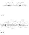
- FIG. 1Ashows, in section the initial metal core structure incorporating the invention
- FIG. 1Bshows the metal core structure after the addition of two additional functional layers on respective glass fiber layers, incorporating the invention
- FIG. 1Cshows a five-layer structure incorporating the invention
- FIG. 1Dshows the use of a solder mask coating on the structure of FIG. 1C
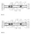
- FIG. 2illustrates a type 1 via according to the invention
- FIG. 3illustrates a type 2 via according to the invention
- FIG. 4illustrates a type 3 via according to the invention
- FIG. 5illustrates a sectional view of an overall structure incorporating the invention
- FIG. 6is a perspective view of a finished BGA IC package with a substrate incorporating the invention, mounted on a PWB which can either be of a conventional laminated board or one that incorporates the invention.
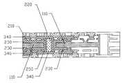
- FIG. 1Ashows the structure during the initial metal core 110 forming stage.
- FIG. 1Bshows the structure after the first two build up layers 120 are fabricated.
- FIG. 1Bshows two drilled Plated Through Holes (PTH) 220 in the structure. It can be the complete PWB structure if a 3-layer structure 210 - 110 - 210 is desired, which is simpler and less costly. Please note that the 1 ⁇ 3 oz copper foil 210 and the 5-10 oz copper core 110 are separated with insulating glass fiber prepreg layers 230 . Also the blind or laser drilled & plated via 240 is used for connecting to the core 110 as ground.
- the five-layer structure in FIG. 1Cis intended for more complex and high density applications.
- FIG. 1Cis intended for more complex and high density applications.
- FIG. 1Cshows two extra build-up layers 310 , with build-up vias 320 , and a PTH 220 .
- FIG. 1Cshows two extra build-up layers 310 , with build-up vias 320 , and a PTH 220 .
- Type 1 via 220 as illustrated in FIG. 2is for implementing the majority of the vias in the structure also shown in FIG. 1B, FIG. 1 C. It is isolated from the core and is connected to the outer layers through build-up vias 320 that are either laser drilled or controlled depth mechanically drilled.
- Type 2 viais a via that is connected with the core, which is typically used as a ground plane. It is implemented by a through hole drill 330 directly on the core 110 and followed by plating, which results in side-wall connection with the core.
- the advantage of the type 2 viais that it provides a direct thermal transfer path from the top layer 310 to the core 110 and then to the bottom layer 350 , ideal for implementing thermal vias in packaging applications.
- the only drawback with type 2 viais that the side-wall plating has interface with various layers including the core 110 and the prepreg 230 , as well as with the interface between the conductive layers 210 , 310 and the prepreg, which if not properly processed, will contain micro-cracks that allow moisture to penetrate through. The micro-cracks may result in delamination of the interface between the core 110 and the prepreg 230 .
- Type 3 viais also a via that connects to the ground plane on the core 110 , and also provides good thermal path to the core 110 . It is implemented by build-up core vias 240 and 320 through laser or controlled depth drill, also shown in FIG. 1 B and FIG. 1 C. It is good for thermal performance and does not have the reliability drawback as does the type 2 via.
- the preferred choice of the metal core 110is copper C 194 foil of 5-10 oz, or 5-15 mils thickness, as shown in FIG. 1 A.
- the liquid to plug the metal core holes 120can be PHP 900 or equivalent materials.
- the inner prepreg 230is either BT (bismaleimide triazine) or 47 N with glass fiber, of 1.5 to 3 mil thickness.
- the glass fiber ingredientallows for structural enhancement against thermal expansion coefficient mismatch between the metal core 110 and the prepreg material 230 .
- the outer prepreg 340can be either B.T. or R.C.C. (Resin-Coated-Copper) material, typically used for laser-drilled build-up.
- the thickness of the outer preg 340is also within the range of 1.5 to 3 mils.
- the copper foil 210 used in the non-core layerscan be of 1 ⁇ 3 oz thickness, though a wide thickness range is appropriate (1 ⁇ 8, ⁇ fraction (1/4 ) ⁇ , or ⁇ fraction (1/2 ) ⁇ oz) for various applications.
- Singulation lines at the border of each substrate unitcan be pre-drilled or pre-etched, during the first via drill-etch step, for easy singulation in strip or singulated delivery format.
- Liquid (PHP 900 )plug the holes 120 (as the hatched areas shown in FIG. 1 A).
- the liquid plugging 120may not be necessary, as the inner prepreg 230 will naturally flow and fill the holes during lamination. For thick cores, it is better to plug the holes first.
- 3-mil prepregs with 1 ⁇ 3 oz copper foilis used in FIG. 1 C. Note that for the reason of maintaining symmetry, one prepreg layer for each of the top and the bottom side is laminated at the same time.
- Drill holes for the through vias isolated from the coreis about 10 mils laser drill or controlled-depth mechanical drill for vias that are to be connected to the core, with the diameter in the range of 2 mils to 6 mils, as shown in FIG. 1 B.
- the liquid plugging material 120which is the prepreg that flows into the first drill hole in step 2 , isolates the plated vias 220 from the core 110 .
- Transfer inner layers 210 and 250images to form pads and trace circuitry.
- Laminate outer prepreg layers 310 and 340 with BT or R.C.C. materialIf a 3-layer only structure is desired, the outer prepreg layers 310 and 340 are not needed. With the same principle, if a 4-layer only structure is desired, then the bottom BT or R.C.C. layer is not required.
- the rest of the stepsdepend on Ni/Au plating technology and application needs. This includes imaging transfer for outer layers and Ni/Au plating 420 .
- FinishingSingulating the panel into individual units or into strips for packaging assembly.
- Singulation lines at the border of each substrate unitcan be pre-drilled or pre-etched, during the first via drill-etch step, for easy singulation in strip or singulated delivery format.
Landscapes
- Engineering & Computer Science (AREA)
- Microelectronics & Electronic Packaging (AREA)
- Manufacturing & Machinery (AREA)
- Condensed Matter Physics & Semiconductors (AREA)
- Materials Engineering (AREA)
- Physics & Mathematics (AREA)
- Chemical & Material Sciences (AREA)
- General Physics & Mathematics (AREA)
- Computer Hardware Design (AREA)
- Power Engineering (AREA)
- Production Of Multi-Layered Print Wiring Board (AREA)
- Printing Elements For Providing Electric Connections Between Printed Circuits (AREA)
- Insulated Metal Substrates For Printed Circuits (AREA)
Abstract
Description
The present application is based on provisional application Serial No. 60/128,948 filed Apr. 13, 1999 entitled METAL CORE SUBSTRATE ENABLING THERMALLY ENHANCED BALL GRID ARRAY PACKAGES.
The C2BGAs are fabricated using a complicated etching donut isolation method, resulting in copper islands on the core that are suspended by some isolation material, and then followed by surface processing and photo via steps. The incurred cost for the complex steps and the resulting complex structure is significant.
The Ball Grid Array (BGA) is an advanced array package for fine pitch, high pin count semiconductor packaging, which is used normally in a multiple-layer chip-up printed wiring board (PWB) substrate for housing the integrated circuit structure in today's IC industry. However, the heat dissipation is a major concern with the arrival of high speed CPUs such as the Pentium II & III, as well as high speed graphics, networking, DSP, and programmable logic chips. Better thermal BGA packaging solutions are required to fulfill the need of IC products in the 21 century.
The object of this invention is to provide a new and simpler PWB structure and method with comparable or better thermal performance, resulting in lower cost and better reliability. High degree of flexibility in choice of material and layer counts and layer thickness allows for a wide range of applications in packaging and high density printed circuit board or PWB. The plated copper vias also allow for better thermal performance and result in better overall thermal performance for the resulting package.
The processing steps are also ones that have proven to be practical for implementing high density interconnect for packaging applications.
The above and other objects, advantages and features of the invention will become more apparent when considered with the following description when taken in conjunction with the accompanying drawings in which like reference characters identify corresponding components or elements and wherein:
FIG. 1A shows, in section the initial metal core structure incorporating the invention,
FIG. 1B shows the metal core structure after the addition of two additional functional layers on respective glass fiber layers, incorporating the invention,
FIG. 1C shows a five-layer structure incorporating the invention,
FIG. 1D shows the use of a solder mask coating on the structure of FIG. 1C,
FIG. 2 illustrates a type1 via according to the invention,
FIG. 3 illustrates a type2 via according to the invention,
FIG. 4 illustrates a type3 via according to the invention,
FIG. 5 illustrates a sectional view of an overall structure incorporating the invention, and
FIG. 6 is a perspective view of a finished BGA IC package with a substrate incorporating the invention, mounted on a PWB which can either be of a conventional laminated board or one that incorporates the invention.
FIG. 1A shows the structure during theinitial metal core 110 forming stage. FIG. 1B shows the structure after the first two build uplayers 120 are fabricated. FIG. 1B shows two drilled Plated Through Holes (PTH)220 in the structure. It can be the complete PWB structure if a 3-layer structure210-110-210 is desired, which is simpler and less costly. Please note that the ⅓oz copper foil 210 and the 5-10oz copper core 110 are separated with insulating glassfiber prepreg layers 230. Also the blind or laser drilled & plated via240 is used for connecting to thecore 110 as ground. The five-layer structure in FIG. 1C is intended for more complex and high density applications. FIG. 1C shows two extra build-up layers 310, with build-up vias 320, and aPTH 220. In the following discussion, we will focus on the five-layer structure depicted in FIG. 1C, which includes three distinct types of vias implemented in the invention.
Type1 via220 as illustrated in FIG. 2, is for implementing the majority of the vias in the structure also shown in FIG. 1B, FIG.1C. It is isolated from the core and is connected to the outer layers through build-up vias 320 that are either laser drilled or controlled depth mechanically drilled.
Type2 via, as illustrated in FIG. 3, is a via that is connected with the core, which is typically used as a ground plane. It is implemented by athrough hole drill 330 directly on thecore 110 and followed by plating, which results in side-wall connection with the core.
The advantage of the type2 via is that it provides a direct thermal transfer path from thetop layer 310 to thecore 110 and then to thebottom layer 350, ideal for implementing thermal vias in packaging applications.
The only drawback with type2 via is that the side-wall plating has interface with various layers including thecore 110 and theprepreg 230, as well as with the interface between theconductive layers core 110 and theprepreg 230.
Type3 via, as illustrated in FIG. 4, is also a via that connects to the ground plane on thecore 110, and also provides good thermal path to thecore 110. It is implemented by build-upcore vias
The preferred choice of themetal core 110 is copper C194 foil of 5-10 oz, or 5-15 mils thickness, as shown in FIG.1A. The liquid to plug themetal core holes 120 can be PHP900 or equivalent materials.
Theinner prepreg 230 is either BT (bismaleimide triazine) or47N with glass fiber, of 1.5 to 3 mil thickness. The glass fiber ingredient allows for structural enhancement against thermal expansion coefficient mismatch between themetal core 110 and theprepreg material 230.
Theouter prepreg 340 can be either B.T. or R.C.C. (Resin-Coated-Copper) material, typically used for laser-drilled build-up. The thickness of the outer preg340 is also within the range of 1.5 to 3 mils. Thecopper foil 210 used in the non-core layers can be of ⅓ oz thickness, though a wide thickness range is appropriate (⅛, {fraction (1/4 )}, or {fraction (1/2 )} oz) for various applications.
The following describes a preferred process step sequence, though variations can be adopted by those familiar with the art of printed circuit board and HDI (high density interconnect) fabrication.
1. Starting with themetal core 110, drill or etch holes at the through-core vias sites, as shown in FIG.1B and FIG. 1C, with hole sizes around 25 mils (15 mil to 40 mils is the allowable range for BGA applications). Note that typical panel sizes are 12″×18″, or 18″×24″, or variations hereof. Black oxide processing is performed on the metal surface for better adhesion to thelaminated prepreg layer
Singulation lines at the border of each substrate unit can be pre-drilled or pre-etched, during the first via drill-etch step, for easy singulation in strip or singulated delivery format.
2. Liquid (PHP900) plug the holes120 (as the hatched areas shown in FIG.1A). In the case of athinner core 110, such as around 5 mils, the liquid plugging120 may not be necessary, as theinner prepreg 230 will naturally flow and fill the holes during lamination. For thick cores, it is better to plug the holes first.
3. Prepreg laminations230 and340.
For example, 3-mil prepregs with ⅓ oz copper foil is used in FIG.1C. Note that for the reason of maintaining symmetry, one prepreg layer for each of the top and the bottom side is laminated at the same time.
4. Drill holes for the through vias isolated from the core. The diameter of the drill is about 10 mils laser drill or controlled-depth mechanical drill for vias that are to be connected to the core, with the diameter in the range of 2 mils to 6 mils, as shown in FIG.1B. Note that theliquid plugging material 120 which is the prepreg that flows into the first drill hole in step2, isolates the plated vias220 from thecore 110.
5. Transferinner layers
6. Laminate outer prepreg layers310 and340 with BT or R.C.C. material. If a 3-layer only structure is desired, the outer prepreg layers310 and340 are not needed. With the same principle, if a 4-layer only structure is desired, then the bottom BT or R.C.C. layer is not required.
7. Form build-up viaholes 320 by Laser hole drill or controlled-depth mechanical drill.
8. Mechanical through hole drill for type2 via330 if desired.
9. Platingcopper
10. The rest of the steps depend on Ni/Au plating technology and application needs. This includes imaging transfer for outer layers and Ni/Au plating420.
11.Solder mask 410 coating, as shown in FIG. D.
12. Finishing: Singulating the panel into individual units or into strips for packaging assembly.
1. Efficient symmetric layer and via structures for high thermal conductance.
2. Achieving same or better thermal performance comparing to prior art, with mature processing technology and proven materials.
3. Requires only incremental cost increase for offering better performance than Plastic Ball Grid Array (PBGA).
1. New copper-core based structure for chip-up high thermal performance package using 3-layer (core+1-top+1-bottom), 4-layer (core+2-top+1-bottom), and 5-layer (core+2-top+2-bottom). Moreover, 5 or more layers can be built easily. The 3-and 5-layer options are symmetric, with better warpage prevention.
2. The use of drilling/etching, optional liquid-filled, laminating, drilling, and plating process steps for forming the through core via holes.
3. The combination of laser blind vias build-up on top of the metal core structure, enabling additional build-up layers for high density applications.
4. Efficient thermal vias by plating build-up and connecting to the core from both the top and bottom sides.
5. Singulation lines at the border of each substrate unit can be pre-drilled or pre-etched, during the first via drill-etch step, for easy singulation in strip or singulated delivery format.
6. Applications: a) Metal core based substrates for thermally enhanced fine-pitch BGAS, and b) Metal core based high density boards such as for high thermal output SDRAM DIMM modules.
While the invention has been described in relation to preferred embodiments of the invention, it will be appreciated that other embodiments, adaptations and modifications of the invention will be apparent to those skilled in the art.
Claims (11)
1. A method of making a thermally enhanced printed circuit wiring board substrate for ball grid integrated circuit packages comprising the steps of:
a) providing an initial thin conductive metal core having oppositely facing surfaces,
b) forming one or more holes in said metal core at each of a plurality of through-core via sites,
c) laminating a thin rigidifying non-conductive dielectric sheet to each said oppositely facing surfaces, respectively,
d) forming at least one via to said metal core in one of said dielectric sheets,
e) applying at least one thin conductive layer on a surface of one of said thin rigidifying non-conductive sheets and making at least one electrical connection to said initial thin conductive metal core at said at least one via to said metal core.
2. The method defined inclaim 1 further including a step of making one or more of Type1 vias at said one or more through-core via sites.
3. The method defined inclaim 1 further including a step of forming one or more Type2 vias at said one or more through-core via sites.
4. The method defined inclaim 1 further including a step of forming one or more Type3 vias at one or more said metal core vias.
5. The method defined inclaim 2 further including a step of forming one or more Type2 or Type3 vias at said one or more through-core via sites.
6. The method defined inclaim 4 wherein said Type3 via of is isolated from said core and connected to the thin conductive layer.
7. The method defined inclaim 3 wherein said Type2 vias are made by through-hole plating directly to said core and followed by plating resulting in sidewall connection with the core.
8. The method defined inclaim 1 wherein said plurality of through-core via sites are drilled, plated through-holes (PTH).
9. The method defined inclaim 1 wherein said through-core vias are made by printing build-up and connection to the core in the opposite facing surfaces.
10. A method of making a thermally enhanced printed circuit wiring board substrate for ball grid integrated circuit packages comprising the steps of:
a) providing an initial thin conductive metal core having oppositely facing surfaces,
b) forming one or more holes in said metal core at each of a plurality of through-core via sites,
c) laminating a thin rigidifying non-conductive dielectric sheet to each said oppositely facing surfaces, respectively, so that at least one exposed surface of the non-conductive dielectric sheet facing outwardly, respectively,
d) applying at least one thin conductive layer on said at least one exposed surface of non-conductive dielectric sheet, and
e) forming a conductive connection between said thin conductive layer on said surface through one of said through-core via sites.
11. The method defined inclaim 10 further including forming at least one via to said metal core in at least one of said dielectric sheets, and
making at least one electric connection to said initial thin conductive metal core at said at least one via to said metal core.
Priority Applications (7)
| Application Number | Priority Date | Filing Date | Title |
|---|---|---|---|
| US09/544,263US6711812B1 (en) | 1999-04-13 | 2000-04-06 | Method of making metal core substrate printed circuit wiring board enabling thermally enhanced ball grid array (BGA) packages |
| TW089106768ATW463537B (en) | 1999-04-13 | 2000-04-12 | Metal core substrate printed wiring board enabling thermally enhanced ball grid array (BGA) packages and method |
| JP2000611313AJP2002541680A (en) | 1999-04-13 | 2000-04-13 | Printed wiring board with metal core substrate for heat strengthening of ball grid array package and method of manufacturing the same |
| CNB008061432ACN1157773C (en) | 1999-04-13 | 2000-04-13 | Metal core substrate printed wiring board for thermally enhanced ball grid array package and method |
| PCT/IB2000/000611WO2000062337A1 (en) | 1999-04-13 | 2000-04-13 | Metal core substrate printed wiring board enabling thermally enhanced ball grid array (bga) packages and method |
| AU41395/00AAU4139500A (en) | 1999-04-13 | 2000-04-13 | Metal core substrate printed wiring board enabling thermally enhanced ball grid array (bga) packages and method |
| US10/784,813US20040163248A1 (en) | 1999-04-13 | 2004-02-24 | Metal core substrate printed wiring board enabling thermally enhanced ball grid array ( BGA) packages and method |
Applications Claiming Priority (2)
| Application Number | Priority Date | Filing Date | Title |
|---|---|---|---|
| US12894899P | 1999-04-13 | 1999-04-13 | |
| US09/544,263US6711812B1 (en) | 1999-04-13 | 2000-04-06 | Method of making metal core substrate printed circuit wiring board enabling thermally enhanced ball grid array (BGA) packages |
Related Child Applications (1)
| Application Number | Title | Priority Date | Filing Date |
|---|---|---|---|
| US10/784,813DivisionUS20040163248A1 (en) | 1999-04-13 | 2004-02-24 | Metal core substrate printed wiring board enabling thermally enhanced ball grid array ( BGA) packages and method |
Publications (1)
| Publication Number | Publication Date |
|---|---|
| US6711812B1true US6711812B1 (en) | 2004-03-30 |
Family
ID=26827102
Family Applications (2)
| Application Number | Title | Priority Date | Filing Date |
|---|---|---|---|
| US09/544,263Expired - Fee RelatedUS6711812B1 (en) | 1999-04-13 | 2000-04-06 | Method of making metal core substrate printed circuit wiring board enabling thermally enhanced ball grid array (BGA) packages |
| US10/784,813AbandonedUS20040163248A1 (en) | 1999-04-13 | 2004-02-24 | Metal core substrate printed wiring board enabling thermally enhanced ball grid array ( BGA) packages and method |
Family Applications After (1)
| Application Number | Title | Priority Date | Filing Date |
|---|---|---|---|
| US10/784,813AbandonedUS20040163248A1 (en) | 1999-04-13 | 2004-02-24 | Metal core substrate printed wiring board enabling thermally enhanced ball grid array ( BGA) packages and method |
Country Status (6)
| Country | Link |
|---|---|
| US (2) | US6711812B1 (en) |
| JP (1) | JP2002541680A (en) |
| CN (1) | CN1157773C (en) |
| AU (1) | AU4139500A (en) |
| TW (1) | TW463537B (en) |
| WO (1) | WO2000062337A1 (en) |
Cited By (20)
| Publication number | Priority date | Publication date | Assignee | Title |
|---|---|---|---|---|
| US20040012097A1 (en)* | 2002-07-17 | 2004-01-22 | Chien-Wei Chang | Structure and method for fine pitch flip chip substrate |
| US20050003575A1 (en)* | 2003-07-05 | 2005-01-06 | Tan Yong Kian | Apparatus, systems and methods relating to the reconstruction of semiconductor wafers for wafer-level processing and reconstructed semiconductor wafers |
| US20050150683A1 (en)* | 2004-01-12 | 2005-07-14 | Farnworth Warren M. | Methods of fabricating substrates and substrate precursor structures resulting therefrom |
| US20050178657A1 (en)* | 2003-10-09 | 2005-08-18 | Kirby Kyle K. | Systems and methods of plating via interconnects |
| US20060137907A1 (en)* | 2004-12-29 | 2006-06-29 | Hewlett-Packard Development Company, L.P. | Component for impedance matching |
| FR2885480A1 (en)* | 2005-05-04 | 2006-11-10 | Bree Beauce Realisations Et Et | DOUBLE-SIDED PRINTED CIRCUIT WITH THERMAL DISSIPATION |
| US20070166991A1 (en)* | 2003-09-23 | 2007-07-19 | Nishant Sinha | Methods for forming conductive vias in semiconductor device components |
| US20070261234A1 (en)* | 2006-05-10 | 2007-11-15 | Samsung Electro-Mechanics Co., Ltd. | Method of manufacturing build-up printed circuit board |
| US20070291457A1 (en)* | 2006-06-16 | 2007-12-20 | Huili Fu | IC packages with internal heat dissipation structures |
| US20080011507A1 (en)* | 2006-07-14 | 2008-01-17 | Vasoya Kalu K | Build-up printed wiring board substrate having a core layer that is part of a circuit |
| US20090103274A1 (en)* | 2005-06-24 | 2009-04-23 | Nxp B.V. | Warpage preventing substrates and method of making same |
| US20140124944A1 (en)* | 2012-11-05 | 2014-05-08 | Nvidia Corporation | Substrate build up layer to achieve both finer design rule and better package coplanarity |
| US8848313B1 (en)* | 2006-01-13 | 2014-09-30 | Marvell International Ltd. | Thermal solution for drive systems such as hard disk drives and digital versatile discs |
| USRE45637E1 (en) | 2005-08-29 | 2015-07-28 | Stablcor Technology, Inc. | Processes for manufacturing printed wiring boards |
| US9332632B2 (en) | 2014-08-20 | 2016-05-03 | Stablcor Technology, Inc. | Graphene-based thermal management cores and systems and methods for constructing printed wiring boards |
| US20160286660A1 (en)* | 2015-03-25 | 2016-09-29 | International Business Machines Corporation | Glass interposer with thermal vias |
| US9554462B2 (en)* | 2014-03-07 | 2017-01-24 | Ibiden Co., Ltd. | Printed wiring board |
| US9781611B2 (en) | 2008-03-28 | 2017-10-03 | Marvell World Trade Ltd. | Boosted, dedicated reference signal |
| US9788436B2 (en) | 2013-04-17 | 2017-10-10 | The United State Of America As Represented By The Secretary Of The Army | Method of making a non-planar circuit board with embedded electronic components on a mandrel |
| US10790426B2 (en)* | 2016-04-01 | 2020-09-29 | Nichia Corporation | Method of manufacturing light emitting element mounting base member, method of manufacturing light emitting device using the light emitting element mounting base member, light emitting element mounting base member, and light emitting device using the light emitting element mounting base member |
Families Citing this family (5)
| Publication number | Priority date | Publication date | Assignee | Title |
|---|---|---|---|---|
| JP4339739B2 (en) | 2004-04-26 | 2009-10-07 | 太陽誘電株式会社 | Multi-layer board with built-in components |
| US7602062B1 (en)* | 2005-08-10 | 2009-10-13 | Altera Corporation | Package substrate with dual material build-up layers |
| US20090141456A1 (en)* | 2007-11-30 | 2009-06-04 | Itt Manufacturing Enterprises, Inc. | Multilayer, thermally-stabilized substrate structures |
| JP5874309B2 (en)* | 2011-10-21 | 2016-03-02 | 富士通株式会社 | Wiring board and manufacturing method thereof |
| TWI582925B (en)* | 2015-02-04 | 2017-05-11 | 智威科技股份有限公司 | Semiconductor package structure and manufacturing method thereof |
Citations (25)
| Publication number | Priority date | Publication date | Assignee | Title |
|---|---|---|---|---|
| US3401126A (en) | 1965-06-18 | 1968-09-10 | Ibm | Method of rendering noble metal conductive composition non-wettable by solder |
| US3429040A (en) | 1965-06-18 | 1969-02-25 | Ibm | Method of joining a component to a substrate |
| US3436818A (en) | 1965-12-13 | 1969-04-08 | Ibm | Method of fabricating a bonded joint |
| US3564522A (en) | 1966-12-16 | 1971-02-16 | Data Disc Inc | Transducer with thin film coil and semiconductor switching |
| US3949125A (en) | 1965-05-14 | 1976-04-06 | Roberts Arthur H | Molded solid plastics articles and a method for their manufacture |
| US4229248A (en) | 1979-04-06 | 1980-10-21 | Intel Magnetics, Inc. | Process for forming bonding pads on magnetic bubble devices |
| US4462534A (en) | 1981-12-29 | 1984-07-31 | International Business Machines Corporation | Method of bonding connecting pins to the eyelets of conductors formed on a ceramic substrate |
| US4504283A (en) | 1982-07-22 | 1985-03-12 | Superior Finishers, Incorporated | Cushioned abrasive articles, and method of manufacture |
| US4546541A (en) | 1983-10-14 | 1985-10-15 | Applied Magnetics Corporation | Method of attaching electrical conductors to thin film magnetic transducer |
| US4579806A (en) | 1983-09-02 | 1986-04-01 | Basf Aktiengesellschaft | Positive-working photosensitive recording materials |
| US4761699A (en) | 1986-10-28 | 1988-08-02 | International Business Machines Corporation | Slider-suspension assembly and method for attaching a slider to a suspension in a data recording disk file |
| US4818728A (en) | 1986-12-03 | 1989-04-04 | Sharp Kabushiki Kaisha | Method of making a hybrid semiconductor device |
| US4825284A (en) | 1985-12-11 | 1989-04-25 | Hitachi, Ltd. | Semiconductor resin package structure |
| US4864471A (en) | 1985-09-30 | 1989-09-05 | Siemens Aktiengesellschaft | Component for surface mounting and method for fastening a component for surface mounting |
| US4996623A (en) | 1989-08-07 | 1991-02-26 | International Business Machines Corporation | Laminated suspension for a negative pressure slider in a data recording disk file |
| US4999699A (en) | 1990-03-14 | 1991-03-12 | International Business Machines Corporation | Solder interconnection structure and process for making |
| US5121190A (en) | 1990-03-14 | 1992-06-09 | International Business Machines Corp. | Solder interconnection structure on organic substrates |
| US5128746A (en) | 1990-09-27 | 1992-07-07 | Motorola, Inc. | Adhesive and encapsulant material with fluxing properties |
| US5334857A (en) | 1992-04-06 | 1994-08-02 | Motorola, Inc. | Semiconductor device with test-only contacts and method for making the same |
| US5378859A (en) | 1992-03-02 | 1995-01-03 | Casio Computer Co., Ltd. | Film wiring board |
| US5541446A (en) | 1994-08-29 | 1996-07-30 | Analog Devices, Inc. | Integrated circuit package with improved heat dissipation |
| US5574629A (en) | 1989-06-09 | 1996-11-12 | Sullivan; Kenneth W. | Solderless printed wiring devices |
| US5796159A (en) | 1995-11-30 | 1998-08-18 | Analog Devices, Inc. | Thermally efficient integrated circuit package |
| US5844308A (en) | 1997-08-20 | 1998-12-01 | Cts Corporation | Integrated circuit anti-bridging leads design |
| US6083340A (en)* | 1997-02-28 | 2000-07-04 | Hokuriku Electric Industry Co., Ltd. | Process for manufacturing a multi-layer circuit board |
Family Cites Families (12)
| Publication number | Priority date | Publication date | Assignee | Title |
|---|---|---|---|---|
| US4817280A (en)* | 1985-06-10 | 1989-04-04 | O. Key Printed Wiring Co., Ltd. | Method of manufacturing printed circuit boards |
| US5247246A (en)* | 1987-04-17 | 1993-09-21 | Everett Charles Technologies, Inc. | Testing of integrated circuit devices on loaded printed circuit boards |
| US5861076A (en)* | 1991-07-19 | 1999-01-19 | Park Electrochemical Corporation | Method for making multi-layer circuit boards |
| JPH05183275A (en)* | 1991-12-27 | 1993-07-23 | Yokohama Rubber Co Ltd:The | Manufacture of metal core multilayer printed wiring board |
| US5282312A (en)* | 1991-12-31 | 1994-02-01 | Tessera, Inc. | Multi-layer circuit construction methods with customization features |
| US5306670A (en)* | 1993-02-09 | 1994-04-26 | Texas Instruments Incorporated | Multi-chip integrated circuit module and method for fabrication thereof |
| JP3513983B2 (en)* | 1994-07-25 | 2004-03-31 | 凸版印刷株式会社 | Manufacturing method of chip carrier |
| US5509200A (en)* | 1994-11-21 | 1996-04-23 | International Business Machines Corporation | Method of making laminar stackable circuit board structure |
| US6204453B1 (en)* | 1998-12-02 | 2001-03-20 | International Business Machines Corporation | Two signal one power plane circuit board |
| US5847327A (en)* | 1996-11-08 | 1998-12-08 | W.L. Gore & Associates, Inc. | Dimensionally stable core for use in high density chip packages |
| US6639155B1 (en)* | 1997-06-11 | 2003-10-28 | International Business Machines Corporation | High performance packaging platform and method of making same |
| JP3834426B2 (en)* | 1997-09-02 | 2006-10-18 | 沖電気工業株式会社 | Semiconductor device |
- 2000
- 2000-04-06USUS09/544,263patent/US6711812B1/ennot_activeExpired - Fee Related
- 2000-04-12TWTW089106768Apatent/TW463537B/enactive
- 2000-04-13JPJP2000611313Apatent/JP2002541680A/enactivePending
- 2000-04-13AUAU41395/00Apatent/AU4139500A/ennot_activeAbandoned
- 2000-04-13CNCNB008061432Apatent/CN1157773C/ennot_activeExpired - Fee Related
- 2000-04-13WOPCT/IB2000/000611patent/WO2000062337A1/enactiveApplication Filing
- 2004
- 2004-02-24USUS10/784,813patent/US20040163248A1/ennot_activeAbandoned
Patent Citations (25)
| Publication number | Priority date | Publication date | Assignee | Title |
|---|---|---|---|---|
| US3949125A (en) | 1965-05-14 | 1976-04-06 | Roberts Arthur H | Molded solid plastics articles and a method for their manufacture |
| US3401126A (en) | 1965-06-18 | 1968-09-10 | Ibm | Method of rendering noble metal conductive composition non-wettable by solder |
| US3429040A (en) | 1965-06-18 | 1969-02-25 | Ibm | Method of joining a component to a substrate |
| US3436818A (en) | 1965-12-13 | 1969-04-08 | Ibm | Method of fabricating a bonded joint |
| US3564522A (en) | 1966-12-16 | 1971-02-16 | Data Disc Inc | Transducer with thin film coil and semiconductor switching |
| US4229248A (en) | 1979-04-06 | 1980-10-21 | Intel Magnetics, Inc. | Process for forming bonding pads on magnetic bubble devices |
| US4462534A (en) | 1981-12-29 | 1984-07-31 | International Business Machines Corporation | Method of bonding connecting pins to the eyelets of conductors formed on a ceramic substrate |
| US4504283A (en) | 1982-07-22 | 1985-03-12 | Superior Finishers, Incorporated | Cushioned abrasive articles, and method of manufacture |
| US4579806A (en) | 1983-09-02 | 1986-04-01 | Basf Aktiengesellschaft | Positive-working photosensitive recording materials |
| US4546541A (en) | 1983-10-14 | 1985-10-15 | Applied Magnetics Corporation | Method of attaching electrical conductors to thin film magnetic transducer |
| US4864471A (en) | 1985-09-30 | 1989-09-05 | Siemens Aktiengesellschaft | Component for surface mounting and method for fastening a component for surface mounting |
| US4825284A (en) | 1985-12-11 | 1989-04-25 | Hitachi, Ltd. | Semiconductor resin package structure |
| US4761699A (en) | 1986-10-28 | 1988-08-02 | International Business Machines Corporation | Slider-suspension assembly and method for attaching a slider to a suspension in a data recording disk file |
| US4818728A (en) | 1986-12-03 | 1989-04-04 | Sharp Kabushiki Kaisha | Method of making a hybrid semiconductor device |
| US5574629A (en) | 1989-06-09 | 1996-11-12 | Sullivan; Kenneth W. | Solderless printed wiring devices |
| US4996623A (en) | 1989-08-07 | 1991-02-26 | International Business Machines Corporation | Laminated suspension for a negative pressure slider in a data recording disk file |
| US4999699A (en) | 1990-03-14 | 1991-03-12 | International Business Machines Corporation | Solder interconnection structure and process for making |
| US5121190A (en) | 1990-03-14 | 1992-06-09 | International Business Machines Corp. | Solder interconnection structure on organic substrates |
| US5128746A (en) | 1990-09-27 | 1992-07-07 | Motorola, Inc. | Adhesive and encapsulant material with fluxing properties |
| US5378859A (en) | 1992-03-02 | 1995-01-03 | Casio Computer Co., Ltd. | Film wiring board |
| US5334857A (en) | 1992-04-06 | 1994-08-02 | Motorola, Inc. | Semiconductor device with test-only contacts and method for making the same |
| US5541446A (en) | 1994-08-29 | 1996-07-30 | Analog Devices, Inc. | Integrated circuit package with improved heat dissipation |
| US5796159A (en) | 1995-11-30 | 1998-08-18 | Analog Devices, Inc. | Thermally efficient integrated circuit package |
| US6083340A (en)* | 1997-02-28 | 2000-07-04 | Hokuriku Electric Industry Co., Ltd. | Process for manufacturing a multi-layer circuit board |
| US5844308A (en) | 1997-08-20 | 1998-12-01 | Cts Corporation | Integrated circuit anti-bridging leads design |
Cited By (47)
| Publication number | Priority date | Publication date | Assignee | Title |
|---|---|---|---|---|
| US20050032273A1 (en)* | 2002-07-17 | 2005-02-10 | Chien-Wei Chang | Structure and method for fine pitch flip chip substrate |
| US20040012097A1 (en)* | 2002-07-17 | 2004-01-22 | Chien-Wei Chang | Structure and method for fine pitch flip chip substrate |
| US6969674B2 (en)* | 2002-07-17 | 2005-11-29 | Kinsus Interconnect Technology | Structure and method for fine pitch flip chip substrate |
| US20050263517A1 (en)* | 2003-07-05 | 2005-12-01 | Tan Yong K | Apparatus relating to the reconstruction of semiconductor wafers for wafer-level processing |
| US20050003575A1 (en)* | 2003-07-05 | 2005-01-06 | Tan Yong Kian | Apparatus, systems and methods relating to the reconstruction of semiconductor wafers for wafer-level processing and reconstructed semiconductor wafers |
| US7573006B2 (en) | 2003-07-05 | 2009-08-11 | Micron Technology, Inc. | Apparatus relating to the reconstruction of semiconductor wafers for wafer-level processing |
| US9287207B2 (en) | 2003-09-23 | 2016-03-15 | Micron Technology, Inc. | Methods for forming conductive vias in semiconductor device components |
| US8148263B2 (en) | 2003-09-23 | 2012-04-03 | Micron Technology, Inc. | Methods for forming conductive vias in semiconductor device components |
| US7666788B2 (en) | 2003-09-23 | 2010-02-23 | Micron Technology, Inc. | Methods for forming conductive vias in semiconductor device components |
| US20070166991A1 (en)* | 2003-09-23 | 2007-07-19 | Nishant Sinha | Methods for forming conductive vias in semiconductor device components |
| US7608904B2 (en) | 2003-09-23 | 2009-10-27 | Micron Technology, Inc. | Semiconductor device components with conductive vias and systems including the components |
| US20070170595A1 (en)* | 2003-09-23 | 2007-07-26 | Nishant Sinha | Semiconductor device components with conductive vias and systems including the components |
| US20060180940A1 (en)* | 2003-10-09 | 2006-08-17 | Kirby Kyle K | Semiconductor devices and in-process semiconductor devices having conductor filled vias |
| US7701039B2 (en) | 2003-10-09 | 2010-04-20 | Micron Technology, Inc. | Semiconductor devices and in-process semiconductor devices having conductor filled vias |
| US20050178657A1 (en)* | 2003-10-09 | 2005-08-18 | Kirby Kyle K. | Systems and methods of plating via interconnects |
| US7594322B2 (en) | 2004-01-12 | 2009-09-29 | Micron Technology, Inc. | Methods of fabricating substrates including at least one conductive via |
| US7603772B2 (en) | 2004-01-12 | 2009-10-20 | Micron Technology, Inc. | Methods of fabricating substrates including one or more conductive vias |
| US20050150683A1 (en)* | 2004-01-12 | 2005-07-14 | Farnworth Warren M. | Methods of fabricating substrates and substrate precursor structures resulting therefrom |
| US20080060193A1 (en)* | 2004-01-12 | 2008-03-13 | Micron Technology, Inc. | Methods of fabricating substrates including at least one conductive via |
| US7316063B2 (en) | 2004-01-12 | 2008-01-08 | Micron Technology, Inc. | Methods of fabricating substrates including at least one conductive via |
| US20060254808A1 (en)* | 2004-01-12 | 2006-11-16 | Farnworth Warren M | Substrate precursor structures |
| US20070169343A1 (en)* | 2004-01-12 | 2007-07-26 | Farnworth Warren M | Methods of fabricating substrates including one or more conductive vias |
| US20060137907A1 (en)* | 2004-12-29 | 2006-06-29 | Hewlett-Packard Development Company, L.P. | Component for impedance matching |
| US7652896B2 (en)* | 2004-12-29 | 2010-01-26 | Hewlett-Packard Development Company, L.P. | Component for impedance matching |
| FR2885480A1 (en)* | 2005-05-04 | 2006-11-10 | Bree Beauce Realisations Et Et | DOUBLE-SIDED PRINTED CIRCUIT WITH THERMAL DISSIPATION |
| EP1720391A3 (en)* | 2005-05-04 | 2008-04-23 | BREE (Beauce Réalisations et Études Électroniques) | Double-sided printed circuit board with thermal dissipation |
| US8383954B2 (en)* | 2005-06-24 | 2013-02-26 | Taiwan Semiconductor Manufacturing Company, Ltd. | Warpage preventing substrates |
| US20090103274A1 (en)* | 2005-06-24 | 2009-04-23 | Nxp B.V. | Warpage preventing substrates and method of making same |
| USRE45637E1 (en) | 2005-08-29 | 2015-07-28 | Stablcor Technology, Inc. | Processes for manufacturing printed wiring boards |
| US8848313B1 (en)* | 2006-01-13 | 2014-09-30 | Marvell International Ltd. | Thermal solution for drive systems such as hard disk drives and digital versatile discs |
| US7707716B2 (en)* | 2006-05-10 | 2010-05-04 | Samsung Electro-Mechanics Co., Ltd. | Method of manufacturing build-up printed circuit board |
| US20070261234A1 (en)* | 2006-05-10 | 2007-11-15 | Samsung Electro-Mechanics Co., Ltd. | Method of manufacturing build-up printed circuit board |
| US8031484B2 (en) | 2006-06-16 | 2011-10-04 | Hong Kong Applied Science And Technology Research Institute Co., Ltd. | IC packages with internal heat dissipation structures |
| US20070291457A1 (en)* | 2006-06-16 | 2007-12-20 | Huili Fu | IC packages with internal heat dissipation structures |
| US9408314B2 (en) | 2006-07-14 | 2016-08-02 | Stablcor Technology Inc. | Build-up printed wiring board substrate having a core layer that is part of a circuit |
| US8203080B2 (en)* | 2006-07-14 | 2012-06-19 | Stablcor Technology, Inc. | Build-up printed wiring board substrate having a core layer that is part of a circuit |
| US20080011507A1 (en)* | 2006-07-14 | 2008-01-17 | Vasoya Kalu K | Build-up printed wiring board substrate having a core layer that is part of a circuit |
| US9781611B2 (en) | 2008-03-28 | 2017-10-03 | Marvell World Trade Ltd. | Boosted, dedicated reference signal |
| US9368439B2 (en)* | 2012-11-05 | 2016-06-14 | Nvidia Corporation | Substrate build up layer to achieve both finer design rule and better package coplanarity |
| US20140124944A1 (en)* | 2012-11-05 | 2014-05-08 | Nvidia Corporation | Substrate build up layer to achieve both finer design rule and better package coplanarity |
| US9788436B2 (en) | 2013-04-17 | 2017-10-10 | The United State Of America As Represented By The Secretary Of The Army | Method of making a non-planar circuit board with embedded electronic components on a mandrel |
| US9554462B2 (en)* | 2014-03-07 | 2017-01-24 | Ibiden Co., Ltd. | Printed wiring board |
| US9332632B2 (en) | 2014-08-20 | 2016-05-03 | Stablcor Technology, Inc. | Graphene-based thermal management cores and systems and methods for constructing printed wiring boards |
| US20160286660A1 (en)* | 2015-03-25 | 2016-09-29 | International Business Machines Corporation | Glass interposer with thermal vias |
| US9585257B2 (en)* | 2015-03-25 | 2017-02-28 | Globalfoundries Inc. | Method of forming a glass interposer with thermal vias |
| US10790426B2 (en)* | 2016-04-01 | 2020-09-29 | Nichia Corporation | Method of manufacturing light emitting element mounting base member, method of manufacturing light emitting device using the light emitting element mounting base member, light emitting element mounting base member, and light emitting device using the light emitting element mounting base member |
| US11257999B2 (en) | 2016-04-01 | 2022-02-22 | Nichia Corporation | Light emitting element mounting base member, and light emitting device using the light emitting element mounting base member |
Also Published As
| Publication number | Publication date |
|---|---|
| JP2002541680A (en) | 2002-12-03 |
| TW463537B (en) | 2001-11-11 |
| US20040163248A1 (en) | 2004-08-26 |
| CN1157773C (en) | 2004-07-14 |
| AU4139500A (en) | 2000-11-14 |
| WO2000062337A1 (en) | 2000-10-19 |
| CN1346513A (en) | 2002-04-24 |
Similar Documents
| Publication | Publication Date | Title |
|---|---|---|
| US6711812B1 (en) | Method of making metal core substrate printed circuit wiring board enabling thermally enhanced ball grid array (BGA) packages | |
| US6192581B1 (en) | Method of making printed circuit board | |
| US6930257B1 (en) | Integrated circuit substrate having laminated laser-embedded circuit layers | |
| KR101044127B1 (en) | Radiator plate and manufacturing method thereof | |
| US9775237B2 (en) | Wiring substrate and method for manufacturing the same | |
| US10098243B2 (en) | Printed wiring board and semiconductor package | |
| JPH11233678A (en) | Manufacture of ic package | |
| JP2007096262A (en) | Wiring board and ceramic chip for embedding | |
| KR100298897B1 (en) | Method for manufacturing pcb | |
| US20100108371A1 (en) | Wiring board with built-in electronic component and method for manufacturing the same | |
| JP3577421B2 (en) | Package for semiconductor device | |
| JP4497548B2 (en) | Wiring board | |
| KR100653249B1 (en) | Metal core, package substrate and manufacturing method thereof | |
| KR101167429B1 (en) | Method for manufacturing the semiconductor package | |
| US6582616B2 (en) | Method for preparing ball grid array board | |
| US6207354B1 (en) | Method of making an organic chip carrier package | |
| US8826531B1 (en) | Method for making an integrated circuit substrate having laminated laser-embedded circuit layers | |
| EP0574207A2 (en) | Multilayer printed circuit board and method for manufacturing the same | |
| KR100803960B1 (en) | Package-on Package Substrate and Manufacturing Method Thereof | |
| KR100917028B1 (en) | Metal substrate using anodizing and manufacturing method thereof | |
| JP2003229662A (en) | Method of manufacturing wiring board | |
| JP2001015912A (en) | Multilayered printed wiring board and production thereof | |
| JP2002223071A (en) | Build-up core board, build-up wiring board and method for manufacturing the same | |
| JP3877358B2 (en) | Multi-layer printed wiring board for IC mounting | |
| US20240194578A1 (en) | Embedded device package substrate and manufacturing method therefor |
Legal Events
| Date | Code | Title | Description |
|---|---|---|---|
| AS | Assignment | Owner name:UNICAP ELECTRONICS INDUSTRIAL CORPORATION, TAIWAN Free format text:ASSIGNMENT OF ASSIGNORS INTEREST;ASSIGNORS:WU, PAUL;CHEN, RAY;REEL/FRAME:011357/0040;SIGNING DATES FROM 20001006 TO 20001026 | |
| REMI | Maintenance fee reminder mailed | ||
| LAPS | Lapse for failure to pay maintenance fees | ||
| STCH | Information on status: patent discontinuation | Free format text:PATENT EXPIRED DUE TO NONPAYMENT OF MAINTENANCE FEES UNDER 37 CFR 1.362 | |
| FP | Lapsed due to failure to pay maintenance fee | Effective date:20080330 |