US6709958B2 - Integrated circuit device and fabrication using metal-doped chalcogenide materials - Google Patents
Integrated circuit device and fabrication using metal-doped chalcogenide materialsDownload PDFInfo
- Publication number
- US6709958B2 US6709958B2US09/943,426US94342601AUS6709958B2US 6709958 B2US6709958 B2US 6709958B2US 94342601 AUS94342601 AUS 94342601AUS 6709958 B2US6709958 B2US 6709958B2
- Authority
- US
- United States
- Prior art keywords
- plasma
- layer
- component
- chalcogenide
- neon
- Prior art date
- Legal status (The legal status is an assumption and is not a legal conclusion. Google has not performed a legal analysis and makes no representation as to the accuracy of the status listed.)
- Expired - Lifetime
Links
- 150000004770chalcogenidesChemical class0.000titleclaimsabstractdescription151
- 239000000463materialSubstances0.000titleclaimsdescription51
- 238000004519manufacturing processMethods0.000titledescription7
- 238000000034methodMethods0.000claimsabstractdescription83
- 229910052751metalInorganic materials0.000claimsabstractdescription70
- 239000002184metalSubstances0.000claimsabstractdescription70
- 229910052754neonInorganic materials0.000claimsabstractdescription37
- GKAOGPIIYCISHV-UHFFFAOYSA-Nneon atomChemical compound[Ne]GKAOGPIIYCISHV-UHFFFAOYSA-N0.000claimsabstractdescription37
- 238000001228spectrumMethods0.000claimsabstractdescription25
- 238000009792diffusion processMethods0.000claimsabstractdescription24
- 229910052756noble gasInorganic materials0.000claimsabstractdescription18
- 239000001307heliumSubstances0.000claimsabstractdescription15
- 229910052734heliumInorganic materials0.000claimsabstractdescription15
- SWQJXJOGLNCZEY-UHFFFAOYSA-Nhelium atomChemical compound[He]SWQJXJOGLNCZEY-UHFFFAOYSA-N0.000claimsabstractdescription15
- 238000011065in-situ storageMethods0.000claimsabstractdescription8
- 239000007789gasSubstances0.000claimsdescription65
- 238000004544sputter depositionMethods0.000claimsdescription35
- XKRFYHLGVUSROY-UHFFFAOYSA-NArgonChemical compound[Ar]XKRFYHLGVUSROY-UHFFFAOYSA-N0.000claimsdescription30
- 239000000203mixtureSubstances0.000claimsdescription21
- BQCADISMDOOEFD-UHFFFAOYSA-NSilverChemical compound[Ag]BQCADISMDOOEFD-UHFFFAOYSA-N0.000claimsdescription18
- 229910052709silverInorganic materials0.000claimsdescription18
- 239000004332silverSubstances0.000claimsdescription18
- 229910052786argonInorganic materials0.000claimsdescription15
- 238000000151depositionMethods0.000claimsdescription15
- QIHHYQWNYKOHEV-UHFFFAOYSA-N4-tert-butyl-3-nitrobenzoic acidChemical compoundCC(C)(C)C1=CC=C(C(O)=O)C=C1[N+]([O-])=OQIHHYQWNYKOHEV-UHFFFAOYSA-N0.000claimsdescription11
- 239000011669seleniumSubstances0.000claimsdescription8
- IJGRMHOSHXDMSA-UHFFFAOYSA-NAtomic nitrogenChemical compoundN#NIJGRMHOSHXDMSA-UHFFFAOYSA-N0.000claimsdescription7
- BUGBHKTXTAQXES-UHFFFAOYSA-NSeleniumChemical compound[Se]BUGBHKTXTAQXES-UHFFFAOYSA-N0.000claimsdescription6
- 239000010949copperSubstances0.000claimsdescription6
- 239000010931goldSubstances0.000claimsdescription6
- 229910052711seleniumInorganic materials0.000claimsdescription6
- 229910052714telluriumInorganic materials0.000claimsdescription6
- PORWMNRCUJJQNO-UHFFFAOYSA-Ntellurium atomChemical compound[Te]PORWMNRCUJJQNO-UHFFFAOYSA-N0.000claimsdescription6
- OKTJSMMVPCPJKN-UHFFFAOYSA-NCarbonChemical compound[C]OKTJSMMVPCPJKN-UHFFFAOYSA-N0.000claimsdescription5
- RYGMFSIKBFXOCR-UHFFFAOYSA-NCopperChemical compound[Cu]RYGMFSIKBFXOCR-UHFFFAOYSA-N0.000claimsdescription5
- 229910052782aluminiumInorganic materials0.000claimsdescription5
- XAGFODPZIPBFFR-UHFFFAOYSA-NaluminiumChemical compound[Al]XAGFODPZIPBFFR-UHFFFAOYSA-N0.000claimsdescription5
- 229910052787antimonyInorganic materials0.000claimsdescription5
- WATWJIUSRGPENY-UHFFFAOYSA-Nantimony atomChemical compound[Sb]WATWJIUSRGPENY-UHFFFAOYSA-N0.000claimsdescription5
- 229910052799carbonInorganic materials0.000claimsdescription5
- 229910052802copperInorganic materials0.000claimsdescription5
- 229910052732germaniumInorganic materials0.000claimsdescription5
- GNPVGFCGXDBREM-UHFFFAOYSA-Ngermanium atomChemical compound[Ge]GNPVGFCGXDBREM-UHFFFAOYSA-N0.000claimsdescription5
- PCHJSUWPFVWCPO-UHFFFAOYSA-NgoldChemical compound[Au]PCHJSUWPFVWCPO-UHFFFAOYSA-N0.000claimsdescription5
- 229910052737goldInorganic materials0.000claimsdescription5
- 150000002835noble gasesChemical class0.000claimsdescription5
- NINIDFKCEFEMDL-UHFFFAOYSA-NSulfurChemical compound[S]NINIDFKCEFEMDL-UHFFFAOYSA-N0.000claimsdescription4
- QVGXLLKOCUKJST-UHFFFAOYSA-Natomic oxygenChemical compound[O]QVGXLLKOCUKJST-UHFFFAOYSA-N0.000claimsdescription4
- 239000011133leadSubstances0.000claimsdescription4
- 229910052760oxygenInorganic materials0.000claimsdescription4
- 239000001301oxygenSubstances0.000claimsdescription4
- 229910052717sulfurInorganic materials0.000claimsdescription4
- 239000011593sulfurSubstances0.000claimsdescription4
- XUIMIQQOPSSXEZ-UHFFFAOYSA-NSiliconChemical compound[Si]XUIMIQQOPSSXEZ-UHFFFAOYSA-N0.000claimsdescription3
- 229910052785arsenicInorganic materials0.000claimsdescription3
- RQNWIZPPADIBDY-UHFFFAOYSA-Narsenic atomChemical compound[As]RQNWIZPPADIBDY-UHFFFAOYSA-N0.000claimsdescription3
- 229910052757nitrogenInorganic materials0.000claimsdescription3
- 229910052699poloniumInorganic materials0.000claimsdescription3
- HZEBHPIOVYHPMT-UHFFFAOYSA-Npolonium atomChemical compound[Po]HZEBHPIOVYHPMT-UHFFFAOYSA-N0.000claimsdescription3
- 229910052710siliconInorganic materials0.000claimsdescription3
- 239000010703siliconSubstances0.000claimsdescription3
- 239000011135tinSubstances0.000claimsdescription3
- OAICVXFJPJFONN-UHFFFAOYSA-NPhosphorusChemical compound[P]OAICVXFJPJFONN-UHFFFAOYSA-N0.000claimsdescription2
- ATJFFYVFTNAWJD-UHFFFAOYSA-NTinChemical compound[Sn]ATJFFYVFTNAWJD-UHFFFAOYSA-N0.000claimsdescription2
- 229910052797bismuthInorganic materials0.000claimsdescription2
- JCXGWMGPZLAOME-UHFFFAOYSA-Nbismuth atomChemical compound[Bi]JCXGWMGPZLAOME-UHFFFAOYSA-N0.000claimsdescription2
- 229910052698phosphorusInorganic materials0.000claimsdescription2
- 239000011574phosphorusSubstances0.000claimsdescription2
- 229910052718tinInorganic materials0.000claimsdescription2
- 239000002245particleSubstances0.000claims7
- 239000000758substrateSubstances0.000abstractdescription17
- 230000015572biosynthetic processEffects0.000abstractdescription9
- 238000001465metallisationMethods0.000abstractdescription6
- 238000011109contaminationMethods0.000abstractdescription5
- 210000002381plasmaAnatomy0.000description73
- 230000008569processEffects0.000description27
- 210000004027cellAnatomy0.000description14
- 238000005240physical vapour depositionMethods0.000description13
- 230000008021depositionEffects0.000description12
- 239000004065semiconductorSubstances0.000description12
- 235000012431wafersNutrition0.000description8
- 238000012545processingMethods0.000description6
- 230000004888barrier functionEffects0.000description4
- 239000004020conductorSubstances0.000description4
- 230000005670electromagnetic radiationEffects0.000description4
- 238000005516engineering processMethods0.000description4
- 150000002500ionsChemical class0.000description4
- NJPPVKZQTLUDBO-UHFFFAOYSA-NnovaluronChemical compoundC1=C(Cl)C(OC(F)(F)C(OC(F)(F)F)F)=CC=C1NC(=O)NC(=O)C1=C(F)C=CC=C1FNJPPVKZQTLUDBO-UHFFFAOYSA-N0.000description4
- 230000000737periodic effectEffects0.000description4
- 229910052798chalcogenInorganic materials0.000description3
- 150000001787chalcogensChemical class0.000description3
- 230000008859changeEffects0.000description3
- 238000005229chemical vapour depositionMethods0.000description3
- 229910044991metal oxideInorganic materials0.000description3
- 150000004706metal oxidesChemical class0.000description3
- 150000002739metalsChemical class0.000description3
- 150000004767nitridesChemical class0.000description3
- 239000013077target materialSubstances0.000description3
- 230000006978adaptationEffects0.000description2
- 239000002131composite materialSubstances0.000description2
- 238000010586diagramMethods0.000description2
- 230000006870functionEffects0.000description2
- 229910001092metal group alloyInorganic materials0.000description2
- 229910021420polycrystalline siliconInorganic materials0.000description2
- 229920005591polysiliconPolymers0.000description2
- 229910021332silicideInorganic materials0.000description2
- 229910005867GeSe2Inorganic materials0.000description1
- ZOKXTWBITQBERF-UHFFFAOYSA-NMolybdenumChemical compound[Mo]ZOKXTWBITQBERF-UHFFFAOYSA-N0.000description1
- NRTOMJZYCJJWKI-UHFFFAOYSA-NTitanium nitrideChemical compound[Ti]#NNRTOMJZYCJJWKI-UHFFFAOYSA-N0.000description1
- 238000003491arrayMethods0.000description1
- 230000005540biological transmissionEffects0.000description1
- WYEMLYFITZORAB-UHFFFAOYSA-NboscalidChemical compoundC1=CC(Cl)=CC=C1C1=CC=CC=C1NC(=O)C1=CC=CN=C1ClWYEMLYFITZORAB-UHFFFAOYSA-N0.000description1
- 239000000872bufferSubstances0.000description1
- 238000012512characterization methodMethods0.000description1
- 239000012707chemical precursorSubstances0.000description1
- 238000004891communicationMethods0.000description1
- 150000001875compoundsChemical class0.000description1
- 239000013078crystalSubstances0.000description1
- 230000003247decreasing effectEffects0.000description1
- 238000011161developmentMethods0.000description1
- 239000002019doping agentSubstances0.000description1
- 230000005684electric fieldEffects0.000description1
- 238000005566electron beam evaporationMethods0.000description1
- 238000001017electron-beam sputter depositionMethods0.000description1
- 238000002474experimental methodMethods0.000description1
- -1i.e.Substances0.000description1
- 238000002513implantationMethods0.000description1
- 239000012212insulatorSubstances0.000description1
- 230000004048modificationEffects0.000description1
- 238000012986modificationMethods0.000description1
- 229910052750molybdenumInorganic materials0.000description1
- 239000011733molybdenumSubstances0.000description1
- 230000009467reductionEffects0.000description1
- 239000003870refractory metalSubstances0.000description1
- 230000004044responseEffects0.000description1
- 230000002441reversible effectEffects0.000description1
- 229910052594sapphireInorganic materials0.000description1
- 239000010980sapphireSubstances0.000description1
- 229920006395saturated elastomerPolymers0.000description1
- 238000004513sizingMethods0.000description1
- 238000012360testing methodMethods0.000description1
- 238000002207thermal evaporationMethods0.000description1
- 239000010409thin filmSubstances0.000description1
- 230000007704transitionEffects0.000description1
- WFKWXMTUELFFGS-UHFFFAOYSA-NtungstenChemical compound[W]WFKWXMTUELFFGS-UHFFFAOYSA-N0.000description1
- 229910052721tungstenInorganic materials0.000description1
- 239000010937tungstenSubstances0.000description1
- 238000007738vacuum evaporationMethods0.000description1
Images


Classifications
- C—CHEMISTRY; METALLURGY
- C23—COATING METALLIC MATERIAL; COATING MATERIAL WITH METALLIC MATERIAL; CHEMICAL SURFACE TREATMENT; DIFFUSION TREATMENT OF METALLIC MATERIAL; COATING BY VACUUM EVAPORATION, BY SPUTTERING, BY ION IMPLANTATION OR BY CHEMICAL VAPOUR DEPOSITION, IN GENERAL; INHIBITING CORROSION OF METALLIC MATERIAL OR INCRUSTATION IN GENERAL
- C23C—COATING METALLIC MATERIAL; COATING MATERIAL WITH METALLIC MATERIAL; SURFACE TREATMENT OF METALLIC MATERIAL BY DIFFUSION INTO THE SURFACE, BY CHEMICAL CONVERSION OR SUBSTITUTION; COATING BY VACUUM EVAPORATION, BY SPUTTERING, BY ION IMPLANTATION OR BY CHEMICAL VAPOUR DEPOSITION, IN GENERAL
- C23C14/00—Coating by vacuum evaporation, by sputtering or by ion implantation of the coating forming material
- C23C14/58—After-treatment
- C23C14/5846—Reactive treatment
- C—CHEMISTRY; METALLURGY
- C23—COATING METALLIC MATERIAL; COATING MATERIAL WITH METALLIC MATERIAL; CHEMICAL SURFACE TREATMENT; DIFFUSION TREATMENT OF METALLIC MATERIAL; COATING BY VACUUM EVAPORATION, BY SPUTTERING, BY ION IMPLANTATION OR BY CHEMICAL VAPOUR DEPOSITION, IN GENERAL; INHIBITING CORROSION OF METALLIC MATERIAL OR INCRUSTATION IN GENERAL
- C23C—COATING METALLIC MATERIAL; COATING MATERIAL WITH METALLIC MATERIAL; SURFACE TREATMENT OF METALLIC MATERIAL BY DIFFUSION INTO THE SURFACE, BY CHEMICAL CONVERSION OR SUBSTITUTION; COATING BY VACUUM EVAPORATION, BY SPUTTERING, BY ION IMPLANTATION OR BY CHEMICAL VAPOUR DEPOSITION, IN GENERAL
- C23C14/00—Coating by vacuum evaporation, by sputtering or by ion implantation of the coating forming material
- C23C14/06—Coating by vacuum evaporation, by sputtering or by ion implantation of the coating forming material characterised by the coating material
- C23C14/14—Metallic material, boron or silicon
- C23C14/18—Metallic material, boron or silicon on other inorganic substrates
- C—CHEMISTRY; METALLURGY
- C23—COATING METALLIC MATERIAL; COATING MATERIAL WITH METALLIC MATERIAL; CHEMICAL SURFACE TREATMENT; DIFFUSION TREATMENT OF METALLIC MATERIAL; COATING BY VACUUM EVAPORATION, BY SPUTTERING, BY ION IMPLANTATION OR BY CHEMICAL VAPOUR DEPOSITION, IN GENERAL; INHIBITING CORROSION OF METALLIC MATERIAL OR INCRUSTATION IN GENERAL
- C23C—COATING METALLIC MATERIAL; COATING MATERIAL WITH METALLIC MATERIAL; SURFACE TREATMENT OF METALLIC MATERIAL BY DIFFUSION INTO THE SURFACE, BY CHEMICAL CONVERSION OR SUBSTITUTION; COATING BY VACUUM EVAPORATION, BY SPUTTERING, BY ION IMPLANTATION OR BY CHEMICAL VAPOUR DEPOSITION, IN GENERAL
- C23C14/00—Coating by vacuum evaporation, by sputtering or by ion implantation of the coating forming material
- C23C14/06—Coating by vacuum evaporation, by sputtering or by ion implantation of the coating forming material characterised by the coating material
- C23C14/0623—Sulfides, selenides or tellurides
- C—CHEMISTRY; METALLURGY
- C23—COATING METALLIC MATERIAL; COATING MATERIAL WITH METALLIC MATERIAL; CHEMICAL SURFACE TREATMENT; DIFFUSION TREATMENT OF METALLIC MATERIAL; COATING BY VACUUM EVAPORATION, BY SPUTTERING, BY ION IMPLANTATION OR BY CHEMICAL VAPOUR DEPOSITION, IN GENERAL; INHIBITING CORROSION OF METALLIC MATERIAL OR INCRUSTATION IN GENERAL
- C23C—COATING METALLIC MATERIAL; COATING MATERIAL WITH METALLIC MATERIAL; SURFACE TREATMENT OF METALLIC MATERIAL BY DIFFUSION INTO THE SURFACE, BY CHEMICAL CONVERSION OR SUBSTITUTION; COATING BY VACUUM EVAPORATION, BY SPUTTERING, BY ION IMPLANTATION OR BY CHEMICAL VAPOUR DEPOSITION, IN GENERAL
- C23C14/00—Coating by vacuum evaporation, by sputtering or by ion implantation of the coating forming material
- C23C14/22—Coating by vacuum evaporation, by sputtering or by ion implantation of the coating forming material characterised by the process of coating
- C23C14/54—Controlling or regulating the coating process
- C23C14/542—Controlling the film thickness or evaporation rate
- C23C14/544—Controlling the film thickness or evaporation rate using measurement in the gas phase
- H—ELECTRICITY
- H10—SEMICONDUCTOR DEVICES; ELECTRIC SOLID-STATE DEVICES NOT OTHERWISE PROVIDED FOR
- H10B—ELECTRONIC MEMORY DEVICES
- H10B63/00—Resistance change memory devices, e.g. resistive RAM [ReRAM] devices
- H10B63/20—Resistance change memory devices, e.g. resistive RAM [ReRAM] devices comprising selection components having two electrodes, e.g. diodes
- H—ELECTRICITY
- H10—SEMICONDUCTOR DEVICES; ELECTRIC SOLID-STATE DEVICES NOT OTHERWISE PROVIDED FOR
- H10N—ELECTRIC SOLID-STATE DEVICES NOT OTHERWISE PROVIDED FOR
- H10N70/00—Solid-state devices having no potential barriers, and specially adapted for rectifying, amplifying, oscillating or switching
- H10N70/011—Manufacture or treatment of multistable switching devices
- H10N70/041—Modification of switching materials after formation, e.g. doping
- H10N70/046—Modification of switching materials after formation, e.g. doping by diffusion, e.g. photo-dissolution
- H—ELECTRICITY
- H10—SEMICONDUCTOR DEVICES; ELECTRIC SOLID-STATE DEVICES NOT OTHERWISE PROVIDED FOR
- H10N—ELECTRIC SOLID-STATE DEVICES NOT OTHERWISE PROVIDED FOR
- H10N70/00—Solid-state devices having no potential barriers, and specially adapted for rectifying, amplifying, oscillating or switching
- H10N70/20—Multistable switching devices, e.g. memristors
- H10N70/24—Multistable switching devices, e.g. memristors based on migration or redistribution of ionic species, e.g. anions, vacancies
- H10N70/245—Multistable switching devices, e.g. memristors based on migration or redistribution of ionic species, e.g. anions, vacancies the species being metal cations, e.g. programmable metallization cells
- H—ELECTRICITY
- H10—SEMICONDUCTOR DEVICES; ELECTRIC SOLID-STATE DEVICES NOT OTHERWISE PROVIDED FOR
- H10N—ELECTRIC SOLID-STATE DEVICES NOT OTHERWISE PROVIDED FOR
- H10N70/00—Solid-state devices having no potential barriers, and specially adapted for rectifying, amplifying, oscillating or switching
- H10N70/801—Constructional details of multistable switching devices
- H10N70/821—Device geometry
- H10N70/826—Device geometry adapted for essentially vertical current flow, e.g. sandwich or pillar type devices
- H—ELECTRICITY
- H10—SEMICONDUCTOR DEVICES; ELECTRIC SOLID-STATE DEVICES NOT OTHERWISE PROVIDED FOR
- H10N—ELECTRIC SOLID-STATE DEVICES NOT OTHERWISE PROVIDED FOR
- H10N70/00—Solid-state devices having no potential barriers, and specially adapted for rectifying, amplifying, oscillating or switching
- H10N70/801—Constructional details of multistable switching devices
- H10N70/881—Switching materials
- H10N70/882—Compounds of sulfur, selenium or tellurium, e.g. chalcogenides
- H10N70/8825—Selenides, e.g. GeSe
Definitions
- the present inventionrelates generally to integrated circuit memory devices, and in particular to the metal doping of chalcogenide materials in the fabrication of chalcogenide memory elements and integrated circuit devices containing such memory elements.
- Chalcogenide materialsare one class of examples of such materials finding use in the semiconductor industry, particularly in the fabrication of non-volatile memory devices.
- Chalcogenide materialsare compounds made of one or more chalcogens and one or more elements that are more electropositive than the chalcogens.
- Chalcogensare the Group VIB elements of the traditional IUPAC version of the periodic table, i.e., oxygen (O), sulfur (S), selenium (Se), tellurium (Te) and polonium (Po).
- the more electropositive elementsare generally selected from Groups IVB and VB.
- Typical combinations for non-volatile memory devicesinclude selenium and/or tellurium with germanium (Ge) and/or antimony (Sb). However, other combinations are also known, such as combinations of arsenic (As) and sulfur.
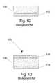
- FIGS. 1A-1Ddepict the fabrication of a simple chalcogenide memory element 100 .
- the basic structure of a chalcogenide memory elementincludes a first electrode, a second electrode and a chalcogenide material interposed between the first and second electrodes. Additional detail of chalcogenide memory devices, as well as examples of variations on the basic structure of a chalcogenide memory element, are given in U.S. Pat. No. 5,998,244 issued Dec. 7, 1999 to Wolstenholme et al., U.S. Pat. No. 5,920,788 issued Jul.
- Chalcogenide memory elementstypically store a single bit, e.g., a low resistivity (high conductivity) corresponding to a first logic state and a high resistivity (low conductivity) corresponding to a second logic state. Differing levels of resistivity of the chalcogenide memory elements are sensed using current sensing techniques well known in the art while applying a read potential of less than the threshold potential.
- Chalcogenide memory elementscan be electrically switched between conductivity states by applying varying electrical fields to the doped chalcogenide material.
- a programming potential above some threshold potentialthe metal dopant atoms are believed to align in a dendritic structure, thereby forming conductive channels and decreasing the resistivity of the chalcogenide material.
- This transitionis reversible by applying a potential having an opposite polarity.
- a range of applied potentials having a magnitude of less than the threshold potential, i.e., read potentialscan be applied without altering the resistivity of the doped chalcogenide materials.
- These read potentialscan be applied to the chalcogenide memory elements for sensing the resistivity of the doped chalcogenide material and, thus, the memory elements' data values.
- a first electrode 110is formed and a chalcogenide layer 115 is formed overlying the first electrode 110 .
- electrical characteristics of chalcogenide layer 115may be improved through doping of the chalcogenide material with metal. This is typically carried out through a process known as photo-doping where diffusion of metal atoms is photon induced.
- a metal layer 120is first formed on the chalcogenide layer 115 as shown in FIG. 1 A.
- the metal layer 120typically contains the copper, silver, gold, aluminum or other high-diffusing metal. Formation of the first electrode 110 and/or the metal layer 120 is typically performed in a vacuum chamber, e.g., using a vacuum sputtering process.
- electromagnetic radiation 125is directed at the metal layer 120 , resulting in diffusion of metal atoms from the metal layer 120 into the chalcogenide layer 115 .
- the electromagnetic radiation 125is generally ultraviolet (UV) light.
- Driving metal atoms into the chalcogenide layer 115results in a doped chalcogenide layer 130 containing the chalcogenide material and the diffused metal.
- the semiconductor wafermust generally be removed from the vacuum chamber to expose the wafer surface to the UV light source.
- the photo-doping processis generally carried out until the metal layer 120 is completely diffused into the doped chalcogenide layer 130 as shown in FIG. 1 C.
- the thickness of the metal layer 120should be chosen such that the desired doping level can be attained in the doped chalcogenide layer 130 .
- the metal layer 120must be thin enough, e.g., hundreds of angstroms, to allow transmission of the electromagnetic radiation 125 in order to produce the desired photon-induced diffusion of metal.
- a second electrode 150is then formed overlying the doped chalcogenide layer 130 and any remaining portion of the metal layer 120 to produce chalcogenide memory element 100 .
- the second electrode 150is preferably a material having a different work function ( ⁇ m ) than the first electrode 110 .
- the work functionis a measure of the energy required to remove an electron from a material's surface.
- the methodsinclude using a plasma to induce diffusion of metal into a chalcogenide layer concurrently with metal deposition.
- the plasmacontains at least one noble gas of low atomic weight, such as neon or helium.
- the plasmahas a sputter yield sufficient to sputter a metal target and a UV component of its emitted spectrum sufficient to induce diffusion of the sputtered metal into the chalcogenide layer.
- a conductive layercan be formed on the doped chalcogenide layer in situ.
- doping of a chalcogenide layer concurrently with metal deposition and formation of a conductive layer in situ with the doping of the chalcogenide layerreduces contamination concerns and physical damage resulting from moving the device substrate from tool to tool, thus facilitating improved device reliability.
- the inventionprovides a method of forming a doped chalcogenide layer.
- the methodincludes sputtering metal using a plasma containing at least one component gas selected from the group consisting of neon and helium and driving the sputtered metal into a layer of chalcogenide material using the UV component generated by the plasma.
- the inventionprovides a method of forming a doped chalcogenide layer.
- the methodincludes forming a layer of chalcogenide material and sputtering metal onto the layer of chalcogenide material using a plasma containing at least two noble gases.
- the plasmaemits a spectrum having a UV component capable of driving the sputtered metal into the layer of chalcogenide material through UV-enhanced diffusion.
- the composition of the plasmais chosen to have an average atomic weight sufficient to produce a desired sputtering efficiency.
- the composition of the plasmais chosen to have a desired relative intensity of a UV component of the emitted spectrum of the plasma.
- the composition of the plasmais chosen to have a desired emitted spectrum of the plasma.
- the inventionprovides a method of forming a chalcogenide memory element having a first electrode, a second electrode, and a doped chalcogenide layer interposed between the first electrode and the second electrode.
- the methodincludes forming a chalcogenide layer on the first electrode, sputtering metal onto the chalcogenide layer and diffusing metal into the chalcogenide layer using a first plasma containing at least one component gas selected from the group consisting of neon and helium, thereby forming the doped chalcogenide layer, and sputtering metal onto the chalcogenide layer using a second plasma containing at least one component gas having an atomic weight higher than an atomic weight of neon, thereby forming the second electrode.
- the first plasma and the second plasmaare the same plasma.
- the composition of the first plasmais modified to generate the second plasma. Such modification of the composition may occur as a step change between sputtering stages or it may occur concurrently with sputtering of the metal.
- the inventionprovides a method of forming a chalcogenide memory element having a first electrode, a second electrode, and a doped chalcogenide layer interposed between the first electrode and the second electrode.
- the methodincludes forming a chalcogenide layer on the first electrode, sputtering silver onto the chalcogenide layer and diffusing silver into the chalcogenide layer using a first plasma generated from feed gas consisting essentially of neon, thereby forming the doped chalcogenide layer, and sputtering silver onto the doped chalcogenide layer using a second plasma generated from feed gas consisting essentially of argon, thereby forming the second electrode.
- the inventionprovides a method of forming a non-volatile memory device.
- the methodincludes forming word lines and forming first electrodes coupled to the word lines, wherein each word line is coupled to more than one first electrode.
- the methodfurther includes forming a chalcogenide layer on each first electrode and sputtering metal onto each chalcogenide layer and diffusing metal into each chalcogenide layer using a first plasma containing at least one component gas selected from the group consisting of neon and helium, thereby forming doped chalcogenide layers.
- the methodstill further includes sputtering metal onto each doped chalcogenide layer using a second, different, plasma, thereby forming second electrodes.
- the second plasmamay contain at least one component gas having an atomic weight higher than the atomic weight of neon.
- the second plasmamay contain nitrogen (N 2 ) such that the second electrode is formed of a metal-nitride material.
- the methodstill further includes forming bit lines coupled to the second electrodes, wherein each bit line is coupled to more than one second electrode.
- Each diodemay be formed interposed between a second electrode and a bit line, such that each second electrode is coupled to a bit line through a diode.
- each diodemay be formed interposed between a first electrode and a word line, such that each first electrode is coupled to a word line through a diode.
- FIGS. 1A-1Dare cross-sectional views of a chalcogenide memory element during various processing stages.
- FIGS. 2A-2Dare cross-sectional views of a chalcogenide memory element during various processing stages in accordance with an embodiment of the invention.
- FIG. 3is a schematic illustration of one physical vapor deposition apparatus suitable for use with the embodiments of the invention.
- FIG. 4is a schematic of a portion of a memory array in accordance with an embodiment of the invention.
- FIG. 5is a simplified block diagram of an integrated circuit memory device in accordance with an embodiment of the invention.
- Examplesinclude silicon-on-sapphire (SOS) technology, silicon-on-insulator (SOI) technology, thin film transistor (TFT) technology, doped and undoped semiconductors, epitaxial layers of a silicon supported by a base semiconductor structure, as well as other semiconductor structures well known to one skilled in the art.
- SOSsilicon-on-sapphire
- SOIsilicon-on-insulator
- TFTthin film transistor
- doped and undoped semiconductorsepitaxial layers of a silicon supported by a base semiconductor structure, as well as other semiconductor structures well known to one skilled in the art.
- wafer and substrateinclude the underlying layers containing such regions/junctions.
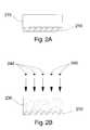
- FIGS. 2A-2Ddepict fabrication of a chalcogenide memory element 200 as a portion of an integrated circuit device in accordance with one embodiment of the invention.
- FIGS. 2A-2Dare cross-sectional views taken during various processing stages.
- a lower or first electrode 210is formed on a substrate (not shown).
- the first electrode 210contains conductive material. Examples include conductively doped polysilicon, carbon (C), metals, metal alloys, metal silicides, conductive metal nitrides and conductive metal oxides.
- the first electrode 210may further contain more than one conductive material.
- the first electrode 210may contain a layer of carbon overlying a layer of molybdenum (Mo) or a layer of tungsten (W) overlying a layer of titanium nitride (TiN).
- the first electrode 210may include one or more adhesion or barrier layers adjacent underlying or overlying layers. Any adhesion or barrier layer should preferably be conductive as to not interfere with programming of the chalcogenide memory element 200 .
- the first electrode 210contains silver.
- the first electrode 210is a layer of silver.
- the first electrode 210is preferably formed using a physical vapor deposition (PVD) process.
- PVDphysical vapor deposition
- Examplesinclude vacuum or thermal evaporation, electron-beam evaporation and sputtering techniques well known in the art.
- PVDphysical vapor deposition
- a source or target containing the material to be depositedis evaporated and may include ionization of some or all of the vaporized target material.
- the vaporized and/or ionized species impinging on the substratecan then deposit on the substrate.
- PVD processesare preferred for their general ability to form layers of high purity, limited only by the purity of the source or target used in the PVD process.
- other deposition techniquesmay be used, such as a chemical vapor deposition (CVD) process in which vaporized chemical precursors are adsorbed on the substrate surface and reacted to form the first electrode 210 .
- CVDchemical vapor deposition
- the first electrode 210has a thickness of approximately 500-1000 ⁇ .
- the first electrode 210has a thickness of approximately 700 ⁇ .
- a chalcogenide layer 215is formed on the first electrode 210 .
- the chalcogenide layer 215is preferably formed using a PVD process, but may be formed using other deposition techniques.
- the chalcogenide layer 215contains a chalcogenide material containing one or more Group VIB elements of the traditional IUPAC version of the periodic table, i.e., oxygen (O), sulfur (S), selenium (Se), tellurium (Te) and polonium (Po), and one or more Groups IVB and VB elements of the traditional IUPAC version of the periodic table, i.e., carbon (C), silicon (Si), germanium (Ge), tin (Sn), lead (Pb), nitrogen (N), phosphorus (P), arsenic (As), antimony (Sb) and bismuth (Bi).
- Group VIB elements of the traditional IUPAC version of the periodic tablei.e., oxygen (O), sulfur (S), selenium (Se), tellurium (Te) and polonium (Po)
- Groups IVB and VB elements of the traditional IUPAC version of the periodic tablei.e., carbon (C), silicon (Si
- the chalcogenide layer 215contains a chalcogenide material containing a combination of selenium and/or tellurium with germanium and/or antimony.
- the chalcogenide layer 215contains a germanium selenide material (GeSe or GeSe 2 ).
- the chalcogenide layer 215has a thickness of approximately 300-700 ⁇ .
- the chalcogenide layer 215has a thickness of approximately 500 ⁇ .
- the chalcogenide layer 215is doped with metal 240 using a sputtering process to produce a doped chalcogenide layer 230 .
- the doped chalcogenide layer 230is doped to a desired doping level.
- the desired doping levelproduces a doped chalcogenide layer 230 saturated with the metal 240 .
- the desired doping levelproduces an oversaturated doped chalcogenide layer 230 .
- the desired doping levelis approximately 15-30 wt % of the metal 240 in the doped chalcogenide layer 230 .
- One example of an apparatus for performing sputteringmay include an ENDURA® system commercially available from Applied Materials, Santa Clara, Calif., USA.
- the plasma generated in such equipmentwill emit a UV component, thus providing photon-induced diffusion during the sputtering process.
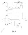
- FIG. 3is a schematic illustration of one PVD apparatus 310 suitable for use with the embodiments of the invention. Those familiar with PVD apparatus will recognize that it is a simplified schematic and that typical PVD apparatus may contain additional or alternate components.
- a conductive pedestal 314 containing substrate 312is located in a deposition chamber 316 .
- the pedestal 314is connected to a DC power source 324 .
- a gas inlet 318is provided for introduction of component gases into the chamber 316 .
- the component gasesmake up the plasma 322 .
- the component gasesare generally fed to the deposition chamber 316 continuously during the operation of the apparatus 310 .
- component gasesdo not include any vaporized target material created during the sputter process.
- a sputter target 326 connected to a DC power source 328is located in the chamber 316 .
- the target 326may be a plate formed of the material to be sputtered.
- materials to be sputtered in the doping of the chalcogenide layer 215include high-diffusion metals such as copper, silver, gold and aluminum. Excess or spent gases are drawn from the deposition chamber 316 through a vent 329 by a vacuum pump (not shown).
- magnets 327aid in the development of the plasma 322 .
- the plasma 322is formed by the application of a bias across the target 326 as a cathode and the substrate 312 as an anode. Magnets 327 are often placed behind the target 326 .
- the plasmais formed at least in part using neon (Ne) and/or helium (He).
- the plasmamay further contain other component gases.
- argon (Ar)which is commonly used in sputtering processes. While argon's spectrum has a UV component as well, its relative intensity is relatively low compared to that of neon or helium, thus resulting in lower rates of metal diffusion.
- the plasma used during the doping processis generated from feed gas consisting essentially of neon.
- the plasma used during the doping processcontains helium.
- the plasma used during the doping processcontains at least argon and neon.
- the plasmacould also be generated from feed gas consisting essentially of helium for its increased UV component, but such use can lead to undesirable reductions in sputtering efficiency.
- feed gasconsisting essentially of helium for its increased UV component, but such use can lead to undesirable reductions in sputtering efficiency.
- Use of lower atomic weight gasescan result in much higher operating pressures than traditional PVD processes, e.g., 30-300 mTorr.
- a plasmaBy adjusting the volume percentages of the gases used in generating the plasma, a plasma can be generated having an average atomic weight anywhere between the lowest atomic weight of the gases and the highest atomic weight of the gases. In this manner, a plasma can be created having an average atomic weight sufficient to facilitate a desired sputtering efficiency.
- Sputtering efficiencygenerally refers to the number of target atoms ejected per incident ion, typically in the range of about 0.5-1.5. Sputtering efficiency largely determines the rate of sputter implantation or deposition. Sputtering efficiency depends on a number of factors, including the direction of incident ions, target material, mass of bombarding ions, the energy of the bombarding ions, dose, crystal state and surface binding energy.
- a plasmaBy adjusting the volume percentages of the gases in the plasma, a plasma also can be generated having a UV component that is a composite of the spectra of the individual gases and having a relative intensity generally between that of the lowest relative intensity of the gases in the plasma and that of the highest relative intensity of the gases in the plasma. In this manner, a plasma can be created having a relative intensity of its composite UV component sufficient to produce a desired level of photon-induced diffusion of the sputtered metal. It is noted that where more than two gases make up the plasma, multiple combinations of these gases can emit UV components having the same relative intensity.
- a plasma having a desired relative intensity of its emitted UV component and a desired average atomic weightthrough the selection of two or more component gases and their relative volume percentages.
- these valuesi.e., the desired relative intensity and the desired average atomic weight
- attaining one valuemay require a compromise on the other.
- One method of compromisewould be to determine the combinations of component gases producing a plasma having the desired relative intensity and then to choose one of these combinations of the component gases having an average atomic weight near the desired atomic weight.
- Another methodwould be to determine the combinations of component gases producing a plasma having the desired average atomic weight and then to choose one of these combinations of the component gases having a relative intensity of its UV component near the desired relative intensity.
- the UV components of differing plasmasmay have differing spectra, but the same relative intensity. Because the spectrum can also affect diffusion rates, it may be desirable to produce a specific emitted spectrum in a resulting plasma. Accordingly, for one embodiment, a mixture of component gases is chosen to produce a desired spectrum of the resulting plasma. For a further embodiment, a mixture of component gases is chosen to produce a desired spectrum of the resulting plasma having a higher level of visible components than a plasma consisting of neon. For another embodiment, a mixture of component gases capable of producing a desired spectrum in a resulting plasma is chosen to produce a target sputter efficiency. In general, the component gases of the plasma used in the sputtering process for doping of the chalcogenide layer 215 are selected to produce desired diffusion and sputtering rates.
- a top or second electrode 250is formed on the doped chalcogenide layer 230 .
- the second electrode 250generally follows the same guidelines as the first electrode 210 . Accordingly, the second electrode 250 contains conductive material. Examples include conductively doped polysilicon, carbon, metals (including refractory metals), metal alloys, metal silicides, conductive metal nitrides and conductive metal oxides.
- the second electrode 250may further contain more than one conductive material.
- the second electrode 250may include one or more adhesion or barrier layers adjacent underlying or overlying layers. Any adhesion or barrier layer should preferably be conductive as to not interfere with programming of the chalcogenide memory element 200 .
- the second electrode 250contains silver.
- the second electrode 250is a layer of silver.
- the second electrode 250is preferably formed using a PVD process, but may be formed by other methods such as CVD techniques.
- the second electrode 250is more preferably formed using the same PVD apparatus and target as used during the doping of the chalcogenide layer 215 . In this manner, the second electrode 250 may be formed in situ with the doping process, thus further reducing risks of contamination or damage associated with transport of the semiconductor substrate. Accordingly, for one embodiment, the second electrode 250 is formed by sputtering metal 245 onto the doped chalcogenide layer 230 .
- the second electrode 250has a thickness of approximately 800-1200 ⁇ .
- the second electrode 250has a thickness of approximately 1000 ⁇ .
- the component gases used during doping of the chalcogenide layer 215are evacuated from the deposition chamber 316 prior to formation of the second electrode 250 .
- a new plasma 322is formed with the new component gases for the deposition of the second electrode 250 .
- doping of the chalcogenide layer 215can be performed using a plasma 322 generated using a feed gas consisting essentially of neon.
- the deposition chamber 316is evacuated after the desired doping level is attained.
- formation of the second electrodecan be performed using a plasma 322 generated using a feed gas consisting essentially of argon.
- the second plasma 322may contain nitrogen or oxygen to form conductive metal nitrides or metal oxides, respectively.
- the component gas feed compositioncould be changed without an evacuation of the deposition chamber 316 .
- doping of the chalcogenide layer 215can be performed using a component gas and plasma 322 having a first composition, e.g., consisting essentially of neon.
- the component gas feedcould be changed to the second composition, e.g., consisting essentially of argon.
- the concentration of argon in the plasma 322will thus gradually increase as argon is fed to the deposition chamber 316 and mixed gases are drawn off.
- the composition of the plasma 322changes, driving to a higher average atomic weight and/or a lower UV component, the dynamics would shift away from diffusion and toward deposition.
- the component gas feed compositioncould be changed gradually instead of making a step change.
- the processing described with reference to FIGS. 2B and 2Ccould be combined using a single composition for plasma 322 .
- the component gasesare chosen such that a desired combination of diffusion and deposition occurs.
- the rate of diffusionshould be high enough relative to the rate of deposition that sufficient doping occurs before the second electrode 250 becomes thick enough to block further diffusion of metal into the doped chalcogenide layer 230 .
- FIG. 2Dshows the chalcogenide memory element 200 upon formation of the second electrode 250 .
- the chalcogenide memory element 200has a doped chalcogenide layer interposed between the first electrode 210 and the second electrode 250 .
- the chalcogenide memory element 200can be used to form a chalcogenide memory cell where the state of the doped chalcogenide layer 230 is indicative of the data value stored by the memory cell.
- FIG. 4is a schematic showing a portion of a memory array 400 containing chalcogenide memory elements 200 as described herein.
- the memory array 400includes a number of memory cells 405 arranged generally in rows and columns. Typical memory arrays 400 contain millions of these memory cells 405 .
- Each memory cell 405includes a chalcogenide memory element 200 coupled between a first conductive line, such as word line 410 , and a diode 415 .
- the diode 415is further coupled between a second conductive line, such as bit line 420 , and the chalcogenide memory element 200 .
- the diode 415could be coupled between the first conductive line and the chalcogenide memory element 200 .
- the diode 415serves as the access device to the memory cell 300 .
- a grouping of memory cells 300 coupled to the same word line 410are typically referred to as a row of memory cells.
- a grouping of memory cells 300 coupled to the same bit line 420are typically referred to as a column of memory cells.
- FIG. 5is a simplified block diagram of an integrated circuit memory device 500 in accordance with an embodiment of the invention.
- the memory device 500is a non-volatile memory device containing chalcogenide memory elements in accordance with the invention.
- the memory device 500includes an array of memory cells 502 including the non-volatile chalcogenide memory elements.
- the memory array 502is arranged in a plurality of addressable banks. In one embodiment, the memory contains four memory banks 504 , 506 , 508 and 510 . Each memory bank contains addressable rows and columns of memory cells.
- the data stored in the memory array 502can be accessed using externally provided location addresses received by address register 512 via address signal connections 528 .
- the addressesare decoded using bank decode logic 516 to select a target memory bank.
- the addressesare also decoded using row decode circuitry 514 to select the target rows.
- the addressesare further decoded using column decode circuitry 518 to select one or more target columns.
- I/O circuit 528includes data output registers, output drivers and output buffers.
- Command execution logic 522is provided to control the basic operations of the memory device 500 in response to control signals received via control signal connections 526 .
- a state machine 524may also be provided to control specific operations performed on the memory array and cells.
- the command execution logic 522 and/or state machine 524can be generally referred to as control circuitry to control read, write, erase and other memory operations.
- the data connections 530are typically used for bi-directional data communication.
- the memorycan be coupled to an external processor 550 for operation or testing.
- FIG. 5has been simplified to help focus on the invention. It will be understood that the above description of a memory device is intended to provide a general understanding of the memory and is not a complete description of all the elements and features of a typical memory device.
- memory devices of the type described hereinare generally fabricated as an integrated circuit containing a variety of semiconductor devices.
- the integrated circuitis supported by a substrate.
- Integrated circuitsare typically repeated multiple times on each substrate.
- the substrateis further processed to separate the integrated circuits into dies as is well known in the art.
- the methodsinclude using a plasma to induce diffusion of metal into a chalcogenide layer concurrently with metal deposition.
- the plasmacontains at least one noble gas of low atomic weight, such as neon or helium.
- the plasmahas a sputter yield sufficient to sputter a metal target and a UV component of its emitted spectrum sufficient to induce diffusion of the sputtered metal into the chalcogenide layer.
- a conductive layercan be formed on the doped chalcogenide layer in situ.
- doping of a chalcogenide layer concurrently with metal deposition and formation of a conductive layer in situ with the doping of the chalcogenide layerreduces contamination concerns and physical damage resulting from moving the device substrate from tool to tool, thus facilitating improved device reliability.
Landscapes
- Chemical & Material Sciences (AREA)
- Engineering & Computer Science (AREA)
- Chemical Kinetics & Catalysis (AREA)
- Materials Engineering (AREA)
- Mechanical Engineering (AREA)
- Metallurgy (AREA)
- Organic Chemistry (AREA)
- Manufacturing & Machinery (AREA)
- Inorganic Chemistry (AREA)
- Semiconductor Memories (AREA)
- Physical Vapour Deposition (AREA)
- Inks, Pencil-Leads, Or Crayons (AREA)
Abstract
Description
Claims (26)
Priority Applications (14)
| Application Number | Priority Date | Filing Date | Title |
|---|---|---|---|
| US09/943,426US6709958B2 (en) | 2001-08-30 | 2001-08-30 | Integrated circuit device and fabrication using metal-doped chalcogenide materials |
| PCT/US2002/027526WO2003020998A2 (en) | 2001-08-30 | 2002-08-30 | Integrated circuit device and fabrication using metal-doped chalcogenide materials |
| EP07006928AEP1801898B1 (en) | 2001-08-30 | 2002-08-30 | Integrated circuit device and fabrication using metal-doped chalcogenide materials |
| EP02766168AEP1425431B1 (en) | 2001-08-30 | 2002-08-30 | Integrated circuit device and fabrication using metal-doped chalcogenide materials |
| AT02766168TATE422560T1 (en) | 2001-08-30 | 2002-08-30 | INTEGRATED CIRCUIT ELEMENT AND MANUFACTURE WITH METAL-DOPED CHALCOGENIDE MATERIALS |
| JP2003525695AJP4194490B2 (en) | 2001-08-30 | 2002-08-30 | Integrated circuit devices and fabrication using metal doped chalcogenide materials |
| CNB2007100854187ACN100550460C (en) | 2001-08-30 | 2002-08-30 | Utilize the integrated circuit (IC)-components and the manufacturing of the chalcogenide material behind the doping metals |
| KR1020047003083AKR100586716B1 (en) | 2001-08-30 | 2002-08-30 | Doped chalcogenide layer formation method, chalcogenide memory device formation method and nonvolatile memory device formation method |
| DE60231129TDE60231129D1 (en) | 2001-08-30 | 2002-08-30 | INTEGRATED CIRCUIT ELEMENT AND MANUFACTURE WITH METAL-DOTTED CHALKOGENIDE MATERIALS |
| AT07006928TATE529540T1 (en) | 2001-08-30 | 2002-08-30 | INTEGRATED CIRCUIT DEVICE AND FABRICATION USING METAL-DOPED CHALCOGENIDE MATERIALS |
| CNB028214501ACN100402694C (en) | 2001-08-30 | 2002-08-30 | Integrated circuit devices and fabrication using metal-doped chalcogenide materials |
| US10/285,462US6730547B2 (en) | 2001-08-30 | 2002-11-01 | Integrated circuit device and fabrication using metal-doped chalcogenide materials |
| US10/285,463US6800504B2 (en) | 2001-08-30 | 2002-11-01 | Integrated circuit device and fabrication using metal-doped chalcogenide materials |
| US10/872,773US20050026433A1 (en) | 2001-08-30 | 2004-06-22 | Integrated circuit device and fabrication using metal-doped chalcogenide materials |
Applications Claiming Priority (1)
| Application Number | Priority Date | Filing Date | Title |
|---|---|---|---|
| US09/943,426US6709958B2 (en) | 2001-08-30 | 2001-08-30 | Integrated circuit device and fabrication using metal-doped chalcogenide materials |
Related Child Applications (2)
| Application Number | Title | Priority Date | Filing Date |
|---|---|---|---|
| US10/285,463DivisionUS6800504B2 (en) | 2001-08-30 | 2002-11-01 | Integrated circuit device and fabrication using metal-doped chalcogenide materials |
| US10/285,462DivisionUS6730547B2 (en) | 2001-08-30 | 2002-11-01 | Integrated circuit device and fabrication using metal-doped chalcogenide materials |
Publications (2)
| Publication Number | Publication Date |
|---|---|
| US20030186504A1 US20030186504A1 (en) | 2003-10-02 |
| US6709958B2true US6709958B2 (en) | 2004-03-23 |
Family
ID=25479641
Family Applications (4)
| Application Number | Title | Priority Date | Filing Date |
|---|---|---|---|
| US09/943,426Expired - LifetimeUS6709958B2 (en) | 2001-08-30 | 2001-08-30 | Integrated circuit device and fabrication using metal-doped chalcogenide materials |
| US10/285,463Expired - LifetimeUS6800504B2 (en) | 2001-08-30 | 2002-11-01 | Integrated circuit device and fabrication using metal-doped chalcogenide materials |
| US10/285,462Expired - LifetimeUS6730547B2 (en) | 2001-08-30 | 2002-11-01 | Integrated circuit device and fabrication using metal-doped chalcogenide materials |
| US10/872,773AbandonedUS20050026433A1 (en) | 2001-08-30 | 2004-06-22 | Integrated circuit device and fabrication using metal-doped chalcogenide materials |
Family Applications After (3)
| Application Number | Title | Priority Date | Filing Date |
|---|---|---|---|
| US10/285,463Expired - LifetimeUS6800504B2 (en) | 2001-08-30 | 2002-11-01 | Integrated circuit device and fabrication using metal-doped chalcogenide materials |
| US10/285,462Expired - LifetimeUS6730547B2 (en) | 2001-08-30 | 2002-11-01 | Integrated circuit device and fabrication using metal-doped chalcogenide materials |
| US10/872,773AbandonedUS20050026433A1 (en) | 2001-08-30 | 2004-06-22 | Integrated circuit device and fabrication using metal-doped chalcogenide materials |
Country Status (8)
| Country | Link |
|---|---|
| US (4) | US6709958B2 (en) |
| EP (2) | EP1801898B1 (en) |
| JP (1) | JP4194490B2 (en) |
| KR (1) | KR100586716B1 (en) |
| CN (2) | CN100550460C (en) |
| AT (2) | ATE529540T1 (en) |
| DE (1) | DE60231129D1 (en) |
| WO (1) | WO2003020998A2 (en) |
Cited By (27)
| Publication number | Priority date | Publication date | Assignee | Title |
|---|---|---|---|---|
| US20030052330A1 (en)* | 2001-09-20 | 2003-03-20 | Klein Rita J. | Electro-and electroless plating of metal in the manufacture of PCRAM devices |
| US20030173558A1 (en)* | 2002-03-14 | 2003-09-18 | Campbell Kristy A. | Methods and apparatus for resistance variable material cells |
| US20040115938A1 (en)* | 2001-04-12 | 2004-06-17 | Roland Scheer | Method for producing a chalcogenide-semiconductor layer of the abc2 type with optical process monitoring |
| US20050027409A1 (en)* | 2002-12-31 | 2005-02-03 | Bae Systems Information And Electronic Systems Integration, Inc. | Use of radiation-hardened chalcogenide technology for spaceborne reconfigurable digital processing systems |
| US20050026433A1 (en)* | 2001-08-30 | 2005-02-03 | Jiutao Li | Integrated circuit device and fabrication using metal-doped chalcogenide materials |
| US20050250281A1 (en)* | 2004-04-26 | 2005-11-10 | Infineon Technologies Ag | Method for manufacturing resistively switching memory devices |
| US20050287698A1 (en)* | 2004-06-28 | 2005-12-29 | Zhiyong Li | Use of chalcogen plasma to form chalcogenide switching materials for nanoscale electronic devices |
| US20060044878A1 (en)* | 2004-09-02 | 2006-03-02 | Perner Frederick A | Programming of programmable resistive memory devices |
| US20060097775A1 (en)* | 2004-11-11 | 2006-05-11 | International Business Machines Corporation | Circuit and Method of Controlling Integrated Circuit Power Consumption Using Phase Change Switches |
| US20060240663A1 (en)* | 2004-12-03 | 2006-10-26 | Mcteer Allen | Methods of forming a resistance variable element |
| US20070007505A1 (en)* | 2005-07-07 | 2007-01-11 | Honeywell International Inc. | Chalcogenide PVD components |
| US20070007579A1 (en)* | 2005-07-11 | 2007-01-11 | Matrix Semiconductor, Inc. | Memory cell comprising a thin film three-terminal switching device having a metal source and /or drain region |
| US20070080428A1 (en)* | 2005-10-12 | 2007-04-12 | Herman Gregory S | Semiconductor film composition |
| US20070212893A1 (en)* | 2006-03-07 | 2007-09-13 | Mcteer Allen | System and method for sputtering a tensile silicon nitride film |
| US20070287252A1 (en)* | 2006-06-09 | 2007-12-13 | Micron Technology, Inc. | Methods of forming variable resistance memory cells, and methods of etching germanium, antimony, and tellurium-comprising materials |
| US20070291533A1 (en)* | 2006-06-16 | 2007-12-20 | Industrial Technology Research Institute | Phase change memory device and fabrication method thereof |
| US20080062736A1 (en)* | 2002-02-01 | 2008-03-13 | Hitachi, Ltd. | Storage device |
| US20090093083A1 (en)* | 2006-06-29 | 2009-04-09 | Yu-Min Jung | Method of depositing chalcogenide film for phase-change memory |
| US20090233421A1 (en)* | 2008-03-17 | 2009-09-17 | Samsung Electronics Co., Ltd, | Methods of Fabricating Semiconductor Device Including Phase Change Layer |
| US20100044698A1 (en)* | 2005-10-12 | 2010-02-25 | Gregory Herman | Semiconductor Film Composition |
| US9245742B2 (en) | 2013-12-18 | 2016-01-26 | Asm Ip Holding B.V. | Sulfur-containing thin films |
| US9461134B1 (en) | 2015-05-20 | 2016-10-04 | Asm Ip Holding B.V. | Method for forming source/drain contact structure with chalcogen passivation |
| US9478419B2 (en) | 2013-12-18 | 2016-10-25 | Asm Ip Holding B.V. | Sulfur-containing thin films |
| US9711350B2 (en) | 2015-06-03 | 2017-07-18 | Asm Ip Holding B.V. | Methods for semiconductor passivation by nitridation |
| US9711396B2 (en) | 2015-06-16 | 2017-07-18 | Asm Ip Holding B.V. | Method for forming metal chalcogenide thin films on a semiconductor device |
| US9741815B2 (en) | 2015-06-16 | 2017-08-22 | Asm Ip Holding B.V. | Metal selenide and metal telluride thin films for semiconductor device applications |
| US10490475B2 (en) | 2015-06-03 | 2019-11-26 | Asm Ip Holding B.V. | Methods for semiconductor passivation by nitridation after oxide removal |
Families Citing this family (254)
| Publication number | Priority date | Publication date | Assignee | Title |
|---|---|---|---|---|
| US6542690B1 (en)* | 2000-05-08 | 2003-04-01 | Corning Incorporated | Chalcogenide doping of oxide glasses |
| JP4742429B2 (en)* | 2001-02-19 | 2011-08-10 | 住友電気工業株式会社 | Method for producing glass particulate deposit |
| US6734455B2 (en)* | 2001-03-15 | 2004-05-11 | Micron Technology, Inc. | Agglomeration elimination for metal sputter deposition of chalcogenides |
| US7102150B2 (en)* | 2001-05-11 | 2006-09-05 | Harshfield Steven T | PCRAM memory cell and method of making same |
| US6951805B2 (en)* | 2001-08-01 | 2005-10-04 | Micron Technology, Inc. | Method of forming integrated circuitry, method of forming memory circuitry, and method of forming random access memory circuitry |
| US6784018B2 (en)* | 2001-08-29 | 2004-08-31 | Micron Technology, Inc. | Method of forming chalcogenide comprising devices and method of forming a programmable memory cell of memory circuitry |
| US6881623B2 (en) | 2001-08-29 | 2005-04-19 | Micron Technology, Inc. | Method of forming chalcogenide comprising devices, method of forming a programmable memory cell of memory circuitry, and a chalcogenide comprising device |
| US6955940B2 (en)* | 2001-08-29 | 2005-10-18 | Micron Technology, Inc. | Method of forming chalcogenide comprising devices |
| US6646902B2 (en) | 2001-08-30 | 2003-11-11 | Micron Technology, Inc. | Method of retaining memory state in a programmable conductor RAM |
| US6612695B2 (en)* | 2001-11-07 | 2003-09-02 | Michael Waters | Lighted reading glasses |
| US6815818B2 (en)* | 2001-11-19 | 2004-11-09 | Micron Technology, Inc. | Electrode structure for use in an integrated circuit |
| US6791859B2 (en) | 2001-11-20 | 2004-09-14 | Micron Technology, Inc. | Complementary bit PCRAM sense amplifier and method of operation |
| US6909656B2 (en)* | 2002-01-04 | 2005-06-21 | Micron Technology, Inc. | PCRAM rewrite prevention |
| US6867064B2 (en)* | 2002-02-15 | 2005-03-15 | Micron Technology, Inc. | Method to alter chalcogenide glass for improved switching characteristics |
| US6791885B2 (en)* | 2002-02-19 | 2004-09-14 | Micron Technology, Inc. | Programmable conductor random access memory and method for sensing same |
| US7087919B2 (en)* | 2002-02-20 | 2006-08-08 | Micron Technology, Inc. | Layered resistance variable memory device and method of fabrication |
| US6847535B2 (en) | 2002-02-20 | 2005-01-25 | Micron Technology, Inc. | Removable programmable conductor memory card and associated read/write device and method of operation |
| US6809362B2 (en)* | 2002-02-20 | 2004-10-26 | Micron Technology, Inc. | Multiple data state memory cell |
| US7151273B2 (en)* | 2002-02-20 | 2006-12-19 | Micron Technology, Inc. | Silver-selenide/chalcogenide glass stack for resistance variable memory |
| US6937528B2 (en)* | 2002-03-05 | 2005-08-30 | Micron Technology, Inc. | Variable resistance memory and method for sensing same |
| US6864500B2 (en)* | 2002-04-10 | 2005-03-08 | Micron Technology, Inc. | Programmable conductor memory cell structure |
| US6855975B2 (en)* | 2002-04-10 | 2005-02-15 | Micron Technology, Inc. | Thin film diode integrated with chalcogenide memory cell |
| US6858482B2 (en)* | 2002-04-10 | 2005-02-22 | Micron Technology, Inc. | Method of manufacture of programmable switching circuits and memory cells employing a glass layer |
| US20030205822A1 (en)* | 2002-05-02 | 2003-11-06 | Taiwan Semiconductor Manufacturing Co. Ltd. | Low-strength plasma treatment for interconnects |
| US6731528B2 (en)* | 2002-05-03 | 2004-05-04 | Micron Technology, Inc. | Dual write cycle programmable conductor memory system and method of operation |
| US6890790B2 (en)* | 2002-06-06 | 2005-05-10 | Micron Technology, Inc. | Co-sputter deposition of metal-doped chalcogenides |
| US6825135B2 (en)* | 2002-06-06 | 2004-11-30 | Micron Technology, Inc. | Elimination of dendrite formation during metal/chalcogenide glass deposition |
| US7209378B2 (en)* | 2002-08-08 | 2007-04-24 | Micron Technology, Inc. | Columnar 1T-N memory cell structure |
| US7018863B2 (en)* | 2002-08-22 | 2006-03-28 | Micron Technology, Inc. | Method of manufacture of a resistance variable memory cell |
| US6831019B1 (en)* | 2002-08-29 | 2004-12-14 | Micron Technology, Inc. | Plasma etching methods and methods of forming memory devices comprising a chalcogenide comprising layer received operably proximate conductive electrodes |
| US7294527B2 (en) | 2002-08-29 | 2007-11-13 | Micron Technology Inc. | Method of forming a memory cell |
| US7364644B2 (en)* | 2002-08-29 | 2008-04-29 | Micron Technology, Inc. | Silver selenide film stoichiometry and morphology control in sputter deposition |
| US6867114B2 (en)* | 2002-08-29 | 2005-03-15 | Micron Technology Inc. | Methods to form a memory cell with metal-rich metal chalcogenide |
| US6864521B2 (en)* | 2002-08-29 | 2005-03-08 | Micron Technology, Inc. | Method to control silver concentration in a resistance variable memory element |
| US7010644B2 (en)* | 2002-08-29 | 2006-03-07 | Micron Technology, Inc. | Software refreshed memory device and method |
| US7163837B2 (en) | 2002-08-29 | 2007-01-16 | Micron Technology, Inc. | Method of forming a resistance variable memory element |
| US7531823B2 (en)* | 2003-01-23 | 2009-05-12 | Nec Corporation | Electron device, integrated electron device using same, and operating method using same |
| US7115927B2 (en) | 2003-02-24 | 2006-10-03 | Samsung Electronics Co., Ltd. | Phase changeable memory devices |
| US7402851B2 (en)* | 2003-02-24 | 2008-07-22 | Samsung Electronics Co., Ltd. | Phase changeable memory devices including nitrogen and/or silicon and methods for fabricating the same |
| US7022579B2 (en)* | 2003-03-14 | 2006-04-04 | Micron Technology, Inc. | Method for filling via with metal |
| US6930909B2 (en) | 2003-06-25 | 2005-08-16 | Micron Technology, Inc. | Memory device and methods of controlling resistance variation and resistance profile drift |
| US6961277B2 (en) | 2003-07-08 | 2005-11-01 | Micron Technology, Inc. | Method of refreshing a PCRAM memory device |
| US7061004B2 (en)* | 2003-07-21 | 2006-06-13 | Micron Technology, Inc. | Resistance variable memory elements and methods of formation |
| US6903361B2 (en) | 2003-09-17 | 2005-06-07 | Micron Technology, Inc. | Non-volatile memory structure |
| US7562375B2 (en)* | 2003-10-10 | 2009-07-14 | Microsoft Corporation | Fast channel change |
| US7583551B2 (en)* | 2004-03-10 | 2009-09-01 | Micron Technology, Inc. | Power management control and controlling memory refresh operations |
| US7098068B2 (en)* | 2004-03-10 | 2006-08-29 | Micron Technology, Inc. | Method of forming a chalcogenide material containing device |
| DE102004029436B4 (en)* | 2004-06-18 | 2009-03-05 | Qimonda Ag | A method of manufacturing a solid electrolyte material region |
| US7354793B2 (en)* | 2004-08-12 | 2008-04-08 | Micron Technology, Inc. | Method of forming a PCRAM device incorporating a resistance-variable chalocogenide element |
| US7326950B2 (en)* | 2004-07-19 | 2008-02-05 | Micron Technology, Inc. | Memory device with switching glass layer |
| US7190048B2 (en)* | 2004-07-19 | 2007-03-13 | Micron Technology, Inc. | Resistance variable memory device and method of fabrication |
| US7365411B2 (en) | 2004-08-12 | 2008-04-29 | Micron Technology, Inc. | Resistance variable memory with temperature tolerant materials |
| US7151688B2 (en)* | 2004-09-01 | 2006-12-19 | Micron Technology, Inc. | Sensing of resistance variable memory devices |
| US20060102870A1 (en)* | 2004-10-20 | 2006-05-18 | Viens Jean F | Infrared detection material and method of production |
| US7608503B2 (en) | 2004-11-22 | 2009-10-27 | Macronix International Co., Ltd. | Side wall active pin memory and manufacturing method |
| US7374174B2 (en)* | 2004-12-22 | 2008-05-20 | Micron Technology, Inc. | Small electrode for resistance variable devices |
| US20060131555A1 (en)* | 2004-12-22 | 2006-06-22 | Micron Technology, Inc. | Resistance variable devices with controllable channels |
| FR2880177B1 (en) | 2004-12-23 | 2007-05-18 | Commissariat Energie Atomique | MEMORY PMC HAVING IMPROVED RETENTION TIME AND WRITING SPEED |
| DE102005001253A1 (en)* | 2005-01-11 | 2006-07-20 | Infineon Technologies Ag | Memory cell arrangement for solid electrolyte memory cells has lower electrode and upper electrode and activated solid electrolyte material area between them as memory material area and whole of material area is coherently designed |
| US20060172067A1 (en)* | 2005-01-28 | 2006-08-03 | Energy Conversion Devices, Inc | Chemical vapor deposition of chalcogenide materials |
| DE102005005325B4 (en)* | 2005-02-04 | 2011-12-15 | Adesto Technology Corp., Inc. | Method for producing a resistively switching non-volatile memory cell |
| US7317200B2 (en) | 2005-02-23 | 2008-01-08 | Micron Technology, Inc. | SnSe-based limited reprogrammable cell |
| DE102005012047A1 (en)* | 2005-03-16 | 2006-09-28 | Infineon Technologies Ag | Solid-state electrolyte memory manufacture involves coating first electrode with solid-state electrolyte layer, and then forming second electrode on solid-state electrolyte layer |
| KR100694188B1 (en)* | 2005-03-22 | 2007-03-14 | 한국표준과학연구원 | Memory and its manufacturing method |
| US7269044B2 (en) | 2005-04-22 | 2007-09-11 | Micron Technology, Inc. | Method and apparatus for accessing a memory array |
| US7709289B2 (en) | 2005-04-22 | 2010-05-04 | Micron Technology, Inc. | Memory elements having patterned electrodes and method of forming the same |
| US7427770B2 (en) | 2005-04-22 | 2008-09-23 | Micron Technology, Inc. | Memory array for increased bit density |
| US7269079B2 (en) | 2005-05-16 | 2007-09-11 | Micron Technology, Inc. | Power circuits for reducing a number of power supply voltage taps required for sensing a resistive memory |
| US7696503B2 (en)* | 2005-06-17 | 2010-04-13 | Macronix International Co., Ltd. | Multi-level memory cell having phase change element and asymmetrical thermal boundary |
| US7238994B2 (en) | 2005-06-17 | 2007-07-03 | Macronix International Co., Ltd. | Thin film plate phase change ram circuit and manufacturing method |
| US7233520B2 (en)* | 2005-07-08 | 2007-06-19 | Micron Technology, Inc. | Process for erasing chalcogenide variable resistance memory bits |
| US7274034B2 (en) | 2005-08-01 | 2007-09-25 | Micron Technology, Inc. | Resistance variable memory device with sputtered metal-chalcogenide region and method of fabrication |
| US7332735B2 (en)* | 2005-08-02 | 2008-02-19 | Micron Technology, Inc. | Phase change memory cell and method of formation |
| US7317567B2 (en)* | 2005-08-02 | 2008-01-08 | Micron Technology, Inc. | Method and apparatus for providing color changing thin film material |
| KR100682969B1 (en)* | 2005-08-04 | 2007-02-15 | 삼성전자주식회사 | Phase change material, phase change ram including the same and method of manufacturing and operating the same |
| US7579615B2 (en)* | 2005-08-09 | 2009-08-25 | Micron Technology, Inc. | Access transistor for memory device |
| US20070037316A1 (en)* | 2005-08-09 | 2007-02-15 | Micron Technology, Inc. | Memory cell contact using spacers |
| US7304368B2 (en)* | 2005-08-11 | 2007-12-04 | Micron Technology, Inc. | Chalcogenide-based electrokinetic memory element and method of forming the same |
| US7251154B2 (en) | 2005-08-15 | 2007-07-31 | Micron Technology, Inc. | Method and apparatus providing a cross-point memory array using a variable resistance memory cell and capacitance |
| KR100637235B1 (en)* | 2005-08-26 | 2006-10-20 | 삼성에스디아이 주식회사 | Plasma display panel |
| US7277313B2 (en)* | 2005-08-31 | 2007-10-02 | Micron Technology, Inc. | Resistance variable memory element with threshold device and method of forming the same |
| KR100694316B1 (en) | 2005-09-30 | 2007-03-14 | 한양대학교 산학협력단 | Method for manufacturing RERRAM device having excellent stability of oxide thin film using plasma gas treatment |
| US7394088B2 (en) | 2005-11-15 | 2008-07-01 | Macronix International Co., Ltd. | Thermally contained/insulated phase change memory device and method (combined) |
| US7635855B2 (en) | 2005-11-15 | 2009-12-22 | Macronix International Co., Ltd. | I-shaped phase change memory cell |
| US7450411B2 (en)* | 2005-11-15 | 2008-11-11 | Macronix International Co., Ltd. | Phase change memory device and manufacturing method |
| US7786460B2 (en) | 2005-11-15 | 2010-08-31 | Macronix International Co., Ltd. | Phase change memory device and manufacturing method |
| US7414258B2 (en) | 2005-11-16 | 2008-08-19 | Macronix International Co., Ltd. | Spacer electrode small pin phase change memory RAM and manufacturing method |
| US7507986B2 (en)* | 2005-11-21 | 2009-03-24 | Macronix International Co., Ltd. | Thermal isolation for an active-sidewall phase change memory cell |
| US7479649B2 (en) | 2005-11-21 | 2009-01-20 | Macronix International Co., Ltd. | Vacuum jacketed electrode for phase change memory element |
| US7829876B2 (en)* | 2005-11-21 | 2010-11-09 | Macronix International Co., Ltd. | Vacuum cell thermal isolation for a phase change memory device |
| US7449710B2 (en) | 2005-11-21 | 2008-11-11 | Macronix International Co., Ltd. | Vacuum jacket for phase change memory element |
| CN100524878C (en) | 2005-11-21 | 2009-08-05 | 旺宏电子股份有限公司 | Programmable resistive material memory array with air-insulated cells |
| US7599217B2 (en)* | 2005-11-22 | 2009-10-06 | Macronix International Co., Ltd. | Memory cell device and manufacturing method |
| US7459717B2 (en) | 2005-11-28 | 2008-12-02 | Macronix International Co., Ltd. | Phase change memory cell and manufacturing method |
| US7688619B2 (en)* | 2005-11-28 | 2010-03-30 | Macronix International Co., Ltd. | Phase change memory cell and manufacturing method |
| US7521364B2 (en)* | 2005-12-02 | 2009-04-21 | Macronix Internation Co., Ltd. | Surface topology improvement method for plug surface areas |
| FR2895531B1 (en)* | 2005-12-23 | 2008-05-09 | Commissariat Energie Atomique | IMPROVED METHOD FOR MAKING MEMORY CELLS OF THE PMC TYPE |
| US7531825B2 (en) | 2005-12-27 | 2009-05-12 | Macronix International Co., Ltd. | Method for forming self-aligned thermal isolation cell for a variable resistance memory array |
| US8062833B2 (en) | 2005-12-30 | 2011-11-22 | Macronix International Co., Ltd. | Chalcogenide layer etching method |
| US7595218B2 (en) | 2006-01-09 | 2009-09-29 | Macronix International Co., Ltd. | Programmable resistive RAM and manufacturing method |
| US7560337B2 (en) | 2006-01-09 | 2009-07-14 | Macronix International Co., Ltd. | Programmable resistive RAM and manufacturing method |
| US7741636B2 (en) | 2006-01-09 | 2010-06-22 | Macronix International Co., Ltd. | Programmable resistive RAM and manufacturing method |
| US7432206B2 (en) | 2006-01-24 | 2008-10-07 | Macronix International Co., Ltd. | Self-aligned manufacturing method, and manufacturing method for thin film fuse phase change ram |
| US7956358B2 (en) | 2006-02-07 | 2011-06-07 | Macronix International Co., Ltd. | I-shaped phase change memory cell with thermal isolation |
| DE102006009254B3 (en)* | 2006-02-28 | 2007-07-12 | Infineon Technologies Ag | Method for producing an integrated electronic circuit with programmable resistive cells, corresponding cells and data memories with such |
| US8492810B2 (en)* | 2006-02-28 | 2013-07-23 | Qimonda Ag | Method of fabricating an integrated electronic circuit with programmable resistance cells |
| US7554144B2 (en) | 2006-04-17 | 2009-06-30 | Macronix International Co., Ltd. | Memory device and manufacturing method |
| US7928421B2 (en)* | 2006-04-21 | 2011-04-19 | Macronix International Co., Ltd. | Phase change memory cell with vacuum spacer |
| KR100782482B1 (en)* | 2006-05-19 | 2007-12-05 | 삼성전자주식회사 | A phase change memory cell employing a thin film as a phase change material film, a phase change memory device having the same, an electronic device having the same, and a manufacturing method thereof |
| US7423300B2 (en)* | 2006-05-24 | 2008-09-09 | Macronix International Co., Ltd. | Single-mask phase change memory element |
| JP5145217B2 (en)* | 2006-05-31 | 2013-02-13 | ルネサスエレクトロニクス株式会社 | Semiconductor device |
| US7696506B2 (en)* | 2006-06-27 | 2010-04-13 | Macronix International Co., Ltd. | Memory cell with memory material insulation and manufacturing method |
| KR100791071B1 (en)* | 2006-07-04 | 2008-01-02 | 삼성전자주식회사 | Programmable device once, electronic system having same and method of operation thereof |
| US7785920B2 (en) | 2006-07-12 | 2010-08-31 | Macronix International Co., Ltd. | Method for making a pillar-type phase change memory element |
| CN100452319C (en)* | 2006-07-14 | 2009-01-14 | 上海华虹Nec电子有限公司 | Making method for silicide damaged by low plasma inducing growth |
| US8115282B2 (en)* | 2006-07-25 | 2012-02-14 | Adesto Technology Corporation | Memory cell device and method of manufacture |
| KR100838527B1 (en) | 2006-07-31 | 2008-06-17 | 삼성전자주식회사 | Phase change memory device formation method |
| US7560723B2 (en)* | 2006-08-29 | 2009-07-14 | Micron Technology, Inc. | Enhanced memory density resistance variable memory cells, arrays, devices and systems including the same, and methods of fabrication |
| US7772581B2 (en) | 2006-09-11 | 2010-08-10 | Macronix International Co., Ltd. | Memory device having wide area phase change element and small electrode contact area |
| KR100829601B1 (en)* | 2006-09-27 | 2008-05-14 | 삼성전자주식회사 | Chalcogen compound target, manufacturing method thereof and manufacturing method of phase change memory device |
| US7504653B2 (en) | 2006-10-04 | 2009-03-17 | Macronix International Co., Ltd. | Memory cell device with circumferentially-extending memory element |
| US7510929B2 (en) | 2006-10-18 | 2009-03-31 | Macronix International Co., Ltd. | Method for making memory cell device |
| US7863655B2 (en) | 2006-10-24 | 2011-01-04 | Macronix International Co., Ltd. | Phase change memory cells with dual access devices |
| US7682868B2 (en)* | 2006-12-06 | 2010-03-23 | Macronix International Co., Ltd. | Method for making a keyhole opening during the manufacture of a memory cell |
| US7473576B2 (en) | 2006-12-06 | 2009-01-06 | Macronix International Co., Ltd. | Method for making a self-converged void and bottom electrode for memory cell |
| US7476587B2 (en) | 2006-12-06 | 2009-01-13 | Macronix International Co., Ltd. | Method for making a self-converged memory material element for memory cell |
| US7903447B2 (en) | 2006-12-13 | 2011-03-08 | Macronix International Co., Ltd. | Method, apparatus and computer program product for read before programming process on programmable resistive memory cell |
| US8344347B2 (en) | 2006-12-15 | 2013-01-01 | Macronix International Co., Ltd. | Multi-layer electrode structure |
| US7718989B2 (en)* | 2006-12-28 | 2010-05-18 | Macronix International Co., Ltd. | Resistor random access memory cell device |
| US7433226B2 (en)* | 2007-01-09 | 2008-10-07 | Macronix International Co., Ltd. | Method, apparatus and computer program product for read before programming process on multiple programmable resistive memory cell |
| US7440315B2 (en)* | 2007-01-09 | 2008-10-21 | Macronix International Co., Ltd. | Method, apparatus and computer program product for stepped reset programming process on programmable resistive memory cell |
| US7535756B2 (en) | 2007-01-31 | 2009-05-19 | Macronix International Co., Ltd. | Method to tighten set distribution for PCRAM |
| US7663135B2 (en) | 2007-01-31 | 2010-02-16 | Macronix International Co., Ltd. | Memory cell having a side electrode contact |
| US7701759B2 (en) | 2007-02-05 | 2010-04-20 | Macronix International Co., Ltd. | Memory cell device and programming methods |
| US7483292B2 (en) | 2007-02-07 | 2009-01-27 | Macronix International Co., Ltd. | Memory cell with separate read and program paths |
| US7463512B2 (en) | 2007-02-08 | 2008-12-09 | Macronix International Co., Ltd. | Memory element with reduced-current phase change element |
| US8138028B2 (en) | 2007-02-12 | 2012-03-20 | Macronix International Co., Ltd | Method for manufacturing a phase change memory device with pillar bottom electrode |
| US7884343B2 (en) | 2007-02-14 | 2011-02-08 | Macronix International Co., Ltd. | Phase change memory cell with filled sidewall memory element and method for fabricating the same |
| KR100888145B1 (en)* | 2007-02-22 | 2009-03-13 | 성균관대학교산학협력단 | Stress-free flexible circuit board manufacturing apparatus and method |
| US7956344B2 (en) | 2007-02-27 | 2011-06-07 | Macronix International Co., Ltd. | Memory cell with memory element contacting ring-shaped upper end of bottom electrode |
| US8268664B2 (en)* | 2007-03-05 | 2012-09-18 | Altis Semiconductor | Methods of manufacturing a semiconductor device; method of manufacturing a memory cell; semiconductor device; semiconductor processing device; integrated circuit having a memory cell |
| US7786461B2 (en) | 2007-04-03 | 2010-08-31 | Macronix International Co., Ltd. | Memory structure with reduced-size memory element between memory material portions |
| US8610098B2 (en)* | 2007-04-06 | 2013-12-17 | Macronix International Co., Ltd. | Phase change memory bridge cell with diode isolation device |
| US7755076B2 (en)* | 2007-04-17 | 2010-07-13 | Macronix International Co., Ltd. | 4F2 self align side wall active phase change memory |
| US7569844B2 (en) | 2007-04-17 | 2009-08-04 | Macronix International Co., Ltd. | Memory cell sidewall contacting side electrode |
| US7483316B2 (en)* | 2007-04-24 | 2009-01-27 | Macronix International Co., Ltd. | Method and apparatus for refreshing programmable resistive memory |
| US8846516B2 (en)* | 2007-07-06 | 2014-09-30 | Micron Technology, Inc. | Dielectric charge-trapping materials having doped metal sites |
| US8513637B2 (en)* | 2007-07-13 | 2013-08-20 | Macronix International Co., Ltd. | 4F2 self align fin bottom electrodes FET drive phase change memory |
| US7884342B2 (en) | 2007-07-31 | 2011-02-08 | Macronix International Co., Ltd. | Phase change memory bridge cell |
| US7729161B2 (en) | 2007-08-02 | 2010-06-01 | Macronix International Co., Ltd. | Phase change memory with dual word lines and source lines and method of operating same |
| US9018615B2 (en)* | 2007-08-03 | 2015-04-28 | Macronix International Co., Ltd. | Resistor random access memory structure having a defined small area of electrical contact |
| JP5088036B2 (en) | 2007-08-06 | 2012-12-05 | ソニー株式会社 | Storage element and storage device |
| US7642125B2 (en) | 2007-09-14 | 2010-01-05 | Macronix International Co., Ltd. | Phase change memory cell in via array with self-aligned, self-converged bottom electrode and method for manufacturing |
| US8178386B2 (en) | 2007-09-14 | 2012-05-15 | Macronix International Co., Ltd. | Phase change memory cell array with self-converged bottom electrode and method for manufacturing |
| US7551473B2 (en) | 2007-10-12 | 2009-06-23 | Macronix International Co., Ltd. | Programmable resistive memory with diode structure |
| FR2922368A1 (en) | 2007-10-16 | 2009-04-17 | Commissariat Energie Atomique | METHOD FOR MANUFACTURING A CBRAM MEMORY HAVING IMPROVED RELIABILITY |
| US7919766B2 (en) | 2007-10-22 | 2011-04-05 | Macronix International Co., Ltd. | Method for making self aligning pillar memory cell device |
| US7804083B2 (en) | 2007-11-14 | 2010-09-28 | Macronix International Co., Ltd. | Phase change memory cell including a thermal protect bottom electrode and manufacturing methods |
| US8039926B2 (en)* | 2007-12-06 | 2011-10-18 | Electronics And Telecommunications Research Institute | Method for manufacturing N-type and P-type chalcogenide material, doped homojunction chalcogenide thin film transistor and method of fabricating the same |
| US7646631B2 (en) | 2007-12-07 | 2010-01-12 | Macronix International Co., Ltd. | Phase change memory cell having interface structures with essentially equal thermal impedances and manufacturing methods |
| KR20090076077A (en)* | 2008-01-07 | 2009-07-13 | 삼성전자주식회사 | Resistive memory devices |
| US7639527B2 (en) | 2008-01-07 | 2009-12-29 | Macronix International Co., Ltd. | Phase change memory dynamic resistance test and manufacturing methods |
| US7879643B2 (en) | 2008-01-18 | 2011-02-01 | Macronix International Co., Ltd. | Memory cell with memory element contacting an inverted T-shaped bottom electrode |
| US7879645B2 (en) | 2008-01-28 | 2011-02-01 | Macronix International Co., Ltd. | Fill-in etching free pore device |
| US8084842B2 (en) | 2008-03-25 | 2011-12-27 | Macronix International Co., Ltd. | Thermally stabilized electrode structure |
| US8030634B2 (en) | 2008-03-31 | 2011-10-04 | Macronix International Co., Ltd. | Memory array with diode driver and method for fabricating the same |
| FR2929759B1 (en)* | 2008-04-03 | 2010-04-16 | Commissariat Energie Atomique | MAGNETIC DEVICE INCORPORATING A MAGNETORESISTIVE STACK |
| US7825398B2 (en) | 2008-04-07 | 2010-11-02 | Macronix International Co., Ltd. | Memory cell having improved mechanical stability |
| US7791057B2 (en) | 2008-04-22 | 2010-09-07 | Macronix International Co., Ltd. | Memory cell having a buried phase change region and method for fabricating the same |
| US8077505B2 (en) | 2008-05-07 | 2011-12-13 | Macronix International Co., Ltd. | Bipolar switching of phase change device |
| US7701750B2 (en) | 2008-05-08 | 2010-04-20 | Macronix International Co., Ltd. | Phase change device having two or more substantial amorphous regions in high resistance state |
| KR100974069B1 (en)* | 2008-06-02 | 2010-08-04 | 한국과학기술원 | Resistance change memory and manufacturing method |
| US8415651B2 (en) | 2008-06-12 | 2013-04-09 | Macronix International Co., Ltd. | Phase change memory cell having top and bottom sidewall contacts |
| US8134857B2 (en) | 2008-06-27 | 2012-03-13 | Macronix International Co., Ltd. | Methods for high speed reading operation of phase change memory and device employing same |
| US7932506B2 (en) | 2008-07-22 | 2011-04-26 | Macronix International Co., Ltd. | Fully self-aligned pore-type memory cell having diode access device |
| US8467236B2 (en)* | 2008-08-01 | 2013-06-18 | Boise State University | Continuously variable resistor |
| US7825479B2 (en) | 2008-08-06 | 2010-11-02 | International Business Machines Corporation | Electrical antifuse having a multi-thickness dielectric layer |
| US7903457B2 (en) | 2008-08-19 | 2011-03-08 | Macronix International Co., Ltd. | Multiple phase change materials in an integrated circuit for system on a chip application |
| US7719913B2 (en) | 2008-09-12 | 2010-05-18 | Macronix International Co., Ltd. | Sensing circuit for PCRAM applications |
| US8324605B2 (en) | 2008-10-02 | 2012-12-04 | Macronix International Co., Ltd. | Dielectric mesh isolated phase change structure for phase change memory |
| US7897954B2 (en)* | 2008-10-10 | 2011-03-01 | Macronix International Co., Ltd. | Dielectric-sandwiched pillar memory device |
| US8036014B2 (en)* | 2008-11-06 | 2011-10-11 | Macronix International Co., Ltd. | Phase change memory program method without over-reset |
| US7869270B2 (en) | 2008-12-29 | 2011-01-11 | Macronix International Co., Ltd. | Set algorithm for phase change memory cell |
| US8148707B2 (en)* | 2008-12-30 | 2012-04-03 | Stmicroelectronics S.R.L. | Ovonic threshold switch film composition for TSLAGS material |
| US8089137B2 (en) | 2009-01-07 | 2012-01-03 | Macronix International Co., Ltd. | Integrated circuit memory with single crystal silicon on silicide driver and manufacturing method |
| US8107283B2 (en) | 2009-01-12 | 2012-01-31 | Macronix International Co., Ltd. | Method for setting PCRAM devices |
| US8030635B2 (en) | 2009-01-13 | 2011-10-04 | Macronix International Co., Ltd. | Polysilicon plug bipolar transistor for phase change memory |
| US8064247B2 (en) | 2009-01-14 | 2011-11-22 | Macronix International Co., Ltd. | Rewritable memory device based on segregation/re-absorption |
| US8933536B2 (en) | 2009-01-22 | 2015-01-13 | Macronix International Co., Ltd. | Polysilicon pillar bipolar transistor with self-aligned memory element |
| US8084760B2 (en) | 2009-04-20 | 2011-12-27 | Macronix International Co., Ltd. | Ring-shaped electrode and manufacturing method for same |
| CN101525738B (en)* | 2009-04-23 | 2011-05-11 | 哈尔滨工业大学 | Internal surface ion implantation modification device and method of inductively coupled plasmatube barrel |
| US8173987B2 (en) | 2009-04-27 | 2012-05-08 | Macronix International Co., Ltd. | Integrated circuit 3D phase change memory array and manufacturing method |
| US8097871B2 (en) | 2009-04-30 | 2012-01-17 | Macronix International Co., Ltd. | Low operational current phase change memory structures |
| US7933139B2 (en) | 2009-05-15 | 2011-04-26 | Macronix International Co., Ltd. | One-transistor, one-resistor, one-capacitor phase change memory |
| US8350316B2 (en) | 2009-05-22 | 2013-01-08 | Macronix International Co., Ltd. | Phase change memory cells having vertical channel access transistor and memory plane |
| US7968876B2 (en) | 2009-05-22 | 2011-06-28 | Macronix International Co., Ltd. | Phase change memory cell having vertical channel access transistor |
| US8168538B2 (en)* | 2009-05-26 | 2012-05-01 | Macronix International Co., Ltd. | Buried silicide structure and method for making |
| WO2010140210A1 (en)* | 2009-06-01 | 2010-12-09 | 株式会社日立製作所 | Semiconductor memory device and manufacturing method thereof |
| US8809829B2 (en) | 2009-06-15 | 2014-08-19 | Macronix International Co., Ltd. | Phase change memory having stabilized microstructure and manufacturing method |
| US8406033B2 (en) | 2009-06-22 | 2013-03-26 | Macronix International Co., Ltd. | Memory device and method for sensing and fixing margin cells |
| US8238149B2 (en) | 2009-06-25 | 2012-08-07 | Macronix International Co., Ltd. | Methods and apparatus for reducing defect bits in phase change memory |
| US8363463B2 (en) | 2009-06-25 | 2013-01-29 | Macronix International Co., Ltd. | Phase change memory having one or more non-constant doping profiles |
| US8110822B2 (en) | 2009-07-15 | 2012-02-07 | Macronix International Co., Ltd. | Thermal protect PCRAM structure and methods for making |
| US8198619B2 (en) | 2009-07-15 | 2012-06-12 | Macronix International Co., Ltd. | Phase change memory cell structure |
| US7894254B2 (en) | 2009-07-15 | 2011-02-22 | Macronix International Co., Ltd. | Refresh circuitry for phase change memory |
| US8064248B2 (en) | 2009-09-17 | 2011-11-22 | Macronix International Co., Ltd. | 2T2R-1T1R mix mode phase change memory array |
| KR101243837B1 (en) | 2009-10-23 | 2013-03-20 | 한국전자통신연구원 | structure connecting multi-layer line and manufacturing method at the same |
| US8178387B2 (en) | 2009-10-23 | 2012-05-15 | Macronix International Co., Ltd. | Methods for reducing recrystallization time for a phase change material |
| US8198124B2 (en) | 2010-01-05 | 2012-06-12 | Micron Technology, Inc. | Methods of self-aligned growth of chalcogenide memory access device |
| US8729521B2 (en) | 2010-05-12 | 2014-05-20 | Macronix International Co., Ltd. | Self aligned fin-type programmable memory cell |
| FR2960884B1 (en)* | 2010-06-02 | 2012-06-01 | Commissariat Energie Atomique | METHOD FOR DIFFUSING METALLIC PARTICLES WITHIN A COMPOSITE LAYER |
| FR2961018B1 (en)* | 2010-06-04 | 2012-07-20 | Altis Semiconductor Snc | METHOD FOR MANUFACTURING A PROGRAMMABLE MEMORY MICROELECTRONIC DEVICE |
| US8310864B2 (en) | 2010-06-15 | 2012-11-13 | Macronix International Co., Ltd. | Self-aligned bit line under word line memory array |
| US8395935B2 (en) | 2010-10-06 | 2013-03-12 | Macronix International Co., Ltd. | Cross-point self-aligned reduced cell size phase change memory |
| JP5348108B2 (en)* | 2010-10-18 | 2013-11-20 | ソニー株式会社 | Memory element |
| US8497705B2 (en) | 2010-11-09 | 2013-07-30 | Macronix International Co., Ltd. | Phase change device for interconnection of programmable logic device |
| US8467238B2 (en) | 2010-11-15 | 2013-06-18 | Macronix International Co., Ltd. | Dynamic pulse operation for phase change memory |
| US8426242B2 (en)* | 2011-02-01 | 2013-04-23 | Macronix International Co., Ltd. | Composite target sputtering for forming doped phase change materials |
| US8497182B2 (en) | 2011-04-19 | 2013-07-30 | Macronix International Co., Ltd. | Sidewall thin film electrode with self-aligned top electrode and programmable resistance memory |
| US8605495B2 (en) | 2011-05-09 | 2013-12-10 | Macronix International Co., Ltd. | Isolation device free memory |
| US8946666B2 (en) | 2011-06-23 | 2015-02-03 | Macronix International Co., Ltd. | Ge-Rich GST-212 phase change memory materials |
| US8525290B2 (en) | 2011-06-24 | 2013-09-03 | Macronix International Co., Ltd. | Method of forming memory cell access device |
| US20130017647A1 (en)* | 2011-07-13 | 2013-01-17 | Applied Nanotech Holdings, Inc. | Surface-modified nanoparticle ink for photovoltaic applications |
| US9054295B2 (en) | 2011-08-23 | 2015-06-09 | Micron Technology, Inc. | Phase change memory cells including nitrogenated carbon materials, methods of forming the same, and phase change memory devices including nitrogenated carbon materials |
| US8916414B2 (en) | 2013-03-13 | 2014-12-23 | Macronix International Co., Ltd. | Method for making memory cell by melting phase change material in confined space |
| KR101500944B1 (en)* | 2013-03-22 | 2015-03-10 | 경희대학교 산학협력단 | Method for growing 2d layer of chacogenide compound, method for preparing cmos type structure, layer of chacogenide compound, electronic device including layer of chacogenide compound and cmos type structure |
| US9171616B2 (en) | 2013-08-09 | 2015-10-27 | Macronix International Co., Ltd. | Memory with multiple levels of data retention |
| US9336879B2 (en) | 2014-01-24 | 2016-05-10 | Macronix International Co., Ltd. | Multiple phase change materials in an integrated circuit for system on a chip application |
| KR101465211B1 (en)* | 2014-02-17 | 2014-11-25 | 성균관대학교산학협력단 | Preparing method of doped metal-chalcogenide thin film |
| US9559113B2 (en) | 2014-05-01 | 2017-01-31 | Macronix International Co., Ltd. | SSL/GSL gate oxide in 3D vertical channel NAND |
| US9159412B1 (en) | 2014-07-15 | 2015-10-13 | Macronix International Co., Ltd. | Staggered write and verify for phase change memory |
| US9118006B1 (en)* | 2014-08-12 | 2015-08-25 | Boise State University | Carbon-chalcogenide variable resistance memory device |
| DE102014119088A1 (en)* | 2014-12-18 | 2016-06-23 | Infineon Technologies Ag | A method of forming a semiconductor device and a semiconductor substrate |
| US9672906B2 (en) | 2015-06-19 | 2017-06-06 | Macronix International Co., Ltd. | Phase change memory with inter-granular switching |
| US9917252B2 (en) | 2015-06-19 | 2018-03-13 | Macronix International Co., Ltd. | GaSbGe phase change memory materials |
| US9472274B1 (en) | 2015-07-01 | 2016-10-18 | Macronix International Co., Ltd. | Refresh of nonvolatile memory cells and reference cells with resistance drift |
| KR101962336B1 (en)* | 2016-12-26 | 2019-07-18 | 전북대학교 산학협력단 | Coating layer using sacrificial metal oxide layer, manufacturing method thereof and sputtring wheel using the same |
| US10008665B1 (en)* | 2016-12-27 | 2018-06-26 | Intel Corporation | Doping of selector and storage materials of a memory cell |
| CN106601911B (en)* | 2016-12-30 | 2019-03-01 | 中国科学院上海微系统与信息技术研究所 | Ge-Se-Al OTS material, OTS gate unit and preparation method thereof |
| TWI627301B (en)* | 2017-02-17 | 2018-06-21 | 國立清華大學 | Method for preparing vertical heterojunction of metal chalcogenide |
| US10050196B1 (en) | 2017-05-04 | 2018-08-14 | Macronix International Co., Ltd. | Dielectric doped, Sb-rich GST phase change memory |
| US10541271B2 (en) | 2017-10-18 | 2020-01-21 | Macronix International Co., Ltd. | Superlattice-like switching devices |
| US10374009B1 (en) | 2018-07-17 | 2019-08-06 | Macronix International Co., Ltd. | Te-free AsSeGe chalcogenides for selector devices and memory devices using same |
| KR102636534B1 (en)* | 2018-08-20 | 2024-02-15 | 에스케이하이닉스 주식회사 | Chalcogenide material and electronic device including the same |
| KR102752636B1 (en) | 2019-09-17 | 2025-01-10 | 에스케이하이닉스 주식회사 | Chalcogenide material, variable resistive memory and electronic device |
| US11289540B2 (en) | 2019-10-15 | 2022-03-29 | Macronix International Co., Ltd. | Semiconductor device and memory cell |
| US20220406998A1 (en)* | 2019-11-22 | 2022-12-22 | Agency For Science, Technology And Research | Electronic synapse device and method of forming the same |
| US11515147B2 (en) | 2019-12-09 | 2022-11-29 | Micron Technology, Inc. | Material deposition systems, and related methods |
| US11158787B2 (en) | 2019-12-17 | 2021-10-26 | Macronix International Co., Ltd. | C—As—Se—Ge ovonic materials for selector devices and memory devices using same |
| US11362276B2 (en) | 2020-03-27 | 2022-06-14 | Macronix International Co., Ltd. | High thermal stability SiOx doped GeSbTe materials suitable for embedded PCM application |
| KR102509798B1 (en)* | 2021-04-20 | 2023-03-14 | 고려대학교 산학협력단 | Method for doping of transition metal dichalcogenide |
| CN114744109A (en)* | 2022-03-30 | 2022-07-12 | 华中科技大学 | Tetrahedral structure compound doped Sb-Te phase change material, phase change memory |
| US12310031B2 (en) | 2022-07-08 | 2025-05-20 | Macronix International Co., Ltd. | Multi-layer ovonic threshold switch (OTS) for switching devices and memory devices using the same |
| CN120302812A (en)* | 2025-06-12 | 2025-07-11 | 晶科能源(海宁)有限公司 | Laminated battery and method for making the same |
Citations (107)
| Publication number | Priority date | Publication date | Assignee | Title |
|---|---|---|---|---|
| DE202896C (en)* | ||||
| DE1419289A1 (en) | 1961-01-26 | 1968-12-12 | Siemens Ag | Process for producing doped semiconductor bodies |
| US3622319A (en) | 1966-10-20 | 1971-11-23 | Western Electric Co | Nonreflecting photomasks and methods of making same |
| US3743847A (en) | 1971-06-01 | 1973-07-03 | Motorola Inc | Amorphous silicon film as a uv filter |
| US3773529A (en) | 1967-01-06 | 1973-11-20 | Glaverbel | Non-oxide glass |
| US3820150A (en) | 1972-08-01 | 1974-06-25 | Us Army | Temperature insensitive doped amorphous thin film switching and memory device |
| US3886577A (en) | 1973-09-12 | 1975-05-27 | Energy Conversion Devices Inc | Filament-type memory semiconductor device and method of making the same |
| US4089714A (en) | 1977-01-06 | 1978-05-16 | Honeywell Inc. | Doping mercury cadmium telluride with aluminum or silicon |
| US4132614A (en) | 1977-10-26 | 1979-01-02 | International Business Machines Corporation | Etching by sputtering from an intermetallic target to form negative metallic ions which produce etching of a juxtaposed substrate |
| US4203123A (en) | 1977-12-12 | 1980-05-13 | Burroughs Corporation | Thin film memory device employing amorphous semiconductor materials |
| US4269935A (en) | 1979-07-13 | 1981-05-26 | Ionomet Company, Inc. | Process of doping silver image in chalcogenide layer |
| US4276368A (en) | 1979-05-04 | 1981-06-30 | Bell Telephone Laboratories, Incorporated | Photoinduced migration of silver into chalcogenide layer |
| GB1600599A (en) | 1978-05-31 | 1981-10-21 | Philips Electronic Associated | Infrared detector device manufacture |
| US4312938A (en) | 1979-07-06 | 1982-01-26 | Drexler Technology Corporation | Method for making a broadband reflective laser recording and data storage medium with absorptive underlayer |
| US4316946A (en) | 1979-12-03 | 1982-02-23 | Ionomet Company, Inc. | Surface sensitized chalcogenide product and process for making and using the same |
| US4320191A (en) | 1978-11-07 | 1982-03-16 | Nippon Telegraph & Telephone Public Corporation | Pattern-forming process |
| US4332879A (en) | 1978-12-01 | 1982-06-01 | Hughes Aircraft Company | Process for depositing a film of controlled composition using a metallo-organic photoresist |
| US4350541A (en)* | 1979-08-13 | 1982-09-21 | Nippon Telegraph & Telephone Public Corp. | Doping from a photoresist layer |
| US4371608A (en) | 1981-06-22 | 1983-02-01 | Ionomet Company | Resist system having increased light response |
| US4405710A (en) | 1981-06-22 | 1983-09-20 | Cornell Research Foundation, Inc. | Ion beam exposure of (g-Gex -Se1-x) inorganic resists |
| US4419421A (en) | 1979-01-15 | 1983-12-06 | Max-Planck-Gesellschaft Zur Forderung Der Wissenschaften E.V. | Ion conductor material |
| US4454221A (en) | 1982-04-08 | 1984-06-12 | At&T Bell Laboratories | Anisotropic wet etching of chalcogenide glass resists |
| US4499557A (en) | 1980-10-28 | 1985-02-12 | Energy Conversion Devices, Inc. | Programmable cell for use in programmable electronic arrays |
| US4506005A (en) | 1983-05-10 | 1985-03-19 | Gca Corporation | Method of catalytic etching |
| US4550074A (en) | 1983-05-06 | 1985-10-29 | At&T Bell Laboratories | Sensitizing bath for chalcogenide resists |
| US4671618A (en) | 1986-05-22 | 1987-06-09 | Wu Bao Gang | Liquid crystalline-plastic material having submillisecond switch times and extended memory |
| JPS62243144A (en)* | 1986-04-15 | 1987-10-23 | Dainippon Printing Co Ltd | Optical recording medium and optical recording method |
| US4795657A (en) | 1984-04-13 | 1989-01-03 | Energy Conversion Devices, Inc. | Method of fabricating a programmable array |
| US4800526A (en) | 1987-05-08 | 1989-01-24 | Gaf Corporation | Memory element for information storage and retrieval system and associated process |
| US4818717A (en) | 1986-06-27 | 1989-04-04 | Energy Conversion Devices, Inc. | Method for making electronic matrix arrays |
| US4847674A (en) | 1987-03-10 | 1989-07-11 | Advanced Micro Devices, Inc. | High speed interconnect system with refractory non-dogbone contacts and an active electromigration suppression mechanism |
| US5151384A (en) | 1988-07-13 | 1992-09-29 | Raychem Limited | Amorphous silicon switch with forming current controlled by contact region |
| US5170091A (en)* | 1990-12-10 | 1992-12-08 | Ultraviolet Energy Generators, Inc. | Linear ultraviolet flash lamp with self-replenishing cathode |
| US5177567A (en) | 1991-07-19 | 1993-01-05 | Energy Conversion Devices, Inc. | Thin-film structure for chalcogenide electrical switching devices and process therefor |
| US5219788A (en) | 1991-02-25 | 1993-06-15 | Ibm Corporation | Bilayer metallization cap for photolithography |
| US5238862A (en) | 1992-03-18 | 1993-08-24 | Micron Technology, Inc. | Method of forming a stacked capacitor with striated electrode |
| US5272359A (en) | 1988-04-07 | 1993-12-21 | California Institute Of Technology | Reversible non-volatile switch based on a TCNQ charge transfer complex |
| US5314772A (en) | 1990-10-09 | 1994-05-24 | Arizona Board Of Regents | High resolution, multi-layer resist for microlithography and method therefor |
| US5315131A (en) | 1990-11-22 | 1994-05-24 | Matsushita Electric Industrial Co., Ltd. | Electrically reprogrammable nonvolatile memory device |
| US5335219A (en) | 1991-01-18 | 1994-08-02 | Ovshinsky Stanford R | Homogeneous composition of microcrystalline semiconductor material, semiconductor devices and directly overwritable memory elements fabricated therefrom, and arrays fabricated from the memory elements |
| JPH06244128A (en)* | 1993-02-15 | 1994-09-02 | Matsushita Electric Ind Co Ltd | Method for forming electrode on p-type semiconductor substrate |
| US5350484A (en) | 1992-09-08 | 1994-09-27 | Intel Corporation | Method for the anisotropic etching of metal films in the fabrication of interconnects |
| US5359205A (en) | 1991-11-07 | 1994-10-25 | Energy Conversion Devices, Inc. | Electrically erasable memory elements characterized by reduced current and improved thermal stability |
| US5360981A (en) | 1989-05-11 | 1994-11-01 | British Telecommunications Public Limited Company | Amorphous silicon memory |
| US5364434A (en) | 1992-09-30 | 1994-11-15 | The United States Of America As Represented By The Secretary Of The Navy | Plasma treatment of glass surfaces to remove carbon |
| US5414271A (en) | 1991-01-18 | 1995-05-09 | Energy Conversion Devices, Inc. | Electrically erasable memory elements having improved set resistance stability |
| US5500532A (en) | 1994-08-18 | 1996-03-19 | Arizona Board Of Regents | Personal electronic dosimeter |
| US5512773A (en) | 1993-12-23 | 1996-04-30 | U.S. Philips Corporation | Switching element with memory provided with Schottky tunnelling barrier |
| US5512328A (en) | 1992-08-07 | 1996-04-30 | Hitachi, Ltd. | Method for forming a pattern and forming a thin film used in pattern formation |
| US5596522A (en) | 1991-01-18 | 1997-01-21 | Energy Conversion Devices, Inc. | Homogeneous compositions of microcrystalline semiconductor material, semiconductor devices and directly overwritable memory elements fabricated therefrom, and arrays fabricated from the memory elements |
| US5667645A (en) | 1996-06-28 | 1997-09-16 | Micron Technology, Inc. | Method of sputter deposition |
| US5682041A (en) | 1992-09-14 | 1997-10-28 | Kabushiki Kaisha Toshiba | Electronic part incorporating artificial super lattice |
| US5726083A (en) | 1994-11-29 | 1998-03-10 | Nec Corporation | Process of fabricating dynamic random access memory device having storage capacitor low in contact resistance and small in leakage current through tantalum oxide film |
| US5751012A (en) | 1995-06-07 | 1998-05-12 | Micron Technology, Inc. | Polysilicon pillar diode for use in a non-volatile memory cell |
| US5750012A (en)* | 1996-04-04 | 1998-05-12 | Micron Technology, Inc. | Multiple species sputtering for improved bottom coverage and improved sputter rate |
| US5761115A (en) | 1996-05-30 | 1998-06-02 | Axon Technologies Corporation | Programmable metallization cell structure and method of making same |
| US5789277A (en) | 1996-07-22 | 1998-08-04 | Micron Technology, Inc. | Method of making chalogenide memory device |
| US5807467A (en) | 1996-01-22 | 1998-09-15 | Micron Technology, Inc. | In situ preclean in a PVD chamber with a biased substrate configuration |
| US5825046A (en) | 1996-10-28 | 1998-10-20 | Energy Conversion Devices, Inc. | Composite memory material comprising a mixture of phase-change memory material and dielectric material |
| US5837564A (en) | 1995-11-01 | 1998-11-17 | Micron Technology, Inc. | Method for optimal crystallization to obtain high electrical performance from chalcogenides |
| US5841150A (en) | 1995-06-07 | 1998-11-24 | Micron Technology, Inc. | Stack/trench diode for use with a muti-state material in a non-volatile memory cell |
| US5841651A (en)* | 1992-11-09 | 1998-11-24 | The United States Of America As Represented By The United States Department Of Energy | Closed loop adaptive control of spectrum-producing step using neural networks |
| US5846889A (en) | 1997-03-14 | 1998-12-08 | The United States Of America As Represented By The Secretary Of The Navy | Infrared transparent selenide glasses |
| US5869843A (en) | 1995-06-07 | 1999-02-09 | Micron Technology, Inc. | Memory array having a multi-state element and method for forming such array or cells thereof |
| US5883827A (en) | 1996-08-26 | 1999-03-16 | Micron Technology, Inc. | Method and apparatus for reading/writing data in a memory system including programmable resistors |
| GB2331765A (en)* | 1997-12-01 | 1999-06-02 | Cambridge Display Tech Ltd | Sputter deposition onto organic material using neon as the discharge gas |
| US5920788A (en) | 1995-06-07 | 1999-07-06 | Micron Technology, Inc. | Chalcogenide memory cell with a plurality of chalcogenide electrodes |
| US5952671A (en) | 1997-05-09 | 1999-09-14 | Micron Technology, Inc. | Small electrode for a chalcogenide switching device and method for fabricating same |
| US5985486A (en) | 1996-09-18 | 1999-11-16 | Saint-Gobain Vitrage | Electrochemical device |
| US5998244A (en) | 1996-08-22 | 1999-12-07 | Micron Technology, Inc. | Memory cell incorporating a chalcogenide element and method of making same |
| US5998066A (en) | 1997-05-16 | 1999-12-07 | Aerial Imaging Corporation | Gray scale mask and depth pattern transfer technique using inorganic chalcogenide glass |
| US6013159A (en) | 1997-11-16 | 2000-01-11 | Applied Materials, Inc. | Particle trap in a magnetron sputtering chamber |
| US6039850A (en)* | 1995-12-05 | 2000-03-21 | Minnesota Mining And Manufacturing Company | Sputtering of lithium |
| US6072716A (en) | 1999-04-14 | 2000-06-06 | Massachusetts Institute Of Technology | Memory structures and methods of making same |
| US6080665A (en) | 1997-04-11 | 2000-06-27 | Applied Materials, Inc. | Integrated nitrogen-treated titanium layer to prevent interaction of titanium and aluminum |
| US6087689A (en) | 1997-06-16 | 2000-07-11 | Micron Technology, Inc. | Memory cell having a reduced active area and a memory array incorporating the same |
| US6104038A (en) | 1995-06-07 | 2000-08-15 | Micron Technology, Inc. | Method for fabricating an array of ultra-small pores for chalcogenide memory cells |
| US6111264A (en) | 1996-07-22 | 2000-08-29 | Micron Technology, Inc. | Small pores defined by a disposable internal spacer for use in chalcogenide memories |
| US6114713A (en) | 1997-01-28 | 2000-09-05 | Zahorik; Russell C. | Integrated circuit memory cell having a small active area and method of forming same |
| US6117720A (en) | 1995-06-07 | 2000-09-12 | Micron Technology, Inc. | Method of making an integrated circuit electrode having a reduced contact area |
| US6118135A (en) | 1995-06-07 | 2000-09-12 | Micron Technology, Inc. | Three-dimensional container diode for use with multi-state material in a non-volatile memory cell |
| US6126740A (en) | 1995-09-29 | 2000-10-03 | Midwest Research Institute | Solution synthesis of mixed-metal chalcogenide nanoparticles and spray deposition of precursor films |
| US6143124A (en) | 1997-08-22 | 2000-11-07 | Micron Technology, Inc. | Apparatus and method for generating a plasma from an electromagnetic field having a lissajous pattern |
| US6143604A (en) | 1999-06-04 | 2000-11-07 | Taiwan Semiconductor Manufacturing Company | Method for fabricating small-size two-step contacts for word-line strapping on dynamic random access memory (DRAM) |
| US6147395A (en) | 1996-10-02 | 2000-11-14 | Micron Technology, Inc. | Method for fabricating a small area of contact between electrodes |
| US6177338B1 (en) | 1999-02-08 | 2001-01-23 | Taiwan Semiconductor Manufacturing Company | Two step barrier process |
| US6187682B1 (en)* | 1998-05-26 | 2001-02-13 | Motorola Inc. | Inert plasma gas surface cleaning process performed insitu with physical vapor deposition (PVD) of a layer of material |
| US6187151B1 (en) | 1997-01-02 | 2001-02-13 | Micron Technology, Inc. | Method of in-situ cleaning and deposition of device structures in a high density plasma environment |
| US6297170B1 (en) | 1998-06-23 | 2001-10-02 | Vlsi Technology, Inc. | Sacrificial multilayer anti-reflective coating for mos gate formation |
| US6329606B1 (en) | 1996-04-24 | 2001-12-11 | Amkor Technology, Inc. | Grid array assembly of circuit boards with singulation grooves |
| US20020000666A1 (en) | 1998-08-31 | 2002-01-03 | Michael N. Kozicki | Self-repairing interconnections for electrical circuits |
| US6340603B1 (en)* | 2000-01-27 | 2002-01-22 | Advanced Micro Devices, Inc. | Plasma emission detection during lateral processing of photoresist mask |
| US6348365B1 (en) | 2001-03-02 | 2002-02-19 | Micron Technology, Inc. | PCRAM cell manufacturing |
| US6350679B1 (en) | 1999-08-03 | 2002-02-26 | Micron Technology, Inc. | Methods of providing an interlevel dielectric layer intermediate different elevation conductive metal layers in the fabrication of integrated circuitry |
| US6376284B1 (en) | 1996-02-23 | 2002-04-23 | Micron Technology, Inc. | Method of fabricating a memory device |
| US20020072188A1 (en) | 2000-12-08 | 2002-06-13 | Gilton Terry L. | Non-volatile resistance variable devices and method of forming same, analog memory devices and method of forming same, programmable memory cell and method of forming same, and method of structurally changing a non-volatile device |
| US6414376B1 (en) | 1997-07-31 | 2002-07-02 | Micron Technology, Inc. | Method and apparatus for reducing isolation stress in integrated circuits |
| US6418049B1 (en) | 1997-12-04 | 2002-07-09 | Arizona Board Of Regents | Programmable sub-surface aggregating metallization structure and method of making same |
| US6423628B1 (en) | 1999-10-22 | 2002-07-23 | Lsi Logic Corporation | Method of forming integrated circuit structure having low dielectric constant material and having silicon oxynitride caps over closely spaced apart metal lines |
| US20020106849A1 (en) | 2001-02-08 | 2002-08-08 | Moore John T. | Method of forming non-volatile resistance variable devices, method of precluding diffusion of a metal into adjacent chalcogenide material, and non-volatile resistance variable devices |
| US20020123248A1 (en) | 2001-03-01 | 2002-09-05 | Moore John T. | Methods of metal doping a chalcogenide material |
| US20020127886A1 (en) | 2001-03-07 | 2002-09-12 | Moore John T. | Method to manufacture a buried electrode PCRAM cell |
| US6469364B1 (en) | 1998-08-31 | 2002-10-22 | Arizona Board Of Regents | Programmable interconnection system for electrical circuits |
| US20020163828A1 (en) | 2001-05-07 | 2002-11-07 | Coatue Corporation | Memory device with a self-assembled polymer film and method of making the same |
| US20020168820A1 (en) | 2000-09-08 | 2002-11-14 | Kozicki Michael N. | Microelectronic programmable device and methods of forming and programming the same |
| US6487106B1 (en) | 1999-01-12 | 2002-11-26 | Arizona Board Of Regents | Programmable microelectronic devices and method of forming and programming same |
| US20030027416A1 (en) | 2001-08-01 | 2003-02-06 | Moore John T. | Method of forming integrated circuitry, method of forming memory circuitry, and method of forming random access memory circuitry |
Family Cites Families (65)
| Publication number | Priority date | Publication date | Assignee | Title |
|---|---|---|---|---|
| US72188A (en)* | 1867-12-17 | Elliott p | ||
| US4267261A (en)* | 1971-07-15 | 1981-05-12 | Energy Conversion Devices, Inc. | Method for full format imaging |
| US3866577A (en)* | 1973-05-18 | 1975-02-18 | Harold J Mathis | Prefabricated animal house |
| US3961314A (en)* | 1974-03-05 | 1976-06-01 | Energy Conversion Devices, Inc. | Structure and method for producing an image |
| US3966317A (en)* | 1974-04-08 | 1976-06-29 | Energy Conversion Devices, Inc. | Dry process production of archival microform records from hard copy |
| DD202896A1 (en)* | 1981-09-22 | 1983-10-05 | Werk Fernsehelektronik Veb | CHEMICAL STEAM SEPARATION BI- OR TERNAERER ZINC / CADMIUM CHALKOGENIDE LAYERS |
| US4737379A (en)* | 1982-09-24 | 1988-04-12 | Energy Conversion Devices, Inc. | Plasma deposited coatings, and low temperature plasma method of making same |
| US4566645A (en)* | 1983-04-07 | 1986-01-28 | Martin Processing, Inc. | Apparatus for winding yarn |
| US4673957A (en)* | 1984-05-14 | 1987-06-16 | Energy Conversion Devices, Inc. | Integrated circuit compatible thin film field effect transistor and method of making same |
| US4843443A (en)* | 1984-05-14 | 1989-06-27 | Energy Conversion Devices, Inc. | Thin film field effect transistor and method of making same |
| US4670763A (en)* | 1984-05-14 | 1987-06-02 | Energy Conversion Devices, Inc. | Thin film field effect transistor |
| US4668968A (en)* | 1984-05-14 | 1987-05-26 | Energy Conversion Devices, Inc. | Integrated circuit compatible thin film field effect transistor and method of making same |
| US4646266A (en)* | 1984-09-28 | 1987-02-24 | Energy Conversion Devices, Inc. | Programmable semiconductor structures and methods for using the same |
| US4664939A (en)* | 1985-04-01 | 1987-05-12 | Energy Conversion Devices, Inc. | Vertical semiconductor processor |
| US4637895A (en)* | 1985-04-01 | 1987-01-20 | Energy Conversion Devices, Inc. | Gas mixtures for the vapor deposition of semiconductor material |
| US4728406A (en)* | 1986-08-18 | 1988-03-01 | Energy Conversion Devices, Inc. | Method for plasma - coating a semiconductor body |
| US4809044A (en)* | 1986-08-22 | 1989-02-28 | Energy Conversion Devices, Inc. | Thin film overvoltage protection devices |
| US4891330A (en)* | 1987-07-27 | 1990-01-02 | Energy Conversion Devices, Inc. | Method of fabricating n-type and p-type microcrystalline semiconductor alloy material including band gap widening elements |
| US5296716A (en)* | 1991-01-18 | 1994-03-22 | Energy Conversion Devices, Inc. | Electrically erasable, directly overwritable, multibit single cell memory elements and arrays fabricated therefrom |
| US5406509A (en)* | 1991-01-18 | 1995-04-11 | Energy Conversion Devices, Inc. | Electrically erasable, directly overwritable, multibit single cell memory elements and arrays fabricated therefrom |
| JPH09153598A (en)* | 1995-09-29 | 1997-06-10 | Sharp Corp | Method for manufacturing dielectric thin film element and dielectric thin film element |
| US5714768A (en)* | 1995-10-24 | 1998-02-03 | Energy Conversion Devices, Inc. | Second-layer phase change memory array on top of a logic device |
| US5591501A (en)* | 1995-12-20 | 1997-01-07 | Energy Conversion Devices, Inc. | Optical recording medium having a plurality of discrete phase change data recording points |
| DE69839909D1 (en)* | 1997-02-28 | 2008-10-02 | Asahi Chemical Ind | METHOD FOR PRODUCING A PHASE-REPLACEABLE OPTICAL RECORDING MEDIUM AND METHOD FOR INFORMATION RECORDING THEREFROM |
| US6031287A (en)* | 1997-06-18 | 2000-02-29 | Micron Technology, Inc. | Contact structure and memory element incorporating the same |
| US6011757A (en)* | 1998-01-27 | 2000-01-04 | Ovshinsky; Stanford R. | Optical recording media having increased erasability |
| US6825489B2 (en)* | 2001-04-06 | 2004-11-30 | Axon Technologies Corporation | Microelectronic device, structure, and system, including a memory structure having a variable programmable property and method of forming the same |
| CA2362283A1 (en)* | 1999-02-11 | 2000-08-17 | Arizona Board Of Regents | Programmable microelectronic devices and methods of forming and programming same |
| JP3407874B2 (en)* | 1999-12-01 | 2003-05-19 | 本田技研工業株式会社 | Vehicle seat |
| US6914802B2 (en)* | 2000-02-11 | 2005-07-05 | Axon Technologies Corporation | Microelectronic photonic structure and device and method of forming the same |
| US6567293B1 (en)* | 2000-09-29 | 2003-05-20 | Ovonyx, Inc. | Single level metal memory cell using chalcogenide cladding |
| US6555860B2 (en)* | 2000-09-29 | 2003-04-29 | Intel Corporation | Compositionally modified resistive electrode |
| US6339544B1 (en)* | 2000-09-29 | 2002-01-15 | Intel Corporation | Method to enhance performance of thermal resistor device |
| US6563164B2 (en)* | 2000-09-29 | 2003-05-13 | Ovonyx, Inc. | Compositionally modified resistive electrode |
| US6696355B2 (en)* | 2000-12-14 | 2004-02-24 | Ovonyx, Inc. | Method to selectively increase the top resistance of the lower programming electrode in a phase-change memory |
| US6569705B2 (en)* | 2000-12-21 | 2003-05-27 | Intel Corporation | Metal structure for a phase-change memory device |
| US6534781B2 (en)* | 2000-12-26 | 2003-03-18 | Ovonyx, Inc. | Phase-change memory bipolar array utilizing a single shallow trench isolation for creating an individual active area region for two memory array elements and one bipolar base contact |
| US6531373B2 (en)* | 2000-12-27 | 2003-03-11 | Ovonyx, Inc. | Method of forming a phase-change memory cell using silicon on insulator low electrode in charcogenide elements |
| US6687427B2 (en)* | 2000-12-29 | 2004-02-03 | Intel Corporation | Optic switch |
| US6734455B2 (en)* | 2001-03-15 | 2004-05-11 | Micron Technology, Inc. | Agglomeration elimination for metal sputter deposition of chalcogenides |
| US6570784B2 (en)* | 2001-06-29 | 2003-05-27 | Ovonyx, Inc. | Programming a phase-change material memory |
| US6514805B2 (en)* | 2001-06-30 | 2003-02-04 | Intel Corporation | Trench sidewall profile for device isolation |
| US6511867B2 (en)* | 2001-06-30 | 2003-01-28 | Ovonyx, Inc. | Utilizing atomic layer deposition for programmable device |
| US6673700B2 (en)* | 2001-06-30 | 2004-01-06 | Ovonyx, Inc. | Reduced area intersection between electrode and programming element |
| US6511862B2 (en)* | 2001-06-30 | 2003-01-28 | Ovonyx, Inc. | Modified contact for programmable devices |
| US6590807B2 (en)* | 2001-08-02 | 2003-07-08 | Intel Corporation | Method for reading a structural phase-change memory |
| US6737312B2 (en)* | 2001-08-27 | 2004-05-18 | Micron Technology, Inc. | Method of fabricating dual PCRAM cells sharing a common electrode |
| US6784018B2 (en)* | 2001-08-29 | 2004-08-31 | Micron Technology, Inc. | Method of forming chalcogenide comprising devices and method of forming a programmable memory cell of memory circuitry |
| US6881623B2 (en)* | 2001-08-29 | 2005-04-19 | Micron Technology, Inc. | Method of forming chalcogenide comprising devices, method of forming a programmable memory cell of memory circuitry, and a chalcogenide comprising device |
| US6955940B2 (en)* | 2001-08-29 | 2005-10-18 | Micron Technology, Inc. | Method of forming chalcogenide comprising devices |
| US6646902B2 (en)* | 2001-08-30 | 2003-11-11 | Micron Technology, Inc. | Method of retaining memory state in a programmable conductor RAM |
| US20030047765A1 (en)* | 2001-08-30 | 2003-03-13 | Campbell Kristy A. | Stoichiometry for chalcogenide glasses useful for memory devices and method of formation |
| US6709958B2 (en)* | 2001-08-30 | 2004-03-23 | Micron Technology, Inc. | Integrated circuit device and fabrication using metal-doped chalcogenide materials |
| US6507061B1 (en)* | 2001-08-31 | 2003-01-14 | Intel Corporation | Multiple layer phase-change memory |
| JP4214055B2 (en)* | 2001-09-01 | 2009-01-28 | エナージー コンバーション デバイセス インコーポレイテッド | Enhanced data storage in optical data storage and retrieval systems using blue lasers and / or plasmon lenses |
| US6545287B2 (en)* | 2001-09-07 | 2003-04-08 | Intel Corporation | Using selective deposition to form phase-change memory cells |
| US6690026B2 (en)* | 2001-09-28 | 2004-02-10 | Intel Corporation | Method of fabricating a three-dimensional array of active media |
| US6566700B2 (en)* | 2001-10-11 | 2003-05-20 | Ovonyx, Inc. | Carbon-containing interfacial layer for phase-change memory |
| US6545907B1 (en)* | 2001-10-30 | 2003-04-08 | Ovonyx, Inc. | Technique and apparatus for performing write operations to a phase change material memory device |
| US6576921B2 (en)* | 2001-11-08 | 2003-06-10 | Intel Corporation | Isolating phase change material memory cells |
| US6815818B2 (en)* | 2001-11-19 | 2004-11-09 | Micron Technology, Inc. | Electrode structure for use in an integrated circuit |
| US6791859B2 (en)* | 2001-11-20 | 2004-09-14 | Micron Technology, Inc. | Complementary bit PCRAM sense amplifier and method of operation |
| US6512241B1 (en)* | 2001-12-31 | 2003-01-28 | Intel Corporation | Phase change material memory device |
| US6671710B2 (en)* | 2002-05-10 | 2003-12-30 | Energy Conversion Devices, Inc. | Methods of computing with digital multistate phase change materials |
| US6918382B2 (en)* | 2002-08-26 | 2005-07-19 | Energy Conversion Devices, Inc. | Hydrogen powered scooter |
- 2001
- 2001-08-30USUS09/943,426patent/US6709958B2/ennot_activeExpired - Lifetime
- 2002
- 2002-08-30EPEP07006928Apatent/EP1801898B1/ennot_activeExpired - Lifetime
- 2002-08-30CNCNB2007100854187Apatent/CN100550460C/ennot_activeExpired - Lifetime
- 2002-08-30ATAT07006928Tpatent/ATE529540T1/ennot_activeIP Right Cessation
- 2002-08-30WOPCT/US2002/027526patent/WO2003020998A2/enactiveApplication Filing
- 2002-08-30CNCNB028214501Apatent/CN100402694C/ennot_activeExpired - Lifetime
- 2002-08-30EPEP02766168Apatent/EP1425431B1/ennot_activeExpired - Lifetime
- 2002-08-30KRKR1020047003083Apatent/KR100586716B1/ennot_activeExpired - Lifetime
- 2002-08-30ATAT02766168Tpatent/ATE422560T1/ennot_activeIP Right Cessation
- 2002-08-30JPJP2003525695Apatent/JP4194490B2/ennot_activeExpired - Lifetime
- 2002-08-30DEDE60231129Tpatent/DE60231129D1/ennot_activeExpired - Lifetime
- 2002-11-01USUS10/285,463patent/US6800504B2/ennot_activeExpired - Lifetime
- 2002-11-01USUS10/285,462patent/US6730547B2/ennot_activeExpired - Lifetime
- 2004
- 2004-06-22USUS10/872,773patent/US20050026433A1/ennot_activeAbandoned
Patent Citations (123)
| Publication number | Priority date | Publication date | Assignee | Title |
|---|---|---|---|---|
| DE202896C (en)* | ||||
| DE1419289A1 (en) | 1961-01-26 | 1968-12-12 | Siemens Ag | Process for producing doped semiconductor bodies |
| US3622319A (en) | 1966-10-20 | 1971-11-23 | Western Electric Co | Nonreflecting photomasks and methods of making same |
| US3773529A (en) | 1967-01-06 | 1973-11-20 | Glaverbel | Non-oxide glass |
| US3743847A (en) | 1971-06-01 | 1973-07-03 | Motorola Inc | Amorphous silicon film as a uv filter |
| US3820150A (en) | 1972-08-01 | 1974-06-25 | Us Army | Temperature insensitive doped amorphous thin film switching and memory device |
| US3886577A (en) | 1973-09-12 | 1975-05-27 | Energy Conversion Devices Inc | Filament-type memory semiconductor device and method of making the same |
| US4089714A (en) | 1977-01-06 | 1978-05-16 | Honeywell Inc. | Doping mercury cadmium telluride with aluminum or silicon |
| US4132614A (en) | 1977-10-26 | 1979-01-02 | International Business Machines Corporation | Etching by sputtering from an intermetallic target to form negative metallic ions which produce etching of a juxtaposed substrate |
| US4203123A (en) | 1977-12-12 | 1980-05-13 | Burroughs Corporation | Thin film memory device employing amorphous semiconductor materials |
| GB1600599A (en) | 1978-05-31 | 1981-10-21 | Philips Electronic Associated | Infrared detector device manufacture |
| US4320191A (en) | 1978-11-07 | 1982-03-16 | Nippon Telegraph & Telephone Public Corporation | Pattern-forming process |
| US4332879A (en) | 1978-12-01 | 1982-06-01 | Hughes Aircraft Company | Process for depositing a film of controlled composition using a metallo-organic photoresist |
| US4419421A (en) | 1979-01-15 | 1983-12-06 | Max-Planck-Gesellschaft Zur Forderung Der Wissenschaften E.V. | Ion conductor material |
| US4276368A (en) | 1979-05-04 | 1981-06-30 | Bell Telephone Laboratories, Incorporated | Photoinduced migration of silver into chalcogenide layer |
| US4312938A (en) | 1979-07-06 | 1982-01-26 | Drexler Technology Corporation | Method for making a broadband reflective laser recording and data storage medium with absorptive underlayer |
| US4269935A (en) | 1979-07-13 | 1981-05-26 | Ionomet Company, Inc. | Process of doping silver image in chalcogenide layer |
| US4350541A (en)* | 1979-08-13 | 1982-09-21 | Nippon Telegraph & Telephone Public Corp. | Doping from a photoresist layer |
| US4316946A (en) | 1979-12-03 | 1982-02-23 | Ionomet Company, Inc. | Surface sensitized chalcogenide product and process for making and using the same |
| US4499557A (en) | 1980-10-28 | 1985-02-12 | Energy Conversion Devices, Inc. | Programmable cell for use in programmable electronic arrays |
| US4371608A (en) | 1981-06-22 | 1983-02-01 | Ionomet Company | Resist system having increased light response |
| US4405710A (en) | 1981-06-22 | 1983-09-20 | Cornell Research Foundation, Inc. | Ion beam exposure of (g-Gex -Se1-x) inorganic resists |
| US4454221A (en) | 1982-04-08 | 1984-06-12 | At&T Bell Laboratories | Anisotropic wet etching of chalcogenide glass resists |
| US4550074A (en) | 1983-05-06 | 1985-10-29 | At&T Bell Laboratories | Sensitizing bath for chalcogenide resists |
| US4506005A (en) | 1983-05-10 | 1985-03-19 | Gca Corporation | Method of catalytic etching |
| US4795657A (en) | 1984-04-13 | 1989-01-03 | Energy Conversion Devices, Inc. | Method of fabricating a programmable array |
| JPS62243144A (en)* | 1986-04-15 | 1987-10-23 | Dainippon Printing Co Ltd | Optical recording medium and optical recording method |
| US4671618A (en) | 1986-05-22 | 1987-06-09 | Wu Bao Gang | Liquid crystalline-plastic material having submillisecond switch times and extended memory |
| US4818717A (en) | 1986-06-27 | 1989-04-04 | Energy Conversion Devices, Inc. | Method for making electronic matrix arrays |
| US4847674A (en) | 1987-03-10 | 1989-07-11 | Advanced Micro Devices, Inc. | High speed interconnect system with refractory non-dogbone contacts and an active electromigration suppression mechanism |
| US4800526A (en) | 1987-05-08 | 1989-01-24 | Gaf Corporation | Memory element for information storage and retrieval system and associated process |
| US5272359A (en) | 1988-04-07 | 1993-12-21 | California Institute Of Technology | Reversible non-volatile switch based on a TCNQ charge transfer complex |
| US5151384A (en) | 1988-07-13 | 1992-09-29 | Raychem Limited | Amorphous silicon switch with forming current controlled by contact region |
| US5360981A (en) | 1989-05-11 | 1994-11-01 | British Telecommunications Public Limited Company | Amorphous silicon memory |
| US5314772A (en) | 1990-10-09 | 1994-05-24 | Arizona Board Of Regents | High resolution, multi-layer resist for microlithography and method therefor |
| US5315131A (en) | 1990-11-22 | 1994-05-24 | Matsushita Electric Industrial Co., Ltd. | Electrically reprogrammable nonvolatile memory device |
| US5170091A (en)* | 1990-12-10 | 1992-12-08 | Ultraviolet Energy Generators, Inc. | Linear ultraviolet flash lamp with self-replenishing cathode |
| US5414271A (en) | 1991-01-18 | 1995-05-09 | Energy Conversion Devices, Inc. | Electrically erasable memory elements having improved set resistance stability |
| US5335219A (en) | 1991-01-18 | 1994-08-02 | Ovshinsky Stanford R | Homogeneous composition of microcrystalline semiconductor material, semiconductor devices and directly overwritable memory elements fabricated therefrom, and arrays fabricated from the memory elements |
| US5596522A (en) | 1991-01-18 | 1997-01-21 | Energy Conversion Devices, Inc. | Homogeneous compositions of microcrystalline semiconductor material, semiconductor devices and directly overwritable memory elements fabricated therefrom, and arrays fabricated from the memory elements |
| US5219788A (en) | 1991-02-25 | 1993-06-15 | Ibm Corporation | Bilayer metallization cap for photolithography |
| US5177567A (en) | 1991-07-19 | 1993-01-05 | Energy Conversion Devices, Inc. | Thin-film structure for chalcogenide electrical switching devices and process therefor |
| US5359205A (en) | 1991-11-07 | 1994-10-25 | Energy Conversion Devices, Inc. | Electrically erasable memory elements characterized by reduced current and improved thermal stability |
| US5238862A (en) | 1992-03-18 | 1993-08-24 | Micron Technology, Inc. | Method of forming a stacked capacitor with striated electrode |
| US5512328A (en) | 1992-08-07 | 1996-04-30 | Hitachi, Ltd. | Method for forming a pattern and forming a thin film used in pattern formation |
| US5350484A (en) | 1992-09-08 | 1994-09-27 | Intel Corporation | Method for the anisotropic etching of metal films in the fabrication of interconnects |
| US5682041A (en) | 1992-09-14 | 1997-10-28 | Kabushiki Kaisha Toshiba | Electronic part incorporating artificial super lattice |
| US5364434A (en) | 1992-09-30 | 1994-11-15 | The United States Of America As Represented By The Secretary Of The Navy | Plasma treatment of glass surfaces to remove carbon |
| US5841651A (en)* | 1992-11-09 | 1998-11-24 | The United States Of America As Represented By The United States Department Of Energy | Closed loop adaptive control of spectrum-producing step using neural networks |
| JPH06244128A (en)* | 1993-02-15 | 1994-09-02 | Matsushita Electric Ind Co Ltd | Method for forming electrode on p-type semiconductor substrate |
| US5512773A (en) | 1993-12-23 | 1996-04-30 | U.S. Philips Corporation | Switching element with memory provided with Schottky tunnelling barrier |
| US5500532A (en) | 1994-08-18 | 1996-03-19 | Arizona Board Of Regents | Personal electronic dosimeter |
| US5726083A (en) | 1994-11-29 | 1998-03-10 | Nec Corporation | Process of fabricating dynamic random access memory device having storage capacitor low in contact resistance and small in leakage current through tantalum oxide film |
| US5841150A (en) | 1995-06-07 | 1998-11-24 | Micron Technology, Inc. | Stack/trench diode for use with a muti-state material in a non-volatile memory cell |
| US6118135A (en) | 1995-06-07 | 2000-09-12 | Micron Technology, Inc. | Three-dimensional container diode for use with multi-state material in a non-volatile memory cell |
| US6077729A (en) | 1995-06-07 | 2000-06-20 | Micron Technology, Inc. | Memory array having a multi-state element and method for forming such array or cellis thereof |
| US6104038A (en) | 1995-06-07 | 2000-08-15 | Micron Technology, Inc. | Method for fabricating an array of ultra-small pores for chalcogenide memory cells |
| US6300684B1 (en) | 1995-06-07 | 2001-10-09 | Micron Technology, Inc. | Method for fabricating an array of ultra-small pores for chalcogenide memory cells |
| US6391688B1 (en) | 1995-06-07 | 2002-05-21 | Micron Technology, Inc. | Method for fabricating an array of ultra-small pores for chalcogenide memory cells |
| US5751012A (en) | 1995-06-07 | 1998-05-12 | Micron Technology, Inc. | Polysilicon pillar diode for use in a non-volatile memory cell |
| US6117720A (en) | 1995-06-07 | 2000-09-12 | Micron Technology, Inc. | Method of making an integrated circuit electrode having a reduced contact area |
| US5920788A (en) | 1995-06-07 | 1999-07-06 | Micron Technology, Inc. | Chalcogenide memory cell with a plurality of chalcogenide electrodes |
| US5869843A (en) | 1995-06-07 | 1999-02-09 | Micron Technology, Inc. | Memory array having a multi-state element and method for forming such array or cells thereof |
| US6126740A (en) | 1995-09-29 | 2000-10-03 | Midwest Research Institute | Solution synthesis of mixed-metal chalcogenide nanoparticles and spray deposition of precursor films |
| US5837564A (en) | 1995-11-01 | 1998-11-17 | Micron Technology, Inc. | Method for optimal crystallization to obtain high electrical performance from chalcogenides |
| US6039850A (en)* | 1995-12-05 | 2000-03-21 | Minnesota Mining And Manufacturing Company | Sputtering of lithium |
| US5807467A (en) | 1996-01-22 | 1998-09-15 | Micron Technology, Inc. | In situ preclean in a PVD chamber with a biased substrate configuration |
| US6376284B1 (en) | 1996-02-23 | 2002-04-23 | Micron Technology, Inc. | Method of fabricating a memory device |
| US5750012A (en)* | 1996-04-04 | 1998-05-12 | Micron Technology, Inc. | Multiple species sputtering for improved bottom coverage and improved sputter rate |
| US6329606B1 (en) | 1996-04-24 | 2001-12-11 | Amkor Technology, Inc. | Grid array assembly of circuit boards with singulation grooves |
| US5896312A (en) | 1996-05-30 | 1999-04-20 | Axon Technologies Corporation | Programmable metallization cell structure and method of making same |
| US5914893A (en) | 1996-05-30 | 1999-06-22 | Axon Technologies Corporation | Programmable metallization cell structure and method of making same |
| US6084796A (en) | 1996-05-30 | 2000-07-04 | Axon Technologies Corporation | Programmable metallization cell structure and method of making same |
| US5761115A (en) | 1996-05-30 | 1998-06-02 | Axon Technologies Corporation | Programmable metallization cell structure and method of making same |
| US5667645A (en) | 1996-06-28 | 1997-09-16 | Micron Technology, Inc. | Method of sputter deposition |
| US6316784B1 (en) | 1996-07-22 | 2001-11-13 | Micron Technology, Inc. | Method of making chalcogenide memory device |
| US5789277A (en) | 1996-07-22 | 1998-08-04 | Micron Technology, Inc. | Method of making chalogenide memory device |
| US6111264A (en) | 1996-07-22 | 2000-08-29 | Micron Technology, Inc. | Small pores defined by a disposable internal spacer for use in chalcogenide memories |
| US6153890A (en) | 1996-08-22 | 2000-11-28 | Micron Technology, Inc. | Memory cell incorporating a chalcogenide element |
| US6236059B1 (en) | 1996-08-22 | 2001-05-22 | Micron Technology, Inc. | Memory cell incorporating a chalcogenide element and method of making same |
| US5998244A (en) | 1996-08-22 | 1999-12-07 | Micron Technology, Inc. | Memory cell incorporating a chalcogenide element and method of making same |
| US5883827A (en) | 1996-08-26 | 1999-03-16 | Micron Technology, Inc. | Method and apparatus for reading/writing data in a memory system including programmable resistors |
| US5985486A (en) | 1996-09-18 | 1999-11-16 | Saint-Gobain Vitrage | Electrochemical device |
| US6147395A (en) | 1996-10-02 | 2000-11-14 | Micron Technology, Inc. | Method for fabricating a small area of contact between electrodes |
| US6150253A (en) | 1996-10-02 | 2000-11-21 | Micron Technology, Inc. | Controllable ovonic phase-change semiconductor memory device and methods of fabricating the same |
| US5825046A (en) | 1996-10-28 | 1998-10-20 | Energy Conversion Devices, Inc. | Composite memory material comprising a mixture of phase-change memory material and dielectric material |
| US6187151B1 (en) | 1997-01-02 | 2001-02-13 | Micron Technology, Inc. | Method of in-situ cleaning and deposition of device structures in a high density plasma environment |
| US6114713A (en) | 1997-01-28 | 2000-09-05 | Zahorik; Russell C. | Integrated circuit memory cell having a small active area and method of forming same |
| US5846889A (en) | 1997-03-14 | 1998-12-08 | The United States Of America As Represented By The Secretary Of The Navy | Infrared transparent selenide glasses |
| US6080665A (en) | 1997-04-11 | 2000-06-27 | Applied Materials, Inc. | Integrated nitrogen-treated titanium layer to prevent interaction of titanium and aluminum |
| US6189582B1 (en) | 1997-05-09 | 2001-02-20 | Micron Technology, Inc. | Small electrode for a chalcogenide switching device and method for fabricating same |
| US5952671A (en) | 1997-05-09 | 1999-09-14 | Micron Technology, Inc. | Small electrode for a chalcogenide switching device and method for fabricating same |
| US5998066A (en) | 1997-05-16 | 1999-12-07 | Aerial Imaging Corporation | Gray scale mask and depth pattern transfer technique using inorganic chalcogenide glass |
| US6087689A (en) | 1997-06-16 | 2000-07-11 | Micron Technology, Inc. | Memory cell having a reduced active area and a memory array incorporating the same |
| US6414376B1 (en) | 1997-07-31 | 2002-07-02 | Micron Technology, Inc. | Method and apparatus for reducing isolation stress in integrated circuits |
| US6143124A (en) | 1997-08-22 | 2000-11-07 | Micron Technology, Inc. | Apparatus and method for generating a plasma from an electromagnetic field having a lissajous pattern |
| US6013159A (en) | 1997-11-16 | 2000-01-11 | Applied Materials, Inc. | Particle trap in a magnetron sputtering chamber |
| GB2331765A (en)* | 1997-12-01 | 1999-06-02 | Cambridge Display Tech Ltd | Sputter deposition onto organic material using neon as the discharge gas |
| US6418049B1 (en) | 1997-12-04 | 2002-07-09 | Arizona Board Of Regents | Programmable sub-surface aggregating metallization structure and method of making same |
| US20020190350A1 (en) | 1997-12-04 | 2002-12-19 | Arizona Board Of Regents | Programmable sub-surface aggregating metallization structure and method of making same |
| US6187682B1 (en)* | 1998-05-26 | 2001-02-13 | Motorola Inc. | Inert plasma gas surface cleaning process performed insitu with physical vapor deposition (PVD) of a layer of material |
| US6297170B1 (en) | 1998-06-23 | 2001-10-02 | Vlsi Technology, Inc. | Sacrificial multilayer anti-reflective coating for mos gate formation |
| US20020000666A1 (en) | 1998-08-31 | 2002-01-03 | Michael N. Kozicki | Self-repairing interconnections for electrical circuits |
| US6388324B2 (en) | 1998-08-31 | 2002-05-14 | Arizona Board Of Regents | Self-repairing interconnections for electrical circuits |
| US6469364B1 (en) | 1998-08-31 | 2002-10-22 | Arizona Board Of Regents | Programmable interconnection system for electrical circuits |
| US6487106B1 (en) | 1999-01-12 | 2002-11-26 | Arizona Board Of Regents | Programmable microelectronic devices and method of forming and programming same |
| US6177338B1 (en) | 1999-02-08 | 2001-01-23 | Taiwan Semiconductor Manufacturing Company | Two step barrier process |
| US6072716A (en) | 1999-04-14 | 2000-06-06 | Massachusetts Institute Of Technology | Memory structures and methods of making same |
| US6143604A (en) | 1999-06-04 | 2000-11-07 | Taiwan Semiconductor Manufacturing Company | Method for fabricating small-size two-step contacts for word-line strapping on dynamic random access memory (DRAM) |
| US6350679B1 (en) | 1999-08-03 | 2002-02-26 | Micron Technology, Inc. | Methods of providing an interlevel dielectric layer intermediate different elevation conductive metal layers in the fabrication of integrated circuitry |
| US6423628B1 (en) | 1999-10-22 | 2002-07-23 | Lsi Logic Corporation | Method of forming integrated circuit structure having low dielectric constant material and having silicon oxynitride caps over closely spaced apart metal lines |
| US6340603B1 (en)* | 2000-01-27 | 2002-01-22 | Advanced Micro Devices, Inc. | Plasma emission detection during lateral processing of photoresist mask |
| US20020168820A1 (en) | 2000-09-08 | 2002-11-14 | Kozicki Michael N. | Microelectronic programmable device and methods of forming and programming the same |
| US20020072188A1 (en) | 2000-12-08 | 2002-06-13 | Gilton Terry L. | Non-volatile resistance variable devices and method of forming same, analog memory devices and method of forming same, programmable memory cell and method of forming same, and method of structurally changing a non-volatile device |
| US20020106849A1 (en) | 2001-02-08 | 2002-08-08 | Moore John T. | Method of forming non-volatile resistance variable devices, method of precluding diffusion of a metal into adjacent chalcogenide material, and non-volatile resistance variable devices |
| US20020123248A1 (en) | 2001-03-01 | 2002-09-05 | Moore John T. | Methods of metal doping a chalcogenide material |
| US20020123169A1 (en) | 2001-03-01 | 2002-09-05 | Moore John T. | Methods of forming non-volatile resistance variable devices, and non-volatile resistance variable devices |
| US20030001229A1 (en) | 2001-03-01 | 2003-01-02 | Moore John T. | Chalcogenide comprising device |
| US20020123170A1 (en) | 2001-03-02 | 2002-09-05 | Moore John T. | PCRAM cell manufacturing |
| US6348365B1 (en) | 2001-03-02 | 2002-02-19 | Micron Technology, Inc. | PCRAM cell manufacturing |
| US20020127886A1 (en) | 2001-03-07 | 2002-09-12 | Moore John T. | Method to manufacture a buried electrode PCRAM cell |
| US20020163828A1 (en) | 2001-05-07 | 2002-11-07 | Coatue Corporation | Memory device with a self-assembled polymer film and method of making the same |
| US20030027416A1 (en) | 2001-08-01 | 2003-02-06 | Moore John T. | Method of forming integrated circuitry, method of forming memory circuitry, and method of forming random access memory circuitry |
Non-Patent Citations (182)
| Title |
|---|
| "Diffusion of Metal Ions and Stimulated Currents into As2Se3 Thin Films", Kim et al., Japanese Journal of Applied Physics, Part I, vol. 28, No. 6, Jun. 1989, pp. 965-971. |
| "Modification of Vitreous As2Se3" Solar Energy Materials, Kolomiets, et al., vol. 8 No. 1-3, Nov. 1982; pp. 1-8. |
| Abdel-All, A.,: Elshafie,A.; Elhawary, M.M., DC electric-field effect in bulk and thin-film Ge5As38Te57 chalcogenide glass, Vacuum 59 (2000) 845-853. |
| Adler, D.; Henisch, H.K.; Mott, S.N., The mechanism of threshold switching in amorphous alloys, Rev. Mod. Phys. 50 (1978) 209-220. |
| Adler, D.; Moss, S.C., Amorphous memories and bistable switches, J. Vac. Sci. Technol. 9 (1972) 1182-1189. |
| Afifi, M.A.; Labib, H.H.; El-Fazary, M.H.; Fadel, M., Electrical and thermal properties of chalcogenide glass system Se75Ge25-xSbx, Appl. Phys. A 55 (1992) 167-169. |
| Afifi,M.A.; Labib, H.H.; Fouad, S.S.; El-Shazly, A.A., Electrical & thermal conductivity of the amorphous semiconductor GexSe1-x, Egypt, J. Phys. 17 (1986) 335-342. |
| Alekperova, Sh.M; Gadzhieva, G.S., Current-Voltage characteristics of Ag2Se single crystal near the phase transition, Inorganic Materials 23 (1987) 137-139. |
| Aleksiejunas, A.; Cesnys, A., Switching phenomenon and memory effect in thin-film heterojunction of polycrystalline selenium-silver selenide, Phys. Stat. Sol. (a) 19 (1973) K169-K171. |
| Angell, C.A., Mobile ions in amorphous solids, Annu. Rev. Phys. Chem. 43 (1992) 693-717. |
| Aniya, M., Average electronegativity, medium-range-order, and ionic conductivity in superionic glasses, Solid state Ionics 136-137 (2000) 1085-1089. |
| Asahara, Y.; Izumitani, T., Voltage controlled switching in Cu-As-Se compositions, J. Non-Cryst. Solids 11 (1972) 97-104. |
| Asokan, S.; Prasad, M.V.N.; Parthasarathy, G.; Gopal, E.S.R., Mechanical and chemical thresholds in IV-VI chalcogenide glasses, Phys. Rev. Lett. 62 (1989) 808-810. |
| Axon Technologies Corporation, Technology Description: Programmable Metalization Cell(PMC), pp. 1-6 (Pre-May 2000). |
| Baranovskii, S.D.; Cordes, H., On the conduction mechanism in ionic glasses, J. Chem. Phys. 111 (1999) 7546-7557. |
| Belin, R.; Taillades, G.; Pradel, A.; Ribes, M., Ion dynamics in superionic chalcogenide glasses: complete conductivity spectra, Solid state Ionics 136-137 (2000) 1025-1029. |
| Belin, R.; Zerouale, A.; Pradel, A.; Ribes, M., Ion dynamics in the argyrodite compound Ag7GeSe5I: non-Arrhenius behavior and complete conductivity spectra, Solid State Ionics 143 (2001) 445-455. |
| Benmore, C.J.; Salmon, P.S., Structure of fast ion conducting and semiconducting glassy chalcogenide alloys, Phys. Rev. Lett. 73 (1994) 264-267. |
| Bernede, J.C., Influence du metal des electrodes sur les caracteristiques courant-tension des structures M-Ag2Se-M, Thin solid films 70 (1980) L1-L4. |
| Bernede, J.C., Polarized memory switching in MIS thin films, Thin Solid Films 81 (1981) 155-160. |
| Bernede, J.C., Switching and silver movements in Ag2Se thin films, Phys. Stat. Sol. (a) 57 (1980) K101-K104. |
| Bernede, J.C.; Abachi, T., Differential negative resistance in metal/insulator/metal structures with an upper bilayer electrode, Thin solid films 131 (1985) L61-L64. |
| Bernede, J.C.; Conan, A.; Fousenan't E.; El Bouchairi, B.; Goureaux, G., Polarized memory switching effects in Ag2Se/Se/Se/M thin film sandwiches, Thin solid films 97 (1982) 165-171. |
| Bernede, J.C.; Khelil, A.; Kettaf, M.; Conan, A., Transition from S-to N-type differential negative resistance in AI-AI2O3-Ag2-xSe1+x thin film structures, Phys. Stat. Sol. (a)74 (1982) 217-224. |
| Bondarev, V.N.; Pikhitsa, P.V., A dendrite model of current instability in RbAg415, Solid State Ionics 70/71 (1994) 72-76. |
| Boolchand, P., Bresser, W.J., Compositional trends in glass transition temperature (Tg), network connectivity and nanoscale chemical phase separation in chalcogenides, Dept. of ECECS, Univ. Cincinnati (Oct. 28, 1999) 45221-0030. |
| Boolchand, P., The maximum in glass transition temperature (Tg) near x=1/3 in GexSe1-x Glasses, Asian Journal of Physics (2000) 9, 709-72. |
| Boolchand, P.; Bresser, W.J., Mobile silver ions and glass formation in solid electrolytes, Nature 410 (2001) 1070-1073. |
| Boolchand, P.; Enzweiler, R.N.; Tenhover, M.. Structural ordering of evaporated amorphous chalcogenide alloy films: role of thermal annealing, Diffusion and Defect Data vol. 53-54 (1987) 415-420. |
| Boolchand, P.; Georgiev, D.G.; Goodman, B., Discovery of the Intermediate Phase in Chalcogenide Glasses, J. Optoelectronics and Advanced Materials, 3 (2001), 703. |
| Boolchand, P.; Grothaus, J, Molecular Structure of Melt-Quenched GeSe2 and GeS2 glasses compared, Proc. Int. Conf. Phys. Semicond. (Eds. Chadi and Harrison) 17<th >(1985) 833-36. |
| Boolchand, P.; Grothaus, J, Molecular Structure of Melt-Quenched GeSe2 and GeS2 glasses compared, Proc. Int. Conf. Phys. Semicond. (Eds. Chadi and Harrison) 17th (1985) 833-36. |
| Boolchand, P.; Grothaus, J.; Bresser, W.J.; Suranyi, P., Structural origin of broken chemical order in a GeSe2 glass, Phys. Rev. B 25 (1982) 2975-2978. |
| Boolchand, P.; Grothaus, J.; Phillips, J.C., Broken chemical order and phase separation in GexSe1-x glasses, Solid state comm. 45 (1983) 183-185. |
| Boolchand, P.; Selvanathan, D.; Wang, Y.; Georgiev, D.G.; Bresser, W.J., Onset of rigidity in steps in chalcogenide glasses, Properties and Applications of Amorphous Materials, M.F. Thorpe and Tichy, L. (eds.) Kluwer Academic Publishers, the Netherlands, 2001, pp. 97-132. |
| Bresser, W.; Boolchand, P.; Suranyi, P., Rigidity percolation and molecular clustering in network glasses, Phys. Rev. Lett. 56 (1986) 2493-2496. |
| Bresser, W.J.; Boolchand, P.; Suranyi, P.; de Neufville, J.P, Intrinsically broken chalcogen chemical order in stoichiometric glasses, Journal de Physique 42 (1981) C4-193-C4-196. |
| Bresser, W.J.; Boolchand, P.; Suranyi, P.; Hernandez, J.G., Molecular phase separation and cluster size in GeSe2 glass, Hyperfine Interactions 27 (1986) 389-392. |
| Cahen, D.; Gilet, J.-M.; Schmitz, C.; Chernyak, L.; Gartsman, K.; Jakubowicz, A., Room-Temperature, electric field induced creation of stable devices in CulnSe2 Crystals, Science 258 (1992) 271-274. |
| Chatterjee, R.; Asokan, S.; Titus, S.S.K., Current-controlled negative-resistance behavior and memory switching in bulk As-Te-Se glasses, J. Phys. D: Appl. Phys. 27 (1994) 2624-2627. |
| Chen, C.H.; Tai, K.L., Whisker growth induced by Ag photodoping in glassy GexSe1-x films, Appl. Phys. Lett. 37 (1980) 1075-1077. |
| Chen, G.; Cheng, J., Role of nitrogen in the crystallization of silicon nitride-doped chalcogenide glasses, J. Am. Ceram. Soc. 82 (1999) 2934-2936. |
| Chen, G.; Cheng, J.; Chen, W., Effect of Si3N4 on chemical durability of chalcogenide glass, J. Non-Cryst. 220 (1997) 249-253. |
| Cohen, M.H.; Neale, R.G.; Paskin, A., A model for an amorphous semiconductor memory device, J. Non-Cryst. Solids 8-10 (1972) 885-891. |
| Croitoru, N.; Lazarescu, M.; Popescu, C.; Telnic, M.; and Vescan, L., Ohmic and non-ohmic conduction in some amorphous semiconductors, J. Non-Cryst. Solids 8-10 (1972) 781-786. |
| Dalven, R.; Gill, R., Electrical properties of beta-Ag2Te and beta-Ag2Se from 4.2 to 300K, J. Appl. Phys. 38 (1967) 753-756. |
| Davis, E.A., Semiconductors without form, Search 1 (1970) 152-155. |
| Dearnaley, G.; Stoneham, A.M.; Morgan, D.V., Electrical phenomena in amorphous oxide films, Rep. Prog. Phys. 33 (1970) 1129-1191. |
| Dejus, R.J.; Susman, S.; Volin, K.J.; Montague, D.G.; Price, D.L., Structure of Vitreous Ag-Ge-Se, J. Non-Cryst. Solids 143 (1992) 162-180. |
| den Boer, W., Threshold switching in hydrogenated amorphous silicon, Appl. Phys. Lett. 40 (1982) 812-813. |
| Drusedau, T.P.; Panckow, A.N.; Klabunde, F., The hydrogenated amorphous silicon/nanodisperse metal (SIMAL) system-Films of unique electronic properties, J. Non-Cryst. Solids 198-200 (1996) 829-832. |
| El Bouchairi, B.; Bernede, J.C.; Burgaud, P., Properties of Ag2-xSe1+x/n-Si diodes, Thin Solid Films 110 (1983) 107-113. |
| El Gharras, Z.; Bourahla, A.; Vautier, C., Role of photoinduced defects in amorphous GexSe1-x photoconductivity, J. Non-Cryst. Solids 155 (1993) 171-179. |
| El Ghrandi, R.; Calas, J.; Galibert, G., Ag dissolution kinetics in amorphous GeSe5.5 thin films from "in-situ" resistance measurements vs time, Phys. Stat. Sol. (a) 123 (1991) 451-460. |
| El Ghrandi, R.; Calas, J.; Galibert, G., Averous, M., Silver photodissolution in amorphous chalcogenide thin films, Thin Solid Films 218 (1992)259-273. |
| El-kady, Y.L., The threshold switching in semiconducting glass Ge21Se17Te62, Indian J. Phys. 70A (1996) 507-516. |
| Elliott, S.R., A unified mechanism for metal photodissolution in amorphous chalcogenide materials, J. Non-Cryst,. Solids 130 (1991) 85-97. |
| Elliott, S.R., Photodissolution of metals in chalcogenide glasses: A unified mechanism, J. Non-Cryst. Solids 137-138 (1991) 1031-1034. |
| Elsamanoudy, M.M.; Hegab, N.A.; Fadel, M., Conductin mechanism in the pre-switching state of thin films containing Te As Ge Si, Vacuum 46 (1995) 701-707. |
| El-Zahed, H.; El-Korashy, A., Influence of composition on the electrical and optical properties of Ge20BixSe80-x films, Thin Solid Films 376 (2000) 236-240. |
| Fadel, M., Switching phenomenon in evaporated Se-Ge-As thin films of amorphous chalcogenide glass, Vacuum 44 (1993) 851-855. |
| Fadel, M.; El-Shair, H.T., Electrical, thermal and optical properties of Se75Ge7Sb18, Vacuum 43 (1992) 253-257. |
| Feng, X. ;Bresser, W.J.; Boolchand, P., Direct evidence for stiffness threshold in Chalcogenide glasses, Phys. Rev. Lett. 78 (1997) 4422-4425. |
| Feng, X.; Bresser, W.J.; Zhang, M.; Goodman, B.; Boolchand, P., Role of network connectivity on the elastic, plastic and thermal behavior of covalent glasses, J. Non-Cryst. Solids 222 (1997) 137-143. |
| Fischer-Colbrie, A.; Bienenstock, A.; Fuoss, P.H.; Marcus, M.A., Structure and bonding in photodiffused amorphous Ag-GeSe2 thin films, Phys. Rev. B 38 (1988) 12388-12403. |
| Fitzgerald et al., "Electron Spectroscopy and Diffraction Strudies of Metal Contact Reactions in Amorphous Chalcogenides," Surface Science, vol. 162 (1985), pp. 568-578. |
| Fleury, G.; Hamou, A.; Viger, C.; Vautier, C., Conductivity and crystallization of amorphous selenium, Phys. Stat. Sol. (a) 64 (1981) 311-316. |
| Fritzsche, H, Optical and electrical energy gaps in amorphous semiconductors, J. Non-Cryst. Solids 6 (1971) 49-71. |
| Fritzsche, H., Electronic phenomena in amorphous semiconductors, Annual Review of Materials Science 2 (1972) 697-744. |
| Gates, B.; Wu, Y.; Yin, Y.; Yang, P.; Xia, Y., Single-crystalline nanowires of Ag2Se can be synthesized by templating against nanowires of trigonal Se, J. Am. Chem. Soc. (2001) currently ASAP. |
| Goldschmidt et al., "The Kinetics of Photodissolution of Ag in Amorphous As2S3 Films," Journal of Non-Crystalline Solids, vol. 22, No. 2 Nov./Dec. 1976, pp. 229-243. |
| Gosain, D.P.; Nakamura, M.; Shimizu, T.; Suzuki, M.; Okano, S., Nonvolatile memory based on reversible phase transition phenomena in telluride glasses, Jap. J. Appl. Phys. 28 (1989) 1013-1018. |
| Guin, J.-P. Rouxel, T.; Sangleboeuf, J.-C; Melscoet, I.; Lucas, J., Hardness, toughness, and scratchability of germanium-selenium chalcogenide glasses, J. Am. Ceram. Soc. 85 (2002) 1545-52. |
| Guin, J.-P.; Rouxel, T.; Keryvin, V.; Sangleboeuf, J.-C.; Serre, I.; Lucas, J., Indentation creep of Ge-Se chalcogenide glasses below Tg: elastic recovery and non-Newtonian flow, J. Non-Cryst. Solids 298 (2002) 260-269. |
| Gupta, Y.P., On electrical switching and memory effects in amorphous chalcogenides, J. Non-Cryst. Sol. 3 (1970) 148-154. |
| Haberland, D.R.; Stiegler, H., New experiments on the charge-controlled switching effect in amorphous semiconductors, J. Non-Cryst. Solids 8-10 (1972) 408-414. |
| Haifz, M.M.; Ibrahim, M.M.; Dongol, M.; Hammad, F.H., Effect of composition on the structure and electrical properties of As-Se-Cu glasses, J. Apply. Phys. 54 (1983) 1950-1954. |
| Hajto, J.; Hu, J.; Snell, A.J.; Turvey, K.; Rose, M., DC and AC measurements on metal/a-Si:H/metal room temperature quantised resistance devices, J. Non-Cryst. Solids 266-269 (2000) 1058-1061. |
| Hajto, J.; McAuley, B.; Snell, A.J.; Owen, A.E., Theory of room temperature quantized resistance effects in metal-a-Si:H-metal thin film structures, J. Non-Cryst. Solids 198-200 (1996) 825-828. |
| Hajto, J.; Owen, A.E.; Snell, A.J.; Le Comber, P.G.; Rose, M.J., Analogue memory and ballistic electron effects in metal-amorphous silicon structures, Phil. Mag. B 63 (1991) 349-369. |
| Hajto, J.; Rose, M.J.; Osborne, I.S.; Snell, A.J.; Le Comber, P.G.; Owen, A.E., Quantization effects in metal/a-Si:H/metal devices, Int. J. Electronics 73 (1992) 911-913. |
| Hayashi, T.; Ono, t.; Fukaya, M.; Kan, H., Polarized memory switching in amorphous Se film, Japan. J. Appl. Phys. 13 (1974) 1163-1164. |
| Hegab, N.A.; Fadel, M.; Sedeek, K., Memory switching phenomena in thin films of chalcogenide semiconductors, Vacuum 45 (1994) 459-462. |
| Helbert et al., Intralevel hybrid resist process with submicron capability, SPIE vol. 333 Submicron Lithography, pp. 24-29 (1982). |
| Hilt, Dissertation: Materials characterization of Silver Chalcogenide Programmable Metalization Cells, Arizona State University, pp. Title p.-114 (UMI Company, May 1999). |
| Hirose et al., High Speed Memory Behavior and Reliability of an Amorphous As2S3 Film Doped Ag, Phys. Stat. Sol. (a) 61, pp. 87-90 (1980). |
| Hirose, Y.; Hirose, H., Polarity-dependent memory switching and behavior of Ag dendrite in Ag-Photodoped amorphous As2S3 films, J. Appl. Phys. 47 (1976) 2767-2772. |
| Holmquist et al., Reaction and Diffusion in Silver-Arsenic Chalcogenide Glass Systems, 62 J. Amer. Ceram. Soc., No. 3-4, pp. 183-188 (Mar.-Apr. 1979). |
| Hong, K.S.; Speyer, R.F., Switching behavior in II-IV-V2 amorphous semiconductor systems, J. Non-Cryst. solids 116 (1990) 191-200. |
| Hosokawa, S., Atomic and electronic structures of glassy GexSe1-x around the stiffness threshold composition, J. Optoelectronics and Advanced Materials 3 (2001) 199-214. |
| Hu, J.; Hajto, J.; Snell, A.J.; Owen, A.E.; Rose, M.J., Capacitance anomaly near the metal-non-metal transition in CR-hydrogenated amorphous Si-V thin-film devices, Phil. Mag. B. 74 (1996) 37-50. |
| Hu, J.; Snell, A.J.; Hajto, J.; Owen, A.E., Constant current forming in Cr/p+a-/Si:H/V thin film devices, J. Non-Cryst. Solids 227-230 (1998) 1187-1191. |
| Hu, J.; Snell, A.J.; Hajto, J.; Owen, A.E., Current-induced instability in Cr-p+a-Si:H-V thin film devices, Phil. Mag. B 80 29-43. |
| Huggett et al., Development of silver sensitized germanium selenide photoresist by reactive sputter etching in SF6, 42 Appl. Phys. Lett., No. 7, pp. 592-594 (Apr. 1983). |
| Iizima, S.; Sugi, M.; Kikuchi, M.; Tanaka, K., Electrical and thermal properties of semiconducting glasses As-Te-Ge, Solid State Comm. 8 (1970) 153-155. |
| Ishikawa, R.; Kikuchi, M., Photovoltaic study on the photo-enhanced diffusion of Ag in amorphous films of Ge2S3, J. Non-Cryst. Solids 35 & 36 (1980) 1061-1066. |
| Iyetomi, H.; Vashishta, P.; Kalia, R.K., Incipient phase separation in Ag/Ge/Se glasses: clustering of Ag atoms, J. Non-Cryst. Solids 262 (2000) 135-142. |
| Jones, G.; Collins, R.A., Switching properties of thin selenium films under pulsed bias, Thin Solid Films 40 (1977) L15-L18. |
| Joullie, A.M.; Marucchi, J., Electrical properties of the amorphous alloy As2Se5, Mat. Res. Bull. 8 (1973) 433-442. |
| Joullie, A.M.; Marucchi, J., On the DC electrical conduction of amorphous As2Se7 before switching, Phys. Stat. Sol. (a) 13 (1972) K105-K109. |
| Kaplan, T.; Adler, D., Electrothermal switching in amorphous semiconductors, J. Non-Cryst. Solids 8-10 (1972) 538-543. |
| Kawaguchi et al., Mechanism of photosurface deposition, 164-166 J. Non-Cryst. Solids, pp. 1231-1234 (1993). |
| Kawaguchi, T.; Maruno, S.; Elliott, S.R., Optical, electrical, and structural properties of amorphous Ag-Ge-S and Ag-Ge-Se films and comparison of photoinduced and thermally induced phenomena of both systems, J. Appl. Phys. 79 (1996) 9096-9104. |
| Kawaguchi, T.; Masui, K., Analysis of change in optical transmission spectra resulting from Ag phtotodoping in chalcogenide film, Japn. J. Appl. Phys. 26 (1987) 15-21. |
| Kawasaki, M.; Kawamura, J.; Nakamura, Y.; Aniya, M., Ionic conductivity of Agx(GeSe3)1-x (0<=<=0.571) glasses, Solid state Ionics 123 (1999) 259-269. |
| Kluge, G.; Thomas, A.; Klabes, R.; Grotzschel, R., Silver photodiffusion in amorphous GexSe100-x, J. Non-Cryst. Solids 124 (1990) 186-193. |
| Kolobov A.V., Lateral diffusion of silver in vitreous chalcogenide films, J. Non-Cryst. Solids 137-138 (1991) 1027-1030. |
| Kolobov and Elliott, Photodoping of Amorphous Chalcogenides by Metals, Advances in Physics, vol. 40, No. 5, 625-684 (1991). |
| Kolobov et al. "Photodoping of amorphous chalcogenides by metals," Advances in Physics, vol. 40 No. 5, Sep./Oct. 1991, pp. 625-684. |
| Kolobov, A.V., On the origin of p-type conductivity in amorphous chalcogenides, J. Non-Cryst. Solids 198-200 (1996) 728-731. |
| Korkinova, Ts.N.; Andreichin,R.E., Chalcogenide glass polarization and the type of contacts, J. Non-Cryst. Solids 194 (1996) 256-259. |
| Kotkata, M.F.; Afif, M.A.; Labib, H.H.; Hegab, N.A.; Abdel-Aziz, M.M., Memory switching in amorphous GeSeTI chalcogenide semiconductor films, Thin Solid Films 240 (1994) 143-146. |
| Kozicki, et al., "Applications of Programmable Resistance Changes in Metal-doped Chalcogenides", Proceedings of the 1999 Symposium on Solid State Ionic Devices, Editors-E.D. Wachsman et al., The Electrochemical Society, Inc., 1 -12 (1999). |
| Kozicki, et al., "Applications of Programmable Resistance Changes in Metal-doped Chalcogenides", Proceedings of the 1999 Symposium on Solid State Ionic Devices, Editors—E.D. Wachsman et al., The Electrochemical Society, Inc., 1 -12 (1999). |
| Kozicki, et al., Nanoscale effects in devices based on chalcogenide solid solutions, Superlattices and Microstructures, 27, 485-488 (2000). |
| Kozicki, et al., Nanoscale phase separation in Ag-Ge-Se glasses, Microelectronic Engineering, vol. 63/1-3, 155-159 (2002). |
| Lakshminarayan, K.N.; Srivastava, K.K.; Panwar, O.S.; Dumar, A., Amorphous semiconductor devices: memory and switching mechanism, J. Instn Electronics & Telecom. Engrs 27 (1981) 16-19. |
| Lal, M.; Goyal, N., Chemical bond approach to study the memory and threshold switching chalcogenide glasses, Indian Journal of pure & appl. phys. 29 (1991) 303-304. |
| Leimer, F.; Stotzel, H.; Kottwitz, A., Isothermal electrical polarisation of amorphous GeSe films with blocking Al contacts influenced by Poole-Frenkel conduction, Phys. Stat. Sol. (a) 29 (1975) K129-K132. |
| Leung, W.; Cheung, N.; Neureuther, A.R., Photoinduced diffusion of Ag in GexSe1-x glass, Appl. Phys. Lett. 46 (1985) 543-545. |
| M.N. Kozicki and M. Mitkova, Silver incorporation in thin films of selenium rich Ge-Se glasses, Proceedings of the XIX International Congress on Glass, Society for Glass Technology, 226-227 (2001). |
| Matsushita, T.; Yamagami, T.; Okuda, M., Polarized memory effect observed on amorphous selenium thin films, Jpn. J. Appl. Phys. 11 (1972) 606. |
| Matsushita, T.; Yamagami, T.; Okuda, M., Polarized memory effect observed on Se-SnO2 system, Jap. J. Appl. Phys. 11 (1972) 1657-1662. |
| Mazurier, F.; Levy, M.; Souquet, J.L, Reversible and irreversible electrical switching in TeO2-V2O5 based glasses, Journal de Physique IV 2 (1992) C2-185 -C2-188. |
| McHardy et al., The dissolution of metals in amorphous chalcogenides and the effects o electron and ultraviolet radiation, 20 J. Phys. C.: Solid State Phys., pp. 4055-4075 (1987)f. |
| Messoussi, R.; Bernede, J.C.; Benhida, S.; Abachi, T.; Latef, A., Electrical characterization of M/Se structures (M=Ni,Bi), Mat. Chem. And Phys. 28 (1991) 253-258. |
| Mitkova, M.; Boolchand, P., Microscopic origin of the glass forming tendency in chalcogenides and constraint theory, J. Non-Cryst. Solids 240 (1998) 1-21. |
| Mitkova, M.; Kozicki, M.N., Silver incorporation in Ge-Se glasses used in programmable metallization cell devices, J. Non-Cryst. Solids 299-302 (2002) 1023-1027. |
| Mitkova, M.; Wang, Y.; Boolchand, P., Dual chemical role of Ag as an additive in chalcogenide glasses. Phys. Rev. Lett. 83 (1999) 3848-3851. |
| Miyatani, S.-y., Electrical properties of Ag2Se, J. Phys. Soc. Japan 13 (1958) 317. |
| Miyatani, S.-y., Electronic and ionic conduction in (AgxCu1-x)2Se, J. Phys. Soc. Japan 34 (1973) 423-432. |
| Miyatani, S.-y., Ionic conduction in beta-Ag2Te and beta-Ag2Se, Journal Phys. Soc. Japan 14 (1959) 996-1002. |
| Mott, N.F., Conduction in glasses containing transition metal ions, J. Non-Cryst. Solids 1 (1968) 1-17. |
| Nakayama, K.; Kitagawa, T.; Ohmura, M.; Suzuki, M., Nonvolatile memory based on phase transitions in chalcogenide thin films, Jpn. J. Appl. Phys. 32 (1993) 564-569. |
| Nakayama, K.; Kojima, K.; Hayakawa, F.; Imai, Y.; Kitagawa, A.; Suzuki, M., Submicron nonvolatile memory cell based on reversible phase transition in chalcogenide glasses, Jpn. J. Appl. Phys. 39 (2000) 6157-6161. |
| Nang, T.T.; Okuda, M.; Matsushita, T.; Yokota, S.; Suzuki, A., Electrical and optical parameters of GexSe1-x amorphous thin films, Jap. J. App. Phys. 15 (1976) 849-853. |
| Narayanan, R.A.; Asokan, S.; Kumar, A., Evidence concerning the effect of topology on electrical switching in chalcogenide network glasses, Phys. Rev. B 54 (1996) 4413-4415. |
| Neale, R.G.; Aseltine, J.A., The application of amorphous materials to computer memories, IEEE transactions on electron dev. Ed-20 (1973) 195-209. |
| Ovshinsky S.R.; Fritzsche, H., Reversible structural transformations in amorphous semiconductors for memory and logic, Mettalurgical transactions 2 (1971 641-645. |
| Ovshinsky, S.R., Reversible electrical switching phenomena in disordered structures, Phys. Rev. Lett. 21 (1968) 1450-1453. |
| Owen et al., Metal-Chlacogenide Phtoresists for High Resolution Lithography and Sub-Micron Structures, Nanostructure Physics and Fabrication, pp. 447-451 (M. Reed ed. 1989). |
| Owen, A.E.; Firth, A.P.; Ewen, P.J.S., Photo-induced structural and physico-chemical changes in amorphous chalcogenide semiconductors, Phil. Mag. B 52 (1985) 347-362. |
| Owen, A.E.; Le Comber, P.G.; Hajto, J.; Rose, M.J.; Snell, A.J., Switching in amorphous devices, Int. J. Electronics 73 (1992) 897-906. |
| Owen, A.E.; LeComber, P.G.; Sarrabayrouse, G.; Spear, W.E., New amorphous-silicon electrically programmable nonvolatile switching device, IEE Proc. 129 (1982) 51-54. |
| Pearson, A.D.; Miller, C.E., Filamentary conduction in semiconducting glass diodes, App. Phys. Lett. 14 (1969) 280-282. |
| Pinto, R.; Ramanathan, K.V., Electric field induced memory switching in thin films of the chalcogenide system Ge-As-Se, Appl. Phys. Lett. 19 (1971) 221-223. |
| Popescu, C., The effect of local non-uniformities on thermal switching and high field behavior of structures with chalcogenide glasses, Solid-state electronics 18 (1975) 671-681. |
| Popescu, C.; Croitoru, N., The contribution of the lateral thermal instability to the switching phenomenon, J. Non-Cryst. Solids 8-10 (1972) 531-537. |
| Popov, A.I.; Geller, I.KH.; Shemetova, V.K., Memory and threshold switching effects in amorphous selenium, Phys. Stat. Sol. (a) 44 (1977) K71-K73. |
| Prakash, S.: Asokan, S.; Ghare, D.B., Easily reversible memory switching in Ge-As-Te glasses, J. Phys. D: Appl. Phys. 29 (1996) 2004-2008. |
| Rahman, S.; Sivarama Sastry, G., Electronic switching in Ge-Bi-Se-Te glasses, Mat. Sci. and Eng. B12 (1992) 219-222. |
| Ramesh, K.; Asokan, S.; Sangunni, K.S.; Gopal, E.S.R., Electrical Switching in germanium telluride glasses doped with Cu and Ag, Appl. Phys. A 69 (1999) 421-425. |
| Rose,M.J.;Hajto,J.;Lecomber,P.G.;Gage,S.M.;Choi,W.K.;Snell,A.J.;Owen,A.E., Amorphous silicon analogue memory devices, J. Non-Cryst. Solids 115 (1989) 168-170. |
| Rose,M.J.;Snell,A.J.;Lecomber,P.G.;Hajto,J.;Fitzgerald,A.G.;Owen,A.E., Aspects of non-volatility in a -Si:H memory devices, Mat. Res. Soc. Symp. Proc. V 258, 1992, 1075-1080. |
| Schuocker, D.; Rieder, G., On the reliability of amorphous chalcogenide switching devices, J. Non-Cryst. Solids 29 (1978) 397-407. |
| Sharma, A.K.; Singh, B., Electrical conductivity measurements of evaporated selenium films in vacuum, Proc. Indian Natn. Sci. Acad. 46, A, (1980) 362-368. |
| Sharma, P., Structural, electrical and optical properties of silver selenide films, Ind. J. Of pure and applied phys. 35 (1997) 424-427. |
| Shimizu et al., The Photo-Erasable Memory Switching Effect of Ag Photo-Doped Chalcogenide Glasses, 46 B. Chem Soc. Japan, No. 12, pp. 3662-3365 (1973). |
| Snell, A.J.; Hajto, J.;Rose, M.J.; Osborne, L.S.; Holmes, A.; Owen, A.E.; Gibson, R.A.G., Analogue memory effects in metal/a-Si:H/metal thin film structures, Mat. Res. Soc. Symp. Proc. V 297, 1993, 1017-1021. |
| Snell, A.J.; Lecomber, P.G.; Hajto, J.; Rose, M.J.; Owen, A.E.; Osborne, I.L., Analogue memory effects in metal/a-Si:H/metal memory devices, J. Non-Cryst. Solids 137-138 (1991) 1257-1262. |
| Steventon, A.G., Microfilaments in amorphous chalcogenide memory devices, J. Phys. D: Appl. Phys. 8 (1975) L120-L122. |
| Steventon, A.G., The switching mechanisms in amorphous chalcogenide memory devices, J. Non-Cryst. Solids 21 (1976) 319-329. |
| Stocker, H.J., Bulk and thin film switching and memory effects in semiconducting chalcogenide glasses, App. Phys. Lett. 15 (1969) 55-57. |
| Tanaka, K., Ionic and mixed conductions in Ag photodoping process, Mod. Phys. Lett B 4 (1990) 1373-1377. |
| Tanaka, K.; lizima, S.; Sugi, M.; Okada, Y.; Kikuchi, M., Thermal effects on switching phenomenon in chalcogenide amorphous semiconductors, Solid State Comm. 8 (1970) 387-389. |
| Thornburg, D.D., Memory switching in a Type I amorphous chalcogenide, J. Elect. Mat. 2 (1973) 3-15. |
| Thornburg, D.D., Memory switching in amorphous arsenic triselenide, J. Non-Cryst. Solids 11 (1972) 113-120. |
| Thornburg, D.D.; White, R.M., Electric field enhanced phase separation and memory switching in amorphous arsenic triselenide, Journal(??) (1972) 4609-4612. |
| Tichy, L.; Ticha, H., Remark on the glass-forming ability in GexSe1-x and AsxSe1-x systems, J. Non-Cryst. Solids 261 (2000) 277-281. |
| Titus, S.S.K.; Chatterjee, R.; Asokan, S., Electrical switching and short-range order in As-Te glasses, Phys. Rev. B 48 (1993) 14650-14652. |
| Tranchant,S.;Peytavin,S.;Ribes,M.;Flank,A.M.;Dexpert,H.;Lagarde,J.P., Silver chalcogenide glasses Ag-Ge-Se: Ionic conduction and exafs structural investigation, Transport-structure relations in fast ion and mixed conductors Proceedings of the 6th Riso International symposium. Sep. 9-13, 1985. |
| Tregouet, Y.; Bernede, J.C., Silver movements in Ag2Te thin films: switching and memory effects, Thin Solid Films 57 (1979) 49-54. |
| Uemura, O.; Kameda, Y.; Kokai, S.; Satow, T., Thermally induced crystallization of amorphous Ge0.4Se0.6, J. Non-Cryst. Solids 117-118 (1990) 219-221. |
| Uttecht, R.; Stevenson, H.; Sie, C.H.; Griener, J.D.; Raghavan, K.S., Electric field induced filament formation in As-Te-Ge glass, J. Non-Cryst. Solids 2 (1970) 358-370. |
| Viger, C.; Lefrancois, G.; Fleury, G., Anomalous behaviour of amorphous selenium films, J. Non-Cryst. Solids 33 (1976) 267-272. |
| Vodenicharov, C.; Parvanov,S.; Petkov,P., Electrode-limited currents in the thin-film M-GeSe-M system, Mat. Chem. And Phys. 21 (1989) 447-454. |
| Wang, S.-J.; Misium, G.R.; Camp, J.C.; Chen, K.-L.; Tigelaar, H.L., High-performance Metal/silicide antifuse, IEEE electron dev. Lett. 13 (1992)471-472. |
| Weirauch, D.F., Threshold switching and thermal filaments in amorphous semiconductors, App. Phys. Lett. 16 (1970) 72-73. |
| West, W.C., Electrically erasable non-volatile memory via electrochemical depostion of multifractal agregates, Ph.D. Dissertation, ASU 1998. |
| West, W.C.; Sieradzki, K.; Kardynal, B.; Kozicki, M.N., Equivalent circuit modeling of the Ag|Ag0.24S0.36Ag0.40|Ag System prepared by photodissolution of Ag, J. Electrochem. Soc. 145 (1998) 2971-2974. |
| Wolf, S. et al.; Silicon Processing for the VLSI Era (2000); Lattice Press; vol. 1; p. 427.** |
| Zhang, M.; Mancini, S.; Bresser, W.; Boolchand, P., Variation of glass transition temperature, Tg, with average coordination No., <m>, in network glasses: evidence of a threshold behavior in the slope |dTg/d<m>| at the rigidity percolation threshold (<m>=2.4), J. Non-Cryst. Solids 151 (1992) 149-154. |
Cited By (61)
| Publication number | Priority date | Publication date | Assignee | Title |
|---|---|---|---|---|
| US20040115938A1 (en)* | 2001-04-12 | 2004-06-17 | Roland Scheer | Method for producing a chalcogenide-semiconductor layer of the abc2 type with optical process monitoring |
| US7807494B2 (en)* | 2001-04-12 | 2010-10-05 | Hahn-Meitner-Institut Berlin Gmbh | Method for producing a chalcogenide-semiconductor layer of the ABC2 type with optical process monitoring |
| US20050026433A1 (en)* | 2001-08-30 | 2005-02-03 | Jiutao Li | Integrated circuit device and fabrication using metal-doped chalcogenide materials |
| US7264988B2 (en) | 2001-09-20 | 2007-09-04 | Micron Technology, Inc. | Electro-and electroless plating of metal in the manufacture of PCRAM devices |
| US8623694B2 (en) | 2001-09-20 | 2014-01-07 | Micron Technology, Inc. | Methods of forming fast ion conductors and memory devices comprising diffused metal ions |
| US7700485B2 (en) | 2001-09-20 | 2010-04-20 | Micron Technology, Inc. | Electro- and electroless plating of metal in the manufacture of PCRAM devices |
| US20040076051A1 (en)* | 2001-09-20 | 2004-04-22 | Klein Rita J. | Electro- and electroless plating of metal in the manufacturing of PCRAM devices |
| US7303939B2 (en) | 2001-09-20 | 2007-12-04 | Micron Technology, Inc. | Electro- and electroless plating of metal in the manufacture of PCRAM devices |
| US7282387B2 (en) | 2001-09-20 | 2007-10-16 | Micron Technology, Inc. | Electro- and electroless plating of metal in the manufacture of PCRAM devices |
| US20080085419A1 (en)* | 2001-09-20 | 2008-04-10 | Klein Rita J | Electro- and Electroless Plating of Metal in the Manufacture of PCRAM Devices |
| US20060068543A1 (en)* | 2001-09-20 | 2006-03-30 | Micron Technology, Inc. | Electro-and electroless plating of metal in the manufacture of PCRAM Devices |
| US20060086931A1 (en)* | 2001-09-20 | 2006-04-27 | Micron Technology, Inc. | Electro- and electroless plating of metal in the manufacture of PCRAM devices |
| US20100273305A1 (en)* | 2001-09-20 | 2010-10-28 | Klein Rita J | Electro- and Electroless Plating of Metal in the Manufacture of PCRAM Devices |
| US20030052330A1 (en)* | 2001-09-20 | 2003-03-20 | Klein Rita J. | Electro-and electroless plating of metal in the manufacture of PCRAM devices |
| US7109056B2 (en) | 2001-09-20 | 2006-09-19 | Micron Technology, Inc. | Electro-and electroless plating of metal in the manufacture of PCRAM devices |
| US7719870B2 (en)* | 2002-02-01 | 2010-05-18 | Hitachi, Ltd. | Storage device |
| US20080062736A1 (en)* | 2002-02-01 | 2008-03-13 | Hitachi, Ltd. | Storage device |
| US20100188877A1 (en)* | 2002-02-01 | 2010-07-29 | Hitachi, Ltd. | Storage device |
| US6849868B2 (en)* | 2002-03-14 | 2005-02-01 | Micron Technology, Inc. | Methods and apparatus for resistance variable material cells |
| US20030173558A1 (en)* | 2002-03-14 | 2003-09-18 | Campbell Kristy A. | Methods and apparatus for resistance variable material cells |
| US7337160B2 (en) | 2002-12-31 | 2008-02-26 | Bae Systems Information And Electronic Systems Integration Inc. | Use of radiation-hardened chalcogenide technology for spaceborne reconfigurable digital processing systems |
| US20050027409A1 (en)* | 2002-12-31 | 2005-02-03 | Bae Systems Information And Electronic Systems Integration, Inc. | Use of radiation-hardened chalcogenide technology for spaceborne reconfigurable digital processing systems |
| US20050250281A1 (en)* | 2004-04-26 | 2005-11-10 | Infineon Technologies Ag | Method for manufacturing resistively switching memory devices |
| US7442605B2 (en)* | 2004-04-26 | 2008-10-28 | Infineon Technologies Ag | Resistively switching memory |
| US20050287698A1 (en)* | 2004-06-28 | 2005-12-29 | Zhiyong Li | Use of chalcogen plasma to form chalcogenide switching materials for nanoscale electronic devices |
| US20060044878A1 (en)* | 2004-09-02 | 2006-03-02 | Perner Frederick A | Programming of programmable resistive memory devices |
| US7224598B2 (en) | 2004-09-02 | 2007-05-29 | Hewlett-Packard Development Company, L.P. | Programming of programmable resistive memory devices |
| US7106096B2 (en) | 2004-11-11 | 2006-09-12 | International Business Machines Corporation | Circuit and method of controlling integrated circuit power consumption using phase change switches |
| US20060097775A1 (en)* | 2004-11-11 | 2006-05-11 | International Business Machines Corporation | Circuit and Method of Controlling Integrated Circuit Power Consumption Using Phase Change Switches |
| US20060240663A1 (en)* | 2004-12-03 | 2006-10-26 | Mcteer Allen | Methods of forming a resistance variable element |
| US7138290B2 (en) | 2004-12-03 | 2006-11-21 | Micron Technology, Inc. | Methods of depositing silver onto a metal selenide-comprising surface and methods of depositing silver onto a selenium-comprising surface |
| US20080299699A1 (en)* | 2004-12-03 | 2008-12-04 | Mcteer Allen | Methods of Forming A Resistance Variable Element |
| US7422927B2 (en) | 2004-12-03 | 2008-09-09 | Micron Technology, Inc. | Methods of forming a resistance variable element |
| US7632702B2 (en) | 2004-12-03 | 2009-12-15 | Micron Technology, Inc. | Methods of forming a resistance variable element |
| US20070007505A1 (en)* | 2005-07-07 | 2007-01-11 | Honeywell International Inc. | Chalcogenide PVD components |
| US20070007579A1 (en)* | 2005-07-11 | 2007-01-11 | Matrix Semiconductor, Inc. | Memory cell comprising a thin film three-terminal switching device having a metal source and /or drain region |
| US8969865B2 (en) | 2005-10-12 | 2015-03-03 | Hewlett-Packard Development Company, L.P. | Semiconductor film composition |
| US20070080428A1 (en)* | 2005-10-12 | 2007-04-12 | Herman Gregory S | Semiconductor film composition |
| US20100044698A1 (en)* | 2005-10-12 | 2010-02-25 | Gregory Herman | Semiconductor Film Composition |
| US20070212893A1 (en)* | 2006-03-07 | 2007-09-13 | Mcteer Allen | System and method for sputtering a tensile silicon nitride film |
| US8936702B2 (en) | 2006-03-07 | 2015-01-20 | Micron Technology, Inc. | System and method for sputtering a tensile silicon nitride film |
| US20070287252A1 (en)* | 2006-06-09 | 2007-12-13 | Micron Technology, Inc. | Methods of forming variable resistance memory cells, and methods of etching germanium, antimony, and tellurium-comprising materials |
| US7825033B2 (en) | 2006-06-09 | 2010-11-02 | Micron Technology, Inc. | Methods of forming variable resistance memory cells, and methods of etching germanium, antimony, and tellurium-comprising materials |
| US20110027939A1 (en)* | 2006-06-09 | 2011-02-03 | Micron Technology, Inc. | Methods of Forming Variable Resistance Memory Cells, and Methods of Etching Germanium, Antimony, and Tellurium-Comprising Materials |
| US8003541B2 (en) | 2006-06-09 | 2011-08-23 | Micron Technology, Inc. | Methods of forming variable resistance memory cells, and methods of etching germanium, antimony, and tellurium-comprising materials |
| US20070291533A1 (en)* | 2006-06-16 | 2007-12-20 | Industrial Technology Research Institute | Phase change memory device and fabrication method thereof |
| US7803656B2 (en)* | 2006-06-29 | 2010-09-28 | Ips Ltd. | Method of depositing chalcogenide film for phase-change memory |
| US20090093083A1 (en)* | 2006-06-29 | 2009-04-09 | Yu-Min Jung | Method of depositing chalcogenide film for phase-change memory |
| US7838326B2 (en) | 2008-03-17 | 2010-11-23 | Samsung Electronics Co., Ltd. | Methods of fabricating semiconductor device including phase change layer |
| US20090233421A1 (en)* | 2008-03-17 | 2009-09-17 | Samsung Electronics Co., Ltd, | Methods of Fabricating Semiconductor Device Including Phase Change Layer |
| US9245742B2 (en) | 2013-12-18 | 2016-01-26 | Asm Ip Holding B.V. | Sulfur-containing thin films |
| US9478419B2 (en) | 2013-12-18 | 2016-10-25 | Asm Ip Holding B.V. | Sulfur-containing thin films |
| US9721786B2 (en) | 2013-12-18 | 2017-08-01 | Asm Ip Holding B.V. | Sulfur-containing thin films |
| US10199213B2 (en) | 2013-12-18 | 2019-02-05 | Asm Ip Holding B.V. | Sulfur-containing thin films |
| US10553424B2 (en) | 2013-12-18 | 2020-02-04 | Asm Ip Holding B.V. | Sulfur-containing thin films |
| US10854444B2 (en) | 2013-12-18 | 2020-12-01 | Asm Ip Holding B.V. | Sulfur-containing thin films |
| US9461134B1 (en) | 2015-05-20 | 2016-10-04 | Asm Ip Holding B.V. | Method for forming source/drain contact structure with chalcogen passivation |
| US9711350B2 (en) | 2015-06-03 | 2017-07-18 | Asm Ip Holding B.V. | Methods for semiconductor passivation by nitridation |
| US10490475B2 (en) | 2015-06-03 | 2019-11-26 | Asm Ip Holding B.V. | Methods for semiconductor passivation by nitridation after oxide removal |
| US9711396B2 (en) | 2015-06-16 | 2017-07-18 | Asm Ip Holding B.V. | Method for forming metal chalcogenide thin films on a semiconductor device |
| US9741815B2 (en) | 2015-06-16 | 2017-08-22 | Asm Ip Holding B.V. | Metal selenide and metal telluride thin films for semiconductor device applications |
Also Published As
| Publication number | Publication date |
|---|---|
| EP1801898A3 (en) | 2010-09-01 |
| CN100550460C (en) | 2009-10-14 |
| US20030068861A1 (en) | 2003-04-10 |
| CN101005114A (en) | 2007-07-25 |
| KR20040034680A (en) | 2004-04-28 |
| US20030068862A1 (en) | 2003-04-10 |
| WO2003020998A2 (en) | 2003-03-13 |
| EP1425431B1 (en) | 2009-02-11 |
| JP2005502197A (en) | 2005-01-20 |
| EP1801898A2 (en) | 2007-06-27 |
| ATE529540T1 (en) | 2011-11-15 |
| CN100402694C (en) | 2008-07-16 |
| US6800504B2 (en) | 2004-10-05 |
| US20030186504A1 (en) | 2003-10-02 |
| EP1801898B1 (en) | 2011-10-19 |
| US6730547B2 (en) | 2004-05-04 |
| ATE422560T1 (en) | 2009-02-15 |
| DE60231129D1 (en) | 2009-03-26 |
| EP1425431A2 (en) | 2004-06-09 |
| JP4194490B2 (en) | 2008-12-10 |
| KR100586716B1 (en) | 2006-06-08 |
| CN1578848A (en) | 2005-02-09 |
| US20050026433A1 (en) | 2005-02-03 |
| WO2003020998A3 (en) | 2004-01-29 |
Similar Documents
| Publication | Publication Date | Title |
|---|---|---|
| US6709958B2 (en) | Integrated circuit device and fabrication using metal-doped chalcogenide materials | |
| US7692177B2 (en) | Resistance variable memory element and its method of formation | |
| US7151273B2 (en) | Silver-selenide/chalcogenide glass stack for resistance variable memory | |
| US8237148B2 (en) | 4F2 self align side wall active phase change memory | |
| US8686411B2 (en) | Methods of self-aligned growth of chalcogenide memory access device | |
| US20030194865A1 (en) | Method of manufacture of programmable conductor memory | |
| US7943922B2 (en) | Nitrogenated carbon electrode for chalcogenide device and method of making same | |
| US7163837B2 (en) | Method of forming a resistance variable memory element | |
| US20060099743A1 (en) | Method of forming a chalcogenide memory cell having an ultrasmall cross-sectional area and a chalcogenide memory cell produced by the method | |
| US20170084833A1 (en) | Embedded phase change memory devices and related methods | |
| US7632702B2 (en) | Methods of forming a resistance variable element | |
| US20070131538A1 (en) | Systems and methods for back-biased face target sputtering | |
| TWI321356B (en) | Phase change memory cells with dual access devices |
Legal Events
| Date | Code | Title | Description |
|---|---|---|---|
| AS | Assignment | Owner name:MICRON TECHNOLOGY INC., IDAHO Free format text:ASSIGNMENT OF ASSIGNORS INTEREST;ASSIGNORS:LI, JIUTAO;MCTEER, ALLEN;REEL/FRAME:012459/0065 Effective date:20010822 | |
| STCF | Information on status: patent grant | Free format text:PATENTED CASE | |
| FPAY | Fee payment | Year of fee payment:4 | |
| FEPP | Fee payment procedure | Free format text:PAYOR NUMBER ASSIGNED (ORIGINAL EVENT CODE: ASPN); ENTITY STATUS OF PATENT OWNER: LARGE ENTITY | |
| FPAY | Fee payment | Year of fee payment:8 | |
| FPAY | Fee payment | Year of fee payment:12 | |
| AS | Assignment | Owner name:U.S. BANK NATIONAL ASSOCIATION, AS COLLATERAL AGENT, CALIFORNIA Free format text:SECURITY INTEREST;ASSIGNOR:MICRON TECHNOLOGY, INC.;REEL/FRAME:038669/0001 Effective date:20160426 Owner name:U.S. BANK NATIONAL ASSOCIATION, AS COLLATERAL AGEN Free format text:SECURITY INTEREST;ASSIGNOR:MICRON TECHNOLOGY, INC.;REEL/FRAME:038669/0001 Effective date:20160426 | |
| AS | Assignment | Owner name:MORGAN STANLEY SENIOR FUNDING, INC., AS COLLATERAL AGENT, MARYLAND Free format text:PATENT SECURITY AGREEMENT;ASSIGNOR:MICRON TECHNOLOGY, INC.;REEL/FRAME:038954/0001 Effective date:20160426 Owner name:MORGAN STANLEY SENIOR FUNDING, INC., AS COLLATERAL Free format text:PATENT SECURITY AGREEMENT;ASSIGNOR:MICRON TECHNOLOGY, INC.;REEL/FRAME:038954/0001 Effective date:20160426 | |
| AS | Assignment | Owner name:U.S. BANK NATIONAL ASSOCIATION, AS COLLATERAL AGENT, CALIFORNIA Free format text:CORRECTIVE ASSIGNMENT TO CORRECT THE REPLACE ERRONEOUSLY FILED PATENT #7358718 WITH THE CORRECT PATENT #7358178 PREVIOUSLY RECORDED ON REEL 038669 FRAME 0001. ASSIGNOR(S) HEREBY CONFIRMS THE SECURITY INTEREST;ASSIGNOR:MICRON TECHNOLOGY, INC.;REEL/FRAME:043079/0001 Effective date:20160426 Owner name:U.S. BANK NATIONAL ASSOCIATION, AS COLLATERAL AGEN Free format text:CORRECTIVE ASSIGNMENT TO CORRECT THE REPLACE ERRONEOUSLY FILED PATENT #7358718 WITH THE CORRECT PATENT #7358178 PREVIOUSLY RECORDED ON REEL 038669 FRAME 0001. ASSIGNOR(S) HEREBY CONFIRMS THE SECURITY INTEREST;ASSIGNOR:MICRON TECHNOLOGY, INC.;REEL/FRAME:043079/0001 Effective date:20160426 | |
| AS | Assignment | Owner name:JPMORGAN CHASE BANK, N.A., AS COLLATERAL AGENT, ILLINOIS Free format text:SECURITY INTEREST;ASSIGNORS:MICRON TECHNOLOGY, INC.;MICRON SEMICONDUCTOR PRODUCTS, INC.;REEL/FRAME:047540/0001 Effective date:20180703 Owner name:JPMORGAN CHASE BANK, N.A., AS COLLATERAL AGENT, IL Free format text:SECURITY INTEREST;ASSIGNORS:MICRON TECHNOLOGY, INC.;MICRON SEMICONDUCTOR PRODUCTS, INC.;REEL/FRAME:047540/0001 Effective date:20180703 | |
| AS | Assignment | Owner name:MICRON TECHNOLOGY, INC., IDAHO Free format text:RELEASE BY SECURED PARTY;ASSIGNOR:U.S. BANK NATIONAL ASSOCIATION, AS COLLATERAL AGENT;REEL/FRAME:047243/0001 Effective date:20180629 | |
| AS | Assignment | Owner name:MICRON TECHNOLOGY, INC., IDAHO Free format text:RELEASE BY SECURED PARTY;ASSIGNOR:MORGAN STANLEY SENIOR FUNDING, INC., AS COLLATERAL AGENT;REEL/FRAME:050937/0001 Effective date:20190731 | |
| AS | Assignment | Owner name:MICRON SEMICONDUCTOR PRODUCTS, INC., IDAHO Free format text:RELEASE BY SECURED PARTY;ASSIGNOR:JPMORGAN CHASE BANK, N.A., AS COLLATERAL AGENT;REEL/FRAME:051028/0001 Effective date:20190731 Owner name:MICRON TECHNOLOGY, INC., IDAHO Free format text:RELEASE BY SECURED PARTY;ASSIGNOR:JPMORGAN CHASE BANK, N.A., AS COLLATERAL AGENT;REEL/FRAME:051028/0001 Effective date:20190731 |