US6709929B2 - Methods of forming nano-scale electronic and optoelectronic devices using non-photolithographically defined nano-channel templates - Google Patents
Methods of forming nano-scale electronic and optoelectronic devices using non-photolithographically defined nano-channel templatesDownload PDFInfo
- Publication number
- US6709929B2 US6709929B2US10/178,941US17894102AUS6709929B2US 6709929 B2US6709929 B2US 6709929B2US 17894102 AUS17894102 AUS 17894102AUS 6709929 B2US6709929 B2US 6709929B2
- Authority
- US
- United States
- Prior art keywords
- layer
- nano
- forming
- array
- semiconductor
- Prior art date
- Legal status (The legal status is an assumption and is not a legal conclusion. Google has not performed a legal analysis and makes no representation as to the accuracy of the status listed.)
- Expired - Fee Related
Links
- 238000000034methodMethods0.000titleclaimsabstractdescription87
- 239000002090nanochannelSubstances0.000titleclaimsabstractdescription25
- 230000005693optoelectronicsEffects0.000titleclaimsabstractdescription15
- 239000004065semiconductorSubstances0.000claimsabstractdescription113
- 239000000758substrateSubstances0.000claimsabstractdescription100
- 238000005530etchingMethods0.000claimsabstractdescription61
- 239000002061nanopillarSubstances0.000claimsabstractdescription53
- TWNQGVIAIRXVLR-UHFFFAOYSA-Noxo(oxoalumanyloxy)alumaneChemical compoundO=[Al]O[Al]=OTWNQGVIAIRXVLR-UHFFFAOYSA-N0.000claimsabstractdescription25
- 239000010409thin filmSubstances0.000claimsabstractdescription19
- 229910044991metal oxideInorganic materials0.000claimsabstractdescription15
- 150000004706metal oxidesChemical class0.000claimsabstractdescription15
- 239000010410layerSubstances0.000claimsdescription257
- XAGFODPZIPBFFR-UHFFFAOYSA-NaluminiumChemical compound[Al]XAGFODPZIPBFFR-UHFFFAOYSA-N0.000claimsdescription39
- 229910052751metalInorganic materials0.000claimsdescription38
- 239000002184metalSubstances0.000claimsdescription38
- 229910052782aluminiumInorganic materials0.000claimsdescription28
- 230000004888barrier functionEffects0.000claimsdescription26
- 239000002096quantum dotSubstances0.000claimsdescription25
- 150000001875compoundsChemical class0.000claimsdescription19
- 239000010408filmSubstances0.000claimsdescription16
- 239000000463materialSubstances0.000claimsdescription16
- 238000000151depositionMethods0.000claimsdescription10
- 239000002019doping agentSubstances0.000claimsdescription10
- 230000005669field effectEffects0.000claimsdescription10
- 239000011148porous materialSubstances0.000claimsdescription9
- 239000011241protective layerSubstances0.000claimsdescription9
- 238000007743anodisingMethods0.000claimsdescription8
- 238000002161passivationMethods0.000claimsdescription8
- 239000002131composite materialSubstances0.000claimsdescription6
- 238000000992sputter etchingMethods0.000claimsdescription5
- 239000002105nanoparticleSubstances0.000claims3
- 238000001020plasma etchingMethods0.000claims2
- 238000012546transferMethods0.000abstractdescription4
- VYPSYNLAJGMNEJ-UHFFFAOYSA-NSilicium dioxideChemical compoundO=[Si]=OVYPSYNLAJGMNEJ-UHFFFAOYSA-N0.000description36
- XUIMIQQOPSSXEZ-UHFFFAOYSA-NSiliconChemical compound[Si]XUIMIQQOPSSXEZ-UHFFFAOYSA-N0.000description25
- 229910052710siliconInorganic materials0.000description25
- 239000010703siliconSubstances0.000description25
- 230000008569processEffects0.000description18
- 239000000377silicon dioxideSubstances0.000description18
- JBRZTFJDHDCESZ-UHFFFAOYSA-NAsGaChemical compound[As]#[Ga]JBRZTFJDHDCESZ-UHFFFAOYSA-N0.000description12
- 235000012239silicon dioxideNutrition0.000description11
- 238000002048anodisation reactionMethods0.000description10
- 229910001218Gallium arsenideInorganic materials0.000description7
- 238000003491arrayMethods0.000description6
- 229910052681coesiteInorganic materials0.000description6
- 229910052906cristobaliteInorganic materials0.000description6
- 239000003792electrolyteSubstances0.000description6
- 239000002070nanowireSubstances0.000description6
- 125000006850spacer groupChemical group0.000description6
- 229910052682stishoviteInorganic materials0.000description6
- 229910052905tridymiteInorganic materials0.000description6
- 238000005240physical vapour depositionMethods0.000description5
- 238000005498polishingMethods0.000description5
- 229910000530Gallium indium arsenideInorganic materials0.000description4
- RTAQQCXQSZGOHL-UHFFFAOYSA-NTitaniumChemical compound[Ti]RTAQQCXQSZGOHL-UHFFFAOYSA-N0.000description4
- 229910021417amorphous siliconInorganic materials0.000description4
- 238000001704evaporationMethods0.000description4
- 239000000243solutionSubstances0.000description4
- 239000010936titaniumSubstances0.000description4
- 229910052719titaniumInorganic materials0.000description4
- MUBZPKHOEPUJKR-UHFFFAOYSA-NOxalic acidChemical compoundOC(=O)C(O)=OMUBZPKHOEPUJKR-UHFFFAOYSA-N0.000description3
- NBIIXXVUZAFLBC-UHFFFAOYSA-NPhosphoric acidChemical compoundOP(O)(O)=ONBIIXXVUZAFLBC-UHFFFAOYSA-N0.000description3
- QAOWNCQODCNURD-UHFFFAOYSA-NSulfuric acidChemical compoundOS(O)(=O)=OQAOWNCQODCNURD-UHFFFAOYSA-N0.000description3
- 238000000137annealingMethods0.000description3
- 238000005253claddingMethods0.000description3
- 238000007796conventional methodMethods0.000description3
- 230000000694effectsEffects0.000description3
- 239000011810insulating materialSubstances0.000description3
- 238000010884ion-beam techniqueMethods0.000description3
- 238000000206photolithographyMethods0.000description3
- 229910021420polycrystalline siliconInorganic materials0.000description3
- 229920005591polysiliconPolymers0.000description3
- 238000004544sputter depositionMethods0.000description3
- 229910052581Si3N4Inorganic materials0.000description2
- WGLPBDUCMAPZCE-UHFFFAOYSA-NTrioxochromiumChemical compoundO=[Cr](=O)=OWGLPBDUCMAPZCE-UHFFFAOYSA-N0.000description2
- 239000002253acidSubstances0.000description2
- 210000004027cellAnatomy0.000description2
- 238000005229chemical vapour depositionMethods0.000description2
- 238000004140cleaningMethods0.000description2
- 239000013078crystalSubstances0.000description2
- 239000003989dielectric materialSubstances0.000description2
- 238000009826distributionMethods0.000description2
- 239000012777electrically insulating materialSubstances0.000description2
- 230000008020evaporationEffects0.000description2
- 238000011049fillingMethods0.000description2
- 239000000203mixtureSubstances0.000description2
- 230000003647oxidationEffects0.000description2
- 238000007254oxidation reactionMethods0.000description2
- 238000000059patterningMethods0.000description2
- 238000012545processingMethods0.000description2
- 230000001681protective effectEffects0.000description2
- 230000009467reductionEffects0.000description2
- HQVNEWCFYHHQES-UHFFFAOYSA-Nsilicon nitrideChemical compoundN12[Si]34N5[Si]62N3[Si]51N64HQVNEWCFYHHQES-UHFFFAOYSA-N0.000description2
- 229910000838Al alloyInorganic materials0.000description1
- 229910000980Aluminium gallium arsenideInorganic materials0.000description1
- ZAMOUSCENKQFHK-UHFFFAOYSA-NChlorine atomChemical compound[Cl]ZAMOUSCENKQFHK-UHFFFAOYSA-N0.000description1
- 241000408659DarpaSpecies0.000description1
- GYHNNYVSQQEPJS-UHFFFAOYSA-NGalliumChemical compound[Ga]GYHNNYVSQQEPJS-UHFFFAOYSA-N0.000description1
- 230000002378acidificating effectEffects0.000description1
- MDPILPRLPQYEEN-UHFFFAOYSA-Naluminium arsenideChemical compound[As]#[Al]MDPILPRLPQYEEN-UHFFFAOYSA-N0.000description1
- 229910000147aluminium phosphateInorganic materials0.000description1
- -1aluminum alloysChemical class0.000description1
- 239000007900aqueous suspensionSubstances0.000description1
- 229910052785arsenicInorganic materials0.000description1
- RQNWIZPPADIBDY-UHFFFAOYSA-Narsenic atomChemical compound[As]RQNWIZPPADIBDY-UHFFFAOYSA-N0.000description1
- 238000010420art techniqueMethods0.000description1
- 238000010923batch productionMethods0.000description1
- 230000015572biosynthetic processEffects0.000description1
- 230000015556catabolic processEffects0.000description1
- 238000006243chemical reactionMethods0.000description1
- 229910052801chlorineInorganic materials0.000description1
- 239000000460chlorineSubstances0.000description1
- 210000002777columnar cellAnatomy0.000description1
- 230000000295complement effectEffects0.000description1
- 239000004020conductorSubstances0.000description1
- 230000008878couplingEffects0.000description1
- 238000010168coupling processMethods0.000description1
- 238000005859coupling reactionMethods0.000description1
- 238000005520cutting processMethods0.000description1
- 238000006731degradation reactionMethods0.000description1
- 230000008021depositionEffects0.000description1
- 238000005137deposition processMethods0.000description1
- 229910003460diamondInorganic materials0.000description1
- 239000010432diamondSubstances0.000description1
- 239000008151electrolyte solutionSubstances0.000description1
- 229910052733galliumInorganic materials0.000description1
- 239000007943implantSubstances0.000description1
- 238000011065in-situ storageMethods0.000description1
- 239000012212insulatorSubstances0.000description1
- 239000013335mesoporous materialSubstances0.000description1
- 238000001465metallisationMethods0.000description1
- 150000002739metalsChemical class0.000description1
- 238000001451molecular beam epitaxyMethods0.000description1
- 229910021421monocrystalline siliconInorganic materials0.000description1
- 230000003287optical effectEffects0.000description1
- 235000006408oxalic acidNutrition0.000description1
- 238000012856packingMethods0.000description1
- 230000000704physical effectEffects0.000description1
- 238000001289rapid thermal chemical vapour depositionMethods0.000description1
- 238000001953recrystallisationMethods0.000description1
- 239000007790solid phaseSubstances0.000description1
- 238000002207thermal evaporationMethods0.000description1
- 238000007669thermal treatmentMethods0.000description1
- 230000005641tunnelingEffects0.000description1
- 238000010407vacuum cleaningMethods0.000description1
Images


Classifications
- H—ELECTRICITY
- H10—SEMICONDUCTOR DEVICES; ELECTRIC SOLID-STATE DEVICES NOT OTHERWISE PROVIDED FOR
- H10D—INORGANIC ELECTRIC SEMICONDUCTOR DEVICES
- H10D62/00—Semiconductor bodies, or regions thereof, of devices having potential barriers
- H10D62/10—Shapes, relative sizes or dispositions of the regions of the semiconductor bodies; Shapes of the semiconductor bodies
- H10D62/117—Shapes of semiconductor bodies
- H10D62/118—Nanostructure semiconductor bodies
- B—PERFORMING OPERATIONS; TRANSPORTING
- B82—NANOTECHNOLOGY
- B82Y—SPECIFIC USES OR APPLICATIONS OF NANOSTRUCTURES; MEASUREMENT OR ANALYSIS OF NANOSTRUCTURES; MANUFACTURE OR TREATMENT OF NANOSTRUCTURES
- B82Y10/00—Nanotechnology for information processing, storage or transmission, e.g. quantum computing or single electron logic
- H—ELECTRICITY
- H01—ELECTRIC ELEMENTS
- H01L—SEMICONDUCTOR DEVICES NOT COVERED BY CLASS H10
- H01L21/00—Processes or apparatus adapted for the manufacture or treatment of semiconductor or solid state devices or of parts thereof
- H01L21/02—Manufacture or treatment of semiconductor devices or of parts thereof
- H01L21/02104—Forming layers
- H01L21/02365—Forming inorganic semiconducting materials on a substrate
- H01L21/02367—Substrates
- H01L21/0237—Materials
- H01L21/02373—Group 14 semiconducting materials
- H01L21/02381—Silicon, silicon germanium, germanium
- H—ELECTRICITY
- H01—ELECTRIC ELEMENTS
- H01L—SEMICONDUCTOR DEVICES NOT COVERED BY CLASS H10
- H01L21/00—Processes or apparatus adapted for the manufacture or treatment of semiconductor or solid state devices or of parts thereof
- H01L21/02—Manufacture or treatment of semiconductor devices or of parts thereof
- H01L21/02104—Forming layers
- H01L21/02365—Forming inorganic semiconducting materials on a substrate
- H01L21/02367—Substrates
- H01L21/0237—Materials
- H01L21/02387—Group 13/15 materials
- H01L21/02395—Arsenides
- H—ELECTRICITY
- H01—ELECTRIC ELEMENTS
- H01L—SEMICONDUCTOR DEVICES NOT COVERED BY CLASS H10
- H01L21/00—Processes or apparatus adapted for the manufacture or treatment of semiconductor or solid state devices or of parts thereof
- H01L21/02—Manufacture or treatment of semiconductor devices or of parts thereof
- H01L21/02104—Forming layers
- H01L21/02365—Forming inorganic semiconducting materials on a substrate
- H01L21/02436—Intermediate layers between substrates and deposited layers
- H01L21/02439—Materials
- H01L21/02455—Group 13/15 materials
- H01L21/02463—Arsenides
- H—ELECTRICITY
- H01—ELECTRIC ELEMENTS
- H01L—SEMICONDUCTOR DEVICES NOT COVERED BY CLASS H10
- H01L21/00—Processes or apparatus adapted for the manufacture or treatment of semiconductor or solid state devices or of parts thereof
- H01L21/02—Manufacture or treatment of semiconductor devices or of parts thereof
- H01L21/02104—Forming layers
- H01L21/02365—Forming inorganic semiconducting materials on a substrate
- H01L21/02436—Intermediate layers between substrates and deposited layers
- H01L21/02439—Materials
- H01L21/02488—Insulating materials
- H—ELECTRICITY
- H01—ELECTRIC ELEMENTS
- H01L—SEMICONDUCTOR DEVICES NOT COVERED BY CLASS H10
- H01L21/00—Processes or apparatus adapted for the manufacture or treatment of semiconductor or solid state devices or of parts thereof
- H01L21/02—Manufacture or treatment of semiconductor devices or of parts thereof
- H01L21/02104—Forming layers
- H01L21/02365—Forming inorganic semiconducting materials on a substrate
- H01L21/02518—Deposited layers
- H01L21/02521—Materials
- H01L21/02538—Group 13/15 materials
- H01L21/02546—Arsenides
- H—ELECTRICITY
- H01—ELECTRIC ELEMENTS
- H01L—SEMICONDUCTOR DEVICES NOT COVERED BY CLASS H10
- H01L21/00—Processes or apparatus adapted for the manufacture or treatment of semiconductor or solid state devices or of parts thereof
- H01L21/02—Manufacture or treatment of semiconductor devices or of parts thereof
- H01L21/02104—Forming layers
- H01L21/02365—Forming inorganic semiconducting materials on a substrate
- H01L21/02612—Formation types
- H01L21/02617—Deposition types
- H01L21/0262—Reduction or decomposition of gaseous compounds, e.g. CVD
- H—ELECTRICITY
- H01—ELECTRIC ELEMENTS
- H01L—SEMICONDUCTOR DEVICES NOT COVERED BY CLASS H10
- H01L21/00—Processes or apparatus adapted for the manufacture or treatment of semiconductor or solid state devices or of parts thereof
- H01L21/02—Manufacture or treatment of semiconductor devices or of parts thereof
- H01L21/02104—Forming layers
- H01L21/02365—Forming inorganic semiconducting materials on a substrate
- H01L21/02612—Formation types
- H01L21/02617—Deposition types
- H01L21/02636—Selective deposition, e.g. simultaneous growth of mono- and non-monocrystalline semiconductor materials
- H01L21/02639—Preparation of substrate for selective deposition
- H01L21/02642—Mask materials other than SiO2 or SiN
- H—ELECTRICITY
- H10—SEMICONDUCTOR DEVICES; ELECTRIC SOLID-STATE DEVICES NOT OTHERWISE PROVIDED FOR
- H10D—INORGANIC ELECTRIC SEMICONDUCTOR DEVICES
- H10D62/00—Semiconductor bodies, or regions thereof, of devices having potential barriers
- H10D62/10—Shapes, relative sizes or dispositions of the regions of the semiconductor bodies; Shapes of the semiconductor bodies
- H10D62/117—Shapes of semiconductor bodies
- H10D62/118—Nanostructure semiconductor bodies
- H10D62/119—Nanowire, nanosheet or nanotube semiconductor bodies
- H10D62/121—Nanowire, nanosheet or nanotube semiconductor bodies oriented parallel to substrates
- H—ELECTRICITY
- H10—SEMICONDUCTOR DEVICES; ELECTRIC SOLID-STATE DEVICES NOT OTHERWISE PROVIDED FOR
- H10D—INORGANIC ELECTRIC SEMICONDUCTOR DEVICES
- H10D62/00—Semiconductor bodies, or regions thereof, of devices having potential barriers
- H10D62/10—Shapes, relative sizes or dispositions of the regions of the semiconductor bodies; Shapes of the semiconductor bodies
- H10D62/117—Shapes of semiconductor bodies
- H10D62/118—Nanostructure semiconductor bodies
- H10D62/119—Nanowire, nanosheet or nanotube semiconductor bodies
- H10D62/122—Nanowire, nanosheet or nanotube semiconductor bodies oriented at angles to substrates, e.g. perpendicular to substrates
- H—ELECTRICITY
- H10—SEMICONDUCTOR DEVICES; ELECTRIC SOLID-STATE DEVICES NOT OTHERWISE PROVIDED FOR
- H10D—INORGANIC ELECTRIC SEMICONDUCTOR DEVICES
- H10D62/00—Semiconductor bodies, or regions thereof, of devices having potential barriers
- H10D62/10—Shapes, relative sizes or dispositions of the regions of the semiconductor bodies; Shapes of the semiconductor bodies
- H10D62/117—Shapes of semiconductor bodies
- H10D62/118—Nanostructure semiconductor bodies
- H10D62/119—Nanowire, nanosheet or nanotube semiconductor bodies
- H10D62/123—Nanowire, nanosheet or nanotube semiconductor bodies comprising junctions
- H—ELECTRICITY
- H10—SEMICONDUCTOR DEVICES; ELECTRIC SOLID-STATE DEVICES NOT OTHERWISE PROVIDED FOR
- H10D—INORGANIC ELECTRIC SEMICONDUCTOR DEVICES
- H10D62/00—Semiconductor bodies, or regions thereof, of devices having potential barriers
- H10D62/80—Semiconductor bodies, or regions thereof, of devices having potential barriers characterised by the materials
- H10D62/81—Semiconductor bodies, or regions thereof, of devices having potential barriers characterised by the materials of structures exhibiting quantum-confinement effects, e.g. single quantum wells; of structures having periodic or quasi-periodic potential variation
- H10D62/812—Single quantum well structures
- H10D62/813—Quantum wire structures
- H—ELECTRICITY
- H10—SEMICONDUCTOR DEVICES; ELECTRIC SOLID-STATE DEVICES NOT OTHERWISE PROVIDED FOR
- H10D—INORGANIC ELECTRIC SEMICONDUCTOR DEVICES
- H10D62/00—Semiconductor bodies, or regions thereof, of devices having potential barriers
- H10D62/80—Semiconductor bodies, or regions thereof, of devices having potential barriers characterised by the materials
- H10D62/81—Semiconductor bodies, or regions thereof, of devices having potential barriers characterised by the materials of structures exhibiting quantum-confinement effects, e.g. single quantum wells; of structures having periodic or quasi-periodic potential variation
- H10D62/812—Single quantum well structures
- H10D62/814—Quantum box structures
- Y—GENERAL TAGGING OF NEW TECHNOLOGICAL DEVELOPMENTS; GENERAL TAGGING OF CROSS-SECTIONAL TECHNOLOGIES SPANNING OVER SEVERAL SECTIONS OF THE IPC; TECHNICAL SUBJECTS COVERED BY FORMER USPC CROSS-REFERENCE ART COLLECTIONS [XRACs] AND DIGESTS
- Y10—TECHNICAL SUBJECTS COVERED BY FORMER USPC
- Y10S—TECHNICAL SUBJECTS COVERED BY FORMER USPC CROSS-REFERENCE ART COLLECTIONS [XRACs] AND DIGESTS
- Y10S977/00—Nanotechnology
- Y10S977/70—Nanostructure
- Y10S977/762—Nanowire or quantum wire, i.e. axially elongated structure having two dimensions of 100 nm or less
Definitions
- the present inventionrelates to methods of forming integrated circuit devices and device formed thereby and, more particularly, to methods of forming integrated circuit devices having nano-scale features therein and integrated circuit devices formed thereby.
- One method to suppress short channel effects in field effect transistorsis to make the semiconductor channel of the transistor sufficiently thin that it becomes fully depleted during operation.
- One such deviceis a planar thin-body semiconductor-on-insulator (SOI) transistor, where the source-drain leakage current can be controlled by a high quality back oxide.
- SOIsemiconductor-on-insulator
- the thin-body SOI transistormay suffer from poor drain-induced barrier lowering and significant short channel threshold voltage reduction due to reach-through of the drain field through a bulk oxide region.
- the dual-gate MOSFET with both a front gate and a back gatecan provide an effective solution to the problems encountered by thin-body SOI transistors.
- An extension of the dual-gate transistoris the surround gate transistor, which includes a gate that wraps around (i.e., surrounds) the channel.
- the gate lengthcan be defined using photolithography techniques.
- conventional photolithography techniquesmay not efficiently scale to nano-scale dimensions.
- vertical devicesconventional photolithography techniques may not be required to achieve nano-scale dimensions.
- the gate length and other featuresmay be defined by film thickness instead of a photolithographically defined line width.
- Conventional vertical devices, such as surround gate transistorsare disclosed in an article by E. Leobandung et al. entitled “Wire-Channel and Wrap-Around-Gate Metal-Oxide-Semiconductor Field-Effect Transistors with a Significant Reduction of Short Channel Effects,” J. Vac.
- Additional devices that utilize nano-scale metal or semiconductor materialsmay be formed using nanowires.
- wires fabricated from metal or semiconductor materialsare provided in the nanometer size range, some of the electronic and optical properties of the metal or semiconductor materials at nano-scale dimensions may be different from the same properties of the same materials at a larger scale.
- Semiconductor structures in the nanometer size range that exhibit the characteristics of quantum confinementare typically referred to as zero-dimension (OD) quantum dots or more simply as quantum dots when the confinement is in three dimensions.
- Quantum dotsmay be provided by semiconductor materials having one or more dimensions on the scale of about ten nanometers or less.
- quantum confinementis in two dimensions, the structures are typically referred to as one-dimensional quantum wires or more simply as quantum wires.
- a quantum wireis a wire having a diameter sufficiently small to cause confinement of an electron gas in directions that extend normal to the wire.
- a prior art technique for fabricating quantum wiresmay utilize a micro-photolithographic process followed by a metalorganic chemical vapor deposition (MOCVD) process. This technique may be used to generate a single quantum wire or a row of gallium arsenide (GaAs) quantum wires embedded within a bulk aluminum arsenide (AlAs) substrate.
- MOCVDmetalorganic chemical vapor deposition
- GaAsgallium arsenide
- AlAsbulk aluminum arsenide
- Such techniquesmay not be compatible with processes to form two or three dimensional arrays of nanowires in which the spacing between nanowires is relatively small and uniform.
- Additional techniques for forming two-dimensional arrays of nano-channelsinclude filling naturally occurring arrays of nano-channels or nanopores in a substrate with a material of interest. In this manner, the substrate is used as a template.
- Exemplary substratesinclude anodic aluminum oxide and mesoporous materials, which may be provided with arrays of pores therein.
- U.S. Pat. No. 6,359,288 to Ying et al.discloses techniques for forming arrays of nanowires in anodic aluminum oxide substrates.
- One of these techniquesincludes systematically changing the channel diameter and channel packing density of an anodic aluminum oxide layer by anodizing an aluminum layer with an electrolyte to provide an anodic aluminum oxide layer having nanopores therein.
- the mean pore diameteris disclosed as varying by no more than 100% along the length of the pore.
- the '288 patentalso discloses filling the pores with single crystal material so that the resulting nanowires constitute single crystal quantum wires. These quantum wires may have an average wire diameter in a range of about 1 nm to about 20 nm.
- U.S. Pat. No. 6,231,744 to Ying et al.also discloses a method of forming a nanowire array by anodizing an aluminum substrate using an acidic electrolyte solution to provide a porous aluminum oxide film (i.e., anodic aluminum oxide (AAO) film) on a surface of an aluminum substrate. The porous AAO film is then exposed to an acid etchant solution for a period of time sufficient to enlarge the cell size of the pores.
- AAOanodic aluminum oxide
- Embodiments of the present inventioninclude nano-scale electronic devices and methods of forming nano-scale electronic devices using techniques that advantageously have a reduced number of photolithographically defined processing steps. Some of these electronic devices constitute field effect transistors having surround gates that provide fully depleted operation. Other embodiments include opto-electronic devices that contain compound semiconductor materials.
- Methods according to embodiments of the present inventioninclude forming a vertical nano-scale electronic device by forming a substrate having a semiconductor layer therein and a substrate insulating layer on the semiconductor layer.
- the substrate insulating layermay contact an upper surface of the semiconductor layer.
- a stepis then performed to form an etching template having a first array of non-photolithographically defined nano-channels extending therethrough, on the substrate insulating layer.
- This etching templatemay comprise an anodized metal oxide, such as an anodized aluminum oxide (AAO) thin film.
- AAOanodized aluminum oxide
- This selective etching steppreferably uses the etching template as an etching mask to transfer the first array of nano-channels to the underlying substrate insulating layer, which may be thinner than the etching template.
- An array of semiconductor nano-pillarsis then formed in the second array of nano-channels.
- the semiconductor nano-pillars in the arraymay have an average diameter in a range between about 8 nm and about 50 nm.
- the semiconductor nano-pillarsare also preferably homoepitaxial or heteroepitaxial with the semiconductor layer.
- the step of forming an etching templatemay include forming a metal film (e.g., aluminum film) on the substrate insulating layer and then repeatedly anodizing the metal film to convert it into an anodic metal oxide layer having nano-channels therein.
- the selective etching stepmay also include ion etching or reactive ion beam etching the insulating layer for a sufficient duration to penetrate the substrate insulating layer and expose the semiconductor layer.
- the semiconductor layermay also constitute a monocrystalline semiconductor layer and the step of forming an array of semiconductor nano-pillars may include epitaxially growing monocrystalline semiconductor nano-pillars using the monocrystalline semiconductor layer as a seed layer.
- These methodsmay also include the steps of removing the substrate insulating layer to expose the semiconductor nano-pillars and then implanting dopants of first conductivity type into upper surfaces of the semiconductor nano-pillars to define respective drain regions therein.
- Gate insulating layersare then formed on sidewalls of the semiconductor nano-pillars.
- a global surround gate electrodemay then be formed that extends on the gate insulating layers and in recesses between the semiconductor nano-pillars.
- a drain electrodemay be formed that contacts the drain regions in the semiconductor nano-pillars.
- the step of forming a drain electrodemay be preceded by the step of depositing an electrically insulating passivation layer on the surround gate electrode and etching-back the passivation layer to expose the upper surfaces of the semiconducting nano-pillars.
- the step of implanting dopantsmay also be preceded by the steps of forming a sacrificial protective layer on upper surfaces and sidewalls of the semiconductor nano-pillars and then etching-back the sacrificial protective layer to expose the upper surfaces of the semiconducting nano-pillars.
- the sacrificial protective layermay then be removed entirely before the gate insulating layer is formed on sidewalls of the semiconducting nano-pillars.
- Additional methods of forming vertical nano-scale electronic devicesmay include forming a substrate comprising a semiconductor layer, a substrate insulating layer on the semiconductor layer and a barrier metal layer on the substrate insulating layer.
- An etching templateis then formed on the substrate insulating layer.
- the etching templatehas a first array of non-photolithographically defined nano-channels or nanopores extending therethrough.
- the etching templatemay be formed by depositing a metal film (e.g., aluminum film) on the barrier metal layer and then anodizing the metal film into an anodic metal oxide layer having an array of nanopores therein.
- the barrier metal layeris then selectively etched so that the nanopores extend through the barrier metal layer and expose the substrate insulating layer.
- the anodic metal oxide layer and the barrier metal layercollectively form the etching template.
- the substrate insulating layeris then selectively etched for a sufficient duration to define a second array of nano-channels therein and expose the semiconductor layer.
- the substrate insulating layermay comprise silicon dioxide or silicon nitride, for example. Other electrically insulating materials may also be used.
- This etching stepis performed in order to transfer the pattern of the first array of nano-channels in the etching template to the underlying substrate insulating layer.
- Selective growth techniquesmay then be used to grow an array of semiconductor nano-pillars that extend upward from the semiconductor layer and into the second array of nano-channels.
- Methods of forming nano-scale opto-electronic devicesare also provided by embodiments of the present invention. These methods may include forming a substrate comprising a first compound semiconductor layer of first conductivity type that is a composite of first and second III-V semiconductor materials (e.g., GaAs and AlGaAs). An electrically insulating layer (e.g., SiO 2 ) is then formed on the first semiconductor layer. A step is performed to form a metal thin film on the electrically insulating layer. The metal thin film is converted into an anodized metal oxide layer having an array of nanopores therein. This step to convert the metal thin film into an anodized metal oxide layer is preferably performed without using a photolithographically defined mask to guide the conversion process.
- first compound semiconductor layer of first conductivity typethat is a composite of first and second III-V semiconductor materials (e.g., GaAs and AlGaAs).
- An electrically insulating layere.g., SiO 2
- a stepis performed to
- the array of nanopores within the anodized metal oxide layeris then transferred to the electrically insulating layer.
- An array of vertical quantum-dot superlatticesis epitaxially grown upward from the underlying first semiconductor layer, using the array of nanopores to guide the epitaxial growth step.
- a second compound semiconductor layer of second conductivity typemay be formed on the array of vertical quantum-dot superlattices.
- This second compound semiconductor layermay comprise a composite of the first and second III-V semiconductor materials, for example.
- Additional embodiments of the present inventioninclude preferred optoelectronic devices that contain arrays of vertical quantum-dot superlattices therein.
- An optoelectronic devicemay include a substrate having a first III-V semiconductor layer therein.
- An electrically insulating layeris also provided that extends on the first III-V semiconductor layer. This electrically insulating layer includes an array of non-photolithographically defined nanopores therein.
- An array of vertical quantum-dot superlatticesare provided in the array of nanopores. These vertical quantum-dot superlattices are electrically coupled to the first III-V semiconductor layer.
- the optoelectronic devicemay also include a second III-V semiconductor layer that extends on the array of vertical quantum-dot superlattices.
- the first and second III-V semiconductor layersare homoepitaxial or heteroepitaxial with the vertical quantum-dot superlattices.
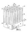
- FIG. 1is a perspective view of an anodic aluminum oxide layer that may be formed by method embodiments of the present invention.
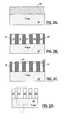
- FIGS. 2A-2Hare cross-sectional views of intermediate structures that illustrate methods of forming vertical surround gate field effect transistors according to embodiments of the present invention.
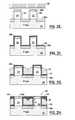
- FIGS. 3A-3Gare cross-sectional views of intermediate structures that illustrate methods of forming vertical surround gate field effect transistors according to additional embodiments of the present invention.
- FIGS. 4A-4Dare cross-sectional views of intermediate structures that illustrate methods of forming opto-electronic devices according to embodiments of the present invention.
- FIGS. 5A-5Fare cross-sectional views of intermediate structures that illustrate methods of forming opto-electronic devices according to additional embodiments of the present invention.
- first conductivity typeand “second conductivity type” refer to opposite conductivity types such as N or P-type, however, each embodiment described and illustrated herein includes its complementary embodiment as well.
- a nanoporous anodic aluminum oxide (AAO) thin film 10may include an array of hexagonal-shaped columnar cells 12 having respective nanopores 14 therein that may also be referred to herein as “nano-channels.” Each of the cells 12 is illustrated as having a diameter “D c ” that may be in a range between about 25 nm and about 400 nm and each of the nanopores 14 may have a diameter “D p ” in a range between about 8 nm and about 50 nm.
- the bottom of the nanopores 14may be separated from an underlying aluminum substrate 20 by an anodic aluminum oxide barrier layer 16 .
- the anodic aluminum oxide barrier layer 16typically has a thickness “t b ” in a range between about 10 nm and about 150 nm.
- the AAO thin film 10may be formed by repeatedly exposing the aluminum substrate 20 to an anodization process that may be integrated within an electrochemical batch process.
- These methods of forming nanoporous AAO thin films 10may include initial steps to mechanically polish an aluminum (Al) substrate 20 .
- the mechanical polishing stepmay include using a diamond paste (e.g., 3 ⁇ m) and a silica ( ⁇ 20 nm) aqueous suspension within a conventional polishing tool.
- the aluminum substrate 20is preferably a high purity (e.g., 99.997% Al) substrate that has been treated under a high pressure press (e.g., ⁇ 1 ⁇ 10 6 psi) to flatten the substrate 20 prior to polishing.
- the aluminum substrate 20may then be thermally annealed in an N 2 ambient at a temperature of about 350° C.
- annealing temperatureof about 400° C. and an annealing time of about 30 minutes may also be used. Annealing times and temperatures that provide similar thermal treatments may also be used.
- the aluminum substrate 20is then exposed to an electrochemical polishing step with a preferred electrolyte at a voltage of about 20 V and a temperature of about 84° C., in some embodiments.
- the preferred electrolytemay include a solution of H 3 PO 4 (95 vol %), H 2 SO 4 (5 vol %) and CrO 3 (20 g/liter).
- the aluminum substrate 20is treated repeatedly to an anodization process to improve the uniformity of the AAO thin film 10 and achieve a desired AAO thin film 10 thickness in a gradual manner. Pre-patterning techniques may also be used to improve the uniformity of the AAO.
- the diameter and length of the nanopores 14can be controlled by adjusting the electrolyte composition and concentration and the anodization voltage and time.
- FIGS. 2A-2Hillustrate methods of forming N-channel surround gate nano-scale MOSFETs that do not require photolithographically controlled patterning steps to define channel length and gate electrode feature size.
- a silicon substrate 30e.g., P-type
- the aluminum layer 20 ′may have a thickness in a range between about 100 nm and about 5000 nm.
- a thin barrier layermay also be formed on the silicon substrate 30 in order to improve adhesion between the aluminum layer 20 ′ and the silicon substrate 30 and act as a conductive layer to facilitate an anodization process.
- This barrier layermay include a conductive titanium layer having a thickness of about 5-20 nm. Other conductive materials besides titanium may also be used.
- the barrier layermay be formed by thermal evaporation or sputtering.
- the aluminum layer 20 ′is then converted into a nanoporous anodic aluminum oxide (AAO) thin film 10 ′ using, in one exemplary embodiment, the methods described above with respect to FIG. 1 . These methods may include a repeated anodization process.
- AAOnanoporous anodic aluminum oxide
- the anodization processmay be stopped before the entire aluminum layer 20 ′ is converted into aluminum oxide (Al 2 O 3 ) and any residual aluminum or insulating material (e.g., SiO 2 ) at the bottoms of the nanopores 14 ′ may be removed using an etching step (e.g., ion etching). This etching step may result in exposure of the underlying silicon substrate 30 at the locations defined by the nanopores 14 ′.
- an etching stepe.g., ion etching
- nano-scale silicon pillars 32are then formed inside the nanopores 14 ′.
- These silicon pillars 32may be formed as monocrystalline silicon pillars using selective epitaxial growth (SEG) techniques and the exposed portions of the underlying silicon substrate 30 as growth “seeds”.
- the growth of the silicon pillars 32may include a low temperature ( ⁇ 800° C.) selective epitaxial growth step using an ultra high vacuum rapid thermal chemical vapor deposition process (UHV-CVD), with or without chlorine.
- UHV-CVDultra high vacuum rapid thermal chemical vapor deposition process
- Such an epitaxial growth stepcan be used to produce high quality, facet free silicon pillars 32 having an average diameter in a range between about 8 nm and about 50 nm.
- the epitaxial growth stepmay include in-situ doping of the silicon pillars 32 to achieve desired electrical properties.
- the duration of the epitaxial growth stepmay be sufficiently long to provide silicon pillars 32 having an average height in a range between about 10 nm and about 100 nm.
- the vertical openings defined by the array of nanopores 14 ′may be transferred to an underlying insulating layer, which can be used as a template for epitaxial growth.
- the silicon pillars 32may be formed by depositing a blanket layer of amorphous silicon (a-Si) on an upper surface of the AAO thin film 10 ′ and into the nanopores 14 ′.
- a-Siamorphous silicon
- the deposited a-Si layer(not shown) may then be planarized using a conventional technique such as chemical-mechanical polishing (CMP).
- CMPchemical-mechanical polishing
- the remaining amorphous silicon pillars within the pores 14 ′are then recyrstallized using, for example, a solid phase recrystallization process.
- the AAO thin film 10 ′is selectively removed to expose an array of free-standing silicon pillars 32 , as illustrated by FIG. 2 D.
- FIG. 2Ewhich represents an enlarged cross-sectional view of a highlighted portion of the structure illustrated by FIG. 2D
- a stepis performed to protect sidewalls of the silicon pillars 32 .
- This stepmay include depositing a blanket layer of an electrically insulating material, such as silicon dioxide or silicon nitride, and then anisotropically etching back the deposited layer to define sidewall spacers 34 that surround the silicon pillars 32 and expose an upper surface of the silicon substrate 30 and upper surfaces of the silicon pillars 32 .
- N-type source and drain region dopants 36are then implanted into the exposed surfaces, as illustrated.
- the dopantsare thermally activated to define a contiguous mesh-shaped source region 38 a in the silicon substrate 30 and also define a plurality of drain regions 38 b that extend adjacent upper surfaces of the silicon pillars 32 .
- the protective sidewall spacers 34may then be removed to expose sidewalls of the silicon pillars 32 .
- the upper surface of the silicon substrate 30may include a semiconductor layer that is relatively highly doped and need not be exposed to receive source region dopants 36 . In these embodiments, the sidewall spacers 34 need not be defined using an etch-back step.
- a conformal gate oxide layer 40may be formed on the silicon pillars 32 using a thermal oxidation step. Other techniques for depositing a gate oxide layer 40 may also be used.
- a blanket conductive layere.g., polysilicon, metal
- a blanket electrically insulating passivation layer 44may then be deposited and planarized to expose the drain regions 38 b at the upper surfaces of the silicon pillars 32 .
- a vertical surround gate field effect transistor 50having an overall effective channel width that is proportional to a product of a width of each pillar 32 and the number of pillars 32 , can be formed.
- the channel length “L c ” of the transistoris equal to the height of the silicon pillars 32 minus the depth of the drain regions 38 b , as illustrated.
- the methodsinclude forming a substrate comprising a semiconductor layer 50 and a substrate insulating layer 52 on the semiconductor layer 50 .
- the semiconductor layer 50may be formed within a semiconductor wafer and may be of first conductivity type (e.g., P-type). In alternative embodiments, the semiconductor layer may be of second conductivity type (e.g., N-type).
- the substrate insulating layer 52may comprise a silicon dioxide layer having a thickness in a range between about 10 nm and 200 nm or possible thicker. An etching template is formed on the substrate insulating layer 52 .
- the etching templatemay be formed by a sequence of steps including thermally evaporating an aluminum layer 56 on the substrate insulating layer 52 .
- Other metals, including aluminum alloys,may also be used.
- the aluminum layer 56may have a thickness in a range between about 100 nm and about 5 ⁇ m in some embodiments.
- the step of forming the aluminum layer 56may be preceded by an optional step of forming a barrier layer 54 directly on the substrate insulating layer 52 .
- the barrier layer 54may be formed by thermally evaporating a metal layer (e.g., titanium) onto an upper surface of the substrate insulating layer 52 .
- the barrier layer 54may have a thickness in a range between about 5 nm and about 20 nm in some embodiments and may be used as a conductive layer to facilitate anodization of the aluminum layer 56 .
- the barrier metal layer 54may also be used to promote adhesion between the substrate insulating layer 52 and the aluminum layer 56 .
- the aluminum layer 56may be thermally annealed to promote grain growth and electrochemically polished to prepare the surface of the aluminum layer 56 for subsequent processing steps.
- additional steps to form the etching templatemay include repeatedly anodizing the aluminum layer 56 to convert it into an anodic aluminum oxide (AAO) layer 58 having a naturally occurring (and non-photolithographically defined) array of nanopores or nano-channels 58 a therein.
- AAOanodic aluminum oxide
- These nanopores 58 aextend substantially through the entire thickness of the AAO layer 58 (see, e.g., FIG. 1 ).
- Residual aluminum metal at the bottoms of the nanopores 58 amay be removed using a conventional etching step.
- the array of nanopores 58 amay also be transferred to the underlying barrier metal layer 54 using a selective etching step (e.g., reactive ion-beam etching). The duration of this selective etching step should be sufficient to fully penetrate the barrier metal layer 54 and expose an upper surface of the underlying substrate insulating layer 52 .
- the array of nanopores 58 ais advantageously transferred from the etching template to the underlying substrate insulating layer 52 by selectively etching the substrate insulating layer 52 using the etching template ( 58 , 54 ) as an etching mask.
- This selective etching stepresults in the formation of a second array of nanopores 52 a that extend through the substrate insulating layer 52 .
- This selective etching stepmay include ion etching or reactive ion beam etching the substrate insulating layer 52 .
- a cleaning stepmay also be performed using a high vacuum cleaning technique or by exposing the substrate insulating layer 52 to a HF cleaning solution.
- the etching template ( 58 , 54 )is then removed to expose the substrate insulating layer 52 .
- an array of semiconductor nano-pillars 60may be formed in the second array of nanopores 52 a by selectively epitaxially growing monocrystalline pillars 60 into the nanopores 52 a using the underlying semiconductor layer 50 as a seed layer.
- the substrate insulating layer 52may be considerably thinner than the etching template ( 58 , 54 ) in order to reduce the aspect ratio (height/diameter) of the nanopores 52 a that are used to confine the array of semiconductor nano-pillars 60 and improve the efficiency of the selective epitaxial growth step.
- the substrate insulating layer 52is selectively removed to expose the array of semiconductor nano-pillars 60 .
- Conventional stepsmay then be used to define sidewall insulating spacers 62 on sidewalls of the nano-pillars 60 , as illustrated by FIG. 3 E.
- These conventional stepsmay include depositing a blanket passivation layer (not shown) on the nano-pillars 60 and then anisotropically etching back the blanket insulating layer to expose the semiconductor layer 50 and upper surfaces of the nano-pillars 60 .
- Source and drain region dopants 64are then implanted into the nano-pillars 60 and the underlying substrate layer 50 , using the sidewall insulating spacers 62 as an implant mask.
- the implanted dopants 64are then activated and driven-in to define a contiguous mesh-shaped source region 66 a in the semiconductor layer 50 and a plurality of drain regions 66 b in the nano-pillars 60 .
- the sidewall insulating spacers 62are then removed using an etching step.
- a conventional thermal oxidation stepmay then be performed to define a gate oxide insulating layer 68 on the sidewalls of the nano-pillars 60 , as illustrated by FIG. 3 F.
- FIG. 3Grepresents an enlarged cross-sectional view of the highlighted portion of FIG.
- a blanket conductive layer(e.g., polysilicon layer) is deposited onto the semiconductor layer 50 and then etched back to define a mesh-shaped surround gate 70 that extends between the nano-pillars 60 .
- a passivation layer 72may then be deposited to fill recesses between the nano-pillars 60 and cover the surround gate 70 .
- the passivation layer 72is then planarized to expose the drain regions 66 b . This step may be followed by the step of depositing a layer of metallization, which operates as a drain electrode 74 .
- a source electrodemay also be formed in ohmic contact with the contiguous source region 66 a at a remote location (not shown).
- FIGS. 4A-4DThese methods may utilize a variety of III-V (or II-VI) compound semiconductor materials to define opto-electronic light emitting and/or light detecting devices including, but not limited to, semiconductor lasers, light emitting diodes (LEDs) and photodetectors.
- III-Vor II-VI
- an N-type Al x Ga 1 ⁇ x As layer 82may be grown on an underlying compound semiconductor substrate 80 , which is shown as an N+ gallium arsenide (GaAs) substrate.
- GaAsgallium arsenide
- the Al x Ga 1 ⁇ x As layer 82may be grown on the compound semiconductor substrate 80 using a conventional metal-organic chemical vapor deposition (MOCVD) process or a molecular beam epitaxy (MBE) process, for example.
- MOCVDmetal-organic chemical vapor deposition
- MBEmolecular beam epitaxy
- An aluminum metal layer 84is then formed on the Al x Ga 1 ⁇ x As layer 82 .
- the aluminum metal layer 84may be formed using a physical vapor deposition (PVD) process, including evaporation or sputtering. This deposition process may be preceded by the deposition of a protective insulating layer (e.g., SiO 2 ) on the Al x Ga 1 ⁇ x As layer 82 .
- PVDphysical vapor deposition
- the aluminum metal layer 84may also be provided as an epitaxial layer that is formed by continuing the step of epitaxially growing the Al x Ga 1 ⁇ x As layer 82 on the underlying compound semiconductor substrate 80 and gradually reducing the concentration of the gallium (Ga) and arsenic (As) source elements. In the event a PVD process is used, the deposited aluminum metal layer 84 can be thermally annealed to promote grain size growth, as described above.
- the aluminum metal layer 84is then subjected to a repeated anodization process to convert the aluminum metal layer 84 into an anodized aluminum oxide (AAO) layer 86 having a closely-packed highly regular array of nanopores 88 therein.
- AAOanodized aluminum oxide
- These nanoporesmay have an average diameter in a range between about 10 nm and about 100 nm.
- the diameter and density of these nanopores 88may be controlled by adjusting the electrolyte composition and concentration and the anodization voltage and time.
- Various electrolytes, such as oxalic acid, sulfuric acid and phosphoric acidcan be used to obtain AAO layers with desired dimensions.
- a vertical stack of InGaAs/GaAs quantum dotscan be selectively grown inside the nanopores 88 of the AAO layer 86 .
- These quantum dotsare illustrated as a vertical stack of alternating InGaAs dots 90 a and GaAs dots 90 b .
- a selective growth techniquethat provides a high degree of selectivity to Al x Ga 1 ⁇ x As over Al 2 O 3 may be used to efficiently form the vertical stack of quantum dots.
- these quantum dots 90 a / 90 bare grown to completely fill the nanopores 88 in the AAO layer 86 , as illustrated.
- an Al x Ga 1 ⁇ x As layer 92(shown as P-type) can be deposited on the AAO layer 86 , as illustrated by FIG. 4 D. Conventional techniques may then be used to deposit a GaAs cladding layer 94 (shown as P+) on the Al x Ga 1 ⁇ x As layer 92 .
- An alternative method of forming a similar device to the optoelectronic device of FIG. 4Dmay utilize an electrically insulating layer (e.g., SiO 2 ) as a porous growth template having a carefully controlled thickness that matches a height of a desired vertical stack of quantum dots 90 a / 90 b .
- This methodincludes growing an N-type Al x Ga 1 ⁇ x As layer 82 on an underlying compound semiconductor substrate 80 , as illustrated by FIG. 5 A.
- the compound semiconductor substrate 80is shown as an N+ gallium arsenide (GaAs) substrate.
- GaAsgallium arsenide
- a silicon dioxide layer 96 or other acceptable insulating material layeris then deposited on the Al x Ga 1 ⁇ x As 82 , as illustrated by FIG. 5 B.
- the step of depositing the silicon dioxide layer 96may be followed by a step to form a barrier metal layer (e.g., titanium barrier layer) on the silicon dioxide layer 96 .
- a barrier metal layere.g., titanium barrier layer
- An aluminum metal layer 84is then formed on the silicon dioxide layer 96 (or barrier metal layer).
- the aluminum metal layer 84may be formed using a physical vapor deposition process (PVD), including evaporation or sputtering.
- PVDphysical vapor deposition process
- the aluminum metal layer 84is subjected to a repeated anodization process to convert the aluminum metal layer 84 into an anodized aluminum oxide (AAO) layer 86 having a closely-packed highly regular array of nanopores 88 therein.
- AAOanodized aluminum oxide
- the silicon dioxide layer 96may be selectively etched using the anodized aluminum oxide layer 86 as an etching mask. This selective etching step results in a transfer of the array of nanopores 88 in the AAO layer 86 to the underlying silicon dioxide layer 96 .
- a vertical stack of InGaAs/GaAs quantum dotscan be selectively grown inside the transferred array of nanopores 98 .
- These dotsare illustrated as a vertical stack of alternating InGaAs dots 90 a and GaAs dots 90 b .
- a selective growth techniquethat provides a high degree of selectivity to Al x Ga 1 ⁇ x As over SiO 2 may be used to efficiently form the vertical stack of quantum dots.
- these quantum dots 90 a / 90 bare grown to completely fill the transferred array of nanopores 98 in the silicon dioxide layer 96 .
- an Al x Ga 1 ⁇ x As layer 92(shown as P-type) can be deposited on the silicon dioxide layer 96 , as illustrated in FIG. 5 F.
- Conventional techniquesmay then be used to deposit a GaAs cladding layer 94 (shown as P+) on the Al x Ga 1 ⁇ x As layer 92 in the event these layers are necessary to complete the opto-electronic device.
- ohmic contactscan be made to the N+GaAs substrate 80 and the P+ GaAs cladding layer 94 and a cavity can be formed by conventional cutting or cleaving.
- the lateral size distribution of the vertical quantum dot stackcan also be controlled by the channel diameter of the AAO thin film 86 .
- the height distribution of the quantum dotsmay be controlled at an atomic level and because the heights may be substantially smaller than the diameter of the dots (i.e., pallet shaped), any performance degradation caused by diameter variation can be made less significant.
- the lateral coupling of the quantum dotscan be treated as negligible because of the wide bandgap of the insulating material between the channels (Al 2 O 3 or SiO 2 ).
Landscapes
- Engineering & Computer Science (AREA)
- Physics & Mathematics (AREA)
- Condensed Matter Physics & Semiconductors (AREA)
- General Physics & Mathematics (AREA)
- Manufacturing & Machinery (AREA)
- Computer Hardware Design (AREA)
- Microelectronics & Electronic Packaging (AREA)
- Power Engineering (AREA)
- Chemical & Material Sciences (AREA)
- Materials Engineering (AREA)
- Nanotechnology (AREA)
- Mathematical Physics (AREA)
- Theoretical Computer Science (AREA)
- Crystallography & Structural Chemistry (AREA)
- Thin Film Transistor (AREA)
- Insulated Gate Type Field-Effect Transistor (AREA)
Abstract
Description
This application claims priority to Provisional Application Ser. Nos. 60/300,804, filed Jun. 25, 2001 and 60/301,018, filed Jun. 26, 2001, the disclosures of which are hereby incorporated herein by reference.
This invention was made with Government support under Contract No. N66001-01-1-8977, awarded by SPAWAR/DARPA. The Government may have certain rights in this invention.
The present invention relates to methods of forming integrated circuit devices and device formed thereby and, more particularly, to methods of forming integrated circuit devices having nano-scale features therein and integrated circuit devices formed thereby.
As semiconductor devices scale down to nano-scale dimensions (i.e., ≦100 nm features), the performance improvements predicted by Moore's Law typically diminish. Some fundamental physical properties, such as direct quantum tunneling through gate dielectrics, poly depletion in gate electrodes and source-drain leakage due to short channel effects, may become limiting factors in performance and may inhibit further scaling of conventional devices.
One method to suppress short channel effects in field effect transistors is to make the semiconductor channel of the transistor sufficiently thin that it becomes fully depleted during operation. One such device is a planar thin-body semiconductor-on-insulator (SOI) transistor, where the source-drain leakage current can be controlled by a high quality back oxide. However, the thin-body SOI transistor may suffer from poor drain-induced barrier lowering and significant short channel threshold voltage reduction due to reach-through of the drain field through a bulk oxide region. The dual-gate MOSFET with both a front gate and a back gate can provide an effective solution to the problems encountered by thin-body SOI transistors. An extension of the dual-gate transistor is the surround gate transistor, which includes a gate that wraps around (i.e., surrounds) the channel.
Several double/surround gate devices that have been proposed can be classified as either horizontal devices or vertical devices. In horizontal devices, the gate length can be defined using photolithography techniques. However, conventional photolithography techniques may not efficiently scale to nano-scale dimensions. In vertical devices, conventional photolithography techniques may not be required to achieve nano-scale dimensions. For example, in vertical field effect transistors, the gate length and other features may be defined by film thickness instead of a photolithographically defined line width. Conventional vertical devices, such as surround gate transistors, are disclosed in an article by E. Leobandung et al. entitled “Wire-Channel and Wrap-Around-Gate Metal-Oxide-Semiconductor Field-Effect Transistors with a Significant Reduction of Short Channel Effects,” J. Vac. Sci. Technol., B 15(6), pp. 2791-2794, November/December (1997). Vertical devices are also disclosed in an article by C. Auth et al., entitled “Scaling Theory for Cylindrical, Fully-Depleted, Surrounding-Gate MOSFET's,” IEEE Elec. Dev. Lett., Vol. 18, No. 2, pp. 74-76, February (1997).
Additional devices that utilize nano-scale metal or semiconductor materials may be formed using nanowires. When wires fabricated from metal or semiconductor materials are provided in the nanometer size range, some of the electronic and optical properties of the metal or semiconductor materials at nano-scale dimensions may be different from the same properties of the same materials at a larger scale. Semiconductor structures in the nanometer size range that exhibit the characteristics of quantum confinement are typically referred to as zero-dimension (OD) quantum dots or more simply as quantum dots when the confinement is in three dimensions. Quantum dots may be provided by semiconductor materials having one or more dimensions on the scale of about ten nanometers or less. When quantum confinement is in two dimensions, the structures are typically referred to as one-dimensional quantum wires or more simply as quantum wires. A quantum wire is a wire having a diameter sufficiently small to cause confinement of an electron gas in directions that extend normal to the wire.
A prior art technique for fabricating quantum wires may utilize a micro-photolithographic process followed by a metalorganic chemical vapor deposition (MOCVD) process. This technique may be used to generate a single quantum wire or a row of gallium arsenide (GaAs) quantum wires embedded within a bulk aluminum arsenide (AlAs) substrate. However, such techniques may not be compatible with processes to form two or three dimensional arrays of nanowires in which the spacing between nanowires is relatively small and uniform.
Additional techniques for forming two-dimensional arrays of nano-channels include filling naturally occurring arrays of nano-channels or nanopores in a substrate with a material of interest. In this manner, the substrate is used as a template. Exemplary substrates include anodic aluminum oxide and mesoporous materials, which may be provided with arrays of pores therein. In particular, U.S. Pat. No. 6,359,288 to Ying et al. discloses techniques for forming arrays of nanowires in anodic aluminum oxide substrates. One of these techniques includes systematically changing the channel diameter and channel packing density of an anodic aluminum oxide layer by anodizing an aluminum layer with an electrolyte to provide an anodic aluminum oxide layer having nanopores therein. The mean pore diameter is disclosed as varying by no more than 100% along the length of the pore. The '288 patent also discloses filling the pores with single crystal material so that the resulting nanowires constitute single crystal quantum wires. These quantum wires may have an average wire diameter in a range of about 1 nm to about 20 nm. U.S. Pat. No. 6,231,744 to Ying et al. also discloses a method of forming a nanowire array by anodizing an aluminum substrate using an acidic electrolyte solution to provide a porous aluminum oxide film (i.e., anodic aluminum oxide (AAO) film) on a surface of an aluminum substrate. The porous AAO film is then exposed to an acid etchant solution for a period of time sufficient to enlarge the cell size of the pores.
Techniques for forming porous films and nano-scale electronic devices are disclosed in European Patent Specification No. EP 0 178 831 B1 and in U.S. Pat. No. 6,034,468 to Wilshaw. In particular, the '468 patent to Wilshaw discloses a field emitter device having a dielectric AAO layer therein with nanopores. The front ends of the wires constitute individual field emitting cathodes. A gate electrode is also provided on a front surface of the AAO layer. U.S. Pat. No. 5,581,091 to Moskovits et al. also discloses single-electron devices that are useful as diodes and transistors. These devices are prepared by anodizing a metal substrate in an acid bath to convert the metal substrate into an oxide film.
Embodiments of the present invention include nano-scale electronic devices and methods of forming nano-scale electronic devices using techniques that advantageously have a reduced number of photolithographically defined processing steps. Some of these electronic devices constitute field effect transistors having surround gates that provide fully depleted operation. Other embodiments include opto-electronic devices that contain compound semiconductor materials.
Methods according to embodiments of the present invention include forming a vertical nano-scale electronic device by forming a substrate having a semiconductor layer therein and a substrate insulating layer on the semiconductor layer. The substrate insulating layer may contact an upper surface of the semiconductor layer. A step is then performed to form an etching template having a first array of non-photolithographically defined nano-channels extending therethrough, on the substrate insulating layer. This etching template may comprise an anodized metal oxide, such as an anodized aluminum oxide (AAO) thin film. The substrate insulating layer is then selectively etched to define a second array of nano-channels therein. This selective etching step preferably uses the etching template as an etching mask to transfer the first array of nano-channels to the underlying substrate insulating layer, which may be thinner than the etching template. An array of semiconductor nano-pillars is then formed in the second array of nano-channels. The semiconductor nano-pillars in the array may have an average diameter in a range between about 8 nm and about 50 nm. The semiconductor nano-pillars are also preferably homoepitaxial or heteroepitaxial with the semiconductor layer.
The step of forming an etching template may include forming a metal film (e.g., aluminum film) on the substrate insulating layer and then repeatedly anodizing the metal film to convert it into an anodic metal oxide layer having nano-channels therein. The selective etching step may also include ion etching or reactive ion beam etching the insulating layer for a sufficient duration to penetrate the substrate insulating layer and expose the semiconductor layer. The semiconductor layer may also constitute a monocrystalline semiconductor layer and the step of forming an array of semiconductor nano-pillars may include epitaxially growing monocrystalline semiconductor nano-pillars using the monocrystalline semiconductor layer as a seed layer.
These methods may also include the steps of removing the substrate insulating layer to expose the semiconductor nano-pillars and then implanting dopants of first conductivity type into upper surfaces of the semiconductor nano-pillars to define respective drain regions therein. Gate insulating layers are then formed on sidewalls of the semiconductor nano-pillars. A global surround gate electrode may then be formed that extends on the gate insulating layers and in recesses between the semiconductor nano-pillars. A drain electrode may be formed that contacts the drain regions in the semiconductor nano-pillars.
The step of forming a drain electrode may be preceded by the step of depositing an electrically insulating passivation layer on the surround gate electrode and etching-back the passivation layer to expose the upper surfaces of the semiconducting nano-pillars. The step of implanting dopants may also be preceded by the steps of forming a sacrificial protective layer on upper surfaces and sidewalls of the semiconductor nano-pillars and then etching-back the sacrificial protective layer to expose the upper surfaces of the semiconducting nano-pillars. The sacrificial protective layer may then be removed entirely before the gate insulating layer is formed on sidewalls of the semiconducting nano-pillars.
Additional methods of forming vertical nano-scale electronic devices may include forming a substrate comprising a semiconductor layer, a substrate insulating layer on the semiconductor layer and a barrier metal layer on the substrate insulating layer. An etching template is then formed on the substrate insulating layer. The etching template has a first array of non-photolithographically defined nano-channels or nanopores extending therethrough. The etching template may be formed by depositing a metal film (e.g., aluminum film) on the barrier metal layer and then anodizing the metal film into an anodic metal oxide layer having an array of nanopores therein. The barrier metal layer is then selectively etched so that the nanopores extend through the barrier metal layer and expose the substrate insulating layer. The anodic metal oxide layer and the barrier metal layer collectively form the etching template. The substrate insulating layer is then selectively etched for a sufficient duration to define a second array of nano-channels therein and expose the semiconductor layer. The substrate insulating layer may comprise silicon dioxide or silicon nitride, for example. Other electrically insulating materials may also be used. This etching step is performed in order to transfer the pattern of the first array of nano-channels in the etching template to the underlying substrate insulating layer. Selective growth techniques may then be used to grow an array of semiconductor nano-pillars that extend upward from the semiconductor layer and into the second array of nano-channels.
Methods of forming nano-scale opto-electronic devices are also provided by embodiments of the present invention. These methods may include forming a substrate comprising a first compound semiconductor layer of first conductivity type that is a composite of first and second III-V semiconductor materials (e.g., GaAs and AlGaAs). An electrically insulating layer (e.g., SiO2) is then formed on the first semiconductor layer. A step is performed to form a metal thin film on the electrically insulating layer. The metal thin film is converted into an anodized metal oxide layer having an array of nanopores therein. This step to convert the metal thin film into an anodized metal oxide layer is preferably performed without using a photolithographically defined mask to guide the conversion process. The array of nanopores within the anodized metal oxide layer is then transferred to the electrically insulating layer. An array of vertical quantum-dot superlattices is epitaxially grown upward from the underlying first semiconductor layer, using the array of nanopores to guide the epitaxial growth step. A second compound semiconductor layer of second conductivity type may be formed on the array of vertical quantum-dot superlattices. This second compound semiconductor layer may comprise a composite of the first and second III-V semiconductor materials, for example.
Additional embodiments of the present invention include preferred optoelectronic devices that contain arrays of vertical quantum-dot superlattices therein. An optoelectronic device may include a substrate having a first III-V semiconductor layer therein. An electrically insulating layer is also provided that extends on the first III-V semiconductor layer. This electrically insulating layer includes an array of non-photolithographically defined nanopores therein. An array of vertical quantum-dot superlattices are provided in the array of nanopores. These vertical quantum-dot superlattices are electrically coupled to the first III-V semiconductor layer. The optoelectronic device may also include a second III-V semiconductor layer that extends on the array of vertical quantum-dot superlattices. According to a preferred aspect of this embodiment, the first and second III-V semiconductor layers are homoepitaxial or heteroepitaxial with the vertical quantum-dot superlattices.
FIG. 1 is a perspective view of an anodic aluminum oxide layer that may be formed by method embodiments of the present invention.
FIGS. 2A-2H are cross-sectional views of intermediate structures that illustrate methods of forming vertical surround gate field effect transistors according to embodiments of the present invention.
FIGS. 3A-3G are cross-sectional views of intermediate structures that illustrate methods of forming vertical surround gate field effect transistors according to additional embodiments of the present invention.
FIGS. 4A-4D are cross-sectional views of intermediate structures that illustrate methods of forming opto-electronic devices according to embodiments of the present invention.
FIGS. 5A-5F are cross-sectional views of intermediate structures that illustrate methods of forming opto-electronic devices according to additional embodiments of the present invention.
The present invention will now be described more fully hereinafter with reference to the accompanying drawings, in which preferred embodiments of the invention are shown. This invention may, however, be embodied in different forms and should not be construed as limited to the embodiments set forth herein. Rather, these embodiments are provided so that this disclosure will be thorough and complete, and will fully convey the scope of the invention to those skilled in the art. In the drawings, the thickness of layers and regions are exaggerated for clarity. It will also be understood that when a layer is referred to as being “on” another layer or substrate, it can be directly on the other layer or substrate, or intervening layers may also be present. Moreover, the terms “first conductivity type” and “second conductivity type” refer to opposite conductivity types such as N or P-type, however, each embodiment described and illustrated herein includes its complementary embodiment as well.
Methods of forming self-assembled nanoporous anodic aluminum oxide thin films according to embodiments of the present invention will now be described. As illustrated best by FIG. 1, a nanoporous anodic aluminum oxide (AAO)thin film 10 may include an array of hexagonal-shapedcolumnar cells 12 havingrespective nanopores 14 therein that may also be referred to herein as “nano-channels.” Each of thecells 12 is illustrated as having a diameter “Dc” that may be in a range between about 25 nm and about 400 nm and each of thenanopores 14 may have a diameter “Dp” in a range between about 8 nm and about 50 nm. The bottom of thenanopores 14 may be separated from anunderlying aluminum substrate 20 by an anodic aluminumoxide barrier layer 16. The anodic aluminumoxide barrier layer 16 typically has a thickness “tb” in a range between about 10 nm and about 150 nm. As described more fully hereinbelow, the AAOthin film 10 may be formed by repeatedly exposing thealuminum substrate 20 to an anodization process that may be integrated within an electrochemical batch process.
These methods of forming nanoporous AAOthin films 10 according to embodiments of the present invention may include initial steps to mechanically polish an aluminum (Al)substrate 20. The mechanical polishing step may include using a diamond paste (e.g., 3 μm) and a silica (˜20 nm) aqueous suspension within a conventional polishing tool. Thealuminum substrate 20 is preferably a high purity (e.g., 99.997% Al) substrate that has been treated under a high pressure press (e.g., ˜1×10⁶psi) to flatten thesubstrate 20 prior to polishing. Thealuminum substrate 20 may then be thermally annealed in an N2ambient at a temperature of about 350° C. for about 1 hour to promote grain growth and achieve a relatively large average grain size (e.g., 3-5 μm). An annealing temperature of about 400° C. and an annealing time of about 30 minutes may also be used. Annealing times and temperatures that provide similar thermal treatments may also be used.
Thealuminum substrate 20 is then exposed to an electrochemical polishing step with a preferred electrolyte at a voltage of about 20 V and a temperature of about 84° C., in some embodiments. The preferred electrolyte may include a solution of H3PO4(95 vol %), H2SO4(5 vol %) and CrO3(20 g/liter). Thealuminum substrate 20 is treated repeatedly to an anodization process to improve the uniformity of the AAOthin film 10 and achieve a desired AAOthin film 10 thickness in a gradual manner. Pre-patterning techniques may also be used to improve the uniformity of the AAO. The diameter and length of thenanopores 14 can be controlled by adjusting the electrolyte composition and concentration and the anodization voltage and time.
Methods of forming nano-scale field effect transistors according to embodiments of the present invention may utilize the AAOthin films 10 of FIG.1. In particular, FIGS. 2A-2H illustrate methods of forming N-channel surround gate nano-scale MOSFETs that do not require photolithographically controlled patterning steps to define channel length and gate electrode feature size. In FIG. 2A, a silicon substrate30 (e.g., P-type) is provided with analuminum layer 20′ thereon. Thealuminum layer 20′ may have a thickness in a range between about 100 nm and about 5000 nm. A thin barrier layer (not shown) may also be formed on thesilicon substrate 30 in order to improve adhesion between thealuminum layer 20′ and thesilicon substrate 30 and act as a conductive layer to facilitate an anodization process. This barrier layer may include a conductive titanium layer having a thickness of about 5-20 nm. Other conductive materials besides titanium may also be used. The barrier layer may be formed by thermal evaporation or sputtering. As illustrated by FIG. 2B, thealuminum layer 20′ is then converted into a nanoporous anodic aluminum oxide (AAO)thin film 10′ using, in one exemplary embodiment, the methods described above with respect to FIG.1. These methods may include a repeated anodization process. The anodization process may be stopped before theentire aluminum layer 20′ is converted into aluminum oxide (Al2O3) and any residual aluminum or insulating material (e.g., SiO2) at the bottoms of thenanopores 14′ may be removed using an etching step (e.g., ion etching). This etching step may result in exposure of theunderlying silicon substrate 30 at the locations defined by thenanopores 14′.
Referring now to FIG. 2C, nano-scale silicon pillars 32 are then formed inside thenanopores 14′. Thesesilicon pillars 32 may be formed as monocrystalline silicon pillars using selective epitaxial growth (SEG) techniques and the exposed portions of theunderlying silicon substrate 30 as growth “seeds”. The growth of thesilicon pillars 32 may include a low temperature (˜800° C.) selective epitaxial growth step using an ultra high vacuum rapid thermal chemical vapor deposition process (UHV-CVD), with or without chlorine. Such an epitaxial growth step can be used to produce high quality, facetfree silicon pillars 32 having an average diameter in a range between about 8 nm and about 50 nm. The epitaxial growth step may include in-situ doping of thesilicon pillars 32 to achieve desired electrical properties. The duration of the epitaxial growth step may be sufficiently long to providesilicon pillars 32 having an average height in a range between about 10 nm and about 100 nm. As explained more fully hereinbelow, the vertical openings defined by the array ofnanopores 14′ may be transferred to an underlying insulating layer, which can be used as a template for epitaxial growth. In alternative embodiments, thesilicon pillars 32 may be formed by depositing a blanket layer of amorphous silicon (a-Si) on an upper surface of the AAOthin film 10′ and into thenanopores 14′. The deposited a-Si layer (not shown) may then be planarized using a conventional technique such as chemical-mechanical polishing (CMP). The remaining amorphous silicon pillars within thepores 14′ are then recyrstallized using, for example, a solid phase recrystallization process.
The AAOthin film 10′ is selectively removed to expose an array of free-standingsilicon pillars 32, as illustrated by FIG.2D. Referring now to FIG. 2E, which represents an enlarged cross-sectional view of a highlighted portion of the structure illustrated by FIG. 2D, a step is performed to protect sidewalls of thesilicon pillars 32. This step may include depositing a blanket layer of an electrically insulating material, such as silicon dioxide or silicon nitride, and then anisotropically etching back the deposited layer to definesidewall spacers 34 that surround thesilicon pillars 32 and expose an upper surface of thesilicon substrate 30 and upper surfaces of thesilicon pillars 32. N-type source and drainregion dopants 36 are then implanted into the exposed surfaces, as illustrated. The dopants are thermally activated to define a contiguous mesh-shapedsource region 38ain thesilicon substrate 30 and also define a plurality ofdrain regions 38bthat extend adjacent upper surfaces of thesilicon pillars 32. Theprotective sidewall spacers 34 may then be removed to expose sidewalls of thesilicon pillars 32. In alternative embodiments, the upper surface of thesilicon substrate 30 may include a semiconductor layer that is relatively highly doped and need not be exposed to receive source region dopants36. In these embodiments, thesidewall spacers 34 need not be defined using an etch-back step.
Referring now to FIG. 2F, a conformalgate oxide layer 40 may be formed on thesilicon pillars 32 using a thermal oxidation step. Other techniques for depositing agate oxide layer 40 may also be used. A blanket conductive layer (e.g., polysilicon, metal) may be deposited on thegate oxide layer 40 and etched back to define apolysilicon gate electrode 42 that surrounds the array ofsilicon pillars 32, as illustrated by FIG.2G. Because the source and drainregions gate electrode 42, the methods described herein may be compatible with high-K dielectrics and metal gate electrodes materials may be used. As illustrated by FIG. 2H, a blanket electrically insulatingpassivation layer 44 may then be deposited and planarized to expose thedrain regions 38bat the upper surfaces of thesilicon pillars 32. In this manner, a vertical surround gatefield effect transistor 50 having an overall effective channel width that is proportional to a product of a width of eachpillar 32 and the number ofpillars 32, can be formed. The channel length “Lc” of the transistor is equal to the height of thesilicon pillars 32 minus the depth of thedrain regions 38b, as illustrated.
Additional methods of forming vertical surround gate field effect transistors will now be more fully described with respect to FIGS. 3A-3G. As illustrated by FIG. 3A, the methods include forming a substrate comprising asemiconductor layer 50 and asubstrate insulating layer 52 on thesemiconductor layer 50. Thesemiconductor layer 50 may be formed within a semiconductor wafer and may be of first conductivity type (e.g., P-type). In alternative embodiments, the semiconductor layer may be of second conductivity type (e.g., N-type). Thesubstrate insulating layer 52 may comprise a silicon dioxide layer having a thickness in a range between about 10 nm and 200 nm or possible thicker. An etching template is formed on thesubstrate insulating layer 52. The etching template may be formed by a sequence of steps including thermally evaporating analuminum layer 56 on thesubstrate insulating layer 52. Other metals, including aluminum alloys, may also be used. Thealuminum layer 56 may have a thickness in a range between about 100 nm and about 5 μm in some embodiments. The step of forming thealuminum layer 56 may be preceded by an optional step of forming abarrier layer 54 directly on thesubstrate insulating layer 52. Thebarrier layer 54 may be formed by thermally evaporating a metal layer (e.g., titanium) onto an upper surface of thesubstrate insulating layer 52. Thebarrier layer 54 may have a thickness in a range between about 5 nm and about 20 nm in some embodiments and may be used as a conductive layer to facilitate anodization of thealuminum layer 56. Thebarrier metal layer 54 may also be used to promote adhesion between thesubstrate insulating layer 52 and thealuminum layer 56. As described above with respect to FIGS. 2A-2H, thealuminum layer 56 may be thermally annealed to promote grain growth and electrochemically polished to prepare the surface of thealuminum layer 56 for subsequent processing steps.
As illustrated by FIG. 3B, additional steps to form the etching template may include repeatedly anodizing thealuminum layer 56 to convert it into an anodic aluminum oxide (AAO)layer 58 having a naturally occurring (and non-photolithographically defined) array of nanopores or nano-channels 58atherein. Thesenanopores 58aextend substantially through the entire thickness of the AAO layer58 (see, e.g., FIG.1). Residual aluminum metal at the bottoms of thenanopores 58amay be removed using a conventional etching step. The array ofnanopores 58amay also be transferred to the underlyingbarrier metal layer 54 using a selective etching step (e.g., reactive ion-beam etching). The duration of this selective etching step should be sufficient to fully penetrate thebarrier metal layer 54 and expose an upper surface of the underlyingsubstrate insulating layer 52.
Referring now to FIG. 3C, the array ofnanopores 58ais advantageously transferred from the etching template to the underlyingsubstrate insulating layer 52 by selectively etching thesubstrate insulating layer 52 using the etching template (58,54) as an etching mask. This selective etching step results in the formation of a second array ofnanopores 52athat extend through thesubstrate insulating layer 52. This selective etching step may include ion etching or reactive ion beam etching thesubstrate insulating layer 52. A cleaning step may also be performed using a high vacuum cleaning technique or by exposing thesubstrate insulating layer 52 to a HF cleaning solution. The etching template (58,54) is then removed to expose thesubstrate insulating layer 52.
Referring now to FIG. 3D, an array of semiconductor nano-pillars 60 may be formed in the second array ofnanopores 52aby selectively epitaxially growingmonocrystalline pillars 60 into thenanopores 52ausing theunderlying semiconductor layer 50 as a seed layer. According to a preferred aspect of these embodiments, thesubstrate insulating layer 52 may be considerably thinner than the etching template (58,54) in order to reduce the aspect ratio (height/diameter) of thenanopores 52athat are used to confine the array of semiconductor nano-pillars 60 and improve the efficiency of the selective epitaxial growth step. After the selective growth step, thesubstrate insulating layer 52 is selectively removed to expose the array of semiconductor nano-pillars 60. Conventional steps may then be used to definesidewall insulating spacers 62 on sidewalls of the nano-pillars 60, as illustrated by FIG.3E. These conventional steps may include depositing a blanket passivation layer (not shown) on the nano-pillars 60 and then anisotropically etching back the blanket insulating layer to expose thesemiconductor layer 50 and upper surfaces of the nano-pillars 60. Source and drainregion dopants 64 are then implanted into the nano-pillars 60 and theunderlying substrate layer 50, using thesidewall insulating spacers 62 as an implant mask.
The implanteddopants 64 are then activated and driven-in to define a contiguous mesh-shapedsource region 66ain thesemiconductor layer 50 and a plurality ofdrain regions 66bin the nano-pillars 60. Thesidewall insulating spacers 62 are then removed using an etching step. A conventional thermal oxidation step may then be performed to define a gateoxide insulating layer 68 on the sidewalls of the nano-pillars 60, as illustrated by FIG.3F. Referring now to FIG. 3G, which represents an enlarged cross-sectional view of the highlighted portion of FIG. 3F, a blanket conductive layer (e.g., polysilicon layer) is deposited onto thesemiconductor layer 50 and then etched back to define a mesh-shapedsurround gate 70 that extends between the nano-pillars 60. Apassivation layer 72 may then be deposited to fill recesses between the nano-pillars 60 and cover thesurround gate 70. Thepassivation layer 72 is then planarized to expose thedrain regions 66b. This step may be followed by the step of depositing a layer of metallization, which operates as adrain electrode 74. A source electrode may also be formed in ohmic contact with thecontiguous source region 66aat a remote location (not shown).
Methods of forming opto-electronic devices according to embodiments of the present invention will now be described with reference to FIGS. 4A-4D. These methods may utilize a variety of III-V (or II-VI) compound semiconductor materials to define opto-electronic light emitting and/or light detecting devices including, but not limited to, semiconductor lasers, light emitting diodes (LEDs) and photodetectors. As illustrated by FIG. 4A, an N-type AlxGa1−xAslayer 82 may be grown on an underlyingcompound semiconductor substrate 80, which is shown as an N+ gallium arsenide (GaAs) substrate. The AlxGa1−xAslayer 82 may be grown on thecompound semiconductor substrate 80 using a conventional metal-organic chemical vapor deposition (MOCVD) process or a molecular beam epitaxy (MBE) process, for example. Analuminum metal layer 84 is then formed on the AlxGa1−xAslayer 82. Thealuminum metal layer 84 may be formed using a physical vapor deposition (PVD) process, including evaporation or sputtering. This deposition process may be preceded by the deposition of a protective insulating layer (e.g., SiO2) on the AlxGa1−xAslayer 82. Thealuminum metal layer 84 may also be provided as an epitaxial layer that is formed by continuing the step of epitaxially growing the AlxGa1−xAslayer 82 on the underlyingcompound semiconductor substrate 80 and gradually reducing the concentration of the gallium (Ga) and arsenic (As) source elements. In the event a PVD process is used, the depositedaluminum metal layer 84 can be thermally annealed to promote grain size growth, as described above.
Referring now to FIG. 4B, thealuminum metal layer 84 is then subjected to a repeated anodization process to convert thealuminum metal layer 84 into an anodized aluminum oxide (AAO)layer 86 having a closely-packed highly regular array ofnanopores 88 therein. These nanopores may have an average diameter in a range between about 10 nm and about 100 nm. The diameter and density of thesenanopores 88 may be controlled by adjusting the electrolyte composition and concentration and the anodization voltage and time. Various electrolytes, such as oxalic acid, sulfuric acid and phosphoric acid can be used to obtain AAO layers with desired dimensions.
Referring now to FIG. 4C, a vertical stack of InGaAs/GaAs quantum dots can be selectively grown inside thenanopores 88 of theAAO layer 86. These quantum dots are illustrated as a vertical stack of alternatingInGaAs dots 90aandGaAs dots 90b. A selective growth technique that provides a high degree of selectivity to AlxGa1−xAs over Al2O3may be used to efficiently form the vertical stack of quantum dots. In some embodiments, thesequantum dots 90a/90bare grown to completely fill thenanopores 88 in theAAO layer 86, as illustrated. Following the steps to grow the quantum dots within thenanopores 88, an AlxGa1−xAs layer92 (shown as P-type) can be deposited on theAAO layer 86, as illustrated by FIG.4D. Conventional techniques may then be used to deposit a GaAs cladding layer94 (shown as P+) on the AlxGa1−xAslayer 92.
An alternative method of forming a similar device to the optoelectronic device of FIG. 4D may utilize an electrically insulating layer (e.g., SiO2) as a porous growth template having a carefully controlled thickness that matches a height of a desired vertical stack ofquantum dots 90a/90b. This method includes growing an N-type AlxGa1−xAslayer 82 on an underlyingcompound semiconductor substrate 80, as illustrated by FIG.5A. Thecompound semiconductor substrate 80 is shown as an N+ gallium arsenide (GaAs) substrate. Asilicon dioxide layer 96 or other acceptable insulating material layer is then deposited on the AlxGa1−xAs82, as illustrated by FIG.5B. The step of depositing thesilicon dioxide layer 96 may be followed by a step to form a barrier metal layer (e.g., titanium barrier layer) on thesilicon dioxide layer 96. Analuminum metal layer 84 is then formed on the silicon dioxide layer96 (or barrier metal layer). Thealuminum metal layer 84 may be formed using a physical vapor deposition process (PVD), including evaporation or sputtering.
Referring now to FIG. 5C, thealuminum metal layer 84 is subjected to a repeated anodization process to convert thealuminum metal layer 84 into an anodized aluminum oxide (AAO)layer 86 having a closely-packed highly regular array ofnanopores 88 therein. Referring now to FIG. 5D, thesilicon dioxide layer 96 may be selectively etched using the anodizedaluminum oxide layer 86 as an etching mask. This selective etching step results in a transfer of the array ofnanopores 88 in theAAO layer 86 to the underlyingsilicon dioxide layer 96. As illustrated by FIGS. 5D-5E, a vertical stack of InGaAs/GaAs quantum dots can be selectively grown inside the transferred array ofnanopores 98. These dots are illustrated as a vertical stack of alternatingInGaAs dots 90aandGaAs dots 90b. A selective growth technique that provides a high degree of selectivity to AlxGa1−xAs over SiO2may be used to efficiently form the vertical stack of quantum dots. In some embodiments, thesequantum dots 90a/90bare grown to completely fill the transferred array ofnanopores 98 in thesilicon dioxide layer 96. Following the steps to grow the quantum dots, an AlxGa1−xAs layer92 (shown as P-type) can be deposited on thesilicon dioxide layer 96, as illustrated in FIG.5F. Conventional techniques may then be used to deposit a GaAs cladding layer94 (shown as P+) on the AlxGa1−xAslayer 92 in the event these layers are necessary to complete the opto-electronic device.
In some laser structures, ohmic contacts can be made to the N+GaAs substrate 80 and the P+GaAs cladding layer 94 and a cavity can be formed by conventional cutting or cleaving. The lateral size distribution of the vertical quantum dot stack can also be controlled by the channel diameter of the AAOthin film 86. Moreover, because the height distribution of the quantum dots may be controlled at an atomic level and because the heights may be substantially smaller than the diameter of the dots (i.e., pallet shaped), any performance degradation caused by diameter variation can be made less significant. The lateral coupling of the quantum dots can be treated as negligible because of the wide bandgap of the insulating material between the channels (Al2O3or SiO2).
In the drawings and specification, there have been disclosed typical preferred embodiments of the invention and, although specific terms are employed, they are used in a generic and descriptive sense only and not for purposes of limitation, the scope of the invention being set forth in the following claims.
Claims (22)
1. A method of forming a vertical nano-scale electronic device, comprising the steps of:
forming a substrate comprising a semiconductor layer and a substrate insulating layer on the semiconductor layer;
forming an etching template having a first array of non-photolithographically defined nano-channels extending therethrough, on the substrate insulating layer;
selectively etching the substrate insulating layer to define a second array of nano-channels therein, using the etching template as an etching mask; and
forming an array of semiconductor nano-pillars that extend in the second array of nano-channels and have an average diameter in a range between about 8 nm and about 50 nm.
2. The method ofclaim 1 , wherein said step of forming an etching template comprises forming a nanoporous anodic aluminum oxide thin film on the substrate insulating layer.
3. The method ofclaim 1 , wherein said step of forming an etching template comprises:
forming a metal film on the substrate insulating layer; and
anodizing the metal film into an anodic metal oxide layer.
4. The method ofclaim 1 , wherein said selectively etching step comprises ion etching or reactive ion etching the substrate insulating layer for a sufficient duration to penetrate the substrate insulating layer.
5. The method ofclaim 1 , wherein said selectively etching step comprises ion etching or reactive ion etching the substrate insulating layer for a sufficient duration to penetrate the substrate insulating layer and expose the semiconductor layer.
6. The method ofclaim 5 , wherein the semiconductor layer is a monocrystalline semiconductor layer; and wherein said step of forming an array of semiconductor nano-pillars comprises epitaxially growing monocrystalline semiconductor nano-pillars in the second array of nano-channels.
7. A method ofclaim 6 , further comprising the steps of:
removing the substrate insulating layer to expose sidewalls of the semiconductor nano-pillars;
implanting dopants of first conductivity type into upper surfaces of the semiconductor nano-pillars to define respective drain regions therein;
forming gate insulating layers on the sidewalls of the semiconductor nano-pillars;
forming a gate electrode that extends on the gate insulating layers and in recesses between the semiconductor nano-pillars; and
forming a drain electrode that electrically contacts the drain regions in the semiconducting nano-pillars.
8. The method ofclaim 7 , wherein said step of forming a drain electrode is preceded by the steps of:
depositing an electrically insulating passivation layer on the gate electrode; and
etching-back the passivation layer to expose the upper surfaces of the semiconducting nano-pillars.
9. The method ofclaim 7 , wherein said implanting step is preceded by the steps of:
forming a sacrificial protective layer on upper surfaces and sidewalls of the semiconductor nano-pillars; and
etching-back the sacrificial protective layer to expose the upper surfaces of the semiconducting nano-pillars.
10. The method ofclaim 9 , wherein said step of forming gate insulating layers is preceded by the step of removing the sacrificial protective layer.
11. The method ofclaim 7 , wherein said implanting step is preceded by the steps of:
forming a sacrificial protective layer on upper surfaces and sidewalls of the semiconductor nano-pillars; and
etching-back the sacrificial protective layer to expose the upper surfaces of the semiconductor nano-pillars and expose portions of the underlying substrate.
12. The method ofclaim 11 , wherein said step of forming gate insulating layers is preceded by the step of removing the sacrificial protective layer.
13. The method ofclaim 12 , wherein said implanting step comprises implanting dopants of first conductivity type into the upper surfaces of the semiconductor nano-pillars and the exposed portions of the substrate to define drain and source regions therein.
14. A method ofclaim 1 , further comprising the steps of:
removing the substrate insulating layer to expose sidewalls of the semiconductor nano-pillars;
implanting dopants of first conductivity type into upper surfaces of the semiconductor nano-pillars to define respective drain regions therein;
forming gate insulating layers on the sidewalls of the semiconductor nano-pillars;
forming a gate electrode that extends on the gate insulating layers and in recesses between the semiconductor nano-pillars; and
forming a drain electrode that electrically contacts the drain regions in the semiconducting nano-pillars.
15. A method of forming a vertical nano-scale electronic device, comprising the steps of:
forming a substrate comprising a semiconductor layer, a substrate insulating layer on the semiconductor layer and a barrier metal layer on the substrate insulating layer;
forming an etching template having a first array of non-photolithographically defined nano-channels extending therethrough, on the substrate insulating layer;
selectively etching the substrate insulating layer for a sufficient duration to define a second array of nano-channels therein, using the etching template as an etching mask; and
forming an array of semiconductor nano-pillars that extend in the second array of nano-channels.
16. The method ofclaim 15 , wherein said step of forming an etching template comprises:
forming a metal film on the barrier metal layer;
anodizing the metal film into an anodic metal oxide layer: and
etching the barrier metal layer using the anodic metal oxide layer as an etching mask.
17. A method of forming a vertical nano-scale electronic device, comprising the steps of:
forming a substrate comprising a semiconductor layer and a non-aluminum barrier metal layer on the semiconductor layer;
forming an anodic aluminum oxide layer having an array of nano-sized pores therein, on the barrier metal layer;
selectively etching portions of the barrier metal layer extending adjacent bottoms of the nano-sized pores, using the anodic aluminum oxide layer as an etching mask; and
forming an array of semiconductor nano-pillars that extend in the nano-sized pores.
18. A method of forming a vertical nano-scale opto-electronic device, comprising the steps of:
forming a substrate comprising a first compound semiconductor layer of first conductivity type that is a composite of first and second III-V semiconductor materials;
forming an electrically insulating layer on the first compound semiconductor layer;
forming a metal thin film on the electrically insulating layer;
converting the metal thin film to an anodized metal oxide layer having an array of nanopores therein;
transferring the array of nanopores in the anodized metal oxide layer into the electrically insulating layer;
epitaxially growing an array of vertical quantum-dot superlattices in the array of nanopores in the electrically insulating layer; and
forming a second compound semiconductor layer of second conductivity type that is a composite of the first and second III-V semiconductor materials, on the array of vertical quantum-dot superlattices.
19. A method of forming a vertical nano-scale field effect transistor, comprising the steps of:
forming an electrically insulating layer having an array of nanopores therein;
forming an array of monocrystalline semiconductor nano-pillars in the array of nanopores;
forming a plurality of drain regions in the semiconductor nano-pillars; and
forming a gate electrode that at least partially surrounds the semiconductor nano-pillars.
20. A method of forming a vertical nano-scale opto-electronic device, comprising the steps of:
forming a substrate comprising a first compound semiconductor layer of first conductivity type that is a composite of first and second III-V semiconductor materials;
forming an anodized metal oxide layer having an array of nanopores therein, on the first compound semiconductor layer;
epitaxially growing an array of vertical quantum-dot superlattices in the array of nanopores, using the first compound semiconductor layer as a seed layer; and
forming a second compound semiconductor layer of second conductivity type that is a composite of the first and second III-V semiconductor materials, on the array of vertical quantum-dot superlattices.
21. The method ofclaim 20 , wherein said step of forming an anodized metal oxide layer comprises epitaxially growing an aluminum metal layer on the first compound semiconductor layer.
22. The method ofclaim 21 , wherein the first compound semiconductor layer comprises AlxGa1−xAs.
Priority Applications (3)
| Application Number | Priority Date | Filing Date | Title |
|---|---|---|---|
| US10/178,941US6709929B2 (en) | 2001-06-25 | 2002-06-24 | Methods of forming nano-scale electronic and optoelectronic devices using non-photolithographically defined nano-channel templates |
| US10/760,966US6914256B2 (en) | 2001-06-25 | 2004-01-20 | Optoelectronic devices having arrays of quantum-dot compound semiconductor superlattices therein |
| US11/065,085US7265375B2 (en) | 2001-06-25 | 2005-02-24 | Optoelectonic devices having arrays of quantum-dot compound semiconductor superlattices therein |
Applications Claiming Priority (3)
| Application Number | Priority Date | Filing Date | Title |
|---|---|---|---|
| US30080401P | 2001-06-25 | 2001-06-25 | |
| US30101801P | 2001-06-26 | 2001-06-26 | |
| US10/178,941US6709929B2 (en) | 2001-06-25 | 2002-06-24 | Methods of forming nano-scale electronic and optoelectronic devices using non-photolithographically defined nano-channel templates |
Related Child Applications (1)
| Application Number | Title | Priority Date | Filing Date |
|---|---|---|---|
| US10/760,966DivisionUS6914256B2 (en) | 2001-06-25 | 2004-01-20 | Optoelectronic devices having arrays of quantum-dot compound semiconductor superlattices therein |
Publications (2)
| Publication Number | Publication Date |
|---|---|
| US20030010971A1 US20030010971A1 (en) | 2003-01-16 |
| US6709929B2true US6709929B2 (en) | 2004-03-23 |
Family
ID=27391049
Family Applications (3)
| Application Number | Title | Priority Date | Filing Date |
|---|---|---|---|
| US10/178,941Expired - Fee RelatedUS6709929B2 (en) | 2001-06-25 | 2002-06-24 | Methods of forming nano-scale electronic and optoelectronic devices using non-photolithographically defined nano-channel templates |
| US10/760,966Expired - Fee RelatedUS6914256B2 (en) | 2001-06-25 | 2004-01-20 | Optoelectronic devices having arrays of quantum-dot compound semiconductor superlattices therein |
| US11/065,085Expired - Fee RelatedUS7265375B2 (en) | 2001-06-25 | 2005-02-24 | Optoelectonic devices having arrays of quantum-dot compound semiconductor superlattices therein |
Family Applications After (2)
| Application Number | Title | Priority Date | Filing Date |
|---|---|---|---|
| US10/760,966Expired - Fee RelatedUS6914256B2 (en) | 2001-06-25 | 2004-01-20 | Optoelectronic devices having arrays of quantum-dot compound semiconductor superlattices therein |
| US11/065,085Expired - Fee RelatedUS7265375B2 (en) | 2001-06-25 | 2005-02-24 | Optoelectonic devices having arrays of quantum-dot compound semiconductor superlattices therein |
Country Status (1)
| Country | Link |
|---|---|
| US (3) | US6709929B2 (en) |
Cited By (175)
| Publication number | Priority date | Publication date | Assignee | Title |
|---|---|---|---|---|
| US20040146735A1 (en)* | 2002-10-11 | 2004-07-29 | Weiner Anita Miriam | Metallic nanowire and method of making the same |
| US20040161947A1 (en)* | 2001-03-02 | 2004-08-19 | Amberware Systems Corporation | Relaxed SiGe platform for high speed CMOS electronics and high speed analog circuits |
| US20040201042A1 (en)* | 2001-05-11 | 2004-10-14 | Canon Kabushiki Kaisha | Structure having pores and its manufacturing method |
| US20040219726A1 (en)* | 2001-03-02 | 2004-11-04 | Amberwave Systems Corporation | Methods of fabricating contact regions for FET incorporating SiGe |
| WO2004086460A3 (en)* | 2003-03-21 | 2004-12-29 | Univ North Carolina State | Method and systems for single- or multi-period edge definition lithography |
| US20050042849A1 (en)* | 2002-06-25 | 2005-02-24 | Amberwave Systems Corporation | Reacted conductive gate electrodes |
| US20050067935A1 (en)* | 2003-09-25 | 2005-03-31 | Lee Ji Ung | Self-aligned gated rod field emission device and associated method of fabrication |
| US20050106850A1 (en)* | 2000-12-04 | 2005-05-19 | Amberwave Systems Corporation | Method of fabricating CMOS inverter and integrated circuits utilizing strained surface channel MOSFETs |
| US20050176204A1 (en)* | 2002-06-10 | 2005-08-11 | Amberwave Systems Corporation | Source and drain elements |
| US20050180888A1 (en)* | 2004-02-06 | 2005-08-18 | C.R.F. Societa Consortile Per Azioni | Device for measuring the quantity of solid particles in a gas medium |
| US20050203601A1 (en)* | 2003-02-14 | 2005-09-15 | Daniel Palanker | Neural stimulation array providing proximity of electrodes to cells via cellular migration |
| US20050255581A1 (en)* | 2002-08-28 | 2005-11-17 | University Of Pittsburgh | Self-organized nanopore arrays with controlled symmetry and order |
| DE102004024344A1 (en)* | 2004-05-17 | 2005-12-22 | Infineon Technologies Ag | Making power semiconductor component, forms layered structure containing material of greater dielectric constant and recesses which are filled with semiconductor to form drift zone |
| US20060052947A1 (en)* | 2004-05-17 | 2006-03-09 | Evelyn Hu | Biofabrication of transistors including field effect transistors |
| US20060112466A1 (en)* | 2002-12-13 | 2006-05-25 | Canon Kabushiki Kaisha | Nanostructure, electronic device and method of manufacturing the same |
| US20060169160A1 (en)* | 2005-01-28 | 2006-08-03 | Pavel Kornilovich | Method of forming a contact printing stamp |
| US20060177952A1 (en)* | 2003-03-06 | 2006-08-10 | Vito Lambertini | Process to make nano-structurated components |
| US20060185540A1 (en)* | 2005-01-28 | 2006-08-24 | Pavel Kornilovich | Method of utilizing a contact printning stamp |
| US20060263922A1 (en)* | 2005-04-25 | 2006-11-23 | Levitsky Igor A | Hybrid solar cells based on nanostructured semiconductors and organic materials |
| US20060276043A1 (en)* | 2003-03-21 | 2006-12-07 | Johnson Mark A L | Method and systems for single- or multi-period edge definition lithography |
| US20060273065A1 (en)* | 2005-06-02 | 2006-12-07 | The Regents Of The University Of California | Method for forming free standing microstructures |
| KR100666187B1 (en) | 2004-08-04 | 2007-01-09 | 학교법인 한양학원 | Vertical semiconductor device using nanowires and manufacturing method thereof |
| US20070040491A1 (en)* | 2005-06-02 | 2007-02-22 | Ping Mei | Thin film devices and methods for forming the same |
| US20070105356A1 (en)* | 2005-11-10 | 2007-05-10 | Wei Wu | Method of controlling nanowire growth and device with controlled-growth nanowire |
| KR100734266B1 (en) | 2005-07-15 | 2007-07-02 | 삼성전자주식회사 | Vertical channel semiconductor device with improved contact resistance and manufacturing method thereof |
| US7253017B1 (en)* | 2002-06-22 | 2007-08-07 | Nanosolar, Inc. | Molding technique for fabrication of optoelectronic devices |
| US20070207619A1 (en)* | 2003-04-21 | 2007-09-06 | Samsung Electronics Co., Ltd. | Method of manufacturing self-ordered nanochannel-array and method of manufacturing nanodot using the nanochannel-array |
| US20070224713A1 (en)* | 2006-03-21 | 2007-09-27 | Han In-Taek | Method of manufacturing display device using LED chips |
| US20080093698A1 (en)* | 2006-10-20 | 2008-04-24 | General Electric Company | Nanostructure arrays and methods for forming same |
| US20080121987A1 (en)* | 2006-11-06 | 2008-05-29 | Yijian Chen | Nanodot and nanowire based MOSFET structures and fabrication processes |
| US20080149914A1 (en)* | 2006-12-22 | 2008-06-26 | Qunano Ab | Nanoelectronic structure and method of producing such |
| US20080149944A1 (en)* | 2006-12-22 | 2008-06-26 | Qunano Ab | Led with upstanding nanowire structure and method of producing such |
| US7420201B2 (en) | 2002-06-07 | 2008-09-02 | Amberwave Systems Corporation | Strained-semiconductor-on-insulator device structures with elevated source/drain regions |
| US20080215284A1 (en)* | 2004-11-05 | 2008-09-04 | International Business Machines Corp. | Apparatus for thermal characterization under non-uniform heat load |
| US20080220982A1 (en)* | 2005-07-26 | 2008-09-11 | Vu Tania Q | Nanoparticle Probes for Capture, Sorting and Placement of Targets |
| US20080318003A1 (en)* | 2004-08-31 | 2008-12-25 | Agency For Science, Technology And Research | Nanostructures and Method of Making the Same |
| US7504704B2 (en) | 2003-03-07 | 2009-03-17 | Amberwave Systems Corporation | Shallow trench isolation process |
| US20090301389A1 (en)* | 2006-03-08 | 2009-12-10 | Qunano Ab | Method for Metal-Free Synthesis of Epitaxial Semiconductor Nanowires on Si |
| US20100078618A1 (en)* | 2008-09-30 | 2010-04-01 | Sandisk 3D Llc | Self-assembly process for memory array |
| US20100086464A1 (en)* | 2006-10-20 | 2010-04-08 | General Electric Company | Nanostructure arrays and methods for forming same |
| US20100148149A1 (en)* | 2006-12-22 | 2010-06-17 | Qunano Ab | Elevated led and method of producing such |
| US20100148221A1 (en)* | 2008-11-13 | 2010-06-17 | Zena Technologies, Inc. | Vertical photogate (vpg) pixel structure with nanowires |
| US20100163840A1 (en)* | 2007-01-12 | 2010-07-01 | Werner Seifert | Nitride nanowires and method of producing such |
| US20100163714A1 (en)* | 2008-09-04 | 2010-07-01 | Zena Technologies, Inc. | Optical waveguides in image sensors |
| US20100175734A1 (en)* | 2009-01-14 | 2010-07-15 | Industry-Academic Cooperation Foundation, Yonsei University | Thermoelectric nanowire and method of manufacturing the same |
| US20100207269A1 (en)* | 2009-02-19 | 2010-08-19 | Ezekiel Kruglick | Integrated Circuit Nanowires |
| US20100252810A1 (en)* | 2009-04-03 | 2010-10-07 | International Business Machines Corporation | Gate patterning of nano-channel devices |
| US20100283064A1 (en)* | 2006-12-22 | 2010-11-11 | Qunano Ab | Nanostructured led array with collimating reflectors |
| US20100302440A1 (en)* | 2009-05-26 | 2010-12-02 | Zena Technologies, Inc. | Determination of optimal diameters for nanowires |
| US20100304061A1 (en)* | 2009-05-26 | 2010-12-02 | Zena Technologies, Inc. | Fabrication of high aspect ratio features in a glass layer by etching |
| US20100308214A1 (en)* | 2009-06-04 | 2010-12-09 | Zena Technologies, Inc. | Array of nanowires in a single cavity with anti-reflective coating on substrate |
| US20110012085A1 (en)* | 2007-09-24 | 2011-01-20 | International Business Machines Corporation | Methods of manufacture of vertical nanowire fet devices |
| US20110049673A1 (en)* | 2009-08-26 | 2011-03-03 | International Business Machines Corporation | Nanopillar Decoupling Capacitor |
| US20110057734A1 (en)* | 2009-09-10 | 2011-03-10 | Nokia Corporation | Oscillator Apparatus |
| US20110079796A1 (en)* | 2009-10-05 | 2011-04-07 | Zena Technologies, Inc. | Nano structured leds |
| US20110079704A1 (en)* | 2009-10-07 | 2011-04-07 | Zena Technologies, Inc. | Nano wire based passive pixel image sensor |
| US20110133061A1 (en)* | 2009-12-08 | 2011-06-09 | Zena Technologies, Inc. | Nanowire photo-detector grown on a back-side illuminated image sensor |
| US20110136288A1 (en)* | 2009-12-08 | 2011-06-09 | Zena Technologies, Inc. | Manufacturing nanowire photo-detector grown on a back-side illuminated image sensor |
| US20110133060A1 (en)* | 2009-12-08 | 2011-06-09 | Zena Technologies, Inc. | Active pixel sensor with nanowire structured photodetectors |
| WO2011082293A1 (en) | 2009-12-31 | 2011-07-07 | Ventana Medical Systems, Inc. | Methods for producing uniquely specific nucleic acid probes |
| WO2011106583A1 (en) | 2010-02-26 | 2011-09-01 | Ventana Medical Systems, Inc. | Polytag probes |
| WO2011106495A1 (en) | 2010-02-26 | 2011-09-01 | Ventana Medical Systems, Inc. | Cytogenic analysis of metaphase chromosomes |
| US20110226937A1 (en)* | 2008-09-04 | 2011-09-22 | Zena Technologies, Inc. | Vertical pillar structured photovoltaic devices with mirrors and optical claddings |
| US20110279125A1 (en)* | 2010-05-17 | 2011-11-17 | International Business Machines Corporation | FET Nanopore Sensor |
| WO2012123387A1 (en) | 2011-03-14 | 2012-09-20 | F. Hoffmann-La Roche Ag | A method of analyzing chromosomal translocations and a system therefore |
| US8274039B2 (en) | 2008-11-13 | 2012-09-25 | Zena Technologies, Inc. | Vertical waveguides with various functionality on integrated circuits |
| WO2012151111A1 (en) | 2011-05-04 | 2012-11-08 | Htg Molecular Diagnostics, Inc. | Quantitative nuclease protection assay (qnpa) and sequencing (qnps) improvements |
| US20130075701A1 (en)* | 2011-04-11 | 2013-03-28 | Peking University | Programmable array of silicon nanowire field effect transistor and method for fabricating the same |
| WO2013057586A1 (en) | 2011-10-19 | 2013-04-25 | Oslo Universitetssykehus Hf | Compositions and methods for producing soluble t - cell receptors |
| WO2013108126A2 (en) | 2012-01-16 | 2013-07-25 | University Of Oslo | Methyltransferases and uses thereof |
| US8507840B2 (en) | 2010-12-21 | 2013-08-13 | Zena Technologies, Inc. | Vertically structured passive pixel arrays and methods for fabricating the same |
| US8519379B2 (en) | 2009-12-08 | 2013-08-27 | Zena Technologies, Inc. | Nanowire structured photodiode with a surrounding epitaxially grown P or N layer |
| WO2013167387A1 (en) | 2012-05-10 | 2013-11-14 | Ventana Medical Systems, Inc. | Uniquely specific probes for pten, pik3ca, met, top2a, and mdm2 |
| US20130313514A1 (en)* | 2012-05-23 | 2013-11-28 | Samsung Electronics Co., Ltd. | Semiconductor light emitting device |
| WO2014009535A2 (en) | 2012-07-12 | 2014-01-16 | INSERM (Institut National de la Santé et de la Recherche Médicale) | Methods for predicting the survival time and treatment responsiveness of a patient suffering from a solid cancer with a signature of at least 7 genes |
| WO2014048942A1 (en) | 2012-09-25 | 2014-04-03 | Ventana Medical Systems, Inc. | Probes for pten, pik3ca, met, and top2a, and method for using the probes |
| US8748799B2 (en) | 2010-12-14 | 2014-06-10 | Zena Technologies, Inc. | Full color single pixel including doublet or quadruplet si nanowires for image sensors |
| US8835905B2 (en) | 2010-06-22 | 2014-09-16 | Zena Technologies, Inc. | Solar blind ultra violet (UV) detector and fabrication methods of the same |
| US8866065B2 (en) | 2010-12-13 | 2014-10-21 | Zena Technologies, Inc. | Nanowire arrays comprising fluorescent nanowires |
| US8890271B2 (en) | 2010-06-30 | 2014-11-18 | Zena Technologies, Inc. | Silicon nitride light pipes for image sensors |
| US8927988B2 (en) | 2011-04-22 | 2015-01-06 | International Business Machines Corporation | Self-sealed fluidic channels for a nanopore array |
| WO2015036405A1 (en) | 2013-09-10 | 2015-03-19 | INSERM (Institut National de la Santé et de la Recherche Médicale) | Methods for diagnosing and treating basal cell carcinoma |
| US9000353B2 (en) | 2010-06-22 | 2015-04-07 | President And Fellows Of Harvard College | Light absorption and filtering properties of vertically oriented semiconductor nano wires |
| WO2015069787A1 (en) | 2013-11-05 | 2015-05-14 | Htg Molecular Diagnostics, Inc. | Methods for detecting nucleic acids |
| US9082673B2 (en) | 2009-10-05 | 2015-07-14 | Zena Technologies, Inc. | Passivated upstanding nanostructures and methods of making the same |
| US20160027961A1 (en)* | 2013-03-14 | 2016-01-28 | The Royal Institution For The Advancement Of Learning/Mcgill University | Methods and devices for solid state nanowire devices |
| US9299866B2 (en) | 2010-12-30 | 2016-03-29 | Zena Technologies, Inc. | Nanowire array based solar energy harvesting device |
| EP3009147A1 (en) | 2014-10-16 | 2016-04-20 | INSERM (Institut National de la Santé et de la Recherche Médicale) | Method for treating resistant glioblastoma |
| US9343490B2 (en) | 2013-08-09 | 2016-05-17 | Zena Technologies, Inc. | Nanowire structured color filter arrays and fabrication method of the same |
| WO2016113233A1 (en) | 2015-01-12 | 2016-07-21 | INSERM (Institut National de la Santé et de la Recherche Médicale) | Methods for the diagnosis of pancreatic cancer |
| US9406709B2 (en) | 2010-06-22 | 2016-08-02 | President And Fellows Of Harvard College | Methods for fabricating and using nanowires |
| US9478685B2 (en) | 2014-06-23 | 2016-10-25 | Zena Technologies, Inc. | Vertical pillar structured infrared detector and fabrication method for the same |
| WO2017029391A1 (en) | 2015-08-20 | 2017-02-23 | INSERM (Institut National de la Santé et de la Recherche Médicale) | New method for treating cancer |
| WO2017055324A1 (en) | 2015-09-29 | 2017-04-06 | INSERM (Institut National de la Santé et de la Recherche Médicale) | Methods for quantifying the population of cells of monocytic origin in a tissue sample |
| WO2017055322A1 (en) | 2015-09-29 | 2017-04-06 | INSERM (Institut National de la Santé et de la Recherche Médicale) | Methods for quantifying the population of neutrophils in a tissue sample |
| WO2017055321A1 (en) | 2015-09-29 | 2017-04-06 | INSERM (Institut National de la Santé et de la Recherche Médicale) | Methods for quantifying the population of fibroblasts in a tissue sample |
| WO2017055325A1 (en) | 2015-09-29 | 2017-04-06 | INSERM (Institut National de la Santé et de la Recherche Médicale) | Methods for quantifying the population of nk cells in a tissue sample |
| WO2017055326A1 (en) | 2015-09-29 | 2017-04-06 | INSERM (Institut National de la Santé et de la Recherche Médicale) | Methods for quantifying the population of myeloid dendritic cells in a tissue sample |
| WO2017055327A1 (en) | 2015-09-29 | 2017-04-06 | INSERM (Institut National de la Santé et de la Recherche Médicale) | Methods for quantifying the population of endothelial cells in a tissue sample |
| WO2017055319A1 (en) | 2015-09-29 | 2017-04-06 | INSERM (Institut National de la Santé et de la Recherche Médicale) | Methods for quantifying the population of b cells in a tissue sample |
| WO2017055320A1 (en) | 2015-09-29 | 2017-04-06 | INSERM (Institut National de la Santé et de la Recherche Médicale) | Methods for quantifying the population of cytotoxic lymphocytes in a tissue sample |
| WO2017060397A1 (en) | 2015-10-09 | 2017-04-13 | INSERM (Institut National de la Santé et de la Recherche Médicale) | Methods for predicting the survival time of subjects suffering from melanoma metastases |
| WO2017067944A1 (en) | 2015-10-19 | 2017-04-27 | INSERM (Institut National de la Santé et de la Recherche Médicale) | Methods for predicting the survival time of subjects suffering from triple negative breast cancer |
| WO2017079763A1 (en) | 2015-11-06 | 2017-05-11 | Ventana Medical Systems, Inc. | Representative diagnostics |
| US9653286B2 (en) | 2012-02-14 | 2017-05-16 | Hexagem Ab | Gallium nitride nanowire based electronics |
| WO2017081073A1 (en) | 2015-11-10 | 2017-05-18 | INSERM (Institut National de la Santé et de la Recherche Médicale) | Methods for predicting the survival time of patients with decompensated alcoholic cirrhosis |
| WO2017122039A1 (en) | 2016-01-13 | 2017-07-20 | INSERM (Institut National de la Santé et de la Recherche Médicale) | Methods for predicting pancreatic cancer treatment response |
| WO2017182834A1 (en) | 2016-04-19 | 2017-10-26 | INSERM (Institut National de la Santé et de la Recherche Médicale) | New method for treating resistant glioblastoma |
| WO2017202962A1 (en) | 2016-05-24 | 2017-11-30 | INSERM (Institut National de la Santé et de la Recherche Médicale) | Methods and pharmaceutical compositions for the treatment of non small cell lung cancer (nsclc) that coexists with chronic obstructive pulmonary disease (copd) |
| WO2017216206A1 (en) | 2016-06-14 | 2017-12-21 | INSERM (Institut National de la Santé et de la Recherche Médicale) | Methods for predicting acute severe colitis treatment response |
| WO2018011107A1 (en) | 2016-07-11 | 2018-01-18 | INSERM (Institut National de la Santé et de la Recherche Médicale) | Use of er-alpha 46 in methods and kits for assessing the status of breast cancer |
| WO2018011166A2 (en) | 2016-07-12 | 2018-01-18 | INSERM (Institut National de la Santé et de la Recherche Médicale) | Methods for quantifying the population of myeloid dendritic cells in a tissue sample |
| WO2018046738A1 (en) | 2016-09-12 | 2018-03-15 | INSERM (Institut National de la Santé et de la Recherche Médicale) | Methods for predicting the survival time of patients suffering from cancer |
| WO2018046736A1 (en) | 2016-09-12 | 2018-03-15 | INSERM (Institut National de la Santé et de la Recherche Médicale) | Methods for predicting the survival time of patients suffering from cancer |
| WO2018054960A1 (en) | 2016-09-21 | 2018-03-29 | INSERM (Institut National de la Santé et de la Recherche Médicale) | Methods for predicting and treating resistance to chemotherapy in npm-alk(+) alcl |
| WO2018055080A1 (en) | 2016-09-22 | 2018-03-29 | INSERM (Institut National de la Santé et de la Recherche Médicale) | Methods and pharmaceutical compositions for reprograming immune environment in a subject in need thereof |
| WO2018122249A1 (en) | 2016-12-28 | 2018-07-05 | INSERM (Institut National de la Santé et de la Recherche Médicale) | Methods for predicting the survival time of patients suffering from a microsatellite stable colorectal cancer |
| WO2018122245A1 (en) | 2016-12-28 | 2018-07-05 | INSERM (Institut National de la Santé et de la Recherche Médicale) | Methods of predicting the survival time of patients suffering from cms3 colorectal cancer |
| WO2018146239A1 (en) | 2017-02-10 | 2018-08-16 | INSERM (Institut National de la Santé et de la Recherche Médicale) | Biomarker for outcome in aml patients |
| WO2018162404A1 (en) | 2017-03-06 | 2018-09-13 | INSERM (Institut National de la Santé et de la Recherche Médicale) | Biomarker for outcome in aml patients |
| WO2018172540A1 (en) | 2017-03-24 | 2018-09-27 | INSERM (Institut National de la Santé et de la Recherche Médicale) | Method to predict the progression of alzheimer's disease |
| WO2018178171A1 (en) | 2017-03-29 | 2018-10-04 | INSERM (Institut National de la Santé et de la Recherche Médicale) | Methods for assessing pregnancy outcome |
| WO2018189215A1 (en) | 2017-04-12 | 2018-10-18 | INSERM (Institut National de la Santé et de la Recherche Médicale) | Method for predicting the survival time of a patient suffering from hepatocellular carcinoma |
| WO2019038219A1 (en) | 2017-08-21 | 2019-02-28 | INSERM (Institut National de la Santé et de la Recherche Médicale) | New prognostic method of pancreatic cancer |
| WO2019043138A1 (en) | 2017-09-01 | 2019-03-07 | INSERM (Institut National de la Santé et de la Recherche Médicale) | Method for predicting the outcome of a cancer |
| WO2019092269A1 (en) | 2017-11-13 | 2019-05-16 | F. Hoffmann-La Roche Ag | Devices for sample analysis using epitachophoresis |
| WO2019207030A1 (en) | 2018-04-26 | 2019-10-31 | INSERM (Institut National de la Santé et de la Recherche Médicale) | Methods for predicting a response with an immune checkpoint inhibitor in a patient suffering from a lung cancer |
| WO2019229489A1 (en) | 2018-05-31 | 2019-12-05 | INSERM (Institut National de la Santé et de la Recherche Médicale) | Use of mir-146a-5p and mir-186 as biomarkers of osteoarthritis |
| EP3617322A1 (en) | 2014-02-24 | 2020-03-04 | Ventana Medical Systems, Inc. | Automated rna detection using labeled 2 -o-methyl rna oligonucleotide probes and signal amplification systems |
| WO2020089432A1 (en) | 2018-11-02 | 2020-05-07 | INSERM (Institut National de la Santé et de la Recherche Médicale) | New prognostic method of pancreatic cancer |
| WO2020089428A1 (en) | 2018-11-02 | 2020-05-07 | INSERM (Institut National de la Santé et de la Recherche Médicale) | New prognostic method of pancreatic cancer |
| WO2020141199A1 (en) | 2019-01-03 | 2020-07-09 | INSERM (Institut National de la Santé et de la Recherche Médicale) | Methods and pharmaceutical compositions for enhancing cd8+ t cell-dependent immune responses in subjects suffering from cancer |
| WO2020148349A1 (en) | 2019-01-16 | 2020-07-23 | INSERM (Institut National de la Santé et de la Recherche Médicale) | Variants of erythroferrone and their use |
| WO2020165370A1 (en) | 2019-02-13 | 2020-08-20 | INSERM (Institut National de la Santé et de la Recherche Médicale) | Methods and compositions for selecting a cancer treatment in a subject suffering from cancer |
| WO2020182932A1 (en) | 2019-03-13 | 2020-09-17 | INSERM (Institut National de la Santé et de la Recherche Médicale) | New gene signatures for predicting survival time in patients suffering from renal cell carcinoma |
| WO2020193740A1 (en) | 2019-03-28 | 2020-10-01 | INSERM (Institut National de la Santé et de la Recherche Médicale) | New strategy for treating pancreatic cancer |
| WO2020201362A2 (en) | 2019-04-02 | 2020-10-08 | INSERM (Institut National de la Santé et de la Recherche Médicale) | Methods of predicting and preventing cancer in patients having premalignant lesions |
| WO2020212586A1 (en) | 2019-04-18 | 2020-10-22 | INSERM (Institut National de la Santé et de la Recherche Médicale) | Methods for the treatment and prognosis of cancer |
| WO2020216832A1 (en) | 2019-04-24 | 2020-10-29 | INSERM (Institut National de la Santé et de la Recherche Médicale) | Method for predicting the response of antipsychotic drugs |
| WO2020229521A1 (en) | 2019-05-14 | 2020-11-19 | INSERM (Institut National de la Santé et de la Recherche Médicale) | Methods for inhibiting or reducing bacterial biofilms on a surface |
| WO2020229437A1 (en) | 2019-05-14 | 2020-11-19 | F. Hoffmann-La Roche Ag | Devices and methods for sample analysis |
| WO2021001539A1 (en) | 2019-07-04 | 2021-01-07 | INSERM (Institut National de la Santé et de la Recherche Médicale) | New strategy to detect and treat eosinophilic fasciitis |
| WO2021044012A1 (en) | 2019-09-05 | 2021-03-11 | INSERM (Institut National de la Santé et de la Recherche Médicale) | Method of treatment and pronostic of acute myeloid leukemia |
| WO2021063968A1 (en) | 2019-09-30 | 2021-04-08 | INSERM (Institut National de la Santé et de la Recherche Médicale) | Method and composition for diagnosing chronic obstructive pulmonary disease |
| WO2021074391A1 (en) | 2019-10-17 | 2021-04-22 | INSERM (Institut National de la Santé et de la Recherche Médicale) | Methods for diagnosing nasal intestinal type adenocarcinomas |
| WO2021170777A1 (en) | 2020-02-28 | 2021-09-02 | INSERM (Institut National de la Santé et de la Recherche Médicale) | Methods for diagnosing, prognosing and managing treatment of breast cancer |
| WO2021186014A1 (en) | 2020-03-20 | 2021-09-23 | INSERM (Institut National de la Santé et de la Recherche Médicale) | Method for predicting the survival time of a patient suffering from a cancer |
| WO2021250106A1 (en) | 2020-06-10 | 2021-12-16 | INSERM (Institut National de la Santé et de la Recherche Médicale) | Method for treating and prognosing cancer like glioblastoma |
| WO2021255204A1 (en) | 2020-06-18 | 2021-12-23 | INSERM (Institut National de la Santé et de la Recherche Médicale) | New strategy for treating pancreatic cancer |
| WO2022018163A1 (en) | 2020-07-22 | 2022-01-27 | INSERM (Institut National de la Santé et de la Recherche Médicale) | Method for predicting survival time in patients suffering from cancer |
| WO2022064049A1 (en) | 2020-09-28 | 2022-03-31 | INSERM (Institut National de la Santé et de la Recherche Médicale) | Method for diagnosing brucella infection |
| WO2022084327A1 (en) | 2020-10-20 | 2022-04-28 | INSERM (Institut National de la Santé et de la Recherche Médicale) | Method for predicting the response to tnf inhibitors |
| WO2022096633A1 (en) | 2020-11-06 | 2022-05-12 | INSERM (Institut National de la Santé et de la Recherche Médicale) | Methods for diagnosis and treating polycystic ovary syndrome (pcos) |
| WO2022136252A1 (en) | 2020-12-21 | 2022-06-30 | INSERM (Institut National de la Santé et de la Recherche Médicale) | Methods for prognosis the humoral response of a subject prior to vaccination |
| WO2022135753A1 (en) | 2020-12-21 | 2022-06-30 | INSERM (Institut National de la Santé et de la Recherche Médicale) | Methods for prognosis the humoral response of a subject prior to vaccination |
| WO2022152698A1 (en) | 2021-01-12 | 2022-07-21 | INSERM (Institut National de la Santé et de la Recherche Médicale) | Use of npdk-d to evaluate cancer prognosis |
| WO2022171611A1 (en) | 2021-02-09 | 2022-08-18 | INSERM (Institut National de la Santé et de la Recherche Médicale) | New method to pronostic lung cancer |
| WO2022194949A1 (en) | 2021-03-17 | 2022-09-22 | INSERM (Institut National de la Santé et de la Recherche Médicale) | Method for diagnosing pancreatic cancer |
| WO2022207566A1 (en) | 2021-03-29 | 2022-10-06 | INSERM (Institut National de la Santé et de la Recherche Médicale) | New method to evaluate pancreatic cancer prognosis |
| WO2022223791A1 (en) | 2021-04-23 | 2022-10-27 | INSERM (Institut National de la Santé et de la Recherche Médicale) | Methods and compositions for treating cell senescence accumulation related disease |
| WO2023280790A1 (en) | 2021-07-05 | 2023-01-12 | INSERM (Institut National de la Santé et de la Recherche Médicale) | Gene signatures for predicting survival time in patients suffering from renal cell carcinoma |
| WO2023089159A1 (en) | 2021-11-22 | 2023-05-25 | INSERM (Institut National de la Santé et de la Recherche Médicale) | New strategy targeting stroma/tumor cell crosstalk to treat a cancer |
| WO2023144303A1 (en) | 2022-01-31 | 2023-08-03 | INSERM (Institut National de la Santé et de la Recherche Médicale) | Cd38 as a biomarker and biotarget in t-cell lymphomas |
| WO2023152133A1 (en) | 2022-02-08 | 2023-08-17 | INSERM (Institut National de la Santé et de la Recherche Médicale) | Method for diagnosing colorectal cancer |
| WO2024061930A1 (en) | 2022-09-22 | 2024-03-28 | Institut National de la Santé et de la Recherche Médicale | New method to treat and diagnose peripheral t-cell lymphoma (ptcl) |
| WO2024115935A1 (en) | 2022-11-29 | 2024-06-06 | Inserm | Methods for the treatment of b-cell lymphoma using cd39 inhibitors |
| WO2024236131A1 (en) | 2023-05-17 | 2024-11-21 | Institut National de la Santé et de la Recherche Médicale | Stratificate and method to treat a patient suffering from a cancer |
| WO2024245951A1 (en) | 2023-05-26 | 2024-12-05 | Institut National de la Santé et de la Recherche Médicale | Combination of slc8a1 inhibitor and mitochondria-targeted antioxidant for treating melanoma |
| WO2025027127A1 (en) | 2023-08-02 | 2025-02-06 | Institut National de la Santé et de la Recherche Médicale | New prognostic method of kidney failure |
| WO2025045894A1 (en) | 2023-08-28 | 2025-03-06 | Institut National de la Santé et de la Recherche Médicale | Methods and kits for diagnosing cause of nephrotic syndrome and guiding therapy |
| WO2025068340A1 (en) | 2023-09-27 | 2025-04-03 | Institut National de la Santé et de la Recherche Médicale | Method to predict aml outcome |
| WO2025073765A1 (en) | 2023-10-03 | 2025-04-10 | Institut National de la Santé et de la Recherche Médicale | Methods of prognosis and treatment of patients suffering from melanoma |
| WO2025078632A1 (en) | 2023-10-12 | 2025-04-17 | Institut National de la Santé et de la Recherche Médicale | Methods of prognosis and treatment of patients suffering from cancer |
| WO2025109147A1 (en) | 2023-11-24 | 2025-05-30 | Institut National de la Santé et de la Recherche Médicale | Method to predict the risk of a cardiovascular event in a patient with type 2 diabetes |
| WO2025114473A1 (en) | 2023-11-29 | 2025-06-05 | Institut National de la Santé et de la Recherche Médicale | Method for assessing diseases associated with a loss of p53 function in subjects in need thereof |
Families Citing this family (152)
| Publication number | Priority date | Publication date | Assignee | Title |
|---|---|---|---|---|
| US6686299B2 (en)* | 2001-06-21 | 2004-02-03 | Carlo D. Montemagno | Nanosyringe array and method |
| AU2002359470A1 (en)* | 2001-11-26 | 2003-06-10 | Massachusetts Institute Of Technology | Thick porous anodic alumina films and nanowire arrays grown on a solid substrate |
| KR100540548B1 (en)* | 2002-12-10 | 2006-01-11 | 엘지이노텍 주식회사 | Quantum dot light emitting device and its manufacturing method |
| JP4235440B2 (en)* | 2002-12-13 | 2009-03-11 | キヤノン株式会社 | Semiconductor device array and manufacturing method thereof |
| US7078276B1 (en)* | 2003-01-08 | 2006-07-18 | Kovio, Inc. | Nanoparticles and method for making the same |
| KR100513316B1 (en)* | 2003-01-21 | 2005-09-09 | 삼성전기주식회사 | Manufacturing method of semiconductor device having high efficiency |
| US7211831B2 (en) | 2003-04-15 | 2007-05-01 | Luminus Devices, Inc. | Light emitting device with patterned surfaces |
| US7521854B2 (en)* | 2003-04-15 | 2009-04-21 | Luminus Devices, Inc. | Patterned light emitting devices and extraction efficiencies related to the same |
| US7084434B2 (en)* | 2003-04-15 | 2006-08-01 | Luminus Devices, Inc. | Uniform color phosphor-coated light-emitting diode |
| US7274043B2 (en)* | 2003-04-15 | 2007-09-25 | Luminus Devices, Inc. | Light emitting diode systems |
| US7074631B2 (en)* | 2003-04-15 | 2006-07-11 | Luminus Devices, Inc. | Light emitting device methods |
| US6831302B2 (en)* | 2003-04-15 | 2004-12-14 | Luminus Devices, Inc. | Light emitting devices with improved extraction efficiency |
| US7083993B2 (en)* | 2003-04-15 | 2006-08-01 | Luminus Devices, Inc. | Methods of making multi-layer light emitting devices |
| US7098589B2 (en) | 2003-04-15 | 2006-08-29 | Luminus Devices, Inc. | Light emitting devices with high light collimation |
| US7166871B2 (en)* | 2003-04-15 | 2007-01-23 | Luminus Devices, Inc. | Light emitting systems |
| US20040259279A1 (en)* | 2003-04-15 | 2004-12-23 | Erchak Alexei A. | Light emitting device methods |
| US7667238B2 (en)* | 2003-04-15 | 2010-02-23 | Luminus Devices, Inc. | Light emitting devices for liquid crystal displays |
| US7105861B2 (en)* | 2003-04-15 | 2006-09-12 | Luminus Devices, Inc. | Electronic device contact structures |
| US7262550B2 (en)* | 2003-04-15 | 2007-08-28 | Luminus Devices, Inc. | Light emitting diode utilizing a physical pattern |
| JP3974551B2 (en)* | 2003-04-28 | 2007-09-12 | 独立行政法人科学技術振興機構 | Functional element, manufacturing method thereof, and functional system |
| US7344903B2 (en)* | 2003-09-17 | 2008-03-18 | Luminus Devices, Inc. | Light emitting device processes |
| FR2860780B1 (en)* | 2003-10-13 | 2006-05-19 | Centre Nat Rech Scient | METHOD FOR SYNTHESIS OF NANOMETRIC FILAMENT STRUCTURES AND COMPONENTS FOR ELECTRONICS COMPRISING SUCH STRUCTURES |
| US7450311B2 (en) | 2003-12-12 | 2008-11-11 | Luminus Devices, Inc. | Optical display systems and methods |
| JP2007526200A (en)* | 2004-01-14 | 2007-09-13 | ザ リージェンツ オブ ザ ユニヴァーシティ オブ カリフォルニア | Diluted magnetic semiconductor nanowires exhibiting magnetoresistance |
| US7132677B2 (en)* | 2004-02-13 | 2006-11-07 | Dongguk University | Super bright light emitting diode of nanorod array structure having InGaN quantum well and method for manufacturing the same |
| US7098105B2 (en)* | 2004-05-26 | 2006-08-29 | Micron Technology, Inc. | Methods for forming semiconductor structures |
| US20090023239A1 (en)* | 2004-07-22 | 2009-01-22 | Luminus Devices, Inc. | Light emitting device processes |
| US20060038188A1 (en)* | 2004-08-20 | 2006-02-23 | Erchak Alexei A | Light emitting diode systems |
| US7713849B2 (en)* | 2004-08-20 | 2010-05-11 | Illuminex Corporation | Metallic nanowire arrays and methods for making and using same |
| US20060043400A1 (en)* | 2004-08-31 | 2006-03-02 | Erchak Alexei A | Polarized light emitting device |
| US7442976B2 (en) | 2004-09-01 | 2008-10-28 | Micron Technology, Inc. | DRAM cells with vertical transistors |
| US20060105141A1 (en)* | 2004-11-18 | 2006-05-18 | General Electric Company | Mesoporous nano-crystalline titania structures for hydrogen sensing |
| WO2006060599A2 (en)* | 2004-12-02 | 2006-06-08 | The Regents Of The University Of California | Semiconductor devices based on coalesced nano-rod arrays |
| CN100444939C (en)* | 2004-12-09 | 2008-12-24 | 鸿富锦精密工业(深圳)有限公司 | Nano sieve and its manufacturing method |
| TWI315105B (en)* | 2004-12-21 | 2009-09-21 | Hon Hai Prec Ind Co Ltd | A method for the synthesis of qunatum dots |
| US7692207B2 (en)* | 2005-01-21 | 2010-04-06 | Luminus Devices, Inc. | Packaging designs for LEDs |
| US7170100B2 (en) | 2005-01-21 | 2007-01-30 | Luminus Devices, Inc. | Packaging designs for LEDs |
| US20060169592A1 (en)* | 2005-01-31 | 2006-08-03 | Hewlett-Packard Development Company, L.P. | Periodic layered structures and methods therefor |
| CN100483613C (en)* | 2005-02-24 | 2009-04-29 | 鸿富锦精密工业(深圳)有限公司 | Quantum point making method |
| US20070045640A1 (en)* | 2005-08-23 | 2007-03-01 | Erchak Alexei A | Light emitting devices for liquid crystal displays |
| US20060204865A1 (en)* | 2005-03-08 | 2006-09-14 | Luminus Devices, Inc. | Patterned light-emitting devices |
| JP4776955B2 (en)* | 2005-03-17 | 2011-09-21 | キヤノン株式会社 | Light emitting device and manufacturing method thereof |
| CN1850580A (en)* | 2005-04-22 | 2006-10-25 | 清华大学 | Superlattice nano-devices and fabrication methods thereof |
| US20060270201A1 (en)* | 2005-05-13 | 2006-11-30 | Chua Soo J | Nano-air-bridged lateral overgrowth of GaN semiconductor layer |
| US20060270229A1 (en)* | 2005-05-27 | 2006-11-30 | General Electric Company | Anodized aluminum oxide nanoporous template and associated method of fabrication |
| JP2008544529A (en)* | 2005-06-17 | 2008-12-04 | イルミネックス コーポレーション | Photovoltaic wire |
| US20100193768A1 (en)* | 2005-06-20 | 2010-08-05 | Illuminex Corporation | Semiconducting nanowire arrays for photovoltaic applications |
| US20090050204A1 (en)* | 2007-08-03 | 2009-02-26 | Illuminex Corporation. | Photovoltaic device using nanostructured material |
| KR101155176B1 (en)* | 2005-07-12 | 2012-06-11 | 삼성전자주식회사 | Fabrication method of orientation controlled simgle-crystalline wire and transistor adopting the wire |
| WO2008048233A2 (en) | 2005-08-22 | 2008-04-24 | Q1 Nanosystems, Inc. | Nanostructure and photovoltaic cell implementing same |
| US20070247048A1 (en)* | 2005-09-23 | 2007-10-25 | General Electric Company | Gated nanorod field emitters |
| KR101003836B1 (en) | 2005-09-29 | 2010-12-27 | 재단법인서울대학교산학협력재단 | Manufacturing method of nano structure |
| US20080099777A1 (en)* | 2005-10-19 | 2008-05-01 | Luminus Devices, Inc. | Light-emitting devices and related systems |
| US7960251B2 (en)* | 2005-12-01 | 2011-06-14 | Samsung Electronics Co., Ltd. | Method for producing nanowires using a porous template |
| TWI304843B (en)* | 2005-12-23 | 2009-01-01 | Chung Shan Inst Of Science | Metals with imhomogeneous magnetic field strength |
| FR2895391B1 (en)* | 2005-12-27 | 2008-01-25 | Commissariat Energie Atomique | PROCESS FOR PRODUCING ORDINATED NANOSTRUCTURES |
| FR2897204B1 (en)* | 2006-02-07 | 2008-05-30 | Ecole Polytechnique Etablissem | VERTICAL TRANSISTOR STRUCTURE AND METHOD OF MANUFACTURE |
| US20070256937A1 (en)* | 2006-05-04 | 2007-11-08 | International Business Machines Corporation | Apparatus and method for electrochemical processing of thin films on resistive substrates |
| US7488671B2 (en)* | 2006-05-26 | 2009-02-10 | General Electric Company | Nanostructure arrays and methods of making same |
| CN100523286C (en)* | 2006-07-06 | 2009-08-05 | 同济大学 | Preparation method of nano-grade capsule material based on composite mould plate technology |
| US20080079013A1 (en)* | 2006-09-28 | 2008-04-03 | Formosa Epitaxy Incorporation | Light emitting diode structure |
| US20080110486A1 (en)* | 2006-11-15 | 2008-05-15 | General Electric Company | Amorphous-crystalline tandem nanostructured solar cells |
| WO2008065223A1 (en)* | 2006-11-27 | 2008-06-05 | Universitat Autonoma De Barcelona | Method for manufacturing a nanothread structure |
| US20110043918A1 (en)* | 2006-12-08 | 2011-02-24 | David Thomas Crouse | Devices and methods for light control in material composites |
| US8110838B2 (en)* | 2006-12-08 | 2012-02-07 | Luminus Devices, Inc. | Spatial localization of light-generating portions in LEDs |
| US8030664B2 (en)* | 2006-12-15 | 2011-10-04 | Samsung Led Co., Ltd. | Light emitting device |
| US8110425B2 (en) | 2007-03-20 | 2012-02-07 | Luminus Devices, Inc. | Laser liftoff structure and related methods |
| US7629247B2 (en)* | 2007-04-12 | 2009-12-08 | Sandisk 3D Llc | Method of fabricating a self-aligning damascene memory structure |
| US8212235B2 (en) | 2007-04-25 | 2012-07-03 | Hewlett-Packard Development Company, L.P. | Nanowire-based opto-electronic device |
| US8416823B2 (en)* | 2007-05-04 | 2013-04-09 | The Board Of Trustees Of The University Of Illinois | Quantum well active region with three dimensional barriers and fabrication |
| KR100902512B1 (en)* | 2007-05-17 | 2009-06-15 | 삼성코닝정밀유리 주식회사 | Method for growing BaN single crystals on silicon substrate, manufacturing method of BaN-based light emitting devices and BaN-based light emitting devices |
| CN100565802C (en)* | 2007-05-31 | 2009-12-02 | 中国科学院半导体研究所 | With silicon dioxide is the method for mask alignment growth quantum point |
| US7923373B2 (en) | 2007-06-04 | 2011-04-12 | Micron Technology, Inc. | Pitch multiplication using self-assembling materials |
| EP2174122A2 (en)* | 2007-06-08 | 2010-04-14 | Bharath R Takulapalli | Nano structured field effect sensor and methods of forming and using same |
| WO2009010762A1 (en) | 2007-07-19 | 2009-01-22 | Photonstar Led Limited | Vertical led with conductive vias |
| WO2009017829A1 (en)* | 2007-08-02 | 2009-02-05 | Los Alamos National Security, Llc | Control of strain through thickness in epitaxial films via vertical nanocomposite heteroepitaxy |
| FR2922899B1 (en)* | 2007-10-26 | 2010-11-26 | Univ Toulouse | METHOD FOR MANUFACTURING POROUS STRUCTURE ORDERED FROM AN ALUMINUM SUBSTRATE |
| US7579202B2 (en)* | 2007-12-21 | 2009-08-25 | Tekcore Co., Ltd. | Method for fabricating light emitting diode element |
| US20100044675A1 (en)* | 2008-08-21 | 2010-02-25 | Seagate Technology Llc | Photovoltaic Device With an Up-Converting Quantum Dot Layer |
| US8029924B2 (en)* | 2008-08-21 | 2011-10-04 | Seagate Technology Llc | Thin film template for fabrication of two-dimensional quantum dot structures |
| US8927852B2 (en)* | 2008-08-21 | 2015-01-06 | Seagate Technology Llc | Photovoltaic device with an up-converting quantum dot layer and absorber |
| WO2010028358A2 (en)* | 2008-09-08 | 2010-03-11 | Research Foundation Of The City University Of New York | Horizontally distrutibuted array of solar cells and methods of making and using |
| US20110247676A1 (en)* | 2008-09-30 | 2011-10-13 | The Regents Of The University Of California | Photonic Crystal Solar Cell |
| US8441255B1 (en)* | 2009-01-22 | 2013-05-14 | Louisiana Tech University Research Foundation, a divison of Louisiana Tech University Foundation, Inc. | Thermocooling of GMR sensors |
| WO2010098743A1 (en)* | 2009-02-24 | 2010-09-02 | Hewlett-Packard Development Company, L.P. | Printhead and method of fabricating the same |
| US9005548B2 (en) | 2009-02-25 | 2015-04-14 | California Institute Of Technology | Methods for fabricating high aspect ratio probes and deforming high aspect ratio nanopillars and micropillars |
| KR101552971B1 (en)* | 2009-03-26 | 2015-09-14 | 삼성전자주식회사 | Semiconductor device and manufacturing method thereof |
| US8253536B2 (en)* | 2009-04-22 | 2012-08-28 | Simon Fraser University | Security document with electroactive polymer power source and nano-optical display |
| US20100319759A1 (en)* | 2009-06-22 | 2010-12-23 | John Fisher | Nanostructure and methods of making the same |
| US20110034339A1 (en)* | 2009-08-04 | 2011-02-10 | Amit Goyal | Vertically-aligned nanopillar array on flexible, biaxially-textured substrates for nanoelectronics and energy conversion applications |
| US8906670B2 (en) | 2009-09-11 | 2014-12-09 | Pacific Bioscience Of California, Inc. | Zero-mode waveguides with non-reflecting walls |
| EP2502264A4 (en)* | 2009-11-19 | 2015-09-16 | California Inst Of Techn | METHODS OF MANUFACTURING SELF-ALIGNMENT DEVICES ON SEMICONDUCTORS |
| US9202954B2 (en)* | 2010-03-03 | 2015-12-01 | Q1 Nanosystems Corporation | Nanostructure and photovoltaic cell implementing same |
| US8551868B2 (en)* | 2010-03-24 | 2013-10-08 | The Board of Trustees of the Leland Stanford Junior Universit | Irradiation assisted nucleation of quantum confinements by atomic layer deposition |
| GB2480265B (en)* | 2010-05-10 | 2013-10-02 | Toshiba Res Europ Ltd | A semiconductor device and a method of fabricating a semiconductor device |
| US8476637B2 (en) | 2010-06-08 | 2013-07-02 | Sundiode Inc. | Nanostructure optoelectronic device having sidewall electrical contact |
| US8431817B2 (en)* | 2010-06-08 | 2013-04-30 | Sundiode Inc. | Multi-junction solar cell having sidewall bi-layer electrical interconnect |
| US8659037B2 (en) | 2010-06-08 | 2014-02-25 | Sundiode Inc. | Nanostructure optoelectronic device with independently controllable junctions |
| WO2012054044A1 (en) | 2010-10-21 | 2012-04-26 | Hewlett-Packard Development Company, L. P. | Method of forming a micro-structure |
| CN103153842B (en)* | 2010-10-21 | 2015-04-08 | 惠普发展公司,有限责任合伙企业 | capped nanopillars |
| EP2630276A4 (en) | 2010-10-21 | 2017-04-19 | Hewlett-Packard Development Company, L.P. | Method of forming a nano-structure |
| US9410260B2 (en) | 2010-10-21 | 2016-08-09 | Hewlett-Packard Development Company, L.P. | Method of forming a nano-structure |
| US8961799B2 (en) | 2010-10-21 | 2015-02-24 | Hewlett-Packard Development Company, L.P. | Nano-structured surface |
| US20170267520A1 (en) | 2010-10-21 | 2017-09-21 | Hewlett-Packard Development Company, L.P. | Method of forming a micro-structure |
| US9611559B2 (en) | 2010-10-21 | 2017-04-04 | Hewlett-Packard Development Company, L.P. | Nano-structure and method of making the same |
| TW201246599A (en)* | 2011-05-06 | 2012-11-16 | Nanocrystal Asia Inc Taiwan | Semiconductor substrate and fabricating method thereof |
| US8637186B2 (en)* | 2011-08-24 | 2014-01-28 | Gwangju Institute Of Science And Technology | Electrode for battery and method for manufacturing thereof |
| US9593053B1 (en)* | 2011-11-14 | 2017-03-14 | Hypersolar, Inc. | Photoelectrosynthetically active heterostructures |
| KR101414096B1 (en)* | 2011-11-28 | 2014-07-02 | 한국과학기술연구원 | Member for flexible device and method of fabricating the same |
| EP2836828B1 (en) | 2012-04-09 | 2022-12-14 | Takulapalli, Bharath | Field effect transistor, device including the transistor, and methods of forming and using same |
| GB201208793D0 (en) | 2012-05-18 | 2012-07-04 | Isis Innovation | Optoelectronic device |
| US10388897B2 (en) | 2012-05-18 | 2019-08-20 | Oxford University Innovation Limited | Optoelectronic device comprising porous scaffold material and perovskites |
| WO2013171520A1 (en) | 2012-05-18 | 2013-11-21 | Isis Innovation Limited | Optoelectronic device comprising perovskites |
| CN102662212B (en)* | 2012-05-31 | 2013-09-25 | 中国科学院上海微系统与信息技术研究所 | Photonic crystal and preparation method thereof |
| KR102698732B1 (en) | 2012-09-18 | 2024-08-27 | 옥스포드 유니버시티 이노베이션 리미티드 | Optoelectonic device |
| CN103811131B (en)* | 2012-11-13 | 2016-08-03 | 中国科学院物理研究所 | A kind of preparation method of coaxial nano cable |
| US9437440B2 (en) | 2012-11-21 | 2016-09-06 | Infineon Technologies Dresden Gmbh | Method for manufacturing a semiconductor device |
| US9054123B2 (en)* | 2012-11-21 | 2015-06-09 | Infineon Technologies Austria Ag | Method for manufacturing a semiconductor device |
| US8900975B2 (en)* | 2013-01-03 | 2014-12-02 | International Business Machines Corporation | Nanopore sensor device |
| US9082911B2 (en) | 2013-01-28 | 2015-07-14 | Q1 Nanosystems Corporation | Three-dimensional metamaterial device with photovoltaic bristles |
| US9954126B2 (en) | 2013-03-14 | 2018-04-24 | Q1 Nanosystems Corporation | Three-dimensional photovoltaic devices including cavity-containing cores and methods of manufacture |
| US20140264998A1 (en) | 2013-03-14 | 2014-09-18 | Q1 Nanosystems Corporation | Methods for manufacturing three-dimensional metamaterial devices with photovoltaic bristles |
| US10454006B2 (en)* | 2013-10-02 | 2019-10-22 | Sensor Electronic Technology, Inc. | Heterostructure including anodic aluminum oxide layer |
| EP2947045B1 (en)* | 2014-05-19 | 2019-08-28 | IMEC vzw | Low defect-density vertical nanowire semiconductor structures and method for making such structures |
| KR101588577B1 (en)* | 2014-06-11 | 2016-01-28 | 한국표준과학연구원 | A fabrication method of vertically aligned GaAs semiconductor nanowire arrays with large area |
| WO2016048053A1 (en)* | 2014-09-26 | 2016-03-31 | 한국기계연구원 | Substrate on which multiple nanogaps are formed, and manufacturing method therefor |
| US10236413B2 (en) | 2015-04-20 | 2019-03-19 | Epistar Corporation | Light-emitting device and manufacturing method thereof |
| US9548420B2 (en)* | 2015-04-20 | 2017-01-17 | Epistar Corporation | Light-emitting device and manufacturing method thereof |
| US9515179B2 (en) | 2015-04-20 | 2016-12-06 | Semiconductor Components Industries, Llc | Electronic devices including a III-V transistor having a homostructure and a process of forming the same |
| US10069037B2 (en) | 2015-04-20 | 2018-09-04 | Epistar Corporation | Light-emitting device and manufacturing method thereof |
| GB201506658D0 (en) | 2015-04-20 | 2015-06-03 | Cellcentric Ltd | Pharmaceutical compounds |
| GB201506660D0 (en) | 2015-04-20 | 2015-06-03 | Cellcentric Ltd | Pharmaceutical compounds |
| CN107154428B (en)* | 2016-03-03 | 2019-12-24 | 上海新昇半导体科技有限公司 | Complementary nanowire semiconductor device and preparation method thereof |
| CN109313157B (en) | 2016-04-19 | 2024-03-29 | 巴拉什·塔库拉帕里 | Nanopore sensor, structures and devices including the sensor, and methods of forming and using the same |
| US10782014B2 (en) | 2016-11-11 | 2020-09-22 | Habib Technologies LLC | Plasmonic energy conversion device for vapor generation |
| US11923481B2 (en)* | 2018-01-29 | 2024-03-05 | Creeled, Inc. | Reflective layers for light-emitting diodes |
| US11031527B2 (en) | 2018-01-29 | 2021-06-08 | Creeled, Inc. | Reflective layers for light-emitting diodes |
| US11011571B2 (en)* | 2018-08-24 | 2021-05-18 | Innovation Semiconductor | Nanowire light emitting switch devices and methods thereof |
| US20200091388A1 (en)* | 2018-09-19 | 2020-03-19 | Vuereal Inc. | Highly efficient microdevices |
| US10879441B2 (en) | 2018-12-17 | 2020-12-29 | Cree, Inc. | Interconnects for light emitting diode chips |
| EP3680931B1 (en)* | 2019-01-08 | 2022-11-16 | Murata Manufacturing Co., Ltd. | Method for forming product structure having porous regions and lateral encapsulation |
| JP7056628B2 (en)* | 2019-06-28 | 2022-04-19 | セイコーエプソン株式会社 | Luminous device and projector |
| US11591466B2 (en)* | 2019-09-05 | 2023-02-28 | Covestro Intellectual Property Gmbh & Co. Kg | Polymer composition and article made from the same |
| WO2021079437A1 (en)* | 2019-10-23 | 2021-04-29 | シャープ株式会社 | Light-emitting element, display device, production method for light-emitting element, and production method for display device |
| EP3940445B1 (en) | 2020-07-14 | 2024-12-25 | Sony Group Corporation | Film, illumination device, projector color wheel and method of manufacturing a film |
| JP7631976B2 (en)* | 2021-03-29 | 2025-02-19 | セイコーエプソン株式会社 | Light emitting device, projector, and display |
| CN114613841B (en)* | 2022-03-14 | 2023-09-08 | 中国工程物理研究院电子工程研究所 | High-current three-dimensional nanometer air channel electron tube and electronic device |
| CN114597231A (en)* | 2022-05-10 | 2022-06-07 | 上海南麟电子股份有限公司 | Voltage-controlled LED based on nanowire MOSFET and preparation method thereof |
| TWI858785B (en)* | 2022-06-21 | 2024-10-11 | 美商安托梅拉公司 | Semiconductor devices with embedded quantum dots and related methods |
| CN115602544B (en)* | 2022-10-18 | 2025-08-26 | 福州大学 | Method for preparing vertical field effect transistor |
| CN116254521B (en)* | 2023-01-09 | 2024-06-04 | 福州大学 | A method for preparing vertical wrap-around channel FET biosensor based on porous AAO |
| CN116040576A (en)* | 2023-01-10 | 2023-05-02 | 北京大学 | A kind of nano channel of flexible material and the preparation method of master mold thereof |
Citations (8)
| Publication number | Priority date | Publication date | Assignee | Title |
|---|---|---|---|---|
| EP0178831A1 (en) | 1984-10-17 | 1986-04-23 | Alcan International Limited | Porous films and method of forming them |
| US5306661A (en)* | 1992-06-12 | 1994-04-26 | The United States Of America As Represented By The Secretary Of The Navy | Method of making a semiconductor device using a nanochannel glass matrix |
| US5581091A (en) | 1994-12-01 | 1996-12-03 | Moskovits; Martin | Nanoelectric devices |
| US5880525A (en) | 1995-01-27 | 1999-03-09 | The Whitaker Corporation | Anodic aluminum oxide passive alignment structures |
| US6034468A (en) | 1994-08-18 | 2000-03-07 | Isis Innovation Limited | Field emitter device having porous dielectric anodic oxide layer |
| US6044981A (en)* | 1994-03-07 | 2000-04-04 | The Regents Of The University Of California | Microfabricated filter with specially constructed channel walls, and containment well and capsule constructed with such filters |
| US6177291B1 (en)* | 1993-11-02 | 2001-01-23 | Matsushita Electric Industrial Co., Ltd. | Method of making aggregate of semiconductor micro-needles |
| US6231744B1 (en) | 1997-04-24 | 2001-05-15 | Massachusetts Institute Of Technology | Process for fabricating an array of nanowires |
Family Cites Families (6)
| Publication number | Priority date | Publication date | Assignee | Title |
|---|---|---|---|---|
| US5332681A (en)* | 1992-06-12 | 1994-07-26 | The United States Of America As Represented By The Secretary Of The Navy | Method of making a semiconductor device by forming a nanochannel mask |
| US6890624B1 (en)* | 2000-04-25 | 2005-05-10 | Nanogram Corporation | Self-assembled structures |
| JP3902883B2 (en)* | 1998-03-27 | 2007-04-11 | キヤノン株式会社 | Nanostructure and manufacturing method thereof |
| US6139626A (en)* | 1998-09-04 | 2000-10-31 | Nec Research Institute, Inc. | Three-dimensionally patterned materials and methods for manufacturing same using nanocrystals |
| JP4536866B2 (en)* | 1999-04-27 | 2010-09-01 | キヤノン株式会社 | Nanostructure and manufacturing method thereof |
| JP3667188B2 (en)* | 2000-03-03 | 2005-07-06 | キヤノン株式会社 | Electron beam excitation laser device and multi-electron beam excitation laser device |
- 2002
- 2002-06-24USUS10/178,941patent/US6709929B2/ennot_activeExpired - Fee Related
- 2004
- 2004-01-20USUS10/760,966patent/US6914256B2/ennot_activeExpired - Fee Related
- 2005
- 2005-02-24USUS11/065,085patent/US7265375B2/ennot_activeExpired - Fee Related
Patent Citations (9)
| Publication number | Priority date | Publication date | Assignee | Title |
|---|---|---|---|---|
| EP0178831A1 (en) | 1984-10-17 | 1986-04-23 | Alcan International Limited | Porous films and method of forming them |
| US5306661A (en)* | 1992-06-12 | 1994-04-26 | The United States Of America As Represented By The Secretary Of The Navy | Method of making a semiconductor device using a nanochannel glass matrix |
| US6177291B1 (en)* | 1993-11-02 | 2001-01-23 | Matsushita Electric Industrial Co., Ltd. | Method of making aggregate of semiconductor micro-needles |
| US6044981A (en)* | 1994-03-07 | 2000-04-04 | The Regents Of The University Of California | Microfabricated filter with specially constructed channel walls, and containment well and capsule constructed with such filters |
| US6034468A (en) | 1994-08-18 | 2000-03-07 | Isis Innovation Limited | Field emitter device having porous dielectric anodic oxide layer |
| US5581091A (en) | 1994-12-01 | 1996-12-03 | Moskovits; Martin | Nanoelectric devices |
| US5880525A (en) | 1995-01-27 | 1999-03-09 | The Whitaker Corporation | Anodic aluminum oxide passive alignment structures |
| US6231744B1 (en) | 1997-04-24 | 2001-05-15 | Massachusetts Institute Of Technology | Process for fabricating an array of nanowires |
| US6359288B1 (en) | 1997-04-24 | 2002-03-19 | Massachusetts Institute Of Technology | Nanowire arrays |
Non-Patent Citations (39)
| Title |
|---|
| Auth, Christopher P., "Scaling Theory for Cylindrical, Fully-Depleted, Surrounding-Gate MOSFET's," IEEE Electron Device Letters, vol. 18, No. 2, Feb. 1997, pp.74-76. |
| Backman et al., "Polarized Light Scattering Spectroscopy for Quantitative Measurement of Epithelial Cellular Structures In Situ," IEEE Journal of Selected Topics in Quantum Electronics., vol. 5, No. 4, Jul./Aug. 1999, pp. 1019-1026. |
| Chen et al., "0.18 mum Metal Gate Fully-Depleted SOI MOSFETs for Advanced CMOS Applications," 1999 Symposium on VLSI Technology Digest of Technical Papers, pp. 25-26. |
| Chen et al., "0.18 μm Metal Gate Fully-Depleted SOI MOSFETs for Advanced CMOS Applications," 1999 Symposium on VLSI Technology Digest of Technical Papers, pp. 25-26. |
| Choi et al., "Ultra-thin Body SOI MOSFET for Deep-sub-tenth Micron Era," Department of Electrical Engineering and Computer Sciences, University of California at Berkeley, No Date, 3 pages. |
| Fafard et al., "Lasing in quantum-dot ensembles with sharp adjustable electronic shells," Applied Physics Letters, vol. 75, No. 7, Aug. 16, 19999, pp. 986-988. |
| Fafard et al., "Red-Emitting Semiconductor Quantum Dot Lasers," 2003 AAAS Annual Meeting Newsroom, Feb. 13-18, 2002, 15 pages. |
| Faist et al., "Mid-infrared field-tunable intersubband electroluminescence at room temperature by photonassisted tunneling in coupled-quantum wells," Appl. Phys. Lett., vol. 64, No.9, Feb. 28, 1994, pp. 1144-1146. |
| Guha et al., "Selective area metalorganic molecular-beam epitaxy of GaN and the growth of luminescent microcolumns on Si/SioO2," Applied Physics Letter, vol. 75, No. 4, Jul. 26,1999, pp. 463-465. |
| Hergenrother et al., "The Vertical Replacement-Gate (VRG) MOSFET: A 50-nm Vertical MOSFET with Lithography-Independent Gate Length," 1999 IEEE, pp. IEDM 99-75 through 99-78. |
| Hinzer et al., "Widely tunable self-assembled quantum dot lasers," J. Vac. Sci. Technol. A, vol. 18, No. 2, Mar./Apr. 2000, pp. 578-581. |
| Hisamoto et al., "A Folded-channel MOSFET for Deep-sub-tenth Micron Era," Department of Electrical Engineering and Computer Sciences, University of California at Berkeley, 1998 IEEE, 3 pages. |
| Hisamoto et al., "A Fully Depleted Lean-channel Transistor (DELTA),"1989 IEEE, pp. 34.5.1-34.5.4. |
| Hisamoto et al., "A Fully Depleted Lean-channel Transistor (DELTA),"1989 IEEE, pp. 34.5.1—34.5.4. |
| Huffacker et al., "Quantum dot vertical-cavity surface-emitting laser with a dielectric aperture," Applied Physics Letters, vol. 70, No. 18, May 5, 1997, pp. 2356-2358. |
| Jones et al., "Strained-Layer InGaAs-GaAs-InGaP Buried-Heterostructure Quantum-Well Lasers on a Low-Compostition InGaAs Substrate by Selective-Area MOCVD," IEEE Photonics Technology Letters, vol. 20, No. 4, Apr. 1998, pp. 489-491. |
| Kent, Popularity of laser eye surgery grows in BC, Can Med Assoc J, vol. 158, No. 2, Jan. 27, 1998, pp. 161. |
| Leobandung et al., "Wire-channel and wrap-around-gate metal-oxide-semiconductor field-effect transistors with a significant reduction of short channel effects," J. Vac. Sci. Technol. B 15(6), Nov./Dec. 1997, pp. 2791-2794. |
| Levi, "Researchers Vie to Achieve a Quantum-Dot Laser," Physics Today, May 1996, pp. 22-24. |
| Li et al., "On the Growth of Highly Ordered Pores in Anodized Aluminum Oxide,"Chem. Mater. 1998, vol. 10, pp. 2470-2480. |
| Masuda et al, "Highly ordered nanochannel-array architecture in anodic alumina," Appl. Phys. Lett. 71, Vo.19, Nov. 10, 1997, pp. 2770-2772. |
| Meindl, "Low Power Microelectronics: Retrospect and Prospect,"Proceedings of the IEEE., vol. 83, No. 4, Apr. 1995, pp. 619-635. |
| Misra et al., "Electric Properties of Composite Gate Oxides Formed by Rapid Thermal Processing," IEEE Transactions on Electron Devices, vol. 43, No. 4, Apr. 1996, pp. 636-646. |
| Montgomery, "Annual Technology Forecast, FIfty years of fiber optics," Lightwave Special Reports, Dec. 1999, pp. 49-54. |
| Nam et al., "Lateral epitaxy of low defect density GaN layers via organometalliv vapor phase epitaxy," Applied Physics Letters, vol. 71, No. 18, Nov. 3, 1997, pp. 2638-2640. |
| Nitayama et al. "Multi-Pillar SGT for Compact and High-Speed Circuits". IEEE Trans. E. Dev. 38 (3), 1991. pp. 579-583.** |
| Nitayama et al., "Multi-Pillar SurroundingGate Tansistor (M-SGT) for Compact and High-Speed Circuits," IEEE Transactions of Electron Devices, vol. 38, No. 3, Mar. 1991, pp. 579-583. |
| Pan et al., "Normal-incidence intersubband (In, Ga)As/GaAs quantum dot infrared photodetectors," Applied Physics Letters, vol. 73, No. 14, Oct. 5, 1998, pp. 1937-1939. |
| Perelman et al., "Observation of Periodic Fine Structure in Reflectance from Biological Tissue: A New Technique for Measuring Nuclear Size Distribution," Physical Review Letters, vol. 80, No. 3, Jan. 19, 1998, pp. 627-630. |
| Risch et al., "Vertical MOS Transistors with 70nm Channel Length," IEEE Transaction on Electron Devices, vol. 43, No. 9, Sep. 1996, pp. 1495-1498. |
| Rogers et al., "Low threshold voltage continuous wave vertical-cavity surface-emitting lasers," Applied Physics Letters, vol. 62, 1993, pp. 2027-2029. |
| Sarlet et al., "Control of Widely Tunable SSG-DBR Lasers for Dense Wavelength Division Multiplexing," Journal of Lightwave Technology, vol. 18, No. 8, Aug. 2000, pp. 1128-1138. |
| Ventkatesan et al., "A High Performance 1.8V, 0.20 mum CMOS Technology with Copper Metallization," 1997 IEEE, pp. IEDM 97-769 through 97-772. |
| Ventkatesan et al., "A High Performance 1.8V, 0.20 μm CMOS Technology with Copper Metallization," 1997 IEEE, pp. IEDM 97-769 through 97-772. |
| Wong et al., "Device Design Considerations for Double-Gate, Ground-Plane, and Single-Gated Ultra-Thin SOI MOSFET's at the 25 nm Channel Length Generation," 1998 IEEE, pp. IEDM 98-407 through 98-410. |
| Wong et al., "Nanoscale CMOS," Proceeding of the IEEE, vol. 87, No. 4, Apr. 1999, pp. 537-570. |
| Wong et al., "Self-Aligned (Top and Bottom) Double-Gate MOSFET with a 25nm Thick Silicon Channel," 1997 IEEE, pp. IEDM 97-427 through 97-430. |
| Yang et al., "25-nm p-Channel Vertical MOSFET's with SiGeC Source-Drains," IEEE Electron Device Letters, vol. 20, No. 6, Jun. 1999, pp. 301-303. |
| Zhang et al., Magnetotransport investigations of ultrafine single-crystalline bismuth nanowire arrays, Applied Physics Letters, vol. 73, No. 11, Sep. 14, 1998, pp. 1589-1591. |
Cited By (268)
| Publication number | Priority date | Publication date | Assignee | Title |
|---|---|---|---|---|
| US20060275972A1 (en)* | 2000-12-04 | 2006-12-07 | Amberwave Systems Corporation | Method of fabricating CMOS inverters and integrated circuits utilizing strained surface channel MOSFETs |
| US20050106850A1 (en)* | 2000-12-04 | 2005-05-19 | Amberwave Systems Corporation | Method of fabricating CMOS inverter and integrated circuits utilizing strained surface channel MOSFETs |
| US7501351B2 (en) | 2001-03-02 | 2009-03-10 | Amberwave Systems Corporation | Relaxed SiGe platform for high speed CMOS electronics and high speed analog circuits |
| US20040161947A1 (en)* | 2001-03-02 | 2004-08-19 | Amberware Systems Corporation | Relaxed SiGe platform for high speed CMOS electronics and high speed analog circuits |
| US20040219726A1 (en)* | 2001-03-02 | 2004-11-04 | Amberwave Systems Corporation | Methods of fabricating contact regions for FET incorporating SiGe |
| US20060189109A1 (en)* | 2001-03-02 | 2006-08-24 | Amberwave Systems | Methods of fabricating contact regions for FET incorporating SiGe |
| US7256142B2 (en) | 2001-03-02 | 2007-08-14 | Amberwave Systems Corporation | Relaxed SiGe platform for high speed CMOS electronics and high speed analog circuits |
| US20050077511A1 (en)* | 2001-03-02 | 2005-04-14 | Amberwave Systems Corporation | Relaxed SiGe platform for high speed CMOS electronics and high speed analog circuits |
| US8822282B2 (en) | 2001-03-02 | 2014-09-02 | Taiwan Semiconductor Manufacturing Company, Ltd. | Methods of fabricating contact regions for FET incorporating SiGe |
| US6914008B2 (en)* | 2001-05-11 | 2005-07-05 | Canon Kabushiki Kaisha | Structure having pores and its manufacturing method |
| US20040201042A1 (en)* | 2001-05-11 | 2004-10-14 | Canon Kabushiki Kaisha | Structure having pores and its manufacturing method |
| US7420201B2 (en) | 2002-06-07 | 2008-09-02 | Amberwave Systems Corporation | Strained-semiconductor-on-insulator device structures with elevated source/drain regions |
| US7439164B2 (en) | 2002-06-10 | 2008-10-21 | Amberwave Systems Corporation | Methods of fabricating semiconductor structures having epitaxially grown source and drain elements |
| US20060258125A1 (en)* | 2002-06-10 | 2006-11-16 | Amberwave Systems Corporation | Methods of fabricating semiconductor structures having epitaxially grown source and drain elements |
| US20050176204A1 (en)* | 2002-06-10 | 2005-08-11 | Amberwave Systems Corporation | Source and drain elements |
| US7253017B1 (en)* | 2002-06-22 | 2007-08-07 | Nanosolar, Inc. | Molding technique for fabrication of optoelectronic devices |
| US8129821B2 (en) | 2002-06-25 | 2012-03-06 | Taiwan Semiconductor Manufacturing Co., Ltd. | Reacted conductive gate electrodes |
| US20050042849A1 (en)* | 2002-06-25 | 2005-02-24 | Amberwave Systems Corporation | Reacted conductive gate electrodes |
| US7217603B2 (en) | 2002-06-25 | 2007-05-15 | Amberwave Systems Corporation | Methods of forming reacted conductive gate electrodes |
| US20050156210A1 (en)* | 2002-06-25 | 2005-07-21 | Amberwave Systems Corporation | Methods of forming reacted conductive gate electrodes |
| US20050255581A1 (en)* | 2002-08-28 | 2005-11-17 | University Of Pittsburgh | Self-organized nanopore arrays with controlled symmetry and order |
| US20050266267A1 (en)* | 2002-10-11 | 2005-12-01 | Weiner Anita M | Metallic nanowire and method of making the same |
| US20040146710A1 (en)* | 2002-10-11 | 2004-07-29 | Weiner Anita M. | Metallic nanowire and method of making the same |
| US7081293B2 (en) | 2002-10-11 | 2006-07-25 | General Motors Corporation | Metallic nanowire and method of making the same |
| US6841235B2 (en)* | 2002-10-11 | 2005-01-11 | General Motors Corporation | Metallic nanowire and method of making the same |
| US20040146735A1 (en)* | 2002-10-11 | 2004-07-29 | Weiner Anita Miriam | Metallic nanowire and method of making the same |
| US6841013B2 (en)* | 2002-10-11 | 2005-01-11 | General Motors Corporation | Metallic nanowire and method of making the same |
| US7348670B2 (en)* | 2002-12-13 | 2008-03-25 | Canon Kabushiki Kaisha | Nanostructure, electronic device and method of manufacturing the same |
| US20060112466A1 (en)* | 2002-12-13 | 2006-05-25 | Canon Kabushiki Kaisha | Nanostructure, electronic device and method of manufacturing the same |
| US20050203601A1 (en)* | 2003-02-14 | 2005-09-15 | Daniel Palanker | Neural stimulation array providing proximity of electrodes to cells via cellular migration |
| US20060177952A1 (en)* | 2003-03-06 | 2006-08-10 | Vito Lambertini | Process to make nano-structurated components |
| US7504704B2 (en) | 2003-03-07 | 2009-03-17 | Amberwave Systems Corporation | Shallow trench isolation process |
| US20060276043A1 (en)* | 2003-03-21 | 2006-12-07 | Johnson Mark A L | Method and systems for single- or multi-period edge definition lithography |
| WO2004086460A3 (en)* | 2003-03-21 | 2004-12-29 | Univ North Carolina State | Method and systems for single- or multi-period edge definition lithography |
| US20080257861A1 (en)* | 2003-04-21 | 2008-10-23 | Samsung Electronics Co., Ltd. | Method of manufacturing self-ordered nanochannel-array and method of manufacturing nanodot using the nanochannel-array |
| US7282446B2 (en)* | 2003-04-21 | 2007-10-16 | Samsung Electronics Co., Ltd. | Method of manufacturing self-ordered nanochannel-array and method of manufacturing nanodot using the nanochannel-array |
| US20070207619A1 (en)* | 2003-04-21 | 2007-09-06 | Samsung Electronics Co., Ltd. | Method of manufacturing self-ordered nanochannel-array and method of manufacturing nanodot using the nanochannel-array |
| US7901586B2 (en) | 2003-04-21 | 2011-03-08 | Samsung Electronics Co., Ltd. | Method of manufacturing self-ordered nanochannel-array and method of manufacturing nanodot using the nanochannel-array |
| US20050067935A1 (en)* | 2003-09-25 | 2005-03-31 | Lee Ji Ung | Self-aligned gated rod field emission device and associated method of fabrication |
| US7239076B2 (en)* | 2003-09-25 | 2007-07-03 | General Electric Company | Self-aligned gated rod field emission device and associated method of fabrication |
| US20050180888A1 (en)* | 2004-02-06 | 2005-08-18 | C.R.F. Societa Consortile Per Azioni | Device for measuring the quantity of solid particles in a gas medium |
| US7350397B2 (en)* | 2004-02-06 | 2008-04-01 | C.R.F. Societa Consortile Per Azioni | Device for measuring the quantity of solid particles in a gas medium |
| DE102004024344A1 (en)* | 2004-05-17 | 2005-12-22 | Infineon Technologies Ag | Making power semiconductor component, forms layered structure containing material of greater dielectric constant and recesses which are filled with semiconductor to form drift zone |
| DE102004024344B4 (en)* | 2004-05-17 | 2010-04-15 | Infineon Technologies Ag | Method of manufacturing a power semiconductor device and power semiconductor device |
| US20060052947A1 (en)* | 2004-05-17 | 2006-03-09 | Evelyn Hu | Biofabrication of transistors including field effect transistors |
| KR100666187B1 (en) | 2004-08-04 | 2007-01-09 | 학교법인 한양학원 | Vertical semiconductor device using nanowires and manufacturing method thereof |
| US20080318003A1 (en)* | 2004-08-31 | 2008-12-25 | Agency For Science, Technology And Research | Nanostructures and Method of Making the Same |
| US20080215284A1 (en)* | 2004-11-05 | 2008-09-04 | International Business Machines Corp. | Apparatus for thermal characterization under non-uniform heat load |
| US7374968B2 (en) | 2005-01-28 | 2008-05-20 | Hewlett-Packard Development Company, L.P. | Method of utilizing a contact printing stamp |
| US20060185540A1 (en)* | 2005-01-28 | 2006-08-24 | Pavel Kornilovich | Method of utilizing a contact printning stamp |
| US8695501B2 (en) | 2005-01-28 | 2014-04-15 | Hewlett-Packard Development Company, L.P. | Method of forming a contact printing stamp |
| US20060169160A1 (en)* | 2005-01-28 | 2006-08-03 | Pavel Kornilovich | Method of forming a contact printing stamp |
| US7618838B2 (en) | 2005-04-25 | 2009-11-17 | The Research Foundation Of State University Of New York | Hybrid solar cells based on nanostructured semiconductors and organic materials |
| US20060263922A1 (en)* | 2005-04-25 | 2006-11-23 | Levitsky Igor A | Hybrid solar cells based on nanostructured semiconductors and organic materials |
| US20070040491A1 (en)* | 2005-06-02 | 2007-02-22 | Ping Mei | Thin film devices and methods for forming the same |
| US7541227B2 (en) | 2005-06-02 | 2009-06-02 | Hewlett-Packard Development Company, L.P. | Thin film devices and methods for forming the same |
| US20060273065A1 (en)* | 2005-06-02 | 2006-12-07 | The Regents Of The University Of California | Method for forming free standing microstructures |
| KR100734266B1 (en) | 2005-07-15 | 2007-07-02 | 삼성전자주식회사 | Vertical channel semiconductor device with improved contact resistance and manufacturing method thereof |
| US20080220982A1 (en)* | 2005-07-26 | 2008-09-11 | Vu Tania Q | Nanoparticle Probes for Capture, Sorting and Placement of Targets |
| US20070105356A1 (en)* | 2005-11-10 | 2007-05-10 | Wei Wu | Method of controlling nanowire growth and device with controlled-growth nanowire |
| US20090301389A1 (en)* | 2006-03-08 | 2009-12-10 | Qunano Ab | Method for Metal-Free Synthesis of Epitaxial Semiconductor Nanowires on Si |
| US8691011B2 (en) | 2006-03-08 | 2014-04-08 | Qunano Ab | Method for metal-free synthesis of epitaxial semiconductor nanowires on si |
| US20070224713A1 (en)* | 2006-03-21 | 2007-09-27 | Han In-Taek | Method of manufacturing display device using LED chips |
| US7727788B2 (en)* | 2006-03-21 | 2010-06-01 | Samsung Mobile Display Co., Ltd. | Method of manufacturing display device using LED chips formed in a porous template |
| US20100086464A1 (en)* | 2006-10-20 | 2010-04-08 | General Electric Company | Nanostructure arrays and methods for forming same |
| US7850941B2 (en) | 2006-10-20 | 2010-12-14 | General Electric Company | Nanostructure arrays and methods for forming same |
| US20080093698A1 (en)* | 2006-10-20 | 2008-04-24 | General Electric Company | Nanostructure arrays and methods for forming same |
| US20080121987A1 (en)* | 2006-11-06 | 2008-05-29 | Yijian Chen | Nanodot and nanowire based MOSFET structures and fabrication processes |
| US8227817B2 (en) | 2006-12-22 | 2012-07-24 | Qunano Ab | Elevated LED |
| US8049203B2 (en)* | 2006-12-22 | 2011-11-01 | Qunano Ab | Nanoelectronic structure and method of producing such |
| US9096429B2 (en) | 2006-12-22 | 2015-08-04 | Qunano Ab | Nanoelectronic structure and method of producing such |
| US20100221882A1 (en)* | 2006-12-22 | 2010-09-02 | Qunano Ab | Nanoelectronic structure and method of producing such |
| US8455857B2 (en) | 2006-12-22 | 2013-06-04 | Qunano Ab | Nanoelectronic structure and method of producing such |
| US9318655B2 (en) | 2006-12-22 | 2016-04-19 | Qunano Ab | Elevated LED |
| US8183587B2 (en) | 2006-12-22 | 2012-05-22 | Qunano Ab | LED with upstanding nanowire structure and method of producing such |
| US8796119B2 (en) | 2006-12-22 | 2014-08-05 | Qunano Ab | Nanoelectronic structure and method of producing such |
| US20080149914A1 (en)* | 2006-12-22 | 2008-06-26 | Qunano Ab | Nanoelectronic structure and method of producing such |
| US20100148149A1 (en)* | 2006-12-22 | 2010-06-17 | Qunano Ab | Elevated led and method of producing such |
| US8067299B2 (en) | 2006-12-22 | 2011-11-29 | Qunano Ab | Nanoelectronic structure and method of producing such |
| US20080149944A1 (en)* | 2006-12-22 | 2008-06-26 | Qunano Ab | Led with upstanding nanowire structure and method of producing such |
| US20100283064A1 (en)* | 2006-12-22 | 2010-11-11 | Qunano Ab | Nanostructured led array with collimating reflectors |
| US10263149B2 (en) | 2006-12-22 | 2019-04-16 | Qunano Ab | Nanostructured LED array with collimating reflectors |
| US20100163840A1 (en)* | 2007-01-12 | 2010-07-01 | Werner Seifert | Nitride nanowires and method of producing such |
| US9024338B2 (en) | 2007-01-12 | 2015-05-05 | Qunano Ab | Device with nitride nanowires having a shell layer and a continuous layer |
| US7829443B2 (en) | 2007-01-12 | 2010-11-09 | Qunano Ab | Nitride nanowires and method of producing such |
| US8309439B2 (en) | 2007-01-12 | 2012-11-13 | Qunano Ab | Nitride nanowires and method of producing such |
| US8664094B2 (en) | 2007-01-12 | 2014-03-04 | Qunano Ab | Method of producing nitride nanowires with different core and shell V/III flow ratios |
| US9947831B2 (en) | 2007-01-12 | 2018-04-17 | Qunano Ab | Light emitting diode device having III-nitride nanowires, a shell layer and a continuous layer |
| US9660136B2 (en) | 2007-01-12 | 2017-05-23 | Qunano Ab | Nitride nanowires and method of producing such |
| US20110143472A1 (en)* | 2007-01-12 | 2011-06-16 | Qunano Ab | Nitride nanowires and method of producing such |
| US7892956B2 (en) | 2007-09-24 | 2011-02-22 | International Business Machines Corporation | Methods of manufacture of vertical nanowire FET devices |
| US20110012085A1 (en)* | 2007-09-24 | 2011-01-20 | International Business Machines Corporation | Methods of manufacture of vertical nanowire fet devices |
| US20100163714A1 (en)* | 2008-09-04 | 2010-07-01 | Zena Technologies, Inc. | Optical waveguides in image sensors |
| US9601529B2 (en) | 2008-09-04 | 2017-03-21 | Zena Technologies, Inc. | Light absorption and filtering properties of vertically oriented semiconductor nano wires |
| US9515218B2 (en) | 2008-09-04 | 2016-12-06 | Zena Technologies, Inc. | Vertical pillar structured photovoltaic devices with mirrors and optical claddings |
| US9410843B2 (en) | 2008-09-04 | 2016-08-09 | Zena Technologies, Inc. | Nanowire arrays comprising fluorescent nanowires and substrate |
| US20110226937A1 (en)* | 2008-09-04 | 2011-09-22 | Zena Technologies, Inc. | Vertical pillar structured photovoltaic devices with mirrors and optical claddings |
| US8229255B2 (en) | 2008-09-04 | 2012-07-24 | Zena Technologies, Inc. | Optical waveguides in image sensors |
| US9429723B2 (en) | 2008-09-04 | 2016-08-30 | Zena Technologies, Inc. | Optical waveguides in image sensors |
| US9337220B2 (en) | 2008-09-04 | 2016-05-10 | Zena Technologies, Inc. | Solar blind ultra violet (UV) detector and fabrication methods of the same |
| US9304035B2 (en) | 2008-09-04 | 2016-04-05 | Zena Technologies, Inc. | Vertical waveguides with various functionality on integrated circuits |
| US8008213B2 (en) | 2008-09-30 | 2011-08-30 | Sandisk 3D Llc | Self-assembly process for memory array |
| US20100078618A1 (en)* | 2008-09-30 | 2010-04-01 | Sandisk 3D Llc | Self-assembly process for memory array |
| US8471190B2 (en) | 2008-11-13 | 2013-06-25 | Zena Technologies, Inc. | Vertical waveguides with various functionality on integrated circuits |
| US20100148221A1 (en)* | 2008-11-13 | 2010-06-17 | Zena Technologies, Inc. | Vertical photogate (vpg) pixel structure with nanowires |
| US8274039B2 (en) | 2008-11-13 | 2012-09-25 | Zena Technologies, Inc. | Vertical waveguides with various functionality on integrated circuits |
| US20100175734A1 (en)* | 2009-01-14 | 2010-07-15 | Industry-Academic Cooperation Foundation, Yonsei University | Thermoelectric nanowire and method of manufacturing the same |
| US20100207269A1 (en)* | 2009-02-19 | 2010-08-19 | Ezekiel Kruglick | Integrated Circuit Nanowires |
| US8114787B2 (en)* | 2009-02-19 | 2012-02-14 | Empire Technology Development Llc | Integrated circuit nanowires |
| US8664539B2 (en) | 2009-02-19 | 2014-03-04 | Empire Technology Development Llc | Integrated circuit nanowires |
| US8445948B2 (en) | 2009-04-03 | 2013-05-21 | International Business Machines Corporation | Gate patterning of nano-channel devices |
| US7816275B1 (en) | 2009-04-03 | 2010-10-19 | International Business Machines Corporation | Gate patterning of nano-channel devices |
| US20110006367A1 (en)* | 2009-04-03 | 2011-01-13 | International Business Machines Corporation | Gate patterning of nano-channel devices |
| US20100252810A1 (en)* | 2009-04-03 | 2010-10-07 | International Business Machines Corporation | Gate patterning of nano-channel devices |
| US20100302440A1 (en)* | 2009-05-26 | 2010-12-02 | Zena Technologies, Inc. | Determination of optimal diameters for nanowires |
| US20100304061A1 (en)* | 2009-05-26 | 2010-12-02 | Zena Technologies, Inc. | Fabrication of high aspect ratio features in a glass layer by etching |
| US8810808B2 (en) | 2009-05-26 | 2014-08-19 | Zena Technologies, Inc. | Determination of optimal diameters for nanowires |
| US8514411B2 (en) | 2009-05-26 | 2013-08-20 | Zena Technologies, Inc. | Determination of optimal diameters for nanowires |
| US8269985B2 (en) | 2009-05-26 | 2012-09-18 | Zena Technologies, Inc. | Determination of optimal diameters for nanowires |
| US9177985B2 (en) | 2009-06-04 | 2015-11-03 | Zena Technologies, Inc. | Array of nanowires in a single cavity with anti-reflective coating on substrate |
| US8546742B2 (en) | 2009-06-04 | 2013-10-01 | Zena Technologies, Inc. | Array of nanowires in a single cavity with anti-reflective coating on substrate |
| US20100308214A1 (en)* | 2009-06-04 | 2010-12-09 | Zena Technologies, Inc. | Array of nanowires in a single cavity with anti-reflective coating on substrate |
| US20110049673A1 (en)* | 2009-08-26 | 2011-03-03 | International Business Machines Corporation | Nanopillar Decoupling Capacitor |
| US20120256294A1 (en)* | 2009-08-26 | 2012-10-11 | International Business Machines Corporation | Nanopillar Decoupling Capacitor |
| US8258037B2 (en)* | 2009-08-26 | 2012-09-04 | International Business Machines Corporation | Nanopillar decoupling capacitor |
| US8680651B2 (en)* | 2009-08-26 | 2014-03-25 | International Business Machines Corporation | Nanopillar decoupling capacitor |
| US8084336B2 (en)* | 2009-09-10 | 2011-12-27 | Nokia Corporation | Oscillator apparatus |
| US20110057734A1 (en)* | 2009-09-10 | 2011-03-10 | Nokia Corporation | Oscillator Apparatus |
| US9082673B2 (en) | 2009-10-05 | 2015-07-14 | Zena Technologies, Inc. | Passivated upstanding nanostructures and methods of making the same |
| US8791470B2 (en) | 2009-10-05 | 2014-07-29 | Zena Technologies, Inc. | Nano structured LEDs |
| US20110079796A1 (en)* | 2009-10-05 | 2011-04-07 | Zena Technologies, Inc. | Nano structured leds |
| US8384007B2 (en) | 2009-10-07 | 2013-02-26 | Zena Technologies, Inc. | Nano wire based passive pixel image sensor |
| US20110079704A1 (en)* | 2009-10-07 | 2011-04-07 | Zena Technologies, Inc. | Nano wire based passive pixel image sensor |
| US9490283B2 (en) | 2009-11-19 | 2016-11-08 | Zena Technologies, Inc. | Active pixel sensor with nanowire structured photodetectors |
| US8710488B2 (en) | 2009-12-08 | 2014-04-29 | Zena Technologies, Inc. | Nanowire structured photodiode with a surrounding epitaxially grown P or N layer |
| US8889455B2 (en) | 2009-12-08 | 2014-11-18 | Zena Technologies, Inc. | Manufacturing nanowire photo-detector grown on a back-side illuminated image sensor |
| US9263613B2 (en) | 2009-12-08 | 2016-02-16 | Zena Technologies, Inc. | Nanowire photo-detector grown on a back-side illuminated image sensor |
| US8754359B2 (en) | 2009-12-08 | 2014-06-17 | Zena Technologies, Inc. | Nanowire photo-detector grown on a back-side illuminated image sensor |
| US8766272B2 (en) | 2009-12-08 | 2014-07-01 | Zena Technologies, Inc. | Active pixel sensor with nanowire structured photodetectors |
| US20110133061A1 (en)* | 2009-12-08 | 2011-06-09 | Zena Technologies, Inc. | Nanowire photo-detector grown on a back-side illuminated image sensor |
| US20110136288A1 (en)* | 2009-12-08 | 2011-06-09 | Zena Technologies, Inc. | Manufacturing nanowire photo-detector grown on a back-side illuminated image sensor |
| US8735797B2 (en) | 2009-12-08 | 2014-05-27 | Zena Technologies, Inc. | Nanowire photo-detector grown on a back-side illuminated image sensor |
| US20110133060A1 (en)* | 2009-12-08 | 2011-06-09 | Zena Technologies, Inc. | Active pixel sensor with nanowire structured photodetectors |
| US8299472B2 (en) | 2009-12-08 | 2012-10-30 | Young-June Yu | Active pixel sensor with nanowire structured photodetectors |
| US9123841B2 (en) | 2009-12-08 | 2015-09-01 | Zena Technologies, Inc. | Nanowire photo-detector grown on a back-side illuminated image sensor |
| US8519379B2 (en) | 2009-12-08 | 2013-08-27 | Zena Technologies, Inc. | Nanowire structured photodiode with a surrounding epitaxially grown P or N layer |
| WO2011082293A1 (en) | 2009-12-31 | 2011-07-07 | Ventana Medical Systems, Inc. | Methods for producing uniquely specific nucleic acid probes |
| WO2011106583A1 (en) | 2010-02-26 | 2011-09-01 | Ventana Medical Systems, Inc. | Polytag probes |
| WO2011106495A1 (en) | 2010-02-26 | 2011-09-01 | Ventana Medical Systems, Inc. | Cytogenic analysis of metaphase chromosomes |
| US8828138B2 (en)* | 2010-05-17 | 2014-09-09 | International Business Machines Corporation | FET nanopore sensor |
| US20110279125A1 (en)* | 2010-05-17 | 2011-11-17 | International Business Machines Corporation | FET Nanopore Sensor |
| US8835905B2 (en) | 2010-06-22 | 2014-09-16 | Zena Technologies, Inc. | Solar blind ultra violet (UV) detector and fabrication methods of the same |
| US8835831B2 (en) | 2010-06-22 | 2014-09-16 | Zena Technologies, Inc. | Polarized light detecting device and fabrication methods of the same |
| US9000353B2 (en) | 2010-06-22 | 2015-04-07 | President And Fellows Of Harvard College | Light absorption and filtering properties of vertically oriented semiconductor nano wires |
| US9054008B2 (en) | 2010-06-22 | 2015-06-09 | Zena Technologies, Inc. | Solar blind ultra violet (UV) detector and fabrication methods of the same |
| US9406709B2 (en) | 2010-06-22 | 2016-08-02 | President And Fellows Of Harvard College | Methods for fabricating and using nanowires |
| US8890271B2 (en) | 2010-06-30 | 2014-11-18 | Zena Technologies, Inc. | Silicon nitride light pipes for image sensors |
| US8866065B2 (en) | 2010-12-13 | 2014-10-21 | Zena Technologies, Inc. | Nanowire arrays comprising fluorescent nanowires |
| US9543458B2 (en) | 2010-12-14 | 2017-01-10 | Zena Technologies, Inc. | Full color single pixel including doublet or quadruplet Si nanowires for image sensors |
| US8748799B2 (en) | 2010-12-14 | 2014-06-10 | Zena Technologies, Inc. | Full color single pixel including doublet or quadruplet si nanowires for image sensors |
| US8507840B2 (en) | 2010-12-21 | 2013-08-13 | Zena Technologies, Inc. | Vertically structured passive pixel arrays and methods for fabricating the same |
| US9299866B2 (en) | 2010-12-30 | 2016-03-29 | Zena Technologies, Inc. | Nanowire array based solar energy harvesting device |
| WO2012123387A1 (en) | 2011-03-14 | 2012-09-20 | F. Hoffmann-La Roche Ag | A method of analyzing chromosomal translocations and a system therefore |
| US9562259B2 (en) | 2011-03-14 | 2017-02-07 | Ventana Medical Systems, Inc. | Method of analyzing chromosomal inversions |
| US9099500B2 (en)* | 2011-04-11 | 2015-08-04 | Peking University | Programmable array of silicon nanowire field effect transistor and method for fabricating the same |
| US20130075701A1 (en)* | 2011-04-11 | 2013-03-28 | Peking University | Programmable array of silicon nanowire field effect transistor and method for fabricating the same |
| US8927988B2 (en) | 2011-04-22 | 2015-01-06 | International Business Machines Corporation | Self-sealed fluidic channels for a nanopore array |
| WO2012151111A1 (en) | 2011-05-04 | 2012-11-08 | Htg Molecular Diagnostics, Inc. | Quantitative nuclease protection assay (qnpa) and sequencing (qnps) improvements |
| WO2013057586A1 (en) | 2011-10-19 | 2013-04-25 | Oslo Universitetssykehus Hf | Compositions and methods for producing soluble t - cell receptors |
| WO2013108126A2 (en) | 2012-01-16 | 2013-07-25 | University Of Oslo | Methyltransferases and uses thereof |
| US9653286B2 (en) | 2012-02-14 | 2017-05-16 | Hexagem Ab | Gallium nitride nanowire based electronics |
| US10236178B2 (en) | 2012-02-14 | 2019-03-19 | Hexagem Ab | Gallium nitride nanowire based electronics |
| WO2013167387A1 (en) | 2012-05-10 | 2013-11-14 | Ventana Medical Systems, Inc. | Uniquely specific probes for pten, pik3ca, met, top2a, and mdm2 |
| US20130313514A1 (en)* | 2012-05-23 | 2013-11-28 | Samsung Electronics Co., Ltd. | Semiconductor light emitting device |
| WO2014009535A2 (en) | 2012-07-12 | 2014-01-16 | INSERM (Institut National de la Santé et de la Recherche Médicale) | Methods for predicting the survival time and treatment responsiveness of a patient suffering from a solid cancer with a signature of at least 7 genes |
| WO2014048942A1 (en) | 2012-09-25 | 2014-04-03 | Ventana Medical Systems, Inc. | Probes for pten, pik3ca, met, and top2a, and method for using the probes |
| US11502219B2 (en)* | 2013-03-14 | 2022-11-15 | The Royal Institution For The Advancement Of Learning/Mcgill University | Methods and devices for solid state nanowire devices |
| US20160027961A1 (en)* | 2013-03-14 | 2016-01-28 | The Royal Institution For The Advancement Of Learning/Mcgill University | Methods and devices for solid state nanowire devices |
| US9343490B2 (en) | 2013-08-09 | 2016-05-17 | Zena Technologies, Inc. | Nanowire structured color filter arrays and fabrication method of the same |
| WO2015036405A1 (en) | 2013-09-10 | 2015-03-19 | INSERM (Institut National de la Santé et de la Recherche Médicale) | Methods for diagnosing and treating basal cell carcinoma |
| WO2015069787A1 (en) | 2013-11-05 | 2015-05-14 | Htg Molecular Diagnostics, Inc. | Methods for detecting nucleic acids |
| EP3617322A1 (en) | 2014-02-24 | 2020-03-04 | Ventana Medical Systems, Inc. | Automated rna detection using labeled 2 -o-methyl rna oligonucleotide probes and signal amplification systems |
| US9478685B2 (en) | 2014-06-23 | 2016-10-25 | Zena Technologies, Inc. | Vertical pillar structured infrared detector and fabrication method for the same |
| EP3009147A1 (en) | 2014-10-16 | 2016-04-20 | INSERM (Institut National de la Santé et de la Recherche Médicale) | Method for treating resistant glioblastoma |
| WO2016113233A1 (en) | 2015-01-12 | 2016-07-21 | INSERM (Institut National de la Santé et de la Recherche Médicale) | Methods for the diagnosis of pancreatic cancer |
| WO2017029391A1 (en) | 2015-08-20 | 2017-02-23 | INSERM (Institut National de la Santé et de la Recherche Médicale) | New method for treating cancer |
| WO2017055319A1 (en) | 2015-09-29 | 2017-04-06 | INSERM (Institut National de la Santé et de la Recherche Médicale) | Methods for quantifying the population of b cells in a tissue sample |
| WO2017055326A1 (en) | 2015-09-29 | 2017-04-06 | INSERM (Institut National de la Santé et de la Recherche Médicale) | Methods for quantifying the population of myeloid dendritic cells in a tissue sample |
| WO2017055324A1 (en) | 2015-09-29 | 2017-04-06 | INSERM (Institut National de la Santé et de la Recherche Médicale) | Methods for quantifying the population of cells of monocytic origin in a tissue sample |
| WO2017055320A1 (en) | 2015-09-29 | 2017-04-06 | INSERM (Institut National de la Santé et de la Recherche Médicale) | Methods for quantifying the population of cytotoxic lymphocytes in a tissue sample |
| WO2017055322A1 (en) | 2015-09-29 | 2017-04-06 | INSERM (Institut National de la Santé et de la Recherche Médicale) | Methods for quantifying the population of neutrophils in a tissue sample |
| WO2017055327A1 (en) | 2015-09-29 | 2017-04-06 | INSERM (Institut National de la Santé et de la Recherche Médicale) | Methods for quantifying the population of endothelial cells in a tissue sample |
| WO2017055321A1 (en) | 2015-09-29 | 2017-04-06 | INSERM (Institut National de la Santé et de la Recherche Médicale) | Methods for quantifying the population of fibroblasts in a tissue sample |
| WO2017055325A1 (en) | 2015-09-29 | 2017-04-06 | INSERM (Institut National de la Santé et de la Recherche Médicale) | Methods for quantifying the population of nk cells in a tissue sample |
| WO2017060397A1 (en) | 2015-10-09 | 2017-04-13 | INSERM (Institut National de la Santé et de la Recherche Médicale) | Methods for predicting the survival time of subjects suffering from melanoma metastases |
| WO2017067944A1 (en) | 2015-10-19 | 2017-04-27 | INSERM (Institut National de la Santé et de la Recherche Médicale) | Methods for predicting the survival time of subjects suffering from triple negative breast cancer |
| US11959838B2 (en) | 2015-11-06 | 2024-04-16 | Ventana Medical Systems, Inc. | Representative diagnostics |
| WO2017079763A1 (en) | 2015-11-06 | 2017-05-11 | Ventana Medical Systems, Inc. | Representative diagnostics |
| WO2017081073A1 (en) | 2015-11-10 | 2017-05-18 | INSERM (Institut National de la Santé et de la Recherche Médicale) | Methods for predicting the survival time of patients with decompensated alcoholic cirrhosis |
| WO2017122039A1 (en) | 2016-01-13 | 2017-07-20 | INSERM (Institut National de la Santé et de la Recherche Médicale) | Methods for predicting pancreatic cancer treatment response |
| WO2017182834A1 (en) | 2016-04-19 | 2017-10-26 | INSERM (Institut National de la Santé et de la Recherche Médicale) | New method for treating resistant glioblastoma |
| WO2017202962A1 (en) | 2016-05-24 | 2017-11-30 | INSERM (Institut National de la Santé et de la Recherche Médicale) | Methods and pharmaceutical compositions for the treatment of non small cell lung cancer (nsclc) that coexists with chronic obstructive pulmonary disease (copd) |
| WO2017216206A1 (en) | 2016-06-14 | 2017-12-21 | INSERM (Institut National de la Santé et de la Recherche Médicale) | Methods for predicting acute severe colitis treatment response |
| WO2018011107A1 (en) | 2016-07-11 | 2018-01-18 | INSERM (Institut National de la Santé et de la Recherche Médicale) | Use of er-alpha 46 in methods and kits for assessing the status of breast cancer |
| WO2018011166A2 (en) | 2016-07-12 | 2018-01-18 | INSERM (Institut National de la Santé et de la Recherche Médicale) | Methods for quantifying the population of myeloid dendritic cells in a tissue sample |
| WO2018046738A1 (en) | 2016-09-12 | 2018-03-15 | INSERM (Institut National de la Santé et de la Recherche Médicale) | Methods for predicting the survival time of patients suffering from cancer |
| WO2018046736A1 (en) | 2016-09-12 | 2018-03-15 | INSERM (Institut National de la Santé et de la Recherche Médicale) | Methods for predicting the survival time of patients suffering from cancer |
| WO2018054960A1 (en) | 2016-09-21 | 2018-03-29 | INSERM (Institut National de la Santé et de la Recherche Médicale) | Methods for predicting and treating resistance to chemotherapy in npm-alk(+) alcl |
| WO2018055080A1 (en) | 2016-09-22 | 2018-03-29 | INSERM (Institut National de la Santé et de la Recherche Médicale) | Methods and pharmaceutical compositions for reprograming immune environment in a subject in need thereof |
| WO2018122249A1 (en) | 2016-12-28 | 2018-07-05 | INSERM (Institut National de la Santé et de la Recherche Médicale) | Methods for predicting the survival time of patients suffering from a microsatellite stable colorectal cancer |
| WO2018122245A1 (en) | 2016-12-28 | 2018-07-05 | INSERM (Institut National de la Santé et de la Recherche Médicale) | Methods of predicting the survival time of patients suffering from cms3 colorectal cancer |
| WO2018146239A1 (en) | 2017-02-10 | 2018-08-16 | INSERM (Institut National de la Santé et de la Recherche Médicale) | Biomarker for outcome in aml patients |
| WO2018162404A1 (en) | 2017-03-06 | 2018-09-13 | INSERM (Institut National de la Santé et de la Recherche Médicale) | Biomarker for outcome in aml patients |
| WO2018172540A1 (en) | 2017-03-24 | 2018-09-27 | INSERM (Institut National de la Santé et de la Recherche Médicale) | Method to predict the progression of alzheimer's disease |
| WO2018178171A1 (en) | 2017-03-29 | 2018-10-04 | INSERM (Institut National de la Santé et de la Recherche Médicale) | Methods for assessing pregnancy outcome |
| WO2018189215A1 (en) | 2017-04-12 | 2018-10-18 | INSERM (Institut National de la Santé et de la Recherche Médicale) | Method for predicting the survival time of a patient suffering from hepatocellular carcinoma |
| WO2019038219A1 (en) | 2017-08-21 | 2019-02-28 | INSERM (Institut National de la Santé et de la Recherche Médicale) | New prognostic method of pancreatic cancer |
| WO2019043138A1 (en) | 2017-09-01 | 2019-03-07 | INSERM (Institut National de la Santé et de la Recherche Médicale) | Method for predicting the outcome of a cancer |
| WO2019092269A1 (en) | 2017-11-13 | 2019-05-16 | F. Hoffmann-La Roche Ag | Devices for sample analysis using epitachophoresis |
| WO2019207030A1 (en) | 2018-04-26 | 2019-10-31 | INSERM (Institut National de la Santé et de la Recherche Médicale) | Methods for predicting a response with an immune checkpoint inhibitor in a patient suffering from a lung cancer |
| WO2019229489A1 (en) | 2018-05-31 | 2019-12-05 | INSERM (Institut National de la Santé et de la Recherche Médicale) | Use of mir-146a-5p and mir-186 as biomarkers of osteoarthritis |
| WO2020089432A1 (en) | 2018-11-02 | 2020-05-07 | INSERM (Institut National de la Santé et de la Recherche Médicale) | New prognostic method of pancreatic cancer |
| WO2020089428A1 (en) | 2018-11-02 | 2020-05-07 | INSERM (Institut National de la Santé et de la Recherche Médicale) | New prognostic method of pancreatic cancer |
| WO2020141199A1 (en) | 2019-01-03 | 2020-07-09 | INSERM (Institut National de la Santé et de la Recherche Médicale) | Methods and pharmaceutical compositions for enhancing cd8+ t cell-dependent immune responses in subjects suffering from cancer |
| EP4059569A1 (en) | 2019-01-03 | 2022-09-21 | Institut National De La Sante Et De La Recherche Medicale (Inserm) | Methods and pharmaceutical compositions for enhancing cd8+ t cell-dependent immune responses in subjects suffering from cancer |
| WO2020148349A1 (en) | 2019-01-16 | 2020-07-23 | INSERM (Institut National de la Santé et de la Recherche Médicale) | Variants of erythroferrone and their use |
| WO2020165370A1 (en) | 2019-02-13 | 2020-08-20 | INSERM (Institut National de la Santé et de la Recherche Médicale) | Methods and compositions for selecting a cancer treatment in a subject suffering from cancer |
| WO2020182932A1 (en) | 2019-03-13 | 2020-09-17 | INSERM (Institut National de la Santé et de la Recherche Médicale) | New gene signatures for predicting survival time in patients suffering from renal cell carcinoma |
| WO2020193740A1 (en) | 2019-03-28 | 2020-10-01 | INSERM (Institut National de la Santé et de la Recherche Médicale) | New strategy for treating pancreatic cancer |
| WO2020201362A2 (en) | 2019-04-02 | 2020-10-08 | INSERM (Institut National de la Santé et de la Recherche Médicale) | Methods of predicting and preventing cancer in patients having premalignant lesions |
| WO2020212586A1 (en) | 2019-04-18 | 2020-10-22 | INSERM (Institut National de la Santé et de la Recherche Médicale) | Methods for the treatment and prognosis of cancer |
| WO2020216832A1 (en) | 2019-04-24 | 2020-10-29 | INSERM (Institut National de la Santé et de la Recherche Médicale) | Method for predicting the response of antipsychotic drugs |
| WO2020229437A1 (en) | 2019-05-14 | 2020-11-19 | F. Hoffmann-La Roche Ag | Devices and methods for sample analysis |
| WO2020229521A1 (en) | 2019-05-14 | 2020-11-19 | INSERM (Institut National de la Santé et de la Recherche Médicale) | Methods for inhibiting or reducing bacterial biofilms on a surface |
| WO2021001539A1 (en) | 2019-07-04 | 2021-01-07 | INSERM (Institut National de la Santé et de la Recherche Médicale) | New strategy to detect and treat eosinophilic fasciitis |
| WO2021044012A1 (en) | 2019-09-05 | 2021-03-11 | INSERM (Institut National de la Santé et de la Recherche Médicale) | Method of treatment and pronostic of acute myeloid leukemia |
| WO2021063968A1 (en) | 2019-09-30 | 2021-04-08 | INSERM (Institut National de la Santé et de la Recherche Médicale) | Method and composition for diagnosing chronic obstructive pulmonary disease |
| WO2021074391A1 (en) | 2019-10-17 | 2021-04-22 | INSERM (Institut National de la Santé et de la Recherche Médicale) | Methods for diagnosing nasal intestinal type adenocarcinomas |
| WO2021170777A1 (en) | 2020-02-28 | 2021-09-02 | INSERM (Institut National de la Santé et de la Recherche Médicale) | Methods for diagnosing, prognosing and managing treatment of breast cancer |
| WO2021186014A1 (en) | 2020-03-20 | 2021-09-23 | INSERM (Institut National de la Santé et de la Recherche Médicale) | Method for predicting the survival time of a patient suffering from a cancer |
| WO2021250106A1 (en) | 2020-06-10 | 2021-12-16 | INSERM (Institut National de la Santé et de la Recherche Médicale) | Method for treating and prognosing cancer like glioblastoma |
| WO2021255204A1 (en) | 2020-06-18 | 2021-12-23 | INSERM (Institut National de la Santé et de la Recherche Médicale) | New strategy for treating pancreatic cancer |
| WO2022018163A1 (en) | 2020-07-22 | 2022-01-27 | INSERM (Institut National de la Santé et de la Recherche Médicale) | Method for predicting survival time in patients suffering from cancer |
| WO2022064049A1 (en) | 2020-09-28 | 2022-03-31 | INSERM (Institut National de la Santé et de la Recherche Médicale) | Method for diagnosing brucella infection |
| WO2022084327A1 (en) | 2020-10-20 | 2022-04-28 | INSERM (Institut National de la Santé et de la Recherche Médicale) | Method for predicting the response to tnf inhibitors |
| WO2022096633A1 (en) | 2020-11-06 | 2022-05-12 | INSERM (Institut National de la Santé et de la Recherche Médicale) | Methods for diagnosis and treating polycystic ovary syndrome (pcos) |
| WO2022135753A1 (en) | 2020-12-21 | 2022-06-30 | INSERM (Institut National de la Santé et de la Recherche Médicale) | Methods for prognosis the humoral response of a subject prior to vaccination |
| WO2022136252A1 (en) | 2020-12-21 | 2022-06-30 | INSERM (Institut National de la Santé et de la Recherche Médicale) | Methods for prognosis the humoral response of a subject prior to vaccination |
| WO2022152698A1 (en) | 2021-01-12 | 2022-07-21 | INSERM (Institut National de la Santé et de la Recherche Médicale) | Use of npdk-d to evaluate cancer prognosis |
| WO2022171611A1 (en) | 2021-02-09 | 2022-08-18 | INSERM (Institut National de la Santé et de la Recherche Médicale) | New method to pronostic lung cancer |
| WO2022194949A1 (en) | 2021-03-17 | 2022-09-22 | INSERM (Institut National de la Santé et de la Recherche Médicale) | Method for diagnosing pancreatic cancer |
| WO2022207566A1 (en) | 2021-03-29 | 2022-10-06 | INSERM (Institut National de la Santé et de la Recherche Médicale) | New method to evaluate pancreatic cancer prognosis |
| WO2022223791A1 (en) | 2021-04-23 | 2022-10-27 | INSERM (Institut National de la Santé et de la Recherche Médicale) | Methods and compositions for treating cell senescence accumulation related disease |
| WO2023280790A1 (en) | 2021-07-05 | 2023-01-12 | INSERM (Institut National de la Santé et de la Recherche Médicale) | Gene signatures for predicting survival time in patients suffering from renal cell carcinoma |
| WO2023089159A1 (en) | 2021-11-22 | 2023-05-25 | INSERM (Institut National de la Santé et de la Recherche Médicale) | New strategy targeting stroma/tumor cell crosstalk to treat a cancer |
| WO2023144303A1 (en) | 2022-01-31 | 2023-08-03 | INSERM (Institut National de la Santé et de la Recherche Médicale) | Cd38 as a biomarker and biotarget in t-cell lymphomas |
| WO2023152133A1 (en) | 2022-02-08 | 2023-08-17 | INSERM (Institut National de la Santé et de la Recherche Médicale) | Method for diagnosing colorectal cancer |
| WO2024061930A1 (en) | 2022-09-22 | 2024-03-28 | Institut National de la Santé et de la Recherche Médicale | New method to treat and diagnose peripheral t-cell lymphoma (ptcl) |
| WO2024115935A1 (en) | 2022-11-29 | 2024-06-06 | Inserm | Methods for the treatment of b-cell lymphoma using cd39 inhibitors |
| WO2024236131A1 (en) | 2023-05-17 | 2024-11-21 | Institut National de la Santé et de la Recherche Médicale | Stratificate and method to treat a patient suffering from a cancer |
| WO2024245951A1 (en) | 2023-05-26 | 2024-12-05 | Institut National de la Santé et de la Recherche Médicale | Combination of slc8a1 inhibitor and mitochondria-targeted antioxidant for treating melanoma |
| WO2025027127A1 (en) | 2023-08-02 | 2025-02-06 | Institut National de la Santé et de la Recherche Médicale | New prognostic method of kidney failure |
| WO2025045894A1 (en) | 2023-08-28 | 2025-03-06 | Institut National de la Santé et de la Recherche Médicale | Methods and kits for diagnosing cause of nephrotic syndrome and guiding therapy |
| WO2025068340A1 (en) | 2023-09-27 | 2025-04-03 | Institut National de la Santé et de la Recherche Médicale | Method to predict aml outcome |
| WO2025073765A1 (en) | 2023-10-03 | 2025-04-10 | Institut National de la Santé et de la Recherche Médicale | Methods of prognosis and treatment of patients suffering from melanoma |
| WO2025078632A1 (en) | 2023-10-12 | 2025-04-17 | Institut National de la Santé et de la Recherche Médicale | Methods of prognosis and treatment of patients suffering from cancer |
| WO2025109147A1 (en) | 2023-11-24 | 2025-05-30 | Institut National de la Santé et de la Recherche Médicale | Method to predict the risk of a cardiovascular event in a patient with type 2 diabetes |
| WO2025114473A1 (en) | 2023-11-29 | 2025-06-05 | Institut National de la Santé et de la Recherche Médicale | Method for assessing diseases associated with a loss of p53 function in subjects in need thereof |
Also Published As
| Publication number | Publication date |
|---|---|
| US20030010971A1 (en) | 2003-01-16 |
| US20040144985A1 (en) | 2004-07-29 |
| US7265375B2 (en) | 2007-09-04 |
| US20050156180A1 (en) | 2005-07-21 |
| US6914256B2 (en) | 2005-07-05 |
Similar Documents
| Publication | Publication Date | Title |
|---|---|---|
| US6709929B2 (en) | Methods of forming nano-scale electronic and optoelectronic devices using non-photolithographically defined nano-channel templates | |
| CN107431072B (en) | Three-dimensional memory device with heterostructured quantum well channel | |
| US9721963B1 (en) | Three-dimensional memory device having a transition metal dichalcogenide channel | |
| US9153645B2 (en) | Lattice-mismatched semiconductor structures with reduced dislocation defect densities and related methods for device fabrication | |
| US9324818B2 (en) | Gate-all-around semiconductor device and method of fabricating the same | |
| US20220285526A1 (en) | Method of making heteroepitaxial structures and device formed by the method | |
| EP3358604B1 (en) | Tunnel field effect transistor | |
| US20230361246A1 (en) | Method for manufacturing a substrate comprising a relaxed ingan layer | |
| US20040007737A1 (en) | Ultra small size vertical MOSFET device and method for the manufacture thereof | |
| US20150061013A1 (en) | Low interfacial defect field effect transistor | |
| TW201405816A (en) | Method for manufacturing tunneling transistor with steep junction | |
| US10714377B2 (en) | Semiconductor device and semiconductor wafer including a porous layer and method of manufacturing | |
| US10411092B2 (en) | Fabrication of semiconductor junctions | |
| TWI742101B (en) | Nucleation structure suitable for the epitaxial growth of three-dimensional semiconductor elements | |
| US9735273B1 (en) | Method of forming a III-V compound semiconductor channel post replacement gate | |
| US10615574B2 (en) | Superlattice heterostructures formed with single crystalline semiconductor nanomembranes and amorphous tunneling barrier layers | |
| JP2005353828A (en) | Light emitting device and method for manufacturing light emitting device | |
| JPH08236748A (en) | Quantum semiconductor device and manufacturing method thereof | |
| US10389090B2 (en) | Lateral growth of edge-emitting lasers | |
| TW202439381A (en) | Systems and methods for porous wall coatings | |
| TW202427580A (en) | Systems and methods for controlling porous resistivities | |
| GB2625513A (en) | Systems and methods for porous capping layers | |
| JPH0945617A (en) | Quantum wire structure forming method and semiconductor device |
Legal Events
| Date | Code | Title | Description |
|---|---|---|---|
| AS | Assignment | Owner name:NORTH CAROLINA STATE UNIVERSITY, NORTH CAROLINA Free format text:ASSIGNMENT OF ASSIGNORS INTEREST;ASSIGNORS:ZHANG, ZHIBO;MISRA, VEENA;BEDAIR, SALAH M.A.;AND OTHERS;REEL/FRAME:013293/0963;SIGNING DATES FROM 20020613 TO 20020905 | |
| FPAY | Fee payment | Year of fee payment:4 | |
| FPAY | Fee payment | Year of fee payment:8 | |
| REMI | Maintenance fee reminder mailed | ||
| LAPS | Lapse for failure to pay maintenance fees | ||
| STCH | Information on status: patent discontinuation | Free format text:PATENT EXPIRED DUE TO NONPAYMENT OF MAINTENANCE FEES UNDER 37 CFR 1.362 | |
| FP | Lapsed due to failure to pay maintenance fee | Effective date:20160323 |