US6707756B2 - System and method for translation of SDRAM and DDR signals - Google Patents
System and method for translation of SDRAM and DDR signalsDownload PDFInfo
- Publication number
- US6707756B2 US6707756B2US10/097,687US9768702AUS6707756B2US 6707756 B2US6707756 B2US 6707756B2US 9768702 AUS9768702 AUS 9768702AUS 6707756 B2US6707756 B2US 6707756B2
- Authority
- US
- United States
- Prior art keywords
- sdram
- ddr
- memory
- interface
- memory array
- Prior art date
- Legal status (The legal status is an assumption and is not a legal conclusion. Google has not performed a legal analysis and makes no representation as to the accuracy of the status listed.)
- Expired - Lifetime
Links
Images


Classifications
- G—PHYSICS
- G11—INFORMATION STORAGE
- G11C—STATIC STORES
- G11C7/00—Arrangements for writing information into, or reading information out from, a digital store
- G11C7/10—Input/output [I/O] data interface arrangements, e.g. I/O data control circuits, I/O data buffers
- G11C7/1051—Data output circuits, e.g. read-out amplifiers, data output buffers, data output registers, data output level conversion circuits
- G11C7/1063—Control signal output circuits, e.g. status or busy flags, feedback command signals
- G—PHYSICS
- G11—INFORMATION STORAGE
- G11C—STATIC STORES
- G11C7/00—Arrangements for writing information into, or reading information out from, a digital store
- G11C7/10—Input/output [I/O] data interface arrangements, e.g. I/O data control circuits, I/O data buffers
- G—PHYSICS
- G11—INFORMATION STORAGE
- G11C—STATIC STORES
- G11C7/00—Arrangements for writing information into, or reading information out from, a digital store
- G11C7/10—Input/output [I/O] data interface arrangements, e.g. I/O data control circuits, I/O data buffers
- G11C7/1051—Data output circuits, e.g. read-out amplifiers, data output buffers, data output registers, data output level conversion circuits
- G—PHYSICS
- G11—INFORMATION STORAGE
- G11C—STATIC STORES
- G11C7/00—Arrangements for writing information into, or reading information out from, a digital store
- G11C7/10—Input/output [I/O] data interface arrangements, e.g. I/O data control circuits, I/O data buffers
- G11C7/1072—Input/output [I/O] data interface arrangements, e.g. I/O data control circuits, I/O data buffers for memories with random access ports synchronised on clock signal pulse trains, e.g. synchronous memories, self timed memories
- G—PHYSICS
- G11—INFORMATION STORAGE
- G11C—STATIC STORES
- G11C7/00—Arrangements for writing information into, or reading information out from, a digital store
- G11C7/10—Input/output [I/O] data interface arrangements, e.g. I/O data control circuits, I/O data buffers
- G11C7/1078—Data input circuits, e.g. write amplifiers, data input buffers, data input registers, data input level conversion circuits
- G11C7/109—Control signal input circuits
Definitions
- the present inventionrelates generally to memory systems and more particularly to a system and method for translating signals between SDRAM and DDR memory systems.
- SDRAMSynchronous Dynamic Random Access Memory
- SDRAMis a type of computer memory that runs synchronously to the system clock.
- SDRAMis tied to the system clock and is designed to be able to read or write from memory in a burst mode after a prescribed latency period (i.e., typically after an initial read or write latency).
- SDRAMcan write from memory at 1 clock cycle per access (zero wait states) at memory burst speed up to 133 MHZ or SDRAM can read from memory at 2 clock/3 clock cycles per access at memory burst speeds up to 133 MHZ or higher. For instance, memory is written or read from the SDRAM on the positive edge of the clock signal. Accordingly, data is only transferred once per clock cycle.
- SDRAM memoryhas become a memory standard for modern personal computers (PC's) because its synchronized design permits support for high bus speeds. For proper operation, the entire memory must be fast enough for the bus speed of the system. Due to the increased speed of the SDRAM, it has become one of the leading standards for computer memories.
- DDR SDRAMDouble Data Rate SDRAM
- the significant difference between SDRAM and DDR SDRAMis that data is written and read on both edges of the clock signal. For instance, data can be accessed on both the positive and negative edges thereby increasing the bandwidth of the memory by two.
- the bandwidth of the DDR SDRAM systemis increased because data can be accessed on both edges (i.e. positive and negative) of the system clock thereby doubling the speed of the system. Furthermore, in a DDR SDRAM system, the data is written/read with a Data Strobe (DQS) signal which is an asynchronous signal.
- DQSData Strobe
- DDR SDRAM and regular SDRAM memoryare not interchangeable. Accordingly, a system designed for DDR SDRAM cannot use regular SDRAM memory. Conversely, a system designed for regular SDRAM memory cannot be upgraded to DDR SDRAM by simply inserting the DDR SDRAM memory. This may be inconvenient for owner's and manufacturers of PC's because they might already have a large stockpile of only one type of memory. For instance, a manufacturer of PC's might have a large stock of regular SDRAM memory that needs to be used. However, the PC's are designed for DDR SDRAM memory. The stock of regular SDRAM memory cannot be used in the PC's due to incompatibility such that the regular SDRAM memory will be wasted.
- the present inventionaddresses the above-mentioned deficiencies in the different memory systems by providing a translator that can make systems designed for one type of memory compatible with the other type of memory. More specifically, the present invention provides a method and system for allowing regular SDRAM memory to be used by a system designed for DDR SDRAM memory. Conversely, the present invention allows systems designed for DDR SDRAM memory to use regular SDRAM memory. Accordingly, the present invention provides a translator which allows either type of memory (i.e, DDR SDRAM or regular SDRAM) to be used.
- a circuit for converting signals between a memory interface and a memory arrayis disclosed.
- the memory interfaceis not the same type as the memory array such that the signals between the interface and the array need to be synchronized and translated.
- the circuitincludes an interface converter for shifting the logic levels of the signals between the memory interface and the memory array.
- the circuithas a translation block for translating and synchronizing the signals. In this respect signals between the memory array and the memory interface are synchronized and translated such that the memory array can be used with a memory interface of a different type.
- the memory interfaceis a SDRAM memory interface and the memory array is an DDR SDRAM memory array.
- the memory interfacemay be a DDR SDRAM memory interface and the memory array is a SDRAM memory array.
- the interface converterwill be configured to shift the logic levels between the memory interface and the memory array between LVTTL and SSTL-II logic levels.
- the translation blockwill include a burst address decoder for decoding burst address lengths between the memory interface and the memory array.
- the translation blockfurther includes a buffer for synchronizing the signals between the memory interface and the memory array due to any bandwidth mismatch.
- a method of synchronizing and translating signals between a memory array and a memory interfacewherein the memory array is not the same type as the memory interface.
- the methodcommences by shifting the logic levels of the signals between the memory array and the memory interface. In this respect, the logic levels of the signals are shifted between LVTTL and SSTL-II logic levels for SDRAM and DDR SDRAM conversion. Next, address and control signals are translated between the memory interface and the memory array. Finally, the signals are synchronized between the memory array and the memory interface.
- the synchronization processallows for bandwidth mismatch between the memory array and the memory interface.
- the signalsare translated using a burst address decoder and synchronized through the use of a buffer.
- FIG. 1is a block diagram illustrating a plug-in module for a DDR SDRAM to SDRAM translator
- FIG. 2is a block diagram of a DDR SDRAM to SDRAM translator
- FIG. 3is a block diagram of the DDR to SDRAM ASIC shown in FIG. 2;
- FIG. 4is a circuit diagram of a DDR SDRAM to SDRAM bit convertor for the translator shown in FIG. 2;
- FIG. 5is a circuit diagram of a SDRAM to DDR bit convertor for the translator shown in FIG. 2;
- FIG. 6is a circuit diagram of a synchronous dual pipeline synchronizing FIFO for the translator shown in FIG. 2;
- FIG. 7is a circuit diagram of a mode address decoder for the translator shown in FIG. 2;
- FIG. 8is a block diagram illustrating a plug-in module for a SDRAM to DDR SDRAM translator
- FIG. 9is a block diagram of a SDRAM to DDR SDRAM translator
- FIG. 10is a block diagram of the SDRAM to DDR SDRAM ASIC shown in FIG. 9;
- FIG. 11is a circuit diagram of a DDR to SDRAM bit convertor for the translator shown in FIG. 8;
- FIG. 12is a circuit diagram of a SDRAM to DDR SDRAM bit convertor for the translator shown in FIG. 8;
- FIG. 13is a circuit diagram of a synchronous dual pipeline synchronizing FIFO for the translator shown in FIG. 8;
- FIG. 14is a circuit diagram of a mode register and address decoder for the translator shown in FIG. 8;
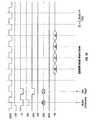
- FIG. 15is a timing diagram for a DDR SDRAM read wave form
- FIG. 16is a timing diagram for a SDRAM read wave form
- FIG. 17is a timing diagram for a DDR SDRAM write wave form
- FIG. 18is a timing diagram for a SDRAM write wave form
- FIGS. 19-21are state diagrams for the finite state machines of both the DDR SDRAM to SDRAM and SDRAM to DDR SDRAM translators.
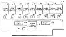
- FIG. 1is a block diagram of a 72 bit registered DDR module 10 for use in a computing device compliant with the DDR memory standard.
- DDRalso refers to the DDR SDRAM memory standard.
- the module 10is a memory module such as a DIMM or SIMM for a computing device such as a personal computer.
- the module 10is insertable into a DDR memory slot of the computing device and allows SDRAM memory on the module 10 to be used in a computing device designed for DDR memory.
- the module 10contains nine SDRAM memory chips 12 a - 12 i which are compliant with the SDRAM memory standard. Associated with each respective memory chip 12 a - 12 i is a resistor pack 14 a - 14 i which contains a network of eight resistors for each memory chip 12 a - 12 i , as is standard in a SDRAM memory system. The SDRAM memory chips 12 a - 12 i and the resistors chips 14 a - 14 i form a standard SDRAM memory array 22 .
- the module 10also includes a phase lock loop (PLL) 20 which is capable of generating an internal timing reference which is used by systems of the module 10 .
- PLLphase lock loop
- the module 10includes two general purpose registers 16 a and 16 b which are used by a DDR to SDRAM ASIC 18 in converting the signals between the computing device and the module 10 for proper functionality.
- the DDR to SDRAM ASIC 18 and registers 16form a DDR to SDRAM translator interface 24 .
- the DDR to SDRAM translator interface 24is operable to convert the control, data, and addressing signals between the computing device and the SDRAM memory chips 12 a - 12 i .
- DDR to SDRAM translator interface 24is being shown to operate on a memory module 10 , it will be recognized by those of ordinary skill in the art that the translator interface 24 can also be used on a motherboard of a computing device or in an embedded system.
- the module 10is only shown of one illustrative use for the translator interface 24 .
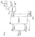
- FIG. 2is a block diagram showing the DDR to SDRAM translator interface 24 which can be used to translate signals from a SDRAM memory array 22 to a DDR (SDRAM) memory interface 26 .
- the DDR memory interface 26receive signals from the computing system.
- the DDR memory interface 26is operative to connect to a DDR memory module and provide the correct connectivity and signals between the DDR memory module and the computing system.
- the main processor for the computing systemgenerates signals at the system-side for the DDR memory.
- the processor of the computing system and the DDR memory interface 26are configured to generate signals compatible only to a DDR memory array. Therefore, the signals between the DDR memory interface 26 and the SDRAM memory array 22 need to be translated and synchronized for the SDRAM memory array 22 to function correctly.
- the read and write wave forms for DDR and SDRAM memoriesare shown in FIGS. 15-18.
- the translator interface 24includes a DDR to SDRAM ASIC (application specific integrated circuit) 18 and a register 16 .
- the DDR to SDRAM ASIC 18is a signals translator between the DDR memory interface 26 and the SDRAM memory array 22 .
- the DDR to SDRAM ASIC 18receives control signals, address signals and data signals from the DDR memory interface 26 .
- address lines addr 28 , and data bus lines dq 32are connected to the DDR to SDRAM ASIC 18 which translates them for use by the SDRAM memory array 22 .
- Address lines addr 28are translated to address lines raddr 34 for the SDRAM memory array 22
- data lines dq 32are translated to dq_out 36 .
- the SDRAM register 16is a standard register that supports custom modes of the SDRAM memory array 22 .
- the SDRAM register 16may be operative to support any low-power mode of the SDRAM memory array 22 or buffer and clock the load of SDRAM memory array 22 .
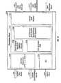
- FIG. 3a block diagram of the DDR to SDRAM ASIC 18 is shown.
- System-side DDR memory data bus and DQS signalsare connected into the DDR to SDRAM ASIC 18 by DDR DATA/DQS buses 38 .
- DDR control/address signals 40connect the system-side DDR memory control/address signals into the DDR to SDRAM ASIC 18 .
- System clock 30is also inputted into the DDR to SDRAM ASIC 18 .
- the DDR to SDRAM ASIC 18has an SSTL-II to LVTTL interface conversion 42 to provide the appropriate logic levels between the DDR memory interface 26 and SDRAM memory array 22 .
- the DDR memoryoperates using SSTL-II (stub series-terminate logic) levels wherein V DD is about 2.5V.
- regular SDRAMuses LVTTL (low voltage transistor-transistor logic) levels wherein V DD is about 3.3 V. Therefore the interface conversion 42 is operative to shift the logic levels of the incoming and outgoing signals accordingly.
- the interface conversion 42converts the interface logic of DDR SDRAM to regular SDRAM for voltage levels and interface architecture.
- the DDR to SDRAM ASIC 18further includes a translation block 44 which has a mode register and burst address decoder 46 .
- the DDR to SDRAM ASIC 18also has a synchronous dual pipeline synchronizing FIFO buffer 48 and a DQS Generator Finite State Machine 50 .
- the translation block 44provides the correct timing of signals between the DDR memory interface 26 and the SDRAM memory array 22 .
- the DDR to SDRAM ASIC 18further includes an internal SDRAM register 52 and delay lock loop (DLL) 54 for an internal system clock of the ASIC 18 .
- DLLdelay lock loop
- the mode register and burst address decoder 46converts burst lengths from the DDR memory interface 26 into burst lengths that are recognized by the SDRAM memory array 22 .
- FIG. 7a circuit for the mode register and address decoder 46 is shown.
- the decoder 46must convert the burst modes from the DDR memory interface 26 into standard SDRAM burst modes.
- the decoder 46has an encoder 700 and a first set of multiplexers 702 a - 702 c .
- the inputs to the multiplexers 702 a , 702 b , and 702 care the different burst modes “010”, “001”, and “000” for the SDRAM memory array 22 .
- the input to the encoder 700are address lines add[0], add[1] and add[2] which indicate the DDR burst mode.
- the appropriate multiplexeris enabled depending upon the burst mode indicated by the address lines add[0], add[1] and add[2].
- the output of the multiplexers 702 a - 702 care the input to a second set of multiplexers 704 a - 704 c which also have address lines add[0], add[1], and add[2] as inputs.
- the multiplexers 704 a - 704 care enabled by logically ANDING cke, cs_n, ras_n, cas_n and we_n with AND gate 706 .
- the mode register and address decoder 46further includes address latch 708 which latches address lines add[3] to add[11].
- the address lines add[3] to add[11] from the address latch 708are placed on address bus 710 , along with the outputs from the multiplexers 704 a - 704 c (i.e., mux_burst[0], mux_burst[1], and mux_burst[2].
- the bus_addr[11:0] linesare inputted into shift register 712 for use in burst mode, or inputted into multiplexer bus mux 714 .
- control signalsare fed into AND gates 718 and 720 with the result being logically OR'ed by OR gate 722 .
- the output of the bus mux multiplexer 714are address lines addr[11:0] which are fed into address latch 716 and can be accessed as raddr[11:0] 24 by the SDRAM memory array 22 .
- the FIFO buffer 48 of the ASIC 18performs bandwidth mismatch conversion to synchronize the DDR memory interface 26 and the SDRAM memory array 22 .
- the DDR memory interface 26operates at twice the bandwidth of the SDRAM memory array 22 .
- the dual pipeline FIFO buffer 48can accommodate for the frequency mismatch by storing data from the DDR memory interface 26 that cannot be immediately written or read by the SDRAM memory array 22 . Therefore the FIFO buffer 48 can synchronize the read/write cycles.
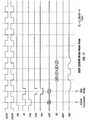
- FIG. 6a circuit diagram for the FIFO buffer 48 is shown.
- Data lines 602are inputted into buffers 604 a - 604 d .
- buffers 604 b and 604 care not shown.
- Buffer 604 astores word “0”
- buffer 604 bstores word “1”
- buffer 604 cstores word “2”
- buffer 604 dstores word “3”.
- Each buffer 604is appropriately enabled from counter 608 and 2 ⁇ 4 decoder 610 .
- the counter 608will provide a count which is decoded by the decoder 610 to enable the appropriate buffer 604 .
- the appropriate buffer 604When the appropriate buffer 604 is enabled, it's output is sent to 4 ⁇ 1 multiplexer 614 which is enabled at the appropriate timing reference signal by a second counter 612 .
- the 4 ⁇ 1 multiplexer 614can synchronize the data output for use by the SDRAM memory array 22 .
- the conversion circuit 400has a lower bit buffer 402 a and an upper bit buffer 402 b .
- Data bus D[3:0]is inputted into each buffer.
- Each bufferis enabled by a clock-in signal clk_in(dqs) which corresponds to the datastrobe dqs signal.
- FIG. 5a SDRAM to DDR bit conversion (Byte to Nibble) circuit 500 is shown.
- Eight bit data 502 from the SDRAM memory array 22is segregated into two sets for four bit data 504 a and 504 b which is inputted into multiplexer 506 .
- a select signal “Sel”enables the multiplexer 506 to output the four bit data on data bus 512 .
- the outputted four bit data 512is inputted into driver module 508 that is controlled by DQS generator FSM 50 .
- a timing signal from DLL 54is provided to the drivers 508 .
- the drivers 508are operative to output four bit data, as well as corresponding data strobe signal DQS for use by the DDR memory interface 26 .
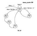
- a dqs_enb state machine diagram for the DQS generator FSM 50is shown.
- the dqs_enb state machinewill check the incoming signals (cke, cs_n, ras_n, cas_n and we_n) to detect the read signal command. If the read signal command is detected, the dqs_enb machine will generate the appropriate dqs_enb signal. Because there are three possible burst modes lengths, the dqs_enb machine will need to detect which burst mode is set and act accordingly.
- a latency counter state machine diagramis shown for the DQS generator FSM 50 .
- the latency counter state machinewill also detect the read command signal, but will also detect the latency of the device and generate a latency enable for 2 or 3 latency.
- the dqs_enb state machine(i.e., FIG. 19) will receive the latency enable signal from the latency counter FSM shown in FIG. 20 .
- FIG. 21a dqs_state_machine state diagram for the DQS generator FSM 50 is shown.
- the dqs_state_machine FSMwill generate the actual DQS (data strobe) signal based on the dqs_enb and latency_counter FSM's.
- the dqs signalcould vary in shapes based on burst mode of 2, 4, or 8.
- the DQS signalis derived from the drivers 508 based upon the DQS generator 50 , as shown in FIG. 5 .
- FIG. 8is a block diagram of a 72 bit registered SDRAM module 810 for use in a computing device compliant with the SDRAM memory standard.
- the module 810is a memory module such as a DIMM or SIMM for a computing device such as a personal computer.
- the module 810is insertable into a SDRAM memory slot of the computing device and allows DDR memory to be used in a computing device designed for SDRAM memory.
- the module 810contains nine DDR memory chips 812 a - 812 i which are compliant with the DDR memory standard. Associated with each respective memory chip 812 a - 812 i is a resistor pack 814 a - 814 i which contains a network of eight resistors for each memory chip 812 a - 812 i , as is standard in registered DDR memory systems. The DDR memory chips 812 a - 812 i and the resistor chips 814 a - 814 i form a standard DDR memory array 822 .
- the module 810also includes a phase lock loop (PLL) 820 which is capable of generating an internal timing reference which is used by systems of the module 810 .
- PLLphase lock loop
- the module 810includes two general purpose registers 816 a and 816 b which are used by a SDRAM to DDR ASIC 818 that converts the signals between the computing device and the module 810 for proper functionality.
- the SDRAM to DDR ASIC 818 and the registers 816form a SDRAM to DDR translator interface 824 .
- the SDRAM to DDR translator interface 824is operable to convert the control, data, and addressing signals between the computing device and the DDR memory chips 812 a - 812 i .
- DDR memory chips 812 a - 812 iit is possible to use DDR memory chips 812 a - 812 i in a computing device which was designed for SDRAM memory chips.
- the SDRAM to DDR translator interface 824is being shown to operate on a memory module 810 , it will be recognized by those of ordinary skill in the art that the translator interface 824 can also be used on a motherboard of a computing device or in an embedded system.
- the module 810is only shown as one illustrative use for the translator interface 824 .
- FIG. 9is a block diagram showing the SDRAM to DDR translator interface 824 which can be used to translate signals from the DDR memory array 822 to a SDRAM memory interface 926 .
- the SDRAM memory interface 926receive signals from the computing system.
- the SDRAM memory interface 926is operative to connect to a SDRAM memory module and provide the correct connectivity and signals between the SDRAM memory module and the computing system.
- the main processor for the computing systemgenerates signals at the system-side for the SDRAM memory.
- the processor of the computing system and the SDRAM memory interface 926are configured to generate signals compatible only to a SDRAM memory array. Therefore, the signals between the SDRAM memory interface 926 and the DDR memory array 822 need to be translated and synchronized for the DDR memory array 822 to function correctly.
- the translator interface 824includes a SDRAM to DDR ASIC (application specific integrated circuit) 818 and a register 816 .
- the SDRAM to DDR ASIC 818is a signals translator between the SDRAM memory interface 926 and the DDR memory array 822 .
- the SDRAM to DDR ASIC 818receives control signals, address signals and data signals from the SDRAM memory interface 926 .
- address lines addr 928 and data bus lines dq 932are connected to the SDRAM to DDR ASIC 818 which translates them for use by the DDR memory array 822 .
- Address lines addr 928are translated to address lines raddr 934
- data lines dq 932are translated to dq_out 936 .
- the DDR register 816is a standard register that supports custom modes of the DDR memory array 822 .
- the DDR register 816may be operative to support any low-power mode of the DDR memory array 822 or buffer and clock the load of DDR memory array 822 .
- FIG. 10a block diagram of the SDRAM to DDR ASIC 818 is shown.
- System-side SDRAM memory data busesare connected into the SDRAM to DDR ASIC 818 by SDRAM DATA buses 838 .
- SDRAM control/address signals 840connect the system-side SDRAM memory control/address signals into the SDRAM to DDR ASIC 818 .
- System clock 930is also inputted into the SDRAM to DDR ASIC 818 .
- the SDRAM to DDR ASIC 818has an LVTTL to SSTL-II interface conversion 1042 to provide the appropriate logic levels between the SDRAM memory interface 926 and DDR memory array 822 , as previously discussed.
- the DDR memoryoperates using SSTL-II (stub series-terminate logic) levels wherein V DD is about 2.5V.
- regular SDRAMuses LVTTL (low voltage transistor-transistor logic) levels wherein V DD is about 3.3 V. Therefore the interface conversion 1042 is operative to shift the logic levels of the incoming and outgoing signals accordingly.
- the interface conversion 1042converts the interface logic of SDRAM to regular DDR SDRAM for voltage levels and interface architecture.
- the SDRAM to DDR ASIC 818further includes a translation block 1044 which has a mode register and burst address decoder 1046 .
- the SDRAM to DDR ASIC 818also has a synchronous dual pipeline synchronizing FIFO buffer 1048 and a DQS Generator Finite State Machine 1050 .
- the translation block 1044provides the correct timing of signals between the SDRAM memory interface 926 and the DDR memory array 822 .
- the SDRAM to DDR ASIC 818further includes an internal DDR register 1052 and delay lock loop (DLL) 1054 for an internal system clock of the ASIC 818 .
- DLLdelay lock loop
- the mode register and burst address decoder 1046converts burst lengths from the SDRAM memory interface 926 into burst lengths that are recognized by the DDR memory array 822 .
- a circuit for the mode register and address decoder 1046is shown.
- the decoder 1046must convert the burst modes from the SDRAM memory interface 926 into standard DDR burst modes.
- the decoder 1046has an encoder 1400 and a first set of multiplexers 1402 a - 1402 c .
- the inputs to the multiplexers 1402 a , 1402 b , and 1402 care the different burst modes “010”, “001”, and “000” for the DDR memory array 822 .
- the input to the encoder 1400are address lines add[0], add[1] and add[2] which indicate the SDRAM burst mode.
- the appropriate multiplexeris enabled depending upon the burst mode indicated by the address lines add[0], add[1] and add[2].
- the output of the multiplexers 1402 a - 1402 care the input to a second set of multiplexers 1404 a - 1404 c which also have address lines add[0], add[1], and add[2] as inputs.
- the multiplexers 1404 a - 1404 care enabled by logically ANDING cke, cs_n, ras_n, cas_n and we_n with AND gate 1406 .
- the mode register and address decoder 1046further includes address latch 1408 which latches address lines add[3] to add[11].
- the address lines add[3] to add[11] from the address latch 1408are placed on address bus 1410 , along with the outputs from the multiplexers 1404 a - 1404 c (i.e., mux_burst[0], mux_burst[1], and mux_burst[2].
- the bus_addr[11:0] linesare inputted into shift register 1412 for use in burst mode, or multiplexer bus mux 1414 .
- control signalsare fed into AND gates 1418 and 1420 with the result being logically OR'ed by OR gate 1422 .
- the output of the multiplexer bus mux 1414are address lines addr[11:0] which are fed into address latch 1416 and can be accessed as raddr[11:0] 1424 by the DDR memory array 822 .
- the FIFO buffer 1048 of the ASIC 818performs bandwidth mismatch conversion to synchronize the SDRAM memory interface 926 and the DDR memory array 822 .
- the SDRAM memory interface 926operates at twice the bandwidth of the SDRAM memory array 822 .
- the dual pipeline FIFO buffer 1048can accommodate for the frequency mismatch by storing data from the SDRAM memory interface 926 that cannot be immediately written or read by the DDR memory array 822 . Therefore the FIFO buffer 1048 can synchronize the read/write cycles.
- a circuit diagram for the FIFO buffer 1048is shown.
- Data lines 1302are inputted into buffers 1304 a - 1304 d .
- buffers 1304 b and 1304 care not shown.
- Buffer 1304 astores word “0”
- buffer 1304 bstores word “1”
- buffer 1304 cstores word “2”
- buffer 1304 dstores word “3”.
- Each buffer 1304is appropriately enabled from counter 1308 and 2 ⁇ 4 decoder 1310 .
- the counter 1308will provide a count which is decoded by the decoder 1310 to enable the appropriate buffer 1304 .
- the 4 ⁇ 1 multiplexer 1314can synchronize the data output for use by the DDR memory array 822 .
- a DDR to SDRAM Bit conversion circuit(nibble to byte) 1100 is shown.
- the data from the SDRAM memory interface 926is eight bit data whereas the DDR memory array 822 uses four bit data. Therefore it is necessary to convert the data for proper operation.
- the conversion circuit 1100has a lower bit buffer 1102 a and an upper bit buffer 1102 b .
- Data bus D[3:0]is inputted into each buffer.
- Each bufferis enabled by a clock in signal clk_in(dqs) which corresponds to the datastrobe dqs signal.
- the eight bit SDRAM datamust be converted to four bits for the DDR memory array 822 .
- a SDRAM to DDR bit conversion (Byte to Nibble) circuit 1200is shown.
- Eight bit data 1202 from the SDRAM memory interface 926is segregated into two sets for four bit data 1204 a and 1204 b which is inputted into multiplexer 1206 .
- a select signal Selenables the multiplexer 1206 to output the four bit data on data bus 1212 .
- the outputted four bit data 1212is inputted into driver module 1208 that is controlled by DQS Generator Finite State Machine 1050 .
- a timing signal from DLL 1054is provided to the drivers 1208 .
- the drivers 1208are operative to output four bit data, as well as data strobe signal DQS for use by DDR memory array 822 .
- the DQS Generator Finite State Machine 1050is controlled using the finite state diagrams shown and explained for FIGS. 19-21.
Landscapes
- Dram (AREA)
Abstract
Description
Claims (24)
Priority Applications (3)
| Application Number | Priority Date | Filing Date | Title |
|---|---|---|---|
| US10/097,687US6707756B2 (en) | 2002-03-12 | 2002-03-12 | System and method for translation of SDRAM and DDR signals |
| PCT/US2003/007403WO2003079662A2 (en) | 2002-03-12 | 2003-03-10 | System and method for translation of sdram and ddr signals |
| AU2003218081AAU2003218081A1 (en) | 2002-03-12 | 2003-03-10 | System and method for translation of sdram and ddr signals |
Applications Claiming Priority (1)
| Application Number | Priority Date | Filing Date | Title |
|---|---|---|---|
| US10/097,687US6707756B2 (en) | 2002-03-12 | 2002-03-12 | System and method for translation of SDRAM and DDR signals |
Publications (2)
| Publication Number | Publication Date |
|---|---|
| US20030174569A1 US20030174569A1 (en) | 2003-09-18 |
| US6707756B2true US6707756B2 (en) | 2004-03-16 |
Family
ID=28039231
Family Applications (1)
| Application Number | Title | Priority Date | Filing Date |
|---|---|---|---|
| US10/097,687Expired - LifetimeUS6707756B2 (en) | 2002-03-12 | 2002-03-12 | System and method for translation of SDRAM and DDR signals |
Country Status (3)
| Country | Link |
|---|---|
| US (1) | US6707756B2 (en) |
| AU (1) | AU2003218081A1 (en) |
| WO (1) | WO2003079662A2 (en) |
Cited By (9)
| Publication number | Priority date | Publication date | Assignee | Title |
|---|---|---|---|---|
| US20040190365A1 (en)* | 2003-03-27 | 2004-09-30 | International Business Machines Corporation | Synchronous dynamic random access memory device having memory command cancel function |
| US20040199715A1 (en)* | 2003-04-01 | 2004-10-07 | International Business Machines Corporation | Method for performing a command cancel function in a dram |
| US20080101137A1 (en)* | 2001-06-29 | 2008-05-01 | Hiroshi Nakamura | Semiconductor memory device having a plurality of chips and capability of outputting a busy signal |
| US20080183916A1 (en)* | 2007-01-30 | 2008-07-31 | Mark David Bellows | Using Extreme Data Rate Memory Commands to Scrub and Refresh Double Data Rate Memory |
| US20100042778A1 (en)* | 2008-08-18 | 2010-02-18 | Advanced Micro Devices, Inc. | Memory System Such as a Dual-Inline Memory Module (DIMm) and Computer System Using the Memory System |
| US20110063931A1 (en)* | 2009-09-11 | 2011-03-17 | Avago Technologies Enterprise IP (Singapore) Pte. Ltd. | Interfaces, circuits, and methods for communicating with a double data rate memory device |
| US8279697B2 (en) | 2009-09-11 | 2012-10-02 | Avago Technologies Enterprise IP (Singapore) Pte. Ltd. | Circuits and methods for reducing noise in the power supply of circuits coupled to a bidirectional bus |
| US20130173966A1 (en)* | 2010-07-23 | 2013-07-04 | Panasonic Corporation | Memory controller and memory access system |
| US8868826B2 (en) | 2010-05-20 | 2014-10-21 | Cisco Technology, Inc. | Facilitating communication between memory devices and CPUs |
Families Citing this family (46)
| Publication number | Priority date | Publication date | Assignee | Title |
|---|---|---|---|---|
| US6742058B2 (en)* | 2002-09-27 | 2004-05-25 | Texas Instruments Incorporated | Memory controller having a multiplexer selecting either second set of input signals or converted signals from first set of input signals by a bus mode input |
| KR101377305B1 (en)* | 2005-06-24 | 2014-03-25 | 구글 인코포레이티드 | An integrated memory core and memory interface circuit |
| US8130560B1 (en) | 2006-11-13 | 2012-03-06 | Google Inc. | Multi-rank partial width memory modules |
| US8041881B2 (en) | 2006-07-31 | 2011-10-18 | Google Inc. | Memory device with emulated characteristics |
| US20080082763A1 (en) | 2006-10-02 | 2008-04-03 | Metaram, Inc. | Apparatus and method for power management of memory circuits by a system or component thereof |
| US8081474B1 (en) | 2007-12-18 | 2011-12-20 | Google Inc. | Embossed heat spreader |
| US8438328B2 (en) | 2008-02-21 | 2013-05-07 | Google Inc. | Emulation of abstracted DIMMs using abstracted DRAMs |
| US8327104B2 (en) | 2006-07-31 | 2012-12-04 | Google Inc. | Adjusting the timing of signals associated with a memory system |
| US7609567B2 (en) | 2005-06-24 | 2009-10-27 | Metaram, Inc. | System and method for simulating an aspect of a memory circuit |
| US8055833B2 (en) | 2006-10-05 | 2011-11-08 | Google Inc. | System and method for increasing capacity, performance, and flexibility of flash storage |
| US8386722B1 (en) | 2008-06-23 | 2013-02-26 | Google Inc. | Stacked DIMM memory interface |
| US9171585B2 (en) | 2005-06-24 | 2015-10-27 | Google Inc. | Configurable memory circuit system and method |
| US8111566B1 (en) | 2007-11-16 | 2012-02-07 | Google, Inc. | Optimal channel design for memory devices for providing a high-speed memory interface |
| US8077535B2 (en) | 2006-07-31 | 2011-12-13 | Google Inc. | Memory refresh apparatus and method |
| US8397013B1 (en) | 2006-10-05 | 2013-03-12 | Google Inc. | Hybrid memory module |
| US10013371B2 (en) | 2005-06-24 | 2018-07-03 | Google Llc | Configurable memory circuit system and method |
| US8060774B2 (en) | 2005-06-24 | 2011-11-15 | Google Inc. | Memory systems and memory modules |
| US8335894B1 (en) | 2008-07-25 | 2012-12-18 | Google Inc. | Configurable memory system with interface circuit |
| US20080028136A1 (en) | 2006-07-31 | 2008-01-31 | Schakel Keith R | Method and apparatus for refresh management of memory modules |
| US9507739B2 (en) | 2005-06-24 | 2016-11-29 | Google Inc. | Configurable memory circuit system and method |
| US8796830B1 (en) | 2006-09-01 | 2014-08-05 | Google Inc. | Stackable low-profile lead frame package |
| US7386656B2 (en) | 2006-07-31 | 2008-06-10 | Metaram, Inc. | Interface circuit system and method for performing power management operations in conjunction with only a portion of a memory circuit |
| US8244971B2 (en) | 2006-07-31 | 2012-08-14 | Google Inc. | Memory circuit system and method |
| US8359187B2 (en) | 2005-06-24 | 2013-01-22 | Google Inc. | Simulating a different number of memory circuit devices |
| US8089795B2 (en) | 2006-02-09 | 2012-01-03 | Google Inc. | Memory module with memory stack and interface with enhanced capabilities |
| WO2007028109A2 (en) | 2005-09-02 | 2007-03-08 | Metaram, Inc. | Methods and apparatus of stacking drams |
| US9632929B2 (en) | 2006-02-09 | 2017-04-25 | Google Inc. | Translating an address associated with a command communicated between a system and memory circuits |
| US8074022B2 (en) | 2006-09-28 | 2011-12-06 | Virident Systems, Inc. | Programmable heterogeneous memory controllers for main memory with different memory modules |
| US9984012B2 (en) | 2006-09-28 | 2018-05-29 | Virident Systems, Llc | Read writeable randomly accessible non-volatile memory modules |
| US20080082750A1 (en)* | 2006-09-28 | 2008-04-03 | Okin Kenneth A | Methods of communicating to, memory modules in a memory channel |
| US7761624B2 (en)* | 2006-09-28 | 2010-07-20 | Virident Systems, Inc. | Systems and apparatus for main memory with non-volatile type memory modules, and related technologies |
| US7761623B2 (en)* | 2006-09-28 | 2010-07-20 | Virident Systems, Inc. | Main memory in a system with a memory controller configured to control access to non-volatile memory, and related technologies |
| US8949555B1 (en) | 2007-08-30 | 2015-02-03 | Virident Systems, Inc. | Methods for sustained read and write performance with non-volatile memory |
| WO2008040028A2 (en)* | 2006-09-28 | 2008-04-03 | Virident Systems, Inc. | Systems, methods, and apparatus with programmable memory control for heterogeneous main memory |
| US7761626B2 (en)* | 2006-09-28 | 2010-07-20 | Virident Systems, Inc. | Methods for main memory in a system with a memory controller configured to control access to non-volatile memory, and related technologies |
| US7761625B2 (en)* | 2006-09-28 | 2010-07-20 | Virident Systems, Inc. | Methods for main memory with non-volatile type memory modules, and related technologies |
| WO2008051940A2 (en)* | 2006-10-23 | 2008-05-02 | Virident Systems, Inc. | Methods and apparatus of dual inline memory modules for flash memory |
| JP2008299476A (en) | 2007-05-30 | 2008-12-11 | Fujitsu Microelectronics Ltd | Semiconductor integrated circuit |
| US9921896B2 (en) | 2007-08-30 | 2018-03-20 | Virident Systems, Llc | Shutdowns and data recovery to avoid read errors weak pages in a non-volatile memory system |
| US8417873B1 (en) | 2008-06-24 | 2013-04-09 | Virident Systems, Inc. | Random read and read/write block accessible memory |
| US9513695B2 (en) | 2008-06-24 | 2016-12-06 | Virident Systems, Inc. | Methods of managing power in network computer systems |
| US8595398B2 (en)* | 2009-03-09 | 2013-11-26 | Cypress Semiconductor Corp. | Multi-port memory devices and methods |
| US9489326B1 (en)* | 2009-03-09 | 2016-11-08 | Cypress Semiconductor Corporation | Multi-port integrated circuit devices and methods |
| DE202010017690U1 (en) | 2009-06-09 | 2012-05-29 | Google, Inc. | Programming dimming terminating resistor values |
| EP3020047A1 (en)* | 2013-07-09 | 2016-05-18 | Hewlett Packard Enterprise Development LP | Write flow control for memory modules that include or interface with non-compliant memory technologies |
| CN108230537B (en)* | 2017-12-29 | 2020-08-18 | 深圳怡化电脑股份有限公司 | Image data processing method, device, equipment and storage medium |
Citations (3)
| Publication number | Priority date | Publication date | Assignee | Title |
|---|---|---|---|---|
| US6392946B1 (en)* | 2001-05-15 | 2002-05-21 | Leadtek Research Inc. | SDR and QDR converter and interface card, motherboard and memory module interface using the same |
| US6501671B2 (en)* | 2000-06-30 | 2002-12-31 | Mitsubishi Denki Kabushiki Kaisha | Semiconductor memory device enabling selective production of different semiconductor memory devices operating at different external power-supply voltages |
| US6507888B2 (en)* | 2001-01-03 | 2003-01-14 | Leadtek Research Inc. | SDR and DDR conversion device and associated interface card, main board and memory module interface |
Family Cites Families (2)
| Publication number | Priority date | Publication date | Assignee | Title |
|---|---|---|---|---|
| US6044032A (en)* | 1998-12-03 | 2000-03-28 | Micron Technology, Inc. | Addressing scheme for a double data rate SDRAM |
| KR100304963B1 (en)* | 1998-12-29 | 2001-09-24 | 김영환 | Semiconductor memory |
- 2002
- 2002-03-12USUS10/097,687patent/US6707756B2/ennot_activeExpired - Lifetime
- 2003
- 2003-03-10AUAU2003218081Apatent/AU2003218081A1/ennot_activeAbandoned
- 2003-03-10WOPCT/US2003/007403patent/WO2003079662A2/ennot_activeApplication Discontinuation
Patent Citations (3)
| Publication number | Priority date | Publication date | Assignee | Title |
|---|---|---|---|---|
| US6501671B2 (en)* | 2000-06-30 | 2002-12-31 | Mitsubishi Denki Kabushiki Kaisha | Semiconductor memory device enabling selective production of different semiconductor memory devices operating at different external power-supply voltages |
| US6507888B2 (en)* | 2001-01-03 | 2003-01-14 | Leadtek Research Inc. | SDR and DDR conversion device and associated interface card, main board and memory module interface |
| US6392946B1 (en)* | 2001-05-15 | 2002-05-21 | Leadtek Research Inc. | SDR and QDR converter and interface card, motherboard and memory module interface using the same |
Cited By (17)
| Publication number | Priority date | Publication date | Assignee | Title |
|---|---|---|---|---|
| US20080101137A1 (en)* | 2001-06-29 | 2008-05-01 | Hiroshi Nakamura | Semiconductor memory device having a plurality of chips and capability of outputting a busy signal |
| US7663967B2 (en)* | 2001-06-29 | 2010-02-16 | Kabushiki Kaisha Toshiba | Semiconductor memory device having a plurality of chips and capability of outputting a busy signal |
| US6826113B2 (en)* | 2003-03-27 | 2004-11-30 | International Business Machines Corporation | Synchronous dynamic random access memory device having memory command cancel function |
| US20040190365A1 (en)* | 2003-03-27 | 2004-09-30 | International Business Machines Corporation | Synchronous dynamic random access memory device having memory command cancel function |
| US20040199715A1 (en)* | 2003-04-01 | 2004-10-07 | International Business Machines Corporation | Method for performing a command cancel function in a dram |
| US7480774B2 (en)* | 2003-04-01 | 2009-01-20 | International Business Machines Corporation | Method for performing a command cancel function in a DRAM |
| US20080183916A1 (en)* | 2007-01-30 | 2008-07-31 | Mark David Bellows | Using Extreme Data Rate Memory Commands to Scrub and Refresh Double Data Rate Memory |
| US8054676B2 (en)* | 2008-08-18 | 2011-11-08 | Advanced Micro Devices, Inc. | Memory system such as a dual-inline memory module (DIMM) and computer system using the memory system |
| US20100042778A1 (en)* | 2008-08-18 | 2010-02-18 | Advanced Micro Devices, Inc. | Memory System Such as a Dual-Inline Memory Module (DIMm) and Computer System Using the Memory System |
| US20110063931A1 (en)* | 2009-09-11 | 2011-03-17 | Avago Technologies Enterprise IP (Singapore) Pte. Ltd. | Interfaces, circuits, and methods for communicating with a double data rate memory device |
| US8234422B2 (en)* | 2009-09-11 | 2012-07-31 | Avago Technologies Enterprise IP (Singapore) Pte. Ltd | Interfaces, circuits, and methods for communicating with a double data rate memory device |
| US8279697B2 (en) | 2009-09-11 | 2012-10-02 | Avago Technologies Enterprise IP (Singapore) Pte. Ltd. | Circuits and methods for reducing noise in the power supply of circuits coupled to a bidirectional bus |
| US8868826B2 (en) | 2010-05-20 | 2014-10-21 | Cisco Technology, Inc. | Facilitating communication between memory devices and CPUs |
| US9514791B2 (en) | 2010-05-20 | 2016-12-06 | Cisco Technology, Inc. | Facilitating communication between memory devices of different technologies |
| US10083133B2 (en) | 2010-05-20 | 2018-09-25 | Cisco Technology, Inc. | Facilitating communication between memory devices and CPUs |
| US20130173966A1 (en)* | 2010-07-23 | 2013-07-04 | Panasonic Corporation | Memory controller and memory access system |
| US8972790B2 (en)* | 2010-07-23 | 2015-03-03 | Panasonic Intellectual Property Management Co., Ltd. | Memory controller and memory access system with error detection using data comparison of loop-backed signals |
Also Published As
| Publication number | Publication date |
|---|---|
| WO2003079662A2 (en) | 2003-09-25 |
| WO2003079662A3 (en) | 2003-12-18 |
| AU2003218081A1 (en) | 2003-09-29 |
| AU2003218081A8 (en) | 2003-09-29 |
| US20030174569A1 (en) | 2003-09-18 |
| WO2003079662A9 (en) | 2004-02-12 |
Similar Documents
| Publication | Publication Date | Title |
|---|---|---|
| US6707756B2 (en) | System and method for translation of SDRAM and DDR signals | |
| US6763416B1 (en) | Capturing read data | |
| US8705313B2 (en) | DDR PSRAM and data writing and reading methods thereof | |
| US7447095B2 (en) | Multi-port memory device | |
| JP5241780B2 (en) | Synchronous memory read data collection | |
| US7443760B2 (en) | Multi-port memory device with serial input/output interface | |
| US7835219B2 (en) | Multi-port memory device | |
| JPH08227394A (en) | Data-processing system and its operating method | |
| JP2009507431A (en) | Method and apparatus for converting parallel data to serial data in high speed applications | |
| US8406080B2 (en) | Data output control circuit of a double data rate (DDR) synchronous semiconductor memory device responsive to a delay locked loop (DLL) clock and method thereof | |
| JP3334589B2 (en) | Signal delay device and semiconductor memory device | |
| US8737145B2 (en) | Semiconductor memory device for transferring data at high speed | |
| US20090254699A1 (en) | Synchronous dynamic random access memory interface and method | |
| US8593902B2 (en) | Controller and access method for DDR PSRAM and operating method thereof | |
| US20180343015A1 (en) | Systems and methods for multi-stage data serialization in a memory system | |
| US7974145B2 (en) | Semiconductor memory device using bus inversion scheme | |
| US7212449B2 (en) | Data output device of semiconductor memory device | |
| US8429319B2 (en) | Multi-port memory device with serial input/output interface | |
| US6044474A (en) | Memory controller with buffered CAS/RAS external synchronization capability for reducing the effects of clock-to-signal skew | |
| US20230326504A1 (en) | Semiconductor devices capable of performing write training without read training, and memory system including the same |
Legal Events
| Date | Code | Title | Description |
|---|---|---|---|
| AS | Assignment | Owner name:SMART MODULAR TECHNOLOGIES, INC., CALIFORNIA Free format text:ASSIGNMENT OF ASSIGNORS INTEREST;ASSIGNOR:AMIDI, HOSSEIN;REEL/FRAME:012700/0082 Effective date:20020308 | |
| STCF | Information on status: patent grant | Free format text:PATENTED CASE | |
| AS | Assignment | Owner name:WELLS FARGO FOOTHILL, INC., CALIFORNIA Free format text:ASSIGNMENT OF ASSIGNORS INTEREST;ASSIGNOR:SMART MODULAR TECHNOLOGIES, INC., A CALIFORNIA CORPORATION;REEL/FRAME:015302/0974 Effective date:20040416 | |
| CC | Certificate of correction | ||
| AS | Assignment | Owner name:U.S. BANK NATIONAL ASSOCIATION, AS TRUSTEE, MINNES Free format text:COLLATERAL ASSIGNMENT OF PATENTS (SECURITY AGREEMENT);ASSIGNOR:SMART MODULAR TECHNOLOGIES, INC.;REEL/FRAME:015829/0808 Effective date:20050328 | |
| FEPP | Fee payment procedure | Free format text:PAYOR NUMBER ASSIGNED (ORIGINAL EVENT CODE: ASPN); ENTITY STATUS OF PATENT OWNER: LARGE ENTITY | |
| FPAY | Fee payment | Year of fee payment:4 | |
| REMI | Maintenance fee reminder mailed | ||
| AS | Assignment | Owner name:SMART MODULAR TECHNOLOGIES, INC., CALIFORNIA Free format text:RELEASE OF SECURITY INTEREST RECORDED AT REEL/FRAME (015829/0808);ASSIGNOR:U.S. BANK NATIONAL ASSOCIATION;REEL/FRAME:026811/0093 Effective date:20110825 Owner name:SMART MODULAR TECHNOLOGIES, INC., CALIFORNIA Free format text:RELEASE OF SECURITY INTERESTS RECORDED AT REEL/FRAMES (015302/0974); (015931/0509); & (015312/0001);ASSIGNOR:WELLS FARGO BANK, NATIONAL ASSOCIATION, AS SUCCESSOR AGENT;REEL/FRAME:026811/0087 Effective date:20110825 | |
| FPAY | Fee payment | Year of fee payment:8 | |
| AS | Assignment | Owner name:BARCLAYS BANK PLC, AS ADMINISTRATIVE AGENT, NEW YO Free format text:SECURITY AGREEMENT;ASSIGNOR:SMART MODULAR TECHNOLOGIES, INC.;REEL/FRAME:034036/0779 Effective date:20141022 | |
| FPAY | Fee payment | Year of fee payment:12 | |
| AS | Assignment | Owner name:BANK OF AMERICA, N.A., AS AGENT, CALIFORNIA Free format text:SECURITY INTEREST;ASSIGNOR:SMART MODULAR TECHNOLOGIES, INC.;REEL/FRAME:054738/0855 Effective date:20201223 | |
| AS | Assignment | Owner name:CITIZENS BANK, N.A., MASSACHUSETTS Free format text:SECURITY INTEREST;ASSIGNORS:SMART MODULAR TECHNOLOGIES, INC.;SMART HIGH RELIABILITY SOLUTIONS, LLC;SMART EMBEDDED COMPUTING, INC.;AND OTHERS;REEL/FRAME:058983/0001 Effective date:20220207 Owner name:SMART MODULAR TECHNOLOGIES, INC., CALIFORNIA Free format text:RELEASE OF SECURITY INTEREST AT REEL 034036 FRAME 0779;ASSIGNOR:BARCLAYS BANK PLC;REEL/FRAME:058960/0876 Effective date:20220107 Owner name:SMART MODULAR TECHNOLOGIES, INC., CALIFORNIA Free format text:RELEASE BY SECURED PARTY;ASSIGNOR:BANK OF AMERICA, N.A., AS AGENT;REEL/FRAME:058913/0385 Effective date:20220207 | |
| AS | Assignment | Owner name:SMART MODULAR TECHNOLOGIES, INC., CALIFORNIA Free format text:RELEASE OF PATENT SECURITY INTEREST RECORDED AT R/F 058983/0001;ASSIGNOR:CITIZENS BANK, N.A.;REEL/FRAME:071725/0207 Effective date:20250624 Owner name:SMART EMBEDDED COMPUTING, INC., ARIZONA Free format text:RELEASE OF PATENT SECURITY INTEREST RECORDED AT R/F 058983/0001;ASSIGNOR:CITIZENS BANK, N.A.;REEL/FRAME:071725/0207 Effective date:20250624 Owner name:SMART HIGH RELIABILITY SOLUTIONS LLC, CALIFORNIA Free format text:RELEASE OF PATENT SECURITY INTEREST RECORDED AT R/F 058983/0001;ASSIGNOR:CITIZENS BANK, N.A.;REEL/FRAME:071725/0207 Effective date:20250624 Owner name:CREELED, INC., CALIFORNIA Free format text:RELEASE OF PATENT SECURITY INTEREST RECORDED AT R/F 058983/0001;ASSIGNOR:CITIZENS BANK, N.A.;REEL/FRAME:071725/0207 Effective date:20250624 |