US6707083B1 - Magnetic tunneling junction with improved power consumption - Google Patents
Magnetic tunneling junction with improved power consumptionDownload PDFInfo
- Publication number
- US6707083B1 US6707083B1US10/192,458US19245802AUS6707083B1US 6707083 B1US6707083 B1US 6707083B1US 19245802 AUS19245802 AUS 19245802AUS 6707083 B1US6707083 B1US 6707083B1
- Authority
- US
- United States
- Prior art keywords
- layer
- tab
- adjacent
- magnetic tunneling
- tunneling junction
- Prior art date
- Legal status (The legal status is an assumption and is not a legal conclusion. Google has not performed a legal analysis and makes no representation as to the accuracy of the status listed.)
- Expired - Lifetime
Links
- 230000005291magnetic effectEffects0.000titleclaimsabstractdescription87
- 230000005641tunnelingEffects0.000titleclaimsabstractdescription69
- 230000005294ferromagnetic effectEffects0.000claimsabstractdescription80
- 230000004888barrier functionEffects0.000claimsabstractdescription25
- 238000000034methodMethods0.000claimsabstractdescription25
- 239000012212insulatorSubstances0.000claimsabstractdescription9
- 230000015654memoryEffects0.000claimsdescription18
- 230000005415magnetizationEffects0.000description18
- 239000010949copperSubstances0.000description8
- 238000010586diagramMethods0.000description8
- 230000004907fluxEffects0.000description6
- 230000001419dependent effectEffects0.000description5
- 239000000463materialSubstances0.000description5
- RYGMFSIKBFXOCR-UHFFFAOYSA-NCopperChemical compound[Cu]RYGMFSIKBFXOCR-UHFFFAOYSA-N0.000description4
- 230000005290antiferromagnetic effectEffects0.000description4
- 229910045601alloyInorganic materials0.000description3
- 239000000956alloySubstances0.000description3
- 239000000969carrierSubstances0.000description3
- 239000012141concentrateSubstances0.000description3
- 229910000889permalloyInorganic materials0.000description3
- 229910001030Iron–nickel alloyInorganic materials0.000description2
- VYPSYNLAJGMNEJ-UHFFFAOYSA-NSilicium dioxideChemical compoundO=[Si]=OVYPSYNLAJGMNEJ-UHFFFAOYSA-N0.000description2
- 229910052802copperInorganic materials0.000description2
- 239000003302ferromagnetic materialSubstances0.000description2
- 238000007737ion beam depositionMethods0.000description2
- 239000000696magnetic materialSubstances0.000description2
- 238000004519manufacturing processMethods0.000description2
- 238000012986modificationMethods0.000description2
- 230000004048modificationEffects0.000description2
- 230000015572biosynthetic processEffects0.000description1
- LYLITXREHOKIEO-UHFFFAOYSA-Nchromium cobalt zirconiumChemical compound[Co][Cr][Zr]LYLITXREHOKIEO-UHFFFAOYSA-N0.000description1
- 229910052681coesiteInorganic materials0.000description1
- 239000004020conductorSubstances0.000description1
- 229910052906cristobaliteInorganic materials0.000description1
- 230000003247decreasing effectEffects0.000description1
- 238000000151depositionMethods0.000description1
- 230000008021depositionEffects0.000description1
- 230000006870functionEffects0.000description1
- 230000006872improvementEffects0.000description1
- 238000009413insulationMethods0.000description1
- 238000005240physical vapour depositionMethods0.000description1
- 238000007747platingMethods0.000description1
- 230000004044responseEffects0.000description1
- 239000000377silicon dioxideSubstances0.000description1
- 238000004544sputter depositionMethods0.000description1
- 238000000992sputter etchingMethods0.000description1
- 229910052682stishoviteInorganic materials0.000description1
- 239000000126substanceSubstances0.000description1
- 229910052905tridymiteInorganic materials0.000description1
Images


Classifications
- G—PHYSICS
- G11—INFORMATION STORAGE
- G11C—STATIC STORES
- G11C11/00—Digital stores characterised by the use of particular electric or magnetic storage elements; Storage elements therefor
- G11C11/02—Digital stores characterised by the use of particular electric or magnetic storage elements; Storage elements therefor using magnetic elements
- G11C11/16—Digital stores characterised by the use of particular electric or magnetic storage elements; Storage elements therefor using magnetic elements using elements in which the storage effect is based on magnetic spin effect
- H—ELECTRICITY
- H10—SEMICONDUCTOR DEVICES; ELECTRIC SOLID-STATE DEVICES NOT OTHERWISE PROVIDED FOR
- H10B—ELECTRONIC MEMORY DEVICES
- H10B61/00—Magnetic memory devices, e.g. magnetoresistive RAM [MRAM] devices
Definitions
- the present inventionrelates to magnetic system, and more particularly to a method and system for providing magnetic tunneling junctions having improved reliability.
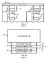
- FIG. 1depicts a portion of a conventional magnetic memory, a conventional MRAM 1 .
- the conventional MRAM 1includes MTJs 10 .
- Each MTJ 10includes at least a conventional pinned layer 20 , a conventional barrier layer 30 and a conventional free layer 40 .
- the conventional barrier layer 30is typically an insulator that serves as a tunneling barrier between the conventional pinned layer 20 and the conventional free layer 40 .
- the conventional pinned layer 20 and the conventional free layer 40are ferromagnetic.
- the magnetization of the conventional pinned layer 20is pinned in a particular direction, generally by an anitiferromagnetic layer (not shown).
- the magnetization of the conventional free layer 40is free to rotate in response to an external field.
- the conventional MRAM 1includes a conventional bit line 60 and a conventional bottom lead 50 .
- Current through the MTJ 10is carried by the conventional bit line 60 and the conventional bottom lead 50 .
- the magnetic MTJ 10is switched using a combination of current driven through the bit line 60 and the magnetic tunneling junction 10 and the current through the corresponding digit line 70 .
- FIG. 2is a diagram of a cross-sectional view of a portion of the magnetic memory 1 .
- a magnetic tunneling junction 10 having the pinned layer 20 , barrier layer 30 and free layer 40are shown.
- the magnetic tunneling junction 10is surrounded by an insulator (not explicitly shown).
- the magnetic tunneling junctiontypically includes an antiferromagnetic layer (not shown) and other layers, such as seed and/or capping layers.
- the bit line 60is typically composed of a nonmagnetic conductive material, such as Cu. In order to switch the direction of magnetization of the magnetization of the free layer 40 , current is driven through the bit line 60 and the digit line 70 (not shown in FIG. 2 ).
- the conventional MRAM 1functions, one of ordinary skill in the art will readily recognize that the conventional MRAM 1 consumes a great deal of power. In particular, a relatively large current is required in order to switch the magnetization of the free layer. As a result, a large amount of power is also consumed in order to switch the magnetization of the free layer 40 . Consequently, the MRAM 1 utilizes a large amount of power when programming an MTJ 10 .
- the present inventionprovides a method and system for providing a magnetic tunneling junction.
- the method and systemcomprise providing a free layer, a pinned layer, and a barrier between the free layer and the pinned layer.
- the free layer and the pinned layerare ferromagnetic.
- the barrier layeris an insulator.
- the magnetic tunneling junctionis coupled to a bit line.
- the bit lineincludes a ferromagnetic liner and a nonmagnetic core.
- the nonmagnetic coreincludes a top, a bottom and sides.
- the ferromagnetic linerincludes at least one tab and is adjacent to the sides and a portion of the bottom of the nonmagnetic core. The at least one tab is adjacent to the portion of the bottom of the nonmagnetic core.
- the present inventionprovides a magnetic tunneling junction that can be programmed using less power.
- FIG. 1is a diagram of a conventional memory array using conventional magnetic tunneling junctions.
- FIG. 2is a diagram of a cross section of a portion of the conventional magnetic memory including the digit lines and
- FIG. 3is a diagram of one embodiment of a magnetic tunneling junction using a first embodiment of a bit line in accordance with the present invention.
- FIG. 4is a diagram of one embodiment of a magnetic tunneling junction using a second embodiment of a bit line in accordance with the present invention.
- FIG. 5is a diagram of one embodiment of a magnetic tunneling junction using a third embodiment of a bit line in accordance with the present invention.
- FIG. 6is a high-level flow chart of one embodiment of a method in accordance with the present invention.
- FIGS. 7A-7Hdepict one embodiment of a magnetic tunneling junction using the first embodiment of a bit line in accordance with the present invention during fabrication.
- the present inventionrelates to an improvement in spin dependent tunneling sensors.
- the following descriptionis presented to enable one of ordinary skill in the art to make and use the invention and is provided in the context of a patent application and its requirements.
- Various modifications to the preferred embodimentwill be readily apparent to those skilled in the art and the generic principles herein may be applied to other embodiments.
- the present inventionis not intended to be limited to the embodiment shown, but is to be accorded the widest scope consistent with the principles and features described herein.
- the present inventionprovides a method and system for providing a magnetic tunneling junction.
- the method and systemcomprise providing a free layer, a pinned layer, and a barrier between the free layer and the pinned layer.
- the free layer and the pinned layerare ferromagnetic.
- the barrier layeris an insulator.
- the magnetic tunneling junctionis coupled to a bit line.
- the bit lineincludes a ferromagnetic liner and a nonmagnetic core.
- the nonmagnetic coreincludes a top, a bottom and sides.
- the ferromagnetic linerincludes at least one tab and is adjacent to the sides and a portion of the bottom of the nonmagnetic core. The at least one tab is adjacent to the portion of the bottom of the nonmagnetic core.
- the present inventionwill be described in terms of a particular spin-dependent tunneling sensor using particular materials and having particular components. However, one of ordinary skill in the art will readily recognize that this method and system will operate effectively for other spin-dependent tunneling sensors using other materials and having other and/or different components that are consistent with the present invention.
- the present inventionis also described in the context of a particular magnetic memory. However, one of ordinary skill in the art will readily realize that the present invention is consistent with other memories utilizing spin-dependent tunneling sensors for storing data.
- FIG. 3depicting one embodiment of a magnetic tunneling junction 10 utilizing a first embodiment of a bit line 100 in accordance with the present invention.
- the magnetic tunneling junction 10includes a pinned layer 20 , a barrier layer 30 and a free layer 40 .
- the pinned layer 20 and the free layer 40are ferromagnetic.
- the pinned layer 20 and/or the free layer 40may be synthetic. Other layers may also be synthetic, multilayers, alloys or other materials.
- the pinned layer 20has its magnetization substantially fixed, while the magnetization of the free layer 40 can respond to an applied magnetic field.
- the magnetization of the pinned layer 20is fixed using an antiferromagnetic layer (not shown) grown on an appropriate seed layer (not shown).
- the barrier layer 30is an insulating layer sufficiently thin to allow the tunneling of current carriers between the pinned layer 20 and the free layer 40 .
- the magnetic tunneling junction 10is preferably grown on a bottom lead 50 .
- the bit line 100preferably resides on the magnetic tunneling junction 10 .
- the bit line 100includes a nonmagnetic core 110 and a ferromagnetic liner 120 .
- the nonmagnetic core 110includes a liner such as Cu.
- the ferromagnetic liner 120is preferably a soft ferromagnetic liner 120 .
- the soft ferromagnetic liner 120has a low coercivity.
- the soft ferromagnetic liner 120may include Permalloy or CZC (Cobalt-zirconium-chromium).
- the first embodiment of the soft ferromagnetic liner 120extends around the sides and top of the nonmagnetic core 110 .
- the cross section of the soft ferromagnetic liner 120is essentially a horseshoe magnet.
- the soft ferromagnetic liner 120includes tabs 122 and 124 that extend across a portion of the bottom of the nonmagnetic core 110 .
- the thickness of the soft ferromagnetic liner 120is approximately thirty to fifty Angstroms, but depends upon the design of the bit line 100 .
- the soft ferromagnetic liner 120is the thinnest possible that provides the desired performance of the bit line 100 .
- the tabs 122 and 124are preferably between 0.01 and twenty percent of the width of the bit line, L. In the embodiment 100 of the bit line, the tabs 122 and 124 are adjacent to the free layer 40 . Thus, the end of the tabs 122 and 124 may abut the ends of the free layer 40 , as shown in FIG. 3 .
- the soft ferromagnetic liner 120concentrates the flux due to a current driven through the bit line 100 . As a result, less current is required to be driven through the bit line 100 to switch the magnetization of the free layer 40 .
- the tabs 122 and 124reduce the gap between the soft ferromagnetic liner 120 and the free layer 40 of the magnetic tunneling junction 10 . Consequently, the leakage of magnetic flux is further reduced by the tabs 122 and 124 .
- the current required to be driven through the bit line 100 during writingis, therefore, further reduced. Consequently, power consumption of a magnetic memory using the bit line 100 in the write mode is further reduced.
- FIG. 4is a diagram of one embodiment of a magnetic tunneling junction 10 using a second embodiment of a bit line 100 ′ in accordance with the present invention.
- the magnetic tunneling junction 10includes a pinned layer 20 , a barrier layer 30 and a free layer 40 .
- the pinned layer 20 and the free layer 40are ferromagnetic.
- the pinned layer 20 and/or the free layer 40may be synthetic. Other layers may also be synthetic, multilayers, alloys or other materials.
- the pinned layer 20has its magnetization substantially fixed, while the magnetization of the free layer 40 can respond to an applied magnetic field. Generally, the magnetization of the pinned layer 20 is fixed using an antiferromagnetic layer (not shown) grown on an appropriate seed layer (not shown).
- the barrier layer 30is an insulating layer sufficiently thin to allow the tunneling of current carriers between the pinned layer 20 and the free layer 40 .
- the magnetic tunneling junction 10is preferably grown on a bottom lead 50 .
- the bit line 100 ′preferably resides on the magnetic tunneling junction 10 .
- the bit line 100 ′includes a nonmagnetic core 110 ′ and a ferromagnetic liner 120 ′.
- the nonmagnetic core 110 ′includes a liner such as Cu.
- the ferromagnetic liner 120 ′is preferably a soft ferromagnetic liner 120 ′.
- the soft ferromagnetic liner 120 ′has a low coercivity.
- the soft ferromagnetic liner 120 ′may include Permalloy or CZC.
- the first embodiment of the soft ferromagnetic liner 120 ′extends around the sides and top of the nonmagnetic core 110 ′.
- the cross section of the soft ferromagnetic liner 120 ′is essentially a horseshoe magnet.
- the soft ferromagnetic liner 120 ′includes tabs 122 ′ and 124 ′ that extend across a portion of the bottom of the nonmagnetic core 110 ′.
- the thickness of the soft ferromagnetic liner 120 ′is approximately thirty to fifty Angstroms, but depends upon the design of the bit line 100 ′.
- the soft ferromagnetic liner 120 ′is the thinnest possible that provides the desired performance of the bit line 100 ′.
- the tabs 122 ′ and 124 ′are preferably between 0.01 and twenty percent of the width of the bit line, L.
- the ends of the tabs 122 and 124lie outside of the free layer 40 .
- the end of the tabs 122 ′ and 124 ′are not adjacent to the free layer 40 .
- the tabs 122 ′ and 124 ′lie at the outer edge of the bit line 100 ′.
- the soft ferromagnetic liner 120 ′concentrates the flux due to a current driven through the bit line 100 ′. As a result, less current is required to be driven through the bit line 100 ′ to switch the magnetization of the free layer 40 .
- the tabs 122 ′ and 124 ′reduce the gap between the soft ferromagnetic liner 120 ′ and the free layer 40 of the magnetic tunneling junction 10 . Consequently, the leakage of magnetic flux is further reduced by the tabs 122 ′ and 124 ′.
- the current required to be driven through the bit line 100 ′ during writingis, therefore, further reduced. Consequently, power consumption of a magnetic memory using the bit line 100 ′ in the write mode is further reduced.
- FIG. 5is a diagram of one embodiment of a magnetic tunneling junction using a third embodiment of a bit line 100 ′′ in accordance with the present invention.
- the magnetic tunneling junction 10includes a pinned layer 20 , a barrier layer 30 and a free layer 40 .
- the pinned layer 20 and the free layer 40are ferromagnetic.
- the pinned layer 20 and/or the free layer 40may be synthetic. Other layers may also be synthetic, multilayers, alloys or other materials.
- the pinned layer 20has its magnetization substantially fixed, while the magnetization of the free layer 40 can respond to an applied magnetic field. Generally, the magnetization of the pinned layer 20 is fixed using an antiferromagnetic layer (not shown) grown on an appropriate seed layer (not shown).
- the barrier layer 30is an insulation layer sufficiently thin to allow the tunneling of current carriers between the pinned layer 20 and the free layer 40 .
- the magnetic tunneling junction 10is preferably grown on a bottom lead 50 .
- the bit line 100 ′′preferably resides on the magnetic tunneling junction 10 .
- the bit line 100 ′′includes a nonmagnetic core 110 ′′ and a ferromagnetic liner 120 ′′.
- the nonmagnetic core 110 ′′includes a liner such as Cu.
- the ferromagnetic liner 120 ′′is preferably a soft ferromagnetic liner 120 ′′.
- the soft ferromagnetic liner 120 ′′has a low coercivity.
- the soft ferromagnetic liner 120 ′′may include Permalloy or CZC.
- the first embodiment of the soft ferromagnetic liner 120 ′′extends around the sides of the nonmagnetic core 110 ′′.
- the cross section of the soft ferromagnetic liner 120 ′′is, therefore, not a horseshoe magnet.
- the soft ferromagnetic liner 120 ′′includes tabs 122 ′′ and 124 ′′ that extend across a portion of the bottom of the nonmagnetic core 110 ′′.
- the thickness of the soft ferromagnetic liner 120 ′′is approximately thirty to fifty Angstroms, but depends upon the design of the bit line 100 ′′.
- the soft ferromagnetic liner 120 ′′is the thinnest possible that provides the desired performance of the bit line 100 ′′.
- the tabs 122 ′′ and 124 ′′are preferably between 0.01 and twenty percent of the width of the bit line, L.
- the tabs 122 ′′ and 124 ′′are adjacent to the free layer 40 .
- the end of the tabs 122 ′′ and 124 ′′may abut the ends of the free layer 40 , as shown in FIG. 5 .
- the ends of the tables 122 ′′ and 124 ′′are nearer to the outer edges of the bit line 100 ′′, not adjacent to the edges of the free layer 40 .
- the soft ferromagnetic liner 120 ′′concentrates the flux due to a current driven through the bit line 100 ′′. As a result, less current is required to be driven through the bit line 100 ′′ to switch the magnetization of the free layer 40 .
- the tabs 122 ′′ and 124 ′′reduce the gap between the soft ferromagnetic liner 120 ′′ and the free layer 40 of the magnetic tunneling junction 10 . Consequently, the leakage of magnetic flux is further reduced by the tabs 122 ′′ and 124 ′′.
- the current required to be driven through the bit line 100 ′′ during writingis, therefore, further reduced. Consequently, power consumption of a magnetic memory using the bit line 100 ′′ in the write mode is further reduced.
- FIG. 6is a flow chart of one embodiment of a method 200 in accordance with the present invention.
- FIGS. 7A-7Hdepict of one embodiment of a magnetic tunneling junction 10 using the first embodiment of a bit line 100 in accordance with the present invention during fabrication. The method 200 is described in conjunction with the first embodiment of the bit line 100 depicted in FIGS. 7A-7H.
- the method 200commences after formation of the magnetic tunneling junction 10 .
- the magnetic tunneling junction 10is preferably formed above and insulated from a digit line.
- An insulating layer, such as SiO 2is formed on the magnetic tunneling junction 10 , via step 202 .
- a trenchis then formed in the insulating layer, via step 204 .
- FIG. 1is a flow chart of one embodiment of a method 200 in accordance with the present invention.
- FIGS. 7A-7Hdepict of one embodiment of a magnetic tunneling junction 10 using the first embodiment of a bit line 100 in accordance with the present invention during fabrication.
- FIG. 7Adepicts the trench 104 formed in the insulating layer 102 .
- a layer of soft magnetic materialsuch as NiFe, is then deposited, via step 206 .
- the thickness of the layer of soft ferromagnetic materialis between twenty and five hundred Angstroms.
- the soft ferromagnetic layeris also preferably deposited using ion beam deposition or physical vapor deposition.
- FIG. 7Bdepicts the soft ferromagnetic layer 108 .
- the ferromagnetic layeris then etched to remove the portion of the ferromagnetic layer outside of the trench and to from the tabs, via step 208 .
- An ion millis preferably used to remove the soft ferromagnetic material in step 208 .
- FIG. 7Cdepicts the ferromagnetic layer 108 ′ after the ion milling has been completed in step 208 .
- a stop layersuch as Ta or TaN, may then be deposited, via step 210 .
- a seed layerpreferably formed of Cu, is also provided. The stop layer acts as an etch stop for a chemical mechanical polish (CMP) step that can be performed later.
- CMPchemical mechanical polish
- FIG. 7Ddepicts the stop seed layer 130 .
- the nonmagnetic coreis then provided, preferably by plating Cu, via step 212 .
- FIG. 7Edepicts the layer of copper 132 that has been plated.
- FIG. 7Fdepicts the system after planarization.
- the nonmagnetic core 110has been formed.
- a capping layer of soft magnetic materialsuch as NiFe, may be provided, via step 216 .
- the capping layeris preferably twenty to five hundred Angstroms thick.
- the capping layeris deposited using sputtering or ion beam deposition.
- FIG. 7Gdepicts the capping layer 150 after deposition.
- the capping layer 150is then patterned to form the top of the soft ferromagnetic liner, via step 218 .
- FIG. 7Hdepicts the bit line 100 after completion of the soft ferromagnetic liner 120 .
- a bit linemagnetic tunneling junction and magnetic memory having improved power consumption can be provided.
Landscapes
- Engineering & Computer Science (AREA)
- Computer Hardware Design (AREA)
- Semiconductor Memories (AREA)
- Hall/Mr Elements (AREA)
Abstract
Description
Claims (17)
Priority Applications (1)
| Application Number | Priority Date | Filing Date | Title |
|---|---|---|---|
| US10/192,458US6707083B1 (en) | 2002-07-09 | 2002-07-09 | Magnetic tunneling junction with improved power consumption |
Applications Claiming Priority (1)
| Application Number | Priority Date | Filing Date | Title |
|---|---|---|---|
| US10/192,458US6707083B1 (en) | 2002-07-09 | 2002-07-09 | Magnetic tunneling junction with improved power consumption |
Publications (1)
| Publication Number | Publication Date |
|---|---|
| US6707083B1true US6707083B1 (en) | 2004-03-16 |
Family
ID=31946244
Family Applications (1)
| Application Number | Title | Priority Date | Filing Date |
|---|---|---|---|
| US10/192,458Expired - LifetimeUS6707083B1 (en) | 2002-07-09 | 2002-07-09 | Magnetic tunneling junction with improved power consumption |
Country Status (1)
| Country | Link |
|---|---|
| US (1) | US6707083B1 (en) |
Cited By (145)
| Publication number | Priority date | Publication date | Assignee | Title |
|---|---|---|---|---|
| US20040165453A1 (en)* | 2003-02-26 | 2004-08-26 | Kentaro Nakajima | MRAM having SAL layer |
| US20040175846A1 (en)* | 2003-03-03 | 2004-09-09 | Thomas Anthony | Simplified magnetic memory cell |
| US20040207086A1 (en)* | 2003-04-17 | 2004-10-21 | Rainer Leuschner | Magnetically lined conductors |
| US20040264238A1 (en)* | 2003-06-27 | 2004-12-30 | Akerman Bengt J. | MRAM element and methods for writing the MRAM element |
| US20060017083A1 (en)* | 2002-07-17 | 2006-01-26 | Slaughter Jon M | Multi-state magnetoresistance random access cell with improved memory storage density |
| US20060022286A1 (en)* | 2004-07-30 | 2006-02-02 | Rainer Leuschner | Ferromagnetic liner for conductive lines of magnetic memory cells |
| US20060108620A1 (en)* | 2004-11-24 | 2006-05-25 | Rizzo Nicholas D | Reduced power magnetoresistive random access memory elements |
| US7083990B1 (en)* | 2005-01-28 | 2006-08-01 | Infineon Technologies Ag | Method of fabricating MRAM cells |
| US20080020491A1 (en)* | 2003-07-31 | 2008-01-24 | International Business Machines Corporation | Magneticially lined conductors |
| US7344896B2 (en) | 2004-07-26 | 2008-03-18 | Infineon Technologies Ag | Ferromagnetic liner for conductive lines of magnetic memory cells and methods of manufacturing thereof |
| US7444740B1 (en)* | 2005-01-31 | 2008-11-04 | Western Digital (Fremont), Llc | Damascene process for fabricating poles in recording heads |
| US20090237982A1 (en)* | 2008-03-20 | 2009-09-24 | Solomon Assefa | Magnetically De-Coupling Magnetic Tunnel Junctions and Bit/Word Lines for Reducing Bit Selection Errors in Spin-Momentum Transfer Switching |
| WO2010088183A1 (en) | 2009-01-30 | 2010-08-05 | Everspin Technologies, Inc. | Structure and method for fabricating cladded conductive lines in magnetic memories |
| US8015692B1 (en) | 2007-11-07 | 2011-09-13 | Western Digital (Fremont), Llc | Method for providing a perpendicular magnetic recording (PMR) head |
| US8830628B1 (en) | 2009-02-23 | 2014-09-09 | Western Digital (Fremont), Llc | Method and system for providing a perpendicular magnetic recording head |
| US8879207B1 (en) | 2011-12-20 | 2014-11-04 | Western Digital (Fremont), Llc | Method for providing a side shield for a magnetic recording transducer using an air bridge |
| US8883017B1 (en) | 2013-03-12 | 2014-11-11 | Western Digital (Fremont), Llc | Method and system for providing a read transducer having seamless interfaces |
| US8917581B1 (en) | 2013-12-18 | 2014-12-23 | Western Digital Technologies, Inc. | Self-anneal process for a near field transducer and chimney in a hard disk drive assembly |
| US8923102B1 (en) | 2013-07-16 | 2014-12-30 | Western Digital (Fremont), Llc | Optical grating coupling for interferometric waveguides in heat assisted magnetic recording heads |
| US8947985B1 (en) | 2013-07-16 | 2015-02-03 | Western Digital (Fremont), Llc | Heat assisted magnetic recording transducers having a recessed pole |
| US8953422B1 (en) | 2014-06-10 | 2015-02-10 | Western Digital (Fremont), Llc | Near field transducer using dielectric waveguide core with fine ridge feature |
| US8958272B1 (en) | 2014-06-10 | 2015-02-17 | Western Digital (Fremont), Llc | Interfering near field transducer for energy assisted magnetic recording |
| US8971160B1 (en) | 2013-12-19 | 2015-03-03 | Western Digital (Fremont), Llc | Near field transducer with high refractive index pin for heat assisted magnetic recording |
| US8970988B1 (en) | 2013-12-31 | 2015-03-03 | Western Digital (Fremont), Llc | Electric gaps and method for making electric gaps for multiple sensor arrays |
| US8976635B1 (en) | 2014-06-10 | 2015-03-10 | Western Digital (Fremont), Llc | Near field transducer driven by a transverse electric waveguide for energy assisted magnetic recording |
| US8980109B1 (en) | 2012-12-11 | 2015-03-17 | Western Digital (Fremont), Llc | Method for providing a magnetic recording transducer using a combined main pole and side shield CMP for a wraparound shield scheme |
| US8982508B1 (en) | 2011-10-31 | 2015-03-17 | Western Digital (Fremont), Llc | Method for providing a side shield for a magnetic recording transducer |
| US8988825B1 (en) | 2014-02-28 | 2015-03-24 | Western Digital (Fremont, LLC | Method for fabricating a magnetic writer having half-side shields |
| US8984740B1 (en) | 2012-11-30 | 2015-03-24 | Western Digital (Fremont), Llc | Process for providing a magnetic recording transducer having a smooth magnetic seed layer |
| US8988812B1 (en) | 2013-11-27 | 2015-03-24 | Western Digital (Fremont), Llc | Multi-sensor array configuration for a two-dimensional magnetic recording (TDMR) operation |
| US8995087B1 (en) | 2006-11-29 | 2015-03-31 | Western Digital (Fremont), Llc | Perpendicular magnetic recording write head having a wrap around shield |
| US8993217B1 (en) | 2013-04-04 | 2015-03-31 | Western Digital (Fremont), Llc | Double exposure technique for high resolution disk imaging |
| US9001467B1 (en) | 2014-03-05 | 2015-04-07 | Western Digital (Fremont), Llc | Method for fabricating side shields in a magnetic writer |
| US9001628B1 (en) | 2013-12-16 | 2015-04-07 | Western Digital (Fremont), Llc | Assistant waveguides for evaluating main waveguide coupling efficiency and diode laser alignment tolerances for hard disk |
| US8997832B1 (en) | 2010-11-23 | 2015-04-07 | Western Digital (Fremont), Llc | Method of fabricating micrometer scale components |
| US9007879B1 (en) | 2014-06-10 | 2015-04-14 | Western Digital (Fremont), Llc | Interfering near field transducer having a wide metal bar feature for energy assisted magnetic recording |
| US9007725B1 (en) | 2014-10-07 | 2015-04-14 | Western Digital (Fremont), Llc | Sensor with positive coupling between dual ferromagnetic free layer laminates |
| US9007719B1 (en) | 2013-10-23 | 2015-04-14 | Western Digital (Fremont), Llc | Systems and methods for using double mask techniques to achieve very small features |
| US9013836B1 (en) | 2013-04-02 | 2015-04-21 | Western Digital (Fremont), Llc | Method and system for providing an antiferromagnetically coupled return pole |
| US9042058B1 (en) | 2013-10-17 | 2015-05-26 | Western Digital Technologies, Inc. | Shield designed for middle shields in a multiple sensor array |
| US9042052B1 (en) | 2014-06-23 | 2015-05-26 | Western Digital (Fremont), Llc | Magnetic writer having a partially shunted coil |
| US9042208B1 (en) | 2013-03-11 | 2015-05-26 | Western Digital Technologies, Inc. | Disk drive measuring fly height by applying a bias voltage to an electrically insulated write component of a head |
| US9042057B1 (en) | 2013-01-09 | 2015-05-26 | Western Digital (Fremont), Llc | Methods for providing magnetic storage elements with high magneto-resistance using Heusler alloys |
| US9042051B2 (en) | 2013-08-15 | 2015-05-26 | Western Digital (Fremont), Llc | Gradient write gap for perpendicular magnetic recording writer |
| US9053735B1 (en) | 2014-06-20 | 2015-06-09 | Western Digital (Fremont), Llc | Method for fabricating a magnetic writer using a full-film metal planarization |
| US9064528B1 (en) | 2013-05-17 | 2015-06-23 | Western Digital Technologies, Inc. | Interferometric waveguide usable in shingled heat assisted magnetic recording in the absence of a near-field transducer |
| US9064507B1 (en) | 2009-07-31 | 2015-06-23 | Western Digital (Fremont), Llc | Magnetic etch-stop layer for magnetoresistive read heads |
| US9064527B1 (en) | 2013-04-12 | 2015-06-23 | Western Digital (Fremont), Llc | High order tapered waveguide for use in a heat assisted magnetic recording head |
| US9065043B1 (en) | 2012-06-29 | 2015-06-23 | Western Digital (Fremont), Llc | Tunnel magnetoresistance read head with narrow shield-to-shield spacing |
| US9070381B1 (en) | 2013-04-12 | 2015-06-30 | Western Digital (Fremont), Llc | Magnetic recording read transducer having a laminated free layer |
| US9082423B1 (en) | 2013-12-18 | 2015-07-14 | Western Digital (Fremont), Llc | Magnetic recording write transducer having an improved trailing surface profile |
| US9087527B1 (en) | 2014-10-28 | 2015-07-21 | Western Digital (Fremont), Llc | Apparatus and method for middle shield connection in magnetic recording transducers |
| US9087534B1 (en) | 2011-12-20 | 2015-07-21 | Western Digital (Fremont), Llc | Method and system for providing a read transducer having soft and hard magnetic bias structures |
| US9093639B2 (en) | 2012-02-21 | 2015-07-28 | Western Digital (Fremont), Llc | Methods for manufacturing a magnetoresistive structure utilizing heating and cooling |
| US9104107B1 (en) | 2013-04-03 | 2015-08-11 | Western Digital (Fremont), Llc | DUV photoresist process |
| US9111550B1 (en) | 2014-12-04 | 2015-08-18 | Western Digital (Fremont), Llc | Write transducer having a magnetic buffer layer spaced between a side shield and a write pole by non-magnetic layers |
| US9111564B1 (en) | 2013-04-02 | 2015-08-18 | Western Digital (Fremont), Llc | Magnetic recording writer having a main pole with multiple flare angles |
| US9111558B1 (en) | 2014-03-14 | 2015-08-18 | Western Digital (Fremont), Llc | System and method of diffractive focusing of light in a waveguide |
| US9123359B1 (en) | 2010-12-22 | 2015-09-01 | Western Digital (Fremont), Llc | Magnetic recording transducer with sputtered antiferromagnetic coupling trilayer between plated ferromagnetic shields and method of fabrication |
| US9123358B1 (en) | 2012-06-11 | 2015-09-01 | Western Digital (Fremont), Llc | Conformal high moment side shield seed layer for perpendicular magnetic recording writer |
| US9123362B1 (en) | 2011-03-22 | 2015-09-01 | Western Digital (Fremont), Llc | Methods for assembling an electrically assisted magnetic recording (EAMR) head |
| US9123374B1 (en) | 2015-02-12 | 2015-09-01 | Western Digital (Fremont), Llc | Heat assisted magnetic recording writer having an integrated polarization rotation plate |
| US9135937B1 (en) | 2014-05-09 | 2015-09-15 | Western Digital (Fremont), Llc | Current modulation on laser diode for energy assisted magnetic recording transducer |
| US9135930B1 (en) | 2014-03-06 | 2015-09-15 | Western Digital (Fremont), Llc | Method for fabricating a magnetic write pole using vacuum deposition |
| US9142233B1 (en) | 2014-02-28 | 2015-09-22 | Western Digital (Fremont), Llc | Heat assisted magnetic recording writer having a recessed pole |
| US9147404B1 (en) | 2015-03-31 | 2015-09-29 | Western Digital (Fremont), Llc | Method and system for providing a read transducer having a dual free layer |
| US9147408B1 (en) | 2013-12-19 | 2015-09-29 | Western Digital (Fremont), Llc | Heated AFM layer deposition and cooling process for TMR magnetic recording sensor with high pinning field |
| US9153255B1 (en) | 2014-03-05 | 2015-10-06 | Western Digital (Fremont), Llc | Method for fabricating a magnetic writer having an asymmetric gap and shields |
| US9183854B2 (en) | 2014-02-24 | 2015-11-10 | Western Digital (Fremont), Llc | Method to make interferometric taper waveguide for HAMR light delivery |
| US9190085B1 (en) | 2014-03-12 | 2015-11-17 | Western Digital (Fremont), Llc | Waveguide with reflective grating for localized energy intensity |
| US9190079B1 (en) | 2014-09-22 | 2015-11-17 | Western Digital (Fremont), Llc | Magnetic write pole having engineered radius of curvature and chisel angle profiles |
| US9194692B1 (en) | 2013-12-06 | 2015-11-24 | Western Digital (Fremont), Llc | Systems and methods for using white light interferometry to measure undercut of a bi-layer structure |
| US9202493B1 (en) | 2014-02-28 | 2015-12-01 | Western Digital (Fremont), Llc | Method of making an ultra-sharp tip mode converter for a HAMR head |
| US9202480B2 (en) | 2009-10-14 | 2015-12-01 | Western Digital (Fremont), LLC. | Double patterning hard mask for damascene perpendicular magnetic recording (PMR) writer |
| US9213322B1 (en) | 2012-08-16 | 2015-12-15 | Western Digital (Fremont), Llc | Methods for providing run to run process control using a dynamic tuner |
| US9214172B2 (en) | 2013-10-23 | 2015-12-15 | Western Digital (Fremont), Llc | Method of manufacturing a magnetic read head |
| US9214169B1 (en) | 2014-06-20 | 2015-12-15 | Western Digital (Fremont), Llc | Magnetic recording read transducer having a laminated free layer |
| US9214165B1 (en) | 2014-12-18 | 2015-12-15 | Western Digital (Fremont), Llc | Magnetic writer having a gradient in saturation magnetization of the shields |
| US9230565B1 (en) | 2014-06-24 | 2016-01-05 | Western Digital (Fremont), Llc | Magnetic shield for magnetic recording head |
| US9236560B1 (en) | 2014-12-08 | 2016-01-12 | Western Digital (Fremont), Llc | Spin transfer torque tunneling magnetoresistive device having a laminated free layer with perpendicular magnetic anisotropy |
| US9245543B1 (en) | 2010-06-25 | 2016-01-26 | Western Digital (Fremont), Llc | Method for providing an energy assisted magnetic recording head having a laser integrally mounted to the slider |
| US9245562B1 (en) | 2015-03-30 | 2016-01-26 | Western Digital (Fremont), Llc | Magnetic recording writer with a composite main pole |
| US9245545B1 (en) | 2013-04-12 | 2016-01-26 | Wester Digital (Fremont), Llc | Short yoke length coils for magnetic heads in disk drives |
| US9251813B1 (en) | 2009-04-19 | 2016-02-02 | Western Digital (Fremont), Llc | Method of making a magnetic recording head |
| US9263067B1 (en) | 2013-05-29 | 2016-02-16 | Western Digital (Fremont), Llc | Process for making PMR writer with constant side wall angle |
| US9263071B1 (en) | 2015-03-31 | 2016-02-16 | Western Digital (Fremont), Llc | Flat NFT for heat assisted magnetic recording |
| US9269382B1 (en) | 2012-06-29 | 2016-02-23 | Western Digital (Fremont), Llc | Method and system for providing a read transducer having improved pinning of the pinned layer at higher recording densities |
| US9275657B1 (en) | 2013-08-14 | 2016-03-01 | Western Digital (Fremont), Llc | Process for making PMR writer with non-conformal side gaps |
| US9280990B1 (en) | 2013-12-11 | 2016-03-08 | Western Digital (Fremont), Llc | Method for fabricating a magnetic writer using multiple etches |
| US9287494B1 (en) | 2013-06-28 | 2016-03-15 | Western Digital (Fremont), Llc | Magnetic tunnel junction (MTJ) with a magnesium oxide tunnel barrier |
| US9286919B1 (en) | 2014-12-17 | 2016-03-15 | Western Digital (Fremont), Llc | Magnetic writer having a dual side gap |
| US9305583B1 (en) | 2014-02-18 | 2016-04-05 | Western Digital (Fremont), Llc | Method for fabricating a magnetic writer using multiple etches of damascene materials |
| US9312064B1 (en) | 2015-03-02 | 2016-04-12 | Western Digital (Fremont), Llc | Method to fabricate a magnetic head including ion milling of read gap using dual layer hard mask |
| US9318130B1 (en) | 2013-07-02 | 2016-04-19 | Western Digital (Fremont), Llc | Method to fabricate tunneling magnetic recording heads with extended pinned layer |
| US9336814B1 (en) | 2013-03-12 | 2016-05-10 | Western Digital (Fremont), Llc | Inverse tapered waveguide for use in a heat assisted magnetic recording head |
| US9343087B1 (en) | 2014-12-21 | 2016-05-17 | Western Digital (Fremont), Llc | Method for fabricating a magnetic writer having half shields |
| US9343098B1 (en) | 2013-08-23 | 2016-05-17 | Western Digital (Fremont), Llc | Method for providing a heat assisted magnetic recording transducer having protective pads |
| US9343086B1 (en) | 2013-09-11 | 2016-05-17 | Western Digital (Fremont), Llc | Magnetic recording write transducer having an improved sidewall angle profile |
| US9349392B1 (en) | 2012-05-24 | 2016-05-24 | Western Digital (Fremont), Llc | Methods for improving adhesion on dielectric substrates |
| US9349394B1 (en) | 2013-10-18 | 2016-05-24 | Western Digital (Fremont), Llc | Method for fabricating a magnetic writer having a gradient side gap |
| US9361914B1 (en) | 2014-06-18 | 2016-06-07 | Western Digital (Fremont), Llc | Magnetic sensor with thin capping layer |
| US9361913B1 (en) | 2013-06-03 | 2016-06-07 | Western Digital (Fremont), Llc | Recording read heads with a multi-layer AFM layer methods and apparatuses |
| US9368134B1 (en) | 2010-12-16 | 2016-06-14 | Western Digital (Fremont), Llc | Method and system for providing an antiferromagnetically coupled writer |
| US9384763B1 (en) | 2015-03-26 | 2016-07-05 | Western Digital (Fremont), Llc | Dual free layer magnetic reader having a rear bias structure including a soft bias layer |
| US9384765B1 (en) | 2015-09-24 | 2016-07-05 | Western Digital (Fremont), Llc | Method and system for providing a HAMR writer having improved optical efficiency |
| US9396742B1 (en) | 2012-11-30 | 2016-07-19 | Western Digital (Fremont), Llc | Magnetoresistive sensor for a magnetic storage system read head, and fabrication method thereof |
| US9396743B1 (en) | 2014-02-28 | 2016-07-19 | Western Digital (Fremont), Llc | Systems and methods for controlling soft bias thickness for tunnel magnetoresistance readers |
| US9406331B1 (en) | 2013-06-17 | 2016-08-02 | Western Digital (Fremont), Llc | Method for making ultra-narrow read sensor and read transducer device resulting therefrom |
| US9424866B1 (en) | 2015-09-24 | 2016-08-23 | Western Digital (Fremont), Llc | Heat assisted magnetic recording write apparatus having a dielectric gap |
| US9431032B1 (en) | 2013-08-14 | 2016-08-30 | Western Digital (Fremont), Llc | Electrical connection arrangement for a multiple sensor array usable in two-dimensional magnetic recording |
| US9431038B1 (en) | 2015-06-29 | 2016-08-30 | Western Digital (Fremont), Llc | Method for fabricating a magnetic write pole having an improved sidewall angle profile |
| US9431039B1 (en) | 2013-05-21 | 2016-08-30 | Western Digital (Fremont), Llc | Multiple sensor array usable in two-dimensional magnetic recording |
| US9431047B1 (en) | 2013-05-01 | 2016-08-30 | Western Digital (Fremont), Llc | Method for providing an improved AFM reader shield |
| US9431031B1 (en) | 2015-03-24 | 2016-08-30 | Western Digital (Fremont), Llc | System and method for magnetic transducers having multiple sensors and AFC shields |
| US9437251B1 (en) | 2014-12-22 | 2016-09-06 | Western Digital (Fremont), Llc | Apparatus and method having TDMR reader to reader shunts |
| US9443541B1 (en) | 2015-03-24 | 2016-09-13 | Western Digital (Fremont), Llc | Magnetic writer having a gradient in saturation magnetization of the shields and return pole |
| US9441938B1 (en) | 2013-10-08 | 2016-09-13 | Western Digital (Fremont), Llc | Test structures for measuring near field transducer disc length |
| US9449621B1 (en) | 2015-03-26 | 2016-09-20 | Western Digital (Fremont), Llc | Dual free layer magnetic reader having a rear bias structure having a high aspect ratio |
| US9449625B1 (en) | 2014-12-24 | 2016-09-20 | Western Digital (Fremont), Llc | Heat assisted magnetic recording head having a plurality of diffusion barrier layers |
| US9472216B1 (en) | 2015-09-23 | 2016-10-18 | Western Digital (Fremont), Llc | Differential dual free layer magnetic reader |
| US9484051B1 (en) | 2015-11-09 | 2016-11-01 | The Provost, Fellows, Foundation Scholars and the other members of Board, of the College of the Holy and Undivided Trinity of Queen Elizabeth near Dublin | Method and system for reducing undesirable reflections in a HAMR write apparatus |
| US9508372B1 (en) | 2015-06-03 | 2016-11-29 | Western Digital (Fremont), Llc | Shingle magnetic writer having a low sidewall angle pole |
| US9508363B1 (en) | 2014-06-17 | 2016-11-29 | Western Digital (Fremont), Llc | Method for fabricating a magnetic write pole having a leading edge bevel |
| US9508365B1 (en) | 2015-06-24 | 2016-11-29 | Western Digital (Fremont), LLC. | Magnetic reader having a crystal decoupling structure |
| US9530443B1 (en) | 2015-06-25 | 2016-12-27 | Western Digital (Fremont), Llc | Method for fabricating a magnetic recording device having a high aspect ratio structure |
| US9564150B1 (en) | 2015-11-24 | 2017-02-07 | Western Digital (Fremont), Llc | Magnetic read apparatus having an improved read sensor isolation circuit |
| US9595273B1 (en) | 2015-09-30 | 2017-03-14 | Western Digital (Fremont), Llc | Shingle magnetic writer having nonconformal shields |
| US9646639B2 (en) | 2015-06-26 | 2017-05-09 | Western Digital (Fremont), Llc | Heat assisted magnetic recording writer having integrated polarization rotation waveguides |
| US9666214B1 (en) | 2015-09-23 | 2017-05-30 | Western Digital (Fremont), Llc | Free layer magnetic reader that may have a reduced shield-to-shield spacing |
| US9721595B1 (en) | 2014-12-04 | 2017-08-01 | Western Digital (Fremont), Llc | Method for providing a storage device |
| US9740805B1 (en) | 2015-12-01 | 2017-08-22 | Western Digital (Fremont), Llc | Method and system for detecting hotspots for photolithographically-defined devices |
| US9741366B1 (en) | 2014-12-18 | 2017-08-22 | Western Digital (Fremont), Llc | Method for fabricating a magnetic writer having a gradient in saturation magnetization of the shields |
| US9754611B1 (en) | 2015-11-30 | 2017-09-05 | Western Digital (Fremont), Llc | Magnetic recording write apparatus having a stepped conformal trailing shield |
| US9767831B1 (en) | 2015-12-01 | 2017-09-19 | Western Digital (Fremont), Llc | Magnetic writer having convex trailing surface pole and conformal write gap |
| US9786301B1 (en) | 2014-12-02 | 2017-10-10 | Western Digital (Fremont), Llc | Apparatuses and methods for providing thin shields in a multiple sensor array |
| US9799351B1 (en) | 2015-11-30 | 2017-10-24 | Western Digital (Fremont), Llc | Short yoke length writer having assist coils |
| US9812155B1 (en) | 2015-11-23 | 2017-11-07 | Western Digital (Fremont), Llc | Method and system for fabricating high junction angle read sensors |
| US9842615B1 (en) | 2015-06-26 | 2017-12-12 | Western Digital (Fremont), Llc | Magnetic reader having a nonmagnetic insertion layer for the pinning layer |
| US9858951B1 (en) | 2015-12-01 | 2018-01-02 | Western Digital (Fremont), Llc | Method for providing a multilayer AFM layer in a read sensor |
| US9881638B1 (en) | 2014-12-17 | 2018-01-30 | Western Digital (Fremont), Llc | Method for providing a near-field transducer (NFT) for a heat assisted magnetic recording (HAMR) device |
| US9934811B1 (en) | 2014-03-07 | 2018-04-03 | Western Digital (Fremont), Llc | Methods for controlling stray fields of magnetic features using magneto-elastic anisotropy |
| US9953670B1 (en) | 2015-11-10 | 2018-04-24 | Western Digital (Fremont), Llc | Method and system for providing a HAMR writer including a multi-mode interference device |
| US10037770B1 (en) | 2015-11-12 | 2018-07-31 | Western Digital (Fremont), Llc | Method for providing a magnetic recording write apparatus having a seamless pole |
| US10074387B1 (en) | 2014-12-21 | 2018-09-11 | Western Digital (Fremont), Llc | Method and system for providing a read transducer having symmetric antiferromagnetically coupled shields |
| US20220238794A1 (en)* | 2021-01-27 | 2022-07-28 | International Business Machines Corporation | Mram containing magnetic top contact |
Citations (6)
| Publication number | Priority date | Publication date | Assignee | Title |
|---|---|---|---|---|
| US4240439A (en)* | 1975-04-30 | 1980-12-23 | Hokkaido University | Method of obtaining information of a specified or target area of a living body near its skin surface by the application of a nuclear magnetic resonance phenomenon |
| US6174737B1 (en)* | 1998-08-31 | 2001-01-16 | Motorola, Inc. | Magnetic random access memory and fabricating method thereof |
| US6322640B1 (en)* | 2000-01-24 | 2001-11-27 | Headway Technologies, Inc. | Multiple thermal annealing method for forming antiferromagnetic exchange biased magnetoresistive (MR) sensor element |
| US20010050859A1 (en)* | 1998-08-12 | 2001-12-13 | Siegfried Schwarzl | Memory cell array and method for manufacturing it |
| US20020141232A1 (en)* | 2001-03-27 | 2002-10-03 | Yoshiaki Saito | Magnetic memory device |
| US6548849B1 (en)* | 2002-01-31 | 2003-04-15 | Sharp Laboratories Of America, Inc. | Magnetic yoke structures in MRAM devices to reduce programming power consumption and a method to make the same |
- 2002
- 2002-07-09USUS10/192,458patent/US6707083B1/ennot_activeExpired - Lifetime
Patent Citations (6)
| Publication number | Priority date | Publication date | Assignee | Title |
|---|---|---|---|---|
| US4240439A (en)* | 1975-04-30 | 1980-12-23 | Hokkaido University | Method of obtaining information of a specified or target area of a living body near its skin surface by the application of a nuclear magnetic resonance phenomenon |
| US20010050859A1 (en)* | 1998-08-12 | 2001-12-13 | Siegfried Schwarzl | Memory cell array and method for manufacturing it |
| US6174737B1 (en)* | 1998-08-31 | 2001-01-16 | Motorola, Inc. | Magnetic random access memory and fabricating method thereof |
| US6322640B1 (en)* | 2000-01-24 | 2001-11-27 | Headway Technologies, Inc. | Multiple thermal annealing method for forming antiferromagnetic exchange biased magnetoresistive (MR) sensor element |
| US20020141232A1 (en)* | 2001-03-27 | 2002-10-03 | Yoshiaki Saito | Magnetic memory device |
| US6548849B1 (en)* | 2002-01-31 | 2003-04-15 | Sharp Laboratories Of America, Inc. | Magnetic yoke structures in MRAM devices to reduce programming power consumption and a method to make the same |
Cited By (177)
| Publication number | Priority date | Publication date | Assignee | Title |
|---|---|---|---|---|
| US7465589B2 (en) | 2002-07-17 | 2008-12-16 | Everspin Technologies, Inc. | Multi-state magnetoresistance random access cell with improved memory storage density |
| US20060017083A1 (en)* | 2002-07-17 | 2006-01-26 | Slaughter Jon M | Multi-state magnetoresistance random access cell with improved memory storage density |
| US6947312B2 (en)* | 2003-02-26 | 2005-09-20 | Kabushiki Kaisha Toshiba | MRAM having SAL layer |
| US20040165453A1 (en)* | 2003-02-26 | 2004-08-26 | Kentaro Nakajima | MRAM having SAL layer |
| US7056749B2 (en)* | 2003-03-03 | 2006-06-06 | Hewlett-Packard Development Company, L.P. | Simplified magnetic memory cell |
| US20040175846A1 (en)* | 2003-03-03 | 2004-09-09 | Thomas Anthony | Simplified magnetic memory cell |
| US20040207086A1 (en)* | 2003-04-17 | 2004-10-21 | Rainer Leuschner | Magnetically lined conductors |
| US7170173B2 (en)* | 2003-04-17 | 2007-01-30 | Infineon Technologies Aktiengesellschaft | Magnetically lined conductors |
| US6956763B2 (en) | 2003-06-27 | 2005-10-18 | Freescale Semiconductor, Inc. | MRAM element and methods for writing the MRAM element |
| US20040264238A1 (en)* | 2003-06-27 | 2004-12-30 | Akerman Bengt J. | MRAM element and methods for writing the MRAM element |
| US20080020491A1 (en)* | 2003-07-31 | 2008-01-24 | International Business Machines Corporation | Magneticially lined conductors |
| US7344896B2 (en) | 2004-07-26 | 2008-03-18 | Infineon Technologies Ag | Ferromagnetic liner for conductive lines of magnetic memory cells and methods of manufacturing thereof |
| US20060022286A1 (en)* | 2004-07-30 | 2006-02-02 | Rainer Leuschner | Ferromagnetic liner for conductive lines of magnetic memory cells |
| US20070105241A1 (en)* | 2004-07-30 | 2007-05-10 | Rainer Leuschner | Ferromagnetic liner for conductive lines of magnetic memory cells |
| US7259025B2 (en) | 2004-07-30 | 2007-08-21 | Infineon Technologies Ag | Ferromagnetic liner for conductive lines of magnetic memory cells |
| US20060108620A1 (en)* | 2004-11-24 | 2006-05-25 | Rizzo Nicholas D | Reduced power magnetoresistive random access memory elements |
| TWI398871B (en)* | 2004-11-24 | 2013-06-11 | Everspin Technologies Inc | Magnetoresistive random access memory component with reduced power and method for manufacturing a magnetoresistive memory component |
| US7129098B2 (en) | 2004-11-24 | 2006-10-31 | Freescale Semiconductor, Inc. | Reduced power magnetoresistive random access memory elements |
| US7329935B2 (en) | 2004-11-24 | 2008-02-12 | Freescale Semiconductor, Inc. | Low power magnetoresistive random access memory elements |
| US20070037299A1 (en)* | 2004-11-24 | 2007-02-15 | Rizzo Nicholas D | Low power magnetoresistive random access memory elements |
| US20060172439A1 (en)* | 2005-01-28 | 2006-08-03 | Rainer Leuschner | Method of fabricating mram cells |
| US7083990B1 (en)* | 2005-01-28 | 2006-08-01 | Infineon Technologies Ag | Method of fabricating MRAM cells |
| US7444740B1 (en)* | 2005-01-31 | 2008-11-04 | Western Digital (Fremont), Llc | Damascene process for fabricating poles in recording heads |
| US8018677B1 (en) | 2005-01-31 | 2011-09-13 | Western Digital (Fremont), Llc | Magnetic recording head formed by damascene process |
| US8995087B1 (en) | 2006-11-29 | 2015-03-31 | Western Digital (Fremont), Llc | Perpendicular magnetic recording write head having a wrap around shield |
| US8015692B1 (en) | 2007-11-07 | 2011-09-13 | Western Digital (Fremont), Llc | Method for providing a perpendicular magnetic recording (PMR) head |
| US7782660B2 (en)* | 2008-03-20 | 2010-08-24 | International Business Machines Corporation | Magnetically de-coupling magnetic memory cells and bit/word lines for reducing bit selection errors |
| US20090237982A1 (en)* | 2008-03-20 | 2009-09-24 | Solomon Assefa | Magnetically De-Coupling Magnetic Tunnel Junctions and Bit/Word Lines for Reducing Bit Selection Errors in Spin-Momentum Transfer Switching |
| WO2010088183A1 (en) | 2009-01-30 | 2010-08-05 | Everspin Technologies, Inc. | Structure and method for fabricating cladded conductive lines in magnetic memories |
| EP2392009A4 (en)* | 2009-01-30 | 2012-09-05 | Everspin Technologies Inc | STRUCTURE AND METHOD FOR PRODUCING PLATED PIPES FOR MAGNETIC MEMBERS |
| US8830628B1 (en) | 2009-02-23 | 2014-09-09 | Western Digital (Fremont), Llc | Method and system for providing a perpendicular magnetic recording head |
| US9251813B1 (en) | 2009-04-19 | 2016-02-02 | Western Digital (Fremont), Llc | Method of making a magnetic recording head |
| US9064507B1 (en) | 2009-07-31 | 2015-06-23 | Western Digital (Fremont), Llc | Magnetic etch-stop layer for magnetoresistive read heads |
| US9202480B2 (en) | 2009-10-14 | 2015-12-01 | Western Digital (Fremont), LLC. | Double patterning hard mask for damascene perpendicular magnetic recording (PMR) writer |
| US9245543B1 (en) | 2010-06-25 | 2016-01-26 | Western Digital (Fremont), Llc | Method for providing an energy assisted magnetic recording head having a laser integrally mounted to the slider |
| US9672847B2 (en) | 2010-11-23 | 2017-06-06 | Western Digital (Fremont), Llc | Micrometer scale components |
| US9159345B1 (en) | 2010-11-23 | 2015-10-13 | Western Digital (Fremont), Llc | Micrometer scale components |
| US8997832B1 (en) | 2010-11-23 | 2015-04-07 | Western Digital (Fremont), Llc | Method of fabricating micrometer scale components |
| US9368134B1 (en) | 2010-12-16 | 2016-06-14 | Western Digital (Fremont), Llc | Method and system for providing an antiferromagnetically coupled writer |
| US9123359B1 (en) | 2010-12-22 | 2015-09-01 | Western Digital (Fremont), Llc | Magnetic recording transducer with sputtered antiferromagnetic coupling trilayer between plated ferromagnetic shields and method of fabrication |
| US9123362B1 (en) | 2011-03-22 | 2015-09-01 | Western Digital (Fremont), Llc | Methods for assembling an electrically assisted magnetic recording (EAMR) head |
| US8982508B1 (en) | 2011-10-31 | 2015-03-17 | Western Digital (Fremont), Llc | Method for providing a side shield for a magnetic recording transducer |
| US9087534B1 (en) | 2011-12-20 | 2015-07-21 | Western Digital (Fremont), Llc | Method and system for providing a read transducer having soft and hard magnetic bias structures |
| US8879207B1 (en) | 2011-12-20 | 2014-11-04 | Western Digital (Fremont), Llc | Method for providing a side shield for a magnetic recording transducer using an air bridge |
| US9093639B2 (en) | 2012-02-21 | 2015-07-28 | Western Digital (Fremont), Llc | Methods for manufacturing a magnetoresistive structure utilizing heating and cooling |
| US9349392B1 (en) | 2012-05-24 | 2016-05-24 | Western Digital (Fremont), Llc | Methods for improving adhesion on dielectric substrates |
| US9940950B2 (en) | 2012-05-24 | 2018-04-10 | Western Digital (Fremont), Llc | Methods for improving adhesion on dielectric substrates |
| US9123358B1 (en) | 2012-06-11 | 2015-09-01 | Western Digital (Fremont), Llc | Conformal high moment side shield seed layer for perpendicular magnetic recording writer |
| US9269382B1 (en) | 2012-06-29 | 2016-02-23 | Western Digital (Fremont), Llc | Method and system for providing a read transducer having improved pinning of the pinned layer at higher recording densities |
| US9065043B1 (en) | 2012-06-29 | 2015-06-23 | Western Digital (Fremont), Llc | Tunnel magnetoresistance read head with narrow shield-to-shield spacing |
| US9412400B2 (en) | 2012-06-29 | 2016-08-09 | Western Digital (Fremont), Llc | Tunnel magnetoresistance read head with narrow shield-to-shield spacing |
| US9213322B1 (en) | 2012-08-16 | 2015-12-15 | Western Digital (Fremont), Llc | Methods for providing run to run process control using a dynamic tuner |
| US9396742B1 (en) | 2012-11-30 | 2016-07-19 | Western Digital (Fremont), Llc | Magnetoresistive sensor for a magnetic storage system read head, and fabrication method thereof |
| US8984740B1 (en) | 2012-11-30 | 2015-03-24 | Western Digital (Fremont), Llc | Process for providing a magnetic recording transducer having a smooth magnetic seed layer |
| US8980109B1 (en) | 2012-12-11 | 2015-03-17 | Western Digital (Fremont), Llc | Method for providing a magnetic recording transducer using a combined main pole and side shield CMP for a wraparound shield scheme |
| US9042057B1 (en) | 2013-01-09 | 2015-05-26 | Western Digital (Fremont), Llc | Methods for providing magnetic storage elements with high magneto-resistance using Heusler alloys |
| US9042208B1 (en) | 2013-03-11 | 2015-05-26 | Western Digital Technologies, Inc. | Disk drive measuring fly height by applying a bias voltage to an electrically insulated write component of a head |
| US9336814B1 (en) | 2013-03-12 | 2016-05-10 | Western Digital (Fremont), Llc | Inverse tapered waveguide for use in a heat assisted magnetic recording head |
| US8883017B1 (en) | 2013-03-12 | 2014-11-11 | Western Digital (Fremont), Llc | Method and system for providing a read transducer having seamless interfaces |
| US9013836B1 (en) | 2013-04-02 | 2015-04-21 | Western Digital (Fremont), Llc | Method and system for providing an antiferromagnetically coupled return pole |
| US9111564B1 (en) | 2013-04-02 | 2015-08-18 | Western Digital (Fremont), Llc | Magnetic recording writer having a main pole with multiple flare angles |
| US9104107B1 (en) | 2013-04-03 | 2015-08-11 | Western Digital (Fremont), Llc | DUV photoresist process |
| US8993217B1 (en) | 2013-04-04 | 2015-03-31 | Western Digital (Fremont), Llc | Double exposure technique for high resolution disk imaging |
| US9070381B1 (en) | 2013-04-12 | 2015-06-30 | Western Digital (Fremont), Llc | Magnetic recording read transducer having a laminated free layer |
| US9064527B1 (en) | 2013-04-12 | 2015-06-23 | Western Digital (Fremont), Llc | High order tapered waveguide for use in a heat assisted magnetic recording head |
| US9245545B1 (en) | 2013-04-12 | 2016-01-26 | Wester Digital (Fremont), Llc | Short yoke length coils for magnetic heads in disk drives |
| US9431047B1 (en) | 2013-05-01 | 2016-08-30 | Western Digital (Fremont), Llc | Method for providing an improved AFM reader shield |
| US9064528B1 (en) | 2013-05-17 | 2015-06-23 | Western Digital Technologies, Inc. | Interferometric waveguide usable in shingled heat assisted magnetic recording in the absence of a near-field transducer |
| US9431039B1 (en) | 2013-05-21 | 2016-08-30 | Western Digital (Fremont), Llc | Multiple sensor array usable in two-dimensional magnetic recording |
| US9263067B1 (en) | 2013-05-29 | 2016-02-16 | Western Digital (Fremont), Llc | Process for making PMR writer with constant side wall angle |
| US9361913B1 (en) | 2013-06-03 | 2016-06-07 | Western Digital (Fremont), Llc | Recording read heads with a multi-layer AFM layer methods and apparatuses |
| US9406331B1 (en) | 2013-06-17 | 2016-08-02 | Western Digital (Fremont), Llc | Method for making ultra-narrow read sensor and read transducer device resulting therefrom |
| US9287494B1 (en) | 2013-06-28 | 2016-03-15 | Western Digital (Fremont), Llc | Magnetic tunnel junction (MTJ) with a magnesium oxide tunnel barrier |
| US9318130B1 (en) | 2013-07-02 | 2016-04-19 | Western Digital (Fremont), Llc | Method to fabricate tunneling magnetic recording heads with extended pinned layer |
| US8947985B1 (en) | 2013-07-16 | 2015-02-03 | Western Digital (Fremont), Llc | Heat assisted magnetic recording transducers having a recessed pole |
| US8923102B1 (en) | 2013-07-16 | 2014-12-30 | Western Digital (Fremont), Llc | Optical grating coupling for interferometric waveguides in heat assisted magnetic recording heads |
| US9275657B1 (en) | 2013-08-14 | 2016-03-01 | Western Digital (Fremont), Llc | Process for making PMR writer with non-conformal side gaps |
| US9431032B1 (en) | 2013-08-14 | 2016-08-30 | Western Digital (Fremont), Llc | Electrical connection arrangement for a multiple sensor array usable in two-dimensional magnetic recording |
| US9042051B2 (en) | 2013-08-15 | 2015-05-26 | Western Digital (Fremont), Llc | Gradient write gap for perpendicular magnetic recording writer |
| US9343098B1 (en) | 2013-08-23 | 2016-05-17 | Western Digital (Fremont), Llc | Method for providing a heat assisted magnetic recording transducer having protective pads |
| US9343086B1 (en) | 2013-09-11 | 2016-05-17 | Western Digital (Fremont), Llc | Magnetic recording write transducer having an improved sidewall angle profile |
| US9441938B1 (en) | 2013-10-08 | 2016-09-13 | Western Digital (Fremont), Llc | Test structures for measuring near field transducer disc length |
| US9042058B1 (en) | 2013-10-17 | 2015-05-26 | Western Digital Technologies, Inc. | Shield designed for middle shields in a multiple sensor array |
| US9349394B1 (en) | 2013-10-18 | 2016-05-24 | Western Digital (Fremont), Llc | Method for fabricating a magnetic writer having a gradient side gap |
| US9007719B1 (en) | 2013-10-23 | 2015-04-14 | Western Digital (Fremont), Llc | Systems and methods for using double mask techniques to achieve very small features |
| US9214172B2 (en) | 2013-10-23 | 2015-12-15 | Western Digital (Fremont), Llc | Method of manufacturing a magnetic read head |
| US9830936B2 (en) | 2013-10-23 | 2017-11-28 | Western Digital (Fremont), Llc | Magnetic read head with antiferromagentic layer |
| US8988812B1 (en) | 2013-11-27 | 2015-03-24 | Western Digital (Fremont), Llc | Multi-sensor array configuration for a two-dimensional magnetic recording (TDMR) operation |
| US9194692B1 (en) | 2013-12-06 | 2015-11-24 | Western Digital (Fremont), Llc | Systems and methods for using white light interferometry to measure undercut of a bi-layer structure |
| US9280990B1 (en) | 2013-12-11 | 2016-03-08 | Western Digital (Fremont), Llc | Method for fabricating a magnetic writer using multiple etches |
| US9001628B1 (en) | 2013-12-16 | 2015-04-07 | Western Digital (Fremont), Llc | Assistant waveguides for evaluating main waveguide coupling efficiency and diode laser alignment tolerances for hard disk |
| US8917581B1 (en) | 2013-12-18 | 2014-12-23 | Western Digital Technologies, Inc. | Self-anneal process for a near field transducer and chimney in a hard disk drive assembly |
| US9082423B1 (en) | 2013-12-18 | 2015-07-14 | Western Digital (Fremont), Llc | Magnetic recording write transducer having an improved trailing surface profile |
| US9147408B1 (en) | 2013-12-19 | 2015-09-29 | Western Digital (Fremont), Llc | Heated AFM layer deposition and cooling process for TMR magnetic recording sensor with high pinning field |
| US8971160B1 (en) | 2013-12-19 | 2015-03-03 | Western Digital (Fremont), Llc | Near field transducer with high refractive index pin for heat assisted magnetic recording |
| US8970988B1 (en) | 2013-12-31 | 2015-03-03 | Western Digital (Fremont), Llc | Electric gaps and method for making electric gaps for multiple sensor arrays |
| US9305583B1 (en) | 2014-02-18 | 2016-04-05 | Western Digital (Fremont), Llc | Method for fabricating a magnetic writer using multiple etches of damascene materials |
| US9183854B2 (en) | 2014-02-24 | 2015-11-10 | Western Digital (Fremont), Llc | Method to make interferometric taper waveguide for HAMR light delivery |
| US9396743B1 (en) | 2014-02-28 | 2016-07-19 | Western Digital (Fremont), Llc | Systems and methods for controlling soft bias thickness for tunnel magnetoresistance readers |
| US8988825B1 (en) | 2014-02-28 | 2015-03-24 | Western Digital (Fremont, LLC | Method for fabricating a magnetic writer having half-side shields |
| US9142233B1 (en) | 2014-02-28 | 2015-09-22 | Western Digital (Fremont), Llc | Heat assisted magnetic recording writer having a recessed pole |
| US9202493B1 (en) | 2014-02-28 | 2015-12-01 | Western Digital (Fremont), Llc | Method of making an ultra-sharp tip mode converter for a HAMR head |
| US9349393B2 (en) | 2014-03-05 | 2016-05-24 | Western Digital (Fremont), Llc | Magnetic writer having an asymmetric gap and shields |
| US9001467B1 (en) | 2014-03-05 | 2015-04-07 | Western Digital (Fremont), Llc | Method for fabricating side shields in a magnetic writer |
| US9153255B1 (en) | 2014-03-05 | 2015-10-06 | Western Digital (Fremont), Llc | Method for fabricating a magnetic writer having an asymmetric gap and shields |
| US9135930B1 (en) | 2014-03-06 | 2015-09-15 | Western Digital (Fremont), Llc | Method for fabricating a magnetic write pole using vacuum deposition |
| US9934811B1 (en) | 2014-03-07 | 2018-04-03 | Western Digital (Fremont), Llc | Methods for controlling stray fields of magnetic features using magneto-elastic anisotropy |
| US9190085B1 (en) | 2014-03-12 | 2015-11-17 | Western Digital (Fremont), Llc | Waveguide with reflective grating for localized energy intensity |
| US9495984B2 (en) | 2014-03-12 | 2016-11-15 | Western Digital (Fremont), Llc | Waveguide with reflective grating for localized energy intensity |
| US9111558B1 (en) | 2014-03-14 | 2015-08-18 | Western Digital (Fremont), Llc | System and method of diffractive focusing of light in a waveguide |
| US9135937B1 (en) | 2014-05-09 | 2015-09-15 | Western Digital (Fremont), Llc | Current modulation on laser diode for energy assisted magnetic recording transducer |
| US9311952B2 (en) | 2014-06-10 | 2016-04-12 | Western Digital (Fremont), Llc | Interfering near field transducer for energy assisted magnetic recording |
| US9159346B1 (en) | 2014-06-10 | 2015-10-13 | Western Digital (Fremont), Llc | Near field transducer using dielectric waveguide core with fine ridge feature |
| US8958272B1 (en) | 2014-06-10 | 2015-02-17 | Western Digital (Fremont), Llc | Interfering near field transducer for energy assisted magnetic recording |
| US8953422B1 (en) | 2014-06-10 | 2015-02-10 | Western Digital (Fremont), Llc | Near field transducer using dielectric waveguide core with fine ridge feature |
| US9007879B1 (en) | 2014-06-10 | 2015-04-14 | Western Digital (Fremont), Llc | Interfering near field transducer having a wide metal bar feature for energy assisted magnetic recording |
| US8976635B1 (en) | 2014-06-10 | 2015-03-10 | Western Digital (Fremont), Llc | Near field transducer driven by a transverse electric waveguide for energy assisted magnetic recording |
| US9508363B1 (en) | 2014-06-17 | 2016-11-29 | Western Digital (Fremont), Llc | Method for fabricating a magnetic write pole having a leading edge bevel |
| US9361914B1 (en) | 2014-06-18 | 2016-06-07 | Western Digital (Fremont), Llc | Magnetic sensor with thin capping layer |
| US9053735B1 (en) | 2014-06-20 | 2015-06-09 | Western Digital (Fremont), Llc | Method for fabricating a magnetic writer using a full-film metal planarization |
| US9214169B1 (en) | 2014-06-20 | 2015-12-15 | Western Digital (Fremont), Llc | Magnetic recording read transducer having a laminated free layer |
| US9042052B1 (en) | 2014-06-23 | 2015-05-26 | Western Digital (Fremont), Llc | Magnetic writer having a partially shunted coil |
| US9230565B1 (en) | 2014-06-24 | 2016-01-05 | Western Digital (Fremont), Llc | Magnetic shield for magnetic recording head |
| US9190079B1 (en) | 2014-09-22 | 2015-11-17 | Western Digital (Fremont), Llc | Magnetic write pole having engineered radius of curvature and chisel angle profiles |
| US9007725B1 (en) | 2014-10-07 | 2015-04-14 | Western Digital (Fremont), Llc | Sensor with positive coupling between dual ferromagnetic free layer laminates |
| US9087527B1 (en) | 2014-10-28 | 2015-07-21 | Western Digital (Fremont), Llc | Apparatus and method for middle shield connection in magnetic recording transducers |
| US9786301B1 (en) | 2014-12-02 | 2017-10-10 | Western Digital (Fremont), Llc | Apparatuses and methods for providing thin shields in a multiple sensor array |
| US9721595B1 (en) | 2014-12-04 | 2017-08-01 | Western Digital (Fremont), Llc | Method for providing a storage device |
| US9111550B1 (en) | 2014-12-04 | 2015-08-18 | Western Digital (Fremont), Llc | Write transducer having a magnetic buffer layer spaced between a side shield and a write pole by non-magnetic layers |
| US9705072B2 (en) | 2014-12-08 | 2017-07-11 | Western Digital (Fremont), Llc | Spin transfer torque tunneling magnetoresistive device having a laminated free layer with perpendicular magnetic anisotropy |
| US9236560B1 (en) | 2014-12-08 | 2016-01-12 | Western Digital (Fremont), Llc | Spin transfer torque tunneling magnetoresistive device having a laminated free layer with perpendicular magnetic anisotropy |
| US9286919B1 (en) | 2014-12-17 | 2016-03-15 | Western Digital (Fremont), Llc | Magnetic writer having a dual side gap |
| US10553241B2 (en) | 2014-12-17 | 2020-02-04 | Western Digital Technologies, Inc. | Near-field transducer (NFT) for a heat assisted magnetic recording (HAMR) device |
| US9881638B1 (en) | 2014-12-17 | 2018-01-30 | Western Digital (Fremont), Llc | Method for providing a near-field transducer (NFT) for a heat assisted magnetic recording (HAMR) device |
| US9214165B1 (en) | 2014-12-18 | 2015-12-15 | Western Digital (Fremont), Llc | Magnetic writer having a gradient in saturation magnetization of the shields |
| US9741366B1 (en) | 2014-12-18 | 2017-08-22 | Western Digital (Fremont), Llc | Method for fabricating a magnetic writer having a gradient in saturation magnetization of the shields |
| US9343087B1 (en) | 2014-12-21 | 2016-05-17 | Western Digital (Fremont), Llc | Method for fabricating a magnetic writer having half shields |
| US10074387B1 (en) | 2014-12-21 | 2018-09-11 | Western Digital (Fremont), Llc | Method and system for providing a read transducer having symmetric antiferromagnetically coupled shields |
| US9437251B1 (en) | 2014-12-22 | 2016-09-06 | Western Digital (Fremont), Llc | Apparatus and method having TDMR reader to reader shunts |
| US9449625B1 (en) | 2014-12-24 | 2016-09-20 | Western Digital (Fremont), Llc | Heat assisted magnetic recording head having a plurality of diffusion barrier layers |
| US9123374B1 (en) | 2015-02-12 | 2015-09-01 | Western Digital (Fremont), Llc | Heat assisted magnetic recording writer having an integrated polarization rotation plate |
| US9312064B1 (en) | 2015-03-02 | 2016-04-12 | Western Digital (Fremont), Llc | Method to fabricate a magnetic head including ion milling of read gap using dual layer hard mask |
| US9443541B1 (en) | 2015-03-24 | 2016-09-13 | Western Digital (Fremont), Llc | Magnetic writer having a gradient in saturation magnetization of the shields and return pole |
| US9431031B1 (en) | 2015-03-24 | 2016-08-30 | Western Digital (Fremont), Llc | System and method for magnetic transducers having multiple sensors and AFC shields |
| US9384763B1 (en) | 2015-03-26 | 2016-07-05 | Western Digital (Fremont), Llc | Dual free layer magnetic reader having a rear bias structure including a soft bias layer |
| US9922672B1 (en) | 2015-03-26 | 2018-03-20 | Western Digital (Fremont), Llc | Dual free layer magnetic reader having a rear bias structure having a high aspect ratio |
| US9449621B1 (en) | 2015-03-26 | 2016-09-20 | Western Digital (Fremont), Llc | Dual free layer magnetic reader having a rear bias structure having a high aspect ratio |
| US9245562B1 (en) | 2015-03-30 | 2016-01-26 | Western Digital (Fremont), Llc | Magnetic recording writer with a composite main pole |
| US9263071B1 (en) | 2015-03-31 | 2016-02-16 | Western Digital (Fremont), Llc | Flat NFT for heat assisted magnetic recording |
| US9147404B1 (en) | 2015-03-31 | 2015-09-29 | Western Digital (Fremont), Llc | Method and system for providing a read transducer having a dual free layer |
| US9508372B1 (en) | 2015-06-03 | 2016-11-29 | Western Digital (Fremont), Llc | Shingle magnetic writer having a low sidewall angle pole |
| US9508365B1 (en) | 2015-06-24 | 2016-11-29 | Western Digital (Fremont), LLC. | Magnetic reader having a crystal decoupling structure |
| US9530443B1 (en) | 2015-06-25 | 2016-12-27 | Western Digital (Fremont), Llc | Method for fabricating a magnetic recording device having a high aspect ratio structure |
| US10242700B2 (en) | 2015-06-26 | 2019-03-26 | Western Digital (Fremont), Llc | Magnetic reader having a nonmagnetic insertion layer for the pinning layer |
| US9646639B2 (en) | 2015-06-26 | 2017-05-09 | Western Digital (Fremont), Llc | Heat assisted magnetic recording writer having integrated polarization rotation waveguides |
| US9842615B1 (en) | 2015-06-26 | 2017-12-12 | Western Digital (Fremont), Llc | Magnetic reader having a nonmagnetic insertion layer for the pinning layer |
| US9431038B1 (en) | 2015-06-29 | 2016-08-30 | Western Digital (Fremont), Llc | Method for fabricating a magnetic write pole having an improved sidewall angle profile |
| US9666214B1 (en) | 2015-09-23 | 2017-05-30 | Western Digital (Fremont), Llc | Free layer magnetic reader that may have a reduced shield-to-shield spacing |
| US9472216B1 (en) | 2015-09-23 | 2016-10-18 | Western Digital (Fremont), Llc | Differential dual free layer magnetic reader |
| US9384765B1 (en) | 2015-09-24 | 2016-07-05 | Western Digital (Fremont), Llc | Method and system for providing a HAMR writer having improved optical efficiency |
| US9424866B1 (en) | 2015-09-24 | 2016-08-23 | Western Digital (Fremont), Llc | Heat assisted magnetic recording write apparatus having a dielectric gap |
| US9595273B1 (en) | 2015-09-30 | 2017-03-14 | Western Digital (Fremont), Llc | Shingle magnetic writer having nonconformal shields |
| US9484051B1 (en) | 2015-11-09 | 2016-11-01 | The Provost, Fellows, Foundation Scholars and the other members of Board, of the College of the Holy and Undivided Trinity of Queen Elizabeth near Dublin | Method and system for reducing undesirable reflections in a HAMR write apparatus |
| US9953670B1 (en) | 2015-11-10 | 2018-04-24 | Western Digital (Fremont), Llc | Method and system for providing a HAMR writer including a multi-mode interference device |
| US10381029B2 (en) | 2015-11-10 | 2019-08-13 | Western Digital (Fremont), Llc | Method and system for providing a HAMR writer including a multi-mode interference device |
| US10037770B1 (en) | 2015-11-12 | 2018-07-31 | Western Digital (Fremont), Llc | Method for providing a magnetic recording write apparatus having a seamless pole |
| US9812155B1 (en) | 2015-11-23 | 2017-11-07 | Western Digital (Fremont), Llc | Method and system for fabricating high junction angle read sensors |
| US9564150B1 (en) | 2015-11-24 | 2017-02-07 | Western Digital (Fremont), Llc | Magnetic read apparatus having an improved read sensor isolation circuit |
| US10121495B2 (en) | 2015-11-30 | 2018-11-06 | Western Digital (Fremont), Llc | Magnetic recording write apparatus having a stepped conformal trailing shield |
| US9799351B1 (en) | 2015-11-30 | 2017-10-24 | Western Digital (Fremont), Llc | Short yoke length writer having assist coils |
| US9754611B1 (en) | 2015-11-30 | 2017-09-05 | Western Digital (Fremont), Llc | Magnetic recording write apparatus having a stepped conformal trailing shield |
| US9767831B1 (en) | 2015-12-01 | 2017-09-19 | Western Digital (Fremont), Llc | Magnetic writer having convex trailing surface pole and conformal write gap |
| US9740805B1 (en) | 2015-12-01 | 2017-08-22 | Western Digital (Fremont), Llc | Method and system for detecting hotspots for photolithographically-defined devices |
| US9997177B2 (en) | 2015-12-01 | 2018-06-12 | Western Digital (Fremont), Llc | Magnetic writer having convex trailing surface pole and conformal write gap |
| US9858951B1 (en) | 2015-12-01 | 2018-01-02 | Western Digital (Fremont), Llc | Method for providing a multilayer AFM layer in a read sensor |
| US20220238794A1 (en)* | 2021-01-27 | 2022-07-28 | International Business Machines Corporation | Mram containing magnetic top contact |
| US11665974B2 (en)* | 2021-01-27 | 2023-05-30 | International Business Machines Corporation | MRAM containing magnetic top contact |
Similar Documents
| Publication | Publication Date | Title |
|---|---|---|
| US6707083B1 (en) | Magnetic tunneling junction with improved power consumption | |
| US6803615B1 (en) | Magnetic tunnel junction MRAM with improved stability | |
| EP1335382B1 (en) | Magnetic yoke structure in MRAM devices to reduce programming power consumption and a method to make the same | |
| JP3906139B2 (en) | Magnetic random access memory | |
| US9666793B2 (en) | Method of manufacturing magnetoresistive element(s) | |
| EP1248273B1 (en) | Cladded read conductor for a tunnel junction memory cell | |
| US6593608B1 (en) | Magneto resistive storage device having double tunnel junction | |
| US8508004B2 (en) | Magnetic element having reduced current density | |
| US7688615B2 (en) | Magnetic random access memory, manufacturing method and programming method thereof | |
| US9608040B2 (en) | Memory device and method of fabricating the same | |
| US9461243B2 (en) | STT-MRAM and method of manufacturing the same | |
| US20130005052A1 (en) | Magnetic tunnel junction with iron dusting layer between free layer and tunnel barrier | |
| US6925000B2 (en) | Method and apparatus for a high density magnetic random access memory (MRAM) with stackable architecture | |
| US6473328B1 (en) | Three-dimensional magnetic memory array with a minimal number of access conductors therein | |
| US20080061388A1 (en) | Devices and circuits based on magnetic tunnel junctions utilizing a multilayer barrier | |
| JP2007273493A (en) | Magnetic memory device and manufacturing method thereof | |
| US9741929B2 (en) | Method of making a spin-transfer-torque magnetoresistive random access memory (STT-MRAM) | |
| EP1653475A1 (en) | Multi-bit magnetic random access memory device and method for writing the same | |
| JP2004273918A (en) | Magnetic random access memory and method of manufacturing the same | |
| JP3898556B2 (en) | Magnetic random access memory | |
| US20040043516A1 (en) | Magnetic shielding for reducing magnetic interference | |
| US20060131629A1 (en) | Magnetic random access memory having magnetoresistive element with nonmagnetic metal layer | |
| JP2006278645A (en) | Magnetic memory device | |
| US20040041218A1 (en) | Magnetic shielding for reducing magnetic interference | |
| US20250185518A1 (en) | Method for manufacturing a spin-orbit torque effect memory |
Legal Events
| Date | Code | Title | Description |
|---|---|---|---|
| AS | Assignment | Owner name:READ-RITE CORPORATION, CALIFORNIA Free format text:ASSIGNMENT OF ASSIGNORS INTEREST;ASSIGNORS:HINER, HUGH C.;SIN, KYUSIK;GIBBONS, MATTHEW;AND OTHERS;REEL/FRAME:013233/0722;SIGNING DATES FROM 20020708 TO 20020731 | |
| AS | Assignment | Owner name:TENNENBAUM CAPITAL PARTNERS, LLC, CALIFORNIA Free format text:SECURITY INTEREST;ASSIGNOR:READ-RITE CORPORATION;REEL/FRAME:013616/0399 Effective date:20021224 | |
| AS | Assignment | Owner name:WESTERN DIGITAL (FREMONT), INC., CALIFORNIA Free format text:ASSIGNMENT OF ASSIGNORS INTEREST;ASSIGNOR:READ-RITE CORPORATION;REEL/FRAME:014506/0765 Effective date:20030731 | |
| AS | Assignment | Owner name:READ-RITE CORPORATION, CALIFORNIA Free format text:RELEASE OF SECURITY INTEREST;ASSIGNOR:TENNENBAUM CAPITAL PARTNERS, LLC;REEL/FRAME:014499/0476 Effective date:20030731 | |
| STCF | Information on status: patent grant | Free format text:PATENTED CASE | |
| AS | Assignment | Owner name:GENERAL ELECTRIC CAPITAL CORPORATION, AS AGENT, CA Free format text:SECURITY INTEREST;ASSIGNORS:WESTERN DIGITAL TECHNOLOGIES, INC.;WESTERN DIGITAL (FREMONT), INC.;REEL/FRAME:014830/0957 Effective date:20030919 | |
| FPAY | Fee payment | Year of fee payment:4 | |
| AS | Assignment | Owner name:WESTERN DIGITAL (FREMONT), INC., CALIFORNIA Free format text:RELEASE BY SECURED PARTY;ASSIGNOR:GENERAL ELECTRIC CAPITAL CORPORATION, AS AGENT;REEL/FRAME:020599/0489 Effective date:20070809 Owner name:WESTERN DIGITAL TECHNOLOGIES, INC., CALIFORNIA Free format text:RELEASE BY SECURED PARTY;ASSIGNOR:GENERAL ELECTRIC CAPITAL CORPORATION, AS AGENT;REEL/FRAME:020599/0489 Effective date:20070809 | |
| FPAY | Fee payment | Year of fee payment:8 | |
| FPAY | Fee payment | Year of fee payment:12 | |
| SULP | Surcharge for late payment | Year of fee payment:11 | |
| AS | Assignment | Owner name:JPMORGAN CHASE BANK, N.A., AS COLLATERAL AGENT, IL Free format text:SECURITY AGREEMENT;ASSIGNOR:WESTERN DIGITAL (FREMONT), LLC;REEL/FRAME:038710/0845 Effective date:20160512 Owner name:JPMORGAN CHASE BANK, N.A., AS COLLATERAL AGENT, IL Free format text:SECURITY AGREEMENT;ASSIGNOR:WESTERN DIGITAL (FREMONT), LLC;REEL/FRAME:038744/0755 Effective date:20160512 Owner name:U.S. BANK NATIONAL ASSOCIATION, AS COLLATERAL AGEN Free format text:SECURITY AGREEMENT;ASSIGNOR:WESTERN DIGITAL (FREMONT), LLC;REEL/FRAME:038744/0675 Effective date:20160512 | |
| AS | Assignment | Owner name:WESTERN DIGITAL (FREMONT), LLC, CALIFORNIA Free format text:RELEASE BY SECURED PARTY;ASSIGNOR:U.S. BANK NATIONAL ASSOCIATION, AS COLLATERAL AGENT;REEL/FRAME:045501/0158 Effective date:20180227 | |
| AS | Assignment | Owner name:WESTERN DIGITAL (FREMONT), LLC, CALIFORNIA Free format text:ENTITY CONVERSION FROM INC TO LLC;ASSIGNOR:WESTERN DIGITAL (FREMONT), INC;REEL/FRAME:048501/0925 Effective date:20070629 | |
| AS | Assignment | Owner name:WESTERN DIGITAL TECHNOLOGIES, INC., CALIFORNIA Free format text:ASSIGNMENT OF ASSIGNORS INTEREST;ASSIGNOR:WESTERN DIGITAL (FREMONT), LLC;REEL/FRAME:050450/0582 Effective date:20190508 | |
| AS | Assignment | Owner name:WESTERN DIGITAL TECHNOLOGIES, INC., CALIFORNIA Free format text:RELEASE OF SECURITY INTEREST AT REEL 038710 FRAME 0845;ASSIGNOR:JPMORGAN CHASE BANK, N.A.;REEL/FRAME:058965/0445 Effective date:20220203 Owner name:WESTERN DIGITAL (FREMONT), LLC, CALIFORNIA Free format text:RELEASE OF SECURITY INTEREST AT REEL 038710 FRAME 0845;ASSIGNOR:JPMORGAN CHASE BANK, N.A.;REEL/FRAME:058965/0445 Effective date:20220203 |