US6706571B1 - Method for forming multiple structures in a semiconductor device - Google Patents
Method for forming multiple structures in a semiconductor deviceDownload PDFInfo
- Publication number
- US6706571B1 US6706571B1US10/274,951US27495102AUS6706571B1US 6706571 B1US6706571 B1US 6706571B1US 27495102 AUS27495102 AUS 27495102AUS 6706571 B1US6706571 B1US 6706571B1
- Authority
- US
- United States
- Prior art keywords
- etching
- structures
- trench
- spacers
- conductive layer
- Prior art date
- Legal status (The legal status is an assumption and is not a legal conclusion. Google has not performed a legal analysis and makes no representation as to the accuracy of the status listed.)
- Expired - Lifetime, expires
Links
Images


Classifications
- H—ELECTRICITY
- H10—SEMICONDUCTOR DEVICES; ELECTRIC SOLID-STATE DEVICES NOT OTHERWISE PROVIDED FOR
- H10D—INORGANIC ELECTRIC SEMICONDUCTOR DEVICES
- H10D30/00—Field-effect transistors [FET]
- H10D30/60—Insulated-gate field-effect transistors [IGFET]
- H10D30/62—Fin field-effect transistors [FinFET]
- H—ELECTRICITY
- H10—SEMICONDUCTOR DEVICES; ELECTRIC SOLID-STATE DEVICES NOT OTHERWISE PROVIDED FOR
- H10D—INORGANIC ELECTRIC SEMICONDUCTOR DEVICES
- H10D30/00—Field-effect transistors [FET]
- H10D30/01—Manufacture or treatment
- H10D30/021—Manufacture or treatment of FETs having insulated gates [IGFET]
- H10D30/024—Manufacture or treatment of FETs having insulated gates [IGFET] of fin field-effect transistors [FinFET]
- H—ELECTRICITY
- H10—SEMICONDUCTOR DEVICES; ELECTRIC SOLID-STATE DEVICES NOT OTHERWISE PROVIDED FOR
- H10D—INORGANIC ELECTRIC SEMICONDUCTOR DEVICES
- H10D30/00—Field-effect transistors [FET]
- H10D30/60—Insulated-gate field-effect transistors [IGFET]
- H10D30/67—Thin-film transistors [TFT]
- H10D30/6729—Thin-film transistors [TFT] characterised by the electrodes
- H10D30/6737—Thin-film transistors [TFT] characterised by the electrodes characterised by the electrode materials
- H10D30/6739—Conductor-insulator-semiconductor electrodes
- H—ELECTRICITY
- H10—SEMICONDUCTOR DEVICES; ELECTRIC SOLID-STATE DEVICES NOT OTHERWISE PROVIDED FOR
- H10D—INORGANIC ELECTRIC SEMICONDUCTOR DEVICES
- H10D30/00—Field-effect transistors [FET]
- H10D30/60—Insulated-gate field-effect transistors [IGFET]
- H10D30/67—Thin-film transistors [TFT]
- H10D30/674—Thin-film transistors [TFT] characterised by the active materials
- H10D30/6741—Group IV materials, e.g. germanium or silicon carbide
Definitions
- the present inventionrelates to semiconductor devices and methods of manufacturing semiconductor devices.
- the present inventionhas particular applicability to double-gate devices.
- MOSFETsplanar metal oxide semiconductor field effect transistors
- problems associated with short channel effectssuch as excessive leakage between the source and drain, become increasingly difficult to overcome.
- mobility degradation and a number of process issuesalso make it difficult to scale conventional MOSFETs to include increasingly smaller device features. New device structures are therefore being explored to improve FET performance and allow further device scaling.
- Double-gate MOSFETsrepresent new structures that have been considered as candidates for succeeding existing planar MOSFETs.
- double-gate MOSFETstwo gates may be used to control short channel effects.
- a FinFETis a recent double-gate structure that exhibits good short channel behavior.
- a FinFETincludes a channel formed in a vertical fin.
- the FinFET structuremay be fabricated using layout and process techniques similar to those used for conventional planar MOSFETs.
- Implementations consistent with the present inventionprovide methodology for forming multiple fins for use in a FinFET device.
- the fins, consistent with the present inventionmay be formed with a small pitch.
- the methodincludes depositing a dielectric layer over a silicon on insulator (SOI) wafer, where the SOI wafer includes a conductive layer on an insulating layer.
- SOIsilicon on insulator
- the methodalso includes forming a resist mask over portions of the dielectric layer and etching a trench in a portion of the dielectric layer not covered by the resist mask, where the trench has two side walls.
- the methodfurther includes forming spacers adjacent the two sidewalls of the trench, etching the dielectric layer to form dielectric structures located below the spacers, etching the conductive layer to form the fins and removing the spacers and the dielectric structures.
- a method of manufacturing a semiconductor deviceincludes depositing a film over a conductive layer, where the conductive layer is used to form a plurality of fin structures.
- the methodalso includes etching at least one trench in a portion of the film, where a first trench has two side walls.
- the methodfurther includes forming spacers adjacent the two sidewalls of the first trench and etching the film, where the etching terminates on the conductive layer.
- the methodalso includes etching the conductive layer to form the fin structures, forming a source region and a drain region, depositing a gate material over the fin structures and patterning and etching the gate material to form at least one gate electrode.
- FIGS. 1-7are cross-sectional views illustrating exemplary processing for forming fins in accordance with an embodiment of the present invention.
- FIG. 8is a top view illustrating an exemplary double gate device formed in accordance with an exemplary embodiment of the present invention.
- FIGS. 9A and 9Bare cross-sections illustrating the formation of asymmetrical source/drain regions in accordance with another embodiment of the present invention.
- FIG. 10is a cross-section illustrating the formation of a gate in accordance with another embodiment of the present invention.
- Implementations consistent with the present inventionprovide double gate FinFET devices with multiple fins and methods of manufacturing such devices.
- the fins formed in accordance with the present inventionmay have a small pitch (i.e., distance between the fins) based on the particular device requirements.
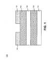
- FIG. 1illustrates the cross-section of a semiconductor device 100 formed in accordance with an embodiment of the present invention.
- semiconductor device 100may include a silicon on insulator (SOI) structure that includes a silicon substrate 110 , a buried oxide layer 120 and a silicon layer 130 on the buried oxide layer 120 . Buried oxide layer 120 and silicon layer 130 may be formed on substrate 110 in a conventional manner.
- SOIsilicon on insulator
- buried oxide layer 120may include a silicon oxide, such as SiO 2 , and may have a thickness ranging from about 1500 ⁇ to about 3000 ⁇ .
- Silicon layer 130may include monocrystalline or polycrystalline silicon having a thickness ranging from about 200 ⁇ to about 1000 ⁇ . Silicon layer 130 is used to form multiple active lines or fins for a double gate transistor device, as described in more detail below.
- substrate 110 and layer 130may comprise other semiconducting materials, such as germanium, or combinations of semiconducting materials, such as silicon-germanium.
- Buried oxide layer 120may also include other dielectric materials.
- a dielectric layer 140such as a silicon oxide layer, may be formed over silicon layer 130 to act as a protective mask during subsequent etching processes.
- dielectric layer 140may comprise SiO 2 and may be deposited using chemical vapor deposition (CVD) to a thickness ranging from about 300 ⁇ to about 1000 ⁇ .
- CVDchemical vapor deposition
- layer 140may consist of other films or materials that may be deposited or grown, including conductive materials or other non-conductive materials.
- a photoresist materialmay be deposited and patterned to form a photoresist mask 150 , as illustrated in FIG. 1 .
- the photoresistmay be deposited and patterned in any conventional manner.
- the dielectric layer 140 and photoresist mask 150may be used to facilitate the formation of a number of active lines, as described in more detail below.
- semiconductor device 100may then be etched.
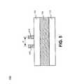
- dielectric layer 140may be etched to form trench 210 , as illustrated in FIG. 2 .
- the cross-sectional width of the trench 210is represented by L.
- Lmay range from about 1000 ⁇ to about 3000 ⁇ . It should be understood, however, that the particular value of L may vary based on the particular circuit requirements associated with the fins in the FinFET device that will be formed.
- the depth of trench 210 from the top surface of dielectric layer 140may range from, for example, about 300 ⁇ to about 1000 ⁇ .
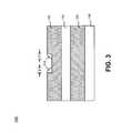
- trench spacers 310may be used as a hard mask to facilitate the formation of fins, as described in more detail below.
- the width of trench spacers 310is illustrated in FIG. 3 as “S.” In an exemplary implementation, S may range from about 100 ⁇ to about 500 ⁇ . However, the particular width of trench spacers 310 (and the value of S) may be set based on the desired pitch associated with the subsequently formed fins.
- dielectric layer 140may be etched, with the etching terminating on silicon layer 130 as illustrated in FIG. 4 .
- the trench spacers 310protect the material in dielectric layer 140 located below the trench spacers 310 from being etched, resulting in dielectric structures 410 .
- the trench spacers 310may be removed, as illustrated in FIG. 5 .
- the center-to-center distance between the dielectric structures 410referred to as the pitch
- Pthe center-to-center distance between the dielectric structures 410
- the particular value of P that may be obtained in accordance with the present inventionmay be very small, e.g., as small as about 500 ⁇ . However, as discussed above, it should be understood that the particular value of P may vary based on the particular circuit requirements associated with the fins and double gate device that will be formed.
- Silicon layer 130may then be etched, with the etching terminating on buried oxide layer 120 , as illustrated in FIG. 6 .
- dielectric structures 410act as a mask to protect the silicon material in silicon layer 130 located below the dielectric structures 410 from being etched, resulting in fin structures 610 illustrated in FIG. 6 .
- Dielectric structures 410may then be removed, for example, via a planarization process, resulting in fin structures 610 illustrated in FIG. 7 .
- Fin structures 610may be used as fins in a FinFET device or as active lines in other devices.
- the pitch P of the fins formed in accordance with the present inventionmay be very small.
- a protective dielectric layersuch as a silicon nitride or silicon oxide may be formed on the top surface of fins 610 , followed by the formation of a gate dielectric on the side surfaces of the fins 610 .
- Source/drain regionsmay then be formed at the respective ends of the fins 610 , followed by formation of one or more gates.
- a silicon layer, germanium layer, combinations of silicon and germanium or various metalsmay be used as the gate material.
- the gate materialmay then be patterned and etched to form the gate electrodes.
- FIG. 8illustrates a top view of semiconductor device 100 consistent with the present invention after the source/drain regions and gate electrodes are formed.
- semiconductor device 100includes a double gate structure with fins 610 , source drain regions 810 and 820 , and gate electrodes 830 and 840 .
- the source/drain regions 810 and 820may then be doped with n-type or p-type impurities based on the particular end device requirements.
- sidewall spacersmay optionally be formed prior to the source/drain ion implantation to control the location of the source/drain junctions based on the particular circuit requirements.
- Activation annealingmay then be performed to activate the source/drain regions 810 and 820 .
- the present inventionhas been described above as forming two fins.
- the methodology of the present inventionmay be used to form any number of fins, based on the particular circuit requirements. For example, if more than two fins are required, multiple trenches may be formed in dielectric layer 140 (FIG. 2 ). The processing for forming the fins may then proceed as described above with respect to FIGS. 3-7. In this case, the distance between neighboring trenches may be set to a predetermined distance so that the fin subsequently formed below one of the trenches is located the desired distance from another fin subsequently formed below a neighboring trench.
- a FinFET devicemay be formed with multiple fins having a small pitch.
- the methodology for forming fins in accordance with the present inventionallows multiple fins to be formed more closely together than that realized in conventional processing. Having multiple fins enables the resulting semiconductor device to increase the channel width per device as compared to a single fin FinFET device.
- the present inventionis able to provide more fins in a smaller area than that obtained using conventional processes. Therefore, the present invention provides increased flexibility and can be easily integrated into conventional processing.
- FIG. 9Aillustrates a cross-sectional view of semiconductor device 900 that includes gate 910 , source region 920 and drain region 930 .
- the semiconductor device 900may be a FinFET device.
- the fin(s) in device 900are not shown for simplicity.
- a tilt angle implant processmay be performed to dope the source and drain regions 920 / 930 as indicated by the arrows in FIG. 9 A.
- the source region 920 and drain region 930may be asymmetrical with respect to gate 910 , as illustrated in FIG. 9 B. That is, the source region 920 may extend laterally below gate 910 , while drain region 930 may not extend laterally below gate 910 , as illustrated in FIG. 9 B.
- the FinFET 900may include asymmetrical source/drain extension regions.
- FIG. 10illustrates the cross-section of semiconductor device 1000 that includes a buried oxide layer 1010 that may be formed on a substrate.
- a fin 1020comprising silicon, and a gate dielectric 1030 may be formed on the top surface and sidewalls of fin 1020 in a conventional manner, as illustrated in FIG. 10 .
- a polysilicon layer 1040may be deposited, as illustrated in FIG. 10 .
- Polysilicon layer 1040may then be doped with n-type or p-type impurities.
- a second polysilicon layer 1050may be deposited, as illustrated in FIG. 10 .
- Polysilicon layer 1050may then be doped with n-type or p-type impurities. Polysilicon layers 1040 and 1050 may then be patterned and etched to form one or more gates. The resulting semiconductor device 1000 experiences reduced poly resistance as compared to conventional devices.
- the dielectric and conductive layers used in manufacturing a semiconductor device in accordance with the present inventioncan be deposited by conventional deposition techniques.
- metallization techniquessuch as various types of CVD processes, including low pressure CVD (LPCVD) and enhanced CVD (ECVD) can be employed.
- LPCVDlow pressure CVD
- ECVDenhanced CVD
- the present inventionis applicable in the manufacturing of double-gate semiconductor devices and particularly in FinFET devices with design features of 100 nm and below.
- the present inventionis applicable to the formation of any of various types of semiconductor devices, and hence, details have not been set forth in order to avoid obscuring the thrust of the present invention.
- conventional photolithographic and etching techniquesare employed and, hence, the details of such techniques have not been set forth herein in detail.
Landscapes
- Thin Film Transistor (AREA)
- Insulated Gate Type Field-Effect Transistor (AREA)
Abstract
Description
Claims (19)
Priority Applications (1)
| Application Number | Priority Date | Filing Date | Title |
|---|---|---|---|
| US10/274,951US6706571B1 (en) | 2002-10-22 | 2002-10-22 | Method for forming multiple structures in a semiconductor device |
Applications Claiming Priority (1)
| Application Number | Priority Date | Filing Date | Title |
|---|---|---|---|
| US10/274,951US6706571B1 (en) | 2002-10-22 | 2002-10-22 | Method for forming multiple structures in a semiconductor device |
Publications (1)
| Publication Number | Publication Date |
|---|---|
| US6706571B1true US6706571B1 (en) | 2004-03-16 |
Family
ID=31946536
Family Applications (1)
| Application Number | Title | Priority Date | Filing Date |
|---|---|---|---|
| US10/274,951Expired - LifetimeUS6706571B1 (en) | 2002-10-22 | 2002-10-22 | Method for forming multiple structures in a semiconductor device |
Country Status (1)
| Country | Link |
|---|---|
| US (1) | US6706571B1 (en) |
Cited By (266)
| Publication number | Priority date | Publication date | Assignee | Title |
|---|---|---|---|---|
| US20040036126A1 (en)* | 2002-08-23 | 2004-02-26 | Chau Robert S. | Tri-gate devices and methods of fabrication |
| US20040180499A1 (en)* | 2003-03-12 | 2004-09-16 | Doyle Brian S. | Method of forming an element of a microelectronic circuit |
| US20040197975A1 (en)* | 2003-01-23 | 2004-10-07 | Zoran Krivokapic | Narrow fin finfet |
| US6812119B1 (en)* | 2003-07-08 | 2004-11-02 | Advanced Micro Devices, Inc. | Narrow fins by oxidation in double-gate finfet |
| US20040217433A1 (en)* | 2003-04-29 | 2004-11-04 | Yee-Chia Yeo | Doping of semiconductor fin devices |
| US20040222477A1 (en)* | 2003-05-05 | 2004-11-11 | International Business Machines Corporation | Multi-height finfets |
| US20040262676A1 (en)* | 2003-06-30 | 2004-12-30 | Deok-Hyung Lee | Methods of fabricating Fin-field effect transistors (Fin-FETs) having protection layers and devices related thereto |
| US20040266077A1 (en)* | 2003-06-27 | 2004-12-30 | Yee-Chia Yeo | Structure and method for forming the gate electrode in a multiple-gate transistor |
| GB2404283A (en)* | 2003-07-24 | 2005-01-26 | Samsung Electronics Co Ltd | Multi channel TFT |
| US20050056888A1 (en)* | 2003-09-16 | 2005-03-17 | Jae-Man Youn | Double gate field effect transistor and method of manufacturing the same |
| US6872647B1 (en)* | 2003-05-06 | 2005-03-29 | Advanced Micro Devices, Inc. | Method for forming multiple fins in a semiconductor device |
| US20050082578A1 (en)* | 2003-06-25 | 2005-04-21 | Nowak Edward J. | High-density FinFET integration scheme |
| US20050104091A1 (en)* | 2003-11-04 | 2005-05-19 | Tabery Cyrus E. | Self aligned damascene gate |
| US20050121706A1 (en)* | 2003-02-20 | 2005-06-09 | Hao-Yu Chen | Semiconductor nano-rod devices |
| US20050148137A1 (en)* | 2003-12-30 | 2005-07-07 | Brask Justin K. | Nonplanar transistors with metal gate electrodes |
| US20050158970A1 (en)* | 2004-01-16 | 2005-07-21 | Robert Chau | Tri-gate transistors and methods to fabricate same |
| US20050193143A1 (en)* | 2003-12-30 | 2005-09-01 | Meyers Brian R. | Framework for user interaction with multiple network devices |
| US20050218438A1 (en)* | 2004-03-31 | 2005-10-06 | Nick Lindert | Bulk non-planar transistor having strained enhanced mobility and methods of fabrication |
| US6960507B2 (en) | 2003-07-24 | 2005-11-01 | Samsung Electronics Co., Ltd. | Vertical double-channel silicon-on-insulator transistor and method of manufacturing the same |
| US20050242406A1 (en)* | 2003-06-27 | 2005-11-03 | Hareland Scott A | Nonplanar device with stress incorporation layer and method of fabrication |
| US20050266692A1 (en)* | 2004-06-01 | 2005-12-01 | Brask Justin K | Method of patterning a film |
| US20050275010A1 (en)* | 2004-06-10 | 2005-12-15 | Hung-Wei Chen | Semiconductor nano-wire devices and methods of fabrication |
| US20060033095A1 (en)* | 2004-08-10 | 2006-02-16 | Doyle Brian S | Non-planar pMOS structure with a strained channel region and an integrated strained CMOS flow |
| US20060046200A1 (en)* | 2004-09-01 | 2006-03-02 | Abatchev Mirzafer K | Mask material conversion |
| US20060046201A1 (en)* | 2004-09-02 | 2006-03-02 | Sandhu Gurtej S | Method to align mask patterns |
| US20060063332A1 (en)* | 2004-09-23 | 2006-03-23 | Brian Doyle | U-gate transistors and methods of fabrication |
| US20060068591A1 (en)* | 2004-09-29 | 2006-03-30 | Marko Radosavljevic | Fabrication of channel wraparound gate structure for field-effect transistor |
| US20060086977A1 (en)* | 2004-10-25 | 2006-04-27 | Uday Shah | Nonplanar device with thinned lower body portion and method of fabrication |
| US20060128131A1 (en)* | 2004-09-29 | 2006-06-15 | Chang Peter L | Independently accessed double-gate and tri-gate transistors in same process flow |
| US20060138553A1 (en)* | 2004-09-30 | 2006-06-29 | Brask Justin K | Nonplanar transistors with metal gate electrodes |
| US20060139496A1 (en)* | 2004-12-27 | 2006-06-29 | Sanyo Electric Co., Ltd. | Video signal processing apparatus |
| US20060157687A1 (en)* | 2005-01-18 | 2006-07-20 | Doyle Brian S | Non-planar MOS structure with a strained channel region |
| US20060172497A1 (en)* | 2003-06-27 | 2006-08-03 | Hareland Scott A | Nonplanar semiconductor device with partially or fully wrapped around gate electrode and methods of fabrication |
| US20060177977A1 (en)* | 2005-02-08 | 2006-08-10 | The Hong Kong University Of Science And Technology | Method for patterning fins and gates in a FinFET device using trimmed hard-mask capped with imaging layer |
| US20060186484A1 (en)* | 2005-02-23 | 2006-08-24 | Chau Robert S | Field effect transistor with narrow bandgap source and drain regions and method of fabrication |
| US20060194378A1 (en)* | 2004-11-05 | 2006-08-31 | Kabushiki Kaisha Toshiba | Semiconductor device and method of fabricating the same |
| US20060202266A1 (en)* | 2005-03-14 | 2006-09-14 | Marko Radosavljevic | Field effect transistor with metal source/drain regions |
| US20060211260A1 (en)* | 2005-03-15 | 2006-09-21 | Luan Tran | Pitch reduced patterns relative to photolithography features |
| US20060216922A1 (en)* | 2005-03-28 | 2006-09-28 | Tran Luan C | Integrated circuit fabrication |
| US20060223302A1 (en)* | 2005-03-31 | 2006-10-05 | Chang Peter L | Self-aligned contacts for transistors |
| US20060228854A1 (en)* | 2004-08-31 | 2006-10-12 | Luan Tran | Methods for increasing photo alignment margins |
| US20060246685A1 (en)* | 2005-04-28 | 2006-11-02 | Tomohiro Saito | Semiconductor device fabrication method |
| US20060258162A1 (en)* | 2004-09-02 | 2006-11-16 | Abatchev Mirzafer K | Method for integrated circuit fabrication using pitch multiplication |
| US20060263699A1 (en)* | 2005-05-23 | 2006-11-23 | Mirzafer Abatchev | Methods for forming arrays of a small, closely spaced features |
| US20060273456A1 (en)* | 2005-06-02 | 2006-12-07 | Micron Technology, Inc., A Corporation | Multiple spacer steps for pitch multiplication |
| US20060281266A1 (en)* | 2005-06-09 | 2006-12-14 | Wells David H | Method and apparatus for adjusting feature size and position |
| KR100657969B1 (en) | 2005-08-30 | 2006-12-14 | 삼성전자주식회사 | A manufacturing method of a semiconductor device having a single gate electrode corresponding to a pair of pin-type channel regions |
| US20060278911A1 (en)* | 2005-06-14 | 2006-12-14 | Eppich Anton P | Relaxed-pitch method of aligning active area to digit line |
| US20060286755A1 (en)* | 2005-06-15 | 2006-12-21 | Brask Justin K | Method for fabricating transistor with thinned channel |
| US20070001237A1 (en)* | 2005-07-01 | 2007-01-04 | Tsu-Jae King | Segmented channel MOS transistor |
| US20070001232A1 (en)* | 2005-07-01 | 2007-01-04 | Tsu-Jae King | Integrated circuit on corrugated substrate |
| US20070001173A1 (en)* | 2005-06-21 | 2007-01-04 | Brask Justin K | Semiconductor device structures and methods of forming semiconductor structures |
| US20070001219A1 (en)* | 2005-06-30 | 2007-01-04 | Marko Radosavljevic | Block contact architectures for nanoscale channel transistors |
| US20070018206A1 (en)* | 2005-07-06 | 2007-01-25 | Leonard Forbes | Surround gate access transistors with grown ultra-thin bodies |
| US20070026672A1 (en)* | 2005-07-29 | 2007-02-01 | Micron Technology, Inc. | Pitch doubled circuit layout |
| US20070029624A1 (en)* | 2005-08-03 | 2007-02-08 | International Business Machines Corporation | Fin-type field effect transistor |
| US20070049011A1 (en)* | 2005-09-01 | 2007-03-01 | Micron Technology, Inc., A Corporation | Method of forming isolated features using pitch multiplication |
| US20070048674A1 (en)* | 2005-09-01 | 2007-03-01 | Wells David H | Methods for forming arrays of small, closely spaced features |
| US20070049030A1 (en)* | 2005-09-01 | 2007-03-01 | Sandhu Gurtej S | Pitch multiplication spacers and methods of forming the same |
| US20070050748A1 (en)* | 2005-08-30 | 2007-03-01 | Micron Technology, Inc., A Corporation | Method and algorithm for random half pitched interconnect layout with constant spacing |
| US20070049032A1 (en)* | 2005-09-01 | 2007-03-01 | Mirzafer Abatchev | Protective coating for planarization |
| US20070049040A1 (en)* | 2005-03-15 | 2007-03-01 | Micron Technology, Inc., A Corporation | Multiple deposition for integration of spacers in pitch multiplication process |
| US20070045712A1 (en)* | 2005-09-01 | 2007-03-01 | Haller Gordon A | Memory cell layout and process flow |
| US20070051997A1 (en)* | 2005-08-31 | 2007-03-08 | Gordon Haller | Semiconductor memory device |
| EP1764827A1 (en)* | 2005-09-16 | 2007-03-21 | Interuniversitair Microelektronica Centrum ( Imec) | Recursive spacer defined patterning |
| US20070063276A1 (en)* | 2005-09-19 | 2007-03-22 | International Business Machines Corporation | DENSE CHEVRON finFET AND METHOD OF MANUFACTURING SAME |
| US20070090363A1 (en)* | 2005-07-25 | 2007-04-26 | Abbott Todd R | Dram including a vertical surround gate transistor |
| US20070090416A1 (en)* | 2005-09-28 | 2007-04-26 | Doyle Brian S | CMOS devices with a single work function gate electrode and method of fabrication |
| US20070090408A1 (en)* | 2005-09-29 | 2007-04-26 | Amlan Majumdar | Narrow-body multiple-gate FET with dominant body transistor for high performance |
| US20070105357A1 (en)* | 2005-09-01 | 2007-05-10 | Micron Technology, Inc. | Silicided recessed silicon |
| US20070140637A1 (en)* | 2005-05-27 | 2007-06-21 | Staf Verhaegen | Method for high topography patterning |
| US20070148837A1 (en)* | 2005-12-27 | 2007-06-28 | Uday Shah | Method of fabricating a multi-cornered film |
| US20070159617A1 (en)* | 2006-01-11 | 2007-07-12 | Mackey Jeffrey L | Photolithographic systems and methods for producing sub-diffraction-limited features |
| US7265008B2 (en) | 2005-07-01 | 2007-09-04 | Synopsys, Inc. | Method of IC production using corrugated substrate |
| US20070205438A1 (en)* | 2006-03-02 | 2007-09-06 | Werner Juengling | Masking process for simultaneously patterning separate regions |
| US20070205443A1 (en)* | 2006-03-02 | 2007-09-06 | Werner Juengling | Vertical gated access transistor |
| US20070228372A1 (en)* | 2004-10-19 | 2007-10-04 | Taiwan Semiconductor Manufacturing Company, Ltd. | Method for Fabricating a Body Contact in a Finfet Structure and a Device Including the Same |
| US20070238308A1 (en)* | 2006-04-07 | 2007-10-11 | Ardavan Niroomand | Simplified pitch doubling process flow |
| US20070238273A1 (en)* | 2006-03-31 | 2007-10-11 | Doyle Brian S | Method of ion implanting for tri-gate devices |
| US20070249170A1 (en)* | 2006-04-25 | 2007-10-25 | David Kewley | Process for improving critical dimension uniformity of integrated circuit arrays |
| US20070261016A1 (en)* | 2006-04-24 | 2007-11-08 | Sandhu Gurtej S | Masking techniques and templates for dense semiconductor fabrication |
| US20070290250A1 (en)* | 2004-03-18 | 2007-12-20 | Clark William F Jr | Multiple dielectric finfet structure and method |
| US20080006908A1 (en)* | 2006-07-10 | 2008-01-10 | Taiwan Semiconductor Manufacturing Company, Ltd. | Body-tied, strained-channel multi-gate device and methods of manufacturing same |
| US20080057692A1 (en)* | 2006-08-30 | 2008-03-06 | Wells David H | Single spacer process for multiplying pitch by a factor greater than two and related intermediate IC structures |
| US20080070165A1 (en)* | 2006-09-14 | 2008-03-20 | Mark Fischer | Efficient pitch multiplication process |
| US20080079077A1 (en)* | 2004-06-04 | 2008-04-03 | Nec Corporation | Semiconductor Device And Manufacturing Method Thereof |
| US20080085612A1 (en)* | 2006-10-05 | 2008-04-10 | Micron Technology, Inc. | Method to deposit conformal low temperature SiO2 |
| US20080149593A1 (en)* | 2005-08-25 | 2008-06-26 | Micron Technology, Inc. | Multiple deposition for integration of spacers in pitch multiplication process |
| US20080157225A1 (en)* | 2006-12-29 | 2008-07-03 | Suman Datta | SRAM and logic transistors with variable height multi-gate transistor architecture |
| US20080157182A1 (en)* | 2006-12-27 | 2008-07-03 | Samsung Electronics Co., Ltd. | Semiconductor device and method of fabricating the same |
| US7402875B2 (en) | 2005-08-17 | 2008-07-22 | Intel Corporation | Lateral undercut of metal gate in SOI device |
| US20080179682A1 (en)* | 2007-01-31 | 2008-07-31 | Infineon Technologies Ag | Circuit layout for different performance and method |
| US20080185650A1 (en)* | 2007-02-01 | 2008-08-07 | Taiwan Semiconductor Manufacturing Co., Ltd. | FinFET for device characterization |
| US20080277745A1 (en)* | 2007-05-07 | 2008-11-13 | Taiwan Semiconductor Manufacturing Co., Ltd. | Fin filled effect transistor and method of forming the same |
| US20080299753A1 (en)* | 2005-09-01 | 2008-12-04 | Figura Thomas A | Peripheral Gate Stacks and Recessed Array Gates |
| US20080296691A1 (en)* | 2007-05-30 | 2008-12-04 | Harry Chuang | Layout methods of integrated circuits having unit MOS devices |
| US20080299774A1 (en)* | 2007-06-04 | 2008-12-04 | Micron Technology, Inc. | Pitch multiplication using self-assembling materials |
| US20090014798A1 (en)* | 2007-07-11 | 2009-01-15 | International Business Machines Corporation | Finfet sram with asymmetric gate and method of manufacture thereof |
| US7479421B2 (en) | 2005-09-28 | 2009-01-20 | Intel Corporation | Process for integrating planar and non-planar CMOS transistors on a bulk substrate and article made thereby |
| US20090035665A1 (en)* | 2007-07-31 | 2009-02-05 | Micron Technology, Inc. | Process of semiconductor fabrication with mask overlay on pitch multiplied features and associated structures |
| US20090035909A1 (en)* | 2007-07-31 | 2009-02-05 | Taiwan Semiconductor Manufacturing Company, Ltd. | Method of fabrication of a finfet element |
| US20090096002A1 (en)* | 2007-10-15 | 2009-04-16 | Chen-Hua Yu | System and Method for Source/Drain Contact Processing |
| US20090095980A1 (en)* | 2007-10-16 | 2009-04-16 | Chen-Hua Yu | Reducing Resistance in Source and Drain Regions of FinFETs |
| US20090127722A1 (en)* | 2007-11-20 | 2009-05-21 | Christoph Noelscher | Method for Processing a Spacer Structure, Method of Manufacturing an Integrated Circuit, Semiconductor Device and Intermediate Structure with at Least One Spacer Structure |
| US20090152645A1 (en)* | 2007-12-18 | 2009-06-18 | Micron Technology, Inc. | Methods for isolating portions of a loop of pitch-multiplied material and related structures |
| US20090253266A1 (en)* | 2007-04-27 | 2009-10-08 | Chen-Hua Yu | Semiconductor Device Having Multiple Fin Heights |
| US20090278196A1 (en)* | 2008-05-06 | 2009-11-12 | Cheng-Hung Chang | FinFETs having dielectric punch-through stoppers |
| US20100006945A1 (en)* | 2008-06-11 | 2010-01-14 | Taiwan Semiconductor Manufacturing Company, Ltd. | Finfet drive strength modification |
| US7659208B2 (en) | 2007-12-06 | 2010-02-09 | Micron Technology, Inc | Method for forming high density patterns |
| US20100052059A1 (en)* | 2008-08-28 | 2010-03-04 | Taiwan Semiconductor Manufacturing Company, Ltd. | Finfet process compatible native transistor |
| US20100062579A1 (en)* | 2008-09-11 | 2010-03-11 | Micron Technology, Inc. | Self-aligned trench formation |
| US20100065888A1 (en)* | 2004-06-30 | 2010-03-18 | Shaheen Mohamad A | High mobility tri-gate devices and methods of fabrication |
| US20100072553A1 (en)* | 2008-09-23 | 2010-03-25 | Taiwan Semiconductor Manufacturing Co., Ltd. | METAL GATE STRESS FILM FOR MOBILITY ENHANCEMENT IN FinFET DEVICE |
| US20100130016A1 (en)* | 2008-11-24 | 2010-05-27 | Micron Technology, Inc. | Methods of forming a masking pattern for integrated circuits |
| US20100136791A1 (en)* | 2008-12-01 | 2010-06-03 | Chih-Yu Lai | Method of Reducing Delamination in the Fabrication of Small-Pitch Devices |
| US20100144121A1 (en)* | 2008-12-05 | 2010-06-10 | Cheng-Hung Chang | Germanium FinFETs Having Dielectric Punch-Through Stoppers |
| US7737039B2 (en) | 2007-11-01 | 2010-06-15 | Micron Technology, Inc. | Spacer process for on pitch contacts and related structures |
| US20100167506A1 (en)* | 2008-12-31 | 2010-07-01 | Taiwan Semiconductor Manufacturing Co., Ltd. | Inductive plasma doping |
| US20100163842A1 (en)* | 2008-12-29 | 2010-07-01 | Li-Shyue Lai | Multiple-Gate Transistors with Reverse T-Shaped Fins |
| US20100165707A1 (en)* | 2008-12-29 | 2010-07-01 | Yen-Huei Chen | Read/Write Margin Improvement in SRAM Design Using Dual-Gate Transistors |
| US20100167520A1 (en)* | 2008-12-31 | 2010-07-01 | Sandisk 3D Llc | Resist feature and removable spacer pitch doubling patterning method for pillar structures |
| US20100163971A1 (en)* | 2008-12-31 | 2010-07-01 | Shih-Ting Hung | Dielectric Punch-Through Stoppers for Forming FinFETs Having Dual Fin Heights |
| US20100183961A1 (en)* | 2009-01-20 | 2010-07-22 | Taiwan Semiconductor Manufacturing Company, Ltd. | Integrated circuit layout design |
| US20100190345A1 (en)* | 2009-01-26 | 2010-07-29 | Neng-Kuo Chen | Selective Etch-Back Process for Semiconductor Devices |
| US20100187656A1 (en)* | 2009-01-28 | 2010-07-29 | Po-Yao Ke | Bipolar Junction Transistors and Methods of Fabrication Thereof |
| US20100193916A1 (en)* | 2008-12-31 | 2010-08-05 | Sandisk 3D Llc | Methods for increased array feature density |
| US20100202184A1 (en)* | 2009-02-10 | 2010-08-12 | Jam-Wem Lee | One-Time Programmable Fuse with Ultra Low Programming Current |
| US20100203734A1 (en)* | 2009-02-12 | 2010-08-12 | Taiwan Semiconductor Manufacturing Company, Ltd. | Method of pitch halving |
| US20100214863A1 (en)* | 2009-02-23 | 2010-08-26 | Taiwan Semiconductor Manufacturing Company, Ltd. | Memory power gating circuit and methods |
| US20100213548A1 (en)* | 2009-02-24 | 2010-08-26 | Cheng-Hung Chang | Semiconductor Devices with Low Junction Capacitances and Methods of Fabrication Thereof |
| US7795149B2 (en) | 2006-06-01 | 2010-09-14 | Micron Technology, Inc. | Masking techniques and contact imprint reticles for dense semiconductor fabrication |
| US20100232203A1 (en)* | 2009-03-16 | 2010-09-16 | Taiwan Semiconductor Manufacturing Company, Ltd. | Electrical anti-fuse and related applications |
| US20100230757A1 (en)* | 2009-03-16 | 2010-09-16 | Taiwan Semiconductor Manufacturing Company, Ltd. | Hybrid STI Gap-Filling Approach |
| US20100237419A1 (en)* | 2009-03-20 | 2010-09-23 | Lie-Yong Yang | Static Random Access Memory (SRAM) Cell and Method for Forming Same |
| US20100244144A1 (en)* | 2009-03-31 | 2010-09-30 | Taiwan Semiconductor Manufacturing Company, Ltd. | Electrical fuse and related applications |
| US20100252862A1 (en)* | 2009-04-01 | 2010-10-07 | Chih-Hsin Ko | Source/Drain Engineering of Devices with High-Mobility Channels |
| US20100252816A1 (en)* | 2009-04-01 | 2010-10-07 | Taiwan Semiconductor Manufacturing Company, Ltd. | High-Mobility Multiple-Gate Transistor with Improved On-to-Off Current Ratio |
| US20100258870A1 (en)* | 2009-04-14 | 2010-10-14 | Taiwan Semiconductor Manufacturing Company, Ltd. | Finfets and methods for forming the same |
| US20100264468A1 (en)* | 2009-04-17 | 2010-10-21 | Taiwan Semiconductor Manufacturing Company, Ltd. | Method Of Fabrication Of A FinFET Element |
| US20100267172A1 (en)* | 2009-04-20 | 2010-10-21 | Taiwan Semiconductor Manufacturing Co., Ltd. | Formation of Shallow Trench Isolation Using Chemical Vapor Etch |
| US20100276761A1 (en)* | 2009-04-29 | 2010-11-04 | Taiwan Semiconductor Manufacturing Company, Ltd. | Non-Planar Transistors and Methods of Fabrication Thereof |
| US20100276668A1 (en)* | 2009-04-30 | 2010-11-04 | Chih-Hsin Ko | Reducing Source/Drain Resistance of III-V Based Transistors |
| US7829262B2 (en) | 2005-08-31 | 2010-11-09 | Micron Technology, Inc. | Method of forming pitch multipled contacts |
| US20100292963A1 (en)* | 2009-04-15 | 2010-11-18 | James Schroeder | Personal fit medical implants and orthopedic surgical instruments and methods for making |
| US20100296213A1 (en)* | 2009-02-19 | 2010-11-25 | Jam-Wem Lee | ESD Protection for FinFETs |
| US20100301390A1 (en)* | 2009-05-29 | 2010-12-02 | Chih-Hsin Ko | Gradient Ternary or Quaternary Multiple-Gate Transistor |
| US20100301392A1 (en)* | 2009-06-01 | 2010-12-02 | Chih-Hsin Ko | Source/Drain Re-Growth for Manufacturing III-V Based Transistors |
| US20100317181A1 (en)* | 2009-06-12 | 2010-12-16 | Taiwan Semiconductor Manufacturing Company, Ltd. | Gate Stack Integration of Complementary MOS Devices |
| US20100320572A1 (en)* | 2009-06-22 | 2010-12-23 | Taiwan Semiconductor Manufacturing Co., Ltd. | Thin-Body Bipolar Device |
| US20100330806A1 (en)* | 2009-06-29 | 2010-12-30 | Sandisk 3D Llc | Method of forming contact hole arrays using a hybrid spacer technique |
| US20110006390A1 (en)* | 2009-07-08 | 2011-01-13 | Taiwan Semiconductor Manufacturing Company, Ltd. | Sti structure and method of forming bottom void in same |
| US20110024804A1 (en)* | 2009-07-28 | 2011-02-03 | Taiwan Semiconductor Manufacturing Company, Ltd. | Method for forming high germanium concentration sige stressor |
| US20110024794A1 (en)* | 2009-07-31 | 2011-02-03 | Taiwan Semiconductor Manufacturing Company, Ltd. | Fin structure for high mobility multiple-gate transistor |
| US20110049613A1 (en)* | 2009-09-01 | 2011-03-03 | Taiwan Semiconductor Manufacturing Company, Ltd. | Accumulation type finfet, circuits and fabrication method thereof |
| US20110068405A1 (en)* | 2009-09-24 | 2011-03-24 | Taiwan Semiconductor Manufacturing Company, Ltd. | Fin field effect transistor |
| US20110068407A1 (en)* | 2009-09-24 | 2011-03-24 | Taiwan Semiconductor Manufacturing Company, Ltd. | Germanium FinFETs with Metal Gates and Stressors |
| US20110073952A1 (en)* | 2009-09-29 | 2011-03-31 | Taiwan Semiconductor Manufacturing Company, Ltd. | Controlling the Shape of Source/Drain Regions in FinFETs |
| US20110073919A1 (en)* | 2009-09-29 | 2011-03-31 | Taiwan Semiconductor Manufacturing Company, Ltd. | Method of fabricating finfet device |
| US20110079829A1 (en)* | 2009-10-01 | 2011-04-07 | Taiwan Semiconductor Manufacturing Company, Ltd. | Finfets and methods for forming the same |
| US20110084340A1 (en)* | 2009-10-14 | 2011-04-14 | Feng Yuan | Voids in STI Regions for Forming Bulk FinFETs |
| US20110089526A1 (en)* | 2009-10-16 | 2011-04-21 | Taiwan Semiconductor Manufacturing Company, Ltd. | Integrated Circuit with Multi Recessed Shallow Trench Isolation |
| US20110095378A1 (en)* | 2009-10-27 | 2011-04-28 | Taiwan Semiconductor Manufacturing Company, Ltd | FinFET Design with Reduced Current Crowding |
| US20110097867A1 (en)* | 2009-10-22 | 2011-04-28 | Taiwan Semiconductor Manufacturing Company, Ltd. | Method of controlling gate thicknesses in forming fusi gates |
| US20110097889A1 (en)* | 2009-10-27 | 2011-04-28 | Taiwan Semiconductor Manufacturing Company, Ltd. | STI Shape Near Fin Bottom of Si Fin in Bulk FinFET |
| US20110095372A1 (en)* | 2009-10-28 | 2011-04-28 | Taiwan Semiconductor Manufacturing Company, Ltd. | Forming Inter-Device STI Regions and Intra-Device STI Regions Using Different Dielectric Materials |
| US20110097863A1 (en)* | 2009-10-27 | 2011-04-28 | Taiwan Semiconductor Manufacturing Company, Ltd. | Cross OD FinFET Patterning |
| US20110101421A1 (en)* | 2009-10-30 | 2011-05-05 | Taiwan Semiconductor Manufacturing Company, Ltd. | Method of forming epi film in substrate trench |
| US20110117679A1 (en)* | 2009-11-19 | 2011-05-19 | Taiwan Semiconductor Manufacturing Company, Ltd. | Sacrificial offset protection film for a finfet device |
| US20110115024A1 (en)* | 2009-11-18 | 2011-05-19 | Taiwan Semiconductor Manufacturing Company, Ltd. | Non-Uniform Semiconductor Device Active Area Pattern Formation |
| US20110121383A1 (en)* | 2005-05-13 | 2011-05-26 | Micron Technology, Inc. | Memory array with surrounding gate access transistors and capacitors with global and staggered local bit lines |
| US20110121406A1 (en)* | 2009-11-20 | 2011-05-26 | Taiwan Semiconductor Manufacturing Company, Ltd. | FinFETs with Different Fin Heights |
| US20110127610A1 (en)* | 2009-12-02 | 2011-06-02 | Taiwan Semiconductor Manufacturing Company, Ltd. | Multiple-Gate Semiconductor Device and Method |
| US20110133285A1 (en)* | 2009-12-07 | 2011-06-09 | Taiwan Semiconductor Manufacturing Company, Ltd. | SRAM Structure with FinFETs Having Multiple Fins |
| US20110133292A1 (en)* | 2009-12-03 | 2011-06-09 | Taiwan Semiconductor Manufacturing Company, Ltd. | FinFETs with Multiple Fin Heights |
| US20110143510A1 (en)* | 2009-12-15 | 2011-06-16 | Taiwan Semiconductor Manufacturing Company, Ltd. | Method of controlling gate thickness in forming finfet devices |
| US20110147846A1 (en)* | 2009-12-22 | 2011-06-23 | Taiwan Semiconductor Manufacturing Company, Ltd | Method for incorporating impurity element in epi silicon process |
| US20110156148A1 (en)* | 2009-12-30 | 2011-06-30 | Taiwan Semiconductor Manufacturing Co., Ltd. | Semiconductor device and method for making the same using semiconductor fin density design rules |
| US20110165744A1 (en)* | 2005-05-13 | 2011-07-07 | Micron Technology | Memory array with ultra-thin etched pillar surround gate access transistors and buried data/bit lines |
| US20110171795A1 (en)* | 2010-01-12 | 2011-07-14 | Taiwan Semiconductor Manufacturing Company, Ltd. | FinFET LDD and Source Drain Implant Technique |
| US20110175165A1 (en)* | 2010-01-19 | 2011-07-21 | Taiwan Semiconductor Manufacturing Co., Ltd. | Semiconductor fin device and method for forming the same using high tilt angle implant |
| US20110182098A1 (en)* | 2010-01-27 | 2011-07-28 | Taiwan Semiconductor Manufacturing Company, Ltd. | Integrated circuits and methods for forming the same |
| US20110183508A1 (en)* | 2010-01-26 | 2011-07-28 | Taiwan Semiconductor Manufacturing Co., Ltd. | REPLACEMENT GATE FinFET DEVICES AND METHODS FOR FORMING THE SAME |
| US7989280B2 (en) | 2005-11-30 | 2011-08-02 | Intel Corporation | Dielectric interface for group III-V semiconductor device |
| US20110193141A1 (en)* | 2010-02-11 | 2011-08-11 | Taiwan Semiconductor Manufacturing Company, Ltd. | Method of fabricating a finfet device |
| US20110193175A1 (en)* | 2010-02-09 | 2011-08-11 | Taiwan Semiconductor Manufacturing Co., Ltd. | Lower parasitic capacitance finfet |
| US20110193178A1 (en)* | 2010-02-09 | 2011-08-11 | Taiwan Semiconductor Manufacturing Company, Ltd. | Bottom-Notched SiGe FinFET Formation Using Condensation |
| US20110195555A1 (en)* | 2010-02-09 | 2011-08-11 | Taiwan Semiconductor Manufacturing Company, Ltd. | Techniques for FinFET Doping |
| US20110195564A1 (en)* | 2010-02-08 | 2011-08-11 | Taiwan Semiconductor Manufacturing Company, Ltd. | Memory Cell Layout |
| US20110207279A1 (en)* | 2010-02-25 | 2011-08-25 | Taiwan Semiconductor Manufacturing Co., Ltd. | Integrated method for forming high-k metal gate finfet devices |
| US20110210404A1 (en)* | 2010-02-26 | 2011-09-01 | Taiwan Seminconductor Manufacturing Company, Ltd. | Epitaxy Profile Engineering for FinFETs |
| US20110223736A1 (en)* | 2010-03-09 | 2011-09-15 | Taiwan Semiconductor Manufacturing Company, Ltd. | LDD Epitaxy for FinFETs |
| US20110227162A1 (en)* | 2010-03-17 | 2011-09-22 | Taiwan Semiconductor Manufacturing Co., Ltd. | Method of making a finfet, and finfet formed by the method |
| US20110233679A1 (en)* | 2010-03-25 | 2011-09-29 | Taiwan Semiconductor Manufacturing Company, Ltd. | Integrated circuit including finfets and methods for forming the same |
| US8030218B2 (en) | 2008-03-21 | 2011-10-04 | Micron Technology, Inc. | Method for selectively modifying spacing between pitch multiplied structures |
| US8062963B1 (en) | 2010-10-08 | 2011-11-22 | Taiwan Semiconductor Manufacturing Company, Ltd. | Method of fabricating a semiconductor device having an epitaxy region |
| US8076208B2 (en) | 2008-07-03 | 2011-12-13 | Micron Technology, Inc. | Method for forming transistor with high breakdown voltage using pitch multiplication technique |
| US8080443B2 (en) | 2008-10-27 | 2011-12-20 | Sandisk 3D Llc | Method of making pillars using photoresist spacer mask |
| CN102299057A (en)* | 2010-06-28 | 2011-12-28 | 中芯国际集成电路制造(上海)有限公司 | Method for manufacturing fine patterns on semiconductor device |
| CN102339734A (en)* | 2010-07-15 | 2012-02-01 | 中芯国际集成电路制造(上海)有限公司 | Production method of cylindrical semiconductor device with cross section being circular ring |
| US8114573B2 (en) | 2006-06-02 | 2012-02-14 | Micron Technology, Inc. | Topography based patterning |
| CN102376542A (en)* | 2010-08-12 | 2012-03-14 | 中芯国际集成电路制造(上海)有限公司 | Production method of fine pattern of semiconductor |
| US8174073B2 (en) | 2007-05-30 | 2012-05-08 | Taiwan Semiconductor Manufacturing Co., Ltd. | Integrated circuit structures with multiple FinFETs |
| CN102446712A (en)* | 2011-09-08 | 2012-05-09 | 上海华力微电子有限公司 | Method for increasing double patterning process windows |
| US8187928B2 (en) | 2010-09-21 | 2012-05-29 | Taiwan Semiconductor Manufacturing Company, Ltd. | Methods of forming integrated circuits |
| US8212295B2 (en) | 2010-06-30 | 2012-07-03 | Taiwan Semiconductor Manufacturing Company, Ltd. | ROM cell circuit for FinFET devices |
| US8258848B2 (en) | 2010-09-07 | 2012-09-04 | Taiwan Semiconductor Manufacturing Co., Ltd. | Level shifter |
| US8278173B2 (en) | 2010-06-30 | 2012-10-02 | Taiwan Semiconductor Manufacturing Company, Ltd. | Method of fabricating gate structures |
| US8278196B2 (en) | 2010-07-21 | 2012-10-02 | Taiwan Semiconductor Manufacturing Company, Ltd. | High surface dopant concentration semiconductor device and method of fabricating |
| US8286114B2 (en) | 2007-04-18 | 2012-10-09 | Taiwan Semiconductor Manufacturing Company, Ltd. | 3-dimensional device design layout |
| US8298925B2 (en) | 2010-11-08 | 2012-10-30 | Taiwan Semiconductor Manufacturing Company, Ltd. | Mechanisms for forming ultra shallow junction |
| US8338305B2 (en) | 2010-10-19 | 2012-12-25 | Taiwan Semiconductor Manufacturing Company, Ltd. | Multi-fin device by self-aligned castle fin formation |
| US8362566B2 (en) | 2008-06-23 | 2013-01-29 | Intel Corporation | Stress in trigate devices using complimentary gate fill materials |
| US8367498B2 (en) | 2010-10-18 | 2013-02-05 | Taiwan Semiconductor Manufacturing Company, Ltd. | Fin-like field effect transistor (FinFET) device and method of manufacturing same |
| US8373229B2 (en) | 2010-08-30 | 2013-02-12 | Taiwan Semiconductor Manufacturing Company, Ltd. | Gate controlled bipolar junction transistor on fin-like field effect transistor (FinFET) structure |
| US8399931B2 (en) | 2010-06-30 | 2013-03-19 | Taiwan Semiconductor Manufacturing Company, Ltd. | Layout for multiple-fin SRAM cell |
| WO2013040845A1 (en)* | 2011-09-20 | 2013-03-28 | 中国科学院微电子研究所 | Semiconductor structure and method for manufacturing same |
| US8431453B2 (en) | 2011-03-31 | 2013-04-30 | Taiwan Semiconductor Manufacturing Company, Ltd. | Plasma doping to reduce dielectric loss during removal of dummy layers in a gate structure |
| CN103094112A (en)* | 2011-10-31 | 2013-05-08 | 中芯国际集成电路制造(上海)有限公司 | Formation method of fin parts of fin type transistor |
| US8440517B2 (en) | 2010-10-13 | 2013-05-14 | Taiwan Semiconductor Manufacturing Company, Ltd. | FinFET and method of fabricating the same |
| US8455929B2 (en) | 2010-06-30 | 2013-06-04 | Taiwan Semiconductor Manufacturing Company, Ltd. | Formation of III-V based devices on semiconductor substrates |
| US8482952B2 (en) | 2011-02-17 | 2013-07-09 | Taiwan Semiconductor Manufacturing Company, Ltd. | One time programming bit cell |
| US8486769B2 (en) | 2010-11-19 | 2013-07-16 | Taiwan Semiconductor Manufacturing Company, Ltd. | Method for forming metrology structures from fins in integrated circuitry |
| US8497528B2 (en) | 2010-05-06 | 2013-07-30 | Taiwan Semiconductor Manufacturing Company, Ltd. | Method for fabricating a strained structure |
| US20130207079A1 (en)* | 2012-02-09 | 2013-08-15 | International Business Machines Corporation | Tapered Nanowire Structure With Reduced Off Current |
| US8525267B2 (en) | 2010-11-23 | 2013-09-03 | Taiwan Semiconductor Manufacturing Company, Ltd. | Device and method for forming Fins in integrated circuitry |
| US8546242B2 (en) | 2008-02-18 | 2013-10-01 | Taiwan Semiconductor Manufacturing Company, Ltd. | Hybrid gap-fill approach for STI formation |
| US8592915B2 (en) | 2011-01-25 | 2013-11-26 | Taiwan Semiconductor Manufacturing Company, Ltd. | Doped oxide for shallow trench isolation (STI) |
| US8603924B2 (en) | 2010-10-19 | 2013-12-10 | Taiwan Semiconductor Manufacturing Company, Ltd. | Methods of forming gate dielectric material |
| US8609495B2 (en) | 2010-04-08 | 2013-12-17 | Taiwan Semiconductor Manufacturing Company, Ltd. | Hybrid gate process for fabricating finfet device |
| US8621398B2 (en) | 2010-05-14 | 2013-12-31 | Taiwan Semiconductor Manufacturing Company, Ltd. | Automatic layout conversion for FinFET device |
| US8617945B2 (en) | 2006-08-02 | 2013-12-31 | Intel Corporation | Stacking fault and twin blocking barrier for integrating III-V on Si |
| US8633076B2 (en) | 2010-11-23 | 2014-01-21 | Taiwan Semiconductor Manufacturing Company, Ltd. | Method for adjusting fin width in integrated circuitry |
| US8659072B2 (en) | 2010-09-24 | 2014-02-25 | Taiwan Semiconductor Manufacturing Company, Ltd. | Series FinFET implementation schemes |
| US8675397B2 (en) | 2010-06-25 | 2014-03-18 | Taiwan Semiconductor Manufacturing Company, Ltd. | Cell structure for dual-port SRAM |
| US8729627B2 (en) | 2010-05-14 | 2014-05-20 | Taiwan Semiconductor Manufacturing Company, Ltd. | Strained channel integrated circuit devices |
| US8759943B2 (en) | 2010-10-08 | 2014-06-24 | Taiwan Semiconductor Manufacturing Company, Ltd. | Transistor having notched fin structure and method of making the same |
| US8769446B2 (en) | 2010-11-12 | 2014-07-01 | Taiwan Semiconductor Manufacturing Company, Ltd. | Method and device for increasing fin device density for unaligned fins |
| US8796124B2 (en) | 2011-10-25 | 2014-08-05 | Taiwan Semiconductor Manufacturing Company, Ltd. | Doping method in 3D semiconductor device |
| US8796759B2 (en) | 2010-07-15 | 2014-08-05 | Taiwan Semiconductor Manufacturing Company, Ltd. | Fin-like field effect transistor (FinFET) device and method of manufacturing same |
| USRE45165E1 (en) | 2005-07-29 | 2014-09-30 | Taiwan Semiconductor Manufacturing Company, Ltd. | Structure for a multiple-gate FET device and a method for its fabrication |
| US8847324B2 (en) | 2012-12-17 | 2014-09-30 | Synopsys, Inc. | Increasing ION /IOFF ratio in FinFETs and nano-wires |
| US8877602B2 (en) | 2011-01-25 | 2014-11-04 | Taiwan Semiconductor Manufacturing Company, Ltd. | Mechanisms of doping oxide for forming shallow trench isolation |
| US8881084B2 (en) | 2010-05-14 | 2014-11-04 | Taiwan Semiconductor Manufacturing Company, Ltd. | FinFET boundary optimization |
| US8937353B2 (en) | 2010-03-01 | 2015-01-20 | Taiwan Semiconductor Manufacturing Co., Ltd. | Dual epitaxial process for a finFET device |
| US8942030B2 (en) | 2010-06-25 | 2015-01-27 | Taiwan Semiconductor Manufacturing Company, Ltd. | Structure and method for SRAM cell circuit |
| US8980719B2 (en) | 2010-04-28 | 2015-03-17 | Taiwan Semiconductor Manufacturing Company, Ltd. | Methods for doping fin field-effect transistors |
| US9029263B1 (en)* | 2013-12-12 | 2015-05-12 | Texas Instruments Incorporated | Method of printing multiple structure widths using spacer double patterning |
| US9040393B2 (en) | 2010-01-14 | 2015-05-26 | Taiwan Semiconductor Manufacturing Company, Ltd. | Method of forming semiconductor structure |
| US9048181B2 (en) | 2010-11-08 | 2015-06-02 | Taiwan Semiconductor Manufacturing Company, Ltd. | Mechanisms for forming ultra shallow junction |
| US9087725B2 (en) | 2009-12-03 | 2015-07-21 | Taiwan Semiconductor Manufacturing Company, Ltd. | FinFETs with different fin height and EPI height setting |
| US9112052B2 (en) | 2009-10-14 | 2015-08-18 | Taiwan Semiconductor Manufacturing Company, Ltd. | Voids in STI regions for forming bulk FinFETs |
| US9130058B2 (en) | 2010-07-26 | 2015-09-08 | Taiwan Semiconductor Manufacturing Company, Ltd. | Forming crown active regions for FinFETs |
| US9166022B2 (en) | 2010-10-18 | 2015-10-20 | Taiwan Semiconductor Manufacturing Company, Ltd. | Fin-like field effect transistor (FinFET) device and method of manufacturing same |
| US9177894B2 (en) | 2012-08-31 | 2015-11-03 | Synopsys, Inc. | Latch-up suppression and substrate noise coupling reduction through a substrate back-tie for 3D integrated circuits |
| US20160035571A1 (en)* | 2013-12-04 | 2016-02-04 | Taiwan Semiconductor Manufacturing Company, Ltd. | Lithography Using High Selectivity Spacers for Pitch Reduction |
| US9312064B1 (en) | 2015-03-02 | 2016-04-12 | Western Digital (Fremont), Llc | Method to fabricate a magnetic head including ion milling of read gap using dual layer hard mask |
| US9379018B2 (en) | 2012-12-17 | 2016-06-28 | Synopsys, Inc. | Increasing Ion/Ioff ratio in FinFETs and nano-wires |
| US9385050B2 (en)* | 2011-01-06 | 2016-07-05 | Globalfoundries Inc. | Structure and method to fabricate resistor on finFET processes |
| US9406331B1 (en) | 2013-06-17 | 2016-08-02 | Western Digital (Fremont), Llc | Method for making ultra-narrow read sensor and read transducer device resulting therefrom |
| US9472550B2 (en) | 2010-11-23 | 2016-10-18 | Taiwan Semiconductor Manufacturing Company, Ltd. | Adjusted fin width in integrated circuitry |
| US9564435B2 (en) | 2014-10-13 | 2017-02-07 | Samsung Electronics Co., Ltd. | Semiconductor device including FinFETs having different gate structures and method of manufacturing the semiconductor device |
| US9817928B2 (en) | 2012-08-31 | 2017-11-14 | Synopsys, Inc. | Latch-up suppression and substrate noise coupling reduction through a substrate back-tie for 3D integrated circuits |
| US10084085B2 (en) | 2015-06-11 | 2018-09-25 | Taiwan Semiconductor Manufacturing Co., Ltd. | Fin field effect transistor (FinFET) device structure with stop layer and method for forming the same |
| US20190006416A1 (en)* | 2016-03-07 | 2019-01-03 | Intel Corporation | Approaches for embedding spin hall mtj devices into a logic processor and the resulting structures |
| US20190013354A1 (en)* | 2016-03-18 | 2019-01-10 | Intel Corporation | Damascene-based approaches for embedding spin hall mtj devices into a logic processor and the resulting structures |
| US10411135B2 (en) | 2015-06-08 | 2019-09-10 | Synopsys, Inc. | Substrates and transistors with 2D material channels on 3D geometries |
Citations (8)
| Publication number | Priority date | Publication date | Assignee | Title |
|---|---|---|---|---|
| US4838991A (en)* | 1987-10-30 | 1989-06-13 | International Business Machines Corporation | Process for defining organic sidewall structures |
| US5989952A (en)* | 1996-08-30 | 1999-11-23 | Nanya Technology Corporation | Method for fabricating a crown-type capacitor of a DRAM cell |
| US6391782B1 (en)* | 2000-06-20 | 2002-05-21 | Advanced Micro Devices, Inc. | Process for forming multiple active lines and gate-all-around MOSFET |
| US6461900B1 (en)* | 2001-10-18 | 2002-10-08 | Chartered Semiconductor Manufacturing Ltd. | Method to form a self-aligned CMOS inverter using vertical device integration |
| US6492212B1 (en)* | 2001-10-05 | 2002-12-10 | International Business Machines Corporation | Variable threshold voltage double gated transistors and method of fabrication |
| US6501134B1 (en)* | 2001-01-09 | 2002-12-31 | Advanced Micro Devices, Inc. | Ultra thin SOI devices with improved short-channel control |
| US20030006410A1 (en)* | 2000-03-01 | 2003-01-09 | Brian Doyle | Quantum wire gate device and method of making same |
| US6514819B1 (en)* | 1996-03-01 | 2003-02-04 | Ace Memory, Inc. | High capacity stacked DRAM device and process for making a smaller geometry |
- 2002
- 2002-10-22USUS10/274,951patent/US6706571B1/ennot_activeExpired - Lifetime
Patent Citations (8)
| Publication number | Priority date | Publication date | Assignee | Title |
|---|---|---|---|---|
| US4838991A (en)* | 1987-10-30 | 1989-06-13 | International Business Machines Corporation | Process for defining organic sidewall structures |
| US6514819B1 (en)* | 1996-03-01 | 2003-02-04 | Ace Memory, Inc. | High capacity stacked DRAM device and process for making a smaller geometry |
| US5989952A (en)* | 1996-08-30 | 1999-11-23 | Nanya Technology Corporation | Method for fabricating a crown-type capacitor of a DRAM cell |
| US20030006410A1 (en)* | 2000-03-01 | 2003-01-09 | Brian Doyle | Quantum wire gate device and method of making same |
| US6391782B1 (en)* | 2000-06-20 | 2002-05-21 | Advanced Micro Devices, Inc. | Process for forming multiple active lines and gate-all-around MOSFET |
| US6501134B1 (en)* | 2001-01-09 | 2002-12-31 | Advanced Micro Devices, Inc. | Ultra thin SOI devices with improved short-channel control |
| US6492212B1 (en)* | 2001-10-05 | 2002-12-10 | International Business Machines Corporation | Variable threshold voltage double gated transistors and method of fabrication |
| US6461900B1 (en)* | 2001-10-18 | 2002-10-08 | Chartered Semiconductor Manufacturing Ltd. | Method to form a self-aligned CMOS inverter using vertical device integration |
Non-Patent Citations (5)
| Title |
|---|
| Digh Hisamoto et al., "FinFET-A Self-Aligned Double-Gate MOSFET Scalable to 20 nm," IEEE Transactions on Electron Devices, vol. 47, No. 12, Dec. 2000, pp. 2320-2325. |
| Xuejue Huang et al., "Sub 50-nm FinFET: PMOS," 1999 IEEE, IEDM, pp. 67-70. |
| Xuejue Huang et al., "Sub-50 nm P-Channel FinFET," IEEE Transactions on Electron Devices, vol. 48, No. 5, May 2001, pp. 880-886. |
| Yang-Kyu Choi et al., "Nanoscale CMOS Spacer FinFET for the Terabit Era," IEEE Electron Device Letters, vol. 23, No. 1, Jan. 2002, pp. 25-27. |
| Yang-Kyu Choi et al., "Sub-20nm CMOS FinFET Technologies," 2001 IEEE, IEDM, pp. 421-424. |
Cited By (836)
| Publication number | Priority date | Publication date | Assignee | Title |
|---|---|---|---|---|
| US7358121B2 (en) | 2002-08-23 | 2008-04-15 | Intel Corporation | Tri-gate devices and methods of fabrication |
| US7368791B2 (en) | 2002-08-23 | 2008-05-06 | Intel Corporation | Multi-gate carbon nano-tube transistors |
| US20040036126A1 (en)* | 2002-08-23 | 2004-02-26 | Chau Robert S. | Tri-gate devices and methods of fabrication |
| US20050199950A1 (en)* | 2002-08-23 | 2005-09-15 | Chau Robert S. | Tri-gate devices and methods of fabrication |
| US7560756B2 (en) | 2002-08-23 | 2009-07-14 | Intel Corporation | Tri-gate devices and methods of fabrication |
| US7427794B2 (en) | 2002-08-23 | 2008-09-23 | Intel Corporation | Tri-gate devices and methods of fabrication |
| US20040094807A1 (en)* | 2002-08-23 | 2004-05-20 | Chau Robert S. | Tri-gate devices and methods of fabrication |
| US7514346B2 (en) | 2002-08-23 | 2009-04-07 | Intel Corporation | Tri-gate devices and methods of fabrication |
| US20060228840A1 (en)* | 2002-08-23 | 2006-10-12 | Chau Robert S | Tri-gate devices and methods of fabrication |
| US7504678B2 (en) | 2002-08-23 | 2009-03-17 | Intel Corporation | Tri-gate devices and methods of fabrication |
| US20040197975A1 (en)* | 2003-01-23 | 2004-10-07 | Zoran Krivokapic | Narrow fin finfet |
| US6921963B2 (en) | 2003-01-23 | 2005-07-26 | Advanced Micro Devices, Inc | Narrow fin FinFET |
| US20050121706A1 (en)* | 2003-02-20 | 2005-06-09 | Hao-Yu Chen | Semiconductor nano-rod devices |
| US6972228B2 (en)* | 2003-03-12 | 2005-12-06 | Intel Corporation | Method of forming an element of a microelectronic circuit |
| US20040180499A1 (en)* | 2003-03-12 | 2004-09-16 | Doyle Brian S. | Method of forming an element of a microelectronic circuit |
| US20100176424A1 (en)* | 2003-04-29 | 2010-07-15 | Taiwan Semiconductor Manufacturing Company, Ltd. | Doping of Semiconductor Fin Devices |
| US20060220133A1 (en)* | 2003-04-29 | 2006-10-05 | Yee-Chia Yeo | Doping of semiconductor fin devices |
| US8790970B2 (en) | 2003-04-29 | 2014-07-29 | Taiwan Semiconductor Manufacturing Company, Ltd. | Doping of semiconductor fin devices |
| US20040217433A1 (en)* | 2003-04-29 | 2004-11-04 | Yee-Chia Yeo | Doping of semiconductor fin devices |
| US20060234431A1 (en)* | 2003-04-29 | 2006-10-19 | Yee-Chia Yeo | Doping of semiconductor fin devices |
| US8053839B2 (en) | 2003-04-29 | 2011-11-08 | Taiwan Semiconductor Manufacturing Company, Ltd. | Doping of semiconductor fin devices |
| US7074656B2 (en)* | 2003-04-29 | 2006-07-11 | Taiwan Semiconductor Manufacturing Company, Ltd. | Doping of semiconductor fin devices |
| US7701008B2 (en) | 2003-04-29 | 2010-04-20 | Taiwan Semiconductor Manufacturing Company, Ltd. | Doping of semiconductor fin devices |
| WO2004100290A3 (en)* | 2003-05-05 | 2005-02-24 | Ibm | Multi-height finfets |
| US20040222477A1 (en)* | 2003-05-05 | 2004-11-11 | International Business Machines Corporation | Multi-height finfets |
| US6909147B2 (en)* | 2003-05-05 | 2005-06-21 | International Business Machines Corporation | Multi-height FinFETS |
| US6872647B1 (en)* | 2003-05-06 | 2005-03-29 | Advanced Micro Devices, Inc. | Method for forming multiple fins in a semiconductor device |
| US6987289B2 (en)* | 2003-06-25 | 2006-01-17 | International Business Machines Corporation | High-density FinFET integration scheme |
| US20050082578A1 (en)* | 2003-06-25 | 2005-04-21 | Nowak Edward J. | High-density FinFET integration scheme |
| US7276763B2 (en) | 2003-06-27 | 2007-10-02 | Taiwan Semiconductor Manufacturing Company, Ltd. | Structure and method for forming the gate electrode in a multiple-gate transistor |
| US20060172497A1 (en)* | 2003-06-27 | 2006-08-03 | Hareland Scott A | Nonplanar semiconductor device with partially or fully wrapped around gate electrode and methods of fabrication |
| US20050242406A1 (en)* | 2003-06-27 | 2005-11-03 | Hareland Scott A | Nonplanar device with stress incorporation layer and method of fabrication |
| US8273626B2 (en) | 2003-06-27 | 2012-09-25 | Intel Corporationn | Nonplanar semiconductor device with partially or fully wrapped around gate electrode and methods of fabrication |
| US7005330B2 (en) | 2003-06-27 | 2006-02-28 | Taiwan Semiconductor Manufacturing Company, Ltd. | Structure and method for forming the gate electrode in a multiple-gate transistor |
| US7714397B2 (en) | 2003-06-27 | 2010-05-11 | Intel Corporation | Tri-gate transistor device with stress incorporation layer and method of fabrication |
| US8405164B2 (en) | 2003-06-27 | 2013-03-26 | Intel Corporation | Tri-gate transistor device with stress incorporation layer and method of fabrication |
| US7820513B2 (en) | 2003-06-27 | 2010-10-26 | Intel Corporation | Nonplanar semiconductor device with partially or fully wrapped around gate electrode and methods of fabrication |
| US7456476B2 (en) | 2003-06-27 | 2008-11-25 | Intel Corporation | Nonplanar semiconductor device with partially or fully wrapped around gate electrode and methods of fabrication |
| US7241653B2 (en) | 2003-06-27 | 2007-07-10 | Intel Corporation | Nonplanar device with stress incorporation layer and method of fabrication |
| US20040266077A1 (en)* | 2003-06-27 | 2004-12-30 | Yee-Chia Yeo | Structure and method for forming the gate electrode in a multiple-gate transistor |
| US20060091428A1 (en)* | 2003-06-27 | 2006-05-04 | Yee-Chia Yeo | Structure and method for forming the gate electrode in a multiple-gate transistor |
| US20070034925A1 (en)* | 2003-06-30 | 2007-02-15 | Deok-Hyung Lee | Fin-field effect transistors (Fin-FETs) having protection layers |
| US7535061B2 (en) | 2003-06-30 | 2009-05-19 | Samsung Electronics Co., Ltd. | Fin-field effect transistors (Fin-FETs) having protection layers |
| US20040262676A1 (en)* | 2003-06-30 | 2004-12-30 | Deok-Hyung Lee | Methods of fabricating Fin-field effect transistors (Fin-FETs) having protection layers and devices related thereto |
| US7141456B2 (en)* | 2003-06-30 | 2006-11-28 | Samsung Electronics Co., Ltd. | Methods of fabricating Fin-field effect transistors (Fin-FETs) having protection layers |
| US6812119B1 (en)* | 2003-07-08 | 2004-11-02 | Advanced Micro Devices, Inc. | Narrow fins by oxidation in double-gate finfet |
| US6960507B2 (en) | 2003-07-24 | 2005-11-01 | Samsung Electronics Co., Ltd. | Vertical double-channel silicon-on-insulator transistor and method of manufacturing the same |
| GB2404283A (en)* | 2003-07-24 | 2005-01-26 | Samsung Electronics Co Ltd | Multi channel TFT |
| US20060027869A1 (en)* | 2003-07-24 | 2006-02-09 | Samsung Electronics Co., Ltd. | Vertical double-channel silicon-on-insulator transistor and method of manufacturing the same |
| GB2404283B (en)* | 2003-07-24 | 2005-11-23 | Samsung Electronics Co Ltd | Silicon-on-insulator transistor and method of manufacturing the same |
| US7262462B2 (en) | 2003-07-24 | 2007-08-28 | Samsung Electronics Co., Ltd. | Vertical double-channel silicon-on-insulator transistor and method of manufacturing the same |
| US7015106B2 (en)* | 2003-09-16 | 2006-03-21 | Samsung Electronics Co., Ltd. | Double gate field effect transistor and method of manufacturing the same |
| US7288823B2 (en) | 2003-09-16 | 2007-10-30 | Samsung Electronics Co., Ltd. | Double gate field effect transistor and method of manufacturing the same |
| US20060134868A1 (en)* | 2003-09-16 | 2006-06-22 | Samsung Electronics Co., Ltd. | Double gate field effect transistor and method of manufacturing the same |
| US20050056888A1 (en)* | 2003-09-16 | 2005-03-17 | Jae-Man Youn | Double gate field effect transistor and method of manufacturing the same |
| US7029958B2 (en) | 2003-11-04 | 2006-04-18 | Advanced Micro Devices, Inc. | Self aligned damascene gate |
| US20050104091A1 (en)* | 2003-11-04 | 2005-05-19 | Tabery Cyrus E. | Self aligned damascene gate |
| US20050156171A1 (en)* | 2003-12-30 | 2005-07-21 | Brask Justin K. | Nonplanar transistors with metal gate electrodes |
| US7329913B2 (en) | 2003-12-30 | 2008-02-12 | Intel Corporation | Nonplanar transistors with metal gate electrodes |
| US7624192B2 (en) | 2003-12-30 | 2009-11-24 | Microsoft Corporation | Framework for user interaction with multiple network devices |
| US20050148137A1 (en)* | 2003-12-30 | 2005-07-07 | Brask Justin K. | Nonplanar transistors with metal gate electrodes |
| US20050193143A1 (en)* | 2003-12-30 | 2005-09-01 | Meyers Brian R. | Framework for user interaction with multiple network devices |
| US7105390B2 (en) | 2003-12-30 | 2006-09-12 | Intel Corporation | Nonplanar transistors with metal gate electrodes |
| US7268058B2 (en) | 2004-01-16 | 2007-09-11 | Intel Corporation | Tri-gate transistors and methods to fabricate same |
| US20070262389A1 (en)* | 2004-01-16 | 2007-11-15 | Robert Chau | Tri-gate transistors and methods to fabricate same |
| US20050158970A1 (en)* | 2004-01-16 | 2005-07-21 | Robert Chau | Tri-gate transistors and methods to fabricate same |
| US20070290250A1 (en)* | 2004-03-18 | 2007-12-20 | Clark William F Jr | Multiple dielectric finfet structure and method |
| US7326634B2 (en) | 2004-03-31 | 2008-02-05 | Intel Corporation | Bulk non-planar transistor having strained enhanced mobility and methods of fabrication |
| US20050218438A1 (en)* | 2004-03-31 | 2005-10-06 | Nick Lindert | Bulk non-planar transistor having strained enhanced mobility and methods of fabrication |
| US7781771B2 (en) | 2004-03-31 | 2010-08-24 | Intel Corporation | Bulk non-planar transistor having strained enhanced mobility and methods of fabrication |
| US20080142841A1 (en)* | 2004-03-31 | 2008-06-19 | Nick Lindert | Bulk non-planar transistor having strained enhanced mobility and methods of fabrication |
| US20050266692A1 (en)* | 2004-06-01 | 2005-12-01 | Brask Justin K | Method of patterning a film |
| US7579280B2 (en) | 2004-06-01 | 2009-08-25 | Intel Corporation | Method of patterning a film |
| US20080079077A1 (en)* | 2004-06-04 | 2008-04-03 | Nec Corporation | Semiconductor Device And Manufacturing Method Thereof |
| US7830703B2 (en)* | 2004-06-04 | 2010-11-09 | Nec Corporation | Semiconductor device and manufacturing method thereof |
| JP2012094895A (en)* | 2004-06-04 | 2012-05-17 | Nec Corp | Semiconductor device and method of manufacturing the same |
| US7452778B2 (en) | 2004-06-10 | 2008-11-18 | Taiwan Semiconductor Manufacturing Company, Ltd. | Semiconductor nano-wire devices and methods of fabrication |
| US20050275010A1 (en)* | 2004-06-10 | 2005-12-15 | Hung-Wei Chen | Semiconductor nano-wire devices and methods of fabrication |
| US8084818B2 (en) | 2004-06-30 | 2011-12-27 | Intel Corporation | High mobility tri-gate devices and methods of fabrication |
| US20100065888A1 (en)* | 2004-06-30 | 2010-03-18 | Shaheen Mohamad A | High mobility tri-gate devices and methods of fabrication |
| US7348284B2 (en) | 2004-08-10 | 2008-03-25 | Intel Corporation | Non-planar pMOS structure with a strained channel region and an integrated strained CMOS flow |
| US20060033095A1 (en)* | 2004-08-10 | 2006-02-16 | Doyle Brian S | Non-planar pMOS structure with a strained channel region and an integrated strained CMOS flow |
| US7960794B2 (en) | 2004-08-10 | 2011-06-14 | Intel Corporation | Non-planar pMOS structure with a strained channel region and an integrated strained CMOS flow |
| US20060264001A1 (en)* | 2004-08-31 | 2006-11-23 | Luan Tran | Structures with increased photo-alignment margins |
| US8030222B2 (en) | 2004-08-31 | 2011-10-04 | Round Rock Research, Llc | Structures with increased photo-alignment margins |
| US7361569B2 (en) | 2004-08-31 | 2008-04-22 | Micron Technology, Inc. | Methods for increasing photo-alignment margins |
| US20060264000A1 (en)* | 2004-08-31 | 2006-11-23 | Luan Tran | Methods for increasing photo-alignment margins |
| US20060228854A1 (en)* | 2004-08-31 | 2006-10-12 | Luan Tran | Methods for increasing photo alignment margins |
| US7368362B2 (en) | 2004-08-31 | 2008-05-06 | Micron Technology, Inc. | Methods for increasing photo alignment margins |
| US20060264002A1 (en)* | 2004-08-31 | 2006-11-23 | Luan Tran | Methods for increasing photo-alignment margins |
| US7268054B2 (en) | 2004-08-31 | 2007-09-11 | Micron Technology, Inc. | Methods for increasing photo-alignment margins |
| US20060046200A1 (en)* | 2004-09-01 | 2006-03-02 | Abatchev Mirzafer K | Mask material conversion |
| US7910288B2 (en) | 2004-09-01 | 2011-03-22 | Micron Technology, Inc. | Mask material conversion |
| US8486610B2 (en) | 2004-09-01 | 2013-07-16 | Micron Technology, Inc. | Mask material conversion |
| US8895232B2 (en) | 2004-09-01 | 2014-11-25 | Micron Technology, Inc. | Mask material conversion |
| US7435536B2 (en) | 2004-09-02 | 2008-10-14 | Micron Technology, Inc. | Method to align mask patterns |
| US20060262511A1 (en)* | 2004-09-02 | 2006-11-23 | Abatchev Mirzafer K | Method for integrated circuit fabrication using pitch multiplication |
| US7547640B2 (en) | 2004-09-02 | 2009-06-16 | Micron Technology, Inc. | Method for integrated circuit fabrication using pitch multiplication |
| US20060046201A1 (en)* | 2004-09-02 | 2006-03-02 | Sandhu Gurtej S | Method to align mask patterns |
| US8674512B2 (en) | 2004-09-02 | 2014-03-18 | Micron Technology, Inc. | Method to align mask patterns |
| US7687408B2 (en) | 2004-09-02 | 2010-03-30 | Micron Technology, Inc. | Method for integrated circuit fabrication using pitch multiplication |
| US20060258162A1 (en)* | 2004-09-02 | 2006-11-16 | Abatchev Mirzafer K | Method for integrated circuit fabrication using pitch multiplication |
| US20070190463A1 (en)* | 2004-09-02 | 2007-08-16 | Micron Technology, Inc. | Method to align mask patterns |
| US20060240362A1 (en)* | 2004-09-02 | 2006-10-26 | Sandhu Gurtej S | Method to align mask patterns |
| US20100203727A1 (en)* | 2004-09-02 | 2010-08-12 | Micron Technology, Inc. | Method for integrated circuit fabrication using pitch multiplication |
| US8338085B2 (en) | 2004-09-02 | 2012-12-25 | Micron Technology, Inc. | Method to align mask patterns |
| US7455956B2 (en) | 2004-09-02 | 2008-11-25 | Micron Technology, Inc. | Method to align mask patterns |
| US7655387B2 (en) | 2004-09-02 | 2010-02-02 | Micron Technology, Inc. | Method to align mask patterns |
| US7629693B2 (en) | 2004-09-02 | 2009-12-08 | Micron Technology, Inc | Method for integrated circuit fabrication using pitch multiplication |
| US8216949B2 (en) | 2004-09-02 | 2012-07-10 | Round Rock Research, Llc | Method for integrated circuit fabrication using pitch multiplication |
| US20100092890A1 (en)* | 2004-09-02 | 2010-04-15 | Micron Technology, Inc. | Method to align mask patterns |
| GB2430805B (en)* | 2004-09-23 | 2009-04-29 | Intel Corp | U-gate transistors and methods of fabrication |
| US20060063332A1 (en)* | 2004-09-23 | 2006-03-23 | Brian Doyle | U-gate transistors and methods of fabrication |
| CN101366122B (en)* | 2004-09-23 | 2011-05-04 | 英特尔公司 | U-gate transistors and methods of fabrication |
| WO2006036629A1 (en)* | 2004-09-23 | 2006-04-06 | Intel Corporation | U-gate transistors and methods of fabrication |
| GB2430805A (en)* | 2004-09-23 | 2007-04-04 | Intel Corp | U-gate transistors and methods of fabrication |
| JP2011176353A (en)* | 2004-09-23 | 2011-09-08 | Intel Corp | Method of manufacturing u-gate transistor |
| US20060068591A1 (en)* | 2004-09-29 | 2006-03-30 | Marko Radosavljevic | Fabrication of channel wraparound gate structure for field-effect transistor |
| US7915167B2 (en) | 2004-09-29 | 2011-03-29 | Intel Corporation | Fabrication of channel wraparound gate structure for field-effect transistor |
| US20060128131A1 (en)* | 2004-09-29 | 2006-06-15 | Chang Peter L | Independently accessed double-gate and tri-gate transistors in same process flow |
| US20110156145A1 (en)* | 2004-09-29 | 2011-06-30 | Marko Radosavljevic | Fabrication of channel wraparound gate structure for field-effect transistor |
| US7859053B2 (en) | 2004-09-29 | 2010-12-28 | Intel Corporation | Independently accessed double-gate and tri-gate transistors in same process flow |
| US20100297838A1 (en)* | 2004-09-29 | 2010-11-25 | Chang Peter L D | Independently accessed double-gate and tri-gate transistors in same process flow |
| US8268709B2 (en) | 2004-09-29 | 2012-09-18 | Intel Corporation | Independently accessed double-gate and tri-gate transistors in same process flow |
| US8399922B2 (en) | 2004-09-29 | 2013-03-19 | Intel Corporation | Independently accessed double-gate and tri-gate transistors |
| US20060138552A1 (en)* | 2004-09-30 | 2006-06-29 | Brask Justin K | Nonplanar transistors with metal gate electrodes |
| US20060138553A1 (en)* | 2004-09-30 | 2006-06-29 | Brask Justin K | Nonplanar transistors with metal gate electrodes |
| US7361958B2 (en) | 2004-09-30 | 2008-04-22 | Intel Corporation | Nonplanar transistors with metal gate electrodes |
| US7528025B2 (en) | 2004-09-30 | 2009-05-05 | Intel Corporation | Nonplanar transistors with metal gate electrodes |
| US7326656B2 (en) | 2004-09-30 | 2008-02-05 | Intel Corporation | Method of forming a metal oxide dielectric |
| US7531437B2 (en) | 2004-09-30 | 2009-05-12 | Intel Corporation | Method of forming metal gate electrodes using sacrificial gate electrode material and sacrificial gate dielectric material |
| US7943986B2 (en) | 2004-10-19 | 2011-05-17 | Taiwan Semiconductor Manufacturing Company, Ltd. | Method for fabricating a body contact in a finfet structure and a device including the same |
| US20070228372A1 (en)* | 2004-10-19 | 2007-10-04 | Taiwan Semiconductor Manufacturing Company, Ltd. | Method for Fabricating a Body Contact in a Finfet Structure and a Device Including the Same |
| US8067818B2 (en) | 2004-10-25 | 2011-11-29 | Intel Corporation | Nonplanar device with thinned lower body portion and method of fabrication |
| US20060214231A1 (en)* | 2004-10-25 | 2006-09-28 | Uday Shah | Nonplanar device with thinned lower body portion and method of fabrication |
| US20060086977A1 (en)* | 2004-10-25 | 2006-04-27 | Uday Shah | Nonplanar device with thinned lower body portion and method of fabrication |
| US10236356B2 (en) | 2004-10-25 | 2019-03-19 | Intel Corporation | Nonplanar device with thinned lower body portion and method of fabrication |
| US9190518B2 (en) | 2004-10-25 | 2015-11-17 | Intel Corporation | Nonplanar device with thinned lower body portion and method of fabrication |
| US7550333B2 (en) | 2004-10-25 | 2009-06-23 | Intel Corporation | Nonplanar device with thinned lower body portion and method of fabrication |
| US8749026B2 (en) | 2004-10-25 | 2014-06-10 | Intel Corporation | Nonplanar device with thinned lower body portion and method of fabrication |
| US9741809B2 (en) | 2004-10-25 | 2017-08-22 | Intel Corporation | Nonplanar device with thinned lower body portion and method of fabrication |
| US8502351B2 (en) | 2004-10-25 | 2013-08-06 | Intel Corporation | Nonplanar device with thinned lower body portion and method of fabrication |
| US20110062512A1 (en)* | 2004-10-25 | 2011-03-17 | Uday Shah | Nonplanar device with thinned lower body portion and method of fabrication |
| US20060194378A1 (en)* | 2004-11-05 | 2006-08-31 | Kabushiki Kaisha Toshiba | Semiconductor device and method of fabricating the same |
| US7462917B2 (en)* | 2004-11-05 | 2008-12-09 | Kabushiki Kaisha Toshiba | Semiconductor device and method of fabricating the same |
| US20060139496A1 (en)* | 2004-12-27 | 2006-06-29 | Sanyo Electric Co., Ltd. | Video signal processing apparatus |
| US7193279B2 (en) | 2005-01-18 | 2007-03-20 | Intel Corporation | Non-planar MOS structure with a strained channel region |
| US20060157687A1 (en)* | 2005-01-18 | 2006-07-20 | Doyle Brian S | Non-planar MOS structure with a strained channel region |
| US7531393B2 (en) | 2005-01-18 | 2009-05-12 | Intel Corporation | Non-planar MOS structure with a strained channel region |
| US20060177977A1 (en)* | 2005-02-08 | 2006-08-10 | The Hong Kong University Of Science And Technology | Method for patterning fins and gates in a FinFET device using trimmed hard-mask capped with imaging layer |
| US7518196B2 (en) | 2005-02-23 | 2009-04-14 | Intel Corporation | Field effect transistor with narrow bandgap source and drain regions and method of fabrication |
| US20110121393A1 (en)* | 2005-02-23 | 2011-05-26 | Chau Robert S | Field effect transistor with narrow bandgap source and drain regions and method of fabrication |
| US20090142897A1 (en)* | 2005-02-23 | 2009-06-04 | Chau Robert S | Field effect transistor with narrow bandgap source and drain regions and method of fabrication |
| US9368583B2 (en) | 2005-02-23 | 2016-06-14 | Intel Corporation | Field effect transistor with narrow bandgap source and drain regions and method of fabrication |
| US8816394B2 (en) | 2005-02-23 | 2014-08-26 | Intel Corporation | Field effect transistor with narrow bandgap source and drain regions and method of fabrication |
| US7825481B2 (en) | 2005-02-23 | 2010-11-02 | Intel Corporation | Field effect transistor with narrow bandgap source and drain regions and method of fabrication |
| US20060186484A1 (en)* | 2005-02-23 | 2006-08-24 | Chau Robert S | Field effect transistor with narrow bandgap source and drain regions and method of fabrication |
| US8183646B2 (en) | 2005-02-23 | 2012-05-22 | Intel Corporation | Field effect transistor with narrow bandgap source and drain regions and method of fabrication |
| US8664694B2 (en) | 2005-02-23 | 2014-03-04 | Intel Corporation | Field effect transistor with narrow bandgap source and drain regions and method of fabrication |
| US8368135B2 (en) | 2005-02-23 | 2013-02-05 | Intel Corporation | Field effect transistor with narrow bandgap source and drain regions and method of fabrication |
| US7893506B2 (en) | 2005-02-23 | 2011-02-22 | Intel Corporation | Field effect transistor with narrow bandgap source and drain regions and method of fabrication |
| US9048314B2 (en) | 2005-02-23 | 2015-06-02 | Intel Corporation | Field effect transistor with narrow bandgap source and drain regions and method of fabrication |
| US7879675B2 (en) | 2005-03-14 | 2011-02-01 | Intel Corporation | Field effect transistor with metal source/drain regions |
| US20090325350A1 (en)* | 2005-03-14 | 2009-12-31 | Marko Radosavljevic | Field effect transistor with metal source/drain regions |
| US20060202266A1 (en)* | 2005-03-14 | 2006-09-14 | Marko Radosavljevic | Field effect transistor with metal source/drain regions |
| US8048812B2 (en) | 2005-03-15 | 2011-11-01 | Round Rock Research, Llc | Pitch reduced patterns relative to photolithography features |
| US7718540B2 (en) | 2005-03-15 | 2010-05-18 | Round Rock Research, Llc | Pitch reduced patterns relative to photolithography features |
| US20100092891A1 (en)* | 2005-03-15 | 2010-04-15 | Micron Technology, Inc. | Pitch reduced patterns relative to photolithography features |
| US20110117743A1 (en)* | 2005-03-15 | 2011-05-19 | Round Rock Research, Llc | Multiple deposition for integration of spacers in pitch multiplication process |
| US20060211260A1 (en)* | 2005-03-15 | 2006-09-21 | Luan Tran | Pitch reduced patterns relative to photolithography features |
| US7253118B2 (en)* | 2005-03-15 | 2007-08-07 | Micron Technology, Inc. | Pitch reduced patterns relative to photolithography features |
| US20070161251A1 (en)* | 2005-03-15 | 2007-07-12 | Micron Technology, Inc. | Pitch reduced patterns relative to photolithography features |
| US7651951B2 (en) | 2005-03-15 | 2010-01-26 | Micron Technology, Inc. | Pitch reduced patterns relative to photolithography features |
| US7390746B2 (en) | 2005-03-15 | 2008-06-24 | Micron Technology, Inc. | Multiple deposition for integration of spacers in pitch multiplication process |
| US8207576B2 (en) | 2005-03-15 | 2012-06-26 | Round Rock Research, Llc | Pitch reduced patterns relative to photolithography features |
| US20100210111A1 (en)* | 2005-03-15 | 2010-08-19 | Round Rock Research, Llc | Pitch reduced patterns relative tophotolithography features |
| US7884022B2 (en) | 2005-03-15 | 2011-02-08 | Round Rock Research, Llc | Multiple deposition for integration of spacers in pitch multiplication process |
| US20070138526A1 (en)* | 2005-03-15 | 2007-06-21 | Micron Technology, Inc. | Pitch reduced patterns relative to photolithography features |
| US20070049040A1 (en)* | 2005-03-15 | 2007-03-01 | Micron Technology, Inc., A Corporation | Multiple deposition for integration of spacers in pitch multiplication process |
| US20070128856A1 (en)* | 2005-03-15 | 2007-06-07 | Micron Technology, Inc. | Pitch reduced patterns relative to photolithography features |
| US8119535B2 (en) | 2005-03-15 | 2012-02-21 | Round Rock Research, Llc | Pitch reduced patterns relative to photolithography features |
| US8598632B2 (en) | 2005-03-15 | 2013-12-03 | Round Rock Research Llc | Integrated circuit having pitch reduced patterns relative to photoithography features |
| US9412594B2 (en) | 2005-03-28 | 2016-08-09 | Micron Technology, Inc. | Integrated circuit fabrication |
| US20060216923A1 (en)* | 2005-03-28 | 2006-09-28 | Tran Luan C | Integrated circuit fabrication |
| US7611944B2 (en) | 2005-03-28 | 2009-11-03 | Micron Technology, Inc. | Integrated circuit fabrication |
| US20080227293A1 (en)* | 2005-03-28 | 2008-09-18 | Micron Technology, Inc. | Integrated circuit fabrication |
| US8158476B2 (en) | 2005-03-28 | 2012-04-17 | Micron Technology, Inc. | Integrated circuit fabrication |
| US8859362B2 (en) | 2005-03-28 | 2014-10-14 | Micron Technology, Inc. | Integrated circuit fabrication |
| US20060216922A1 (en)* | 2005-03-28 | 2006-09-28 | Tran Luan C | Integrated circuit fabrication |
| US9147608B2 (en) | 2005-03-28 | 2015-09-29 | Micron Technology, Inc. | Integrated circuit fabrication |
| US7648919B2 (en) | 2005-03-28 | 2010-01-19 | Tran Luan C | Integrated circuit fabrication |
| US7776683B2 (en) | 2005-03-28 | 2010-08-17 | Micron Technology, Inc. | Integrated circuit fabrication |
| US8507341B2 (en) | 2005-03-28 | 2013-08-13 | Micron Technology, Inc. | Integrated circuit fabrication |
| US7563701B2 (en) | 2005-03-31 | 2009-07-21 | Intel Corporation | Self-aligned contacts for transistors |
| US20060223302A1 (en)* | 2005-03-31 | 2006-10-05 | Chang Peter L | Self-aligned contacts for transistors |
| US20060246685A1 (en)* | 2005-04-28 | 2006-11-02 | Tomohiro Saito | Semiconductor device fabrication method |
| US7709395B2 (en)* | 2005-04-28 | 2010-05-04 | Kabushiki Kaisha Toshiba | Semiconductor device fabrication method |
| US8350320B2 (en) | 2005-05-13 | 2013-01-08 | Micron Technology, Inc. | Memory array and memory device |
| US8637362B2 (en) | 2005-05-13 | 2014-01-28 | Micron Technology, Inc. | Memory array with ultra-thin etched pillar surround gate access transistors and buried data/bit lines |
| US20110165744A1 (en)* | 2005-05-13 | 2011-07-07 | Micron Technology | Memory array with ultra-thin etched pillar surround gate access transistors and buried data/bit lines |
| US8227305B2 (en) | 2005-05-13 | 2012-07-24 | Micron Technology, Inc. | Memory array with ultra-thin etched pillar surround gate access transistors and buried data/bit lines |
| US8101992B2 (en) | 2005-05-13 | 2012-01-24 | Micron Technology, Inc. | Memory array with surrounding gate access transistors and capacitors with global and staggered local bit lines |
| US8609523B2 (en) | 2005-05-13 | 2013-12-17 | Micron Technology, Inc. | Method of making a memory array with surrounding gate access transistors and capacitors with global staggered local bit lines |
| US20110121383A1 (en)* | 2005-05-13 | 2011-05-26 | Micron Technology, Inc. | Memory array with surrounding gate access transistors and capacitors with global and staggered local bit lines |
| US20060263699A1 (en)* | 2005-05-23 | 2006-11-23 | Mirzafer Abatchev | Methods for forming arrays of a small, closely spaced features |
| US8207614B2 (en) | 2005-05-23 | 2012-06-26 | Micron Technology, Inc. | Methods for forming arrays of small, closely spaced features |
| US7429536B2 (en) | 2005-05-23 | 2008-09-30 | Micron Technology, Inc. | Methods for forming arrays of small, closely spaced features |
| US9099402B2 (en) | 2005-05-23 | 2015-08-04 | Micron Technology, Inc. | Integrated circuit structure having arrays of small, closely spaced features |
| US20070140637A1 (en)* | 2005-05-27 | 2007-06-21 | Staf Verhaegen | Method for high topography patterning |
| US8021989B2 (en) | 2005-05-27 | 2011-09-20 | Imec | Method for high topography patterning |
| US8003542B2 (en) | 2005-06-02 | 2011-08-23 | Micron Technology, Inc. | Multiple spacer steps for pitch multiplication |
| US8865598B2 (en) | 2005-06-02 | 2014-10-21 | Micron Technology, Inc. | Method for positioning spacers in pitch multiplication |
| US7560390B2 (en) | 2005-06-02 | 2009-07-14 | Micron Technology, Inc. | Multiple spacer steps for pitch multiplication |
| US8173550B2 (en) | 2005-06-02 | 2012-05-08 | Micron Technology, Inc. | Method for positioning spacers for pitch multiplication |
| US20060273456A1 (en)* | 2005-06-02 | 2006-12-07 | Micron Technology, Inc., A Corporation | Multiple spacer steps for pitch multiplication |
| US8598041B2 (en) | 2005-06-02 | 2013-12-03 | Micron Technology, Inc. | Method for positioning spacers in pitch multiplication |
| US9117766B2 (en) | 2005-06-02 | 2015-08-25 | Micron Technology, Inc. | Method for positioning spacers in pitch multiplication |
| US20090258492A1 (en)* | 2005-06-02 | 2009-10-15 | Micron Technology, Inc. | Multiple spacer steps for pitch multiplication |
| US20080254627A1 (en)* | 2005-06-09 | 2008-10-16 | Micron Technology, Inc. | Method for adjusting feature size and position |
| US7396781B2 (en) | 2005-06-09 | 2008-07-08 | Micron Technology, Inc. | Method and apparatus for adjusting feature size and position |
| US20060281266A1 (en)* | 2005-06-09 | 2006-12-14 | Wells David H | Method and apparatus for adjusting feature size and position |
| US8703616B2 (en) | 2005-06-09 | 2014-04-22 | Round Rock Research, Llc | Method for adjusting feature size and position |
| US20060278911A1 (en)* | 2005-06-14 | 2006-12-14 | Eppich Anton P | Relaxed-pitch method of aligning active area to digit line |
| US20110156116A1 (en)* | 2005-06-14 | 2011-06-30 | Micron Technology, Inc. | Relaxed-pitch method of aligning active area to digit line |
| US20090215236A1 (en)* | 2005-06-14 | 2009-08-27 | Micron Technology, Inc. | Relaxed-pitch method of aligning active area to digit line |
| US7541632B2 (en) | 2005-06-14 | 2009-06-02 | Micron Technology, Inc. | Relaxed-pitch method of aligning active area to digit line |
| US7915116B2 (en) | 2005-06-14 | 2011-03-29 | Micron Technology, Inc. | Relaxed-pitch method of aligning active area to digit line |
| US8354317B2 (en) | 2005-06-14 | 2013-01-15 | Micron Technology, Inc. | Relaxed-pitch method of aligning active area to digit line |
| US20060286755A1 (en)* | 2005-06-15 | 2006-12-21 | Brask Justin K | Method for fabricating transistor with thinned channel |
| US7858481B2 (en) | 2005-06-15 | 2010-12-28 | Intel Corporation | Method for fabricating transistor with thinned channel |
| US9806195B2 (en) | 2005-06-15 | 2017-10-31 | Intel Corporation | Method for fabricating transistor with thinned channel |
| US11978799B2 (en) | 2005-06-15 | 2024-05-07 | Tahoe Research, Ltd. | Method for fabricating transistor with thinned channel |
| US9337307B2 (en) | 2005-06-15 | 2016-05-10 | Intel Corporation | Method for fabricating transistor with thinned channel |
| US8581258B2 (en) | 2005-06-21 | 2013-11-12 | Intel Corporation | Semiconductor device structures and methods of forming semiconductor structures |
| US8933458B2 (en) | 2005-06-21 | 2015-01-13 | Intel Corporation | Semiconductor device structures and methods of forming semiconductor structures |
| US9385180B2 (en) | 2005-06-21 | 2016-07-05 | Intel Corporation | Semiconductor device structures and methods of forming semiconductor structures |
| US9761724B2 (en) | 2005-06-21 | 2017-09-12 | Intel Corporation | Semiconductor device structures and methods of forming semiconductor structures |
| US7547637B2 (en) | 2005-06-21 | 2009-06-16 | Intel Corporation | Methods for patterning a semiconductor film |
| US20070001173A1 (en)* | 2005-06-21 | 2007-01-04 | Brask Justin K | Semiconductor device structures and methods of forming semiconductor structures |
| US8071983B2 (en) | 2005-06-21 | 2011-12-06 | Intel Corporation | Semiconductor device structures and methods of forming semiconductor structures |
| US20090218603A1 (en)* | 2005-06-21 | 2009-09-03 | Brask Justin K | Semiconductor device structures and methods of forming semiconductor structures |
| US20070001219A1 (en)* | 2005-06-30 | 2007-01-04 | Marko Radosavljevic | Block contact architectures for nanoscale channel transistors |
| US7279375B2 (en) | 2005-06-30 | 2007-10-09 | Intel Corporation | Block contact architectures for nanoscale channel transistors |
| US7265008B2 (en) | 2005-07-01 | 2007-09-04 | Synopsys, Inc. | Method of IC production using corrugated substrate |
| US7190050B2 (en)* | 2005-07-01 | 2007-03-13 | Synopsys, Inc. | Integrated circuit on corrugated substrate |
| US7960232B2 (en) | 2005-07-01 | 2011-06-14 | Synopsys, Inc. | Methods of designing an integrated circuit on corrugated substrate |
| US8786057B2 (en) | 2005-07-01 | 2014-07-22 | Synopsys, Inc. | Integrated circuit on corrugated substrate |
| US20090181477A1 (en)* | 2005-07-01 | 2009-07-16 | Synopsys, Inc. | Integrated Circuit On Corrugated Substrate |
| US20070001232A1 (en)* | 2005-07-01 | 2007-01-04 | Tsu-Jae King | Integrated circuit on corrugated substrate |
| US20070001237A1 (en)* | 2005-07-01 | 2007-01-04 | Tsu-Jae King | Segmented channel MOS transistor |
| US20080290470A1 (en)* | 2005-07-01 | 2008-11-27 | Synopsys, Inc. | Integrated Circuit On Corrugated Substrate |
| US7528465B2 (en) | 2005-07-01 | 2009-05-05 | Synopsys, Inc. | Integrated circuit on corrugated substrate |
| US20070132053A1 (en)* | 2005-07-01 | 2007-06-14 | Synopsys Inc. | Integrated Circuit On Corrugated Substrate |
| US7247887B2 (en) | 2005-07-01 | 2007-07-24 | Synopsys, Inc. | Segmented channel MOS transistor |
| US20070114576A1 (en)* | 2005-07-06 | 2007-05-24 | Leonard Forbes | Surround gate access transistors with grown ultra-thin bodies |
| US20070018206A1 (en)* | 2005-07-06 | 2007-01-25 | Leonard Forbes | Surround gate access transistors with grown ultra-thin bodies |
| US7626219B2 (en) | 2005-07-06 | 2009-12-01 | Micron Technology, Inc. | Surround gate access transistors with grown ultra-thin bodies |
| US7601595B2 (en) | 2005-07-06 | 2009-10-13 | Micron Technology, Inc. | Surround gate access transistors with grown ultra-thin bodies |
| US20110140184A1 (en)* | 2005-07-06 | 2011-06-16 | Leonard Forbes | Surround gate access transistors with grown ultra-thin bodies |
| US8115243B2 (en) | 2005-07-06 | 2012-02-14 | Micron Technology, Inc. | Surround gate access transistors with grown ultra-thin bodies |
| US7888721B2 (en) | 2005-07-06 | 2011-02-15 | Micron Technology, Inc. | Surround gate access transistors with grown ultra-thin bodies |
| US20070090363A1 (en)* | 2005-07-25 | 2007-04-26 | Abbott Todd R | Dram including a vertical surround gate transistor |
| US7566620B2 (en) | 2005-07-25 | 2009-07-28 | Micron Technology, Inc. | DRAM including a vertical surround gate transistor |
| US7768051B2 (en) | 2005-07-25 | 2010-08-03 | Micron Technology, Inc. | DRAM including a vertical surround gate transistor |
| USRE45165E1 (en) | 2005-07-29 | 2014-09-30 | Taiwan Semiconductor Manufacturing Company, Ltd. | Structure for a multiple-gate FET device and a method for its fabrication |
| US7767573B2 (en) | 2005-07-29 | 2010-08-03 | Round Rock Research, Llc | Layout for high density conductive interconnects |
| USRE45944E1 (en) | 2005-07-29 | 2016-03-22 | Taiwan Semiconductor Manufacturing Company, Ltd. | Structure for a multiple-gate FET device and a method for its fabrication |
| US20110006347A1 (en)* | 2005-07-29 | 2011-01-13 | Round Rock Research, Llc | Layout for high density conductive interconnects |
| USRE45180E1 (en) | 2005-07-29 | 2014-10-07 | Taiwan Semiconductor Manufacturing Company, Ltd. | Structure for a multiple-gate FET device and a method for its fabrication |
| US20080290374A1 (en)* | 2005-07-29 | 2008-11-27 | Micron Technology, Inc. | Layout for high density conductive interconnects |
| US8264010B2 (en) | 2005-07-29 | 2012-09-11 | Round Rock Research, Llc | Layout for high density conductive interconnects |
| US7413981B2 (en) | 2005-07-29 | 2008-08-19 | Micron Technology, Inc. | Pitch doubled circuit layout |
| US20070026672A1 (en)* | 2005-07-29 | 2007-02-01 | Micron Technology, Inc. | Pitch doubled circuit layout |
| US8106439B2 (en) | 2005-08-03 | 2012-01-31 | International Business Machines Corporation | Fin-type field effect transistor |
| US8524547B2 (en) | 2005-08-03 | 2013-09-03 | International Business Machines Corporation | Fin-type field effect transistor |
| US20080124868A1 (en)* | 2005-08-03 | 2008-05-29 | International Business Machines Corporation | Fin-type field effect transistor |
| US20080087968A1 (en)* | 2005-08-03 | 2008-04-17 | International Business Machines Corporation | Fin-type field effect transistor |
| US7348642B2 (en) | 2005-08-03 | 2008-03-25 | International Business Machines Corporation | Fin-type field effect transistor |
| US8129773B2 (en) | 2005-08-03 | 2012-03-06 | International Business Machines Corporation | Fin-type field effect transistor |
| US20070029624A1 (en)* | 2005-08-03 | 2007-02-08 | International Business Machines Corporation | Fin-type field effect transistor |
| US7736956B2 (en) | 2005-08-17 | 2010-06-15 | Intel Corporation | Lateral undercut of metal gate in SOI device |
| US7402875B2 (en) | 2005-08-17 | 2008-07-22 | Intel Corporation | Lateral undercut of metal gate in SOI device |
| US20080188041A1 (en)* | 2005-08-17 | 2008-08-07 | Suman Datta | Lateral undercut of metal gate in SOI device |
| US20080149593A1 (en)* | 2005-08-25 | 2008-06-26 | Micron Technology, Inc. | Multiple deposition for integration of spacers in pitch multiplication process |
| US8123968B2 (en) | 2005-08-25 | 2012-02-28 | Round Rock Research, Llc | Multiple deposition for integration of spacers in pitch multiplication process |
| US8148247B2 (en) | 2005-08-30 | 2012-04-03 | Micron Technology, Inc. | Method and algorithm for random half pitched interconnect layout with constant spacing |
| US8877639B2 (en) | 2005-08-30 | 2014-11-04 | Micron Technology, Inc. | Method and algorithm for random half pitched interconnect layout with constant spacing |
| US7816262B2 (en) | 2005-08-30 | 2010-10-19 | Micron Technology, Inc. | Method and algorithm for random half pitched interconnect layout with constant spacing |
| KR100657969B1 (en) | 2005-08-30 | 2006-12-14 | 삼성전자주식회사 | A manufacturing method of a semiconductor device having a single gate electrode corresponding to a pair of pin-type channel regions |
| US20070050748A1 (en)* | 2005-08-30 | 2007-03-01 | Micron Technology, Inc., A Corporation | Method and algorithm for random half pitched interconnect layout with constant spacing |
| US20110034024A1 (en)* | 2005-08-30 | 2011-02-10 | Micron Technology, Inc. | Method and algorithm for random half pitched interconnect layout with constant spacing |
| US8546215B2 (en) | 2005-08-31 | 2013-10-01 | Micron Technology, Inc. | Methods of fabricating a memory device |
| US20070051997A1 (en)* | 2005-08-31 | 2007-03-08 | Gordon Haller | Semiconductor memory device |
| US8426118B2 (en) | 2005-08-31 | 2013-04-23 | Micron Technology, Inc. | Method of forming pitch multiplied contacts |
| US7829262B2 (en) | 2005-08-31 | 2010-11-09 | Micron Technology, Inc. | Method of forming pitch multipled contacts |
| US20100144107A1 (en)* | 2005-08-31 | 2010-06-10 | Micron Technology, Inc. | Semiconductor Memory Device |
| US8481385B2 (en) | 2005-08-31 | 2013-07-09 | Micron Technology, Inc. | Methods of fabricating a memory device |
| US8609324B2 (en) | 2005-08-31 | 2013-12-17 | Micron Technology, Inc. | Method of forming pitch multiplied contacts |
| US8222105B2 (en) | 2005-08-31 | 2012-07-17 | Micron Technology, Inc. | Methods of fabricating a memory device |
| US7696567B2 (en) | 2005-08-31 | 2010-04-13 | Micron Technology, Inc | Semiconductor memory device |
| US20110014574A1 (en)* | 2005-08-31 | 2011-01-20 | Micron Technology, Inc. | Method of forming pitch multipled contacts |
| US20100148249A1 (en)* | 2005-09-01 | 2010-06-17 | Micron Technology, Inc. | Method Of Manufacturing A Memory Device |
| US20090271758A1 (en)* | 2005-09-01 | 2009-10-29 | Micron Technology, Inc. | Methods for forming arrays of small, closely spaced features |
| US9099314B2 (en) | 2005-09-01 | 2015-08-04 | Micron Technology, Inc. | Pitch multiplication spacers and methods of forming the same |
| US8431971B2 (en) | 2005-09-01 | 2013-04-30 | Micron Technology, Inc. | Pitch multiplied mask patterns for isolated features |
| US20080299753A1 (en)* | 2005-09-01 | 2008-12-04 | Figura Thomas A | Peripheral Gate Stacks and Recessed Array Gates |
| US8043915B2 (en) | 2005-09-01 | 2011-10-25 | Micron Technology, Inc. | Pitch multiplied mask patterns for isolated features |
| US20070049011A1 (en)* | 2005-09-01 | 2007-03-01 | Micron Technology, Inc., A Corporation | Method of forming isolated features using pitch multiplication |
| US20100267240A1 (en)* | 2005-09-01 | 2010-10-21 | Micron Technology, Inc. | Pitch multiplication spacers and methods of forming the same |
| US20100243161A1 (en)* | 2005-09-01 | 2010-09-30 | Micron Technology, Inc. | Pitch multiplied mask patterns for isolated features |
| US20080261349A1 (en)* | 2005-09-01 | 2008-10-23 | Micron Technology, Inc. | Protective coating for planarization |
| US20070048674A1 (en)* | 2005-09-01 | 2007-03-01 | Wells David H | Methods for forming arrays of small, closely spaced features |
| US9679781B2 (en) | 2005-09-01 | 2017-06-13 | Micron Technology, Inc. | Methods for integrated circuit fabrication with protective coating for planarization |
| US8479384B2 (en) | 2005-09-01 | 2013-07-09 | Micron Technology, Inc. | Methods for integrated circuit fabrication with protective coating for planarization |
| US20070049030A1 (en)* | 2005-09-01 | 2007-03-01 | Sandhu Gurtej S | Pitch multiplication spacers and methods of forming the same |
| US7939409B2 (en) | 2005-09-01 | 2011-05-10 | Micron Technology, Inc. | Peripheral gate stacks and recessed array gates |
| US7572572B2 (en) | 2005-09-01 | 2009-08-11 | Micron Technology, Inc. | Methods for forming arrays of small, closely spaced features |
| US9082829B2 (en) | 2005-09-01 | 2015-07-14 | Micron Technology, Inc. | Methods for forming arrays of small, closely spaced features |
| US8011090B2 (en) | 2005-09-01 | 2011-09-06 | Micron Technology, Inc. | Method for forming and planarizing adjacent regions of an integrated circuit |
| US20090239366A1 (en)* | 2005-09-01 | 2009-09-24 | Hasan Nejad | Method Of Forming A Transistor Gate Of A Recessed Access Device, Method Of Forming A Recessed Transistor Gate And A Non-Recessed Transistor Gate, And Method Of Fabricating An Integrated Circuit |
| US7393789B2 (en) | 2005-09-01 | 2008-07-01 | Micron Technology, Inc. | Protective coating for planarization |
| US10396281B2 (en) | 2005-09-01 | 2019-08-27 | Micron Technology, Inc. | Methods for forming arrays of small, closely spaced features |
| US20070049032A1 (en)* | 2005-09-01 | 2007-03-01 | Mirzafer Abatchev | Protective coating for planarization |
| US8266558B2 (en) | 2005-09-01 | 2012-09-11 | Micron Technology, Inc. | Methods for forming arrays of small, closely spaced features |
| US20070045712A1 (en)* | 2005-09-01 | 2007-03-01 | Haller Gordon A | Memory cell layout and process flow |
| US9076888B2 (en) | 2005-09-01 | 2015-07-07 | Micron Technology, Inc. | Silicided recessed silicon |
| US7759197B2 (en) | 2005-09-01 | 2010-07-20 | Micron Technology, Inc. | Method of forming isolated features using pitch multiplication |
| US7935999B2 (en) | 2005-09-01 | 2011-05-03 | Micron Technology, Inc. | Memory device |
| US7687342B2 (en) | 2005-09-01 | 2010-03-30 | Micron Technology, Inc. | Method of manufacturing a memory device |
| US7776744B2 (en) | 2005-09-01 | 2010-08-17 | Micron Technology, Inc. | Pitch multiplication spacers and methods of forming the same |
| US20110183507A1 (en)* | 2005-09-01 | 2011-07-28 | Micron Technology Inc. | Peripheral Gate Stacks and Recessed Array Gates |
| US8252646B2 (en) | 2005-09-01 | 2012-08-28 | Micron Technology, Inc. | Peripheral gate stacks and recessed array gates |
| US8601410B2 (en) | 2005-09-01 | 2013-12-03 | Micron Technology, Inc. | Methods for forming arrays of small, closely spaced features |
| US9003651B2 (en) | 2005-09-01 | 2015-04-14 | Micron Technology, Inc. | Methods for integrated circuit fabrication with protective coating for planarization |
| US7977236B2 (en) | 2005-09-01 | 2011-07-12 | Micron Technology, Inc. | Method of forming a transistor gate of a recessed access device, method of forming a recessed transistor gate and a non-recessed transistor gate, and method of fabricating an integrated circuit |
| US20070105357A1 (en)* | 2005-09-01 | 2007-05-10 | Micron Technology, Inc. | Silicided recessed silicon |
| US20070065990A1 (en)* | 2005-09-16 | 2007-03-22 | Bart Degroote | Recursive spacer defined patterning |
| EP1764827A1 (en)* | 2005-09-16 | 2007-03-21 | Interuniversitair Microelektronica Centrum ( Imec) | Recursive spacer defined patterning |
| US20070063276A1 (en)* | 2005-09-19 | 2007-03-22 | International Business Machines Corporation | DENSE CHEVRON finFET AND METHOD OF MANUFACTURING SAME |
| US7323374B2 (en) | 2005-09-19 | 2008-01-29 | International Business Machines Corporation | Dense chevron finFET and method of manufacturing same |
| US20080006852A1 (en)* | 2005-09-19 | 2008-01-10 | Jochen Beintner | DENSE CHEVRON finFET AND METHOD OF MANUFACTURING SAME |
| US8963294B2 (en)* | 2005-09-19 | 2015-02-24 | International Business Machines Corporation | Dense chevron finFET and method of manufacturing same |
| US20110180851A1 (en)* | 2005-09-28 | 2011-07-28 | Doyle Brian S | Cmos devices with a single work function gate electrode and method of fabrication |
| US8193567B2 (en) | 2005-09-28 | 2012-06-05 | Intel Corporation | Process for integrating planar and non-planar CMOS transistors on a bulk substrate and article made thereby |
| US20090090976A1 (en)* | 2005-09-28 | 2009-04-09 | Intel Corporation | Process for integrating planar and non-planar cmos transistors on a bulk substrate and article made thereby |
| US7479421B2 (en) | 2005-09-28 | 2009-01-20 | Intel Corporation | Process for integrating planar and non-planar CMOS transistors on a bulk substrate and article made thereby |
| US7902014B2 (en) | 2005-09-28 | 2011-03-08 | Intel Corporation | CMOS devices with a single work function gate electrode and method of fabrication |
| US8294180B2 (en) | 2005-09-28 | 2012-10-23 | Intel Corporation | CMOS devices with a single work function gate electrode and method of fabrication |
| US20070111419A1 (en)* | 2005-09-28 | 2007-05-17 | Doyle Brian S | CMOS Devices with a single work function gate electrode and method of fabrication |
| US20070090416A1 (en)* | 2005-09-28 | 2007-04-26 | Doyle Brian S | CMOS devices with a single work function gate electrode and method of fabrication |
| US20070090408A1 (en)* | 2005-09-29 | 2007-04-26 | Amlan Majumdar | Narrow-body multiple-gate FET with dominant body transistor for high performance |
| US7989280B2 (en) | 2005-11-30 | 2011-08-02 | Intel Corporation | Dielectric interface for group III-V semiconductor device |
| US7396711B2 (en) | 2005-12-27 | 2008-07-08 | Intel Corporation | Method of fabricating a multi-cornered film |
| US20070148837A1 (en)* | 2005-12-27 | 2007-06-28 | Uday Shah | Method of fabricating a multi-cornered film |
| US20070159617A1 (en)* | 2006-01-11 | 2007-07-12 | Mackey Jeffrey L | Photolithographic systems and methods for producing sub-diffraction-limited features |
| US20090203216A1 (en)* | 2006-01-11 | 2009-08-13 | Micron Technology, Inc. | Photolithographic systems and methods for producing sub-diffraction-limited features |
| US7538858B2 (en) | 2006-01-11 | 2009-05-26 | Micron Technology, Inc. | Photolithographic systems and methods for producing sub-diffraction-limited features |
| US20110042755A1 (en)* | 2006-03-02 | 2011-02-24 | Micron Technology, Inc. | Memory device comprising an array portion and a logic portion |
| US20090104744A1 (en)* | 2006-03-02 | 2009-04-23 | Micron Technology, Inc. | Vertical gated access transistor |
| US8592898B2 (en) | 2006-03-02 | 2013-11-26 | Micron Technology, Inc. | Vertical gated access transistor |
| US20070205438A1 (en)* | 2006-03-02 | 2007-09-06 | Werner Juengling | Masking process for simultaneously patterning separate regions |
| US20070205443A1 (en)* | 2006-03-02 | 2007-09-06 | Werner Juengling | Vertical gated access transistor |
| US7736980B2 (en) | 2006-03-02 | 2010-06-15 | Micron Technology, Inc. | Vertical gated access transistor |
| US8039348B2 (en) | 2006-03-02 | 2011-10-18 | Micron Technology, Inc. | Vertical gated access transistor |
| US9184161B2 (en) | 2006-03-02 | 2015-11-10 | Micron Technology, Inc. | Vertical gated access transistor |
| US8207583B2 (en) | 2006-03-02 | 2012-06-26 | Micron Technology, Inc. | Memory device comprising an array portion and a logic portion |
| US7842558B2 (en) | 2006-03-02 | 2010-11-30 | Micron Technology, Inc. | Masking process for simultaneously patterning separate regions |
| US7476933B2 (en) | 2006-03-02 | 2009-01-13 | Micron Technology, Inc. | Vertical gated access transistor |
| US8772840B2 (en) | 2006-03-02 | 2014-07-08 | Micron Technology, Inc. | Memory device comprising an array portion and a logic portion |
| US20100230733A1 (en)* | 2006-03-02 | 2010-09-16 | Micron Technology, Inc. | Vertical gated access transistor |
| US20070238273A1 (en)* | 2006-03-31 | 2007-10-11 | Doyle Brian S | Method of ion implanting for tri-gate devices |
| US7449373B2 (en) | 2006-03-31 | 2008-11-11 | Intel Corporation | Method of ion implanting for tri-gate devices |
| US8030217B2 (en) | 2006-04-07 | 2011-10-04 | Micron Technology, Inc. | Simplified pitch doubling process flow |
| US8338959B2 (en) | 2006-04-07 | 2012-12-25 | Micron Technology, Inc. | Simplified pitch doubling process flow |
| US9184159B2 (en) | 2006-04-07 | 2015-11-10 | Micron Technology, Inc. | Simplified pitch doubling process flow |
| US20070238299A1 (en)* | 2006-04-07 | 2007-10-11 | Micron Technology, Inc. | Simplified pitch doubling process flow |
| US20070238308A1 (en)* | 2006-04-07 | 2007-10-11 | Ardavan Niroomand | Simplified pitch doubling process flow |
| US8003310B2 (en) | 2006-04-24 | 2011-08-23 | Micron Technology, Inc. | Masking techniques and templates for dense semiconductor fabrication |
| US20070261016A1 (en)* | 2006-04-24 | 2007-11-08 | Sandhu Gurtej S | Masking techniques and templates for dense semiconductor fabrication |
| US7488685B2 (en) | 2006-04-25 | 2009-02-10 | Micron Technology, Inc. | Process for improving critical dimension uniformity of integrated circuit arrays |
| US20090130852A1 (en)* | 2006-04-25 | 2009-05-21 | Micron Technology, Inc. | Process for improving critical dimension uniformity of integrated circuit arrays |
| US9553082B2 (en) | 2006-04-25 | 2017-01-24 | Micron Technology, Inc. | Process for improving critical dimension uniformity of integrated circuit arrays |
| US8889020B2 (en) | 2006-04-25 | 2014-11-18 | Micron Technology, Inc. | Process for improving critical dimension uniformity of integrated circuit arrays |
| US8334211B2 (en) | 2006-04-25 | 2012-12-18 | Micron Technology, Inc. | Process for improving critical dimension uniformity of integrated circuit arrays |
| US20070249170A1 (en)* | 2006-04-25 | 2007-10-25 | David Kewley | Process for improving critical dimension uniformity of integrated circuit arrays |
| US7795149B2 (en) | 2006-06-01 | 2010-09-14 | Micron Technology, Inc. | Masking techniques and contact imprint reticles for dense semiconductor fabrication |
| US8449805B2 (en) | 2006-06-01 | 2013-05-28 | Micron Technology, Inc. | Masking techniques and contact imprint reticles for dense semiconductor fabrication |
| US8663532B2 (en) | 2006-06-01 | 2014-03-04 | Micron Technology, Inc. | Masking techniques and contact imprint reticles for dense semiconductor fabrication |
| US20100258966A1 (en)* | 2006-06-01 | 2010-10-14 | Micron Technology, Inc. | Masking techniques and contact imprint reticles for dense semiconductor fabrication |
| US8114573B2 (en) | 2006-06-02 | 2012-02-14 | Micron Technology, Inc. | Topography based patterning |
| US8592940B2 (en) | 2006-06-02 | 2013-11-26 | Micron Technology, Inc. | Topography based patterning |
| US9653552B2 (en) | 2006-07-10 | 2017-05-16 | Taiwan Semiconductor Manufacturing Company, Ltd. | Body-tied, strained-channel multi-gate device and methods |
| US9214554B2 (en) | 2006-07-10 | 2015-12-15 | Taiwan Semiconductor Manufacturing Company, Ltd. | Body-tied, strained-channel multi-gate device and methods of manufacturing same |
| US9406800B2 (en) | 2006-07-10 | 2016-08-02 | Taiwan Semiconductor Manufacturing Company, Ltd. | Body-tied, strained-channel multi-gate device and methods of manufacturing same |
| US20080006908A1 (en)* | 2006-07-10 | 2008-01-10 | Taiwan Semiconductor Manufacturing Company, Ltd. | Body-tied, strained-channel multi-gate device and methods of manufacturing same |
| US8946811B2 (en) | 2006-07-10 | 2015-02-03 | Taiwan Semiconductor Manufacturing Company, Ltd. | Body-tied, strained-channel multi-gate device and methods of manufacturing same |
| US8617945B2 (en) | 2006-08-02 | 2013-12-31 | Intel Corporation | Stacking fault and twin blocking barrier for integrating III-V on Si |
| US8557704B2 (en) | 2006-08-30 | 2013-10-15 | Micron Technology, Inc. | Single spacer process for multiplying pitch by a factor greater than two and related intermediate IC structures |
| US20100029081A1 (en)* | 2006-08-30 | 2010-02-04 | Micron Technology, Inc. | Single spacer process for multiplying pitch by a factor greater than two and related intermediate ic structures |
| US8883644B2 (en) | 2006-08-30 | 2014-11-11 | Micron Technology, Inc. | Single spacer process for multiplying pitch by a factor greater than two and related intermediate IC structures |
| US20080057692A1 (en)* | 2006-08-30 | 2008-03-06 | Wells David H | Single spacer process for multiplying pitch by a factor greater than two and related intermediate IC structures |
| US7611980B2 (en) | 2006-08-30 | 2009-11-03 | Micron Technology, Inc. | Single spacer process for multiplying pitch by a factor greater than two and related intermediate IC structures |
| US9478497B2 (en) | 2006-08-30 | 2016-10-25 | Micron Technology, Inc. | Single spacer process for multiplying pitch by a factor greater than two and related intermediate IC structures |
| US9035416B2 (en) | 2006-09-14 | 2015-05-19 | Micron Technology, Inc. | Efficient pitch multiplication process |
| US20080070165A1 (en)* | 2006-09-14 | 2008-03-20 | Mark Fischer | Efficient pitch multiplication process |
| US20100112489A1 (en)* | 2006-09-14 | 2010-05-06 | Micron Technology, Inc. | Efficient pitch multiplication process |
| US8012674B2 (en) | 2006-09-14 | 2011-09-06 | Micron Technology, Inc. | Efficient pitch multiplication process |
| US8450829B2 (en) | 2006-09-14 | 2013-05-28 | Micron Technology, Inc. | Efficient pitch multiplication process |
| US7666578B2 (en) | 2006-09-14 | 2010-02-23 | Micron Technology, Inc. | Efficient pitch multiplication process |
| US20080085612A1 (en)* | 2006-10-05 | 2008-04-10 | Micron Technology, Inc. | Method to deposit conformal low temperature SiO2 |
| US8129289B2 (en) | 2006-10-05 | 2012-03-06 | Micron Technology, Inc. | Method to deposit conformal low temperature SiO2 |
| US20080157182A1 (en)* | 2006-12-27 | 2008-07-03 | Samsung Electronics Co., Ltd. | Semiconductor device and method of fabricating the same |
| EP1939942A3 (en)* | 2006-12-27 | 2010-06-23 | Samsung Electronics Co., Ltd. | Semiconductor device and method of fabricating the same |
| US7829932B2 (en) | 2006-12-27 | 2010-11-09 | Samsung Electronics Co., Ltd. | Semiconductor device |
| US20080157225A1 (en)* | 2006-12-29 | 2008-07-03 | Suman Datta | SRAM and logic transistors with variable height multi-gate transistor architecture |
| US20080179682A1 (en)* | 2007-01-31 | 2008-07-31 | Infineon Technologies Ag | Circuit layout for different performance and method |
| US7709893B2 (en)* | 2007-01-31 | 2010-05-04 | Infineon Technologies Ag | Circuit layout for different performance and method |
| US20080185650A1 (en)* | 2007-02-01 | 2008-08-07 | Taiwan Semiconductor Manufacturing Co., Ltd. | FinFET for device characterization |
| US9960274B2 (en) | 2007-02-01 | 2018-05-01 | Taiwan Semiconductor Manufacturing Co., Ltd. | FinFET device for device characterization |
| US9455348B2 (en) | 2007-02-01 | 2016-09-27 | Taiwan Semiconductor Manufacturing Co., Ltd. | FinFET for device characterization |
| US8286114B2 (en) | 2007-04-18 | 2012-10-09 | Taiwan Semiconductor Manufacturing Company, Ltd. | 3-dimensional device design layout |
| US7902035B2 (en) | 2007-04-27 | 2011-03-08 | Taiwan Semiconductor Manufacturing Company, Ltd. | Semiconductor device having multiple fin heights |
| US20110037129A1 (en)* | 2007-04-27 | 2011-02-17 | Taiwan Semiconductor Manufacturing Company, Ltd. | Semiconductor Device Having Multiple Fin Heights |
| US20090253266A1 (en)* | 2007-04-27 | 2009-10-08 | Chen-Hua Yu | Semiconductor Device Having Multiple Fin Heights |
| US8101994B2 (en) | 2007-04-27 | 2012-01-24 | Taiwan Semiconductor Manufacturing Company, Ltd. | Semiconductor device having multiple fin heights |
| US11355642B2 (en) | 2007-05-07 | 2022-06-07 | Taiwan Semiconductor Manufacturing Co., Ltd | Method for manufacturing semiconductor structure |
| US20080277745A1 (en)* | 2007-05-07 | 2008-11-13 | Taiwan Semiconductor Manufacturing Co., Ltd. | Fin filled effect transistor and method of forming the same |
| US8927353B2 (en) | 2007-05-07 | 2015-01-06 | Taiwan Semiconductor Manufacturing Co., Ltd. | Fin field effect transistor and method of forming the same |
| US10483397B2 (en) | 2007-05-07 | 2019-11-19 | Taiwan Semiconductor Manufacturing Co., Ltd | Fin field effect transistor and method of forming the same |
| US8803202B2 (en) | 2007-05-30 | 2014-08-12 | Taiwan Semiconductor Manufacturing Company, Ltd. | Layout methods of integrated circuits having unit MOS devices |
| US20080296691A1 (en)* | 2007-05-30 | 2008-12-04 | Harry Chuang | Layout methods of integrated circuits having unit MOS devices |
| US8237201B2 (en) | 2007-05-30 | 2012-08-07 | Taiwan Semiconductor Manufacturing Company, Ltd. | Layout methods of integrated circuits having unit MOS devices |
| US8174073B2 (en) | 2007-05-30 | 2012-05-08 | Taiwan Semiconductor Manufacturing Co., Ltd. | Integrated circuit structures with multiple FinFETs |
| US20080299774A1 (en)* | 2007-06-04 | 2008-12-04 | Micron Technology, Inc. | Pitch multiplication using self-assembling materials |
| US7923373B2 (en) | 2007-06-04 | 2011-04-12 | Micron Technology, Inc. | Pitch multiplication using self-assembling materials |
| US10515801B2 (en) | 2007-06-04 | 2019-12-24 | Micron Technology, Inc. | Pitch multiplication using self-assembling materials |
| US20090014798A1 (en)* | 2007-07-11 | 2009-01-15 | International Business Machines Corporation | Finfet sram with asymmetric gate and method of manufacture thereof |
| US7737501B2 (en)* | 2007-07-11 | 2010-06-15 | International Business Machines Corporation | FinFET SRAM with asymmetric gate and method of manufacture thereof |
| US20090035909A1 (en)* | 2007-07-31 | 2009-02-05 | Taiwan Semiconductor Manufacturing Company, Ltd. | Method of fabrication of a finfet element |
| US8883597B2 (en) | 2007-07-31 | 2014-11-11 | Taiwan Semiconductor Manufacturing Company, Ltd. | Method of fabrication of a FinFET element |
| US8563229B2 (en) | 2007-07-31 | 2013-10-22 | Micron Technology, Inc. | Process of semiconductor fabrication with mask overlay on pitch multiplied features and associated structures |
| US20090035665A1 (en)* | 2007-07-31 | 2009-02-05 | Micron Technology, Inc. | Process of semiconductor fabrication with mask overlay on pitch multiplied features and associated structures |
| US9412591B2 (en) | 2007-07-31 | 2016-08-09 | Micron Technology, Inc. | Process of semiconductor fabrication with mask overlay on pitch multiplied features and associated structures |
| US11038056B2 (en) | 2007-10-15 | 2021-06-15 | Taiwan Semiconductor Manufacturing Company, Ltd. Hsin-Chu, Taiwan | System and method for source/drain contact processing |
| US8143114B2 (en) | 2007-10-15 | 2012-03-27 | Taiwan Semiconductor Manufacturing Co., Ltd. | System and method for source/drain contact processing |
| US20090096002A1 (en)* | 2007-10-15 | 2009-04-16 | Chen-Hua Yu | System and Method for Source/Drain Contact Processing |
| US20110171805A1 (en)* | 2007-10-15 | 2011-07-14 | Taiwan Semiconductor Manufacturing Company, Ltd. | System and Method for Source/Drain Contact Processing |
| US7910994B2 (en) | 2007-10-15 | 2011-03-22 | Taiwan Semiconductor Manufacturing Company, Ltd. | System and method for source/drain contact processing |
| US9299785B2 (en) | 2007-10-16 | 2016-03-29 | Taiwan Semiconductor Manufacturing Company, Ltd. | Reducing resistance in source and drain regions of FinFETs |
| US20090095980A1 (en)* | 2007-10-16 | 2009-04-16 | Chen-Hua Yu | Reducing Resistance in Source and Drain Regions of FinFETs |
| US8617948B2 (en) | 2007-10-16 | 2013-12-31 | Taiwan Semiconductor Manufacturing Company, Ltd. | Reducing resistance in source and drain regions of FinFETs |
| US7939889B2 (en) | 2007-10-16 | 2011-05-10 | Taiwan Semiconductor Manufacturing Company, Ltd. | Reducing resistance in source and drain regions of FinFETs |
| US9076689B2 (en) | 2007-10-16 | 2015-07-07 | Taiwan Semiconductor Manufacturing Company, Ltd. | Reducing resistance in source and drain regions of FinFETs |
| US7737039B2 (en) | 2007-11-01 | 2010-06-15 | Micron Technology, Inc. | Spacer process for on pitch contacts and related structures |
| US8772166B2 (en) | 2007-11-01 | 2014-07-08 | Micron Technology, Inc. | Spacer process for on pitch contacts and related structures |
| US8211803B2 (en) | 2007-11-01 | 2012-07-03 | Micron Technology, Inc. | Spacer process for on pitch contacts and related structures |
| US20090127722A1 (en)* | 2007-11-20 | 2009-05-21 | Christoph Noelscher | Method for Processing a Spacer Structure, Method of Manufacturing an Integrated Circuit, Semiconductor Device and Intermediate Structure with at Least One Spacer Structure |
| US7659208B2 (en) | 2007-12-06 | 2010-02-09 | Micron Technology, Inc | Method for forming high density patterns |
| US8324107B2 (en) | 2007-12-06 | 2012-12-04 | Micron Technology, Inc. | Method for forming high density patterns |
| US8871648B2 (en) | 2007-12-06 | 2014-10-28 | Micron Technology, Inc. | Method for forming high density patterns |
| US8390034B2 (en) | 2007-12-18 | 2013-03-05 | Micron Technology, Inc. | Methods for isolating portions of a loop of pitch-multiplied material and related structures |
| US7790531B2 (en) | 2007-12-18 | 2010-09-07 | Micron Technology, Inc. | Methods for isolating portions of a loop of pitch-multiplied material and related structures |
| US9666695B2 (en) | 2007-12-18 | 2017-05-30 | Micron Technology, Inc. | Methods for isolating portions of a loop of pitch-multiplied material and related structures |
| US10497611B2 (en) | 2007-12-18 | 2019-12-03 | Micron Technology, Inc. | Methods for isolating portions of a loop of pitch-multiplied material and related structures |
| US9941155B2 (en) | 2007-12-18 | 2018-04-10 | Micron Technology, Inc. | Methods for isolating portions of a loop of pitch-multiplied material and related structures |
| US8932960B2 (en) | 2007-12-18 | 2015-01-13 | Micron Technology, Inc. | Methods for isolating portions of a loop of pitch-multiplied material and related structures |
| US20100289070A1 (en)* | 2007-12-18 | 2010-11-18 | Micron Technology, Inc. | Methods for isolating portions of a loop of pitch-multiplied material and related structures |
| US20090152645A1 (en)* | 2007-12-18 | 2009-06-18 | Micron Technology, Inc. | Methods for isolating portions of a loop of pitch-multiplied material and related structures |
| US8546242B2 (en) | 2008-02-18 | 2013-10-01 | Taiwan Semiconductor Manufacturing Company, Ltd. | Hybrid gap-fill approach for STI formation |
| US8030218B2 (en) | 2008-03-21 | 2011-10-04 | Micron Technology, Inc. | Method for selectively modifying spacing between pitch multiplied structures |
| US8507384B2 (en) | 2008-03-21 | 2013-08-13 | Micron Technology, Inc. | Method for selectively modifying spacing between pitch multiplied structures |
| US9048194B2 (en) | 2008-03-21 | 2015-06-02 | Micron Technology, Inc. | Method for selectively modifying spacing between pitch multiplied structures |
| US20090278196A1 (en)* | 2008-05-06 | 2009-11-12 | Cheng-Hung Chang | FinFETs having dielectric punch-through stoppers |
| US8957477B2 (en) | 2008-05-06 | 2015-02-17 | Taiwan Semiconductor Manufacturing Company, Ltd. | Germanium FinFETs having dielectric punch-through stoppers |
| US9230959B2 (en) | 2008-05-06 | 2016-01-05 | Taiwan Semiconductor Manufacturing Company, Ltd. | FinFETs having dielectric punch-through stoppers |
| US11133387B2 (en) | 2008-05-06 | 2021-09-28 | Taiwan Semiconductor Manufacturing Company, Ltd. | FinFETs having dielectric punch-through stoppers |
| US9722025B2 (en) | 2008-05-06 | 2017-08-01 | Taiwan Semiconductor Manufacturing Company, Ltd. | FinFETs having dielectric punch-through stoppers |
| US10312327B2 (en) | 2008-05-06 | 2019-06-04 | Taiwan Semiconductor Manufacturing Company, Ltd. | FinFETs having dielectric punch-through stoppers |
| US8106459B2 (en) | 2008-05-06 | 2012-01-31 | Taiwan Semiconductor Manufacturing Company, Ltd. | FinFETs having dielectric punch-through stoppers |
| US9048122B2 (en) | 2008-06-11 | 2015-06-02 | Taiwan Semiconductor Manufacturing Company, Ltd. | FinFET drive strength modification |
| US8779527B2 (en) | 2008-06-11 | 2014-07-15 | Taiwan Semiconductor Manufacturing Company, Ltd. | FinFET drive strength modification |
| US8283231B2 (en)* | 2008-06-11 | 2012-10-09 | Taiwan Semiconductor Manufacturing Company, Ltd. | finFET drive strength modification |
| US20100006945A1 (en)* | 2008-06-11 | 2010-01-14 | Taiwan Semiconductor Manufacturing Company, Ltd. | Finfet drive strength modification |
| US8362566B2 (en) | 2008-06-23 | 2013-01-29 | Intel Corporation | Stress in trigate devices using complimentary gate fill materials |
| US9450092B2 (en) | 2008-06-23 | 2016-09-20 | Intel Corporation | Stress in trigate devices using complimentary gate fill materials |
| US9806193B2 (en) | 2008-06-23 | 2017-10-31 | Intel Corporation | Stress in trigate devices using complimentary gate fill materials |
| US8741733B2 (en) | 2008-06-23 | 2014-06-03 | Intel Corporation | Stress in trigate devices using complimentary gate fill materials |
| US9224754B2 (en) | 2008-06-23 | 2015-12-29 | Intel Corporation | Stress in trigate devices using complimentary gate fill materials |
| US8928111B2 (en) | 2008-07-03 | 2015-01-06 | Micron Technology, Inc. | Transistor with high breakdown voltage having separated drain extensions |
| US8076208B2 (en) | 2008-07-03 | 2011-12-13 | Micron Technology, Inc. | Method for forming transistor with high breakdown voltage using pitch multiplication technique |
| US8742491B2 (en) | 2008-08-28 | 2014-06-03 | Taiwan Semiconductor Manufacturing Company, Ltd. | FinFET process compatible native transistor |
| US8153493B2 (en) | 2008-08-28 | 2012-04-10 | Taiwan Semiconductor Manufacturing Company, Ltd. | FinFET process compatible native transistor |
| US20100052059A1 (en)* | 2008-08-28 | 2010-03-04 | Taiwan Semiconductor Manufacturing Company, Ltd. | Finfet process compatible native transistor |
| US8685859B2 (en) | 2008-09-11 | 2014-04-01 | Micron Technology, Inc. | Self-aligned semiconductor trench structures |
| US8552526B2 (en) | 2008-09-11 | 2013-10-08 | Micron Technology, Inc. | Self-aligned semiconductor trench structures |
| US8101497B2 (en) | 2008-09-11 | 2012-01-24 | Micron Technology, Inc. | Self-aligned trench formation |
| US20100062579A1 (en)* | 2008-09-11 | 2010-03-11 | Micron Technology, Inc. | Self-aligned trench formation |
| US8343875B2 (en) | 2008-09-11 | 2013-01-01 | Micron Technology, Inc. | Methods of forming an integrated circuit with self-aligned trench formation |
| US7915112B2 (en) | 2008-09-23 | 2011-03-29 | Taiwan Semiconductor Manufacturing Company, Ltd. | Metal gate stress film for mobility enhancement in FinFET device |
| US20110169085A1 (en)* | 2008-09-23 | 2011-07-14 | Taiwan Semiconductor Manufacturing Co., Ltd. | METAL GATE STRESS FILM FOR MOBILITY ENHANCEMENT IN FinFET DEVICE |
| US20100072553A1 (en)* | 2008-09-23 | 2010-03-25 | Taiwan Semiconductor Manufacturing Co., Ltd. | METAL GATE STRESS FILM FOR MOBILITY ENHANCEMENT IN FinFET DEVICE |
| US8334570B2 (en) | 2008-09-23 | 2012-12-18 | Taiwan Semiconductor Manufacturing Co., Ltd. | Metal gate stress film for mobility enhancement in FinFET device |
| US8080443B2 (en) | 2008-10-27 | 2011-12-20 | Sandisk 3D Llc | Method of making pillars using photoresist spacer mask |
| US8492282B2 (en) | 2008-11-24 | 2013-07-23 | Micron Technology, Inc. | Methods of forming a masking pattern for integrated circuits |
| US20100130016A1 (en)* | 2008-11-24 | 2010-05-27 | Micron Technology, Inc. | Methods of forming a masking pattern for integrated circuits |
| US8871646B2 (en) | 2008-11-24 | 2014-10-28 | Micron Technology, Inc. | Methods of forming a masking pattern for integrated circuits |
| US8778807B2 (en) | 2008-12-01 | 2014-07-15 | Taiwan Semiconductor Manufacturing Company, Ltd. | Method of reducing delamination in the fabrication of small-pitch devices |
| US20100136791A1 (en)* | 2008-12-01 | 2010-06-03 | Chih-Yu Lai | Method of Reducing Delamination in the Fabrication of Small-Pitch Devices |
| US8048813B2 (en) | 2008-12-01 | 2011-11-01 | Taiwan Semiconductor Manufacturing Company, Ltd. | Method of reducing delamination in the fabrication of small-pitch devices |
| US20100144121A1 (en)* | 2008-12-05 | 2010-06-10 | Cheng-Hung Chang | Germanium FinFETs Having Dielectric Punch-Through Stoppers |
| US8048723B2 (en) | 2008-12-05 | 2011-11-01 | Taiwan Semiconductor Manufacturing Company, Ltd. | Germanium FinFETs having dielectric punch-through stoppers |
| US20100165707A1 (en)* | 2008-12-29 | 2010-07-01 | Yen-Huei Chen | Read/Write Margin Improvement in SRAM Design Using Dual-Gate Transistors |
| US8144501B2 (en) | 2008-12-29 | 2012-03-27 | Taiwan Semiconductor Manufacturing Co., Ltd. | Read/write margin improvement in SRAM design using dual-gate transistors |
| US20100163842A1 (en)* | 2008-12-29 | 2010-07-01 | Li-Shyue Lai | Multiple-Gate Transistors with Reverse T-Shaped Fins |
| US8455321B2 (en) | 2008-12-29 | 2013-06-04 | Taiwan Semiconductor Manufacturing Company, Ltd. | Multiple-gate transistors with reverse T-shaped fins |
| US8058692B2 (en) | 2008-12-29 | 2011-11-15 | Taiwan Semiconductor Manufacturing Company, Ltd. | Multiple-gate transistors with reverse T-shaped fins |
| US8357606B2 (en) | 2008-12-31 | 2013-01-22 | Sandisk 3D Llc | Resist feature and removable spacer pitch doubling patterning method for pillar structures |
| US8114765B2 (en) | 2008-12-31 | 2012-02-14 | Sandisk 3D Llc | Methods for increased array feature density |
| US9048259B2 (en) | 2008-12-31 | 2015-06-02 | Taiwan Semiconductor Manufacturing Company, Ltd. | Dielectric punch-through stoppers for forming FinFETs having dual fin heights |
| US20100193916A1 (en)* | 2008-12-31 | 2010-08-05 | Sandisk 3D Llc | Methods for increased array feature density |
| US8372740B2 (en) | 2008-12-31 | 2013-02-12 | Sandisk 3D, Llc | Methods for increased array feature density |
| US20100167520A1 (en)* | 2008-12-31 | 2010-07-01 | Sandisk 3D Llc | Resist feature and removable spacer pitch doubling patterning method for pillar structures |
| US20100167506A1 (en)* | 2008-12-31 | 2010-07-01 | Taiwan Semiconductor Manufacturing Co., Ltd. | Inductive plasma doping |
| US8637389B2 (en) | 2008-12-31 | 2014-01-28 | Sandisk 3D Llc | Resist feature and removable spacer pitch doubling patterning method for pillar structures |
| US20100163971A1 (en)* | 2008-12-31 | 2010-07-01 | Shih-Ting Hung | Dielectric Punch-Through Stoppers for Forming FinFETs Having Dual Fin Heights |
| US8084347B2 (en) | 2008-12-31 | 2011-12-27 | Sandisk 3D Llc | Resist feature and removable spacer pitch doubling patterning method for pillar structures |
| US9735042B2 (en) | 2008-12-31 | 2017-08-15 | Taiwan Semiconductor Manufacturing Company, Ltd. | Dielectric punch-through stoppers for forming FinFETs having dual Fin heights |
| US8658526B2 (en) | 2008-12-31 | 2014-02-25 | Sandisk 3D Llc | Methods for increased array feature density |
| US8263462B2 (en) | 2008-12-31 | 2012-09-11 | Taiwan Semiconductor Manufacturing Company, Ltd. | Dielectric punch-through stoppers for forming FinFETs having dual fin heights |
| US8039179B2 (en) | 2009-01-20 | 2011-10-18 | Taiwan Semiconductor Manufacturing Company, Ltd. | Integrated circuit layout design |
| US8241823B2 (en) | 2009-01-20 | 2012-08-14 | Taiwan Semiconductor Manufacturing Company, Ltd. | Method of fabrication of a semiconductor device having reduced pitch |
| US20100183961A1 (en)* | 2009-01-20 | 2010-07-22 | Taiwan Semiconductor Manufacturing Company, Ltd. | Integrated circuit layout design |
| US20110151359A1 (en)* | 2009-01-20 | 2011-06-23 | Taiwan Semiconductor Manufacturing Company, Ltd. | Integrated circuit layout design |
| US20100190345A1 (en)* | 2009-01-26 | 2010-07-29 | Neng-Kuo Chen | Selective Etch-Back Process for Semiconductor Devices |
| US9159808B2 (en) | 2009-01-26 | 2015-10-13 | Taiwan Semiconductor Manufacturing Company, Ltd. | Selective etch-back process for semiconductor devices |
| US8258602B2 (en) | 2009-01-28 | 2012-09-04 | Taiwan Semiconductor Manufacturing Company, Ltd. | Bipolar junction transistors having a fin |
| US20100187656A1 (en)* | 2009-01-28 | 2010-07-29 | Po-Yao Ke | Bipolar Junction Transistors and Methods of Fabrication Thereof |
| US8703571B2 (en) | 2009-01-28 | 2014-04-22 | Taiwan Semiconductor Manufacturing Company, Ltd. | Methods of fabricating bipolar junction transistors having a fin |
| US20100202184A1 (en)* | 2009-02-10 | 2010-08-12 | Jam-Wem Lee | One-Time Programmable Fuse with Ultra Low Programming Current |
| US8400813B2 (en) | 2009-02-10 | 2013-03-19 | Taiwan Semiconductor Manufacturing Company, Ltd. | One-time programmable fuse with ultra low programming current |
| US20100203734A1 (en)* | 2009-02-12 | 2010-08-12 | Taiwan Semiconductor Manufacturing Company, Ltd. | Method of pitch halving |
| US7989355B2 (en) | 2009-02-12 | 2011-08-02 | Taiwan Semiconductor Manufacturing Company, Ltd. | Method of pitch halving |
| US20100296213A1 (en)* | 2009-02-19 | 2010-11-25 | Jam-Wem Lee | ESD Protection for FinFETs |
| US8570698B2 (en) | 2009-02-19 | 2013-10-29 | Taiwan Semiconductor Manufacturing Company, Ltd. | ESD protection for FinFETs |
| US8331068B2 (en) | 2009-02-19 | 2012-12-11 | Taiwan Semiconductor Manufacturing Company, Ltd. | ESD protection for FinFETs |
| US20100214863A1 (en)* | 2009-02-23 | 2010-08-26 | Taiwan Semiconductor Manufacturing Company, Ltd. | Memory power gating circuit and methods |
| US8305829B2 (en) | 2009-02-23 | 2012-11-06 | Taiwan Semiconductor Manufacturing Company, Ltd. | Memory power gating circuit for controlling internal voltage of a memory array, system and method for controlling the same |
| US9935197B2 (en) | 2009-02-24 | 2018-04-03 | Taiwan Semiconductor Manufacturing Company, Ltd. | Semiconductor devices with low junction capacitances |
| US8293616B2 (en) | 2009-02-24 | 2012-10-23 | Taiwan Semiconductor Manufacturing Company, Ltd. | Methods of fabrication of semiconductor devices with low capacitance |
| US20100213548A1 (en)* | 2009-02-24 | 2010-08-26 | Cheng-Hung Chang | Semiconductor Devices with Low Junction Capacitances and Methods of Fabrication Thereof |
| US11114563B2 (en) | 2009-02-24 | 2021-09-07 | Taiwan Semiconductor Manufacturing Company, Ltd. | Semiconductor devices with low junction capacitances and methods of fabrication thereof |
| US20100230757A1 (en)* | 2009-03-16 | 2010-09-16 | Taiwan Semiconductor Manufacturing Company, Ltd. | Hybrid STI Gap-Filling Approach |
| US20100232203A1 (en)* | 2009-03-16 | 2010-09-16 | Taiwan Semiconductor Manufacturing Company, Ltd. | Electrical anti-fuse and related applications |
| US8305790B2 (en) | 2009-03-16 | 2012-11-06 | Taiwan Semiconductor Manufacturing Company, Ltd. | Electrical anti-fuse and related applications |
| US8319311B2 (en) | 2009-03-16 | 2012-11-27 | Taiwan Semiconductor Manufacturing Company, Ltd. | Hybrid STI gap-filling approach |
| US20100237419A1 (en)* | 2009-03-20 | 2010-09-23 | Lie-Yong Yang | Static Random Access Memory (SRAM) Cell and Method for Forming Same |
| US8004042B2 (en) | 2009-03-20 | 2011-08-23 | Taiwan Semiconductor Manufacturing Company, Ltd. | Static random access memory (SRAM) cell and method for forming same |
| US8492215B2 (en) | 2009-03-20 | 2013-07-23 | Taiwan Semiconductor Manufacturing Company, Ltd. | Static random access memory (SRAM) cell and method for forming same |
| US8766376B2 (en) | 2009-03-20 | 2014-07-01 | Taiwan Semiconductor Manufacturing Company, Ltd. | Static random access memory (SRAM) cell and method for forming same |
| US20100244144A1 (en)* | 2009-03-31 | 2010-09-30 | Taiwan Semiconductor Manufacturing Company, Ltd. | Electrical fuse and related applications |
| US8957482B2 (en) | 2009-03-31 | 2015-02-17 | Taiwan Semiconductor Manufacturing Company, Ltd. | Electrical fuse and related applications |
| US8927371B2 (en) | 2009-04-01 | 2015-01-06 | Taiwan Semiconductor Manufacturing Company, Ltd. | High-mobility multiple-gate transistor with improved on-to-off current ratio |
| US8674341B2 (en) | 2009-04-01 | 2014-03-18 | Taiwan Semiconductor Manufacturing Company, Ltd. | High-mobility multiple-gate transistor with improved on-to-off current ratio |
| US20100252816A1 (en)* | 2009-04-01 | 2010-10-07 | Taiwan Semiconductor Manufacturing Company, Ltd. | High-Mobility Multiple-Gate Transistor with Improved On-to-Off Current Ratio |
| US20100252862A1 (en)* | 2009-04-01 | 2010-10-07 | Chih-Hsin Ko | Source/Drain Engineering of Devices with High-Mobility Channels |
| US8816391B2 (en) | 2009-04-01 | 2014-08-26 | Taiwan Semiconductor Manufacturing Company, Ltd. | Source/drain engineering of devices with high-mobility channels |
| US10109748B2 (en) | 2009-04-01 | 2018-10-23 | Taiwan Semiconductor Manufacturing Company, Ltd. | High-mobility multiple-gate transistor with improved on-to-off current ratio |
| US9590068B2 (en) | 2009-04-01 | 2017-03-07 | Taiwan Semiconductor Manufacturing Company, Ltd. | High-mobility multiple-gate transistor with improved on-to-off current ratio |
| US8912602B2 (en) | 2009-04-14 | 2014-12-16 | Taiwan Semiconductor Manufacturing Company, Ltd. | FinFETs and methods for forming the same |
| US20100258870A1 (en)* | 2009-04-14 | 2010-10-14 | Taiwan Semiconductor Manufacturing Company, Ltd. | Finfets and methods for forming the same |
| US20100292963A1 (en)* | 2009-04-15 | 2010-11-18 | James Schroeder | Personal fit medical implants and orthopedic surgical instruments and methods for making |
| US8648400B2 (en) | 2009-04-17 | 2014-02-11 | Taiwan Semiconductor Manufacturing Company, Ltd. | FinFET semiconductor device with germanium (GE) fins |
| US8053299B2 (en) | 2009-04-17 | 2011-11-08 | Taiwan Semiconductor Manufacturing Company, Ltd. | Method of fabrication of a FinFET element |
| US20100264468A1 (en)* | 2009-04-17 | 2010-10-21 | Taiwan Semiconductor Manufacturing Company, Ltd. | Method Of Fabrication Of A FinFET Element |
| US7919335B2 (en) | 2009-04-20 | 2011-04-05 | Taiwan Semiconductor Manufacturing Co., Ltd. | Formation of shallow trench isolation using chemical vapor etch |
| US20100267172A1 (en)* | 2009-04-20 | 2010-10-21 | Taiwan Semiconductor Manufacturing Co., Ltd. | Formation of Shallow Trench Isolation Using Chemical Vapor Etch |
| US9735276B2 (en) | 2009-04-29 | 2017-08-15 | Taiwan Semiconductor Manufacturing Company, Ltd. | Non-planar transistors and methods of fabrication thereof |
| US9054194B2 (en) | 2009-04-29 | 2015-06-09 | Taiwan Semiconductor Manufactruing Company, Ltd. | Non-planar transistors and methods of fabrication thereof |
| US20100276761A1 (en)* | 2009-04-29 | 2010-11-04 | Taiwan Semiconductor Manufacturing Company, Ltd. | Non-Planar Transistors and Methods of Fabrication Thereof |
| US20100276668A1 (en)* | 2009-04-30 | 2010-11-04 | Chih-Hsin Ko | Reducing Source/Drain Resistance of III-V Based Transistors |
| US8674408B2 (en) | 2009-04-30 | 2014-03-18 | Taiwan Semiconductor Manufacturing Company, Ltd. | Reducing source/drain resistance of III-V based transistors |
| US8455860B2 (en) | 2009-04-30 | 2013-06-04 | Taiwan Semiconductor Manufacturing Company, Ltd. | Reducing source/drain resistance of III-V based transistors |
| US9768305B2 (en) | 2009-05-29 | 2017-09-19 | Taiwan Semiconductor Manufacturing Company, Ltd. | Gradient ternary or quaternary multiple-gate transistor |
| US10269970B2 (en) | 2009-05-29 | 2019-04-23 | Taiwan Semiconductor Manufacturing Company, Ltd. | Gradient ternary or quaternary multiple-gate transistor |
| US20100301390A1 (en)* | 2009-05-29 | 2010-12-02 | Chih-Hsin Ko | Gradient Ternary or Quaternary Multiple-Gate Transistor |
| US9006788B2 (en) | 2009-06-01 | 2015-04-14 | Taiwan Semiconductor Manufacturing Company, Ltd. | Source/drain re-growth for manufacturing III-V based transistors |
| US8617976B2 (en) | 2009-06-01 | 2013-12-31 | Taiwan Semiconductor Manufacturing Company, Ltd. | Source/drain re-growth for manufacturing III-V based transistors |
| US20100301392A1 (en)* | 2009-06-01 | 2010-12-02 | Chih-Hsin Ko | Source/Drain Re-Growth for Manufacturing III-V Based Transistors |
| US20100317181A1 (en)* | 2009-06-12 | 2010-12-16 | Taiwan Semiconductor Manufacturing Company, Ltd. | Gate Stack Integration of Complementary MOS Devices |
| US8173499B2 (en) | 2009-06-12 | 2012-05-08 | Taiwan Semiconductor Manufacturing Co., Ltd. | Method of fabricating a gate stack integration of complementary MOS device |
| US8373219B2 (en) | 2009-06-12 | 2013-02-12 | Taiwan Semiconductor Manufacturing Company, Ltd. | Method of fabricating a gate stack integration of complementary MOS device |
| US20100320572A1 (en)* | 2009-06-22 | 2010-12-23 | Taiwan Semiconductor Manufacturing Co., Ltd. | Thin-Body Bipolar Device |
| US7968971B2 (en) | 2009-06-22 | 2011-06-28 | Taiwan Semiconductor Manufacturing Co., Ltd. | Thin-body bipolar device |
| US8026172B2 (en)* | 2009-06-29 | 2011-09-27 | Sandisk 3D Llc | Method of forming contact hole arrays using a hybrid spacer technique |
| US20100330806A1 (en)* | 2009-06-29 | 2010-12-30 | Sandisk 3D Llc | Method of forming contact hole arrays using a hybrid spacer technique |
| US20110006390A1 (en)* | 2009-07-08 | 2011-01-13 | Taiwan Semiconductor Manufacturing Company, Ltd. | Sti structure and method of forming bottom void in same |
| US8461015B2 (en) | 2009-07-08 | 2013-06-11 | Taiwan Semiconductor Manufacturing Company, Ltd. | STI structure and method of forming bottom void in same |
| US8623728B2 (en) | 2009-07-28 | 2014-01-07 | Taiwan Semiconductor Manufacturing Company, Ltd. | Method for forming high germanium concentration SiGe stressor |
| US9660082B2 (en) | 2009-07-28 | 2017-05-23 | Taiwan Semiconductor Manufacturing Company, Ltd. | Integrated circuit transistor structure with high germanium concentration SiGe stressor |
| US20110024804A1 (en)* | 2009-07-28 | 2011-02-03 | Taiwan Semiconductor Manufacturing Company, Ltd. | Method for forming high germanium concentration sige stressor |
| US8629478B2 (en) | 2009-07-31 | 2014-01-14 | Taiwan Semiconductor Manufacturing Company, Ltd. | Fin structure for high mobility multiple-gate transistor |
| US20110024794A1 (en)* | 2009-07-31 | 2011-02-03 | Taiwan Semiconductor Manufacturing Company, Ltd. | Fin structure for high mobility multiple-gate transistor |
| US20110049613A1 (en)* | 2009-09-01 | 2011-03-03 | Taiwan Semiconductor Manufacturing Company, Ltd. | Accumulation type finfet, circuits and fabrication method thereof |
| US8896055B2 (en) | 2009-09-01 | 2014-11-25 | Taiwan Semiconductor Manufacturing Company, Ltd. | Accumulation type FinFET, circuits and fabrication method thereof |
| US8264032B2 (en) | 2009-09-01 | 2012-09-11 | Taiwan Semiconductor Manufacturing Company, Ltd. | Accumulation type FinFET, circuits and fabrication method thereof |
| US20110068407A1 (en)* | 2009-09-24 | 2011-03-24 | Taiwan Semiconductor Manufacturing Company, Ltd. | Germanium FinFETs with Metal Gates and Stressors |
| US10355108B2 (en) | 2009-09-24 | 2019-07-16 | Taiwan Semiconductor Manufacturing Company, Ltd. | Method of forming a fin field effect transistor comprising two etching steps to define a fin structure |
| US9698060B2 (en) | 2009-09-24 | 2017-07-04 | Taiwan Semiconductor Manufacturing Company, Ltd. | Germanium FinFETs with metal gates and stressors |
| US20110068405A1 (en)* | 2009-09-24 | 2011-03-24 | Taiwan Semiconductor Manufacturing Company, Ltd. | Fin field effect transistor |
| US9245805B2 (en) | 2009-09-24 | 2016-01-26 | Taiwan Semiconductor Manufacturing Company, Ltd. | Germanium FinFETs with metal gates and stressors |
| US11158725B2 (en) | 2009-09-24 | 2021-10-26 | Taiwan Semiconductor Manufacturing Company, Ltd. | Fin structure of fin field effect transistor |
| US9484462B2 (en) | 2009-09-24 | 2016-11-01 | Taiwan Semiconductor Manufacturing Company, Ltd. | Fin structure of fin field effect transistor |
| US8975144B2 (en) | 2009-09-29 | 2015-03-10 | Taiwan Semiconductor Manufacturing Company, Ltd. | Controlling the shape of source/drain regions in FinFETs |
| US9653593B2 (en) | 2009-09-29 | 2017-05-16 | Taiwan Semiconductor Manufacturing Company, Ltd. | Method of fabricating FinFET device and structure thereof |
| US8362575B2 (en) | 2009-09-29 | 2013-01-29 | Taiwan Semiconductor Manufacturing Company, Ltd. | Controlling the shape of source/drain regions in FinFETs |
| US20110073952A1 (en)* | 2009-09-29 | 2011-03-31 | Taiwan Semiconductor Manufacturing Company, Ltd. | Controlling the Shape of Source/Drain Regions in FinFETs |
| US20110073919A1 (en)* | 2009-09-29 | 2011-03-31 | Taiwan Semiconductor Manufacturing Company, Ltd. | Method of fabricating finfet device |
| US9515187B2 (en) | 2009-09-29 | 2016-12-06 | Taiwan Semiconductor Manufacturing Company, Ltd. | Controlling the shape of source/drain regions in FinFETs |
| US8357569B2 (en)* | 2009-09-29 | 2013-01-22 | Taiwan Semiconductor Manufacturing Company, Ltd. | Method of fabricating finfet device |
| US20110079829A1 (en)* | 2009-10-01 | 2011-04-07 | Taiwan Semiconductor Manufacturing Company, Ltd. | Finfets and methods for forming the same |
| US8264021B2 (en) | 2009-10-01 | 2012-09-11 | Taiwan Semiconductor Manufacturing Company, Ltd. | Finfets and methods for forming the same |
| US9112052B2 (en) | 2009-10-14 | 2015-08-18 | Taiwan Semiconductor Manufacturing Company, Ltd. | Voids in STI regions for forming bulk FinFETs |
| US9640441B2 (en) | 2009-10-14 | 2017-05-02 | Taiwan Semiconductor Manufacturing Company, Ltd. | Voids in STI regions for forming bulk FinFETs |
| US8519481B2 (en) | 2009-10-14 | 2013-08-27 | Taiwan Semiconductor Manufacturing Company, Ltd. | Voids in STI regions for forming bulk FinFETs |
| US8723271B2 (en) | 2009-10-14 | 2014-05-13 | Taiwan Semiconductor Manufacturing Company, Ltd. | Voids in STI regions for forming bulk FinFETs |
| US9385046B2 (en) | 2009-10-14 | 2016-07-05 | Taiwan Semiconductor Manufacturing Company, Ltd. | Voids in STI regions for forming bulk FinFETs |
| US20110084340A1 (en)* | 2009-10-14 | 2011-04-14 | Feng Yuan | Voids in STI Regions for Forming Bulk FinFETs |
| US20110089526A1 (en)* | 2009-10-16 | 2011-04-21 | Taiwan Semiconductor Manufacturing Company, Ltd. | Integrated Circuit with Multi Recessed Shallow Trench Isolation |
| US8846465B2 (en) | 2009-10-16 | 2014-09-30 | Taiwan Semiconductor Manufacturing Company, Ltd. | Integrated circuit with multi recessed shallow trench isolation |
| US8610240B2 (en) | 2009-10-16 | 2013-12-17 | Taiwan Semiconductor Manufacturing Company, Ltd. | Integrated circuit with multi recessed shallow trench isolation |
| US20110097867A1 (en)* | 2009-10-22 | 2011-04-28 | Taiwan Semiconductor Manufacturing Company, Ltd. | Method of controlling gate thicknesses in forming fusi gates |
| US20110095378A1 (en)* | 2009-10-27 | 2011-04-28 | Taiwan Semiconductor Manufacturing Company, Ltd | FinFET Design with Reduced Current Crowding |
| US8110466B2 (en) | 2009-10-27 | 2012-02-07 | Taiwan Semiconductor Manufacturing Company, Ltd. | Cross OD FinFET patterning |
| US20110097889A1 (en)* | 2009-10-27 | 2011-04-28 | Taiwan Semiconductor Manufacturing Company, Ltd. | STI Shape Near Fin Bottom of Si Fin in Bulk FinFET |
| US20110097863A1 (en)* | 2009-10-27 | 2011-04-28 | Taiwan Semiconductor Manufacturing Company, Ltd. | Cross OD FinFET Patterning |
| US9953885B2 (en) | 2009-10-27 | 2018-04-24 | Taiwan Semiconductor Manufacturing Company, Ltd. | STI shape near fin bottom of Si fin in bulk FinFET |
| US8653608B2 (en) | 2009-10-27 | 2014-02-18 | Taiwan Semiconductor Manufacturing Company, Ltd. | FinFET design with reduced current crowding |
| US8653609B2 (en) | 2009-10-27 | 2014-02-18 | Taiwan Semiconductor Manufacturing Company, Ltd. | FinFET design with reduced current crowding |
| US8796156B2 (en) | 2009-10-27 | 2014-08-05 | Taiwan Semiconductor Manufacturing Company, Ltd. | Cross OD FinFET patterning |
| US8846466B2 (en) | 2009-10-28 | 2014-09-30 | Taiwan Semiconductor Manufacturing Company, Ltd. | Forming inter-device STI regions and intra-device STI regions using different dielectric materials |
| US20110095372A1 (en)* | 2009-10-28 | 2011-04-28 | Taiwan Semiconductor Manufacturing Company, Ltd. | Forming Inter-Device STI Regions and Intra-Device STI Regions Using Different Dielectric Materials |
| US8592918B2 (en) | 2009-10-28 | 2013-11-26 | Taiwan Semiconductor Manufacturing Company, Ltd. | Forming inter-device STI regions and intra-device STI regions using different dielectric materials |
| US9647118B2 (en) | 2009-10-30 | 2017-05-09 | Taiwan Semiconductor Manaufacturing Company, Ltd. | Device having EPI film in substrate trench |
| US8415718B2 (en) | 2009-10-30 | 2013-04-09 | Taiwan Semiconductor Manufacturing Company, Ltd. | Method of forming epi film in substrate trench |
| US20110101421A1 (en)* | 2009-10-30 | 2011-05-05 | Taiwan Semiconductor Manufacturing Company, Ltd. | Method of forming epi film in substrate trench |
| US9202915B2 (en) | 2009-10-30 | 2015-12-01 | Taiwan Semiconductor Manufacturing Company, Ltd. | Method of forming epi film in substrate trench |
| US20110115024A1 (en)* | 2009-11-18 | 2011-05-19 | Taiwan Semiconductor Manufacturing Company, Ltd. | Non-Uniform Semiconductor Device Active Area Pattern Formation |
| CN102097460B (en)* | 2009-11-18 | 2013-03-27 | 台湾积体电路制造股份有限公司 | Semiconductor device and manufacturing method thereof |
| CN102097460A (en)* | 2009-11-18 | 2011-06-15 | 台湾积体电路制造股份有限公司 | Semiconductor device and manufacturing method thereof |
| US8747992B2 (en) | 2009-11-18 | 2014-06-10 | Taiwan Semiconductor Manufacturing Company, Ltd. | Non-uniform semiconductor device active area pattern formation |
| US8637135B2 (en) | 2009-11-18 | 2014-01-28 | Taiwan Semiconductor Manufacturing Company, Ltd. | Non-uniform semiconductor device active area pattern formation |
| US20110117679A1 (en)* | 2009-11-19 | 2011-05-19 | Taiwan Semiconductor Manufacturing Company, Ltd. | Sacrificial offset protection film for a finfet device |
| US8445340B2 (en) | 2009-11-19 | 2013-05-21 | Taiwan Semiconductor Manufacturing Company, Ltd. | Sacrificial offset protection film for a FinFET device |
| US9425102B2 (en) | 2009-11-20 | 2016-08-23 | Taiwan Semiconductor Manufacturing Company, Ltd. | FinFETs with different fin heights |
| US8941153B2 (en) | 2009-11-20 | 2015-01-27 | Taiwan Semiconductor Manufacturing Company, Ltd. | FinFETs with different fin heights |
| US20110121406A1 (en)* | 2009-11-20 | 2011-05-26 | Taiwan Semiconductor Manufacturing Company, Ltd. | FinFETs with Different Fin Heights |
| US9711412B2 (en) | 2009-11-20 | 2017-07-18 | Taiwan Semiconductor Munufacturing Company, Ltd. | FinFETs with different fin heights |
| US8426923B2 (en) | 2009-12-02 | 2013-04-23 | Taiwan Semiconductor Manufacturing Company, Ltd. | Multiple-gate semiconductor device and method |
| US8895383B2 (en) | 2009-12-02 | 2014-11-25 | Taiwan Semiconductor Manufacturing Company, Ltd. | Multiple-gate semiconductor device and method |
| US20110127610A1 (en)* | 2009-12-02 | 2011-06-02 | Taiwan Semiconductor Manufacturing Company, Ltd. | Multiple-Gate Semiconductor Device and Method |
| US9373704B2 (en) | 2009-12-02 | 2016-06-21 | Taiwan Semiconductor Manufacturing Company, Ltd. | Multiple-gate semiconductor device and method |
| US8673709B2 (en) | 2009-12-03 | 2014-03-18 | Taiwan Semiconductor Manufacturing Company, Ltd. | FinFETs with multiple fin heights |
| US8748993B2 (en) | 2009-12-03 | 2014-06-10 | Taiwan Semiconductor Manufacturing Company, Ltd. | FinFETs with multiple fin heights |
| US20110133292A1 (en)* | 2009-12-03 | 2011-06-09 | Taiwan Semiconductor Manufacturing Company, Ltd. | FinFETs with Multiple Fin Heights |
| US9087725B2 (en) | 2009-12-03 | 2015-07-21 | Taiwan Semiconductor Manufacturing Company, Ltd. | FinFETs with different fin height and EPI height setting |
| US9257344B2 (en) | 2009-12-03 | 2016-02-09 | Taiwan Semiconductor Manufacturing Company, Ltd. | FinFETs with different fin height and EPI height setting |
| US9721829B2 (en) | 2009-12-03 | 2017-08-01 | Taiwan Semiconductor Manufacturing Company, Ltd. | FinFETs with different fin height and EPI height setting |
| US8373238B2 (en) | 2009-12-03 | 2013-02-12 | Taiwan Semiconductor Manufacturing Company, Ltd. | FinFETs with multiple Fin heights |
| US8258572B2 (en) | 2009-12-07 | 2012-09-04 | Taiwan Semiconductor Manufacturing Company, Ltd. | SRAM structure with FinFETs having multiple fins |
| US8809963B2 (en) | 2009-12-07 | 2014-08-19 | Taiwan Semiconductor Manufacturing Company, Ltd. | SRAM structure with FinFETs having multiple fins |
| US20110133285A1 (en)* | 2009-12-07 | 2011-06-09 | Taiwan Semiconductor Manufacturing Company, Ltd. | SRAM Structure with FinFETs Having Multiple Fins |
| US20110143510A1 (en)* | 2009-12-15 | 2011-06-16 | Taiwan Semiconductor Manufacturing Company, Ltd. | Method of controlling gate thickness in forming finfet devices |
| US8114721B2 (en) | 2009-12-15 | 2012-02-14 | Taiwan Semiconductor Manufacturing Company, Ltd. | Method of controlling gate thickness in forming FinFET devices |
| US9117905B2 (en) | 2009-12-22 | 2015-08-25 | Taiwan Semiconductor Manufacturing Company, Ltd. | Method for incorporating impurity element in EPI silicon process |
| US9356150B2 (en) | 2009-12-22 | 2016-05-31 | Taiwan Semiconductor Manufacturing Company, Ltd. | Method for incorporating impurity element in EPI silicon process |
| US20110147846A1 (en)* | 2009-12-22 | 2011-06-23 | Taiwan Semiconductor Manufacturing Company, Ltd | Method for incorporating impurity element in epi silicon process |
| US9245080B2 (en) | 2009-12-30 | 2016-01-26 | Taiwan Semiconductor Manufacturing Co., Ltd. | Semiconductor device and method for making the same using semiconductor fin density design rules |
| US8813014B2 (en) | 2009-12-30 | 2014-08-19 | Taiwan Semiconductor Manufacturing Co., Ltd. | Semiconductor device and method for making the same using semiconductor fin density design rules |
| US20110156148A1 (en)* | 2009-12-30 | 2011-06-30 | Taiwan Semiconductor Manufacturing Co., Ltd. | Semiconductor device and method for making the same using semiconductor fin density design rules |
| US20110171795A1 (en)* | 2010-01-12 | 2011-07-14 | Taiwan Semiconductor Manufacturing Company, Ltd. | FinFET LDD and Source Drain Implant Technique |
| US8557692B2 (en) | 2010-01-12 | 2013-10-15 | Taiwan Semiconductor Manufacturing Company, Ltd. | FinFET LDD and source drain implant technique |
| US9922827B2 (en) | 2010-01-14 | 2018-03-20 | Taiwan Semiconductor Manufacturing Company, Ltd. | Method of forming a semiconductor structure |
| US9040393B2 (en) | 2010-01-14 | 2015-05-26 | Taiwan Semiconductor Manufacturing Company, Ltd. | Method of forming semiconductor structure |
| US8709928B2 (en) | 2010-01-19 | 2014-04-29 | Taiwan Semiconductor Manufacturing Co., Ltd. | Semiconductor fin device and method for forming the same using high tilt angle implant |
| US20110175165A1 (en)* | 2010-01-19 | 2011-07-21 | Taiwan Semiconductor Manufacturing Co., Ltd. | Semiconductor fin device and method for forming the same using high tilt angle implant |
| US8513107B2 (en) | 2010-01-26 | 2013-08-20 | Taiwan Semiconductor Manufacturing Co., Ltd. | Replacement gate FinFET devices and methods for forming the same |
| US20110183508A1 (en)* | 2010-01-26 | 2011-07-28 | Taiwan Semiconductor Manufacturing Co., Ltd. | REPLACEMENT GATE FinFET DEVICES AND METHODS FOR FORMING THE SAME |
| US20110182098A1 (en)* | 2010-01-27 | 2011-07-28 | Taiwan Semiconductor Manufacturing Company, Ltd. | Integrated circuits and methods for forming the same |
| US8472227B2 (en) | 2010-01-27 | 2013-06-25 | Taiwan Semiconductor Manufacturing Company, Ltd. | Integrated circuits and methods for forming the same |
| US20130280903A1 (en)* | 2010-02-08 | 2013-10-24 | Taiwan Semiconductor Manufacturing Company, Ltd. | Memory Cell Layout |
| US9362290B2 (en) | 2010-02-08 | 2016-06-07 | Taiwan Semiconductor Manufacturing Company, Ltd. | Memory cell layout |
| US9941173B2 (en) | 2010-02-08 | 2018-04-10 | Taiwan Semiconductor Manufacturing Company, Ltd. | Memory cell layout |
| US8847361B2 (en)* | 2010-02-08 | 2014-09-30 | Taiwan Semiconductor Manufacturing Company, Ltd. | Memory cell layout |
| US20110195564A1 (en)* | 2010-02-08 | 2011-08-11 | Taiwan Semiconductor Manufacturing Company, Ltd. | Memory Cell Layout |
| US8697539B2 (en) | 2010-02-09 | 2014-04-15 | Taiwan Semiconductor Manufacturing Co., Ltd. | Method of making lower parasitic capacitance FinFET |
| US8362572B2 (en) | 2010-02-09 | 2013-01-29 | Taiwan Semiconductor Manufacturing Co., Ltd. | Lower parasitic capacitance FinFET |
| US8703565B2 (en) | 2010-02-09 | 2014-04-22 | Taiwan Semiconductor Manufacturing Company, Ltd. | Bottom-notched SiGe FinFET formation using condensation |
| US8395195B2 (en) | 2010-02-09 | 2013-03-12 | Taiwan Semiconductor Manufacturing Company, Ltd. | Bottom-notched SiGe FinFET formation using condensation |
| US8703593B2 (en) | 2010-02-09 | 2014-04-22 | Taiwan Semiconductor Manufacturing Company, Ltd. | Techniques for FinFET doping |
| US8785286B2 (en) | 2010-02-09 | 2014-07-22 | Taiwan Semiconductor Manufacturing Company, Ltd. | Techniques for FinFET doping |
| US20110195555A1 (en)* | 2010-02-09 | 2011-08-11 | Taiwan Semiconductor Manufacturing Company, Ltd. | Techniques for FinFET Doping |
| US20110193175A1 (en)* | 2010-02-09 | 2011-08-11 | Taiwan Semiconductor Manufacturing Co., Ltd. | Lower parasitic capacitance finfet |
| US20110193178A1 (en)* | 2010-02-09 | 2011-08-11 | Taiwan Semiconductor Manufacturing Company, Ltd. | Bottom-Notched SiGe FinFET Formation Using Condensation |
| US8310013B2 (en) | 2010-02-11 | 2012-11-13 | Taiwan Semiconductor Manufacturing Company, Ltd. | Method of fabricating a FinFET device |
| US20110193141A1 (en)* | 2010-02-11 | 2011-08-11 | Taiwan Semiconductor Manufacturing Company, Ltd. | Method of fabricating a finfet device |
| US8796095B2 (en) | 2010-02-25 | 2014-08-05 | Taiwan Semiconductor Manufacturing Co., Ltd. | Integrated method for forming metal gate FinFET devices |
| US20110207279A1 (en)* | 2010-02-25 | 2011-08-25 | Taiwan Semiconductor Manufacturing Co., Ltd. | Integrated method for forming high-k metal gate finfet devices |
| US8034677B2 (en) | 2010-02-25 | 2011-10-11 | Taiwan Semiconductor Manufacturing Co., Ltd. | Integrated method for forming high-k metal gate FinFET devices |
| US8263451B2 (en) | 2010-02-26 | 2012-09-11 | Taiwan Semiconductor Manufacturing Company, Ltd. | Epitaxy profile engineering for FinFETs |
| US20110210404A1 (en)* | 2010-02-26 | 2011-09-01 | Taiwan Seminconductor Manufacturing Company, Ltd. | Epitaxy Profile Engineering for FinFETs |
| US9224737B2 (en) | 2010-03-01 | 2015-12-29 | Taiwan Semiconductor Manufacturing Co., Ltd. | Dual epitaxial process for a finFET device |
| US8937353B2 (en) | 2010-03-01 | 2015-01-20 | Taiwan Semiconductor Manufacturing Co., Ltd. | Dual epitaxial process for a finFET device |
| US8278179B2 (en) | 2010-03-09 | 2012-10-02 | Taiwan Semiconductor Manufacturing Co., Ltd. | LDD epitaxy for FinFETs |
| US20110223736A1 (en)* | 2010-03-09 | 2011-09-15 | Taiwan Semiconductor Manufacturing Company, Ltd. | LDD Epitaxy for FinFETs |
| US9691774B2 (en) | 2010-03-10 | 2017-06-27 | Taiwan Semiconductor Manufacturing Company, Ltd. | Structure and method for SRAM cell circuit |
| US20110227162A1 (en)* | 2010-03-17 | 2011-09-22 | Taiwan Semiconductor Manufacturing Co., Ltd. | Method of making a finfet, and finfet formed by the method |
| US10224245B2 (en) | 2010-03-17 | 2019-03-05 | Taiwan Semiconductor Manufacturing Co., Ltd. | Method of making a finFET, and finFET formed by the method |
| US10515856B2 (en) | 2010-03-17 | 2019-12-24 | Taiwan Semiconductor Manufacturing Co., Ltd. | Method of making a FinFET, and FinFET formed by the method |
| US9312179B2 (en) | 2010-03-17 | 2016-04-12 | Taiwan-Semiconductor Manufacturing Co., Ltd. | Method of making a finFET, and finFET formed by the method |
| US8482073B2 (en) | 2010-03-25 | 2013-07-09 | Taiwan Semiconductor Manufacturing Company, Ltd. | Integrated circuit including FINFETs and methods for forming the same |
| US20110233679A1 (en)* | 2010-03-25 | 2011-09-29 | Taiwan Semiconductor Manufacturing Company, Ltd. | Integrated circuit including finfets and methods for forming the same |
| US8609495B2 (en) | 2010-04-08 | 2013-12-17 | Taiwan Semiconductor Manufacturing Company, Ltd. | Hybrid gate process for fabricating finfet device |
| US8994116B2 (en) | 2010-04-08 | 2015-03-31 | Taiwan Semiconductor Manufacturing Company, Ltd. | Hybrid gate process for fabricating FinFET device |
| US9450097B2 (en) | 2010-04-28 | 2016-09-20 | Taiwan Semiconductor Manufacturing Company, Ltd. | Methods for doping Fin field-effect transistors and Fin field-effect transistor |
| US8980719B2 (en) | 2010-04-28 | 2015-03-17 | Taiwan Semiconductor Manufacturing Company, Ltd. | Methods for doping fin field-effect transistors |
| US9209280B2 (en) | 2010-04-28 | 2015-12-08 | Taiwan Semiconductor Manufacturing Company, Ltd. | Methods for doping fin field-effect transistors |
| US9147594B2 (en) | 2010-05-06 | 2015-09-29 | Taiwan Semiconductor Manufacturing Company, Ltd. | Method for fabricating a strained structure |
| US8497528B2 (en) | 2010-05-06 | 2013-07-30 | Taiwan Semiconductor Manufacturing Company, Ltd. | Method for fabricating a strained structure |
| US12356674B2 (en) | 2010-05-06 | 2025-07-08 | Taiwan Semiconductor Manufacturing Company, Ltd. | Method for fabricating a strained structure and structure formed |
| US9564529B2 (en) | 2010-05-06 | 2017-02-07 | Taiwan Semiconductor Manufacturing Company, Ltd. | Method for fabricating a strained structure and structure formed |
| US11251303B2 (en) | 2010-05-06 | 2022-02-15 | Taiwan Semiconductor Manufacturing Company, Ltd. | Method for fabricating a strained structure and structure formed |
| US10998442B2 (en) | 2010-05-06 | 2021-05-04 | Taiwan Semiconductor Manufacturing Company, Ltd. | Method for fabricating a strained structure and structure formed |
| US10510887B2 (en) | 2010-05-06 | 2019-12-17 | Taiwan Semiconductor Manufacturing Company, Ltd. | Method for fabricating a strained structure and structure formed |
| US11855210B2 (en) | 2010-05-06 | 2023-12-26 | Taiwan Semiconductor Manufacturing Company, Ltd. | Method for fabricating a strained structure and structure formed |
| US9768277B2 (en) | 2010-05-14 | 2017-09-19 | Taiwan Semiconductor Manufacturing Co., Ltd. | Method and apparatus of forming an integrated circuit with a strained channel region |
| US9105664B2 (en) | 2010-05-14 | 2015-08-11 | Taiwan Semiconductor Manufacturing Company, Ltd. | Method for enhancing channel strain |
| US8621398B2 (en) | 2010-05-14 | 2013-12-31 | Taiwan Semiconductor Manufacturing Company, Ltd. | Automatic layout conversion for FinFET device |
| US8729627B2 (en) | 2010-05-14 | 2014-05-20 | Taiwan Semiconductor Manufacturing Company, Ltd. | Strained channel integrated circuit devices |
| US8881084B2 (en) | 2010-05-14 | 2014-11-04 | Taiwan Semiconductor Manufacturing Company, Ltd. | FinFET boundary optimization |
| US8675397B2 (en) | 2010-06-25 | 2014-03-18 | Taiwan Semiconductor Manufacturing Company, Ltd. | Cell structure for dual-port SRAM |
| USRE47207E1 (en) | 2010-06-25 | 2019-01-15 | Taiwan Semiconductor Manufacturing Company, Ltd. | Cell structure for dual-port SRAM |
| US8942030B2 (en) | 2010-06-25 | 2015-01-27 | Taiwan Semiconductor Manufacturing Company, Ltd. | Structure and method for SRAM cell circuit |
| CN102299057B (en)* | 2010-06-28 | 2013-04-24 | 中芯国际集成电路制造(上海)有限公司 | Method for manufacturing fine patterns on semiconductor device |
| CN102299057A (en)* | 2010-06-28 | 2011-12-28 | 中芯国际集成电路制造(上海)有限公司 | Method for manufacturing fine patterns on semiconductor device |
| US8653630B2 (en) | 2010-06-30 | 2014-02-18 | Taiwan Semiconductor Manufacturing Company, Ltd. | Layout for multiple-Fin SRAM cell |
| US8575727B2 (en) | 2010-06-30 | 2013-11-05 | Taiwan Semiconductor Manufacturing Company, Ltd. | Gate structures |
| US8455929B2 (en) | 2010-06-30 | 2013-06-04 | Taiwan Semiconductor Manufacturing Company, Ltd. | Formation of III-V based devices on semiconductor substrates |
| US8212295B2 (en) | 2010-06-30 | 2012-07-03 | Taiwan Semiconductor Manufacturing Company, Ltd. | ROM cell circuit for FinFET devices |
| USRE47409E1 (en) | 2010-06-30 | 2019-05-28 | Taiwan Semiconductor Manufacturing Company, Ltd. | Layout for multiple-fin SRAM cell |
| US8399931B2 (en) | 2010-06-30 | 2013-03-19 | Taiwan Semiconductor Manufacturing Company, Ltd. | Layout for multiple-fin SRAM cell |
| US8441107B2 (en) | 2010-06-30 | 2013-05-14 | Taiwan Semiconductor Manufacturing Company, Ltd. | Gate structures |
| US8278173B2 (en) | 2010-06-30 | 2012-10-02 | Taiwan Semiconductor Manufacturing Company, Ltd. | Method of fabricating gate structures |
| USRE49203E1 (en) | 2010-06-30 | 2022-09-06 | Taiwan Semiconductor Manufacturing Company, Ltd. | Layout for multiple-fin SRAM cell |
| US8436405B2 (en) | 2010-06-30 | 2013-05-07 | Taiwan Semiconductor Manufacturing Company, Ltd. | ROM cell circuit for FinFET devices |
| CN102339734B (en)* | 2010-07-15 | 2013-06-19 | 中芯国际集成电路制造(上海)有限公司 | Production method of cylindrical semiconductor device with cross section being circular ring |
| US9601598B2 (en) | 2010-07-15 | 2017-03-21 | Taiwan Semiconductor Manufacturing Company, Ltd. | Method of manufacturing a fin-like field effect transistor (FinFET) device |
| CN102339734A (en)* | 2010-07-15 | 2012-02-01 | 中芯国际集成电路制造(上海)有限公司 | Production method of cylindrical semiconductor device with cross section being circular ring |
| US8796759B2 (en) | 2010-07-15 | 2014-08-05 | Taiwan Semiconductor Manufacturing Company, Ltd. | Fin-like field effect transistor (FinFET) device and method of manufacturing same |
| US8278196B2 (en) | 2010-07-21 | 2012-10-02 | Taiwan Semiconductor Manufacturing Company, Ltd. | High surface dopant concentration semiconductor device and method of fabricating |
| US9543210B2 (en) | 2010-07-26 | 2017-01-10 | Taiwan Semiconductor Manufacturing Company, Ltd. | Forming crown active regions for FinFETs |
| US9130058B2 (en) | 2010-07-26 | 2015-09-08 | Taiwan Semiconductor Manufacturing Company, Ltd. | Forming crown active regions for FinFETs |
| CN102376542A (en)* | 2010-08-12 | 2012-03-14 | 中芯国际集成电路制造(上海)有限公司 | Production method of fine pattern of semiconductor |
| CN102376542B (en)* | 2010-08-12 | 2013-02-13 | 中芯国际集成电路制造(上海)有限公司 | Production method of fine pattern of semiconductor |
| US8373229B2 (en) | 2010-08-30 | 2013-02-12 | Taiwan Semiconductor Manufacturing Company, Ltd. | Gate controlled bipolar junction transistor on fin-like field effect transistor (FinFET) structure |
| US8258848B2 (en) | 2010-09-07 | 2012-09-04 | Taiwan Semiconductor Manufacturing Co., Ltd. | Level shifter |
| US8187928B2 (en) | 2010-09-21 | 2012-05-29 | Taiwan Semiconductor Manufacturing Company, Ltd. | Methods of forming integrated circuits |
| US8659072B2 (en) | 2010-09-24 | 2014-02-25 | Taiwan Semiconductor Manufacturing Company, Ltd. | Series FinFET implementation schemes |
| US8062963B1 (en) | 2010-10-08 | 2011-11-22 | Taiwan Semiconductor Manufacturing Company, Ltd. | Method of fabricating a semiconductor device having an epitaxy region |
| US8759943B2 (en) | 2010-10-08 | 2014-06-24 | Taiwan Semiconductor Manufacturing Company, Ltd. | Transistor having notched fin structure and method of making the same |
| US8722520B2 (en) | 2010-10-08 | 2014-05-13 | Taiwan Semiconductor Manufacturing Company, Ltd. | Method of fabricating a semiconductor device having an epitaxy region |
| US9209300B2 (en) | 2010-10-13 | 2015-12-08 | Taiwan Semiconductor Manufacturing Company, Ltd. | Fin field effect transistor |
| US8809940B2 (en) | 2010-10-13 | 2014-08-19 | Taiwan Semiconductor Manufacturing Company, Ltd. | Fin held effect transistor |
| US9716091B2 (en) | 2010-10-13 | 2017-07-25 | Taiwan Semiconductor Manufacturing Company, Ltd. | Fin field effect transistor |
| US8440517B2 (en) | 2010-10-13 | 2013-05-14 | Taiwan Semiconductor Manufacturing Company, Ltd. | FinFET and method of fabricating the same |
| US9166022B2 (en) | 2010-10-18 | 2015-10-20 | Taiwan Semiconductor Manufacturing Company, Ltd. | Fin-like field effect transistor (FinFET) device and method of manufacturing same |
| US8367498B2 (en) | 2010-10-18 | 2013-02-05 | Taiwan Semiconductor Manufacturing Company, Ltd. | Fin-like field effect transistor (FinFET) device and method of manufacturing same |
| US9911735B2 (en) | 2010-10-18 | 2018-03-06 | Taiwan Semiconductor Manufacturing Company, Ltd. | Fin-like field effect transistor (FinFET) device and method of manufacturing same |
| US10468408B2 (en) | 2010-10-18 | 2019-11-05 | Taiwan Semiconductor Manufacturing Company, Ltd. | Fin-like field effect transistor (FinFET) device and method of manufacturing same |
| US9190417B2 (en) | 2010-10-18 | 2015-11-17 | Taiwan Semiconductor Manufacturing Company, Ltd. | Fin-like field effect transistor (FinFET) device and method of manufacturing same |
| US10818661B2 (en) | 2010-10-18 | 2020-10-27 | Taiwan Semiconductor Manufacturing Company, Ltd. | Fin-like field effect transistor (FinFET) device and method of manufacturing same |
| US9893160B2 (en) | 2010-10-19 | 2018-02-13 | Taiwan Semiconductor Manufacturing Company, Ltd. | Methods of forming gate dielectric material |
| US8603924B2 (en) | 2010-10-19 | 2013-12-10 | Taiwan Semiconductor Manufacturing Company, Ltd. | Methods of forming gate dielectric material |
| US8338305B2 (en) | 2010-10-19 | 2012-12-25 | Taiwan Semiconductor Manufacturing Company, Ltd. | Multi-fin device by self-aligned castle fin formation |
| US10090300B2 (en) | 2010-11-02 | 2018-10-02 | Taiwan Semiconductor Manufacturing Company, Ltd. | Fin-like field effect transistor (FinFET) device and method of manufacturing same |
| US8536658B2 (en) | 2010-11-08 | 2013-09-17 | Taiwan Semiconductor Manufacturing Company, Ltd. | Mechanisms for forming ultra shallow junction |
| US9048181B2 (en) | 2010-11-08 | 2015-06-02 | Taiwan Semiconductor Manufacturing Company, Ltd. | Mechanisms for forming ultra shallow junction |
| US8735266B2 (en) | 2010-11-08 | 2014-05-27 | Taiwan Semiconductor Manufacturing Company, Ltd. | Mechanisms for forming ultra shallow junction |
| US8298925B2 (en) | 2010-11-08 | 2012-10-30 | Taiwan Semiconductor Manufacturing Company, Ltd. | Mechanisms for forming ultra shallow junction |
| US8806397B2 (en) | 2010-11-12 | 2014-08-12 | Taiwan Semiconductor Manufacturing Company, Ltd. | Method and device for increasing fin device density for unaligned fins |
| US8769446B2 (en) | 2010-11-12 | 2014-07-01 | Taiwan Semiconductor Manufacturing Company, Ltd. | Method and device for increasing fin device density for unaligned fins |
| US9026959B2 (en) | 2010-11-12 | 2015-05-05 | Taiwan Semiconductor Manufacturing Company, Ltd. | Method and device for increasing fin device density for unaligned fins |
| US8486769B2 (en) | 2010-11-19 | 2013-07-16 | Taiwan Semiconductor Manufacturing Company, Ltd. | Method for forming metrology structures from fins in integrated circuitry |
| US8525267B2 (en) | 2010-11-23 | 2013-09-03 | Taiwan Semiconductor Manufacturing Company, Ltd. | Device and method for forming Fins in integrated circuitry |
| US8633076B2 (en) | 2010-11-23 | 2014-01-21 | Taiwan Semiconductor Manufacturing Company, Ltd. | Method for adjusting fin width in integrated circuitry |
| US9472550B2 (en) | 2010-11-23 | 2016-10-18 | Taiwan Semiconductor Manufacturing Company, Ltd. | Adjusted fin width in integrated circuitry |
| US9385050B2 (en)* | 2011-01-06 | 2016-07-05 | Globalfoundries Inc. | Structure and method to fabricate resistor on finFET processes |
| US8592915B2 (en) | 2011-01-25 | 2013-11-26 | Taiwan Semiconductor Manufacturing Company, Ltd. | Doped oxide for shallow trench isolation (STI) |
| US9184088B2 (en) | 2011-01-25 | 2015-11-10 | Taiwan Semiconductor Manufacturing Company, Ltd. | Method of making a shallow trench isolation (STI) structures |
| US8877602B2 (en) | 2011-01-25 | 2014-11-04 | Taiwan Semiconductor Manufacturing Company, Ltd. | Mechanisms of doping oxide for forming shallow trench isolation |
| US8482952B2 (en) | 2011-02-17 | 2013-07-09 | Taiwan Semiconductor Manufacturing Company, Ltd. | One time programming bit cell |
| US8431453B2 (en) | 2011-03-31 | 2013-04-30 | Taiwan Semiconductor Manufacturing Company, Ltd. | Plasma doping to reduce dielectric loss during removal of dummy layers in a gate structure |
| CN102446712B (en)* | 2011-09-08 | 2013-12-04 | 上海华力微电子有限公司 | Method for increasing double patterning process windows |
| CN102446712A (en)* | 2011-09-08 | 2012-05-09 | 上海华力微电子有限公司 | Method for increasing double patterning process windows |
| CN103021850A (en)* | 2011-09-20 | 2013-04-03 | 中国科学院微电子研究所 | Semiconductor structure and manufacturing method thereof |
| US9012274B2 (en) | 2011-09-20 | 2015-04-21 | Institute of Microelectronics, Chinese Academy of Sciences | Method of manufacturing a semiconductor fin using sacrificial layer |
| CN103021850B (en)* | 2011-09-20 | 2015-04-15 | 中国科学院微电子研究所 | Semiconductor structure and manufacturing method thereof |
| WO2013040845A1 (en)* | 2011-09-20 | 2013-03-28 | 中国科学院微电子研究所 | Semiconductor structure and method for manufacturing same |
| US8796124B2 (en) | 2011-10-25 | 2014-08-05 | Taiwan Semiconductor Manufacturing Company, Ltd. | Doping method in 3D semiconductor device |
| CN103094112B (en)* | 2011-10-31 | 2015-11-25 | 中芯国际集成电路制造(上海)有限公司 | The formation method of the fin of fin transistor |
| CN103094112A (en)* | 2011-10-31 | 2013-05-08 | 中芯国际集成电路制造(上海)有限公司 | Formation method of fin parts of fin type transistor |
| US8901659B2 (en)* | 2012-02-09 | 2014-12-02 | International Business Machines Corporation | Tapered nanowire structure with reduced off current |
| US9514937B2 (en) | 2012-02-09 | 2016-12-06 | International Business Machines Corporation | Tapered nanowire structure with reduced off current |
| US20130207079A1 (en)* | 2012-02-09 | 2013-08-15 | International Business Machines Corporation | Tapered Nanowire Structure With Reduced Off Current |
| US9184110B2 (en) | 2012-08-31 | 2015-11-10 | Synopsys, Inc. | Latch-up suppression and substrate noise coupling reduction through a substrate back-tie for 3D integrated circuits |
| US9190346B2 (en) | 2012-08-31 | 2015-11-17 | Synopsys, Inc. | Latch-up suppression and substrate noise coupling reduction through a substrate back-tie for 3D integrated circuits |
| US9177894B2 (en) | 2012-08-31 | 2015-11-03 | Synopsys, Inc. | Latch-up suppression and substrate noise coupling reduction through a substrate back-tie for 3D integrated circuits |
| US9817928B2 (en) | 2012-08-31 | 2017-11-14 | Synopsys, Inc. | Latch-up suppression and substrate noise coupling reduction through a substrate back-tie for 3D integrated circuits |
| US8847324B2 (en) | 2012-12-17 | 2014-09-30 | Synopsys, Inc. | Increasing ION /IOFF ratio in FinFETs and nano-wires |
| US9379018B2 (en) | 2012-12-17 | 2016-06-28 | Synopsys, Inc. | Increasing Ion/Ioff ratio in FinFETs and nano-wires |
| US9406331B1 (en) | 2013-06-17 | 2016-08-02 | Western Digital (Fremont), Llc | Method for making ultra-narrow read sensor and read transducer device resulting therefrom |
| US9773676B2 (en)* | 2013-12-04 | 2017-09-26 | Taiwan Semiconductor Manufacturing Company, Ltd. | Lithography using high selectivity spacers for pitch reduction |
| US20180012761A1 (en)* | 2013-12-04 | 2018-01-11 | Taiwan Semiconductor Manufacturing Company, Ltd. | Lithography Using High Selectivity Spacers for Pitch Reduction |
| US20160035571A1 (en)* | 2013-12-04 | 2016-02-04 | Taiwan Semiconductor Manufacturing Company, Ltd. | Lithography Using High Selectivity Spacers for Pitch Reduction |
| US10014175B2 (en)* | 2013-12-04 | 2018-07-03 | Taiwan Semiconductor Manufacturing Company, Ltd. | Lithography using high selectivity spacers for pitch reduction |
| US9029263B1 (en)* | 2013-12-12 | 2015-05-12 | Texas Instruments Incorporated | Method of printing multiple structure widths using spacer double patterning |
| US9564435B2 (en) | 2014-10-13 | 2017-02-07 | Samsung Electronics Co., Ltd. | Semiconductor device including FinFETs having different gate structures and method of manufacturing the semiconductor device |
| US9312064B1 (en) | 2015-03-02 | 2016-04-12 | Western Digital (Fremont), Llc | Method to fabricate a magnetic head including ion milling of read gap using dual layer hard mask |
| US10950736B2 (en) | 2015-06-08 | 2021-03-16 | Synopsys, Inc. | Substrates and transistors with 2D material channels on 3D geometries |
| US10411135B2 (en) | 2015-06-08 | 2019-09-10 | Synopsys, Inc. | Substrates and transistors with 2D material channels on 3D geometries |
| US10763362B2 (en) | 2015-06-11 | 2020-09-01 | Taiwan Semiconductor Manufacturing Co., Ltd. | Fin field effect transistor (FinFET) device structure with stop layer and method for forming the same |
| US11594634B2 (en) | 2015-06-11 | 2023-02-28 | Taiwan Semiconductor Manufacturing Co., Ltd. | Fin field effect transistor (FinFET) device structure with stop layer and method for forming the same |
| US10084085B2 (en) | 2015-06-11 | 2018-09-25 | Taiwan Semiconductor Manufacturing Co., Ltd. | Fin field effect transistor (FinFET) device structure with stop layer and method for forming the same |
| US20190006416A1 (en)* | 2016-03-07 | 2019-01-03 | Intel Corporation | Approaches for embedding spin hall mtj devices into a logic processor and the resulting structures |
| US11393873B2 (en)* | 2016-03-07 | 2022-07-19 | Intel Corporation | Approaches for embedding spin hall MTJ devices into a logic processor and the resulting structures |
| US11469268B2 (en)* | 2016-03-18 | 2022-10-11 | Intel Corporation | Damascene-based approaches for embedding spin hall MTJ devices into a logic processor and the resulting structures |
| US20190013354A1 (en)* | 2016-03-18 | 2019-01-10 | Intel Corporation | Damascene-based approaches for embedding spin hall mtj devices into a logic processor and the resulting structures |
Similar Documents
| Publication | Publication Date | Title |
|---|---|---|
| US6706571B1 (en) | Method for forming multiple structures in a semiconductor device | |
| US6833588B2 (en) | Semiconductor device having a U-shaped gate structure | |
| US6611029B1 (en) | Double gate semiconductor device having separate gates | |
| US6709982B1 (en) | Double spacer FinFET formation | |
| US7256455B2 (en) | Double gate semiconductor device having a metal gate | |
| US6787439B2 (en) | Method using planarizing gate material to improve gate critical dimension in semiconductor devices | |
| US6872647B1 (en) | Method for forming multiple fins in a semiconductor device | |
| US6645797B1 (en) | Method for forming fins in a FinFET device using sacrificial carbon layer | |
| US6764884B1 (en) | Method for forming a gate in a FinFET device and thinning a fin in a channel region of the FinFET device | |
| KR101066975B1 (en) | Triple-gate and gate-around MOSF device, and method of manufacturing the same | |
| US6998301B1 (en) | Method for forming a tri-gate MOSFET | |
| US6853020B1 (en) | Double-gate semiconductor device | |
| US6876042B1 (en) | Additional gate control for a double-gate MOSFET | |
| US6911697B1 (en) | Semiconductor device having a thin fin and raised source/drain areas | |
| US7416925B2 (en) | Doped structure for finfet devices | |
| US6960804B1 (en) | Semiconductor device having a gate structure surrounding a fin | |
| US7498225B1 (en) | Systems and methods for forming multiple fin structures using metal-induced-crystallization | |
| US7432558B1 (en) | Formation of semiconductor devices to achieve <100> channel orientation | |
| US7091068B1 (en) | Planarizing sacrificial oxide to improve gate critical dimension in semiconductor devices | |
| US7029959B1 (en) | Source and drain protection and stringer-free gate formation in semiconductor devices | |
| US6995438B1 (en) | Semiconductor device with fully silicided source/drain and damascence metal gate | |
| US8217450B1 (en) | Double-gate semiconductor device with gate contacts formed adjacent sidewalls of a fin | |
| US7112847B1 (en) | Smooth fin topology in a FinFET device | |
| US10804394B2 (en) | Fin structures on a fully depleted semiconductor layer including a channel region |
Legal Events
| Date | Code | Title | Description |
|---|---|---|---|
| AS | Assignment | Owner name:ADVANCED MICRO DEVICES, INC., CALIFORNIA Free format text:ASSIGNMENT OF ASSIGNORS INTEREST;ASSIGNORS:YU, BIN;AN, JUDY XILIN;TABERY, CYRUS E.;AND OTHERS;REEL/FRAME:013413/0355;SIGNING DATES FROM 20021017 TO 20021018 | |
| FEPP | Fee payment procedure | Free format text:PAYOR NUMBER ASSIGNED (ORIGINAL EVENT CODE: ASPN); ENTITY STATUS OF PATENT OWNER: LARGE ENTITY | |
| STCF | Information on status: patent grant | Free format text:PATENTED CASE | |
| FPAY | Fee payment | Year of fee payment:4 | |
| AS | Assignment | Owner name:GLOBALFOUNDRIES INC., CAYMAN ISLANDS Free format text:AFFIRMATION OF PATENT ASSIGNMENT;ASSIGNOR:ADVANCED MICRO DEVICES, INC.;REEL/FRAME:023119/0083 Effective date:20090630 | |
| FPAY | Fee payment | Year of fee payment:8 | |
| FPAY | Fee payment | Year of fee payment:12 | |
| AS | Assignment | Owner name:WILMINGTON TRUST, NATIONAL ASSOCIATION, DELAWARE Free format text:SECURITY AGREEMENT;ASSIGNOR:GLOBALFOUNDRIES INC.;REEL/FRAME:049490/0001 Effective date:20181127 | |
| AS | Assignment | Owner name:GLOBALFOUNDRIES U.S. INC., CALIFORNIA Free format text:ASSIGNMENT OF ASSIGNORS INTEREST;ASSIGNOR:GLOBALFOUNDRIES INC.;REEL/FRAME:054633/0001 Effective date:20201022 | |
| AS | Assignment | Owner name:GLOBALFOUNDRIES INC., CAYMAN ISLANDS Free format text:RELEASE BY SECURED PARTY;ASSIGNOR:WILMINGTON TRUST, NATIONAL ASSOCIATION;REEL/FRAME:054636/0001 Effective date:20201117 | |
| AS | Assignment | Owner name:GLOBALFOUNDRIES U.S. INC., NEW YORK Free format text:RELEASE BY SECURED PARTY;ASSIGNOR:WILMINGTON TRUST, NATIONAL ASSOCIATION;REEL/FRAME:056987/0001 Effective date:20201117 |