US6703673B2 - SOI DRAM having P-doped poly gate for a memory pass transistor - Google Patents
SOI DRAM having P-doped poly gate for a memory pass transistorDownload PDFInfo
- Publication number
- US6703673B2 US6703673B2US10/142,336US14233602AUS6703673B2US 6703673 B2US6703673 B2US 6703673B2US 14233602 AUS14233602 AUS 14233602AUS 6703673 B2US6703673 B2US 6703673B2
- Authority
- US
- United States
- Prior art keywords
- transistors
- channel
- gate
- pass
- soi
- Prior art date
- Legal status (The legal status is an assumption and is not a legal conclusion. Google has not performed a legal analysis and makes no representation as to the accuracy of the status listed.)
- Expired - Lifetime, expires
Links
Images


Classifications
- H—ELECTRICITY
- H10—SEMICONDUCTOR DEVICES; ELECTRIC SOLID-STATE DEVICES NOT OTHERWISE PROVIDED FOR
- H10B—ELECTRONIC MEMORY DEVICES
- H10B12/00—Dynamic random access memory [DRAM] devices
- H10B12/01—Manufacture or treatment
- H10B12/09—Manufacture or treatment with simultaneous manufacture of the peripheral circuit region and memory cells
- H—ELECTRICITY
- H10—SEMICONDUCTOR DEVICES; ELECTRIC SOLID-STATE DEVICES NOT OTHERWISE PROVIDED FOR
- H10B—ELECTRONIC MEMORY DEVICES
- H10B12/00—Dynamic random access memory [DRAM] devices
- H10B12/50—Peripheral circuit region structures
- H—ELECTRICITY
- H10—SEMICONDUCTOR DEVICES; ELECTRIC SOLID-STATE DEVICES NOT OTHERWISE PROVIDED FOR
- H10D—INORGANIC ELECTRIC SEMICONDUCTOR DEVICES
- H10D86/00—Integrated devices formed in or on insulating or conducting substrates, e.g. formed in silicon-on-insulator [SOI] substrates or on stainless steel or glass substrates
- H10D86/01—Manufacture or treatment
- H—ELECTRICITY
- H10—SEMICONDUCTOR DEVICES; ELECTRIC SOLID-STATE DEVICES NOT OTHERWISE PROVIDED FOR
- H10D—INORGANIC ELECTRIC SEMICONDUCTOR DEVICES
- H10D86/00—Integrated devices formed in or on insulating or conducting substrates, e.g. formed in silicon-on-insulator [SOI] substrates or on stainless steel or glass substrates
- H10D86/201—Integrated devices formed in or on insulating or conducting substrates, e.g. formed in silicon-on-insulator [SOI] substrates or on stainless steel or glass substrates the substrates comprising an insulating layer on a semiconductor body, e.g. SOI
- H—ELECTRICITY
- H10—SEMICONDUCTOR DEVICES; ELECTRIC SOLID-STATE DEVICES NOT OTHERWISE PROVIDED FOR
- H10B—ELECTRONIC MEMORY DEVICES
- H10B12/00—Dynamic random access memory [DRAM] devices
- H10B12/01—Manufacture or treatment
- H10B12/02—Manufacture or treatment for one transistor one-capacitor [1T-1C] memory cells
- H10B12/05—Making the transistor
- H—ELECTRICITY
- H10—SEMICONDUCTOR DEVICES; ELECTRIC SOLID-STATE DEVICES NOT OTHERWISE PROVIDED FOR
- H10D—INORGANIC ELECTRIC SEMICONDUCTOR DEVICES
- H10D89/00—Aspects of integrated devices not covered by groups H10D84/00 - H10D88/00
- H10D89/211—Design considerations for internal polarisation
- H10D89/213—Design considerations for internal polarisation in field-effect devices
Definitions
- This inventionrelates to a the design of DRAMs using Silicon on Insulator (SOI) technology and more particularly to the design of fully depleted memory pass transistors in the DRAM in combination with a P-doped polysilicon gate.
- SOISilicon on Insulator
- SOIis good for DRAM for several reasons.
- One reasonis that SOI has lower collection volume for charge generated by an alpha particle or a cosmic ray. Such charge can upset the memory cell, so the smaller collection volume of SOI is desirable.
- SOIalso reduces the capacitance on the bit line so less charge is needed to generate an equivalent signal on the bit line relative to bulk DRAM. Also reduced junction area in the memory cell should give lower leakage which translates to longer retention time. All these features, lower collection volume, lower leakage and lower capacitance, are advantages of SOI.
- SOI waferscost more than bulk silicon wafers, so it is important to keep the SOI processing cost low. Yield on SOI wafers is expected to improve as the material quality continues to be improved. Floating body effects can improve performance for logic circuits, but can also amplify collected charge (as from alpha particle strikes) or increase leakage currents. So there is a need for a low cost SOI process with reduced floating body effects.
- the basic memory cell in a DRAMis a pass and a storage element (capacitor).
- the full DRAMincludes an array of memory cells, and peripheral circuitry to control storage and retrieval of data into and from the memory array.
- the DRAMmay be included with other circuitry in an integrated circuit.
- the process for a DRAMmust encompass the requirements for the memory array pass gate and the peripheral transistors.
- the requirements for the pass gate transistordistinguish the design of transistors for DRAMs from logic or SRAMs.
- the pass gatemust have very low leakage. This requires relatively high threshold voltage. It is also desirable for the pass gate transistor to have low source capacitance to help keep the bit line capacitance low. For charge transfer, it is usual to have a boosted word line voltage, which leads to thicker gate oxide for reliability.
- the pass gate transistordoes not need to have high drive current.
- the pass gate transistoris usually N channel with an N doped polysilicon gate. There are some advantages to N polysilicon and the N channel has higher drive because of the higher mobility of
- Peripheral transistorshave requirements similar to standard logic transistors. They generally will be designed with lower VT than the pass transistor. But to reduce cost, it is usual to have the peripheral transistor with the same gate oxide and single N polysilicon that is used for the pass transistor. Also silicide is not used to reduce cost.
- the design requirements for the peripheral transistor of a DRAMalso may be different from the usual design requirements for standard logic. Nevertheless, we will sometimes refer to the DRAM peripheral transistors as logic transistors.
- SOI transistorsThere are different types of SOI transistors, and the choice of the SOI transistor type will affect the SOI DRAM performance.
- SOI transistorscan be classified as fully depleted or partially depleted. Some SOI transistors may also be classified as nearly fully depleted. These are fully depleted when on and partially depleted when off. For a given channel doping SOI transistors go from partially depleted to fully depleted as the silicon film thickness is thinned.
- the partially depleted transistor characteristics, including determination of threshold voltageare very much like bulk transistors except for the floating body effects. Fully depleted transistors have some unique characteristics, and have reduced floating body effects. For fully depleted transistors, the range of threshold voltage is limited by the gate work function and silicon film thickness.
- threshold voltageAs the channel doping is increased to increase the threshold voltage the transistor transitions from fully depleted to partially depleted. There is an upper limit of threshold voltage for fully depleted SOI transistors for a given silicon film thickness and gate work function. For logic, it has been proposed to use a mid band-gap work function to raise the threshold voltage of both n and p-channel transistors. Polysilicon gate with “opposite” doping (p type for n-channel and n type for p-channel) has also been proposed combined with accumulation transistor mode design to get suitable threshold voltages for logic or SRAM circuits.
- the thinner silicon film associated with fully depleted or near fully depleted transistorshas several advantages. These include a smaller junction area leading to smaller junction leakage and smaller junction capacitance. The thinner silicon film also provides a smaller volume for charge generation from ion strikes. The fully depleted transistor also has reduced floating body effects that can increase leakage in pass transistors and lead to variation of threshold voltages which would be deleterious to sense amplifiers. Further, the higher series resistance of fully depleted transistors is not significant in the DRAM array, especially since silicide is generally not used. However, the threshold voltage of a fully depleted n-channel SOI transistor with n-poly gate is too low for DRAM pass transistor application.
- the gate materialis chosen to have a higher work function to increase the threshold voltage of the DRAM array pass transistor relative to the use of n-poly for n-channel transistors. This reduces the floating body induced leakage under dynamic conditions. This also allow the use of fully depleted or nearly fully depleted transistors in the array. These can be combined with fully depleted transistors in the periphery. Alternatively, a different thickness silicon film can be used in the array verses in the periphery, such as by selective thinning, to allow fully depleted transistors in the array and partially depleted transistors in the periphery. The use of SOI transistors in the array and bulk transistors in the periphery is also possible.
- the pass transistorsare fully depleted P channel transistors operating in the inversion mode with N type polysilicon gates.
- the peripheryhas fully depleted P channel accumulation mode transistors with N doped polysilicon gates and fully depleted N channel inversion mode transistors also with N type polysilicon gates.
- the pass transistorsare fully depleted N channel inversion mode transistors with P type polysilicon gates, wherein the periphery transistors are fully depleted N channel accumulation mode transistors with P type polysilicon gates in addition to fully depleted P channel inversion mode transistors also with P type polysilicon gates.
- the pass transistorsare fully depleted P channel inversion mode transistors with N type polysilicon gates.
- the peripheral transistorsare partially depleted P channel inversion mode transistors with N type polysilicon gates in addition to partially depleted N channel inversion mode transistors with N type polysilicon gates.
- the pass transistorsare made with thinner silicon film than the peripheral transistors.
- some of the peripheral transistorssuch as in the sense amps may also be fully depleted.
- the silicon insulator and bulk transistorsare used on the same integrated circuit. This would be done with masked SIMOX or by other techniques, such as epitaxial lateral overgrowth.
- the transistors in the arraywould be made fully depleted with SOI and the peripheral transistors would be fabricated in bulk silicon. Selectively, some of the peripheral transistors could also be put on SOI.
- FIG. 1is an illustration of a prior art DRAM memory array
- FIGS. 2-4show a process flow for arriving at a SOI structure having a thinner silicon area in the array area than in the periphery area;
- FIG. 5shows one preferred embodiment of the current invention
- FIG. 6shows an alternate preferred embodiment of the current invention
- FIG. 7shows the I-V characteristics of a fully depleted SOI DRAM pass transistor
- FIG. 8shows the linear threshold voltage of SOI DRAM pass transistors with various starting SOI film thicknesses.
- FIG. 9shows the subthreshold leakage current, Ioff, of SOI DRAM pass transistors on two different starting SO films
- FIG. 10shows the saturation Vth of SOI DRAM pass transistors with various starting SOI film thicknesses
- FIG. 11shows the linear Vth of SOI DRAM pass transistors with various starting SOI film thicknesses
- FIG. 12shows the subthreshold leakage current, Ioff, of SOI DRAM pass transistor swith various starting film thicknesses
- FIG. 13shows the channel current as a function of source node voltage for bulk and SOI DRAM pass transistors
- FIG. 14shows the charging characteristics of a 25 fF capacitor for bulk and SOI DRAM pass transistors.
- FIG. 15shows the charging efficiency as a function of gate voltage for bulk and SOI DRAM pass transistors.
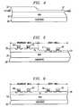
- FIG. 1is a typical DRAM memory array which shows a separate pass transistor 20 associated with each memory cell 22 .
- Word lines WL and bit lines BLare also attached to each pass transistor 20 in a known manner.
- each DRAMalso has peripheral area outside the memory array.
- the peripheral areaincludes various logic circuits including for example address decoding circuits, wordline drivers, sense amplifiers, and input/output circuits.
- FIGS. 2-4illustrate a process flow for a silicon on insulator (SOI) structure wherein the silicon layer is thinner in the memory array area than it is in the peripheral area of the DRAM.
- the first stepis to provide a silicon-on-insulator structure comprised of silicon layer 33 on an oxide layer 32 which is on a substrate 30 .
- This SOI structurecan be fabricated in any of a variety of known processes such as bonding with etch back, SIMOX, or epitaxial lateral overgrowth.
- the thickness of silicon layer 33is desired to be approximately 60 nm or greater to provide for partially depleted transistors in the periphery area.
- a nitride layer 35 on top of a pad oxide layer 34is used to mask the periphery area from the array area.
- the exposed array areais oxidized to form SiO 2 layer 36 .
- the SiO 2 layer 36 , the nitride mask 35 and pad oxide 34are removed leaving the structure shown in FIG. 4 .
- the silicon in the memory array areahas been selectively thinned to provide a thickness t si of approximately 30-80 nm. This thickness should provide for fully depleted pass transistors in the memory array area upon further processing.
- Alternate means of obtaining seletively different silicon film thickness for pass and periphery transistorsinclude the use of selective epi, and bonding with a selectively contoured device wafer. For the latter, various means of contouring can be used, including selective oxidation and etching. Use of bonding with a selectively contoured device wafer has the advantage of presenting a substantially planar surface for subsequent processing.(See U.S. Pat. No. 5,436,173).
- a plurality of pass transistors 40 and 41are formed in the array area and a plurality of logic transistors 42 and 43 are formed in the periphery of the DRAM. Selected peripheral transistors may also be formed in areas of thinner silicon.
- the plurality of transistors 41 and 42are formed in accordance with normal processing except that p-doped polysilicon is used in the gate material of the n-channel pass transistors in the array area instead of n doped polysilicon of the prior art.
- the p-doped polysilicon gate materialis chosen to have a higher work function than the standard n-doped polysilicon gate for the n-channel pass transistor.
- an n-doped polysilicon doped gate materialwould be used to provide the higher threshold voltage.
- a metal such as tungsten or titanium nitridecould be chosen to give a higher gate threshold voltage for the pass transistors, than the prior art.
- Multilayer gate materialmay be used to get the desired work function combined with other desired characteristics.
- p-doped polymay be layered with tungsten to reduce resistance, or TiN may be layered with n-doped polysilicon.
- the silicon layer 37 in the array areacould be either fully depleted or partially depleted depending on the exact doping and Si film thickness t si . It is preferable to use a thin silicon film (less than 80 mm) for reduced junction area, leading to a fully depleted channel for the pass gate transistors of the array area.
- FIG. 6An SOI structure with a plurality of pass transistors 45 and 46 in the array area and a plurality of logic transistors 47 and 48 in the periphery of the DRAM is shown in FIG. 6 .
- One less lithography stepwould be required to produce the SOI structure in FIG. 6 as compared to the SOI structure of FIG. 5 due to uniform layer 38 providing a uniform silicon film thickness t si for all transistors throughout the DRAM device.
- a DRAM having a uniform silicon channel thickness t si of 60 mmin accordance with FIG. 6, wherein the pass and periphery transistors use n-doped polysilicon gates for all transistors in the first example and p-doped polysilicon gates for all transistors in the second and third examples given below.
- the p-channel pass transistorhas an advantage relative to the n-channel pass for SOI because of the lower parasitic bipolar gain for a p-n-p structure vs a n-p-n structure. Also, if opposite gate doping is used (n-poly for p-channel or p-poly for n-channel) the n-poly gate of the p-channel pass transistor has the advantage of lower resistance. Further, as gate oxides are thinned, n-poly will have an advantage of not needing to be concerned with boron penetration through the gate oxide as would be the case for p-poly.
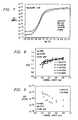
- FIG. 7shows the I-V characteristics of a fully depleted SOI DRAM pass transistor with p+gate design.
- the Vth implantwas BF 2 , 40 KeV, 8E11 dose.
- the LDD implantwas As, 40KeV, 3E14 dose and the p+ gate was formed by 10KeV, 3E15 dose Boron implant and annealed during the junction sequence.
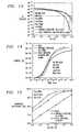
- FIG. 8shows the linear V th of DRAM pass transistors for various SOI film thicknesses using p+ gate design.
- the Vth implant for all the transistorsis BF 2 , 40 KeV, 1E12 dose and the LDD implant is As, 40KeV, 4E13 dose, and the channel width is 1.0 um.
- the V th of the transistorsis 1.1 ⁇ 1.2V and does not change significantly as the SOI film thickness varies. The short channel effect on these transistors is also very small, due to the thin SOI film thicknesses.
- the V th roll-offis larger and is a function of the SOI film thicknesses, shown in FIG. 10 .
- Vtdepends on Si film thickness, adding another source of Vt variation. But with the very low channel doping with opposite gate type, this variation is very small. Further, the variation of Vt with temperature is smaller for fully depleted SOI than for partially depleted or bulk.
- the body potential of the partially depleted SOI transistorswill follow the source node potential during the charging because of the floating body effect, so that the body to source potential difference is kept at a substantially constant value. For fully depleted SOI transistors, there is no body potential change since the channel is fully depleted through the entire silicon-filmed thickness. Therefore, the SOI transistors will have a higher charging efficiency compared to the bulk transistors.
- FIG. 13shows the channel current as a function of source node voltage for the bulk and SOI transistors.
- the charging efficiencydefined as the ratio of source voltage at 1 mm to the drain voltage (the bitline voltage)
- the charging efficiencyis 80% for bulk transistors and 88% and 98% for partially and fully depleted SOI transistors, respectively.
- the higher charging efficiency of SOIshows charging characteristics of a 25 fF capacitor.
- the bulk transistorshows a faster charging at below 0.1 ns due to its higher initial current.
- the SOI transistorsshow faster charging characteristics for time greater than 0.1 ns.
- the fully depleted SOI transistorcan charge ten times more charge than bulk transistor at ins, which is the typical charging time for a DRAM cell.
- FIG. 15shows the charging efficiency as a function of gate voltage for the bulk and SOI DRAM pass transistors.
- the gate voltage of the bulk transistorhas to be 0.6 V higher than that of thin film SOI transistors.
- the increased wordline voltagewill worsen the gate oxide integrity and is also not favorable for the low power operation.
Landscapes
- Engineering & Computer Science (AREA)
- Manufacturing & Machinery (AREA)
- Semiconductor Memories (AREA)
- Thin Film Transistor (AREA)
Abstract
Description
This application is a division of application Ser. No. 08/862,449, filed May 23, 1997 U.S. Pat. No. 6,424,016, which claims priority to provisional Application No. 60/018,300, filed May 24, 1996.
1. Field of the Invention
This invention relates to a the design of DRAMs using Silicon on Insulator (SOI) technology and more particularly to the design of fully depleted memory pass transistors in the DRAM in combination with a P-doped polysilicon gate.
2. Description of the Prior Art
SOI is good for DRAM for several reasons. One reason is that SOI has lower collection volume for charge generated by an alpha particle or a cosmic ray. Such charge can upset the memory cell, so the smaller collection volume of SOI is desirable. SOI also reduces the capacitance on the bit line so less charge is needed to generate an equivalent signal on the bit line relative to bulk DRAM. Also reduced junction area in the memory cell should give lower leakage which translates to longer retention time. All these features, lower collection volume, lower leakage and lower capacitance, are advantages of SOI.
There are also potential difficulties in using SOI for DRAM. These include cost, yield, and floating body effects. SOI wafers cost more than bulk silicon wafers, so it is important to keep the SOI processing cost low. Yield on SOI wafers is expected to improve as the material quality continues to be improved. Floating body effects can improve performance for logic circuits, but can also amplify collected charge (as from alpha particle strikes) or increase leakage currents. So there is a need for a low cost SOI process with reduced floating body effects.
The basic memory cell in a DRAM is a pass and a storage element (capacitor). The full DRAM includes an array of memory cells, and peripheral circuitry to control storage and retrieval of data into and from the memory array. The DRAM may be included with other circuitry in an integrated circuit. The process for a DRAM must encompass the requirements for the memory array pass gate and the peripheral transistors. The requirements for the pass gate transistor distinguish the design of transistors for DRAMs from logic or SRAMs. The pass gate must have very low leakage. This requires relatively high threshold voltage. It is also desirable for the pass gate transistor to have low source capacitance to help keep the bit line capacitance low. For charge transfer, it is usual to have a boosted word line voltage, which leads to thicker gate oxide for reliability. The pass gate transistor does not need to have high drive current. The pass gate transistor is usually N channel with an N doped polysilicon gate. There are some advantages to N polysilicon and the N channel has higher drive because of the higher mobility of electrons.
Peripheral transistors have requirements similar to standard logic transistors. They generally will be designed with lower VT than the pass transistor. But to reduce cost, it is usual to have the peripheral transistor with the same gate oxide and single N polysilicon that is used for the pass transistor. Also silicide is not used to reduce cost.
Thus the design requirements for the peripheral transistor of a DRAM also may be different from the usual design requirements for standard logic. Nevertheless, we will sometimes refer to the DRAM peripheral transistors as logic transistors.
There are different types of SOI transistors, and the choice of the SOI transistor type will affect the SOI DRAM performance. SOI transistors can be classified as fully depleted or partially depleted. Some SOI transistors may also be classified as nearly fully depleted. These are fully depleted when on and partially depleted when off. For a given channel doping SOI transistors go from partially depleted to fully depleted as the silicon film thickness is thinned. The partially depleted transistor characteristics, including determination of threshold voltage, are very much like bulk transistors except for the floating body effects. Fully depleted transistors have some unique characteristics, and have reduced floating body effects. For fully depleted transistors, the range of threshold voltage is limited by the gate work function and silicon film thickness. As the channel doping is increased to increase the threshold voltage the transistor transitions from fully depleted to partially depleted. There is an upper limit of threshold voltage for fully depleted SOI transistors for a given silicon film thickness and gate work function. For logic, it has been proposed to use a mid band-gap work function to raise the threshold voltage of both n and p-channel transistors. Polysilicon gate with “opposite” doping (p type for n-channel and n type for p-channel) has also been proposed combined with accumulation transistor mode design to get suitable threshold voltages for logic or SRAM circuits.
In addition to the difficulty of selecting desirable threshold voltage, fully depleted transistors suffer from higher source/drain resistance because of the thinner silicon film. This is particularly true when silicide is used since there is high contact resistance if the silicide consumes the full silicon film thickness. For these reasons most commercial work on SOI, including work on SOI DRAM, has emphasized partially depleted transistors.(See H. S. Kim et al. 1995 Synmposium on VLSI Technology Digest of Technical Papers pp. 143, 1995)
For SOI DRAM, the thinner silicon film associated with fully depleted or near fully depleted transistors has several advantages. These include a smaller junction area leading to smaller junction leakage and smaller junction capacitance. The thinner silicon film also provides a smaller volume for charge generation from ion strikes. The fully depleted transistor also has reduced floating body effects that can increase leakage in pass transistors and lead to variation of threshold voltages which would be deleterious to sense amplifiers. Further, the higher series resistance of fully depleted transistors is not significant in the DRAM array, especially since silicide is generally not used. However, the threshold voltage of a fully depleted n-channel SOI transistor with n-poly gate is too low for DRAM pass transistor application.
It is therefore a general object of the present invention to design an SOI pass transistor for a DRAM that has a high threshold voltage and reduced floating body effects.
It is a further object of the present invention to integrate the above DRAM pass gate transistor with peripheral transistors with suitable characteristics.
These and other objects of the invention will become apparent to those of ordinary skill in the art having reference to the following specification, in conjunction with the drawings.
In this invention, the gate material is chosen to have a higher work function to increase the threshold voltage of the DRAM array pass transistor relative to the use of n-poly for n-channel transistors. This reduces the floating body induced leakage under dynamic conditions. This also allow the use of fully depleted or nearly fully depleted transistors in the array. These can be combined with fully depleted transistors in the periphery. Alternatively, a different thickness silicon film can be used in the array verses in the periphery, such as by selective thinning, to allow fully depleted transistors in the array and partially depleted transistors in the periphery. The use of SOI transistors in the array and bulk transistors in the periphery is also possible.
In a preferred embodiment the pass transistors are fully depleted P channel transistors operating in the inversion mode with N type polysilicon gates. The periphery has fully depleted P channel accumulation mode transistors with N doped polysilicon gates and fully depleted N channel inversion mode transistors also with N type polysilicon gates.
In another embodiment, the pass transistors are fully depleted N channel inversion mode transistors with P type polysilicon gates, wherein the periphery transistors are fully depleted N channel accumulation mode transistors with P type polysilicon gates in addition to fully depleted P channel inversion mode transistors also with P type polysilicon gates.
In another embodiment, the pass transistors are fully depleted P channel inversion mode transistors with N type polysilicon gates. The peripheral transistors are partially depleted P channel inversion mode transistors with N type polysilicon gates in addition to partially depleted N channel inversion mode transistors with N type polysilicon gates. The pass transistors are made with thinner silicon film than the peripheral transistors. Optionally some of the peripheral transistors such as in the sense amps may also be fully depleted.
In yet another embodiment the silicon insulator and bulk transistors are used on the same integrated circuit. This would be done with masked SIMOX or by other techniques, such as epitaxial lateral overgrowth. Here the transistors in the array would be made fully depleted with SOI and the peripheral transistors would be fabricated in bulk silicon. Selectively, some of the peripheral transistors could also be put on SOI.
FIG. 1 is an illustration of a prior art DRAM memory array;
FIGS. 2-4 show a process flow for arriving at a SOI structure having a thinner silicon area in the array area than in the periphery area;
FIG. 5 shows one preferred embodiment of the current invention;
FIG. 6 shows an alternate preferred embodiment of the current invention;
FIG. 7 shows the I-V characteristics of a fully depleted SOI DRAM pass transistor;
FIG. 8 shows the linear threshold voltage of SOI DRAM pass transistors with various starting SOI film thicknesses.
FIG. 9 shows the subthreshold leakage current, Ioff, of SOI DRAM pass transistors on two different starting SO films;
FIG. 10 shows the saturation Vth of SOI DRAM pass transistors with various starting SOI film thicknesses;
FIG. 11 shows the linear Vth of SOI DRAM pass transistors with various starting SOI film thicknesses;
FIG. 12 shows the subthreshold leakage current, Ioff, of SOI DRAM pass transistor swith various starting film thicknesses;
FIG. 13 shows the channel current as a function of source node voltage for bulk and SOI DRAM pass transistors;
FIG. 14 shows the charging characteristics of a 25 fF capacitor for bulk and SOI DRAM pass transistors; and
FIG. 15 shows the charging efficiency as a function of gate voltage for bulk and SOI DRAM pass transistors.
FIG. 1 is a typical DRAM memory array which shows aseparate pass transistor 20 associated with eachmemory cell 22. Word lines WL and bit lines BL are also attached to eachpass transistor 20 in a known manner. In addition to the memory array as shown in FIG. 1 each DRAM also has peripheral area outside the memory array. The peripheral area includes various logic circuits including for example address decoding circuits, wordline drivers, sense amplifiers, and input/output circuits.
FIGS. 2-4 illustrate a process flow for a silicon on insulator (SOI) structure wherein the silicon layer is thinner in the memory array area than it is in the peripheral area of the DRAM. In FIG. 2, the first step is to provide a silicon-on-insulator structure comprised ofsilicon layer 33 on anoxide layer 32 which is on asubstrate 30. This SOI structure can be fabricated in any of a variety of known processes such as bonding with etch back, SIMOX, or epitaxial lateral overgrowth. The thickness ofsilicon layer 33 is desired to be approximately 60 nm or greater to provide for partially depleted transistors in the periphery area. Anitride layer 35 on top of apad oxide layer 34 is used to mask the periphery area from the array area. As shown in FIG. 3, the exposed array area is oxidized to form SiO2layer36. The SiO2layer36, thenitride mask 35 andpad oxide 34 are removed leaving the structure shown in FIG.4. The silicon in the memory array area has been selectively thinned to provide a thickness tsiof approximately 30-80 nm. This thickness should provide for fully depleted pass transistors in the memory array area upon further processing. Alternate means of obtaining seletively different silicon film thickness for pass and periphery transistors include the use of selective epi, and bonding with a selectively contoured device wafer. For the latter, various means of contouring can be used, including selective oxidation and etching. Use of bonding with a selectively contoured device wafer has the advantage of presenting a substantially planar surface for subsequent processing.(See U.S. Pat. No. 5,436,173).
As shown in FIG. 5, after processing of the SOI structure, with thinned silicon for fully depleted transistors in the array area, a plurality ofpass transistors logic transistors transistors
Instead of using the p-doped polysilicon gate material a metal such as tungsten or titanium nitride (having a near mid-gap work function) could be chosen to give a higher gate threshold voltage for the pass transistors, than the prior art. Multilayer gate material may be used to get the desired work function combined with other desired characteristics. For example, p-doped poly may be layered with tungsten to reduce resistance, or TiN may be layered with n-doped polysilicon.
With the SOI structure shown in FIG. 5, thesilicon layer 37 in the array area could be either fully depleted or partially depleted depending on the exact doping and Si film thickness tsi. It is preferable to use a thin silicon film (less than 80 mm) for reduced junction area, leading to a fully depleted channel for the pass gate transistors of the array area.
For optimal performance of the pass transistors in the array area and the logic transistors in the periphery, different gate material and/or different film thickness could be used in the array vs. the periphery, as illustrated in FIG.5 and discussed above. This is because the transistors in both areas can be optimized independently.
However, for optimal processing efficiency, the same gate material and film thickness tsiwould be used for both the array area and periphery to reduce cost. An SOI structure with a plurality ofpass transistors logic transistors uniform layer 38 providing a uniform silicon film thickness tsifor all transistors throughout the DRAM device. Following are three examples of a DRAM having a uniform silicon channel thickness tsiof 60 mm, in accordance with FIG. 6, wherein the pass and periphery transistors use n-doped polysilicon gates for all transistors in the first example and p-doped polysilicon gates for all transistors in the second and third examples given below.
Uniform thickness for Silicon channel: 60 mm
Single gate material: n+ polysilicon
(1) Pass transistors: fully depleted p-channel transistors with 1E17 n type doping in channel. (Vt=˜−1.2V)
(2) n-channel periphery transistors: partially depleted transistors with 6E17 p type doping in channel. (Vt=˜0.5V)
(3) p-channel periphery transistors: fully depleted transistors with 3E16 p type doping in channel. (accumulation mode, Vt=˜−0.5V)
Uniform thickness for Silicon channel: 60 mm
Single gate material: P+polysilicon
(1) Pass transistors: fully depleted n-channel transistors with 1E17 p type doping in channel. (Vt=˜1.2V)
(2) n-channel periphery transistors: fully depleted transistors with 3E16 n type doping in channel. (Accumulation mode, Vt=˜0.5V)
(3) p-channel periphery transistors: partially depleted transistors with 6E17 n type doping in channel. (Vt=˜−0.5V)
Uniform thickness for Silicon channel: 60 mm
Single gate material: p+polysilicon
(1) Pass transistors: fully depleted n-channel transistors with 1E16 n type doping in channel. (Accumulation mode, Vt=˜0.8V)
(2) n-channel periphery transistors: fully depleted transistors with 3E16 n type doping in channel. (Accumulation mode, Vt=˜−0.5V)
(3) p-channel periphery transistors: partially depleted transistors with 6E17 n type doping in channel. (Vt=˜−0.5V)
As stated above, it is possible to have fully depleted pass transistors in the array and partially depleted logic transistors in the periphery using different silicon film thicknesses. Another option is to use different gate materials. An example of this is as follows:
Uniform thickness for Silicon channel: 60 nm
(1) Pass transistors: fully depleted p-channel transistors having n-doped poly gates with 1E17 n type doping in channel. (Vt=˜−1.2V)
(2) n-channel periphery transistors: partially depleted transistors having n-doped poly gates with 6E17 p type doping in channel. (Vt=˜0.5V)
(3) p-channel periphery transistors: partially depleted transistors having p-doped poly gates with 6E17 n type doping in channel. (Vt=˜−0.5V)
It should be recognized that the above examples were given knowing that the devices can be optimized with channel profiling and source/drain engineering. Therefore, the invention is not intended to be limited to the above examples.
The p-channel pass transistor has an advantage relative to the n-channel pass for SOI because of the lower parasitic bipolar gain for a p-n-p structure vs a n-p-n structure. Also, if opposite gate doping is used (n-poly for p-channel or p-poly for n-channel) the n-poly gate of the p-channel pass transistor has the advantage of lower resistance. Further, as gate oxides are thinned, n-poly will have an advantage of not needing to be concerned with boron penetration through the gate oxide as would be the case for p-poly.
Both partially and fully depleted pass transistors were designed and fabricated on SIMOX substrates. Using a p+gate design, Vth=1V and Ioff<1 fA/mm was achieved for ultra thin film SOI pass transistors. With less than 1 fA/mm off-state leakage design, the SOI pass transistor should provide excellent DRAM cell retention time and low stand-by power. In addition, the SOI pass transistors were found to have a high DRAM charging efficiency (>80% for partially depleted devices and >95% for fully depleted devices) than the bulk pass transistor (80%) because of the elimination of the body effect. The higher charging efficiency allows SOI pass transistors to reduce the wordline voltage during the charging state, increase the gate oxide integrity and decrease the active power.
FIG. 7 shows the I-V characteristics of a fully depleted SOI DRAM pass transistor with p+gate design. The Vth implant was BF2, 40 KeV, 8E11 dose. The LDD implant was As, 40KeV, 3E14 dose and the p+ gate was formed by 10KeV, 3E15 dose Boron implant and annealed during the junction sequence. FIG. 8 shows the linear Vthof DRAM pass transistors for various SOI film thicknesses using p+ gate design. The Vth implant for all the transistors is BF2, 40 KeV, 1E12 dose and the LDD implant is As, 40KeV, 4E13 dose, and the channel width is 1.0 um. The subthreshold leakage current, Ioff, at Vds=2.5V of these transistors is shown in FIG.9. As shown in the FIG. 8, the Vthof the transistors is 1.1˜1.2V and does not change significantly as the SOI film thickness varies. The short channel effect on these transistors is also very small, due to the thin SOI film thicknesses. The leakage current I at Vds=2.5V is below 1 fA/mm, which would improve the retention of the DRAM cell and reduce the stand-by power significantly. In the saturation condition, the Vthroll-off is larger and is a function of the SOI film thicknesses, shown in FIG.10. For a comparison, all the n+ gate design n-channel transistors have Vthbelow 0.6V and Ioffis on the order of nA/mm. FIG.11 and FIG. 12 show the Vthand Ioffof n+ gate transistors as a function of SOI film thicknesses. As the SOI film thickness is larger than 60 mm, the subthreshold slope of the devices at Vds=2.5V is less than 70 mV/dec which is an indication that the devices are partially depleted.
It is commonly considered a draw back of fully depleted SOI that the Vt depends on Si film thickness, adding another source of Vt variation. But with the very low channel doping with opposite gate type, this variation is very small. Further, the variation of Vt with temperature is smaller for fully depleted SOI than for partially depleted or bulk.
The bulk pass transistors suffer from the increase in Vt threshold voltage caused by the body effect during the capacitor charging state, so the wordline voltage has to be boosted to VWL=Vth+Vds+_V, where _V compensates for the Vthincreasing during the charging. Reducing the body effect becomes a major issue in bulk pass transistor design. On the other hand, the body potential of the partially depleted SOI transistors will follow the source node potential during the charging because of the floating body effect, so that the body to source potential difference is kept at a substantially constant value. For fully depleted SOI transistors, there is no body potential change since the channel is fully depleted through the entire silicon-filmed thickness. Therefore, the SOI transistors will have a higher charging efficiency compared to the bulk transistors. FIG. 13 shows the channel current as a function of source node voltage for the bulk and SOI transistors. If the charging current is designed to be 1 mA/mm, then the charging efficiency, defined as the ratio of source voltage at 1 mm to the drain voltage (the bitline voltage), the charging efficiency is 80% for bulk transistors and 88% and 98% for partially and fully depleted SOI transistors, respectively. The higher charging efficiency of SOI shows charging characteristics of a 25 fF capacitor. The bulk transistor shows a faster charging at below 0.1 ns due to its higher initial current. The SOI transistors show faster charging characteristics for time greater than 0.1 ns. The fully depleted SOI transistor can charge ten times more charge than bulk transistor at ins, which is the typical charging time for a DRAM cell. For the bulk pass transistors to reach the same charging efficiency as SOI transistors, one has to increase the wordline voltage during the charging. FIG. 15 shows the charging efficiency as a function of gate voltage for the bulk and SOI DRAM pass transistors. To reach 90% charging efficiency, the gate voltage of the bulk transistor has to be 0.6 V higher than that of thin film SOI transistors. The increased wordline voltage will worsen the gate oxide integrity and is also not favorable for the low power operation.
In summary, we have demonstrated a p+ gate SOI DRAM pass transistor design on ultra thin SOI films which has below 1 fA/mm subthreshold leakage current. In addition, we have shown that the fully depleted SOI pass transistors have higher charging efficiency compared to bulk pass transistors. The higher charging efficiency allows SOI pass transistors to reduce the wordline voltage during the charging state and increase the gate oxide integrity. By using a p+ gate design for the pass transistors of the DRAM, we have achieved less than 1 fA/mm of subthreshold leakage current on ultra thin SOI film thicknesses ranging from 400A to 800A.
While the invention has been shown and described with respect to particular embodiments, it will be understood by those skilled in the art that the foregoing and other changes in form and detail may be made therein without departing from the spirit and scope of the invention.
Claims (13)
1. An integrated circuit including a dynamic random access memory circuit comprising:
a memory array including a plurality of pass gate transistors and a plurality of memory elements, wherein said pass gate transistors comprise devices having a first conductivity type channel and gate regions having a second conductivity type, wherein said pass gate transistors have fully depleted channel regions; and
a peripheral area including a plurality of logic transistors wherein said logic transistors have partially depleted channel regions.
2. The integrated circuit ofclaim 1 wherein said pass gate transistors are p-channel transistors with N+ doped polysilicon gate regions.
3. The integrated circuit ofclaim 2 wherein said N+ doped polysilicon gate regions are clad with a metal layer.
4. The integrated circuit ofclaim 3 wherein said metal layer comprises tungsten.
5. The integrated circuit ofclaim 2 wherein a silicide layer is formed on said N+ polysilicon gate regions.
6. An integrated circuit including a dynamic random access memory circuit comprising:
a memory array including a plurality of pass gate transistors and a plurality of memory elements, wherein said pass gate transistors comprise devices having a first conductivity type channel and gate regions having a second conductivity type; and
a peripheral area including a plurality of logic transistors;
wherein said pass gate transistors are p-channel transistors with N+ doped polysilicon gate regions.
7. The integrated circuit ofclaim 6 wherein said N+ doped polysilicon gate regions are clad with a metal layer.
8. The integrated circuit ofclaim 7 wherein said metal layer comprises tungsten.
9. The integrated circuit ofclaim 6 wherein a silicide layer is formed on said N+ polysilicon gate regions.
10. An integrated circuit including a dynamic random access memory circuit comprising:
a memory array including a plurality of pass gate transistors and a plurality of memory elements, wherein said pass gate transistors comprise devices having a first conductivity type channel and gate regions having a second conductivity type; and
a peripheral area including a plurality of logic transistors;
wherein said pass gate transistors are silicon on insulator transistors.
11. An integrated circuit including a dynamic random access memory circuit comprising:
a memory array including a plurality of pass gate transistors and a plurality of memory elements, wherein said pass gate transistors comprise devices having a first conductivity type channel and gate regions having a second conductivity type; and
a peripheral area including a plurality of logic transistors;
wherein a gate material of said pass gate transistors is different from a gate material of said logic transistors.
12. An integrated circuit including a dynamic random access memory circuit comprising:
a memory array including a plurality of pass gate transistors and a plurality of memory elements, wherein said pass gate transistors comprise devices having a first conductivity type channel and gate regions having a second conductivity type; and
a peripheral area including a plurality of logic transistors;
wherein a gate material of said pass gate transistors is a different thickness from a gate material of said logic transistors.
13. An integrated circuit including a dynamic random access memory circuit comprising:
a memory array including a plurality of pass gate transistors and a plurality of memory elements, wherein said pass gate transistors comprise devices having a first conductivity type channel and gate regions having a second conductivity type; and
a peripheral area including a plurality of logic transistors;
wherein said pass gate transistors have respective channel regions and said gate regions have a work function near the middle of the band gap of said channel regions.
Priority Applications (1)
| Application Number | Priority Date | Filing Date | Title |
|---|---|---|---|
| US10/142,336US6703673B2 (en) | 1996-05-24 | 2002-05-09 | SOI DRAM having P-doped poly gate for a memory pass transistor |
Applications Claiming Priority (3)
| Application Number | Priority Date | Filing Date | Title |
|---|---|---|---|
| US1830096P | 1996-05-24 | 1996-05-24 | |
| US08/862,449US6424016B1 (en) | 1996-05-24 | 1997-05-23 | SOI DRAM having P-doped polysilicon gate for a memory pass transistor |
| US10/142,336US6703673B2 (en) | 1996-05-24 | 2002-05-09 | SOI DRAM having P-doped poly gate for a memory pass transistor |
Related Parent Applications (1)
| Application Number | Title | Priority Date | Filing Date |
|---|---|---|---|
| US08/862,449DivisionUS6424016B1 (en) | 1996-05-24 | 1997-05-23 | SOI DRAM having P-doped polysilicon gate for a memory pass transistor |
Publications (2)
| Publication Number | Publication Date |
|---|---|
| US20020180069A1 US20020180069A1 (en) | 2002-12-05 |
| US6703673B2true US6703673B2 (en) | 2004-03-09 |
Family
ID=26690954
Family Applications (2)
| Application Number | Title | Priority Date | Filing Date |
|---|---|---|---|
| US08/862,449Expired - LifetimeUS6424016B1 (en) | 1996-05-24 | 1997-05-23 | SOI DRAM having P-doped polysilicon gate for a memory pass transistor |
| US10/142,336Expired - LifetimeUS6703673B2 (en) | 1996-05-24 | 2002-05-09 | SOI DRAM having P-doped poly gate for a memory pass transistor |
Family Applications Before (1)
| Application Number | Title | Priority Date | Filing Date |
|---|---|---|---|
| US08/862,449Expired - LifetimeUS6424016B1 (en) | 1996-05-24 | 1997-05-23 | SOI DRAM having P-doped polysilicon gate for a memory pass transistor |
Country Status (1)
| Country | Link |
|---|---|
| US (2) | US6424016B1 (en) |
Cited By (48)
| Publication number | Priority date | Publication date | Assignee | Title |
|---|---|---|---|---|
| US20040121547A1 (en)* | 2002-12-18 | 2004-06-24 | Lee Dae Woo | Structures of high voltage device and low voltage device, and method of manufacturing the same |
| US20050133843A1 (en)* | 2003-11-21 | 2005-06-23 | Kabushiki Kaisha Toshiba | Semiconductor device and method of manufacturing a semiconductor device |
| US20070257291A1 (en)* | 2006-05-02 | 2007-11-08 | Serguei Okhonin | Semiconductor memory cell and array using punch-through to program and read same |
| US20070297252A1 (en)* | 2006-06-26 | 2007-12-27 | Anant Pratap Singh | Integrated circuit having memory array including ECC and/or column redundancy, and method of programming, controlling and/or operating same |
| US20080013359A1 (en)* | 2006-07-11 | 2008-01-17 | David Fisch | Integrated circuit including memory array having a segmented bit line architecture and method of controlling and/or operating same |
| US20080180995A1 (en)* | 2007-01-26 | 2008-07-31 | Serguei Okhonin | Semiconductor Device With Electrically Floating Body |
| US20080237714A1 (en)* | 2007-03-29 | 2008-10-02 | Pierre Fazan | Manufacturing Process for Zero-Capacitor Random Access Memory Circuits |
| US20080298139A1 (en)* | 2007-05-30 | 2008-12-04 | David Fisch | Integrated circuit having voltage generation circuitry for memory cell array, and method of operating and /or controlling same |
| US20090016101A1 (en)* | 2007-06-01 | 2009-01-15 | Serguei Okhonin | Reading Technique for Memory Cell With Electrically Floating Body Transistor |
| US20090080244A1 (en)* | 2007-09-17 | 2009-03-26 | Eric Carman | Refreshing Data of Memory Cells with Electrically Floating Body Transistors |
| US20090141550A1 (en)* | 2006-04-07 | 2009-06-04 | Eric Carman | Memory Array Having a Programmable Word Length, and Method of Operating Same |
| US20090146219A1 (en)* | 2007-12-11 | 2009-06-11 | Danngis Liu | Integrated circuit having memory cell array, and method of manufacturing same |
| US20090200612A1 (en)* | 2008-02-08 | 2009-08-13 | Viktor Koldiaev | Integrated Circuit Having Memory Cells Including Gate Material Having High Work Function, and Method of Manufacturing Same |
| US20090225579A1 (en)* | 2007-11-05 | 2009-09-10 | Shepard Daniel R | Low cost, high-density rectifier matrix memory |
| US20090251958A1 (en)* | 2008-04-04 | 2009-10-08 | Philippe Bauser | Read circuitry for an integrated circuit having memory cells and/or a memory cell array, and method of operating same |
| US20090302387A1 (en)* | 2006-04-07 | 2009-12-10 | International Business Machines Corporation | Integrated circuit chip with fets having mixed body thicknesses and method of manufacture thereof |
| US20100075471A1 (en)* | 2008-09-25 | 2010-03-25 | Innovative Silicon Isi Sa | Recessed Gate Silicon-On-Insulator Floating Body Device With Self-Aligned Lateral Isolation |
| US20100085806A1 (en)* | 2008-10-02 | 2010-04-08 | Ping Wang | Techniques for reducing a voltage swing |
| US20100091586A1 (en)* | 2008-10-15 | 2010-04-15 | Innovative Silicon Isi Sa | Techniques for simultaneously driving a plurality of source lines |
| US20100110816A1 (en)* | 2008-11-05 | 2010-05-06 | Innovative Silicon Isi Sa | Techniques for block refreshing a semiconductor memory device |
| US20100210075A1 (en)* | 2009-02-18 | 2010-08-19 | Innovative Silicon Isi Sa | Techniques for providing a source line plane |
| US20100224924A1 (en)* | 2009-03-04 | 2010-09-09 | Innovative Silicon Isi Sa | Techniques for forming a contact to a buried diffusion layer in a semiconductor memory device |
| US20100259964A1 (en)* | 2009-03-31 | 2010-10-14 | Innovative Silicon Isi Sa | Techniques for providing a semiconductor memory device |
| US20100271858A1 (en)* | 2009-04-27 | 2010-10-28 | Innovative Silicon Isi Sa | Techniques for providing a direct injection semiconductor memory device having ganged carrier injection lines |
| US7826244B2 (en) | 2000-06-22 | 2010-11-02 | Contour Semiconductor, Inc. | Low cost high density rectifier matrix memory |
| US20100277982A1 (en)* | 2009-04-30 | 2010-11-04 | Innovative Silicon Isi Sa | Semiconductor device with floating gate and electrically floating body |
| US20110007578A1 (en)* | 2009-07-10 | 2011-01-13 | Innovative Silicon Isi Sa | Techniques for providing a semiconductor memory device |
| US20110019479A1 (en)* | 2009-07-27 | 2011-01-27 | Innovative Silicon Isi Sa | Techniques for providing a direct injection semiconductor memory device |
| US20110037103A1 (en)* | 2009-08-14 | 2011-02-17 | Renesas Electronics Corporation | Semiconductor device and method of manufacturing the same |
| US20110058436A1 (en)* | 2009-09-04 | 2011-03-10 | Innovative Silicon Isi Sa | Techniques for sensing a semiconductor memory device |
| US20110141836A1 (en)* | 2009-12-16 | 2011-06-16 | Innovative Silicon Isi Sa | Techniques for reducing impact of array disturbs in a semiconductor memory device |
| US20110199848A1 (en)* | 2010-02-12 | 2011-08-18 | Innovative Silicon Isi Sa | Techniques for controlling a semiconductor memory device |
| US8014195B2 (en) | 2008-02-06 | 2011-09-06 | Micron Technology, Inc. | Single transistor memory cell |
| US20110216617A1 (en)* | 2010-03-04 | 2011-09-08 | Innovative Silicon Isi Sa | Techniques for sensing a semiconductor memory device |
| US20110216608A1 (en)* | 2010-03-05 | 2011-09-08 | Innovative Silicon Isi Sa | Techniques for reading from and/or writing to a semiconductor memory device |
| US20110216605A1 (en)* | 2010-03-04 | 2011-09-08 | Innovative Silicon Isi Sa | Techniques for providing a semiconductor memory device having hierarchical bit lines |
| US8174881B2 (en) | 2009-11-24 | 2012-05-08 | Micron Technology, Inc. | Techniques for reducing disturbance in a semiconductor device |
| US8213226B2 (en) | 2008-12-05 | 2012-07-03 | Micron Technology, Inc. | Vertical transistor memory cell and array |
| US8411524B2 (en) | 2010-05-06 | 2013-04-02 | Micron Technology, Inc. | Techniques for refreshing a semiconductor memory device |
| US8498157B2 (en) | 2009-05-22 | 2013-07-30 | Micron Technology, Inc. | Techniques for providing a direct injection semiconductor memory device |
| US8531878B2 (en) | 2011-05-17 | 2013-09-10 | Micron Technology, Inc. | Techniques for providing a semiconductor memory device |
| US8536628B2 (en) | 2007-11-29 | 2013-09-17 | Micron Technology, Inc. | Integrated circuit having memory cell array including barriers, and method of manufacturing same |
| US8547738B2 (en) | 2010-03-15 | 2013-10-01 | Micron Technology, Inc. | Techniques for providing a semiconductor memory device |
| US8773933B2 (en) | 2012-03-16 | 2014-07-08 | Micron Technology, Inc. | Techniques for accessing memory cells |
| US8873283B2 (en) | 2005-09-07 | 2014-10-28 | Micron Technology, Inc. | Memory cell and memory cell array having an electrically floating body transistor, and methods of operating same |
| US9559216B2 (en) | 2011-06-06 | 2017-01-31 | Micron Technology, Inc. | Semiconductor memory device and method for biasing same |
| US20180151448A1 (en)* | 2016-11-29 | 2018-05-31 | Taiwan Semiconductor Manufacturing Company, Ltd. | Breakdown resistant semiconductor apparatus and method of making same |
| US10163303B1 (en) | 2013-03-13 | 2018-12-25 | PlayStudios, Inc. | Cash slot machine augmented with secondary currency |
Families Citing this family (246)
| Publication number | Priority date | Publication date | Assignee | Title |
|---|---|---|---|---|
| US6537891B1 (en)* | 2000-08-29 | 2003-03-25 | Micron Technology, Inc. | Silicon on insulator DRAM process utilizing both fully and partially depleted devices |
| TWI230392B (en)* | 2001-06-18 | 2005-04-01 | Innovative Silicon Sa | Semiconductor device |
| US6952040B2 (en)* | 2001-06-29 | 2005-10-04 | Intel Corporation | Transistor structure and method of fabrication |
| JP2003031684A (en)* | 2001-07-11 | 2003-01-31 | Hitachi Ltd | Semiconductor integrated circuit device and method of manufacturing the same |
| EP1355316B1 (en)* | 2002-04-18 | 2007-02-21 | Innovative Silicon SA | Data storage device and refreshing method for use with such device |
| EP1357603A3 (en)* | 2002-04-18 | 2004-01-14 | Innovative Silicon SA | Semiconductor device |
| US7189606B2 (en)* | 2002-06-05 | 2007-03-13 | Micron Technology, Inc. | Method of forming fully-depleted (FD) SOI MOSFET access transistor |
| US20040004251A1 (en)* | 2002-07-08 | 2004-01-08 | Madurawe Raminda U. | Insulated-gate field-effect thin film transistors |
| US7141459B2 (en)* | 2003-03-12 | 2006-11-28 | Taiwan Semiconductor Manufacturing Company, Ltd. | Silicon-on-insulator ULSI devices with multiple silicon film thicknesses |
| DE10319271A1 (en)* | 2003-04-29 | 2004-11-25 | Infineon Technologies Ag | Memory circuitry and manufacturing method |
| US20040228168A1 (en)* | 2003-05-13 | 2004-11-18 | Richard Ferrant | Semiconductor memory device and method of operating same |
| US7085153B2 (en)* | 2003-05-13 | 2006-08-01 | Innovative Silicon S.A. | Semiconductor memory cell, array, architecture and device, and method of operating same |
| US6912150B2 (en)* | 2003-05-13 | 2005-06-28 | Lionel Portman | Reference current generator, and method of programming, adjusting and/or operating same |
| JP4050663B2 (en)* | 2003-06-23 | 2008-02-20 | 株式会社東芝 | Semiconductor device and manufacturing method thereof |
| JP4282388B2 (en)* | 2003-06-30 | 2009-06-17 | 株式会社東芝 | Semiconductor memory device |
| US7335934B2 (en)* | 2003-07-22 | 2008-02-26 | Innovative Silicon S.A. | Integrated circuit device, and method of fabricating same |
| US20050062088A1 (en)* | 2003-09-22 | 2005-03-24 | Texas Instruments Incorporated | Multi-gate one-transistor dynamic random access memory |
| US7184298B2 (en)* | 2003-09-24 | 2007-02-27 | Innovative Silicon S.A. | Low power programming technique for a floating body memory transistor, memory cell, and memory array |
| US7382023B2 (en)* | 2004-04-28 | 2008-06-03 | Taiwan Semiconductor Manufacturing Company, Ltd. | Fully depleted SOI multiple threshold voltage application |
| JP3854290B2 (en)* | 2004-06-17 | 2006-12-06 | 株式会社東芝 | Semiconductor device and manufacturing method thereof |
| WO2006038164A1 (en)* | 2004-10-08 | 2006-04-13 | Koninklijke Philips Electronics N.V. | Semiconductor device having substrate comprising layer with different thicknesses and method of manufacturing the same |
| US7476939B2 (en)* | 2004-11-04 | 2009-01-13 | Innovative Silicon Isi Sa | Memory cell having an electrically floating body transistor and programming technique therefor |
| US7251164B2 (en)* | 2004-11-10 | 2007-07-31 | Innovative Silicon S.A. | Circuitry for and method of improving statistical distribution of integrated circuits |
| US7301838B2 (en) | 2004-12-13 | 2007-11-27 | Innovative Silicon S.A. | Sense amplifier circuitry and architecture to write data into and/or read from memory cells |
| US7301803B2 (en)* | 2004-12-22 | 2007-11-27 | Innovative Silicon S.A. | Bipolar reading technique for a memory cell having an electrically floating body transistor |
| US7580549B2 (en) | 2005-07-01 | 2009-08-25 | Deere & Company | Method and system for vehicular guidance using a crop image |
| US20070023833A1 (en)* | 2005-07-28 | 2007-02-01 | Serguei Okhonin | Method for reading a memory cell having an electrically floating body transistor, and memory cell and array implementing same |
| US7355916B2 (en) | 2005-09-19 | 2008-04-08 | Innovative Silicon S.A. | Method and circuitry to generate a reference current for reading a memory cell, and device implementing same |
| US20070085140A1 (en)* | 2005-10-19 | 2007-04-19 | Cedric Bassin | One transistor memory cell having strained electrically floating body region, and method of operating same |
| US7683430B2 (en)* | 2005-12-19 | 2010-03-23 | Innovative Silicon Isi Sa | Electrically floating body memory cell and array, and method of operating or controlling same |
| US7542345B2 (en)* | 2006-02-16 | 2009-06-02 | Innovative Silicon Isi Sa | Multi-bit memory cell having electrically floating body transistor, and method of programming and reading same |
| US7977736B2 (en)* | 2006-02-23 | 2011-07-12 | Samsung Electronics Co., Ltd. | Vertical channel transistors and memory devices including vertical channel transistors |
| US7606098B2 (en) | 2006-04-18 | 2009-10-20 | Innovative Silicon Isi Sa | Semiconductor memory array architecture with grouped memory cells, and method of controlling same |
| US8217435B2 (en)* | 2006-12-22 | 2012-07-10 | Intel Corporation | Floating body memory cell having gates favoring different conductivity type regions |
| US8427200B2 (en) | 2009-04-14 | 2013-04-23 | Monolithic 3D Inc. | 3D semiconductor device |
| US8754533B2 (en) | 2009-04-14 | 2014-06-17 | Monolithic 3D Inc. | Monolithic three-dimensional semiconductor device and structure |
| US9577642B2 (en) | 2009-04-14 | 2017-02-21 | Monolithic 3D Inc. | Method to form a 3D semiconductor device |
| US8362482B2 (en) | 2009-04-14 | 2013-01-29 | Monolithic 3D Inc. | Semiconductor device and structure |
| US9711407B2 (en) | 2009-04-14 | 2017-07-18 | Monolithic 3D Inc. | Method of manufacturing a three dimensional integrated circuit by transfer of a mono-crystalline layer |
| US8395191B2 (en) | 2009-10-12 | 2013-03-12 | Monolithic 3D Inc. | Semiconductor device and structure |
| US8058137B1 (en) | 2009-04-14 | 2011-11-15 | Monolithic 3D Inc. | Method for fabrication of a semiconductor device and structure |
| US9509313B2 (en) | 2009-04-14 | 2016-11-29 | Monolithic 3D Inc. | 3D semiconductor device |
| US8669778B1 (en) | 2009-04-14 | 2014-03-11 | Monolithic 3D Inc. | Method for design and manufacturing of a 3D semiconductor device |
| US10354995B2 (en) | 2009-10-12 | 2019-07-16 | Monolithic 3D Inc. | Semiconductor memory device and structure |
| US8476145B2 (en) | 2010-10-13 | 2013-07-02 | Monolithic 3D Inc. | Method of fabricating a semiconductor device and structure |
| US8581349B1 (en)* | 2011-05-02 | 2013-11-12 | Monolithic 3D Inc. | 3D memory semiconductor device and structure |
| US8742476B1 (en) | 2012-11-27 | 2014-06-03 | Monolithic 3D Inc. | Semiconductor device and structure |
| US10910364B2 (en) | 2009-10-12 | 2021-02-02 | Monolitaic 3D Inc. | 3D semiconductor device |
| US11374118B2 (en) | 2009-10-12 | 2022-06-28 | Monolithic 3D Inc. | Method to form a 3D integrated circuit |
| US10157909B2 (en) | 2009-10-12 | 2018-12-18 | Monolithic 3D Inc. | 3D semiconductor device and structure |
| US10366970B2 (en) | 2009-10-12 | 2019-07-30 | Monolithic 3D Inc. | 3D semiconductor device and structure |
| US9099424B1 (en) | 2012-08-10 | 2015-08-04 | Monolithic 3D Inc. | Semiconductor system, device and structure with heat removal |
| US10043781B2 (en) | 2009-10-12 | 2018-08-07 | Monolithic 3D Inc. | 3D semiconductor device and structure |
| US11018133B2 (en) | 2009-10-12 | 2021-05-25 | Monolithic 3D Inc. | 3D integrated circuit |
| US12027518B1 (en) | 2009-10-12 | 2024-07-02 | Monolithic 3D Inc. | 3D semiconductor devices and structures with metal layers |
| US8148728B2 (en) | 2009-10-12 | 2012-04-03 | Monolithic 3D, Inc. | Method for fabrication of a semiconductor device and structure |
| US10388863B2 (en) | 2009-10-12 | 2019-08-20 | Monolithic 3D Inc. | 3D memory device and structure |
| US8536023B2 (en) | 2010-11-22 | 2013-09-17 | Monolithic 3D Inc. | Method of manufacturing a semiconductor device and structure |
| US11984445B2 (en) | 2009-10-12 | 2024-05-14 | Monolithic 3D Inc. | 3D semiconductor devices and structures with metal layers |
| US8450804B2 (en) | 2011-03-06 | 2013-05-28 | Monolithic 3D Inc. | Semiconductor device and structure for heat removal |
| US8541819B1 (en) | 2010-12-09 | 2013-09-24 | Monolithic 3D Inc. | Semiconductor device and structure |
| US8492886B2 (en) | 2010-02-16 | 2013-07-23 | Monolithic 3D Inc | 3D integrated circuit with logic |
| US8461035B1 (en) | 2010-09-30 | 2013-06-11 | Monolithic 3D Inc. | Method for fabrication of a semiconductor device and structure |
| US8026521B1 (en) | 2010-10-11 | 2011-09-27 | Monolithic 3D Inc. | Semiconductor device and structure |
| US10217667B2 (en) | 2011-06-28 | 2019-02-26 | Monolithic 3D Inc. | 3D semiconductor device, fabrication method and system |
| US9219005B2 (en) | 2011-06-28 | 2015-12-22 | Monolithic 3D Inc. | Semiconductor system and device |
| US8901613B2 (en) | 2011-03-06 | 2014-12-02 | Monolithic 3D Inc. | Semiconductor device and structure for heat removal |
| US9953925B2 (en) | 2011-06-28 | 2018-04-24 | Monolithic 3D Inc. | Semiconductor system and device |
| US8642416B2 (en) | 2010-07-30 | 2014-02-04 | Monolithic 3D Inc. | Method of forming three dimensional integrated circuit devices using layer transfer technique |
| US11482440B2 (en) | 2010-12-16 | 2022-10-25 | Monolithic 3D Inc. | 3D semiconductor device and structure with a built-in test circuit for repairing faulty circuits |
| US12362219B2 (en) | 2010-11-18 | 2025-07-15 | Monolithic 3D Inc. | 3D semiconductor memory device and structure |
| US8273610B2 (en) | 2010-11-18 | 2012-09-25 | Monolithic 3D Inc. | Method of constructing a semiconductor device and structure |
| US10497713B2 (en) | 2010-11-18 | 2019-12-03 | Monolithic 3D Inc. | 3D semiconductor memory device and structure |
| US8163581B1 (en) | 2010-10-13 | 2012-04-24 | Monolith IC 3D | Semiconductor and optoelectronic devices |
| US10896931B1 (en) | 2010-10-11 | 2021-01-19 | Monolithic 3D Inc. | 3D semiconductor device and structure |
| US8114757B1 (en) | 2010-10-11 | 2012-02-14 | Monolithic 3D Inc. | Semiconductor device and structure |
| US11469271B2 (en) | 2010-10-11 | 2022-10-11 | Monolithic 3D Inc. | Method to produce 3D semiconductor devices and structures with memory |
| US10290682B2 (en) | 2010-10-11 | 2019-05-14 | Monolithic 3D Inc. | 3D IC semiconductor device and structure with stacked memory |
| US11315980B1 (en) | 2010-10-11 | 2022-04-26 | Monolithic 3D Inc. | 3D semiconductor device and structure with transistors |
| US11024673B1 (en) | 2010-10-11 | 2021-06-01 | Monolithic 3D Inc. | 3D semiconductor device and structure |
| US11600667B1 (en) | 2010-10-11 | 2023-03-07 | Monolithic 3D Inc. | Method to produce 3D semiconductor devices and structures with memory |
| US11158674B2 (en) | 2010-10-11 | 2021-10-26 | Monolithic 3D Inc. | Method to produce a 3D semiconductor device and structure |
| US11257867B1 (en) | 2010-10-11 | 2022-02-22 | Monolithic 3D Inc. | 3D semiconductor device and structure with oxide bonds |
| US11227897B2 (en) | 2010-10-11 | 2022-01-18 | Monolithic 3D Inc. | Method for producing a 3D semiconductor memory device and structure |
| US11018191B1 (en) | 2010-10-11 | 2021-05-25 | Monolithic 3D Inc. | 3D semiconductor device and structure |
| US12094892B2 (en) | 2010-10-13 | 2024-09-17 | Monolithic 3D Inc. | 3D micro display device and structure |
| US11404466B2 (en) | 2010-10-13 | 2022-08-02 | Monolithic 3D Inc. | Multilevel semiconductor device and structure with image sensors |
| US11855114B2 (en) | 2010-10-13 | 2023-12-26 | Monolithic 3D Inc. | Multilevel semiconductor device and structure with image sensors and wafer bonding |
| US10679977B2 (en) | 2010-10-13 | 2020-06-09 | Monolithic 3D Inc. | 3D microdisplay device and structure |
| US9197804B1 (en) | 2011-10-14 | 2015-11-24 | Monolithic 3D Inc. | Semiconductor and optoelectronic devices |
| US11605663B2 (en) | 2010-10-13 | 2023-03-14 | Monolithic 3D Inc. | Multilevel semiconductor device and structure with image sensors and wafer bonding |
| US12360310B2 (en) | 2010-10-13 | 2025-07-15 | Monolithic 3D Inc. | Multilevel semiconductor device and structure with oxide bonding |
| US11164898B2 (en) | 2010-10-13 | 2021-11-02 | Monolithic 3D Inc. | Multilevel semiconductor device and structure |
| US11327227B2 (en) | 2010-10-13 | 2022-05-10 | Monolithic 3D Inc. | Multilevel semiconductor device and structure with electromagnetic modulators |
| US11133344B2 (en) | 2010-10-13 | 2021-09-28 | Monolithic 3D Inc. | Multilevel semiconductor device and structure with image sensors |
| US11063071B1 (en) | 2010-10-13 | 2021-07-13 | Monolithic 3D Inc. | Multilevel semiconductor device and structure with waveguides |
| US11694922B2 (en) | 2010-10-13 | 2023-07-04 | Monolithic 3D Inc. | Multilevel semiconductor device and structure with oxide bonding |
| US11855100B2 (en) | 2010-10-13 | 2023-12-26 | Monolithic 3D Inc. | Multilevel semiconductor device and structure with oxide bonding |
| US11437368B2 (en) | 2010-10-13 | 2022-09-06 | Monolithic 3D Inc. | Multilevel semiconductor device and structure with oxide bonding |
| US11929372B2 (en) | 2010-10-13 | 2024-03-12 | Monolithic 3D Inc. | Multilevel semiconductor device and structure with image sensors and wafer bonding |
| US12080743B2 (en) | 2010-10-13 | 2024-09-03 | Monolithic 3D Inc. | Multilevel semiconductor device and structure with image sensors and wafer bonding |
| US11163112B2 (en) | 2010-10-13 | 2021-11-02 | Monolithic 3D Inc. | Multilevel semiconductor device and structure with electromagnetic modulators |
| US11869915B2 (en) | 2010-10-13 | 2024-01-09 | Monolithic 3D Inc. | Multilevel semiconductor device and structure with image sensors and wafer bonding |
| US11984438B2 (en) | 2010-10-13 | 2024-05-14 | Monolithic 3D Inc. | Multilevel semiconductor device and structure with oxide bonding |
| US10833108B2 (en) | 2010-10-13 | 2020-11-10 | Monolithic 3D Inc. | 3D microdisplay device and structure |
| US10998374B1 (en) | 2010-10-13 | 2021-05-04 | Monolithic 3D Inc. | Multilevel semiconductor device and structure |
| US11043523B1 (en) | 2010-10-13 | 2021-06-22 | Monolithic 3D Inc. | Multilevel semiconductor device and structure with image sensors |
| US10978501B1 (en) | 2010-10-13 | 2021-04-13 | Monolithic 3D Inc. | Multilevel semiconductor device and structure with waveguides |
| US10943934B2 (en) | 2010-10-13 | 2021-03-09 | Monolithic 3D Inc. | Multilevel semiconductor device and structure |
| US12100611B2 (en) | 2010-11-18 | 2024-09-24 | Monolithic 3D Inc. | Methods for producing a 3D semiconductor device and structure with memory cells and multiple metal layers |
| US11862503B2 (en) | 2010-11-18 | 2024-01-02 | Monolithic 3D Inc. | Method for producing a 3D semiconductor device and structure with memory cells and multiple metal layers |
| US12154817B1 (en) | 2010-11-18 | 2024-11-26 | Monolithic 3D Inc. | Methods for producing a 3D semiconductor memory device and structure |
| US11018042B1 (en) | 2010-11-18 | 2021-05-25 | Monolithic 3D Inc. | 3D semiconductor memory device and structure |
| US11610802B2 (en) | 2010-11-18 | 2023-03-21 | Monolithic 3D Inc. | Method for producing a 3D semiconductor device and structure with single crystal transistors and metal gate electrodes |
| US12272586B2 (en) | 2010-11-18 | 2025-04-08 | Monolithic 3D Inc. | 3D semiconductor memory device and structure with memory and metal layers |
| US11482438B2 (en) | 2010-11-18 | 2022-10-25 | Monolithic 3D Inc. | Methods for producing a 3D semiconductor memory device and structure |
| US12243765B2 (en) | 2010-11-18 | 2025-03-04 | Monolithic 3D Inc. | 3D semiconductor device and structure with metal layers and memory cells |
| US12068187B2 (en) | 2010-11-18 | 2024-08-20 | Monolithic 3D Inc. | 3D semiconductor device and structure with bonding and DRAM memory cells |
| US11495484B2 (en) | 2010-11-18 | 2022-11-08 | Monolithic 3D Inc. | 3D semiconductor devices and structures with at least two single-crystal layers |
| US12136562B2 (en) | 2010-11-18 | 2024-11-05 | Monolithic 3D Inc. | 3D semiconductor device and structure with single-crystal layers |
| US11784082B2 (en) | 2010-11-18 | 2023-10-10 | Monolithic 3D Inc. | 3D semiconductor device and structure with bonding |
| US11164770B1 (en) | 2010-11-18 | 2021-11-02 | Monolithic 3D Inc. | Method for producing a 3D semiconductor memory device and structure |
| US12033884B2 (en) | 2010-11-18 | 2024-07-09 | Monolithic 3D Inc. | Methods for producing a 3D semiconductor device and structure with memory cells and multiple metal layers |
| US11569117B2 (en) | 2010-11-18 | 2023-01-31 | Monolithic 3D Inc. | 3D semiconductor device and structure with single-crystal layers |
| US11923230B1 (en) | 2010-11-18 | 2024-03-05 | Monolithic 3D Inc. | 3D semiconductor device and structure with bonding |
| US11031275B2 (en) | 2010-11-18 | 2021-06-08 | Monolithic 3D Inc. | 3D semiconductor device and structure with memory |
| US11121021B2 (en) | 2010-11-18 | 2021-09-14 | Monolithic 3D Inc. | 3D semiconductor device and structure |
| US11804396B2 (en) | 2010-11-18 | 2023-10-31 | Monolithic 3D Inc. | Methods for producing a 3D semiconductor device and structure with memory cells and multiple metal layers |
| US11482439B2 (en) | 2010-11-18 | 2022-10-25 | Monolithic 3D Inc. | Methods for producing a 3D semiconductor memory device comprising charge trap junction-less transistors |
| US11854857B1 (en) | 2010-11-18 | 2023-12-26 | Monolithic 3D Inc. | Methods for producing a 3D semiconductor device and structure with memory cells and multiple metal layers |
| US11004719B1 (en) | 2010-11-18 | 2021-05-11 | Monolithic 3D Inc. | Methods for producing a 3D semiconductor memory device and structure |
| US11521888B2 (en) | 2010-11-18 | 2022-12-06 | Monolithic 3D Inc. | 3D semiconductor device and structure with high-k metal gate transistors |
| US11211279B2 (en) | 2010-11-18 | 2021-12-28 | Monolithic 3D Inc. | Method for processing a 3D integrated circuit and structure |
| US11094576B1 (en) | 2010-11-18 | 2021-08-17 | Monolithic 3D Inc. | Methods for producing a 3D semiconductor memory device and structure |
| US11355380B2 (en) | 2010-11-18 | 2022-06-07 | Monolithic 3D Inc. | Methods for producing 3D semiconductor memory device and structure utilizing alignment marks |
| US11443971B2 (en) | 2010-11-18 | 2022-09-13 | Monolithic 3D Inc. | 3D semiconductor device and structure with memory |
| US11508605B2 (en) | 2010-11-18 | 2022-11-22 | Monolithic 3D Inc. | 3D semiconductor memory device and structure |
| US12144190B2 (en) | 2010-11-18 | 2024-11-12 | Monolithic 3D Inc. | 3D semiconductor device and structure with bonding and memory cells preliminary class |
| US12125737B1 (en) | 2010-11-18 | 2024-10-22 | Monolithic 3D Inc. | 3D semiconductor device and structure with metal layers and memory cells |
| US11735462B2 (en) | 2010-11-18 | 2023-08-22 | Monolithic 3D Inc. | 3D semiconductor device and structure with single-crystal layers |
| US11355381B2 (en) | 2010-11-18 | 2022-06-07 | Monolithic 3D Inc. | 3D semiconductor memory device and structure |
| US11107721B2 (en) | 2010-11-18 | 2021-08-31 | Monolithic 3D Inc. | 3D semiconductor device and structure with NAND logic |
| US11615977B2 (en) | 2010-11-18 | 2023-03-28 | Monolithic 3D Inc. | 3D semiconductor memory device and structure |
| US11901210B2 (en) | 2010-11-18 | 2024-02-13 | Monolithic 3D Inc. | 3D semiconductor device and structure with memory |
| US8698245B2 (en) | 2010-12-14 | 2014-04-15 | International Business Machines Corporation | Partially depleted (PD) semiconductor-on-insulator (SOI) field effect transistor (FET) structure with a gate-to-body tunnel current region for threshold voltage (VT) lowering and method of forming the structure |
| US8975670B2 (en) | 2011-03-06 | 2015-03-10 | Monolithic 3D Inc. | Semiconductor device and structure for heat removal |
| US10388568B2 (en) | 2011-06-28 | 2019-08-20 | Monolithic 3D Inc. | 3D semiconductor device and system |
| US8687399B2 (en) | 2011-10-02 | 2014-04-01 | Monolithic 3D Inc. | Semiconductor device and structure |
| US9029173B2 (en) | 2011-10-18 | 2015-05-12 | Monolithic 3D Inc. | Method for fabrication of a semiconductor device and structure |
| US9000557B2 (en) | 2012-03-17 | 2015-04-07 | Zvi Or-Bach | Semiconductor device and structure |
| US8557632B1 (en) | 2012-04-09 | 2013-10-15 | Monolithic 3D Inc. | Method for fabrication of a semiconductor device and structure |
| US11476181B1 (en) | 2012-04-09 | 2022-10-18 | Monolithic 3D Inc. | 3D semiconductor device and structure with metal layers |
| US10600888B2 (en) | 2012-04-09 | 2020-03-24 | Monolithic 3D Inc. | 3D semiconductor device |
| US11694944B1 (en) | 2012-04-09 | 2023-07-04 | Monolithic 3D Inc. | 3D semiconductor device and structure with metal layers and a connective path |
| US11088050B2 (en) | 2012-04-09 | 2021-08-10 | Monolithic 3D Inc. | 3D semiconductor device with isolation layers |
| US11594473B2 (en) | 2012-04-09 | 2023-02-28 | Monolithic 3D Inc. | 3D semiconductor device and structure with metal layers and a connective path |
| US11616004B1 (en) | 2012-04-09 | 2023-03-28 | Monolithic 3D Inc. | 3D semiconductor device and structure with metal layers and a connective path |
| US11164811B2 (en) | 2012-04-09 | 2021-11-02 | Monolithic 3D Inc. | 3D semiconductor device with isolation layers and oxide-to-oxide bonding |
| US11735501B1 (en) | 2012-04-09 | 2023-08-22 | Monolithic 3D Inc. | 3D semiconductor device and structure with metal layers and a connective path |
| US11881443B2 (en) | 2012-04-09 | 2024-01-23 | Monolithic 3D Inc. | 3D semiconductor device and structure with metal layers and a connective path |
| US11410912B2 (en) | 2012-04-09 | 2022-08-09 | Monolithic 3D Inc. | 3D semiconductor device with vias and isolation layers |
| US8686428B1 (en) | 2012-11-16 | 2014-04-01 | Monolithic 3D Inc. | Semiconductor device and structure |
| US8574929B1 (en) | 2012-11-16 | 2013-11-05 | Monolithic 3D Inc. | Method to form a 3D semiconductor device and structure |
| US8674470B1 (en) | 2012-12-22 | 2014-03-18 | Monolithic 3D Inc. | Semiconductor device and structure |
| US11217565B2 (en) | 2012-12-22 | 2022-01-04 | Monolithic 3D Inc. | Method to form a 3D semiconductor device and structure |
| US11961827B1 (en) | 2012-12-22 | 2024-04-16 | Monolithic 3D Inc. | 3D semiconductor device and structure with metal layers |
| US11916045B2 (en) | 2012-12-22 | 2024-02-27 | Monolithic 3D Inc. | 3D semiconductor device and structure with metal layers |
| US11784169B2 (en) | 2012-12-22 | 2023-10-10 | Monolithic 3D Inc. | 3D semiconductor device and structure with metal layers |
| US11063024B1 (en) | 2012-12-22 | 2021-07-13 | Monlithic 3D Inc. | Method to form a 3D semiconductor device and structure |
| US11309292B2 (en) | 2012-12-22 | 2022-04-19 | Monolithic 3D Inc. | 3D semiconductor device and structure with metal layers |
| US11018116B2 (en) | 2012-12-22 | 2021-05-25 | Monolithic 3D Inc. | Method to form a 3D semiconductor device and structure |
| US12051674B2 (en) | 2012-12-22 | 2024-07-30 | Monolithic 3D Inc. | 3D semiconductor device and structure with metal layers |
| US11967583B2 (en) | 2012-12-22 | 2024-04-23 | Monolithic 3D Inc. | 3D semiconductor device and structure with metal layers |
| US9385058B1 (en) | 2012-12-29 | 2016-07-05 | Monolithic 3D Inc. | Semiconductor device and structure |
| US11177140B2 (en) | 2012-12-29 | 2021-11-16 | Monolithic 3D Inc. | 3D semiconductor device and structure |
| US12249538B2 (en) | 2012-12-29 | 2025-03-11 | Monolithic 3D Inc. | 3D semiconductor device and structure including power distribution grids |
| US10600657B2 (en) | 2012-12-29 | 2020-03-24 | Monolithic 3D Inc | 3D semiconductor device and structure |
| US11430667B2 (en) | 2012-12-29 | 2022-08-30 | Monolithic 3D Inc. | 3D semiconductor device and structure with bonding |
| US9871034B1 (en) | 2012-12-29 | 2018-01-16 | Monolithic 3D Inc. | Semiconductor device and structure |
| US10651054B2 (en) | 2012-12-29 | 2020-05-12 | Monolithic 3D Inc. | 3D semiconductor device and structure |
| US10903089B1 (en) | 2012-12-29 | 2021-01-26 | Monolithic 3D Inc. | 3D semiconductor device and structure |
| US10892169B2 (en) | 2012-12-29 | 2021-01-12 | Monolithic 3D Inc. | 3D semiconductor device and structure |
| US10115663B2 (en) | 2012-12-29 | 2018-10-30 | Monolithic 3D Inc. | 3D semiconductor device and structure |
| US11087995B1 (en) | 2012-12-29 | 2021-08-10 | Monolithic 3D Inc. | 3D semiconductor device and structure |
| US11004694B1 (en) | 2012-12-29 | 2021-05-11 | Monolithic 3D Inc. | 3D semiconductor device and structure |
| US11430668B2 (en) | 2012-12-29 | 2022-08-30 | Monolithic 3D Inc. | 3D semiconductor device and structure with bonding |
| US12094965B2 (en) | 2013-03-11 | 2024-09-17 | Monolithic 3D Inc. | 3D semiconductor device and structure with metal layers and memory cells |
| US11935949B1 (en) | 2013-03-11 | 2024-03-19 | Monolithic 3D Inc. | 3D semiconductor device and structure with metal layers and memory cells |
| US10325651B2 (en) | 2013-03-11 | 2019-06-18 | Monolithic 3D Inc. | 3D semiconductor device with stacked memory |
| US8902663B1 (en) | 2013-03-11 | 2014-12-02 | Monolithic 3D Inc. | Method of maintaining a memory state |
| US11869965B2 (en) | 2013-03-11 | 2024-01-09 | Monolithic 3D Inc. | 3D semiconductor device and structure with metal layers and memory cells |
| US11923374B2 (en) | 2013-03-12 | 2024-03-05 | Monolithic 3D Inc. | 3D semiconductor device and structure with metal layers |
| US10840239B2 (en) | 2014-08-26 | 2020-11-17 | Monolithic 3D Inc. | 3D semiconductor device and structure |
| US11398569B2 (en) | 2013-03-12 | 2022-07-26 | Monolithic 3D Inc. | 3D semiconductor device and structure |
| US11088130B2 (en) | 2014-01-28 | 2021-08-10 | Monolithic 3D Inc. | 3D semiconductor device and structure |
| US8994404B1 (en) | 2013-03-12 | 2015-03-31 | Monolithic 3D Inc. | Semiconductor device and structure |
| US12100646B2 (en) | 2013-03-12 | 2024-09-24 | Monolithic 3D Inc. | 3D semiconductor device and structure with metal layers |
| US10224279B2 (en) | 2013-03-15 | 2019-03-05 | Monolithic 3D Inc. | Semiconductor device and structure |
| US9117749B1 (en) | 2013-03-15 | 2015-08-25 | Monolithic 3D Inc. | Semiconductor device and structure |
| US11270055B1 (en) | 2013-04-15 | 2022-03-08 | Monolithic 3D Inc. | Automation for monolithic 3D devices |
| US11720736B2 (en) | 2013-04-15 | 2023-08-08 | Monolithic 3D Inc. | Automation methods for 3D integrated circuits and devices |
| US11487928B2 (en) | 2013-04-15 | 2022-11-01 | Monolithic 3D Inc. | Automation for monolithic 3D devices |
| US11574109B1 (en) | 2013-04-15 | 2023-02-07 | Monolithic 3D Inc | Automation methods for 3D integrated circuits and devices |
| US11341309B1 (en) | 2013-04-15 | 2022-05-24 | Monolithic 3D Inc. | Automation for monolithic 3D devices |
| US9021414B1 (en) | 2013-04-15 | 2015-04-28 | Monolithic 3D Inc. | Automation for monolithic 3D devices |
| US11030371B2 (en) | 2013-04-15 | 2021-06-08 | Monolithic 3D Inc. | Automation for monolithic 3D devices |
| US10297586B2 (en) | 2015-03-09 | 2019-05-21 | Monolithic 3D Inc. | Methods for processing a 3D semiconductor device |
| US11031394B1 (en) | 2014-01-28 | 2021-06-08 | Monolithic 3D Inc. | 3D semiconductor device and structure |
| US11107808B1 (en) | 2014-01-28 | 2021-08-31 | Monolithic 3D Inc. | 3D semiconductor device and structure |
| US12094829B2 (en) | 2014-01-28 | 2024-09-17 | Monolithic 3D Inc. | 3D semiconductor device and structure |
| FR3030882B1 (en)* | 2014-12-22 | 2018-03-09 | Commissariat A L'energie Atomique Et Aux Energies Alternatives | INTEGRATED CIRCUIT COMPRISING PMOS TRANSISTORS WITH SEPARATE THRESHOLD VOLTAGES |
| US10381328B2 (en) | 2015-04-19 | 2019-08-13 | Monolithic 3D Inc. | Semiconductor device and structure |
| US10825779B2 (en) | 2015-04-19 | 2020-11-03 | Monolithic 3D Inc. | 3D semiconductor device and structure |
| US11056468B1 (en) | 2015-04-19 | 2021-07-06 | Monolithic 3D Inc. | 3D semiconductor device and structure |
| US11011507B1 (en) | 2015-04-19 | 2021-05-18 | Monolithic 3D Inc. | 3D semiconductor device and structure |
| US11956952B2 (en) | 2015-08-23 | 2024-04-09 | Monolithic 3D Inc. | Semiconductor memory device and structure |
| US9659948B2 (en)* | 2015-09-17 | 2017-05-23 | United Microelectronics Corp. | Semiconductor device and method of fabricating semiconductor device |
| US12178055B2 (en) | 2015-09-21 | 2024-12-24 | Monolithic 3D Inc. | 3D semiconductor memory devices and structures |
| CN108401468A (en) | 2015-09-21 | 2018-08-14 | 莫诺利特斯3D有限公司 | 3D semiconductor devices and structures |
| US12250830B2 (en) | 2015-09-21 | 2025-03-11 | Monolithic 3D Inc. | 3D semiconductor memory devices and structures |
| US12100658B2 (en) | 2015-09-21 | 2024-09-24 | Monolithic 3D Inc. | Method to produce a 3D multilayer semiconductor device and structure |
| US11937422B2 (en) | 2015-11-07 | 2024-03-19 | Monolithic 3D Inc. | Semiconductor memory device and structure |
| US11114427B2 (en) | 2015-11-07 | 2021-09-07 | Monolithic 3D Inc. | 3D semiconductor processor and memory device and structure |
| US11978731B2 (en) | 2015-09-21 | 2024-05-07 | Monolithic 3D Inc. | Method to produce a multi-level semiconductor memory device and structure |
| US10522225B1 (en) | 2015-10-02 | 2019-12-31 | Monolithic 3D Inc. | Semiconductor device with non-volatile memory |
| US12120880B1 (en) | 2015-10-24 | 2024-10-15 | Monolithic 3D Inc. | 3D semiconductor device and structure with logic and memory |
| US12016181B2 (en) | 2015-10-24 | 2024-06-18 | Monolithic 3D Inc. | 3D semiconductor device and structure with logic and memory |
| US11296115B1 (en) | 2015-10-24 | 2022-04-05 | Monolithic 3D Inc. | 3D semiconductor device and structure |
| US10418369B2 (en) | 2015-10-24 | 2019-09-17 | Monolithic 3D Inc. | Multi-level semiconductor memory device and structure |
| US12219769B2 (en) | 2015-10-24 | 2025-02-04 | Monolithic 3D Inc. | 3D semiconductor device and structure with logic and memory |
| US12035531B2 (en) | 2015-10-24 | 2024-07-09 | Monolithic 3D Inc. | 3D semiconductor device and structure with logic and memory |
| US10847540B2 (en) | 2015-10-24 | 2020-11-24 | Monolithic 3D Inc. | 3D semiconductor memory device and structure |
| US11991884B1 (en) | 2015-10-24 | 2024-05-21 | Monolithic 3D Inc. | 3D semiconductor device and structure with logic and memory |
| US11114464B2 (en) | 2015-10-24 | 2021-09-07 | Monolithic 3D Inc. | 3D semiconductor device and structure |
| US11251149B2 (en) | 2016-10-10 | 2022-02-15 | Monolithic 3D Inc. | 3D memory device and structure |
| US11869591B2 (en) | 2016-10-10 | 2024-01-09 | Monolithic 3D Inc. | 3D memory devices and structures with control circuits |
| US12225704B2 (en) | 2016-10-10 | 2025-02-11 | Monolithic 3D Inc. | 3D memory devices and structures with memory arrays and metal layers |
| US11329059B1 (en) | 2016-10-10 | 2022-05-10 | Monolithic 3D Inc. | 3D memory devices and structures with thinned single crystal substrates |
| US11711928B2 (en) | 2016-10-10 | 2023-07-25 | Monolithic 3D Inc. | 3D memory devices and structures with control circuits |
| US11930648B1 (en) | 2016-10-10 | 2024-03-12 | Monolithic 3D Inc. | 3D memory devices and structures with metal layers |
| US11812620B2 (en) | 2016-10-10 | 2023-11-07 | Monolithic 3D Inc. | 3D DRAM memory devices and structures with control circuits |
| US11158652B1 (en) | 2019-04-08 | 2021-10-26 | Monolithic 3D Inc. | 3D memory semiconductor devices and structures |
| US10892016B1 (en) | 2019-04-08 | 2021-01-12 | Monolithic 3D Inc. | 3D memory semiconductor devices and structures |
| US11763864B2 (en) | 2019-04-08 | 2023-09-19 | Monolithic 3D Inc. | 3D memory semiconductor devices and structures with bit-line pillars |
| US11018156B2 (en) | 2019-04-08 | 2021-05-25 | Monolithic 3D Inc. | 3D memory semiconductor devices and structures |
| US11296106B2 (en) | 2019-04-08 | 2022-04-05 | Monolithic 3D Inc. | 3D memory semiconductor devices and structures |
Citations (8)
| Publication number | Priority date | Publication date | Assignee | Title |
|---|---|---|---|---|
| US3673471A (en) | 1970-10-08 | 1972-06-27 | Fairchild Camera Instr Co | Doped semiconductor electrodes for mos type devices |
| US4841346A (en) | 1986-03-22 | 1989-06-20 | Kabushiki Kaisha Toshiba | Field-effect transistor devices |
| US4888631A (en) | 1986-01-17 | 1989-12-19 | Sharp Kabushiki Kaisha | Semiconductor dynamic memory device |
| US5164805A (en) | 1988-08-22 | 1992-11-17 | Massachusetts Institute Of Technology | Near-intrinsic thin-film SOI FETS |
| US5256894A (en) | 1990-07-13 | 1993-10-26 | Kabushiki Kaisha Toshiba | Semiconductor device having variable impurity concentration polysilicon layer |
| JPH06151854A (en) | 1992-11-05 | 1994-05-31 | Nippon Steel Corp | Method for manufacturing SOI type MOS transistor |
| US5714771A (en) | 1988-05-17 | 1998-02-03 | Seiko Epson Corporation | Projection type color display device, liquid crystal device, active matrix assembly and electric view finder |
| US5740099A (en) | 1995-02-07 | 1998-04-14 | Nec Corporation | Semiconductor memory device having peripheral circuit and interface circuit fabricated on bulk region out of silicon-on-insulator region for memory cells |
- 1997
- 1997-05-23USUS08/862,449patent/US6424016B1/ennot_activeExpired - Lifetime
- 2002
- 2002-05-09USUS10/142,336patent/US6703673B2/ennot_activeExpired - Lifetime
Patent Citations (8)
| Publication number | Priority date | Publication date | Assignee | Title |
|---|---|---|---|---|
| US3673471A (en) | 1970-10-08 | 1972-06-27 | Fairchild Camera Instr Co | Doped semiconductor electrodes for mos type devices |
| US4888631A (en) | 1986-01-17 | 1989-12-19 | Sharp Kabushiki Kaisha | Semiconductor dynamic memory device |
| US4841346A (en) | 1986-03-22 | 1989-06-20 | Kabushiki Kaisha Toshiba | Field-effect transistor devices |
| US5714771A (en) | 1988-05-17 | 1998-02-03 | Seiko Epson Corporation | Projection type color display device, liquid crystal device, active matrix assembly and electric view finder |
| US5164805A (en) | 1988-08-22 | 1992-11-17 | Massachusetts Institute Of Technology | Near-intrinsic thin-film SOI FETS |
| US5256894A (en) | 1990-07-13 | 1993-10-26 | Kabushiki Kaisha Toshiba | Semiconductor device having variable impurity concentration polysilicon layer |
| JPH06151854A (en) | 1992-11-05 | 1994-05-31 | Nippon Steel Corp | Method for manufacturing SOI type MOS transistor |
| US5740099A (en) | 1995-02-07 | 1998-04-14 | Nec Corporation | Semiconductor memory device having peripheral circuit and interface circuit fabricated on bulk region out of silicon-on-insulator region for memory cells |
Cited By (142)
| Publication number | Priority date | Publication date | Assignee | Title |
|---|---|---|---|---|
| US8358525B2 (en) | 2000-06-22 | 2013-01-22 | Contour Semiconductor, Inc. | Low cost high density rectifier matrix memory |
| US7826244B2 (en) | 2000-06-22 | 2010-11-02 | Contour Semiconductor, Inc. | Low cost high density rectifier matrix memory |
| US20110019455A1 (en)* | 2000-06-22 | 2011-01-27 | Contour Semiconductor, Inc. | Low cost high density rectifier matrix memory |
| US6887772B2 (en)* | 2002-12-18 | 2005-05-03 | Electronics And Telecommunications Research Institute | Structures of high voltage device and low voltage device, and method of manufacturing the same |
| US20040121547A1 (en)* | 2002-12-18 | 2004-06-24 | Lee Dae Woo | Structures of high voltage device and low voltage device, and method of manufacturing the same |
| US20050133843A1 (en)* | 2003-11-21 | 2005-06-23 | Kabushiki Kaisha Toshiba | Semiconductor device and method of manufacturing a semiconductor device |
| US7208799B2 (en)* | 2003-11-21 | 2007-04-24 | Kabushiki Kaisha Toshiba | Floating body cell dynamic random access memory with optimized body geometry |
| US10418091B2 (en) | 2005-09-07 | 2019-09-17 | Ovonyx Memory Technology, Llc | Memory cell and memory cell array having an electrically floating body transistor, and methods of operating same |
| US11031069B2 (en) | 2005-09-07 | 2021-06-08 | Ovonyx Memory Technology, Llc | Memory cell and memory cell array having an electrically floating body transistor, and methods of operating same |
| US8873283B2 (en) | 2005-09-07 | 2014-10-28 | Micron Technology, Inc. | Memory cell and memory cell array having an electrically floating body transistor, and methods of operating same |
| US7940559B2 (en) | 2006-04-07 | 2011-05-10 | Micron Technology, Inc. | Memory array having a programmable word length, and method of operating same |
| US20090141550A1 (en)* | 2006-04-07 | 2009-06-04 | Eric Carman | Memory Array Having a Programmable Word Length, and Method of Operating Same |
| US8134867B2 (en) | 2006-04-07 | 2012-03-13 | Micron Technology, Inc. | Memory array having a programmable word length, and method of operating same |
| US7968944B2 (en)* | 2006-04-07 | 2011-06-28 | International Business Machines Corporation | Integrated circuit chip with FETs having mixed body thicknesses and method of manufacture thereof |
| US20090302387A1 (en)* | 2006-04-07 | 2009-12-10 | International Business Machines Corporation | Integrated circuit chip with fets having mixed body thicknesses and method of manufacture thereof |
| US8295078B2 (en) | 2006-05-02 | 2012-10-23 | Micron Technology, Inc. | Semiconductor memory cell and array using punch-through to program and read same |
| US7933142B2 (en) | 2006-05-02 | 2011-04-26 | Micron Technology, Inc. | Semiconductor memory cell and array using punch-through to program and read same |
| US20110194363A1 (en)* | 2006-05-02 | 2011-08-11 | Micron Technology, Inc. | Semiconductor memory cell and array using punch-through to program and read same |
| US20070257291A1 (en)* | 2006-05-02 | 2007-11-08 | Serguei Okhonin | Semiconductor memory cell and array using punch-through to program and read same |
| US8402326B2 (en) | 2006-06-26 | 2013-03-19 | Micron Technology, Inc. | Integrated circuit having memory array including ECC and column redundancy and method of operating same |
| US20070297252A1 (en)* | 2006-06-26 | 2007-12-27 | Anant Pratap Singh | Integrated circuit having memory array including ECC and/or column redundancy, and method of programming, controlling and/or operating same |
| US8069377B2 (en) | 2006-06-26 | 2011-11-29 | Micron Technology, Inc. | Integrated circuit having memory array including ECC and column redundancy and method of operating the same |
| US8395937B2 (en) | 2006-07-11 | 2013-03-12 | Micron Technology, Inc. | Integrated circuit including memory array having a segmented bit line architecture and method of controlling and/or operating same |
| US7542340B2 (en) | 2006-07-11 | 2009-06-02 | Innovative Silicon Isi Sa | Integrated circuit including memory array having a segmented bit line architecture and method of controlling and/or operating same |
| US20080013359A1 (en)* | 2006-07-11 | 2008-01-17 | David Fisch | Integrated circuit including memory array having a segmented bit line architecture and method of controlling and/or operating same |
| US7969779B2 (en) | 2006-07-11 | 2011-06-28 | Micron Technology, Inc. | Integrated circuit including memory array having a segmented bit line architecture and method of controlling and/or operating same |
| US20080180995A1 (en)* | 2007-01-26 | 2008-07-31 | Serguei Okhonin | Semiconductor Device With Electrically Floating Body |
| US8492209B2 (en) | 2007-01-26 | 2013-07-23 | Micron Technology, Inc. | Semiconductor device with electrically floating body |
| US8796770B2 (en) | 2007-01-26 | 2014-08-05 | Micron Technology, Inc. | Semiconductor device with electrically floating body |
| US8264041B2 (en) | 2007-01-26 | 2012-09-11 | Micron Technology, Inc. | Semiconductor device with electrically floating body |
| US9276000B2 (en) | 2007-03-29 | 2016-03-01 | Micron Technology, Inc. | Manufacturing process for zero-capacitor random access memory circuits |
| US8518774B2 (en) | 2007-03-29 | 2013-08-27 | Micron Technology, Inc. | Manufacturing process for zero-capacitor random access memory circuits |
| US20080237714A1 (en)* | 2007-03-29 | 2008-10-02 | Pierre Fazan | Manufacturing Process for Zero-Capacitor Random Access Memory Circuits |
| US8064274B2 (en) | 2007-05-30 | 2011-11-22 | Micron Technology, Inc. | Integrated circuit having voltage generation circuitry for memory cell array, and method of operating and/or controlling same |
| US9257155B2 (en) | 2007-05-30 | 2016-02-09 | Micron Technology, Inc. | Integrated circuit having voltage generation circuitry for memory cell array, and method of operating and/or controlling same |
| US20080298139A1 (en)* | 2007-05-30 | 2008-12-04 | David Fisch | Integrated circuit having voltage generation circuitry for memory cell array, and method of operating and /or controlling same |
| US8659956B2 (en) | 2007-05-30 | 2014-02-25 | Micron Technology, Inc. | Integrated circuit having voltage generation circuitry for memory cell array, and method of operating and/or controlling same |
| US8659948B2 (en) | 2007-06-01 | 2014-02-25 | Micron Technology, Inc. | Techniques for reading a memory cell with electrically floating body transistor |
| US20090016101A1 (en)* | 2007-06-01 | 2009-01-15 | Serguei Okhonin | Reading Technique for Memory Cell With Electrically Floating Body Transistor |
| US8085594B2 (en) | 2007-06-01 | 2011-12-27 | Micron Technology, Inc. | Reading technique for memory cell with electrically floating body transistor |
| US8446794B2 (en) | 2007-09-17 | 2013-05-21 | Micron Technology, Inc. | Refreshing data of memory cells with electrically floating body transistors |
| US20090080244A1 (en)* | 2007-09-17 | 2009-03-26 | Eric Carman | Refreshing Data of Memory Cells with Electrically Floating Body Transistors |
| US8797819B2 (en) | 2007-09-17 | 2014-08-05 | Micron Technology, Inc. | Refreshing data of memory cells with electrically floating body transistors |
| US8194487B2 (en) | 2007-09-17 | 2012-06-05 | Micron Technology, Inc. | Refreshing data of memory cells with electrically floating body transistors |
| US20090225579A1 (en)* | 2007-11-05 | 2009-09-10 | Shepard Daniel R | Low cost, high-density rectifier matrix memory |
| US7933133B2 (en)* | 2007-11-05 | 2011-04-26 | Contour Semiconductor, Inc. | Low cost, high-density rectifier matrix memory |
| US11081486B2 (en) | 2007-11-29 | 2021-08-03 | Ovonyx Memory Technology, Llc | Integrated circuit having memory cell array including barriers, and method of manufacturing same |
| US8536628B2 (en) | 2007-11-29 | 2013-09-17 | Micron Technology, Inc. | Integrated circuit having memory cell array including barriers, and method of manufacturing same |
| US10304837B2 (en) | 2007-11-29 | 2019-05-28 | Ovonyx Memory Technology, Llc | Integrated circuit having memory cell array including barriers, and method of manufacturing same |
| US8349662B2 (en) | 2007-12-11 | 2013-01-08 | Micron Technology, Inc. | Integrated circuit having memory cell array, and method of manufacturing same |
| US20090146219A1 (en)* | 2007-12-11 | 2009-06-11 | Danngis Liu | Integrated circuit having memory cell array, and method of manufacturing same |
| US9019788B2 (en) | 2008-01-24 | 2015-04-28 | Micron Technology, Inc. | Techniques for accessing memory cells |
| US8325515B2 (en) | 2008-02-06 | 2012-12-04 | Micron Technology, Inc. | Integrated circuit device |
| US8014195B2 (en) | 2008-02-06 | 2011-09-06 | Micron Technology, Inc. | Single transistor memory cell |
| US20090200612A1 (en)* | 2008-02-08 | 2009-08-13 | Viktor Koldiaev | Integrated Circuit Having Memory Cells Including Gate Material Having High Work Function, and Method of Manufacturing Same |
| US8189376B2 (en) | 2008-02-08 | 2012-05-29 | Micron Technology, Inc. | Integrated circuit having memory cells including gate material having high work function, and method of manufacturing same |
| US20090251958A1 (en)* | 2008-04-04 | 2009-10-08 | Philippe Bauser | Read circuitry for an integrated circuit having memory cells and/or a memory cell array, and method of operating same |
| US8274849B2 (en) | 2008-04-04 | 2012-09-25 | Micron Technology, Inc. | Read circuitry for an integrated circuit having memory cells and/or a memory cell array, and method of operating same |
| US7957206B2 (en) | 2008-04-04 | 2011-06-07 | Micron Technology, Inc. | Read circuitry for an integrated circuit having memory cells and/or a memory cell array, and method of operating same |
| US8790968B2 (en) | 2008-09-25 | 2014-07-29 | Micron Technology, Inc. | Recessed gate silicon-on-insulator floating body device with self-aligned lateral isolation |
| US20110223726A1 (en)* | 2008-09-25 | 2011-09-15 | Micron Technology, Inc. | Recessed gate silicon-on-insulator floating body device with self-aligned lateral isolation |
| US9553186B2 (en) | 2008-09-25 | 2017-01-24 | Micron Technology, Inc. | Recessed gate silicon-on-insulator floating body device with self-aligned lateral isolation |
| US7947543B2 (en) | 2008-09-25 | 2011-05-24 | Micron Technology, Inc. | Recessed gate silicon-on-insulator floating body device with self-aligned lateral isolation |
| US20100075471A1 (en)* | 2008-09-25 | 2010-03-25 | Innovative Silicon Isi Sa | Recessed Gate Silicon-On-Insulator Floating Body Device With Self-Aligned Lateral Isolation |
| US20100085806A1 (en)* | 2008-10-02 | 2010-04-08 | Ping Wang | Techniques for reducing a voltage swing |
| US7933140B2 (en) | 2008-10-02 | 2011-04-26 | Micron Technology, Inc. | Techniques for reducing a voltage swing |
| US8315083B2 (en) | 2008-10-02 | 2012-11-20 | Micron Technology Inc. | Techniques for reducing a voltage swing |
| US7924630B2 (en) | 2008-10-15 | 2011-04-12 | Micron Technology, Inc. | Techniques for simultaneously driving a plurality of source lines |
| US20100091586A1 (en)* | 2008-10-15 | 2010-04-15 | Innovative Silicon Isi Sa | Techniques for simultaneously driving a plurality of source lines |
| US20100110816A1 (en)* | 2008-11-05 | 2010-05-06 | Innovative Silicon Isi Sa | Techniques for block refreshing a semiconductor memory device |
| US8223574B2 (en) | 2008-11-05 | 2012-07-17 | Micron Technology, Inc. | Techniques for block refreshing a semiconductor memory device |
| US8213226B2 (en) | 2008-12-05 | 2012-07-03 | Micron Technology, Inc. | Vertical transistor memory cell and array |
| US8319294B2 (en) | 2009-02-18 | 2012-11-27 | Micron Technology, Inc. | Techniques for providing a source line plane |
| US20100210075A1 (en)* | 2009-02-18 | 2010-08-19 | Innovative Silicon Isi Sa | Techniques for providing a source line plane |
| US9064730B2 (en) | 2009-03-04 | 2015-06-23 | Micron Technology, Inc. | Techniques for forming a contact to a buried diffusion layer in a semiconductor memory device |
| US8710566B2 (en) | 2009-03-04 | 2014-04-29 | Micron Technology, Inc. | Techniques for forming a contact to a buried diffusion layer in a semiconductor memory device |
| US20100224924A1 (en)* | 2009-03-04 | 2010-09-09 | Innovative Silicon Isi Sa | Techniques for forming a contact to a buried diffusion layer in a semiconductor memory device |
| US20100259964A1 (en)* | 2009-03-31 | 2010-10-14 | Innovative Silicon Isi Sa | Techniques for providing a semiconductor memory device |
| US8748959B2 (en) | 2009-03-31 | 2014-06-10 | Micron Technology, Inc. | Semiconductor memory device |
| US9093311B2 (en) | 2009-03-31 | 2015-07-28 | Micron Technology, Inc. | Techniques for providing a semiconductor memory device |
| US8351266B2 (en) | 2009-04-27 | 2013-01-08 | Micron Technology, Inc. | Techniques for controlling a direct injection semiconductor memory device |
| US20100271880A1 (en)* | 2009-04-27 | 2010-10-28 | Innovative Silicon Isi Sa | Techniques for controlling a direct injection semiconductor memory device |
| US8861247B2 (en) | 2009-04-27 | 2014-10-14 | Micron Technology, Inc. | Techniques for providing a direct injection semiconductor memory device |
| US9425190B2 (en) | 2009-04-27 | 2016-08-23 | Micron Technology, Inc. | Techniques for providing a direct injection semiconductor memory device |
| US8400811B2 (en) | 2009-04-27 | 2013-03-19 | Micron Technology, Inc. | Techniques for providing a direct injection semiconductor memory device having ganged carrier injection lines |
| US20100271857A1 (en)* | 2009-04-27 | 2010-10-28 | Innovative Silicon Isi Sa | Techniques for providing a direct injection semiconductor memory device |
| US8139418B2 (en) | 2009-04-27 | 2012-03-20 | Micron Technology, Inc. | Techniques for controlling a direct injection semiconductor memory device |
| US20100271858A1 (en)* | 2009-04-27 | 2010-10-28 | Innovative Silicon Isi Sa | Techniques for providing a direct injection semiconductor memory device having ganged carrier injection lines |
| US8508970B2 (en) | 2009-04-27 | 2013-08-13 | Micron Technology, Inc. | Techniques for providing a direct injection semiconductor memory device |
| US20100277982A1 (en)* | 2009-04-30 | 2010-11-04 | Innovative Silicon Isi Sa | Semiconductor device with floating gate and electrically floating body |
| US8508994B2 (en) | 2009-04-30 | 2013-08-13 | Micron Technology, Inc. | Semiconductor device with floating gate and electrically floating body |
| US8792276B2 (en) | 2009-04-30 | 2014-07-29 | Micron Technology, Inc. | Semiconductor device with floating gate and electrically floating body |
| US9240496B2 (en) | 2009-04-30 | 2016-01-19 | Micron Technology, Inc. | Semiconductor device with floating gate and electrically floating body |
| US8982633B2 (en) | 2009-05-22 | 2015-03-17 | Micron Technology, Inc. | Techniques for providing a direct injection semiconductor memory device |
| US8498157B2 (en) | 2009-05-22 | 2013-07-30 | Micron Technology, Inc. | Techniques for providing a direct injection semiconductor memory device |
| US9331083B2 (en) | 2009-07-10 | 2016-05-03 | Micron Technology, Inc. | Techniques for providing a semiconductor memory device |
| US8537610B2 (en) | 2009-07-10 | 2013-09-17 | Micron Technology, Inc. | Techniques for providing a semiconductor memory device |
| US20110007578A1 (en)* | 2009-07-10 | 2011-01-13 | Innovative Silicon Isi Sa | Techniques for providing a semiconductor memory device |
| US8817534B2 (en) | 2009-07-10 | 2014-08-26 | Micron Technology, Inc. | Techniques for providing a semiconductor memory device |
| US20110019481A1 (en)* | 2009-07-27 | 2011-01-27 | Innovative Silicon Isi Sa | Techniques for providing a direct injection semiconductor memory device |
| US8947965B2 (en) | 2009-07-27 | 2015-02-03 | Micron Technology Inc. | Techniques for providing a direct injection semiconductor memory device |
| US20110019479A1 (en)* | 2009-07-27 | 2011-01-27 | Innovative Silicon Isi Sa | Techniques for providing a direct injection semiconductor memory device |
| US9679612B2 (en) | 2009-07-27 | 2017-06-13 | Micron Technology, Inc. | Techniques for providing a direct injection semiconductor memory device |
| US20110019482A1 (en)* | 2009-07-27 | 2011-01-27 | Innovative Silicon Isi Sa | Techniques for providing a direct injection semiconductor memory device |
| US8587996B2 (en) | 2009-07-27 | 2013-11-19 | Micron Technology, Inc. | Techniques for providing a direct injection semiconductor memory device |
| US9076543B2 (en) | 2009-07-27 | 2015-07-07 | Micron Technology, Inc. | Techniques for providing a direct injection semiconductor memory device |
| US8315099B2 (en) | 2009-07-27 | 2012-11-20 | Micron Technology, Inc. | Techniques for providing a direct injection semiconductor memory device |
| US8964461B2 (en) | 2009-07-27 | 2015-02-24 | Micron Technology, Inc. | Techniques for providing a direct injection semiconductor memory device |
| US20110037103A1 (en)* | 2009-08-14 | 2011-02-17 | Renesas Electronics Corporation | Semiconductor device and method of manufacturing the same |
| US20110058436A1 (en)* | 2009-09-04 | 2011-03-10 | Innovative Silicon Isi Sa | Techniques for sensing a semiconductor memory device |
| US8199595B2 (en) | 2009-09-04 | 2012-06-12 | Micron Technology, Inc. | Techniques for sensing a semiconductor memory device |
| US8174881B2 (en) | 2009-11-24 | 2012-05-08 | Micron Technology, Inc. | Techniques for reducing disturbance in a semiconductor device |
| US8760906B2 (en) | 2009-11-24 | 2014-06-24 | Micron Technology, Inc. | Techniques for reducing disturbance in a semiconductor memory device |
| US8699289B2 (en) | 2009-11-24 | 2014-04-15 | Micron Technology, Inc. | Techniques for reducing disturbance in a semiconductor memory device |
| US9812179B2 (en) | 2009-11-24 | 2017-11-07 | Ovonyx Memory Technology, Llc | Techniques for reducing disturbance in a semiconductor memory device |
| US20110141836A1 (en)* | 2009-12-16 | 2011-06-16 | Innovative Silicon Isi Sa | Techniques for reducing impact of array disturbs in a semiconductor memory device |
| US8310893B2 (en) | 2009-12-16 | 2012-11-13 | Micron Technology, Inc. | Techniques for reducing impact of array disturbs in a semiconductor memory device |
| US20110199848A1 (en)* | 2010-02-12 | 2011-08-18 | Innovative Silicon Isi Sa | Techniques for controlling a semiconductor memory device |
| US8416636B2 (en) | 2010-02-12 | 2013-04-09 | Micron Technology, Inc. | Techniques for controlling a semiconductor memory device |
| US8576631B2 (en) | 2010-03-04 | 2013-11-05 | Micron Technology, Inc. | Techniques for sensing a semiconductor memory device |
| US8964479B2 (en) | 2010-03-04 | 2015-02-24 | Micron Technology, Inc. | Techniques for sensing a semiconductor memory device |
| US20110216605A1 (en)* | 2010-03-04 | 2011-09-08 | Innovative Silicon Isi Sa | Techniques for providing a semiconductor memory device having hierarchical bit lines |
| US8411513B2 (en) | 2010-03-04 | 2013-04-02 | Micron Technology, Inc. | Techniques for providing a semiconductor memory device having hierarchical bit lines |
| US20110216617A1 (en)* | 2010-03-04 | 2011-09-08 | Innovative Silicon Isi Sa | Techniques for sensing a semiconductor memory device |
| US20110216608A1 (en)* | 2010-03-05 | 2011-09-08 | Innovative Silicon Isi Sa | Techniques for reading from and/or writing to a semiconductor memory device |
| US8369177B2 (en) | 2010-03-05 | 2013-02-05 | Micron Technology, Inc. | Techniques for reading from and/or writing to a semiconductor memory device |
| US8547738B2 (en) | 2010-03-15 | 2013-10-01 | Micron Technology, Inc. | Techniques for providing a semiconductor memory device |
| US9019759B2 (en) | 2010-03-15 | 2015-04-28 | Micron Technology, Inc. | Techniques for providing a semiconductor memory device |
| US9524971B2 (en) | 2010-03-15 | 2016-12-20 | Micron Technology, Inc. | Techniques for providing a semiconductor memory device |
| US8411524B2 (en) | 2010-05-06 | 2013-04-02 | Micron Technology, Inc. | Techniques for refreshing a semiconductor memory device |
| US9142264B2 (en) | 2010-05-06 | 2015-09-22 | Micron Technology, Inc. | Techniques for refreshing a semiconductor memory device |
| US8630126B2 (en) | 2010-05-06 | 2014-01-14 | Micron Technology, Inc. | Techniques for refreshing a semiconductor memory device |
| US9263133B2 (en) | 2011-05-17 | 2016-02-16 | Micron Technology, Inc. | Techniques for providing a semiconductor memory device |
| US8531878B2 (en) | 2011-05-17 | 2013-09-10 | Micron Technology, Inc. | Techniques for providing a semiconductor memory device |
| US9559216B2 (en) | 2011-06-06 | 2017-01-31 | Micron Technology, Inc. | Semiconductor memory device and method for biasing same |
| US8773933B2 (en) | 2012-03-16 | 2014-07-08 | Micron Technology, Inc. | Techniques for accessing memory cells |
| US10163303B1 (en) | 2013-03-13 | 2018-12-25 | PlayStudios, Inc. | Cash slot machine augmented with secondary currency |
| US10163304B1 (en) | 2013-03-13 | 2018-12-25 | PlayStudios, Inc. | Cash slot machine augmented with secondary currency |
| US20180151448A1 (en)* | 2016-11-29 | 2018-05-31 | Taiwan Semiconductor Manufacturing Company, Ltd. | Breakdown resistant semiconductor apparatus and method of making same |
| CN108122847A (en)* | 2016-11-29 | 2018-06-05 | 台湾积体电路制造股份有限公司 | Semiconductor device with a plurality of semiconductor chips |
| US10553494B2 (en)* | 2016-11-29 | 2020-02-04 | Taiwan Semiconductor Manufacturing Company, Ltd. | Breakdown resistant semiconductor apparatus and method of making same |
| CN108122847B (en)* | 2016-11-29 | 2022-11-11 | 台湾积体电路制造股份有限公司 | Semiconductor device, integrated circuit, and manufacturing method of semiconductor device |
Also Published As
| Publication number | Publication date |
|---|---|
| US20020180069A1 (en) | 2002-12-05 |
| US6424016B1 (en) | 2002-07-23 |
Similar Documents
| Publication | Publication Date | Title |
|---|---|---|
| US6703673B2 (en) | SOI DRAM having P-doped poly gate for a memory pass transistor | |
| US6317357B1 (en) | Vertical bipolar read access for low voltage memory cell | |
| US6560142B1 (en) | Capacitorless DRAM gain cell | |
| US6429065B2 (en) | Circuits and methods for a memory cell with a trench plate trench capacitor and a vertical bipolar read device | |
| US6111778A (en) | Body contacted dynamic memory | |
| US6714436B1 (en) | Write operation for capacitorless RAM | |
| US6949782B2 (en) | Semiconductor memories | |
| US7323380B2 (en) | Single transistor vertical memory gain cell | |
| US8603876B2 (en) | Dynamic memory cell methods | |
| US6804142B2 (en) | 6F2 3-transistor DRAM gain cell | |
| US5198995A (en) | Trench-capacitor-one-transistor storage cell and array for dynamic random access memories | |
| US6914287B2 (en) | Semiconductor processing methods of forming transistors, semiconductor processing methods of forming dynamic random access memory circuitry, and related integrated circuitry | |
| JP2011514657A (en) | Body control double channel transistor and circuit having the same | |
| Mukai et al. | Proposal of a logic compatible merged-type gain cell for high-density embedded DRAM's | |
| US5886921A (en) | Static random access memory cell having graded channel metal oxide semiconductor transistors and method of operation | |
| JPH05283641A (en) | Semiconductor memory device | |
| JP2003078026A (en) | Highly integrated memory circuit by double gate mos transistor structure | |
| JP3207492B2 (en) | Semiconductor storage device | |
| JPH10242414A (en) | Dynamic semiconductor memory device |
Legal Events
| Date | Code | Title | Description |
|---|---|---|---|
| STCF | Information on status: patent grant | Free format text:PATENTED CASE | |
| FPAY | Fee payment | Year of fee payment:4 | |
| FPAY | Fee payment | Year of fee payment:8 | |
| FPAY | Fee payment | Year of fee payment:12 |