US6701607B2 - Integrated circuit inductors - Google Patents
Integrated circuit inductorsDownload PDFInfo
- Publication number
- US6701607B2 US6701607B2US10/102,070US10207002AUS6701607B2US 6701607 B2US6701607 B2US 6701607B2US 10207002 AUS10207002 AUS 10207002AUS 6701607 B2US6701607 B2US 6701607B2
- Authority
- US
- United States
- Prior art keywords
- computer system
- substrate
- magnetic film
- inductor
- processor
- Prior art date
- Legal status (The legal status is an assumption and is not a legal conclusion. Google has not performed a legal analysis and makes no representation as to the accuracy of the status listed.)
- Expired - Lifetime
Links
Images


Classifications
- H—ELECTRICITY
- H01—ELECTRIC ELEMENTS
- H01F—MAGNETS; INDUCTANCES; TRANSFORMERS; SELECTION OF MATERIALS FOR THEIR MAGNETIC PROPERTIES
- H01F17/00—Fixed inductances of the signal type
- H01F17/0006—Printed inductances
- H01F17/0033—Printed inductances with the coil helically wound around a magnetic core
- H—ELECTRICITY
- H01—ELECTRIC ELEMENTS
- H01F—MAGNETS; INDUCTANCES; TRANSFORMERS; SELECTION OF MATERIALS FOR THEIR MAGNETIC PROPERTIES
- H01F27/00—Details of transformers or inductances, in general
- H01F27/28—Coils; Windings; Conductive connections
- H01F27/2804—Printed windings
- H—ELECTRICITY
- H01—ELECTRIC ELEMENTS
- H01F—MAGNETS; INDUCTANCES; TRANSFORMERS; SELECTION OF MATERIALS FOR THEIR MAGNETIC PROPERTIES
- H01F37/00—Fixed inductances not covered by group H01F17/00
- H—ELECTRICITY
- H10—SEMICONDUCTOR DEVICES; ELECTRIC SOLID-STATE DEVICES NOT OTHERWISE PROVIDED FOR
- H10D—INORGANIC ELECTRIC SEMICONDUCTOR DEVICES
- H10D84/00—Integrated devices formed in or on semiconductor substrates that comprise only semiconducting layers, e.g. on Si wafers or on GaAs-on-Si wafers
- Y—GENERAL TAGGING OF NEW TECHNOLOGICAL DEVELOPMENTS; GENERAL TAGGING OF CROSS-SECTIONAL TECHNOLOGIES SPANNING OVER SEVERAL SECTIONS OF THE IPC; TECHNICAL SUBJECTS COVERED BY FORMER USPC CROSS-REFERENCE ART COLLECTIONS [XRACs] AND DIGESTS
- Y10—TECHNICAL SUBJECTS COVERED BY FORMER USPC
- Y10S—TECHNICAL SUBJECTS COVERED BY FORMER USPC CROSS-REFERENCE ART COLLECTIONS [XRACs] AND DIGESTS
- Y10S257/00—Active solid-state devices, e.g. transistors, solid-state diodes
- Y10S257/924—Active solid-state devices, e.g. transistors, solid-state diodes with passive device, e.g. capacitor, or battery, as integral part of housing or housing element, e.g. cap
- Y—GENERAL TAGGING OF NEW TECHNOLOGICAL DEVELOPMENTS; GENERAL TAGGING OF CROSS-SECTIONAL TECHNOLOGIES SPANNING OVER SEVERAL SECTIONS OF THE IPC; TECHNICAL SUBJECTS COVERED BY FORMER USPC CROSS-REFERENCE ART COLLECTIONS [XRACs] AND DIGESTS
- Y10—TECHNICAL SUBJECTS COVERED BY FORMER USPC
- Y10T—TECHNICAL SUBJECTS COVERED BY FORMER US CLASSIFICATION
- Y10T29/00—Metal working
- Y10T29/49—Method of mechanical manufacture
- Y10T29/49002—Electrical device making
- Y10T29/4902—Electromagnet, transformer or inductor
- Y10T29/49021—Magnetic recording reproducing transducer [e.g., tape head, core, etc.]
- Y10T29/49032—Fabricating head structure or component thereof
- Y10T29/49036—Fabricating head structure or component thereof including measuring or testing
- Y10T29/49037—Using reference point/surface to facilitate measuring
- Y—GENERAL TAGGING OF NEW TECHNOLOGICAL DEVELOPMENTS; GENERAL TAGGING OF CROSS-SECTIONAL TECHNOLOGIES SPANNING OVER SEVERAL SECTIONS OF THE IPC; TECHNICAL SUBJECTS COVERED BY FORMER USPC CROSS-REFERENCE ART COLLECTIONS [XRACs] AND DIGESTS
- Y10—TECHNICAL SUBJECTS COVERED BY FORMER USPC
- Y10T—TECHNICAL SUBJECTS COVERED BY FORMER US CLASSIFICATION
- Y10T29/00—Metal working
- Y10T29/49—Method of mechanical manufacture
- Y10T29/49002—Electrical device making
- Y10T29/4902—Electromagnet, transformer or inductor
- Y10T29/49069—Data storage inductor or core
- Y—GENERAL TAGGING OF NEW TECHNOLOGICAL DEVELOPMENTS; GENERAL TAGGING OF CROSS-SECTIONAL TECHNOLOGIES SPANNING OVER SEVERAL SECTIONS OF THE IPC; TECHNICAL SUBJECTS COVERED BY FORMER USPC CROSS-REFERENCE ART COLLECTIONS [XRACs] AND DIGESTS
- Y10—TECHNICAL SUBJECTS COVERED BY FORMER USPC
- Y10T—TECHNICAL SUBJECTS COVERED BY FORMER US CLASSIFICATION
- Y10T29/00—Metal working
- Y10T29/49—Method of mechanical manufacture
- Y10T29/49002—Electrical device making
- Y10T29/4902—Electromagnet, transformer or inductor
- Y10T29/49071—Electromagnet, transformer or inductor by winding or coiling
- Y—GENERAL TAGGING OF NEW TECHNOLOGICAL DEVELOPMENTS; GENERAL TAGGING OF CROSS-SECTIONAL TECHNOLOGIES SPANNING OVER SEVERAL SECTIONS OF THE IPC; TECHNICAL SUBJECTS COVERED BY FORMER USPC CROSS-REFERENCE ART COLLECTIONS [XRACs] AND DIGESTS
- Y10—TECHNICAL SUBJECTS COVERED BY FORMER USPC
- Y10T—TECHNICAL SUBJECTS COVERED BY FORMER US CLASSIFICATION
- Y10T29/00—Metal working
- Y10T29/49—Method of mechanical manufacture
- Y10T29/49002—Electrical device making
- Y10T29/4902—Electromagnet, transformer or inductor
- Y10T29/49073—Electromagnet, transformer or inductor by assembling coil and core
- Y—GENERAL TAGGING OF NEW TECHNOLOGICAL DEVELOPMENTS; GENERAL TAGGING OF CROSS-SECTIONAL TECHNOLOGIES SPANNING OVER SEVERAL SECTIONS OF THE IPC; TECHNICAL SUBJECTS COVERED BY FORMER USPC CROSS-REFERENCE ART COLLECTIONS [XRACs] AND DIGESTS
- Y10—TECHNICAL SUBJECTS COVERED BY FORMER USPC
- Y10T—TECHNICAL SUBJECTS COVERED BY FORMER US CLASSIFICATION
- Y10T29/00—Metal working
- Y10T29/49—Method of mechanical manufacture
- Y10T29/49002—Electrical device making
- Y10T29/4902—Electromagnet, transformer or inductor
- Y10T29/49075—Electromagnet, transformer or inductor including permanent magnet or core
Definitions
- This inventionrelates to inductors, and more particularly, it relates to inductors used with integrated circuits.
- Inductorsare used in a wide range of signal processing systems and circuits.
- inductorsare used in communication systems, radar systems, television systems, highpass filters, tank circuits, and butterworth filters.
- Simulating inductors using active circuitsis one approach to eliminating the use of actual inductors in signal processing systems.
- simulated inductor circuitstend to exhibit high parasitic effects, and often generate more noise than circuits constructed using actual inductors.
- Inductorsare miniaturized for use in compact communication systems, such as cell phones and modems, by fabricating spiral inductors on the same substrate as the integrated circuit to which they are coupled using integrated circuit manufacturing techniques. Unfortunately, spiral inductors take up a disproportionately large share of the available surface area on an integrated circuit substrate.
- an inductorcapable of being fabricated from a plurality of conductive segments and interwoven with a substrate is disclosed.
- a sense coilcapable of measuring the magnetic field or flux produced by an inductor comprised of a plurality of conductive segments and fabricated on the same substrate as the inductor is disclosed.
- FIG. 1Ais a cutaway view of some embodiments of an inductor of the present invention.
- FIG. 1Bis a top view of some embodiments of the inductor of FIG. 1 A.
- FIG. 1Cis a side view of some embodiments of the inductor of FIG. 1 A.
- FIG. 2is a cross-sectional side view of some embodiments of a highly conductive path including encapsulated magnetic material layers.
- FIG. 3Ais a perspective view of some embodiments of an inductor and a spiral sense inductor of the present invention.
- FIG. 3Bis a perspective view of some embodiments of an inductor and a non-spiral sense inductor of the present invention.
- FIG. 4is a cutaway perspective view of some embodiments of a triangular coil inductor of the present invention.
- FIG. 5is a top view of some embodiments of an inductor coupled circuit of the present invention.
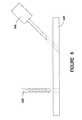
- FIG. 6is diagram of a drill and a laser for perforating a substrate.
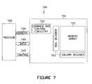
- FIG. 7is a block diagram of a computer system in which embodiments of the present invention can be practiced.
- FIG. 1Ais a cutaway view of some embodiments of inductor 100 of the present invention.
- Inductor 100includes substrate 103 , a plurality of conductive segments 106 , a plurality of conductive segments 109 , and magnetic film layers 112 and 113 .
- the plurality of conductive segments 109interconnect the plurality of conductive segments 106 to form highly conductive path 114 interwoven with substrate 103 .
- Magnetic film layers 112 and 113are formed on substrate 103 in core area 115 of highly conductive path 114 .
- Substrate 103provides the structure in which highly conductive path 114 that constitutes an inductive coil is interwoven.
- Substrate 103in one embodiment, is fabricated from a crystalline material.
- substrate 103is fabricated from a single element doped or undoped semiconductor material, such as silicon or germanium.
- substrate 103is fabricated from gallium arsenide, silicon carbide, or a partially magnetic material having a crystalline or amorphous structure.
- Substrate 103is not limited to a single layer substrate. Multiple layer substrates, coated or partially coated substrates, and substrates having a plurality of coated surfaces are all suitable for use in connection with the present invention.
- the coatingsinclude insulators, ferromagnetic materials, and magnetic oxides.
- Insulatorsprotect the inductive coil and separate the electrically conductive inductive coil from other conductors, such as signal carrying circuit lines. Coatings and films of ferromagnetic materials, such as magnetic metals, alloys, and oxides, increase the inductance of the inductive coil.
- Substrate 103has a plurality of surfaces 118 .
- the plurality of surfaces 118is not limited to oblique surfaces. In one embodiment, at least two of the plurality of surfaces 118 are parallel. In an alternate embodiment, a first pair of parallel surfaces are substantially perpendicular to a second pair of surfaces. In still another embodiment, the surfaces are planarized. Since most integrated circuit manufacturing processes are designed to work with substrates having a pair of relatively flat or planarized parallel surfaces, the use of parallel surfaces simplifies the manufacturing process for forming highly conductive path 114 of inductor 100 .
- Substrate 103has a plurality of holes, perforations, or other substrate subtending paths 121 that can be filled, plugged, partially filed, partially plugged, or lined with a conducting material.
- substrate subtending paths 121are filled by the plurality of conducting segments 106 .
- the shape of the perforations, holes, or other substrate subtending paths 121is not limited to a particular shape. Circular, square, rectangular, and triangular shapes are all suitable for use in connection with the present invention.
- the plurality of holes, perforations, or other substrate subtending paths 121in one embodiment, are substantially parallel to each other and substantially perpendicular to substantially parallel surfaces of the substrate.
- Highly conductive path 114is interwoven with a single layer substrate or a multilayer substrate, such as substrate 103 in combination with magnetic film layers 112 and 113 , to form an inductive element that is at least partially embedded in the substrate. If the surface of the substrate is coated, for example with magnetic film 112 , then conductive path 114 is located at least partially above the coating, pierces the coated substrate, and is interlaced with the coated substrate.
- Highly conductive path 114has an inductance value and is in the shape of a coil.
- the shape of each loop of the coil interlaced with the substrateis not limited to a particular geometric shape. For example, circular, square, rectangular, and triangular loops are suitable for use in connection with the present invention.
- Highly conductive path 114in one embodiment, intersects a plurality of substantially parallel surfaces and fills a plurality of substantially parallel holes.
- Highly conductive path 114is formed from a plurality of interconnected conductive segments.
- the conductive segmentsin one embodiment, are a pair of substantially parallel rows of conductive columns interconnected by a plurality of conductive segments to form a plurality of loops.
- Highly conductive path 114in one embodiment, is fabricated from a metal conductor, such as aluminum, copper, or gold or an alloy of a such a metal conductor.
- a metal conductorsuch as aluminum, copper, or gold or an alloy of a such a metal conductor.
- Aluminum, copper, or gold, or an alloyis used to fill or partially fill the holes, perforations, or other paths subtending the substrate to form a plurality of conductive segments.
- a conductive materialmay be used to plug the holes, perforations, or other paths subtending the substrate to form a plurality of conductive segments. In general, higher conductivity materials are preferred to lower conductivity materials.
- conductive path 114is partially diffused into the substrate or partially diffused into the crystalline structure.
- each segmentin one embodiment, is fabricated from a different conductive material.
- An advantage of interconnecting segments fabricated from different conductive materials to form a conductive pathis that the properties of the conductive path are easily tuned through the choice of the conductive materials. For example, the internal resistance of a conductive path is increased by selecting a material having a higher resistance for a segment than the average resistance in the rest of the path.
- two different conductive materialsare selected for fabricating a conductive path. In this embodiment, materials are selected based on their compatibility with the available integrated circuit manufacturing processes.
- the conductive segments that pierce the substrateare fabricated from aluminum.
- copperis used for these segments.
- Highly conductive path 114is comprised of two types of conductive segments.
- the first typeincludes segments subtending the substrate, such as conductive segments 106 .
- the second typeincludes segments formed on a surface of the substrate, such as conductive segments 109 .
- the second type of segmentinterconnects segments of the first type to form highly conductive path 114 .
- the mid-segment cross-sectional profile 124 of the first type of segmentis not limited to a particular shape. Circular, square, rectangular, and triangular are all shapes suitable for use in connection with the present invention.
- the mid-segment cross-sectional profile 127 of the second type of segmentis not limited to a particular shape. In one embodiment, the mid-segment cross-sectional profile is rectangular.
- the coil that results from forming the highly conductive path from the conductive segments and interweaving the highly conductive path with the substrateis capable of producing a reinforcing magnetic field or flux in the substrate material occupying the core area of the coil and in any coating deposited on the surfaces of the substrate.
- FIG. 1Bis a top view of FIG. 1A with magnetic film 112 formed on substrate 103 between conductive segments 109 and the surface of substrate 103 .
- Magnetic film 112coats or partially coats the surface of substrate 103 .
- magnetic film 112is a magnetic oxide.
- magnetic film 112is one or more layers of a magnetic material in a plurality of layers formed on the surface of substrate 103 .
- Magnetic film 112is formed on substrate 103 to increase the inductance of highly conductive path 114 .
- Methods of preparing magnetic film 112include evaporation, sputtering, chemical vapor deposition, laser ablation, and electrochemical deposition.
- high coercivity gamma iron oxide filmsare deposited using chemical vapor pyrolysis. When deposited at above 500 degrees centigrade these films are magnetic gamma oxide.
- amorphous iron oxide filmsare prepared by the deposition of iron metal in an oxygen atmosphere (10 ⁇ 4 torr) by evaporation.
- an iron-oxide filmis prepared by reactive sputtering of an Fe target in Ar+O 2 atmosphere at a deposition rate of ten times higher than the conventional method.
- the resulting alpha iron oxide filmsare then converted to magnetic gamma type by reducing them in a hydrogen atmosphere.
- FIG. 1Cis a side view of some embodiments of the inductor of FIG. 1A including substrate 103 , the plurality of conductive segments 106 , the plurality of conductive segments 109 and magnetic films 112 and 113 .
- FIG. 2is a cross-sectional side view of some embodiments of highly conductive path 203 including encapsulated magnetic material layers 206 and 209 .
- Encapsulated magnetic material layers 206 and 209are a nickel iron alloy deposited on a surface of substrate 212 .
- Formed on magnetic material layer layers 206 and 209are insulating layers 215 and 218 and second insulating layers 221 and 224 which encapsulate highly conductive path 203 deposited on insulating layers 215 and 218 .
- Insulating layers 215 , 218 , 221 and 224in one embodiment are formed from an insulator, such as polyimide.
- insulating layers 215 , 218 , 221 , and 224are an inorganic oxide, such as silicon dioxide or silicon nitride. The insulator may also partially line the holes, perforations, or other substrate subtending paths.
- the purpose of insulating layers 215 and 218which in one embodiment are dielectrics, is to electrically isolate the surface conducting segments of highly conductive path 203 from magnetic material layers 206 and 209 .
- the purpose of insulating layers 221 and 224is to electrically isolate the highly conductive path 203 from any conducting layers deposited above the path 203 and to protect the path 203 from physical damage.
- the field created by the conductive pathis substantially parallel to the planarized surface and penetrates the coating.
- the conductive pathis operable for creating a magnetic field within the coating, but not above the coating.
- the conductive pathis operable for creating a reinforcing magnetic field within the film and within the substrate.
- FIG. 3 A and FIG. 3Bare perspective views of some embodiments of inductor 301 and sense inductors 304 and 307 of the present invention.
- sense inductor 304is a spiral coil and sense inductor 307 is a test inductor or sense coil embedded in the substrate.
- Sense inductors 304 and 307are capable of detecting and measuring reinforcing magnetic field or flux 309 generated by inductor 301 , and of assisting in the calibration of inductor 301 .
- sense inductor 304is fabricated on one of the surfaces substantially perpendicular to the surfaces of the substrate having the conducting segments, so magnetic field or flux 309 generated by inductor 301 is substantially perpendicular to sense inductor 304 .
- Detachable test leads 310 and 313 in FIG. 3 A and detachable test leads 316 and 319 in FIG. 3Bare capable of coupling sense inductors 304 and 307 to sense or measurement circuits. When coupled to sense or measurement circuits, sense inductors 304 and 307 are decoupled from the sense or measurement circuits by severing test leads 310 , 313 , 316 , and 319 . In one embodiment, test leads 310 , 313 , 316 , and 316 are severed using a laser.
- a currentflows in inductor 301 and generates magnetic field or flux 309 .
- Magnetic field or flux 309passes through sense inductor 304 or sense inductor 307 and induces a current in spiral sense inductor 304 or sense inductor 307 .
- the induced currentcan be detected, measured and used to deduce the inductance of inductor 301 .
- FIG. 4is a cutaway perspective view of some embodiments of triangular coil inductor 400 of the present invention.
- Triangular coil inductor 400comprises substrate 403 and triangular coil 406 .
- An advantage of triangular coil inductor 400is that it saves at least a process step over the previously described coil inductor.
- Triangular coil inductor 400only requires the construction of three segments for each coil of inductor 400 , where the previously described inductor required the construction of four segments for each coil of the inductor.
- FIG. 5is a top view of some embodiments of an inductor coupled circuit 500 of the present invention.
- Inductor coupled circuit 500comprises substrate 503 , coating 506 , coil 509 , and circuit or memory cells 512 .
- Coil 509comprises a conductive path located at least partially above coating 506 and coupled to circuit or memory cells 512 .
- Coil 509pierces substrate 503 , is interlaced with substrate 503 , and produces a magnetic field in coating 506 .
- coil 509produces a magnetic field in coating 506 , but not above coating 506 .
- substrate 503is perforated with a plurality of substantially parallel perforations and is partially magnetic.
- substrate 503is a substrate as described above in connection with FIG. 1 .
- coating 506is a magnetic film as described above in connection with FIG. 1 .
- coil 509is a highly conductive path as described in connection with FIG. 1 .
- FIG. 6is a diagram of a drill 603 and a laser 606 for perforating a substrate 609 .
- Substrate 609has holes, perforations, or other substrate 609 subtending paths.
- a diamond tipped carbide drillis used bore holes or create perforations in substrate 609 .
- laser 606is used to bore a plurality of holes in substrate 609 .
- holes, perforations, or other substrate 609 subtending pathsare fabricated using a dry etching process.
- FIG. 7is a block diagram of a system level embodiment of the present invention.
- System 700comprises processor 705 and memory device 710 , which includes memory circuits and cells, electronic circuits, electronic devices, and power supply circuits coupled to inductors of one or more of the types described above in conjunction with FIGS. 1A-5.
- Memory device 710comprises memory array 715 , address circuitry 720 , and read circuitry 730 , and is coupled to processor 705 by address bus 735 , data bus 740 , and control bus 745 .
- Processor 705through address bus 735 , data bus 740 , and control bus 745 communicates with memory device 710 .
- address information, data information, and control informationare provided to memory device 710 through busses 735 , 740 , and 745 .
- This informationis decoded by addressing circuitry 720 , including a row decoder and a column decoder, and read circuitry 730 .
- Successful completion of the read operationresults in information from memory array 715 being communicated to processor 705 over data bus 740 .
- Embodiments of inductors and methods of fabricating inductors suitable for use with integrated circuitshave been described.
- an inductor having a highly conductive path fabricated from a plurality of conductive segments, and including coatings and films of ferromagnetic materials, such as magnetic metals, alloys, and oxideshas been described.
- an inductor capable of being fabricated from a plurality of conductors having different resistanceshas been described.
- an integrated test or calibration coilcapable of being fabricated on the same substrate as an inductor and capable of facilitating the measurement of the magnetic field or flux generated by the inductor and capable of facilitating the calibration the inductor has been described.
Landscapes
- Engineering & Computer Science (AREA)
- Power Engineering (AREA)
- Microelectronics & Electronic Packaging (AREA)
- Semiconductor Integrated Circuits (AREA)
- Coils Or Transformers For Communication (AREA)
Abstract
Description
Claims (38)
Priority Applications (1)
| Application Number | Priority Date | Filing Date | Title |
|---|---|---|---|
| US10/102,070US6701607B2 (en) | 1999-07-09 | 2002-03-19 | Integrated circuit inductors |
Applications Claiming Priority (3)
| Application Number | Priority Date | Filing Date | Title |
|---|---|---|---|
| US09/350,601US6240622B1 (en) | 1999-07-09 | 1999-07-09 | Integrated circuit inductors |
| US09/821,240US6357107B2 (en) | 1999-07-09 | 2001-03-29 | Integrated circuit inductors |
| US10/102,070US6701607B2 (en) | 1999-07-09 | 2002-03-19 | Integrated circuit inductors |
Related Parent Applications (1)
| Application Number | Title | Priority Date | Filing Date |
|---|---|---|---|
| US09/821,240DivisionUS6357107B2 (en) | 1999-07-09 | 2001-03-29 | Integrated circuit inductors |
Publications (2)
| Publication Number | Publication Date |
|---|---|
| US20020095777A1 US20020095777A1 (en) | 2002-07-25 |
| US6701607B2true US6701607B2 (en) | 2004-03-09 |
Family
ID=23377426
Family Applications (20)
| Application Number | Title | Priority Date | Filing Date |
|---|---|---|---|
| US09/350,601Expired - LifetimeUS6240622B1 (en) | 1999-07-09 | 1999-07-09 | Integrated circuit inductors |
| US09/821,240Expired - LifetimeUS6357107B2 (en) | 1999-07-09 | 2001-03-29 | Integrated circuit inductors |
| US09/850,573Expired - LifetimeUS6762478B2 (en) | 1999-07-09 | 2001-05-07 | Integrated circuit inductors |
| US09/871,454Expired - LifetimeUS6612019B2 (en) | 1999-07-09 | 2001-05-31 | Integrated circuit inductors |
| US09/871,062Expired - LifetimeUS6446327B2 (en) | 1999-07-09 | 2001-05-31 | Integrated circuit inductors |
| US10/100,720Expired - LifetimeUS7158004B2 (en) | 1999-07-09 | 2002-03-18 | Integrated circuit inductors |
| US10/100,710Expired - LifetimeUS6825747B2 (en) | 1999-07-09 | 2002-03-18 | Integrated circuit inductors |
| US10/101,403Expired - LifetimeUS6850141B2 (en) | 1999-07-09 | 2002-03-18 | Integrated circuit inductors |
| US10/100,715Expired - LifetimeUS6910260B2 (en) | 1999-07-09 | 2002-03-18 | Integrated circuit inductors |
| US10/101,142Expired - LifetimeUS6900716B2 (en) | 1999-07-09 | 2002-03-18 | Integrated circuit inductors |
| US10/100,709Expired - LifetimeUS7388462B2 (en) | 1999-07-09 | 2002-03-18 | Integrated circuit inductors |
| US10/101,419Expired - LifetimeUS6646534B2 (en) | 1999-07-09 | 2002-03-18 | Integrated circuit inductors |
| US10/100,702Expired - LifetimeUS6976300B2 (en) | 1999-07-09 | 2002-03-18 | Integrated circuit inductors |
| US10/100,706Expired - LifetimeUS6817087B2 (en) | 1999-07-09 | 2002-03-18 | Integrated circuit inductors |
| US10/101,404Expired - LifetimeUS6822545B2 (en) | 1999-07-09 | 2002-03-18 | Integrated circuit inductors |
| US10/102,071Expired - LifetimeUS6760967B2 (en) | 1999-07-09 | 2002-03-19 | Integrated circuit inductors |
| US10/100,789Expired - LifetimeUS6779250B2 (en) | 1999-07-09 | 2002-03-19 | Integrated circuit inductors |
| US10/102,420Expired - LifetimeUS6948230B2 (en) | 1999-07-09 | 2002-03-19 | Integrated circuit inductors |
| US10/102,070Expired - LifetimeUS6701607B2 (en) | 1999-07-09 | 2002-03-19 | Integrated circuit inductors |
| US11/023,713AbandonedUS20050122199A1 (en) | 1999-07-09 | 2004-12-28 | Integrated circuit inductors |
Family Applications Before (18)
| Application Number | Title | Priority Date | Filing Date |
|---|---|---|---|
| US09/350,601Expired - LifetimeUS6240622B1 (en) | 1999-07-09 | 1999-07-09 | Integrated circuit inductors |
| US09/821,240Expired - LifetimeUS6357107B2 (en) | 1999-07-09 | 2001-03-29 | Integrated circuit inductors |
| US09/850,573Expired - LifetimeUS6762478B2 (en) | 1999-07-09 | 2001-05-07 | Integrated circuit inductors |
| US09/871,454Expired - LifetimeUS6612019B2 (en) | 1999-07-09 | 2001-05-31 | Integrated circuit inductors |
| US09/871,062Expired - LifetimeUS6446327B2 (en) | 1999-07-09 | 2001-05-31 | Integrated circuit inductors |
| US10/100,720Expired - LifetimeUS7158004B2 (en) | 1999-07-09 | 2002-03-18 | Integrated circuit inductors |
| US10/100,710Expired - LifetimeUS6825747B2 (en) | 1999-07-09 | 2002-03-18 | Integrated circuit inductors |
| US10/101,403Expired - LifetimeUS6850141B2 (en) | 1999-07-09 | 2002-03-18 | Integrated circuit inductors |
| US10/100,715Expired - LifetimeUS6910260B2 (en) | 1999-07-09 | 2002-03-18 | Integrated circuit inductors |
| US10/101,142Expired - LifetimeUS6900716B2 (en) | 1999-07-09 | 2002-03-18 | Integrated circuit inductors |
| US10/100,709Expired - LifetimeUS7388462B2 (en) | 1999-07-09 | 2002-03-18 | Integrated circuit inductors |
| US10/101,419Expired - LifetimeUS6646534B2 (en) | 1999-07-09 | 2002-03-18 | Integrated circuit inductors |
| US10/100,702Expired - LifetimeUS6976300B2 (en) | 1999-07-09 | 2002-03-18 | Integrated circuit inductors |
| US10/100,706Expired - LifetimeUS6817087B2 (en) | 1999-07-09 | 2002-03-18 | Integrated circuit inductors |
| US10/101,404Expired - LifetimeUS6822545B2 (en) | 1999-07-09 | 2002-03-18 | Integrated circuit inductors |
| US10/102,071Expired - LifetimeUS6760967B2 (en) | 1999-07-09 | 2002-03-19 | Integrated circuit inductors |
| US10/100,789Expired - LifetimeUS6779250B2 (en) | 1999-07-09 | 2002-03-19 | Integrated circuit inductors |
| US10/102,420Expired - LifetimeUS6948230B2 (en) | 1999-07-09 | 2002-03-19 | Integrated circuit inductors |
Family Applications After (1)
| Application Number | Title | Priority Date | Filing Date |
|---|---|---|---|
| US11/023,713AbandonedUS20050122199A1 (en) | 1999-07-09 | 2004-12-28 | Integrated circuit inductors |
Country Status (1)
| Country | Link |
|---|---|
| US (20) | US6240622B1 (en) |
Cited By (3)
| Publication number | Priority date | Publication date | Assignee | Title |
|---|---|---|---|---|
| US20020095776A1 (en)* | 1999-07-09 | 2002-07-25 | Micron Technology, Inc. | Integrated circuit inductors |
| US20090283854A1 (en)* | 2008-05-19 | 2009-11-19 | Levy Max G | Design Structure and Method for Buried Inductors for Ultra-High Resistivity Wafers for SOI/RF SIGE Applications |
| US8232173B2 (en) | 2010-11-01 | 2012-07-31 | International Business Machines Corporation | Structure and design structure for high-Q value inductor and method of manufacturing the same |
Families Citing this family (110)
| Publication number | Priority date | Publication date | Assignee | Title |
|---|---|---|---|---|
| US6286062B1 (en) | 1997-07-01 | 2001-09-04 | Micron Technology, Inc. | Pipelined packet-oriented memory system having a unidirectional command and address bus and a bidirectional data bus |
| US7107666B2 (en)* | 1998-07-23 | 2006-09-19 | Bh Electronics | Method of manufacturing an ultra-miniature magnetic device |
| JP2002324714A (en)* | 2001-02-21 | 2002-11-08 | Tdk Corp | Coil sealed dust core and its manufacturing method |
| US6639298B2 (en) | 2001-06-28 | 2003-10-28 | Agere Systems Inc. | Multi-layer inductor formed in a semiconductor substrate |
| US6667536B2 (en) | 2001-06-28 | 2003-12-23 | Agere Systems Inc. | Thin film multi-layer high Q transformer formed in a semiconductor substrate |
| US6802949B2 (en)* | 2001-10-15 | 2004-10-12 | Hanyang Hak Won Co., Ltd. | Method for manufacturing half-metallic magnetic oxide and plasma sputtering apparatus used in the same |
| US6635948B2 (en)* | 2001-12-05 | 2003-10-21 | Micron Technology, Inc. | Semiconductor device with electrically coupled spiral inductors |
| US6614093B2 (en)* | 2001-12-11 | 2003-09-02 | Lsi Logic Corporation | Integrated inductor in semiconductor manufacturing |
| US6856003B2 (en)* | 2002-09-05 | 2005-02-15 | Industrial Technology Research Institute | Microelectronic 3-D solenoid of circular cross-section and method for fabrication |
| JP3800540B2 (en)* | 2003-01-31 | 2006-07-26 | Tdk株式会社 | Inductance element manufacturing method, multilayer electronic component, multilayer electronic component module, and manufacturing method thereof |
| TWI226647B (en)* | 2003-06-11 | 2005-01-11 | Via Tech Inc | Inductor formed between two layout layers |
| US7229908B1 (en) | 2004-06-04 | 2007-06-12 | National Semiconductor Corporation | System and method for manufacturing an out of plane integrated circuit inductor |
| KR100548388B1 (en)* | 2004-07-20 | 2006-02-02 | 삼성전자주식회사 | Low Loss Inductor Device and Manufacturing Method Thereof |
| DE102005014929B4 (en)* | 2005-04-01 | 2008-04-17 | Newlogic Technologies Gmbh | Integrated coil and integrated transformer |
| US7410894B2 (en)* | 2005-07-27 | 2008-08-12 | International Business Machines Corporation | Post last wiring level inductor using patterned plate process |
| DE602005020005D1 (en)* | 2005-09-09 | 2010-04-29 | St Microelectronics Srl | Inductive arrangement |
| US9754712B2 (en) | 2005-09-22 | 2017-09-05 | Radial Electronics, Inc. | Embedded magnetic components and methods |
| WO2011014200A1 (en) | 2009-07-31 | 2011-02-03 | Radial Electronics, Inc | Embedded magnetic components and methods |
| US7477128B2 (en) | 2005-09-22 | 2009-01-13 | Radial Electronics, Inc. | Magnetic components |
| US10049803B2 (en) | 2005-09-22 | 2018-08-14 | Radial Electronics, Inc. | Arrayed embedded magnetic components and methods |
| US10431367B2 (en) | 2005-09-22 | 2019-10-01 | Radial Electronics, Inc. | Method for gapping an embedded magnetic device |
| US10522279B2 (en) | 2005-09-22 | 2019-12-31 | Radial Electronics, Inc. | Embedded high voltage transformer components and methods |
| US7187179B1 (en) | 2005-10-19 | 2007-03-06 | International Business Machines Corporation | Wiring test structures for determining open and short circuits in semiconductor devices |
| KR100723032B1 (en)* | 2005-10-19 | 2007-05-30 | 삼성전자주식회사 | High efficiency inductor, manufacturing method of inductor and packaging structure using inductor |
| JP2007266105A (en)* | 2006-03-27 | 2007-10-11 | Tdk Corp | Thin-film device |
| US7843302B2 (en)* | 2006-05-08 | 2010-11-30 | Ibiden Co., Ltd. | Inductor and electric power supply using it |
| US7636242B2 (en)* | 2006-06-29 | 2009-12-22 | Intel Corporation | Integrated inductor |
| US8378777B2 (en)* | 2008-07-29 | 2013-02-19 | Cooper Technologies Company | Magnetic electrical device |
| US9216850B2 (en) | 2006-09-26 | 2015-12-22 | Intercontinental Great Brands Llc | Rupturable substrate |
| US9169052B2 (en)* | 2006-09-26 | 2015-10-27 | Intercontinental Great Brands Llc | Rupturable blister package |
| US7622910B2 (en)* | 2006-10-06 | 2009-11-24 | Honeywell International Inc. | Method and apparatus for AC integrated current sensor |
| EP2082468A2 (en)* | 2006-10-26 | 2009-07-29 | Koninklijke Philips Electronics N.V. | Floor covering and inductive power system |
| TWI303957B (en)* | 2006-12-11 | 2008-12-01 | Ind Tech Res Inst | Embedded inductor devices and fabrication methods thereof |
| TWI338549B (en)* | 2007-01-03 | 2011-03-01 | Advanced Semiconductor Eng | Via hole structure and manufacturing method thereof |
| JP2008171965A (en)* | 2007-01-11 | 2008-07-24 | Fuji Electric Device Technology Co Ltd | Ultra-compact power converter |
| TWI347616B (en)* | 2007-03-22 | 2011-08-21 | Ind Tech Res Inst | Inductor devices |
| WO2008152641A2 (en)* | 2007-06-12 | 2008-12-18 | Advanced Magnetic Solutions Ltd. | Magnetic induction devices and methods for producing them |
| US20090085704A1 (en) | 2007-10-01 | 2009-04-02 | Infineon Technologies Austria Ag | Chip inductor |
| US7884696B2 (en)* | 2007-11-23 | 2011-02-08 | Alpha And Omega Semiconductor Incorporated | Lead frame-based discrete power inductor |
| US7741133B2 (en)* | 2007-12-17 | 2010-06-22 | Hitachi Global Storage Technologies Netherlands, B.V. | Resistance measurements of a helical coil |
| US8058707B1 (en)* | 2008-03-03 | 2011-11-15 | Xilinx, Inc. | Semiconductor devices having redundant through-die vias and methods of fabricating the same |
| US20090309687A1 (en) | 2008-06-11 | 2009-12-17 | Aleksandar Aleksov | Method of manufacturing an inductor for a microelectronic device, method of manufacturing a substrate containing such an inductor, and substrate manufactured thereby, |
| WO2010031055A1 (en)* | 2008-09-15 | 2010-03-18 | Newlife Sciences Llc | Spherical vibrating probe apparatus and method for conducting efficacy analysis of pain treatment using probe apparatus |
| JP5536656B2 (en)* | 2008-09-18 | 2014-07-02 | ルネサスエレクトロニクス株式会社 | Semiconductor device |
| WO2010064412A1 (en)* | 2008-12-04 | 2010-06-10 | 日本電気株式会社 | Bias circuit and method for making bias circuit |
| US9721715B2 (en)* | 2009-01-22 | 2017-08-01 | 2Sentient Inc. | Solid state components having an air core |
| FR2944354B1 (en)* | 2009-04-10 | 2011-06-24 | Commissariat Energie Atomique | DEVICE FOR NON-DESTRUCTIVE CONTROL OF AN ELECTRICALLY CONDUCTIVE STRUCTURE |
| TWM366158U (en)* | 2009-04-14 | 2009-10-01 | Domintech Co Ltd | Miniature inductance |
| JP2010267643A (en)* | 2009-05-12 | 2010-11-25 | Toshiba Corp | Semiconductor device |
| US8697574B2 (en)* | 2009-09-25 | 2014-04-15 | Infineon Technologies Ag | Through substrate features in semiconductor substrates |
| US8451921B2 (en)* | 2009-10-28 | 2013-05-28 | Qualcomm Incorporated | Method and an apparatus for adaptively learning a sparse impulse response of a continuous channel |
| US8068003B2 (en)* | 2010-03-10 | 2011-11-29 | Altera Corporation | Integrated circuits with series-connected inductors |
| US8384507B2 (en)* | 2010-06-01 | 2013-02-26 | Qualcomm Incorporated | Through via inductor or transformer in a high-resistance substrate with programmability |
| CA2819461A1 (en) | 2010-11-30 | 2012-06-07 | Newlife Sciences Llc | Apparatus and method for treatment of pain with body impedance analyzer |
| CN102569249B (en)* | 2010-12-08 | 2014-01-22 | 财团法人工业技术研究院 | Three-dimensional inductor |
| US8405482B2 (en) | 2011-02-23 | 2013-03-26 | Taiwan Semiconductor Manufacturing Company, Ltd. | Integrated circuits including inductors |
| KR20130001984A (en)* | 2011-06-28 | 2013-01-07 | 삼성전기주식회사 | Gap composition of multi layered power inductor and multi layered power inductor comprising gap layer using the same |
| US8354325B1 (en) | 2011-06-29 | 2013-01-15 | Freescale Semiconductor, Inc. | Method for forming a toroidal inductor in a semiconductor substrate |
| US9105627B2 (en) | 2011-11-04 | 2015-08-11 | International Business Machines Corporation | Coil inductor for on-chip or on-chip stack |
| US9673268B2 (en) | 2011-12-29 | 2017-06-06 | Intel Corporation | Integrated inductor for integrated circuit devices |
| TWI442422B (en)* | 2012-01-19 | 2014-06-21 | Ind Tech Res Inst | Inductor structure |
| US9257221B2 (en)* | 2012-04-13 | 2016-02-09 | Cyntec Co., Ltd. | Through-hole via inductor in a high-frequency device |
| US9111933B2 (en) | 2012-05-17 | 2015-08-18 | International Business Machines Corporation | Stacked through-silicon via (TSV) transformer structure |
| DE102012216101B4 (en)* | 2012-09-12 | 2016-03-24 | Festo Ag & Co. Kg | Method for producing a coil integrated in a substrate, method for producing a multilayer printed circuit board and electronic device |
| US9343442B2 (en) | 2012-09-20 | 2016-05-17 | Taiwan Semiconductor Manufacturing Company, Ltd. | Passive devices in package-on-package structures and methods for forming the same |
| KR20130010915A (en)* | 2012-10-23 | 2013-01-29 | 김성동 | Three-dimensional semiconductor devices having a cache memory array, in which chapter data can be stored, and methods of operating the same |
| DE102012220022B4 (en)* | 2012-11-02 | 2014-09-25 | Festo Ag & Co. Kg | Method of manufacturing a coil and electronic device |
| CN103824840B (en)* | 2012-11-16 | 2017-03-15 | 南京理工大学 | Solenoid type differential inductance based on silicon hole |
| US9705478B2 (en) | 2013-08-01 | 2017-07-11 | Qorvo Us, Inc. | Weakly coupled tunable RF receiver architecture |
| US9196406B2 (en)* | 2013-03-15 | 2015-11-24 | Rf Micro Devices, Inc. | High Q factor inductor structure |
| US9391565B2 (en) | 2013-03-15 | 2016-07-12 | TriQuint International PTE, Ltd. | Amplifier phase distortion correction based on amplitude distortion measurement |
| US9899133B2 (en) | 2013-08-01 | 2018-02-20 | Qorvo Us, Inc. | Advanced 3D inductor structures with confined magnetic field |
| US12224096B2 (en) | 2013-03-15 | 2025-02-11 | Qorvo Us, Inc. | Advanced 3D inductor structures with confined magnetic field |
| US9502168B1 (en) | 2013-11-15 | 2016-11-22 | Altera Corporation | Interleaved T-coil structure and a method of manufacturing the T-coil structure |
| JP2015188051A (en)* | 2014-03-14 | 2015-10-29 | 株式会社東芝 | Photocoupler |
| WO2015190229A1 (en)* | 2014-06-11 | 2015-12-17 | 株式会社村田製作所 | Coil component |
| US9275786B2 (en)* | 2014-07-18 | 2016-03-01 | Qualcomm Incorporated | Superposed structure 3D orthogonal through substrate inductor |
| US9704739B2 (en) | 2014-07-30 | 2017-07-11 | Taiwan Semiconductor Manufacturing Company, Ltd. | Semiconductor device packages, packaging methods, and packaged semiconductor devices |
| US9824811B2 (en) | 2014-12-19 | 2017-11-21 | Texas Instruments Incorporated | Embedded coil assembly and method of making |
| KR101642643B1 (en)* | 2015-01-27 | 2016-07-29 | 삼성전기주식회사 | Coil component and method of manufacturing the same |
| US10878997B2 (en) | 2015-03-13 | 2020-12-29 | Taiwan Semiconductor Manufacturing Company, Ltd. | Integrated circuit having current-sensing coil |
| KR101681409B1 (en)* | 2015-04-16 | 2016-12-12 | 삼성전기주식회사 | Coil electronic component |
| US10290414B2 (en) | 2015-08-31 | 2019-05-14 | Qualcomm Incorporated | Substrate comprising an embedded inductor and a thin film magnetic core |
| US20170062398A1 (en)* | 2015-09-02 | 2017-03-02 | Qualcomm Incorporated | Integration of inductors with advanced-node system-on-chip (soc) using glass wafer with inductors and wafer-to-wafer joining |
| US9959964B2 (en)* | 2015-11-13 | 2018-05-01 | Qualcomm Incorporated | Thin film magnet inductor structure for high quality (Q)-factor radio frequency (RF) applications |
| US9954267B2 (en)* | 2015-12-28 | 2018-04-24 | Qualcomm Incorporated | Multiplexer design using a 2D passive on glass filter integrated with a 3D through glass via filter |
| WO2017124200A2 (en)* | 2016-01-20 | 2017-07-27 | Jaquet Technology Group Ag | Manufacturing method for a sensing element and sensor device |
| WO2017134993A1 (en)* | 2016-02-02 | 2017-08-10 | 株式会社村田製作所 | Surface mount type coil component, method of manufacturing same, and dc-dc converter using same |
| US11139238B2 (en) | 2016-12-07 | 2021-10-05 | Qorvo Us, Inc. | High Q factor inductor structure |
| US20180197676A1 (en)* | 2017-01-10 | 2018-07-12 | General Electric Company | Insulation for tranformer or inductor |
| KR101952866B1 (en)* | 2017-02-22 | 2019-02-27 | 삼성전기주식회사 | Power inductor, board having the same, and current measurement method using the same |
| US10553354B2 (en) | 2017-03-10 | 2020-02-04 | International Business Machines Corporation | Method of manufacturing inductor with ferromagnetic cores |
| EP3750174B1 (en) | 2018-02-11 | 2023-07-19 | Danmarks Tekniske Universitet | Semiconductor substrate member |
| US11404201B2 (en) | 2018-03-26 | 2022-08-02 | Tesla, Inc. | Method of manufacturing inductors |
| DE102018117349B4 (en)* | 2018-07-18 | 2020-07-16 | B-Horizon GmbH | Device for measuring pressure and humidity |
| US10972001B2 (en) | 2018-08-13 | 2021-04-06 | Intel Corporation | Multi-terminal inductors for voltage regulators |
| US20200312795A1 (en)* | 2019-03-29 | 2020-10-01 | Silego Technology Inc. | Packaging Substrate |
| IL288836B2 (en) | 2019-06-12 | 2024-01-01 | Truerelief Llc | System and method for delivering pulsed electric current to living tissue |
| EP3840547A1 (en)* | 2019-12-20 | 2021-06-23 | AT & S Austria Technologie & Systemtechnik Aktiengesellschaft | Component carrier with embedded magnetic inlay and integrated coil structure |
| CN111309197B (en)* | 2020-01-19 | 2024-08-16 | 深圳市鸿合创新信息技术有限责任公司 | Sensing film and manufacturing method thereof, sensing plate and manufacturing method thereof, and display device |
| US11911605B2 (en) | 2021-03-05 | 2024-02-27 | Truerelief Llc | Method and apparatus for injury treatment |
| EP4095534B1 (en) | 2021-05-27 | 2024-07-17 | Hitachi Energy Ltd | Semiconductor assembly, electric power device and method of manufacturing |
| US20220408562A1 (en)* | 2021-06-16 | 2022-12-22 | Intel Corporation | Integrated rf passive devices on glass |
| WO2023090438A1 (en)* | 2021-11-18 | 2023-05-25 | ソマール株式会社 | Magnetic viscous fluid and mechanical device |
| US11749455B2 (en) | 2022-01-10 | 2023-09-05 | Bh Electronics, Inc. | Methods of fabricating ultra-miniature laminated magnetic cores and devices |
| JP2025504140A (en)* | 2022-07-22 | 2025-02-06 | シェンチェン ショックス カンパニー リミテッド | Wearable Devices |
| CN115331927A (en)* | 2022-08-15 | 2022-11-11 | 韩智毅 | Semiconductor structure, preparation method and semiconductor device |
| JPWO2024057707A1 (en)* | 2022-09-12 | 2024-03-21 | ||
| DE102023126454A1 (en)* | 2023-09-28 | 2025-04-03 | Universität Stuttgart, Körperschaft Des Öffentlichen Rechts | Electrical cable, coil and inductive energy transfer device |
| WO2025117982A1 (en)* | 2023-11-30 | 2025-06-05 | Atlas Magnetics Company | Method and apparatus for improving the efficiency of magnetic hybrid cores |
Citations (35)
| Publication number | Priority date | Publication date | Assignee | Title |
|---|---|---|---|---|
| US3553533A (en) | 1964-05-14 | 1971-01-05 | Texas Instruments Inc | Dielectric bodies with selectively formed conductive or metallic portions, composites thereof with semiconductor material and methods of making said bodies and composites |
| US3561110A (en) | 1967-08-31 | 1971-02-09 | Ibm | Method of making connections and conductive paths |
| US3614554A (en) | 1968-10-24 | 1971-10-19 | Texas Instruments Inc | Miniaturized thin film inductors for use in integrated circuits |
| US3731005A (en) | 1971-05-18 | 1973-05-01 | Metalized Ceramics Corp | Laminated coil |
| US3881244A (en) | 1972-06-02 | 1975-05-06 | Texas Instruments Inc | Method of making a solid state inductor |
| US3988764A (en) | 1973-10-30 | 1976-10-26 | General Electric Company | Deep diode solid state inductor coil |
| US3996095A (en) | 1975-04-16 | 1976-12-07 | International Business Machines Corporation | Epitaxial process of forming ferrite, Fe3 O4 and γFe2 O3 thin films on special materials |
| US4024565A (en) | 1973-10-30 | 1977-05-17 | General Electric Company | Deep diode solid state transformer |
| US4729510A (en)* | 1984-11-14 | 1988-03-08 | Itt Corporation | Coaxial shielded helical delay line and process |
| US4839659A (en)* | 1988-08-01 | 1989-06-13 | The United States Of America As Represented By The Secretary Of The Army | Microstrip phase scan antenna array |
| US4845452A (en) | 1987-10-08 | 1989-07-04 | Tdk Corporation | Composite bead element |
| JPH03286512A (en) | 1990-04-03 | 1991-12-17 | Tdk Corp | Manufacture of inductor contained in case |
| US5095357A (en)* | 1989-08-18 | 1992-03-10 | Mitsubishi Denki Kabushiki Kaisha | Inductive structures for semiconductor integrated circuits |
| US5227659A (en) | 1990-06-08 | 1993-07-13 | Trustees Of Boston University | Integrated circuit inductor |
| JPH0689976A (en) | 1992-07-22 | 1994-03-29 | Kawasaki Steel Corp | Semiconductor device |
| JPH06120036A (en) | 1992-10-05 | 1994-04-28 | Fuji Electric Co Ltd | Coil for magnetic induction element |
| US5336921A (en)* | 1992-01-27 | 1994-08-09 | Motorola, Inc. | Vertical trench inductor |
| US5448822A (en) | 1993-03-10 | 1995-09-12 | Quantum Corporation | Method of making a thin film magnetic head having multi-layer coils |
| US5450755A (en) | 1992-10-21 | 1995-09-19 | Matsushita Electric Industrial Co., Ltd. | Mechanical sensor having a U-shaped planar coil and a magnetic layer |
| US5479695A (en) | 1991-05-02 | 1996-01-02 | At&T Corp. | Method of making a multilayer monolithic magnetic component |
| US5696471A (en) | 1995-09-22 | 1997-12-09 | Uniden Corporation | Inductive coupled filter with electrically neutral holes between solid spiral inductors |
| US5767563A (en) | 1995-12-22 | 1998-06-16 | Micron Technology, Inc. | Inductor formed at least partially in a substrate |
| US5801521A (en) | 1990-05-31 | 1998-09-01 | Kabushiki Kaisha Toshiba | Planar magnetic element |
| US5875452A (en) | 1995-12-21 | 1999-02-23 | International Business Machines Corporation | DRAM/SRAM with uniform access time using buffers, write back, address decode, read/write and refresh controllers |
| JPH11251143A (en) | 1998-03-02 | 1999-09-17 | Toshiba Corp | Planar inductor, method of manufacturing the same, and method of forming flat coil pattern |
| US5956073A (en) | 1996-12-19 | 1999-09-21 | Lucent Technologies Inc. | Noise-limiting transformer apparatus and method for making |
| US6013939A (en)* | 1997-10-31 | 2000-01-11 | National Scientific Corp. | Monolithic inductor with magnetic flux lines guided away from substrate |
| US6031273A (en) | 1996-05-02 | 2000-02-29 | Integrated Magnetoelectronics | All-metal, giant magnetoresistive, solid-state component |
| US6069397A (en)* | 1996-05-03 | 2000-05-30 | Motorola, Inc. | Integrable using amorphous magnetic material circuit inductor |
| JP2000269059A (en) | 1999-03-16 | 2000-09-29 | Nippon Telegr & Teleph Corp <Ntt> | Magnetic component and method of manufacturing the same |
| US6240622B1 (en) | 1999-07-09 | 2001-06-05 | Micron Technology, Inc. | Integrated circuit inductors |
| US6249039B1 (en) | 1998-09-10 | 2001-06-19 | Bourns, Inc. | Integrated inductive components and method of fabricating such components |
| US6291872B1 (en)* | 1999-11-04 | 2001-09-18 | Taiwan Semiconductor Manufacturing Co., Ltd. | Three-dimensional type inductor for mixed mode radio frequency device |
| US6303971B1 (en) | 1996-11-19 | 2001-10-16 | Samsung Electronics Co., Ltd. | Inductor for semiconductor device and method for making the same |
| US6542060B2 (en) | 2000-09-12 | 2003-04-01 | Memscap | Microcomponent of the microinductor or microtransformer type |
Family Cites Families (56)
| Publication number | Priority date | Publication date | Assignee | Title |
|---|---|---|---|---|
| US95770A (en)* | 1869-10-12 | Improvement in milking-stocffis | ||
| US3477936A (en)* | 1967-06-29 | 1969-11-11 | Ppg Industries Inc | Sputtering of metals in an atmosphere of fluorine and oxygen |
| US3553553A (en)* | 1969-04-28 | 1971-01-05 | Eaton Yale & Towne | Hoist control system utilizing reversible, variable speed induction motor |
| US3614110A (en)* | 1969-11-13 | 1971-10-19 | Mattel Inc | Voice unit backpack |
| US3659240A (en) | 1970-04-30 | 1972-04-25 | Bourns Inc | Thick-film electric-pulse transformer |
| US3691497A (en) | 1970-10-15 | 1972-09-12 | Us Army | Leadless microminiature inductance element with a closed magnetic circuit |
| US3761005A (en)* | 1972-04-20 | 1973-09-25 | Bell Telephone Labor Inc | Apparatus for aligning and joining tubular members |
| US3731105A (en) | 1972-05-19 | 1973-05-01 | Litton Business Systems Inc | Arc suppressor for dielectric apparatus |
| JPS5971112A (en)* | 1982-10-15 | 1984-04-21 | Comput Basic Mach Technol Res Assoc | thin film magnetic head |
| JPS59232403A (en) | 1983-06-15 | 1984-12-27 | Matsushita Electric Ind Co Ltd | inductor |
| US4560445A (en) | 1984-12-24 | 1985-12-24 | Polyonics Corporation | Continuous process for fabricating metallic patterns on a thin film substrate |
| JPH01125114A (en) | 1987-11-10 | 1989-05-17 | Nec Corp | Semiconductor integrated circuit |
| US4849081A (en)* | 1988-06-22 | 1989-07-18 | The Boc Group, Inc. | Formation of oxide films by reactive sputtering |
| US5047719A (en)* | 1990-05-25 | 1991-09-10 | The Failure Group, Inc. | Flexible coil assembly for reflectance-mode nondestructive eddy-current examination |
| JPH0430308A (en)* | 1990-05-25 | 1992-02-03 | Hitachi Ltd | Magnetic head and its manufacturing method |
| US5192610A (en)* | 1990-06-07 | 1993-03-09 | Applied Materials, Inc. | Corrosion-resistant protective coating on aluminum substrate and method of forming same |
| US5177670A (en) | 1991-02-08 | 1993-01-05 | Hitachi, Ltd. | Capacitor-carrying semiconductor module |
| US5135581A (en)* | 1991-04-08 | 1992-08-04 | Minnesota Mining And Manufacturing Company | Light transmissive electrically conductive oxide electrode formed in the presence of a stabilizing gas |
| JPH0689811A (en)* | 1992-09-07 | 1994-03-29 | Nippon Steel Corp | Thin inductor / transformer and manufacturing method thereof |
| US5430613A (en)* | 1993-06-01 | 1995-07-04 | Eaton Corporation | Current transformer using a laminated toroidal core structure and a lead frame |
| US6728113B1 (en) | 1993-06-24 | 2004-04-27 | Polychip, Inc. | Method and apparatus for non-conductively interconnecting integrated circuits |
| TW262595B (en) | 1993-11-17 | 1995-11-11 | Ikeda Takeshi | |
| US5576680A (en) | 1994-03-01 | 1996-11-19 | Amer-Soi | Structure and fabrication process of inductors on semiconductor chip |
| JPH07272932A (en)* | 1994-03-31 | 1995-10-20 | Canon Inc | Printed inductor |
| US5670415A (en)* | 1994-05-24 | 1997-09-23 | Depositech, Inc. | Method and apparatus for vacuum deposition of highly ionized media in an electromagnetic controlled environment |
| TW265450B (en) | 1994-06-30 | 1995-12-11 | At & T Corp | Devices using metallized magnetic substrates |
| US5534837A (en) | 1994-07-28 | 1996-07-09 | Rockwell International | Orthogonal-field electrically variable magnetic device |
| US5837392A (en)* | 1995-11-30 | 1998-11-17 | Sony Corporation | Soft magnetic thin film and thin film magnetic head using same |
| EP0741395A1 (en) | 1995-05-04 | 1996-11-06 | AT&T IPM Corp. | Post-mountable planar magnetic device and method of manufacture thereof |
| JP4015717B2 (en)* | 1995-06-29 | 2007-11-28 | 日立マクセル株式会社 | Information carrier manufacturing method |
| US5781091A (en)* | 1995-07-24 | 1998-07-14 | Autosplice Systems Inc. | Electronic inductive device and method for manufacturing |
| US5804422A (en) | 1995-09-20 | 1998-09-08 | Shinko Electric Industries Co., Ltd. | Process for producing a semiconductor package |
| JPH09213530A (en)* | 1996-01-30 | 1997-08-15 | Alps Electric Co Ltd | Plane transformer |
| US5969471A (en)* | 1996-02-21 | 1999-10-19 | Industrial Technology Research Institute | Grid assembly for cathode-ray tubes and method of making |
| US6356181B1 (en)* | 1996-03-29 | 2002-03-12 | Murata Manufacturing Co., Ltd. | Laminated common-mode choke coil |
| US5898991A (en)* | 1997-01-16 | 1999-05-04 | International Business Machines Corporation | Methods of fabrication of coaxial vias and magnetic devices |
| US6116863A (en) | 1997-05-30 | 2000-09-12 | University Of Cincinnati | Electromagnetically driven microactuated device and method of making the same |
| US6417754B1 (en) | 1997-12-08 | 2002-07-09 | The Regents Of The University Of California | Three-dimensional coil inductor |
| US20020067570A1 (en)* | 1997-12-12 | 2002-06-06 | Yoshitaka Sasaki | Thin film magnetic head recessed partially into substrate and including plantarization layersi |
| JPH11251147A (en) | 1998-02-27 | 1999-09-17 | Omron Corp | Inductor and transformer using the same |
| US6406988B1 (en) | 1998-04-24 | 2002-06-18 | Amerasia International Technology, Inc. | Method of forming fine pitch interconnections employing magnetic masks |
| US6094123A (en) | 1998-09-25 | 2000-07-25 | Lucent Technologies Inc. | Low profile surface mount chip inductor |
| US6191468B1 (en) | 1999-02-03 | 2001-02-20 | Micron Technology, Inc. | Inductor with magnetic material layers |
| FR2791470B1 (en) | 1999-03-23 | 2001-06-01 | Memscap | MONOLITHIC INTEGRATED CIRCUIT INCORPORATING AN INDUCTIVE COMPONENT AND METHOD FOR MANUFACTURING SUCH AN INTEGRATED CIRCUIT |
| US6346865B1 (en) | 1999-04-29 | 2002-02-12 | Delphi Technologies, Inc. | EMI/RFI filter including a ferroelectric/ferromagnetic composite |
| JP3617426B2 (en)* | 1999-09-16 | 2005-02-02 | 株式会社村田製作所 | Inductor and manufacturing method thereof |
| US6420954B1 (en)* | 1999-12-10 | 2002-07-16 | Micron Technology, Inc. | Coupled multilayer soft magnetic films for high frequency microtransformer for system-on-chip power supply |
| US6531945B1 (en) | 2000-03-10 | 2003-03-11 | Micron Technology, Inc. | Integrated circuit inductor with a magnetic core |
| JP3452028B2 (en)* | 2000-05-09 | 2003-09-29 | 株式会社村田製作所 | Chip inductor and manufacturing method thereof |
| JP4233199B2 (en)* | 2000-06-30 | 2009-03-04 | 富士フイルム株式会社 | Planographic printing plate manufacturing method |
| US6794965B2 (en)* | 2001-01-18 | 2004-09-21 | Arizona State University | Micro-magnetic latching switch with relaxed permanent magnet alignment requirements |
| US6459352B1 (en) | 2001-02-08 | 2002-10-01 | Skyworks Solutions, Inc. | On-chip transformers |
| US6362012B1 (en)* | 2001-03-05 | 2002-03-26 | Taiwan Semiconductor Manufacturing Company | Structure of merged vertical capacitor inside spiral conductor for RF and mixed-signal applications |
| US6573822B2 (en) | 2001-06-18 | 2003-06-03 | Intel Corporation | Tunable inductor using microelectromechanical switches |
| US6636139B2 (en)* | 2001-09-10 | 2003-10-21 | Taiwan Semiconductor Manufacturing Company | Structure to reduce the degradation of the Q value of an inductor caused by via resistance |
| US6614093B2 (en)* | 2001-12-11 | 2003-09-02 | Lsi Logic Corporation | Integrated inductor in semiconductor manufacturing |
- 1999
- 1999-07-09USUS09/350,601patent/US6240622B1/ennot_activeExpired - Lifetime
- 2001
- 2001-03-29USUS09/821,240patent/US6357107B2/ennot_activeExpired - Lifetime
- 2001-05-07USUS09/850,573patent/US6762478B2/ennot_activeExpired - Lifetime
- 2001-05-31USUS09/871,454patent/US6612019B2/ennot_activeExpired - Lifetime
- 2001-05-31USUS09/871,062patent/US6446327B2/ennot_activeExpired - Lifetime
- 2002
- 2002-03-18USUS10/100,720patent/US7158004B2/ennot_activeExpired - Lifetime
- 2002-03-18USUS10/100,710patent/US6825747B2/ennot_activeExpired - Lifetime
- 2002-03-18USUS10/101,403patent/US6850141B2/ennot_activeExpired - Lifetime
- 2002-03-18USUS10/100,715patent/US6910260B2/ennot_activeExpired - Lifetime
- 2002-03-18USUS10/101,142patent/US6900716B2/ennot_activeExpired - Lifetime
- 2002-03-18USUS10/100,709patent/US7388462B2/ennot_activeExpired - Lifetime
- 2002-03-18USUS10/101,419patent/US6646534B2/ennot_activeExpired - Lifetime
- 2002-03-18USUS10/100,702patent/US6976300B2/ennot_activeExpired - Lifetime
- 2002-03-18USUS10/100,706patent/US6817087B2/ennot_activeExpired - Lifetime
- 2002-03-18USUS10/101,404patent/US6822545B2/ennot_activeExpired - Lifetime
- 2002-03-19USUS10/102,071patent/US6760967B2/ennot_activeExpired - Lifetime
- 2002-03-19USUS10/100,789patent/US6779250B2/ennot_activeExpired - Lifetime
- 2002-03-19USUS10/102,420patent/US6948230B2/ennot_activeExpired - Lifetime
- 2002-03-19USUS10/102,070patent/US6701607B2/ennot_activeExpired - Lifetime
- 2004
- 2004-12-28USUS11/023,713patent/US20050122199A1/ennot_activeAbandoned
Patent Citations (36)
| Publication number | Priority date | Publication date | Assignee | Title |
|---|---|---|---|---|
| US3553533A (en) | 1964-05-14 | 1971-01-05 | Texas Instruments Inc | Dielectric bodies with selectively formed conductive or metallic portions, composites thereof with semiconductor material and methods of making said bodies and composites |
| US3561110A (en) | 1967-08-31 | 1971-02-09 | Ibm | Method of making connections and conductive paths |
| US3614554A (en) | 1968-10-24 | 1971-10-19 | Texas Instruments Inc | Miniaturized thin film inductors for use in integrated circuits |
| US3731005A (en) | 1971-05-18 | 1973-05-01 | Metalized Ceramics Corp | Laminated coil |
| US3881244A (en) | 1972-06-02 | 1975-05-06 | Texas Instruments Inc | Method of making a solid state inductor |
| US3988764A (en) | 1973-10-30 | 1976-10-26 | General Electric Company | Deep diode solid state inductor coil |
| US4024565A (en) | 1973-10-30 | 1977-05-17 | General Electric Company | Deep diode solid state transformer |
| US3996095A (en) | 1975-04-16 | 1976-12-07 | International Business Machines Corporation | Epitaxial process of forming ferrite, Fe3 O4 and γFe2 O3 thin films on special materials |
| US4729510A (en)* | 1984-11-14 | 1988-03-08 | Itt Corporation | Coaxial shielded helical delay line and process |
| US4845452A (en) | 1987-10-08 | 1989-07-04 | Tdk Corporation | Composite bead element |
| US4839659A (en)* | 1988-08-01 | 1989-06-13 | The United States Of America As Represented By The Secretary Of The Army | Microstrip phase scan antenna array |
| US5095357A (en)* | 1989-08-18 | 1992-03-10 | Mitsubishi Denki Kabushiki Kaisha | Inductive structures for semiconductor integrated circuits |
| JPH03286512A (en) | 1990-04-03 | 1991-12-17 | Tdk Corp | Manufacture of inductor contained in case |
| US5801521A (en) | 1990-05-31 | 1998-09-01 | Kabushiki Kaisha Toshiba | Planar magnetic element |
| US5227659A (en) | 1990-06-08 | 1993-07-13 | Trustees Of Boston University | Integrated circuit inductor |
| US5479695A (en) | 1991-05-02 | 1996-01-02 | At&T Corp. | Method of making a multilayer monolithic magnetic component |
| US5336921A (en)* | 1992-01-27 | 1994-08-09 | Motorola, Inc. | Vertical trench inductor |
| JPH0689976A (en) | 1992-07-22 | 1994-03-29 | Kawasaki Steel Corp | Semiconductor device |
| JPH06120036A (en) | 1992-10-05 | 1994-04-28 | Fuji Electric Co Ltd | Coil for magnetic induction element |
| US5450755A (en) | 1992-10-21 | 1995-09-19 | Matsushita Electric Industrial Co., Ltd. | Mechanical sensor having a U-shaped planar coil and a magnetic layer |
| US5448822A (en) | 1993-03-10 | 1995-09-12 | Quantum Corporation | Method of making a thin film magnetic head having multi-layer coils |
| US5696471A (en) | 1995-09-22 | 1997-12-09 | Uniden Corporation | Inductive coupled filter with electrically neutral holes between solid spiral inductors |
| US5875452A (en) | 1995-12-21 | 1999-02-23 | International Business Machines Corporation | DRAM/SRAM with uniform access time using buffers, write back, address decode, read/write and refresh controllers |
| US5767563A (en) | 1995-12-22 | 1998-06-16 | Micron Technology, Inc. | Inductor formed at least partially in a substrate |
| US6054750A (en) | 1995-12-22 | 2000-04-25 | Micron Technology, Inc. | Inductor formed at least partially in a substrate |
| US6031273A (en) | 1996-05-02 | 2000-02-29 | Integrated Magnetoelectronics | All-metal, giant magnetoresistive, solid-state component |
| US6069397A (en)* | 1996-05-03 | 2000-05-30 | Motorola, Inc. | Integrable using amorphous magnetic material circuit inductor |
| US6303971B1 (en) | 1996-11-19 | 2001-10-16 | Samsung Electronics Co., Ltd. | Inductor for semiconductor device and method for making the same |
| US5956073A (en) | 1996-12-19 | 1999-09-21 | Lucent Technologies Inc. | Noise-limiting transformer apparatus and method for making |
| US6013939A (en)* | 1997-10-31 | 2000-01-11 | National Scientific Corp. | Monolithic inductor with magnetic flux lines guided away from substrate |
| JPH11251143A (en) | 1998-03-02 | 1999-09-17 | Toshiba Corp | Planar inductor, method of manufacturing the same, and method of forming flat coil pattern |
| US6249039B1 (en) | 1998-09-10 | 2001-06-19 | Bourns, Inc. | Integrated inductive components and method of fabricating such components |
| JP2000269059A (en) | 1999-03-16 | 2000-09-29 | Nippon Telegr & Teleph Corp <Ntt> | Magnetic component and method of manufacturing the same |
| US6240622B1 (en) | 1999-07-09 | 2001-06-05 | Micron Technology, Inc. | Integrated circuit inductors |
| US6291872B1 (en)* | 1999-11-04 | 2001-09-18 | Taiwan Semiconductor Manufacturing Co., Ltd. | Three-dimensional type inductor for mixed mode radio frequency device |
| US6542060B2 (en) | 2000-09-12 | 2003-04-01 | Memscap | Microcomponent of the microinductor or microtransformer type |
Non-Patent Citations (20)
| Title |
|---|
| Ahn, Chong H., et al., "A Fully Integrated Planar Toroidal Inductor with a Micromachined Nickel-Iron Magnetic Bar", IEEE Transactions on Components, Packaging, and Manufacturing Technology, Part A -vol. 17, No. 3, (Sep. 1994), pp. 463-469. |
| Dhara, S., et al., "Direct Deposit of highly coercive gamma iron oxide thin films for magnetic recording", Journal of Applied Physics, 74(11), (Dec. 1993),pp. 7019-7021. |
| Dimitrov, D..V.,et al. , Stoichiometry and Magnetic Properties of Iron Oxide. |
| Domke, M.., et al., "Magnetic and electronic properties of thin iron oxide films", Surface Science, 126, (Mar. 1983),pp. 727-732. |
| Films, Materials Research Society Symposium Proceedings, 494, (1998),pp. 89-94. |
| Fujii, E., et al., "Low-temperature preparation and properties of spinel-type iron oxide films by ECR plasma-enhanced metalorganic chemical vapor deposition", Japanese Journal of Applied Physics, 32(10B), (Oct. 1993),pp. 1527-1529. |
| Itoh, T..,et al. , "Ferrite plating of Ba-containing iron oxide films using chelated highly alkaline (pH equals 11-13) aqueous solutions", Japanese Journal of Applied Physics, 34(3), (Mar. 1995),pp. 1534-1536. |
| Joshi, S..,et al. , "Pulsed laser deposition of iron oxide and ferrite flms", Journal of Applied Physics, 64(10), Abstract-Fourth Joint Magnetism and Magnetic Materials-INTERMAG Conference Vancouver, BC,(Nov. 1988),pp. 5647-5649. |
| Kaito, C..,et al. , "Structure of iron oxide films prepared by evaporating various iron oxide powders", Applications of Surface Science, 22/23, North-Holland, Amsterdam,(1985),pp. 621-630. |
| Kim, Y J..,et al. , "Surface Micromachined Solenoid Inductors for High Frequency Applications", 1997 International Symposium on Microelectronics, (1997), 1-6. |
| Li, J..L. ,et al. , "Preparation of amorphous iron-containing and crystalline iron oxide films by glow discharge and their properties", Material Science & Engineering, B7, (Sep. 1990),pp. 5-13. |
| Lin, J..K. , et al. , "Properties of RF Sputtered Iron Oxide Thin Films With CoCr and Nb as Dopants", IEEE Transactions on Magnetics, 21(5), (Sep. 1985),pp. 1462-1464. |
| Macchesney, J..B. ,et al. , "Chemical vapor deposition of iron oxide films for use as semitransparent masks", Journal of the Electrochemical Society, 118(5), (May 1971),pp. 776-781. |
| Ouchi, H..,et al. , "High rate deposition of iron-oxide thin films by reactive sputtering", IEEE Transactions on Magnetics, vol. MAG-19, No. 5, (Sep. 1983),pp. 1980-1982. |
| Ouyang, M..,et al. , "Structure and Magnetic Properties of Iron Oxide Films Deposited by Excimer Laser Ablation of a Metal-Containing Polymer", Material Research Bulletin, 32(8), (1997), pp. 1099-1107. |
| Park, J..Y. ,et al. , "Ferrite-Based Integrated Planar Inductor and Transformers Fabricated at Low Temperature", IEEE Transactions on Magnetics, 33(5), (Sep. 1997),pp. 3322-3324. |
| Park, J..Y. ,et al. , "Fully Integrated Micromachined Inductors with Electroplated Anisotropic Magnetic Cores", Thirteenth Annual Applied Power Electronics Conference and Exposition, vol. 1, Conference Proceedings, Anaheim, California,(1998),379-385. |
| Shigematsu, T..,et al. , "Magnetic properties of amorphous iron (III) oxide thin films", Journal de Physique Colloque, International Conference on the Applications of the Mossbauer Effect, Kyoto, Japan,(Mar. 1979),pp. 153-154. |
| Soh, H..T. , et al. , "Ultra-Low Resistance, Through-Wafer Via (TWV) Technology and its Applications in Three Dimensional Structures on Silicon", Japanese Journal of Applied Physics, 38(4B), (Apr. 1999),pp. 284-285. |
| Zheng, Y..,et al. , "Structure and magnetic properties of sputtered iron oxide films", Proceedings of the International Symposium on Physics of Magnetic Materials, (1987),pp. 146-149. |
Cited By (13)
| Publication number | Priority date | Publication date | Assignee | Title |
|---|---|---|---|---|
| US20020095776A1 (en)* | 1999-07-09 | 2002-07-25 | Micron Technology, Inc. | Integrated circuit inductors |
| US20020095768A1 (en)* | 1999-07-09 | 2002-07-25 | Micron Technology, Inc. | Integrated circuit inductors |
| US20020100161A1 (en)* | 1999-07-09 | 2002-08-01 | Micron Technology, Inc. | Integrated circuit inductors |
| US6760967B2 (en)* | 1999-07-09 | 2004-07-13 | Micron Technology, Inc. | Integrated circuit inductors |
| US6822545B2 (en)* | 1999-07-09 | 2004-11-23 | Micron Technology, Inc. | Integrated circuit inductors |
| US6976300B2 (en)* | 1999-07-09 | 2005-12-20 | Micron Technology, Inc. | Integrated circuit inductors |
| US20090283854A1 (en)* | 2008-05-19 | 2009-11-19 | Levy Max G | Design Structure and Method for Buried Inductors for Ultra-High Resistivity Wafers for SOI/RF SIGE Applications |
| US7842580B2 (en) | 2008-05-19 | 2010-11-30 | International Business Machines Corporation | Structure and method for buried inductors for ultra-high resistivity wafers for SOI/RF SiGe applications |
| US20100327398A1 (en)* | 2008-05-19 | 2010-12-30 | International Business Machines Corporation | Design structure and method for buried inductors for ultra-high resistivity wafers for soi/rf sige applications |
| US8188570B2 (en) | 2008-05-19 | 2012-05-29 | International Business Machines Corporation | Structure and method for buried inductors for ultra-high resistivity wafers for SOI/RF SiGe applications |
| US8487379B2 (en) | 2008-05-19 | 2013-07-16 | International Business Machines Corporation | Structure and method for buried inductors for ultra-high resistivity wafers for SOI/RF SiGe applications |
| US8232173B2 (en) | 2010-11-01 | 2012-07-31 | International Business Machines Corporation | Structure and design structure for high-Q value inductor and method of manufacturing the same |
| US8645898B2 (en) | 2010-11-01 | 2014-02-04 | International Business Machines Corporation | Structure and design structure for high-Q value inductor and method of manufacturing the same |
Also Published As
Similar Documents
| Publication | Publication Date | Title |
|---|---|---|
| US6701607B2 (en) | Integrated circuit inductors | |
| US9929229B2 (en) | Process of manufacturing an open pattern inductor |
Legal Events
| Date | Code | Title | Description |
|---|---|---|---|
| FEPP | Fee payment procedure | Free format text:PAYOR NUMBER ASSIGNED (ORIGINAL EVENT CODE: ASPN); ENTITY STATUS OF PATENT OWNER: LARGE ENTITY | |
| STCF | Information on status: patent grant | Free format text:PATENTED CASE | |
| FPAY | Fee payment | Year of fee payment:4 | |
| FPAY | Fee payment | Year of fee payment:8 | |
| FPAY | Fee payment | Year of fee payment:12 | |
| AS | Assignment | Owner name:U.S. BANK NATIONAL ASSOCIATION, AS COLLATERAL AGENT, CALIFORNIA Free format text:SECURITY INTEREST;ASSIGNOR:MICRON TECHNOLOGY, INC.;REEL/FRAME:038669/0001 Effective date:20160426 Owner name:U.S. BANK NATIONAL ASSOCIATION, AS COLLATERAL AGEN Free format text:SECURITY INTEREST;ASSIGNOR:MICRON TECHNOLOGY, INC.;REEL/FRAME:038669/0001 Effective date:20160426 | |
| AS | Assignment | Owner name:MORGAN STANLEY SENIOR FUNDING, INC., AS COLLATERAL AGENT, MARYLAND Free format text:PATENT SECURITY AGREEMENT;ASSIGNOR:MICRON TECHNOLOGY, INC.;REEL/FRAME:038954/0001 Effective date:20160426 Owner name:MORGAN STANLEY SENIOR FUNDING, INC., AS COLLATERAL Free format text:PATENT SECURITY AGREEMENT;ASSIGNOR:MICRON TECHNOLOGY, INC.;REEL/FRAME:038954/0001 Effective date:20160426 | |
| AS | Assignment | Owner name:U.S. BANK NATIONAL ASSOCIATION, AS COLLATERAL AGENT, CALIFORNIA Free format text:CORRECTIVE ASSIGNMENT TO CORRECT THE REPLACE ERRONEOUSLY FILED PATENT #7358718 WITH THE CORRECT PATENT #7358178 PREVIOUSLY RECORDED ON REEL 038669 FRAME 0001. ASSIGNOR(S) HEREBY CONFIRMS THE SECURITY INTEREST;ASSIGNOR:MICRON TECHNOLOGY, INC.;REEL/FRAME:043079/0001 Effective date:20160426 Owner name:U.S. BANK NATIONAL ASSOCIATION, AS COLLATERAL AGEN Free format text:CORRECTIVE ASSIGNMENT TO CORRECT THE REPLACE ERRONEOUSLY FILED PATENT #7358718 WITH THE CORRECT PATENT #7358178 PREVIOUSLY RECORDED ON REEL 038669 FRAME 0001. ASSIGNOR(S) HEREBY CONFIRMS THE SECURITY INTEREST;ASSIGNOR:MICRON TECHNOLOGY, INC.;REEL/FRAME:043079/0001 Effective date:20160426 | |
| AS | Assignment | Owner name:JPMORGAN CHASE BANK, N.A., AS COLLATERAL AGENT, ILLINOIS Free format text:SECURITY INTEREST;ASSIGNORS:MICRON TECHNOLOGY, INC.;MICRON SEMICONDUCTOR PRODUCTS, INC.;REEL/FRAME:047540/0001 Effective date:20180703 Owner name:JPMORGAN CHASE BANK, N.A., AS COLLATERAL AGENT, IL Free format text:SECURITY INTEREST;ASSIGNORS:MICRON TECHNOLOGY, INC.;MICRON SEMICONDUCTOR PRODUCTS, INC.;REEL/FRAME:047540/0001 Effective date:20180703 | |
| AS | Assignment | Owner name:MICRON TECHNOLOGY, INC., IDAHO Free format text:RELEASE BY SECURED PARTY;ASSIGNOR:U.S. BANK NATIONAL ASSOCIATION, AS COLLATERAL AGENT;REEL/FRAME:047243/0001 Effective date:20180629 | |
| AS | Assignment | Owner name:MICRON TECHNOLOGY, INC., IDAHO Free format text:RELEASE BY SECURED PARTY;ASSIGNOR:MORGAN STANLEY SENIOR FUNDING, INC., AS COLLATERAL AGENT;REEL/FRAME:050937/0001 Effective date:20190731 | |
| AS | Assignment | Owner name:MICRON TECHNOLOGY, INC., IDAHO Free format text:RELEASE BY SECURED PARTY;ASSIGNOR:JPMORGAN CHASE BANK, N.A., AS COLLATERAL AGENT;REEL/FRAME:051028/0001 Effective date:20190731 Owner name:MICRON SEMICONDUCTOR PRODUCTS, INC., IDAHO Free format text:RELEASE BY SECURED PARTY;ASSIGNOR:JPMORGAN CHASE BANK, N.A., AS COLLATERAL AGENT;REEL/FRAME:051028/0001 Effective date:20190731 |