US6701039B2 - Switching device, in particular for optical applications - Google Patents
Switching device, in particular for optical applicationsDownload PDFInfo
- Publication number
- US6701039B2 US6701039B2US10/260,541US26054102AUS6701039B2US 6701039 B2US6701039 B2US 6701039B2US 26054102 AUS26054102 AUS 26054102AUS 6701039 B2US6701039 B2US 6701039B2
- Authority
- US
- United States
- Prior art keywords
- mobile element
- switching device
- screen plate
- elastic member
- actuating electrode
- Prior art date
- Legal status (The legal status is an assumption and is not a legal conclusion. Google has not performed a legal analysis and makes no representation as to the accuracy of the status listed.)
- Expired - Lifetime
Links
- 230000003287optical effectEffects0.000titleclaimsdescription15
- 239000000758substrateSubstances0.000claimsdescription30
- 238000000034methodMethods0.000claimsdescription6
- 238000013016dampingMethods0.000claimsdescription5
- 229910021420polycrystalline siliconInorganic materials0.000claimsdescription5
- 229920005591polysiliconPolymers0.000claimsdescription5
- 238000006073displacement reactionMethods0.000claimsdescription4
- 239000000463materialSubstances0.000claimsdescription4
- 239000002184metalSubstances0.000claimsdescription3
- 230000035939shockEffects0.000claimsdescription3
- 229910052710siliconInorganic materials0.000claimsdescription2
- 239000010703siliconSubstances0.000claimsdescription2
- 230000001747exhibiting effectEffects0.000claims1
- ORQBXQOJMQIAOY-UHFFFAOYSA-NnobeliumChemical compound[No]ORQBXQOJMQIAOY-UHFFFAOYSA-N0.000description8
- 239000010410layerSubstances0.000description7
- 230000000694effectsEffects0.000description6
- 238000004519manufacturing processMethods0.000description6
- 238000004873anchoringMethods0.000description4
- 230000001419dependent effectEffects0.000description4
- 239000000835fiberSubstances0.000description4
- 230000014509gene expressionEffects0.000description4
- 230000008901benefitEffects0.000description3
- 230000035945sensitivityEffects0.000description3
- 230000006872improvementEffects0.000description2
- 239000011159matrix materialSubstances0.000description2
- 239000013307optical fiberSubstances0.000description2
- 230000003213activating effectEffects0.000description1
- 230000004913activationEffects0.000description1
- 230000006978adaptationEffects0.000description1
- 238000003491arrayMethods0.000description1
- 238000006243chemical reactionMethods0.000description1
- 239000011247coating layerSubstances0.000description1
- 238000011109contaminationMethods0.000description1
- 230000005684electric fieldEffects0.000description1
- 238000005516engineering processMethods0.000description1
- 239000011521glassSubstances0.000description1
- 230000007246mechanismEffects0.000description1
- 238000005459micromachiningMethods0.000description1
- 238000012986modificationMethods0.000description1
- 230000004048modificationEffects0.000description1
- 230000010355oscillationEffects0.000description1
- 229920000642polymerPolymers0.000description1
- 230000004044responseEffects0.000description1
- 230000000717retained effectEffects0.000description1
- 125000006850spacer groupChemical group0.000description1
- 238000003860storageMethods0.000description1
- 239000012780transparent materialSubstances0.000description1
Images


Classifications
- G—PHYSICS
- G02—OPTICS
- G02B—OPTICAL ELEMENTS, SYSTEMS OR APPARATUS
- G02B6/00—Light guides; Structural details of arrangements comprising light guides and other optical elements, e.g. couplings
- G02B6/24—Coupling light guides
- G02B6/26—Optical coupling means
- G02B6/35—Optical coupling means having switching means
- G02B6/3564—Mechanical details of the actuation mechanism associated with the moving element or mounting mechanism details
- G02B6/3584—Mechanical details of the actuation mechanism associated with the moving element or mounting mechanism details constructional details of an associated actuator having a MEMS construction, i.e. constructed using semiconductor technology such as etching
- G—PHYSICS
- G02—OPTICS
- G02B—OPTICAL ELEMENTS, SYSTEMS OR APPARATUS
- G02B26/00—Optical devices or arrangements for the control of light using movable or deformable optical elements
- G02B26/02—Optical devices or arrangements for the control of light using movable or deformable optical elements for controlling the intensity of light
- G—PHYSICS
- G02—OPTICS
- G02B—OPTICAL ELEMENTS, SYSTEMS OR APPARATUS
- G02B6/00—Light guides; Structural details of arrangements comprising light guides and other optical elements, e.g. couplings
- G02B6/24—Coupling light guides
- G02B6/26—Optical coupling means
- G02B6/35—Optical coupling means having switching means
- G02B6/351—Optical coupling means having switching means involving stationary waveguides with moving interposed optical elements
- G02B6/3512—Optical coupling means having switching means involving stationary waveguides with moving interposed optical elements the optical element being reflective, e.g. mirror
- G02B6/3518—Optical coupling means having switching means involving stationary waveguides with moving interposed optical elements the optical element being reflective, e.g. mirror the reflective optical element being an intrinsic part of a MEMS device, i.e. fabricated together with the MEMS device
- G—PHYSICS
- G02—OPTICS
- G02B—OPTICAL ELEMENTS, SYSTEMS OR APPARATUS
- G02B6/00—Light guides; Structural details of arrangements comprising light guides and other optical elements, e.g. couplings
- G02B6/24—Coupling light guides
- G02B6/26—Optical coupling means
- G02B6/35—Optical coupling means having switching means
- G02B6/351—Optical coupling means having switching means involving stationary waveguides with moving interposed optical elements
- G02B6/353—Optical coupling means having switching means involving stationary waveguides with moving interposed optical elements the optical element being a shutter, baffle, beam dump or opaque element
- G—PHYSICS
- G02—OPTICS
- G02B—OPTICAL ELEMENTS, SYSTEMS OR APPARATUS
- G02B6/00—Light guides; Structural details of arrangements comprising light guides and other optical elements, e.g. couplings
- G02B6/24—Coupling light guides
- G02B6/26—Optical coupling means
- G02B6/35—Optical coupling means having switching means
- G02B6/3564—Mechanical details of the actuation mechanism associated with the moving element or mounting mechanism details
- G02B6/3568—Mechanical details of the actuation mechanism associated with the moving element or mounting mechanism details characterised by the actuating force
- G02B6/357—Electrostatic force
Definitions
- the present inventiongenerally relates to micro electromechanical systems or so-called MEMS. More particularly, the present invention relates to a switching device comprising a mobile element that is able to move back and forth along a defined trajectory between a zero position and at least one predetermined switching position, an elastic member connecting the mobile element to a base, and at least one stationary actuating electrode located in the vicinity of the said at least one predetermined switching position.
- the present inventionalso relates to a method for operating such a switching device and a switching unit that comprises at least one such switching device.
- micromechanical structuresthat influence or switch, respectively, the paths of optical beams are known.
- the purpose of such structuresis the control, processing, and/or storage of data from pixel-based images.
- European Patent Application No. 0 510 629discloses a deflectable device based on so-called deformable mirror devices, or DMDs, which is also used as a shutter device for selectively interrupting or altering the passage of a light beam.
- DMDsdeformable mirror devices
- the deviceis provided with a controllable screen plate which can either rotate around an axis or move towards the substrate's plane in a piston-like fashion by means of adequate torsion beams, cantilever beams or hinges.
- Other examples of DMDsmay for instance be found in U.S. Pat. No. 4,229,732 and U.S. Pat. No. 5,142,405.
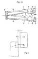
- FIG. 1is a schematic view of this switching device.
- mobile element 2or swinging element, is able to move between two end positions A and B to selectively interrupt the passage of a light beam through an opening 7 (located in end position B) provided in the substrate of the switching device.
- Electrodes 5 , 6are placed in the vicinity of end positions A and B.
- a control circuit 8is provided to generate electrostatic forces of attraction and/or repulsion for switching the swinging element 2 between the two end positions.
- the swinging element 2is attached to the substrate in an elastic manner (for example by means of a flexible beam 3 which is clamped at one of its end to an anchoring point or base 4 ). More particularly, according to this document, beam 3 is designed in such a way that an elastic return force which tends towards a zero position O has, in an essential amplitude range, a higher value than the electrostatic force of attraction generated by the control circuit and the electrodes. Accordingly, the characteristics of the switching devices, such as its response time, are mainly determined by the mechanical properties of the structure.
- FIG. 2is a schematic view of this other switching device. Electrodes 5 , 6 are provided along the whole length of the flexible beam 3 which connects the swinging element 2 to the substrate. Stoppers 9 are further provided on both sides of flexible beam 3 along its length in order to avoid short-circuits between the beam and the electrodes.
- the switching deviceis actuated by means of attractive forces, i.e. the electrodes are disposed laterally with respect to the mobile element's trajectory so as to produce electrostatic forces which are substantially normal to the cooperating edges of the electrodes and of the swinging element. Stoppers are therefore typically required to limit the displacement of the mobile element as well as prevent any short-circuit between the electrodes and the mobile element.
- the contact between the polysilicon surface (or other material) and the stoppersmay lead to extensive wear and debris production and can eventually lead to sticking of the mobile element.
- the so-called “stiction problem”(which also encompasses problems due to capillarity forces or organic and non-organic contamination) Is a well-known and very actual and critical problem with micromechanical switching devices.
- the sticking effectincreases with the inverse of the scale down factor, with a preponderance effect due to humidity, surface trapped charges or other proximity forces (such as quantum Van de Walls forces). These sticking forces are in the same order of magnitude than the activation forces (around 0.2 ⁇ N/ ⁇ m 2 ). They therefore have significant influence on the reliability of such systems.
- Another solutionis to chemically treat the device surfaces and for instance coat the device with an additional layer such as a polymer.
- This solutionhowever increases the fabrication complexity of the device as well as its costs.
- excessive wear of this coating layercan nevertheless give rise to the above stiction problem.
- a principal object of the present inventionis thus to provide a solution that is not prone to stiction problems and that is as much as possible independent of the drive and technological tolerances to control the displacements of the mobile element of the switching device.
- Another object of the present inventionis to provide a solution that is not unnecessarily complicated to manufacture.
- a secondary object of the present inventionis to provide a switching device that can be arranged in a matrix configuration.
- switching unitcomprising a number of such switching device, as well as a method for actuating a switching device the features of which are listed in claim 21 .
- the actuating electrodesare not disposed to act laterally on the mobile element so as to produce attractive electrostatic forces but act on a frontal edge of the mobile element (that is an edge which is substantially parallel to the mobile element's trajectory).
- This driving principlemay be called “Edge Electrostatic Drive”, that is the movement of the mobile element is not caused by attractive forces generated by the actuating electrodes (as in the prior art solutions), but is rather caused by lateral forces which are substantially parallel to the cooperating frontal edges of the stationary electrodes and of the electrode of the mobile element.
- an attractive electrostatic forceshall mean an electrostatic force which tends to bring the cooperating edges of the electrodes nearer (or, conversely, which tends to separate these cooperating edges), whereas a lateral electrostatic force shall mean an electrostatic force which tends to align the cooperating edges of the electrodes one with respect to the other.
- the switching devicecan truly be designed as a contact-less structure which is not affected by the above-mentioned stiction problems. Indeed, stoppers are not anymore required to define the end positions of the mobile element. As a matter of fact, the mobile element is auto-stabilized in its selected position due to the inversion of the forces resulting from the sum of the lateral electrostatic forces and mechanical spring forces exerted on the device's mobile element.
- the geometry of the deviceis selected to enhance the contributions of lateral electrostatic forces.
- the device's switching positionsare determined by an equilibrium point between the lateral electrostatic forces produced by the electrodes on the device's mobile element and mechanical spring forces produced by the elastic member that connects the mobile element to the device's base member. The force resulting from the sum of these lateral electrostatic force and mechanical spring force presents an inversion point around this equilibrium point
- the switching deviceis used as a shutter device for selectively interrupting the passage of a light beam, the switching device being provided with an opening, which is either open or dosed by a screen plate.
- the switching devicecomprises an optical deflecting member disposed perpendicularly to the plane of movement of the switching device.
- Such devicecan be used as a shutter or mirror for light beams produced parallel to the switching device's plane.
- the switching deviceis used as a deflectable device and performs the operation of so-called “deformable mirror devices” or DMDs, the switching device being provided with a controllable screen plate comprising a reflective surface, this controllable screen plate being rotated around at least one axis of rotation.
- the present inventioncan advantageously be applied in optical application to interrupt, modulate or control the passage of light beams but is however not limited to that particular type of applications.
- FIG. 1schematically shows a first switching device of the prior art
- FIG. 2schematically shows a known improvement of the switching device of FIG. 1;
- FIG. 3schematically shows a first embodiment of the switching device according to the present invention
- FIG. 4schematically shows a second embodiment of the switching device according to the present invention.
- FIG. 4 aschematically shows a variant of the second embodiment of FIG. 3 ;
- FIG. 5schematically shows a parallel electrode configuration and the contribution of the attractive and lateral electrostatic forces
- FIG. 6is a perspective view illustrating the out-of-plane deviation of the free-standing structure of FIG. 4 a due to internal stress profile between the different layers of the structure and the proposed beam configuration for compensating for this deviation on the mobile element's side;
- FIG. 7schematically shows a third embodiment of the switching device according to the present invention.
- FIG. 8schematically shows a fourth embodiment of the switching device according to the present invention.
- FIG. 9schematically shows a fifth embodiment of the switching device according to the present invention comprising comb-shaped electrode structures
- FIGS. 10 a and 10 bare respectively a schematic top view and a partial side view of a sixth embodiment of the present invention in the form of a two-axis deformable or steerable mirror device;
- FIG. 11schematically shows a two-dimensional switching unit comprising an array of four switching devices similar to the switching device of FIG. 4 a;
- FIG. 12schematically illustrates the evolution of the lateral electrostatic force and of the mechanical spring force exerted on the switching device's mobile element according to a preferred embodiment of the present invention
- FIG. 13schematically illustrates a partial view of a switching device according to the present invention further carrying an optical deflecting screen plate disposed on the mobile element perpendicularly to the plane of movement of the switching device;
- FIG. 14schematically illustrates an optical switching device comprising an array of 4 ⁇ 4 switching devices as illustrated in FIG. 13 .
- FIG. 3schematically shows a switching device constituting a first embodiment of the present invention.
- a mobile element 2comprising a screen in the form of a plate 20 is attached to one end of an elastic rod or beam 3 .
- the other end of the elastic beam 3is clamped in an anchoring point or base 4 .
- the elastic beam 3extends, in a zero or rest position O, along an axis “x” indicated here for the purpose of explanation.
- Screen plate 20 and beam 3form an oscillating mechanical system wherein screen plate 20 can move back and forth, here between two predetermined switching positions indicated by references A and B, along a direction substantially parallel to an axis “y” perpendicular to axis “x”. It will be appreciated that only one or more than two predetermined switching positions could be defined. According to this embodiment, one will actually note that the screen plate's trajectory follows a curved path and is not strictly speaking parallel to axis y.
- the degree of curvature of the trajectory of screen plate 20is dependent on the actual length of beam 3 and can thus be limited provided that the beam length is sufficiently high as compared to the global course of the mobile element.
- the mobile element's trajectoryis substantially parallel to axis y.
- FIG. 4schematically shows a second embodiment of the present invention.
- the mobile element 2comprising the screen plate 20 Is connected to two anchoring points or bases 4 by means of an elastic member.
- the elastic memberhere consists of a folded beam structure having, In this particular example, essentially an “E” shape.
- This folded beam structurecomprises a first pair of beams 30 (a single beam could however be used) extending from base 4 to an intermediate member 32 in a direction substantially parallel to the plane of the substrate.
- a second beam 3extends from intermediate member 32 to screen plate 20 in a second direction substantially opposite to the first direction.
- the geometry of the folded beam structure which elastically connects screen plate 20 to base 4may take any other adequate form than that illustrated in FIG. 4 .
- intermediate member 32may be reduced in size so as to save some space on the substrate's surface, and first beams 30 may extend in a slightly oblique manner as shown in FIG. 4 a .
- This latter configurationallows a higher density of switching devices to be accommodated on the same substrate.
- the elastic beams 3 , 30extend, in a zero or rest position O, along an axis “x” indicated here for the purpose of explanation.
- Screen plate 20 , beams 3 , 30 and intermediate member 32form an oscillating mechanical system wherein screen plate 20 can move back and forth, here between two predetermined switching positions indicated by references A and B, along a direction substantially parallel to an axis “y”, perpendicular to axis “x”. It will again be appreciated that only one or more than two predetermined switching positions could be defined.
- the screen plate's trajectoryalso follows a curved path and is not strictly speaking parallel to axis y.
- the degree of curvature of the trajectory of screen plate 20is dependent on the actual length of beam 3 and can thus be limited provided that the beam length is sufficiently high as compared to the global course of the mobile element.
- the mobile element's trajectoryis substantially parallel to axis y.
- stationary actuating electrodes 5 and 6 for displacing screen plate 20are respectively disposed in the vicinity of positions A and B.
- Actuating electrodes 5 , 6 and screen plate 20which is also covered by an electrode, are electrically connected to a control circuit 8 which can switch the switching device.
- Each one of electrodes 5 , 6comprises a so-called frontal edge 5 a , 6 a which cooperates with a frontal edge 20 a of screen plate 20 .
- the frontal edge 20 a of screen plate 20may partially overlap the frontal edges of actuating electrodes 5 , 6 .
- the control circuit 8can conveniently be used for adjusting the switching position of the mobile element 2 , for instance by varying the control voltage.
- the electrodesare not disposed to act on the lateral edge of the screen plate 20 (that is an edge which is substantially perpendicular to the screen plate's trajectory) but act on the frontal edge 20 a of screen plate 20 , that is an edge which is substantially parallel to the screen plate's trajectory, or, in other words, an edge which extends along a direction substantially parallel to axis y in FIGS. 3 and 4.
- This driving principlemay be called “Edge Electrostatic Drive”, that is the movement of screen plate 20 is not caused by attractive forces generated by the actuating electrodes (as in the prior art solutions), but is rather caused by lateral forces which are substantially parallel to the cooperating edges of the stationary electrodes and of the electrode of the screen plate.
- Expressions (1) and (2) hereinbeloware respectively simplified expressions of the attractive force F n and of the lateral force F t , in the case of a parallel electrode configuration as illustrated in FIG. 5 :
- F n⁇ ⁇ ⁇ t ⁇ ⁇ R ⁇ ⁇ U ⁇ 2 2 ⁇ g 2 ( 1 )
- F t⁇ ⁇ ⁇ t ⁇ ⁇ U 2 2 ⁇ g ( 2 )
- the switching deviceis auto-stabilized by saturation in the electrostatic drive, that is the structure does not require any stoppers to delimit the end positions of screen plate 20 .
- the geometry of the mobile element, elastic member and stationary actuating electrodesis selected so that the mobile element cannot come into contact with either one of the actuating electrodes and that the predetermined switching positions are each defined by an equilibrium point between the lateral electrostatic forces produced on the mobile element by the stationary actuating electrodes and the mechanical springs forces produced by the elastic member.
- the force resulting from the sum of these lateral electrostatic forces and mechanical spring forceshas opposite directions around this equilibrium point.
- FIG. 12schematically illustrates the evolution of the lateral electrostatic forces (curve a) and mechanical spring forces (curve b, which is a substantially linear curve) in the vicinity of the equilibrium point (indicated by reference E) according to a preferred embodiment of the invention.
- the geometry of the mobile element, elastic member and stationary actuating electrodesis selected in such a way that the lateral electrostatic forces exhibit a steep drop of intensity close to the equilibrium point.
- each switching position of the devicewill be defined by the point of inversion of the lateral electrostatic forces. This point of inversion would coincide with a substantially symmetrical position of the mobile element with respect to the corresponding stationary actuating electrode.
- each switching positionwill be defined by an equilibrium point (point E in FIG. 12) between the lateral electrostatic forces and mechanical spring forces (i.e. the intersection of curves a and b in FIG. 12 ). This equilibrium point E is closer to the zero position of the switching device than the point where inversion of the lateral electrostatic forces occurs.
- the attractive electrostatic forces which are still generated by the actuating electrodesproduce a reaction on screen plate 20 which may be qualified as “lateral surfing”. Indeed, the attractive electrostatic forces tend to attract screen plate 20 towards the actuated electrode. Since screen plate 20 is however retained by beam 3 , plate 20 Is subjected to a torque which further pulls mobile element 2 to its selected position.
- the mobile elementsince the mobile element is essentially moved and held in place due to contributions of lateral electrostatic forces, its switching position can be adjusted by varying the control voltage applied to the electrodes.
- This possibility to adjust the switching position of the switching device through the applied control voltageis highly advantageous, in particular in optical applications where accuracy is a critical element. Indeed, it is now possible to effectively trim and adjust the device's effective switching position to correct positioning errors due to manufacturing tolerances and even recalibrate the device over time to compensate for drifting phenomena. In that regard.
- frontal edge 20 a of screen plate 20that is the outermost edge of screen plate 20 , is preferably designed to have a curved profile so that the gap between screen plate 20 and the electrodes 5 , 6 can be reduced, thereby increasing the sensitivity of the device, and without fearing for short-circuits to happen between the actuating electrodes and the mobile element.
- actuating electrodes 5 , 6are shown to have an oblique edge, but it will dearly be understood that these electrodes may exhibit any other suitable profile such as for instance a curved profile essentially matching the envelope of the screen plate axis extremity, or even a stepped profile.
- the above switching device as well as the switching structures which will be described beloware typically produced in a substrate (made of, for example, silicon or a transparent material such as glass) according to surface micro-machining techniques well-known in the art.
- the free-standing structures(such as screen plate 20 , intermediate member 32 and beams 3 , 30 in FIG. 4) may typically be fabricated using so-called sacrificial layer techniques, that is the movable structure of the switching device is firstly formed on top of a sacrificial layer or spacer and portions of this sacrificial layer are subsequently removed to release the required parts of the switching device.
- Screen plate 20is essentially square (having a surface area of approximately 35 ⁇ 35 ⁇ m 2 and a thickness of about 2 ⁇ m) and is attached to the end of beam 3 (having a length of about 350 to 400 ⁇ m and a section of about 2.5 ⁇ 2 ⁇ m 2 ).
- Screen plate 20 , intermediate member 32 and beams 3 , 30can be made, for example, of metal or polysilicon (or any other crystalline or polycrystalline material). Beams 3 and 30 , being long and thin, are elastically deformable so as to allow a swinging movement of screen plate 20 In a plane substantially parallel to the substrate's plane.
- FIG. 6shows a perspective view of the switching device of FIG. 4 a which illustrates this compensation mechanism.
- the superposition of different layers of material on the free-standing structure of the switching devicein particular the superposition of polysilicon and metal layers, causes a deviation out of the substrate's plane (substrate is indicated by reference numeral 10 ) of the elastic folded beam structure. Since the first beams 30 and the second beam 3 extend in substantially opposite directions, the deviation on the intermediate member's side is essentially compensated on the screen plate's side.
- FIG. 7shows a third embodiment of the present invention.
- switching device 1is provided with means for guiding screen plate 20 in a substantially linear way.
- the single beam structure of FIG. 3is replaced by a parallel or pantograph-like structure.
- This parallel beam structurecan easily be realized by means of a pair of parallel flexible beams indicated by reference numerals 35 and 36 .
- Such a parallel configurationcauses screen plate 20 to be guided linearly and not anymore rotated as this is the case with the above-described solutions.
- the frontal edge 20 a of screen plate 20does not therefore require to be curved and the gap between screen plate 20 and actuating electrodes 5 , 6 can be kept almost constant.
- the parallel structure which has just been describedcan also be combined with the folded beam structure of FIG. 4 as illustrated by the fourth embodiment of FIG. 8 .
- the elastic member connecting screen plate 20 to the base 4there comprises a first pair of parallel flexible beams 33 , 34 extending from base 4 (there are actually two bases in this example) to intermediate member 32 , and a second pair of parallel flexible beams 35 , 36 extending from intermediate member 32 to screen plate 20 in an opposite direction.
- the gap between screen plate and actuating electrodes 5 , 6can be kept constant.
- actuating electrodes 5 , 6cooperate with the frontal edge 20 a of screen plate 20 (the outermost edge of screen plate 20 ). It will however be appreciated that the driving principle according to the present invention can be applied to any other suitable edge of mobile element 2 provided that this edge is substantially parallel to the mobile element's trajectory.
- mobile element 2may advantageously be provided with one or more teeth that extend substantially perpendicularly from the axis of beam 3 and cooperate with an adequate electrode structure.
- the switching devicemay be equipped with comb-shaped electrode structures, that is two interpenetrating comb-shaped structures that cooperate together and which are provided, on the one hand, on mobile element 2 and, on the other hand, on actuating electrodes 5 , 6 .
- FIG. 9shows an example of the switching device according to the present Invention which is equipped with comb-shaped electrode structures, this device being essentially similar to the device of FIG. 8 .
- Comb-shaped structures 25are provided on each side of mobile element 2 and cooperate with comb-shaped structures 55 and 65 provided on actuating electrodes 5 and 6 respectively.
- Each tooth of comb-shaped structures 25 , 55 and 65extends in a direction substantially parallel to the mobile element's trajectory, and comprises an end portion 25 a , 55 a , 65 a of greater dimensions or diameter than that of the portion which connects the tooth to mobile element 2 or actuating electrodes 5 , 6 , respectively. Accordingly, lateral electrostatic forces will also be produced by the actuating electrodes on each tooth of mobile element 2 .
- the pair of parallel flexible beams 33 , 34 which connect base 4 to intermediate member 32are located between the second pair of parallel flexible beams 35 , 36 that connect intermediate member 32 to mobile element 2 .
- Base 4can therefore advantageously act as a security stopper against external shocks.
- An advantage of the switching device of FIG. 9resides in the fact that high air damping of the structure can be achieved between the teeth of the comb-shaped structures. Associated with the electrostatic brake which is increased by the comb-shaped structures, this air damping contributes to reducing the setting time of the device.
- deformable mirror structurescan easily be adapted to use the above driving principle.
- the deflectable elementcould be operated by providing actuating electrodes that cooperate with the lateral edges of the deflectable element.
- deformable mirror devicescould be of the torsion, flexural or cantilever type.
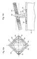
- FIGS. 10 a and 10 billustrate a particularly advantageous and simple example of a steerable mirror device operated according to the present invention.
- FIG. 10 ais a top view of this steerable mirror device comprising a mobile element 102 including a screen plate 120 (which may typically comprise a reflective surface) connected to the substrate by an elastic member indicated globally by reference numeral 103 .
- the elastic member 103is designed to allow mobile element 102 to rotate around two perpendicular axes and comprises outer 130 and inner 135 frames.
- Outer frame 130Is damped in an anchoring point or base (not shown) attached to the substrate and is connected to inner frame 135 by means of two torsion beams 131 , 132 which define the first axis of rotation of mobile element 102 .
- Inner frame 135is connected to mobile element 102 by means of two torsion beams 136 , 137 which define the second axis of rotation of mobile element 102 .
- FIG. 10 bis a partial side view of the device of FIG. 9 a which illustrates how the device is operated.
- Mobile element 102comprises an actuating member 125 which extends substantially perpendicularly from screen plate 120 towards the substrate 110 .
- a pair of actuating electrodes 105 , 106is provided underneath mobile element 102 , on the substrate's surface, in the vicinity of the actuating members tip or extremity 125 a .
- a second pair of similar actuating electrodes(not shown) is disposed along the other axis to allow deflection of the mobile element 102 around the other axis of rotation.
- Actuating member 125is selectively moved from one side to the other In exactly the same way as this is the case with screen plate 20 In the embodiment of FIG. 4, lateral electrostatic forces being applied to the actuating member 125 by means of actuating electrodes 105 , 106 .
- FIG. 11schematically shows four switching devices S 1 to S 4 (similar to the switching device of FIG. 4 a ) which are arranged in two rows and two columns.
- the two actuating electrodes of switching devices S 1 and S 3are connected together by two column lines A 1 and B 1 , respectively.
- the two actuating electrodes of switching devices S 2 and S 4are connected together by two column lines A 2 and B 2 .
- the bases of switching devices S 1 and S 2on the one hand, and of switching devices S 3 and S 4 , on the other hand, are connected together on a row line R 1 and R 2 , respectively.
- each switching devicecan be addressed individually by selectively activating the adequate row and column lines. It will also be appreciated that the specific arrangement of FIG. 11 is purely illustrative and is in no way limitative, and that the switching devices will in practice be organized in such way as to take as little space as possible to increase the density of such devices on the substrate.
- FIG. 13Is a partial top view of a switching device according to the present invention and showing the switching device's mobile element 2 and screen plate 20 , and part of the elastic member 3 connecting this mobile element 2 to its damped base (not shown in this drawing).
- This switching devicemay be any one of the above described switching devices or, preferably, the one illustrated in FIG. 7 .
- FIG. 13further shows a deflecting screen plate 200 disposed on screen plate 20 perpendicularly to the plane of movement of the switching device (i.e. perpendicularly to the plane of the drawing). This deflecting screen plate 200 could be used to interrupt or deflect lights beams produced in a plane parallel to the plane of movement of the switching device.
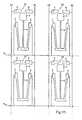
- FIG. 14schematically illustrates an optical switching device 500 comprising an array of 4 ⁇ 4 switching devices (diagonal lines in the figure) as illustrated in FIG. 13 .
- the switching device 500comprises a first optical input 501 and two optical output 502 , 503 , each receiving four optical fibers a 1 to d 1 , a 2 to d 2 and a 3 to d 3 respectively.
- Light beams applied on each one of the input fibers al to d 1may be selectively directed to either one of the two outputs 502 , 503 by means of the switching device array.
- two switching devices 201 , 202are shown to be actuated (shown in thick lines) to respectively deflect the light beams of input fibers a 1 , b 1 to output fibers a 2 , b 2 .
- FIG. 14also shows that the light beams of optical fibers c 1 and d 1 are not deflected and are transmitted to output fibers c 3 and d 3 respectively. It should be pointed out that, as mentioned above, it is particularly important to be able to adjust the position of the switching devices when actuated. Providing as many control circuits as switching devices would allows this to be done.
Landscapes
- Physics & Mathematics (AREA)
- General Physics & Mathematics (AREA)
- Optics & Photonics (AREA)
- Mechanical Light Control Or Optical Switches (AREA)
- Micromachines (AREA)
- Apparatuses For Generation Of Mechanical Vibrations (AREA)
- Adhesives Or Adhesive Processes (AREA)
- Semiconductor Lasers (AREA)
- Gyroscopes (AREA)
Abstract
Description


Claims (21)
Applications Claiming Priority (6)
| Application Number | Priority Date | Filing Date | Title |
|---|---|---|---|
| EP01203752.9 | 2001-10-04 | ||
| EP01203752 | 2001-10-04 | ||
| EP01203752 | 2001-10-04 | ||
| EP01203749 | 2001-10-04 | ||
| EP01203749 | 2001-10-04 | ||
| EP01203749.5 | 2001-10-04 |
Publications (2)
| Publication Number | Publication Date |
|---|---|
| US20030068118A1 US20030068118A1 (en) | 2003-04-10 |
| US6701039B2true US6701039B2 (en) | 2004-03-02 |
Family
ID=26077009
Family Applications (1)
| Application Number | Title | Priority Date | Filing Date |
|---|---|---|---|
| US10/260,541Expired - LifetimeUS6701039B2 (en) | 2001-10-04 | 2002-10-01 | Switching device, in particular for optical applications |
Country Status (10)
| Country | Link |
|---|---|
| US (1) | US6701039B2 (en) |
| EP (1) | EP1300714B1 (en) |
| JP (1) | JP4238132B2 (en) |
| KR (1) | KR100944203B1 (en) |
| AT (1) | ATE333105T1 (en) |
| AU (1) | AU2002362541B2 (en) |
| CA (1) | CA2462812C (en) |
| DE (1) | DE60213051T2 (en) |
| DK (1) | DK1300714T3 (en) |
| WO (1) | WO2003029874A2 (en) |
Cited By (49)
| Publication number | Priority date | Publication date | Assignee | Title |
|---|---|---|---|---|
| US20050264131A1 (en)* | 2004-05-28 | 2005-12-01 | Samsung-Electro Mechanics Co., Ltd. | Rotary-type comb-drive actuator and variable optical attenuator using the same |
| US20060187190A1 (en)* | 2005-02-23 | 2006-08-24 | Pixtronix, Incorporated | Display methods and apparatus |
| US20060187528A1 (en)* | 2005-02-23 | 2006-08-24 | Pixtronix, Incorporated | Methods and apparatus for spatial light modulation |
| US20060187529A1 (en)* | 2005-02-23 | 2006-08-24 | Pixtronix, Incorporated | Display methods and apparatus |
| US20060187531A1 (en)* | 2005-02-23 | 2006-08-24 | Pixtronix, Incorporated | Methods and apparatus for bi-stable actuation of displays |
| US20060187530A1 (en)* | 2005-02-23 | 2006-08-24 | Pixtronix, Incorporated | Methods and apparatus for actuating displays |
| US20060187191A1 (en)* | 2005-02-23 | 2006-08-24 | Pixtronix, Incorporated | Display methods and apparatus |
| US20060214534A1 (en)* | 2005-03-28 | 2006-09-28 | Maurice Thomas | Versatile digitally controlled micro-mechanical actuator |
| US20060256039A1 (en)* | 2005-02-23 | 2006-11-16 | Pixtronix, Incorporated | Display methods and apparatus |
| US20070002156A1 (en)* | 2005-02-23 | 2007-01-04 | Pixtronix, Incorporated | Display apparatus and methods for manufacture thereof |
| US20070279727A1 (en)* | 2006-06-05 | 2007-12-06 | Pixtronix, Inc. | Display apparatus with optical cavities |
| US20080094853A1 (en)* | 2006-10-20 | 2008-04-24 | Pixtronix, Inc. | Light guides and backlight systems incorporating light redirectors at varying densities |
| US20080158635A1 (en)* | 2005-02-23 | 2008-07-03 | Pixtronix, Inc. | Display apparatus and methods for manufacture thereof |
| US20090034052A1 (en)* | 2005-02-23 | 2009-02-05 | Pixtronix, Inc. | Methods and apparatus for actuating displays |
| US20090244678A1 (en)* | 2005-02-23 | 2009-10-01 | Pixtronix, Inc. | Display apparatus and methods for manufacture thereof |
| US7616368B2 (en) | 2005-02-23 | 2009-11-10 | Pixtronix, Inc. | Light concentrating reflective display methods and apparatus |
| US7675665B2 (en) | 2005-02-23 | 2010-03-09 | Pixtronix, Incorporated | Methods and apparatus for actuating displays |
| US20100110518A1 (en)* | 2008-10-27 | 2010-05-06 | Pixtronix, Inc. | Mems anchors |
| US7746529B2 (en) | 2005-02-23 | 2010-06-29 | Pixtronix, Inc. | MEMS display apparatus |
| US20100188443A1 (en)* | 2007-01-19 | 2010-07-29 | Pixtronix, Inc | Sensor-based feedback for display apparatus |
| US7839356B2 (en) | 2005-02-23 | 2010-11-23 | Pixtronix, Incorporated | Display methods and apparatus |
| US7852546B2 (en) | 2007-10-19 | 2010-12-14 | Pixtronix, Inc. | Spacers for maintaining display apparatus alignment |
| US7920317B2 (en) | 2008-08-04 | 2011-04-05 | Pixtronix, Inc. | Display with controlled formation of bubbles |
| US20110148948A1 (en)* | 2005-02-23 | 2011-06-23 | Pixtronix, Inc. | Circuits for controlling display apparatus |
| KR101157502B1 (en)* | 2005-02-23 | 2012-06-15 | 픽스트로닉스 인코포레이티드 | Methods and apparatus for actuating displays |
| US8248560B2 (en) | 2008-04-18 | 2012-08-21 | Pixtronix, Inc. | Light guides and backlight systems incorporating prismatic structures and light redirectors |
| US8310442B2 (en) | 2005-02-23 | 2012-11-13 | Pixtronix, Inc. | Circuits for controlling display apparatus |
| US8482496B2 (en) | 2006-01-06 | 2013-07-09 | Pixtronix, Inc. | Circuits for controlling MEMS display apparatus on a transparent substrate |
| US20130194649A1 (en)* | 2012-01-26 | 2013-08-01 | Tiansheng ZHOU | Rotational Type of MEMS Electrostatic Actuator |
| US8520285B2 (en) | 2008-08-04 | 2013-08-27 | Pixtronix, Inc. | Methods for manufacturing cold seal fluid-filled display apparatus |
| US8519945B2 (en) | 2006-01-06 | 2013-08-27 | Pixtronix, Inc. | Circuits for controlling display apparatus |
| US8526096B2 (en) | 2006-02-23 | 2013-09-03 | Pixtronix, Inc. | Mechanical light modulators with stressed beams |
| US8749538B2 (en) | 2011-10-21 | 2014-06-10 | Qualcomm Mems Technologies, Inc. | Device and method of controlling brightness of a display based on ambient lighting conditions |
| US9082353B2 (en) | 2010-01-05 | 2015-07-14 | Pixtronix, Inc. | Circuits for controlling display apparatus |
| US9135868B2 (en) | 2005-02-23 | 2015-09-15 | Pixtronix, Inc. | Direct-view MEMS display devices and methods for generating images thereon |
| US9134552B2 (en) | 2013-03-13 | 2015-09-15 | Pixtronix, Inc. | Display apparatus with narrow gap electrostatic actuators |
| US9170421B2 (en) | 2013-02-05 | 2015-10-27 | Pixtronix, Inc. | Display apparatus incorporating multi-level shutters |
| US9176318B2 (en) | 2007-05-18 | 2015-11-03 | Pixtronix, Inc. | Methods for manufacturing fluid-filled MEMS displays |
| US9183812B2 (en) | 2013-01-29 | 2015-11-10 | Pixtronix, Inc. | Ambient light aware display apparatus |
| WO2015191664A1 (en)* | 2014-06-10 | 2015-12-17 | Agiltron, Inc. | Micro-machined optical mirror switch |
| US9229222B2 (en) | 2005-02-23 | 2016-01-05 | Pixtronix, Inc. | Alignment methods in fluid-filled MEMS displays |
| US9261694B2 (en) | 2005-02-23 | 2016-02-16 | Pixtronix, Inc. | Display apparatus and methods for manufacture thereof |
| US9291813B2 (en) | 2010-12-20 | 2016-03-22 | Pixtronix, Inc. | Systems and methods for MEMS light modulator arrays with reduced acoustic emission |
| US9398666B2 (en) | 2010-03-11 | 2016-07-19 | Pixtronix, Inc. | Reflective and transflective operation modes for a display device |
| US9606349B2 (en) | 2015-01-05 | 2017-03-28 | Edward Pakhchyan | MEMS display |
| US9703095B2 (en) | 2015-01-05 | 2017-07-11 | Edward Pakhchyan | Light modulator for MEMS display |
| US9703094B2 (en) | 2015-01-05 | 2017-07-11 | Edward Pakhchyan | MEMS light modulator for display |
| US11009650B2 (en) | 2015-01-05 | 2021-05-18 | Edward Pakhchyan | MEMS display |
| US12054384B2 (en) | 2018-05-17 | 2024-08-06 | Fraunhofer-Gesellschaft Zur Foerderung Der Angewandten Forschung E. V. | MEMS comprising a movable structural element, and MEMS array |
Families Citing this family (14)
| Publication number | Priority date | Publication date | Assignee | Title |
|---|---|---|---|---|
| US7250611B2 (en)* | 2003-12-02 | 2007-07-31 | 3M Innovative Properties Company | LED curing apparatus and method |
| JP2005227591A (en)* | 2004-02-13 | 2005-08-25 | Murata Mfg Co Ltd | Electrostatic type actuator |
| US7119942B2 (en)* | 2004-06-30 | 2006-10-10 | Northrop Gruman Corporation | Side spring micro-mirror |
| CN102060258B (en)* | 2005-02-23 | 2013-07-10 | 皮克斯特隆尼斯有限公司 | Microelectronic mechanical shutter device |
| US7656568B2 (en)* | 2005-05-18 | 2010-02-02 | The Regents Of The University Of California | Optical switch using frequency-based addressing in a microelectromechanical systems array |
| JP2007074826A (en)* | 2005-09-07 | 2007-03-22 | Fujifilm Corp | Microelectromechanical element and microelectromechanical element array |
| US7832948B1 (en)* | 2007-09-13 | 2010-11-16 | Tessera MEMS Technologies, Inc. | Impulse actuated MEMS devices |
| TWI418850B (en)* | 2007-11-09 | 2013-12-11 | 尼康股份有限公司 | Micro-actuator, optical device, display device, exposure device and device production method |
| WO2009102471A1 (en)* | 2008-02-12 | 2009-08-20 | Pixtronix, Inc. | Mechanical light modulators with stressed beams |
| JP5714517B2 (en)* | 2012-01-30 | 2015-05-07 | シャープ株式会社 | Backlight, liquid crystal display device including the backlight, and backlight lighting method |
| US10132699B1 (en)* | 2014-10-06 | 2018-11-20 | National Technology & Engineering Solutions Of Sandia, Llc | Electrodeposition processes for magnetostrictive resonators |
| JP6953118B2 (en)* | 2016-07-04 | 2021-10-27 | エドワード・パクチャン | MEMS light modulators for displays |
| US11079066B2 (en) | 2016-10-29 | 2021-08-03 | Philippe Roe | Fiber optic safety system |
| CN110725773B (en)* | 2019-11-06 | 2020-09-04 | 北京纳米能源与系统研究所 | Underwater energy collecting device and underwater operation equipment |
Citations (8)
| Publication number | Priority date | Publication date | Assignee | Title |
|---|---|---|---|---|
| US5367585A (en)* | 1993-10-27 | 1994-11-22 | General Electric Company | Integrated microelectromechanical polymeric photonic switch |
| US6396976B1 (en)* | 1999-04-15 | 2002-05-28 | Solus Micro Technologies, Inc. | 2D optical switch |
| US6396975B1 (en)* | 2000-01-21 | 2002-05-28 | Jds Uniphase Corporation | MEMS optical cross-connect switch |
| US20020181855A1 (en)* | 2001-04-13 | 2002-12-05 | Xin Xue | Electrically controllable integrated optical cross-connect |
| US20030012488A1 (en)* | 2001-07-03 | 2003-01-16 | Bevan Staple | MEMS-based noncontacting free-space optical switch |
| US6577785B1 (en)* | 2001-08-09 | 2003-06-10 | Sandia Corporation | Compound semiconductor optical waveguide switch |
| US6587612B1 (en)* | 2000-09-06 | 2003-07-01 | Southwest Research Institute | Thermally actuated spectroscopic optical switch |
| US6597048B1 (en)* | 2000-12-26 | 2003-07-22 | Cornell Research Foundation | Electrostatically charged microstructures |
Family Cites Families (3)
| Publication number | Priority date | Publication date | Assignee | Title |
|---|---|---|---|---|
| DE4224600A1 (en)* | 1992-07-23 | 1994-01-27 | Somatel Sondermaschinenbau Tel | Micro-mechanical electrostatic positioning appts., e.g. for mirror, in Michelson interferometer - has several fixed electrodes producing electrostatic field, applying force to vary position of plate-shaped element |
| FR2726135B1 (en)* | 1994-10-25 | 1997-01-17 | Suisse Electronique Microtech | SWITCHING DEVICE |
| US6595055B1 (en)* | 1998-10-28 | 2003-07-22 | Fraunhofer-Gesellschaft Zur Foerderung Der Angewandten | Micromechanical component comprising an oscillating body |
- 2002
- 2002-10-01USUS10/260,541patent/US6701039B2/ennot_activeExpired - Lifetime
- 2002-10-03ATAT02079138Tpatent/ATE333105T1/ennot_activeIP Right Cessation
- 2002-10-03DKDK02079138Tpatent/DK1300714T3/enactive
- 2002-10-03EPEP02079138Apatent/EP1300714B1/ennot_activeExpired - Lifetime
- 2002-10-03DEDE60213051Tpatent/DE60213051T2/ennot_activeExpired - Lifetime
- 2002-10-04CACA2462812Apatent/CA2462812C/ennot_activeExpired - Fee Related
- 2002-10-04KRKR1020047005064Apatent/KR100944203B1/ennot_activeExpired - Fee Related
- 2002-10-04WOPCT/DK2002/000666patent/WO2003029874A2/enactiveIP Right Grant
- 2002-10-04AUAU2002362541Apatent/AU2002362541B2/ennot_activeCeased
- 2002-10-04JPJP2003533030Apatent/JP4238132B2/ennot_activeExpired - Lifetime
Patent Citations (8)
| Publication number | Priority date | Publication date | Assignee | Title |
|---|---|---|---|---|
| US5367585A (en)* | 1993-10-27 | 1994-11-22 | General Electric Company | Integrated microelectromechanical polymeric photonic switch |
| US6396976B1 (en)* | 1999-04-15 | 2002-05-28 | Solus Micro Technologies, Inc. | 2D optical switch |
| US6396975B1 (en)* | 2000-01-21 | 2002-05-28 | Jds Uniphase Corporation | MEMS optical cross-connect switch |
| US6587612B1 (en)* | 2000-09-06 | 2003-07-01 | Southwest Research Institute | Thermally actuated spectroscopic optical switch |
| US6597048B1 (en)* | 2000-12-26 | 2003-07-22 | Cornell Research Foundation | Electrostatically charged microstructures |
| US20020181855A1 (en)* | 2001-04-13 | 2002-12-05 | Xin Xue | Electrically controllable integrated optical cross-connect |
| US20030012488A1 (en)* | 2001-07-03 | 2003-01-16 | Bevan Staple | MEMS-based noncontacting free-space optical switch |
| US6577785B1 (en)* | 2001-08-09 | 2003-06-10 | Sandia Corporation | Compound semiconductor optical waveguide switch |
Cited By (97)
| Publication number | Priority date | Publication date | Assignee | Title |
|---|---|---|---|---|
| US7129617B2 (en)* | 2004-05-28 | 2006-10-31 | Samsung Electro-Mechanics Co., Ltd. | Rotary-type comb-drive actuator and variable optical attenuator using the same |
| US20050264131A1 (en)* | 2004-05-28 | 2005-12-01 | Samsung-Electro Mechanics Co., Ltd. | Rotary-type comb-drive actuator and variable optical attenuator using the same |
| US20110148948A1 (en)* | 2005-02-23 | 2011-06-23 | Pixtronix, Inc. | Circuits for controlling display apparatus |
| US7999994B2 (en) | 2005-02-23 | 2011-08-16 | Pixtronix, Inc. | Display apparatus and methods for manufacture thereof |
| US20060187531A1 (en)* | 2005-02-23 | 2006-08-24 | Pixtronix, Incorporated | Methods and apparatus for bi-stable actuation of displays |
| US20060187530A1 (en)* | 2005-02-23 | 2006-08-24 | Pixtronix, Incorporated | Methods and apparatus for actuating displays |
| US20060187191A1 (en)* | 2005-02-23 | 2006-08-24 | Pixtronix, Incorporated | Display methods and apparatus |
| US9530344B2 (en) | 2005-02-23 | 2016-12-27 | Snaptrack, Inc. | Circuits for controlling display apparatus |
| US20060187528A1 (en)* | 2005-02-23 | 2006-08-24 | Pixtronix, Incorporated | Methods and apparatus for spatial light modulation |
| US20060256039A1 (en)* | 2005-02-23 | 2006-11-16 | Pixtronix, Incorporated | Display methods and apparatus |
| US20070002156A1 (en)* | 2005-02-23 | 2007-01-04 | Pixtronix, Incorporated | Display apparatus and methods for manufacture thereof |
| US20070091038A1 (en)* | 2005-02-23 | 2007-04-26 | Pixtronix, Incorporated | Methods and apparatus for spatial light modulation |
| US20070159679A1 (en)* | 2005-02-23 | 2007-07-12 | Pixtronix, Incorporated | Methods and apparatus for spatial light modulation |
| US7271945B2 (en) | 2005-02-23 | 2007-09-18 | Pixtronix, Inc. | Methods and apparatus for actuating displays |
| US7304785B2 (en) | 2005-02-23 | 2007-12-04 | Pixtronix, Inc. | Display methods and apparatus |
| US7304786B2 (en) | 2005-02-23 | 2007-12-04 | Pixtronix, Inc. | Methods and apparatus for bi-stable actuation of displays |
| US9500853B2 (en) | 2005-02-23 | 2016-11-22 | Snaptrack, Inc. | MEMS-based display apparatus |
| US20080062500A1 (en)* | 2005-02-23 | 2008-03-13 | Pixtronix, Inc. | Methods and apparatus for spatial light modulation |
| US9336732B2 (en) | 2005-02-23 | 2016-05-10 | Pixtronix, Inc. | Circuits for controlling display apparatus |
| US7365897B2 (en) | 2005-02-23 | 2008-04-29 | Pixtronix, Inc. | Methods and apparatus for spatial light modulation |
| US20080123175A1 (en)* | 2005-02-23 | 2008-05-29 | Pixtronix, Inc. | Methods for manufacturing displays |
| US20080151357A1 (en)* | 2005-02-23 | 2008-06-26 | Pixtronix, Inc. | Methods and apparatus for spatial light modulation |
| US20060187190A1 (en)* | 2005-02-23 | 2006-08-24 | Pixtronix, Incorporated | Display methods and apparatus |
| US20080158635A1 (en)* | 2005-02-23 | 2008-07-03 | Pixtronix, Inc. | Display apparatus and methods for manufacture thereof |
| US7405852B2 (en) | 2005-02-23 | 2008-07-29 | Pixtronix, Inc. | Display apparatus and methods for manufacture thereof |
| US7417782B2 (en) | 2005-02-23 | 2008-08-26 | Pixtronix, Incorporated | Methods and apparatus for spatial light modulation |
| US7460290B2 (en) | 2005-02-23 | 2008-12-02 | Pixtronix, Inc. | Methods and apparatus for spatial light modulation |
| US9274333B2 (en) | 2005-02-23 | 2016-03-01 | Pixtronix, Inc. | Alignment methods in fluid-filled MEMS displays |
| US20090034052A1 (en)* | 2005-02-23 | 2009-02-05 | Pixtronix, Inc. | Methods and apparatus for actuating displays |
| US7502159B2 (en) | 2005-02-23 | 2009-03-10 | Pixtronix, Inc. | Methods and apparatus for actuating displays |
| US7551344B2 (en) | 2005-02-23 | 2009-06-23 | Pixtronix, Inc. | Methods for manufacturing displays |
| US20090244678A1 (en)* | 2005-02-23 | 2009-10-01 | Pixtronix, Inc. | Display apparatus and methods for manufacture thereof |
| US7616368B2 (en) | 2005-02-23 | 2009-11-10 | Pixtronix, Inc. | Light concentrating reflective display methods and apparatus |
| US7619806B2 (en) | 2005-02-23 | 2009-11-17 | Pixtronix, Inc. | Methods and apparatus for spatial light modulation |
| US7636189B2 (en) | 2005-02-23 | 2009-12-22 | Pixtronix, Inc. | Display methods and apparatus |
| US7675665B2 (en) | 2005-02-23 | 2010-03-09 | Pixtronix, Incorporated | Methods and apparatus for actuating displays |
| US9261694B2 (en) | 2005-02-23 | 2016-02-16 | Pixtronix, Inc. | Display apparatus and methods for manufacture thereof |
| US7729037B2 (en) | 2005-02-23 | 2010-06-01 | Pixtronix, Inc. | Methods and apparatus for spatial light modulation |
| US7742016B2 (en) | 2005-02-23 | 2010-06-22 | Pixtronix, Incorporated | Display methods and apparatus |
| US7742215B2 (en) | 2005-02-23 | 2010-06-22 | Pixtronix, Inc. | Methods and apparatus for spatial light modulation |
| US7746529B2 (en) | 2005-02-23 | 2010-06-29 | Pixtronix, Inc. | MEMS display apparatus |
| US7755582B2 (en) | 2005-02-23 | 2010-07-13 | Pixtronix, Incorporated | Display methods and apparatus |
| US9229222B2 (en) | 2005-02-23 | 2016-01-05 | Pixtronix, Inc. | Alignment methods in fluid-filled MEMS displays |
| US7839356B2 (en) | 2005-02-23 | 2010-11-23 | Pixtronix, Incorporated | Display methods and apparatus |
| US9177523B2 (en) | 2005-02-23 | 2015-11-03 | Pixtronix, Inc. | Circuits for controlling display apparatus |
| US9158106B2 (en) | 2005-02-23 | 2015-10-13 | Pixtronix, Inc. | Display methods and apparatus |
| US7898714B2 (en) | 2005-02-23 | 2011-03-01 | Pixtronix, Inc. | Methods and apparatus for actuating displays |
| US9135868B2 (en) | 2005-02-23 | 2015-09-15 | Pixtronix, Inc. | Direct-view MEMS display devices and methods for generating images thereon |
| US20060187529A1 (en)* | 2005-02-23 | 2006-08-24 | Pixtronix, Incorporated | Display methods and apparatus |
| US7927654B2 (en) | 2005-02-23 | 2011-04-19 | Pixtronix, Inc. | Methods and apparatus for spatial light modulation |
| US20080158636A1 (en)* | 2005-02-23 | 2008-07-03 | Pixtronix, Inc. | Methods and apparatus for spatial light modulation |
| US8159428B2 (en) | 2005-02-23 | 2012-04-17 | Pixtronix, Inc. | Display methods and apparatus |
| US9087486B2 (en) | 2005-02-23 | 2015-07-21 | Pixtronix, Inc. | Circuits for controlling display apparatus |
| KR101157502B1 (en)* | 2005-02-23 | 2012-06-15 | 픽스트로닉스 인코포레이티드 | Methods and apparatus for actuating displays |
| US8519923B2 (en) | 2005-02-23 | 2013-08-27 | Pixtronix, Inc. | Display methods and apparatus |
| US8310442B2 (en) | 2005-02-23 | 2012-11-13 | Pixtronix, Inc. | Circuits for controlling display apparatus |
| US7468572B2 (en) | 2005-03-28 | 2008-12-23 | Maurice Thomas | Versatile digitally controlled micro-mechanical actuator |
| US20060214534A1 (en)* | 2005-03-28 | 2006-09-28 | Maurice Thomas | Versatile digitally controlled micro-mechanical actuator |
| US8482496B2 (en) | 2006-01-06 | 2013-07-09 | Pixtronix, Inc. | Circuits for controlling MEMS display apparatus on a transparent substrate |
| US8519945B2 (en) | 2006-01-06 | 2013-08-27 | Pixtronix, Inc. | Circuits for controlling display apparatus |
| US8526096B2 (en) | 2006-02-23 | 2013-09-03 | Pixtronix, Inc. | Mechanical light modulators with stressed beams |
| US9128277B2 (en) | 2006-02-23 | 2015-09-08 | Pixtronix, Inc. | Mechanical light modulators with stressed beams |
| US20070279727A1 (en)* | 2006-06-05 | 2007-12-06 | Pixtronix, Inc. | Display apparatus with optical cavities |
| US7876489B2 (en) | 2006-06-05 | 2011-01-25 | Pixtronix, Inc. | Display apparatus with optical cavities |
| US20080094853A1 (en)* | 2006-10-20 | 2008-04-24 | Pixtronix, Inc. | Light guides and backlight systems incorporating light redirectors at varying densities |
| US8545084B2 (en) | 2006-10-20 | 2013-10-01 | Pixtronix, Inc. | Light guides and backlight systems incorporating light redirectors at varying densities |
| US8262274B2 (en) | 2006-10-20 | 2012-09-11 | Pitronix, Inc. | Light guides and backlight systems incorporating light redirectors at varying densities |
| US20100188443A1 (en)* | 2007-01-19 | 2010-07-29 | Pixtronix, Inc | Sensor-based feedback for display apparatus |
| US9176318B2 (en) | 2007-05-18 | 2015-11-03 | Pixtronix, Inc. | Methods for manufacturing fluid-filled MEMS displays |
| US7852546B2 (en) | 2007-10-19 | 2010-12-14 | Pixtronix, Inc. | Spacers for maintaining display apparatus alignment |
| US8441602B2 (en) | 2008-04-18 | 2013-05-14 | Pixtronix, Inc. | Light guides and backlight systems incorporating prismatic structures and light redirectors |
| US9243774B2 (en) | 2008-04-18 | 2016-01-26 | Pixtronix, Inc. | Light guides and backlight systems incorporating prismatic structures and light redirectors |
| US8248560B2 (en) | 2008-04-18 | 2012-08-21 | Pixtronix, Inc. | Light guides and backlight systems incorporating prismatic structures and light redirectors |
| US7920317B2 (en) | 2008-08-04 | 2011-04-05 | Pixtronix, Inc. | Display with controlled formation of bubbles |
| US8520285B2 (en) | 2008-08-04 | 2013-08-27 | Pixtronix, Inc. | Methods for manufacturing cold seal fluid-filled display apparatus |
| US8891152B2 (en) | 2008-08-04 | 2014-11-18 | Pixtronix, Inc. | Methods for manufacturing cold seal fluid-filled display apparatus |
| US9182587B2 (en) | 2008-10-27 | 2015-11-10 | Pixtronix, Inc. | Manufacturing structure and process for compliant mechanisms |
| US9116344B2 (en) | 2008-10-27 | 2015-08-25 | Pixtronix, Inc. | MEMS anchors |
| US20100110518A1 (en)* | 2008-10-27 | 2010-05-06 | Pixtronix, Inc. | Mems anchors |
| US8599463B2 (en) | 2008-10-27 | 2013-12-03 | Pixtronix, Inc. | MEMS anchors |
| US8169679B2 (en) | 2008-10-27 | 2012-05-01 | Pixtronix, Inc. | MEMS anchors |
| US9400382B2 (en) | 2010-01-05 | 2016-07-26 | Pixtronix, Inc. | Circuits for controlling display apparatus |
| US9082353B2 (en) | 2010-01-05 | 2015-07-14 | Pixtronix, Inc. | Circuits for controlling display apparatus |
| US9398666B2 (en) | 2010-03-11 | 2016-07-19 | Pixtronix, Inc. | Reflective and transflective operation modes for a display device |
| US9291813B2 (en) | 2010-12-20 | 2016-03-22 | Pixtronix, Inc. | Systems and methods for MEMS light modulator arrays with reduced acoustic emission |
| US8749538B2 (en) | 2011-10-21 | 2014-06-10 | Qualcomm Mems Technologies, Inc. | Device and method of controlling brightness of a display based on ambient lighting conditions |
| US20130194649A1 (en)* | 2012-01-26 | 2013-08-01 | Tiansheng ZHOU | Rotational Type of MEMS Electrostatic Actuator |
| US9385634B2 (en)* | 2012-01-26 | 2016-07-05 | Tiansheng ZHOU | Rotational type of MEMS electrostatic actuator |
| US9183812B2 (en) | 2013-01-29 | 2015-11-10 | Pixtronix, Inc. | Ambient light aware display apparatus |
| US9170421B2 (en) | 2013-02-05 | 2015-10-27 | Pixtronix, Inc. | Display apparatus incorporating multi-level shutters |
| US9134552B2 (en) | 2013-03-13 | 2015-09-15 | Pixtronix, Inc. | Display apparatus with narrow gap electrostatic actuators |
| WO2015191664A1 (en)* | 2014-06-10 | 2015-12-17 | Agiltron, Inc. | Micro-machined optical mirror switch |
| US9606349B2 (en) | 2015-01-05 | 2017-03-28 | Edward Pakhchyan | MEMS display |
| US9703095B2 (en) | 2015-01-05 | 2017-07-11 | Edward Pakhchyan | Light modulator for MEMS display |
| US9703094B2 (en) | 2015-01-05 | 2017-07-11 | Edward Pakhchyan | MEMS light modulator for display |
| US11009650B2 (en) | 2015-01-05 | 2021-05-18 | Edward Pakhchyan | MEMS display |
| US12054384B2 (en) | 2018-05-17 | 2024-08-06 | Fraunhofer-Gesellschaft Zur Foerderung Der Angewandten Forschung E. V. | MEMS comprising a movable structural element, and MEMS array |
Also Published As
| Publication number | Publication date |
|---|---|
| WO2003029874A2 (en) | 2003-04-10 |
| DE60213051D1 (en) | 2006-08-24 |
| US20030068118A1 (en) | 2003-04-10 |
| AU2002362541B2 (en) | 2007-07-05 |
| DE60213051T2 (en) | 2007-07-05 |
| DK1300714T3 (en) | 2006-11-13 |
| JP2005504355A (en) | 2005-02-10 |
| JP4238132B2 (en) | 2009-03-11 |
| KR100944203B1 (en) | 2010-02-26 |
| ATE333105T1 (en) | 2006-08-15 |
| CA2462812A1 (en) | 2003-04-10 |
| CA2462812C (en) | 2010-12-14 |
| EP1300714A1 (en) | 2003-04-09 |
| KR20040051598A (en) | 2004-06-18 |
| EP1300714B1 (en) | 2006-07-12 |
| WO2003029874A3 (en) | 2004-03-25 |
Similar Documents
| Publication | Publication Date | Title |
|---|---|---|
| US6701039B2 (en) | Switching device, in particular for optical applications | |
| AU2002362541A1 (en) | Switching device, in particular for optical applications | |
| US6593677B2 (en) | Biased rotatable combdrive devices and methods | |
| US5739941A (en) | Non-linear hinge for micro-mechanical device | |
| US6629461B2 (en) | Biased rotatable combdrive actuator methods | |
| US5794761A (en) | Switching device | |
| US6337760B1 (en) | Encapsulated multi-directional light beam steering device | |
| US20010051014A1 (en) | Optical switch employing biased rotatable combdrive devices and methods | |
| US6813060B1 (en) | Electrical latching of microelectromechanical devices | |
| US7538932B2 (en) | High contrast spatial light modulator | |
| US6713367B2 (en) | Self-aligned vertical combdrive actuator and method of fabrication | |
| US20160315560A1 (en) | In-plane and out-of-plane motion actuator | |
| US7443568B2 (en) | Method and system for resonant operation of a reflective spatial light modulator | |
| US20070258130A1 (en) | Reflective spatial light modulator with high stiffness torsion spring hinge | |
| JP2005043674A (en) | Comb electrostatic actuator and light control device using comb electrostatic actuator | |
| CN101151206A (en) | Method and apparatus for actuating a display | |
| JP2002254399A (en) | Electrostatically actuated micro-electromechanical system(mems) device | |
| US7626745B2 (en) | Diffractive thin-film piezoelectric micromirror and method of producing the same | |
| US6822370B2 (en) | Parallel plate electrostatic actuation of MEMS mirrors | |
| US6977765B1 (en) | Diffractive light modulator using cantilevers | |
| US20030178912A1 (en) | Electrostatically operated device | |
| CN100368861C (en) | Switching device, in particular for optical applications | |
| US7463403B1 (en) | High impedance drive circuit for a micro-electromechanical system device | |
| JP4336123B2 (en) | MEMS element and optical device | |
| LARGE-STROKE | 1 University of Neuchâtel, Institute of Microtechnology, IMT |
Legal Events
| Date | Code | Title | Description |
|---|---|---|---|
| AS | Assignment | Owner name:COLIBRYS S.A., SWITZERLAND Free format text:ASSIGNMENT OF ASSIGNORS INTEREST;ASSIGNORS:BOURGEOIS, CLAUDE;UNDERBJERG, CARSTEN;REEL/FRAME:013569/0890 Effective date:20021108 | |
| FEPP | Fee payment procedure | Free format text:PAYOR NUMBER ASSIGNED (ORIGINAL EVENT CODE: ASPN); ENTITY STATUS OF PATENT OWNER: SMALL ENTITY | |
| FEPP | Fee payment procedure | Free format text:PAYOR NUMBER ASSIGNED (ORIGINAL EVENT CODE: ASPN); ENTITY STATUS OF PATENT OWNER: SMALL ENTITY Free format text:PAYER NUMBER DE-ASSIGNED (ORIGINAL EVENT CODE: RMPN); ENTITY STATUS OF PATENT OWNER: SMALL ENTITY | |
| STCF | Information on status: patent grant | Free format text:PATENTED CASE | |
| FEPP | Fee payment procedure | Free format text:PAT HOLDER CLAIMS SMALL ENTITY STATUS, ENTITY STATUS SET TO SMALL (ORIGINAL EVENT CODE: LTOS); ENTITY STATUS OF PATENT OWNER: SMALL ENTITY Free format text:PAYOR NUMBER ASSIGNED (ORIGINAL EVENT CODE: ASPN); ENTITY STATUS OF PATENT OWNER: SMALL ENTITY Free format text:PAYER NUMBER DE-ASSIGNED (ORIGINAL EVENT CODE: RMPN); ENTITY STATUS OF PATENT OWNER: SMALL ENTITY | |
| FPAY | Fee payment | Year of fee payment:4 | |
| FPAY | Fee payment | Year of fee payment:8 | |
| FPAY | Fee payment | Year of fee payment:12 |