US6700814B1 - Sense amplifier bias circuit for a memory having at least two distinct resistance states - Google Patents
Sense amplifier bias circuit for a memory having at least two distinct resistance statesDownload PDFInfo
- Publication number
- US6700814B1 US6700814B1US10/283,622US28362202AUS6700814B1US 6700814 B1US6700814 B1US 6700814B1US 28362202 AUS28362202 AUS 28362202AUS 6700814 B1US6700814 B1US 6700814B1
- Authority
- US
- United States
- Prior art keywords
- current
- transistor
- sense amplifier
- bit cells
- memory
- Prior art date
- Legal status (The legal status is an assumption and is not a legal conclusion. Google has not performed a legal analysis and makes no representation as to the accuracy of the status listed.)
- Expired - Lifetime, expires
Links
Images


Classifications
- G—PHYSICS
- G11—INFORMATION STORAGE
- G11C—STATIC STORES
- G11C7/00—Arrangements for writing information into, or reading information out from, a digital store
- G11C7/06—Sense amplifiers; Associated circuits, e.g. timing or triggering circuits
- G—PHYSICS
- G11—INFORMATION STORAGE
- G11C—STATIC STORES
- G11C2207/00—Indexing scheme relating to arrangements for writing information into, or reading information out from, a digital store
- G11C2207/06—Sense amplifier related aspects
- G11C2207/063—Current sense amplifiers
Definitions
- This inventionrelates to Magnetoresistive Random Access Memories (MRAMs) and other memories where the memory bit has at least two distinct resistance states, and more particularly to the sensing circuitry for such memories.
- MRAMsMagnetoresistive Random Access Memories
- Non-volatile memory devicessuch as FLASH memories
- FLASHis a major non-volatile memory device in use today. Disadvantages of FLASH memory include high voltage requirements and slow program and erase times. Also, FLASH memory has a poor write endurance of 10 4 -10 6 cycles before memory failure. In addition, to maintain reasonable data retention, the scaling of the gate oxide is restricted by the tunneling barrier seen by the electrons. Hence, FLASH memory is limited in the dimensions to which it can be scaled.
- MRAMmagnetoresistive RAM
- the resistance of the tunnel junctionchanges value depending on the state of polarization of the magnetic layers above and below the tunnel junction.
- the resistancechanges from a lower resistance value when the magnetic fields are aligned in the same direction to a higher resistance value when they are aligned in opposite directions.
- the value changemay be on the order of thirty percent. Therefore, for a low resistance value of 10K ohms, the high resistance value could be about 13K ohms.
- a sense amplifier for an MRAMneeds to detect this difference in value. Because of processing variation in the thickness of the oxide in the tunnel junction, there is a large distribution of resistance values between wafer lots of MRAM circuits.
- the nominal value of the resistance within a waferalso varies, it is useful to detect the state of a bit by comparing the resistance of the tunnel junction in a bit to a nearby midpoint reference that may be formed as a midpoint of a reference bit in the high state and a reference bit in the low state. It is also important to maintain symmetry to balance the loading from the parasitic resistance and capacitance of the bit lines and the column multiplexing.
- MRAM sense amplifiersuse a fixed voltage on a common gate stage to place a fixed voltage across the MRAM cell. Control or voltage reference circuits for such sense amplifiers generate a fixed voltage for the gate of the common gate stage. With large processing variations in the MRAM cell resistance and a fixed voltage across the cell, the MRAM cell provides large variations in current to the sense amplifier, making optimization of the sense amplifier difficult.
- the voltage on the bit line and consequently across the memory cellis a constant value independent of the resistance of the bit. The current change resulting from bit resistance changing from processing lot-to-lot causes inaccuracies with device matching in the sense amplifier, thereby degrading sensing time and accuracy.
- FIG. 1is a schematic diagram of a bias circuit for voltage control of a sense amplifier
- FIG. 2is a schematic diagram of a bias circuit for voltage control of another sense amplifier
- FIG. 3is a schematic diagram of another embodiment of the bias circuit of FIG. 1;
- FIG. 4is a schematic diagram of another embodiment of the bias circuit of FIG. 2 .
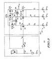
- a memory 113generally having a bias circuit 112 , a sense amplifier 114 and an array portion 116 .
- the bias circuit 112has a P-channel transistor 122 having a first current electrode or a source connected to a power supply voltage terminal V DD .
- a control electrode or gate of transistor 122is connected to a second current electrode or a drain thereof at a node 124 .
- An N-channel transistor 126has a drain connected to the drain of transistor 122 , a gate connected to the output of an operational amplifier 120 , and a source connected to a node 128 .
- Operational amplifier 120has a first or positive (non-inverting) input connected to node 124 at the drain and gate of transistor 122 .
- a second or negative (inverting) input of operational amplifier 120is connected to a node 107 .
- a first terminal of a resistance 130 , R H1is coupled to node 128 .
- a second terminal of resistance 130is coupled to a V SS reference voltage terminal.
- a P-channel transistor 132has a source connected to the V DD terminal, and a gate and a drain connected together and to node 124 and to a drain of an N-channel transistor 134 .
- Transistor 134has a gate connected to the output of operational amplifier 120 and has a source connected to node 128 and coupled to a first terminal of a resistance 136 , R L1 .
- a second terminal of resistance 136is coupled to the V SS terminal.
- the connections to resistance 130 and resistance 136may include coupling devices (not shown) to match the connections of array resistances 177 - 179 of array portion 116 to be described below.
- An operational amplifier 140has a positive input connected to node 124 , and a negative input connected to an output thereof for providing a sense precharge voltage, V B1 .
- An operational amplifier 142has a positive input connected to node 128 , and a negative input connected to an output thereof for providing a bit precharge voltage, V B3 .
- the output of operational amplifier 120provides a common gate bias voltage, V B2 .
- a P-channel transistor 106has a source connected to the V DD terminal, and a gate and drain connected together in a diode-connected configuration and to a node 107 at a negative or inverting input of operational amplifier 120 .
- a current source 108has a first terminal connected to node 107 and a second terminal connected to the V SS terminal.
- a P-channel transistor 144has a source connected to the V DD voltage terminal.
- a drain of transistor 144is connected to a drain of an N-channel transistor 152 at an output node 148 which forms an output terminal labeled OUT.
- a gate of transistor 152is connected to the V B2 common gate bias voltage.
- a source of transistor 152is connected to a node 154 and coupled via one or more coupling devices (not shown) to a first terminal of a bit resistance 177 having a resistance of R B .
- a second terminal of bit resistance 177is coupled via one or more coupling devices (not shown) to the V SS voltage terminal.
- a P-channel transistor 160has a source connected to the V DD voltage terminal, and a gate connected to a drain thereof and to a gate of transistor 144 .
- a switch 150has a first terminal connected to the drain of transistor 144 at node 148 and a second terminal connected to the drain of transistor 160 at node 146 .
- Switch 150is controlled by an Equalization control signal, EQ.
- a drain of an N-channel transistor 162is connected to node 146 .
- Transistor 162has a gate connected to the V B2 common gate bias voltage and has a source connected to a node 164 .
- a first terminal of a high reference resistance 178 , R H2is coupled via one or more coupling devices (not shown) to a node 164 .
- a second terminal of resistance 178is coupled via one or more coupling devices (not shown) to the V SS voltage terminal.
- a P-channel transistor 166has a source connected to the V DD voltage terminal.
- a gate of transistor 166is connected to node 146 and to the gate of transistor 160 .
- a drain of transistor 166is connected to node 184 that forms a reference output terminal, OUT REF .
- a switch 185has a first terminal connected to node 146 and a second terminal connected to the drain of transistor 166 at a node 184 .
- a control terminal of switch 185receives the equalization control signal, EQ.
- a drain of an N-channel transistor 168is connected to node 184 .
- Transistor 168has a gate connected to the bias voltage, V B2 .
- a source of transistor 168is connected to the source of transistor 162 at node 164 and is coupled via one or more coupling devices (not shown) to a first terminal of a low reference resistance 179 , R L2 .
- a second terminal of resistance 179is coupled via one or more coupling devices (not shown) to the V SS voltage terminal.
- a switch 180has a first terminal connected to the output of operational amplifier 140 .
- Switch 180has a second terminal connected to 20 node 146 , and has a control terminal connected to a precharge control signal, PRECHARGE-S.
- a switch 181has a first terminal connected to the output of operational amplifier 142 , a second terminal connected to node 154 and a control terminal for receiving a precharge control signal, PRECHARGE-B.
- a switch 182has a first terminal connected to the output of operational amplifier 142 , a second terminal connected to node 164 , and a control terminal for receiving the PRECHARGE-B signal. Resistances 177 - 179 form the array portion 116 . Within bias circuit 112 , transistor 106 and operational amplifier 120 form control circuitry, resistances 130 and 136 form a mock sense array of bit cells, and transistors 122 , 126 , 132 and 134 form a mock sense amplifier. The mock sense amplifier and array of bit cells simulate and track the same operational characteristics as sense amplifier 114 and array portion 116 , respectively.
- bias circuit 112generates three specific bias voltages to control sense amplifier 114 .
- Sense amplifier 114uses a common gate voltage, V B2 , to bias the transistors 152 , 162 and 168 .
- the biasing of transistors 152 , 162 and 168places a substantially same bias voltage across resistances R B , R H2 and R L2 that is close to a transistor threshold below V B2 .
- This biasingestablishes current levels for each resistance that is represented as I B , I H and I L and saturated current levels for each of transistors 152 , 162 and 168 that is represented as I B , [(I H +I L )/2] and [(I H +I L )/2], respectively.
- the values of I B , I H and I Lare substantially the voltage at node 154 divided by R B , the voltage at node 164 divided by R H2 , and the voltage at node 164 divided by R L2 , respectively.
- resistive values of each of R B , R H2 and R L2are subject to process variation. For a given V B2 voltage, variations in the resistances of R B , R H2 and R L2 will proportionately change the current values I B , I H and I L .
- the sources of transistors 162 and 168are connected in a manner that averages I H and I L thereby establishing a current through transistor 160 equal to (I H +I L )/(2).
- Connecting the gates of transistors 144 and 166 at node 146 to the gate of transistor 160establishes as a current mirror saturated current levels for transistors 144 and 166 that are also equal to (I H +I L )/(2).
- the biasing of transistor 166establishes a reference voltage OUT REF at node 184 .
- the voltage at node 148 , the output (OUT)will then reflect the difference between the saturated current (I H +I L )/(2) conducted by transistor 144 and the saturated current I B conducted by transistor 152 .
- the steady state voltage value of the Out signal at node 148will be lower in potential than the reference voltage OUT REF .
- the steady state voltage value of the Out signal at node 148will be higher in potential than the reference voltage OUT REF .
- transistors 144 , 160 and 166will have slightly different threshold voltages. This mismatch impacts the accuracy of the sense amplifier 114 by effectively adding an offset between the nominally (I H +I L )/(2) currents in transistors 144 , 160 and 166 .
- the magnitude of the currents I H and I Limpacts this mismatch by changing the gate-to-source voltage bias across transistors 144 , 160 and 166 , thereby changing the offset introduced by small changes in the value of (V gs ⁇ Vt) 2 for the transistors 144 , 160 and 166 .
- bias circuit 112uses a current reference and circuitry to mock the sense amplifier 114 and array 116 . Assume that transistors 106 , 122 and 132 are matched in size to have substantially the same threshold voltage. Therefore, when current reference 108 is applied across diode-connected transistor 106 , a voltage at node 107 is produced which when maintained at node 124 provides currents through transistors 122 and 132 that are substantially equal to the current of current source 108 . By using feedback from node 124 and control of the currents through transistors 126 and 134 , operational amplifier 120 maintains substantially the same voltage at nodes 107 and 124 .
- operational amplifier 120 in conjunction with the mock sense amplifiercreates a servo loop.
- the V B2 voltageis maintained at a level that provides an average current [(I H1 +I L1 )/2] through transistors 126 and 134 that is substantially the same as the current sourced by current source 108 where I H1 and I L1 are the currents through resistors R H1 and R L1 , respectively.
- transistors 126 , 134 , 152 , 162 and 168are all matched to have substantially the same threshold voltage; (2) R H1 and R L1 are representative of high and low resistance values seen on R B , R H2 and R L2 ; and (3) the interconnect routing to resistors R H1 and R L1 is equivalent to the routing to resistances R B , R H2 and R L2 ; then currents I B , I H and I L will be maintained to have a similar magnitude as the current of current reference 108 .
- drain-to-source biases of transistors 126 and 134 in the mock sense amplifierwill better match those of transistors 152 , 162 and 168 in sense amplifier 114 and the current matching described above is improved.
- Equalization switches 150 and 185 in sense amplifier 114can be used to reduce the impact of capacitive imbalance on the sense amplifier speed by allowing the voltages at nodes 154 and 164 to settle closer to a steady state value before voltage movement on nodes 148 and 184 occurs. Therefore, the timing of the EQ control signal is established to be asserted only during a time when the sense amplifier's output is not expected to be valid. It should however be well understood that the use of equalization switches 150 and 185 is not an essential component of sense amplifier 114 .
- operational amplifier 140provides a voltage V B1 that is used to precharge nodes 148 , 146 and 184 in sense amplifier 114 to a value close to their steady state value.
- operational amplifier 142provides a voltage V B3 that is used to precharge nodes 154 and 164 to a value close to their steady state values.
- the PRECHARGE-S and PRECHARGE-B control signalsare asserted simultaneously, in a preferred form, and during a precharge time period prior to a valid sensing time period.
- V B1 and V B3Use of these precharge voltages V B1 and V B3 increases the sense amplifier speed by bringing the nodes of sense amplifier 114 to their steady state condition in a quicker manner. It should also be understood that the use of V B1 and V B3 is not an essential component of sense amplifier 114 .
- Bias circuit 112is designed to adjust the voltages V B1 , V B2 and V B3 over temperature, supply voltage, and process variations.
- the tracking in voltage values between bias circuit 112 and sense amplifier 114is in part due to the intentional device size matching of transistors in voltage bias portion 112 with transistors in sense amplifier 114 and use of reference resistances R H1 and R L1 .
- Memory 215is a variation of memory 113 of FIG. 1 .
- Memory 215generally has a bias circuit 212 , a sense amplifier 214 and an array portion 216 .
- the bias circuit 212has a P-channel transistor 222 having a first current electrode or a source connected to a power supply voltage terminal V DD .
- a control electrode or gate of transistor 222is connected to a node 224 to both an output and a first or negative (inverting) input of an operational amplifier 220 .
- An N-channel transistor 226has a drain connected to its gate and to a drain of transistor 222 , and a source connected to a node 228 .
- Operational amplifier 220has a second or positive (non-inverting) input connected to a node 207 .
- a first terminal of a resistance 230 , R H1is coupled to node 228 .
- a second terminal of resistance 230is coupled to a V SS reference voltage terminal.
- a P-channel transistor 232has a source connected to the V DD terminal, a gate connected to node 224 , and a drain connected to a drain of an N-channel transistor 234 .
- Transistor 234has a gate connected to the gate of transistor 226 and has a source coupled to a first terminal of a resistance 236 , R L1 .
- a second terminal of resistance 236is coupled to the V SS terminal.
- connection to resistance 230 and resistance 236may include coupling devices (not shown) to match the connections of array resistances 277 - 279 of array portion 216 to be described below.
- An operational amplifier 240has a positive input connected to node 224 , and a negative input connected to an output thereof for providing a bit precharge voltage, V B2 .
- An operational amplifier 242has a positive input connected to node 228 , and a negative input connected to an output thereof for providing a bit precharge voltage, VB 3 .
- the output of operational amplifier 220provides a bias voltage, V B1 .
- a P-channel transistor 206has a source connected to the V DD terminal, and a gate and drain connected together in a diode-connected configuration to node 207 at the noninverting input of operational amplifier 220 .
- a current source 208has a first terminal connected to node 207 and a second terminal coupled to the V SS terminal.
- a P-channel transistor 244has a source connected to the V DD voltage terminal and a gate connected to node 224 for receiving V B1 .
- a drain of transistor 244is connected to a drain of an N-channel transistor 252 at an output node 248 that forms an output terminal labeled OUT.
- a gate of transistor 252is connected to the gate of an N-channel transistor 262 .
- a source of transistor 252is connected to a node 254 and coupled via one or more coupling devices (not shown) to a first terminal of a bit resistance 277 , R B .
- a second terminal of bit resistance 277is coupled via one or more coupling devices (not shown) to the V SS voltage terminal.
- a P-channel transistor 260has a source connected to the V DD voltage terminal, a gate connected to node 224 for receiving V B1 , and a drain connected to node 246 .
- a switch 250has a first terminal connected to the drain of transistor 244 and a second terminal connected to the drain of transistor 260 at node 246 .
- Switch 250is controlled by an Equalization control signal, EQ.
- a drain of an N-channel transistor 262is connected to node 246 .
- Transistor 262has a gate connected to its drain and has a source connected to a node 264 .
- a first terminal of a high reference resistance 278 , R H2is coupled via one or more coupling devices (not shown) to node 264 .
- a second terminal of resistance 278is coupled via one or more coupling devices (not shown) to the V SS voltage terminal.
- a P-channel transistor 266has a source connected to the V DD voltage terminal.
- a gate of transistor 266is connected to the gates of transistors 260 , 244 , 232 and 222 at node 224 and to the output of operational amplifier 220 for receiving V B1 .
- a drain of transistor 266is connected to a node 284 that forms a reference output terminal, OUT REF .
- a switch 285has a first terminal connected to node 246 and a second terminal connected to the drain of transistor 266 at a node 284 .
- a control terminal of switch 285receives the equalization control signal, EQ.
- a drain of an N-channel transistor 268is connected to node 284 .
- Transistor 268has a gate connected to the gates of transistors 252 and 262 .
- a source of transistor 268is connected to the source of transistor 262 at a node 264 and is coupled via one or more coupling devices (not shown) to a first terminal of a low reference resistance 279 , R L2 .
- a second terminal of resistance 279is coupled via one or more coupling devices (not shown) to the V SS voltage terminal.
- a switch 280has a first terminal connected to the output of operational amplifier 240 for receiving V B2 .
- Switch 280has a second terminal connected to node 246 , and has a control terminal connected to a precharge control signal, PRECHARGE-S.
- a switch 281has a first terminal connected to the output of operational amplifier 242 V B3 , a second terminal connected to node 254 and a control terminal for receiving a precharge control signal, PRECHARGE-B.
- a switch 282has a first terminal connected to the output of operational amplifier 242 V B3 , a second terminal connected to node 264 , and a control terminal for receiving the PRECHARGE-B signal.
- Resistances 277 - 279form the array portion 216 .
- transistor 206 and current source 208set up a bias circuit buffered by operational amplifier 220
- resistances 230 and 236form a mock sense array of bit cells
- transistors 222 , 226 , 232 and 234form a mock sense amplifier.
- the mock sense amplifier and array of bit cellssimulate and track the same operational characteristics as sense amplifier 214 and array portion 216 , respectively.
- Operational amplifiers 240 and 242buffer precharge voltages V B2 and V B3 , respectively.
- Memory 215differs from memory 113 in several respects.
- sense amplifier 114uses V B2 to establish a reference voltage across bit cells R B , R H2 and R L2 and uses PMOS transistors 144 , 160 and 166 in a mirror configuration.
- sense amplifier 214uses V B1 to establish a reference current across bit cells R B , R H2 and R L2 and uses NMOS transistors 252 , 262 and 268 in a. mirror configuration.
- bias circuit 112regulates V B2 to maintain a current level through R H1 and R L1 proportional to current reference 108 .
- bias circuit 212regulates voltage V B1 to maintain a current level through resistances R H1 and R L1 proportional to current reference 108 .
- bias circuit 212In operation, bias circuit 212 generates three specific bias voltages for sense amplifier 214 .
- Voltage V B1controls sense amplifier 214 and voltages V B2 and VB 3 are precharge voltages.
- Sense amplifier 214applies voltage V B1 to the gates of transistors 244 , 260 and 266 establishing a saturated current level for these transistors represented as [(I H1 +I L1 )/2].
- the relationship between the applied voltage V B1 and the resulting current [(I H1 +I L1 )/2]varies with changes in process conditions, supply voltage and temperature.
- node 248After making equalization switches 250 and 285 nonconductive, node 248 , the OUT signal, moves relative to node 284 , the OUT REF signal in response to the difference between saturated current level [(I H1 +I L1 )/2] of transistors 244 , 266 and 268 and saturated current level I B of transistor 252 .
- transistors 244 , 260 and 266will have slightly different threshold voltages. This mismatch impacts the accuracy of the sense amplifier 214 by effectively adding an offset between the nominally (I H1 +I L1 )/(2) currents in transistors 244 , 260 and 266 .
- the magnitude of the currents I H and I Limpacts this mismatch by changing the gate-to-source voltage bias across transistors 244 , 260 and 266 , thereby changing the offset introduced by small changes in the value of (V gs ⁇ Vt) 2 for the transistors 244 , 260 and 266 .
- bias circuit 212uses a current reference and circuitry to mock the sense amplifier 214 and array 216 . Assume that transistors 206 , 222 and 232 are matched in size to have substantially the same threshold voltage. Therefore, when current reference 208 is applied across diode-connected transistor 206 , a voltage at node 207 is produced which when maintained at node 224 provides currents through transistors 222 and 232 that are substantially equal to the current of current source 208 . By using feedback from node 224 , operational amplifier 220 maintains substantially the same voltage at nodes 207 and 224 .
- the V B1 voltageis maintained at a level that provides substantially the same average current [(I H1 +I L1 )/2] through transistors 226 and 234 as sourced by current source 208 where I H1 and I L1 are the currents through resistors R H1 and R L1 , respectively.
- transistors 222 , 232 , 244 , 260 and 266are all matched to have substantially the same threshold voltage; (2) R H1 and R L1 are representative of high and low resistance values seen on R B , R H2 and R L2 ; and (3) the interconnect routing to resistors R H1 and R L1 is equivalent to that to resistances R B , R H2 and R L2 ; then currents I B , I H2 and I L2 will be maintained to have a similar magnitude as the current of current reference 208 .
- drain-to-source biases of transistors 222 and 232 in the mock sense amplifierwill better match those of transistors 244 , 260 and 266 in sense amplifier 214 and the current matching described above is improved.
- Equalization switches 250 and 285 in sense amplifier 214function in an analogous manner as the equalization switches of sense amplifier 114 of FIG. 1 .
- the equalization switchesreduce the impact of capacitive imbalance on the sense amplifier speed by allowing the voltages at nodes 254 and 264 to settle closer to a steady state value before voltage movement on nodes 248 and 284 occurs.
- the voltage V B3 provided by operational amplifier 242is used to precharge nodes 254 and 264 to a value close to their steady state values.
- operational amplifier 240provides a voltage V B2 that is used to precharge nodes 248 , 246 and 284 in sense amplifier 214 to a value close to their steady state value.
- Use of these precharge voltages V B2 and V B3increases the sense amplifier speed by bringing the nodes of sense amplifier 214 to their steady state condition in a quicker manner. It should also be understood that the use of V B2 and V B3 is not an essential component of sense amplifier 214 .
- Bias circuit 212is designed to adjust the voltages V B1 , V B2 and V B3 over temperature, supply voltage, and process variations.
- the tracking in voltage values between bias circuit 212 and sense amplifier 214is in part due to the intentional device size matching of transistors in voltage bias portion 212 with transistors in sense amplifier 214 and use of reference resistances R H1 and R L1 .
- FIG. 3Illustrated in FIG. 3 is another form of the control circuit 113 of FIG. 1.
- a control circuit 313is provided having a sense amplifier 314 , an array of bit cells 316 and bias circuit 312 .
- Bias circuit 312has a P-channel transistor 306 having a source connected to a V DD voltage terminal, and a gate and drain connected together at a node 307 to form a diode.
- a first terminal of a current source 308is connected to node 307 , and a second terminal of current source 308 is connected to the V SS voltage terminal.
- An operational amplifier 320has a positive input, a negative input connected to node 307 and an output for providing a common gate bias voltage V B2 .
- a P-channel transistor 344has a source connected to the V DD voltage terminal.
- a drain of transistor 344is connected to a drain of an N-channel transistor 352 at an output node 348 which forms an output terminal labeled OUT.
- a gate of transistor 352is connected to the V B2 common gate bias voltage.
- a source of transistor 352is connected to a node 354 and coupled via one or more coupling devices (not shown) to a first terminal of a bit resistance 377 , R B .
- a second terminal of bit resistance 377is coupled via one or more coupling devices (not shown) to the V SS voltage terminal.
- a P-channel transistor 360has a source connected to the V DD voltage terminal, and a gate connected to a drain thereof, to a gate of transistor 344 and to the positive (non-inverting) input of operational amplifier 320 .
- a switch 350has a first terminal connected to the drain of transistor 344 at node 348 and a second terminal connected to the drain of transistor 360 at node 346 .
- Switch 350is controlled by an Equalization control signal, EQ.
- a drain of an N-channel transistor 362is connected to node 346 .
- Transistor 362has a gate connected to the V B2 common gate bias voltage and has a source connected to a node 364 .
- a first terminal of a high reference resistance 378 , R H2is coupled via one or more coupling devices (not shown) to a node 364 .
- a second terminal of resistance 378is coupled via one or more coupling devices (not shown) to the V SS voltage terminal.
- a P-channel transistor 366has a source connected to the V DD voltage terminal.
- a gate of transistor 366is connected to the gate of transistor 360 at node 346 .
- a drain of transistor 366is connected to a node 384 that forms a reference output terminal, OUT REF .
- a switch 385has a first terminal connected to node 346 and a second terminal connected to the drain of transistor 366 at a node 384 .
- a control terminal of switch 385receives the equalization control signal, EQ.
- a drain of an N-channel transistor 368is connected to node 384 .
- Transistor 368has a gate connected to the bias voltage, V B2 .
- a source of transistor 368is connected to the source of transistor 362 at node 364 and is coupled via one or more coupling devices (not shown) to a first terminal of a low reference resistance 379 , R L2 .
- a second terminal of resistance 379is coupled via one or more coupling devices (not shown) to the V SS voltage terminal.
- bias circuit 312is implemented without the use of a mock sense amplifier and provides a single control signal, V B2 to bias transistors 352 , 362 and 368 of sense amplifier 314 to maintain a constant current through those transistors regardless of process, supply voltage and temperature variations.
- V B2the control signal
- the precharge switches 180 - 182 of FIG. 1are not implemented.
- a feedback signal from the drain of transistor 360is connected to the noninverting or positive input of operational amplifier 320 .
- a voltageis provided to the inverting input of operational amplifier 320 at node 307 resulting from the conduction of transistor 306 and current source 308 .
- FIG. 4Illustrated in FIG. 4 is another form of the bias circuit 212 of FIG. 2.
- a memory 415is provided having a sense amplifier 414 , an array of bit cells 416 and bias circuit 412 .
- a P-channel transistor 406has a source connected to a V DD voltage terminal.
- a gate of transistor 406is connected to a drain thereof and to a node 407 .
- a non-inverting (positive) input of an operational amplifier 420is connected to node 407 .
- a first terminal of a current source 408is connected to node 407 and a second terminal of current source 408 is connected to a V SS voltage terminal.
- An inverting (negative) input of operational amplifier 420is connected to an output thereof for providing the common gate bias voltage V B1
- a P-channel transistor 444has a source connected to the V DD voltage terminal and a gate connected to the output of operational amplifier 420 for receiving voltage V B1 .
- a drain of transistor 444is connected to a drain of an N-channel transistor 452 at an output node 448 for providing an output signal, OUT.
- a gate of transistor 452is connected to the gate of an N-channel transistor 462 .
- a source of transistor 452is connected to a node 454 and coupled via one or more coupling devices (not shown) to a first terminal of a bit resistance 477 , R B .
- a second terminal of bit resistance 477is coupled via one or more coupling devices (not shown) to the V SS voltage terminal.
- a P-channel transistor 460has a source connected to the V DD voltage terminal, a gate connected to the output of operational amplifier 420 for receiving V B1 , and a drain.
- a switch 450has a first terminal connected to the drain of transistor 444 and a second terminal connected to the drain of transistor 460 at node 446 .
- Switch 450is controlled by an Equalization control signal, EQ.
- a drain of an N-channel transistor 462is connected to node 446 .
- Transistor 462has a gate connected to its drain and has a source connected to a node 464 .
- a first terminal of a high reference resistance 478 , R H2is coupled via one or more coupling devices (not shown) to node 464 .
- a second terminal of resistance 478is coupled via one or more coupling devices (not shown) to the V SS voltage terminal.
- a P-channel transistor 466has a source connected to the V DD voltage terminal.
- a gate of transistor 466is connected to the gates of transistors 444 and 460 and to the output of operational amplifier 420 for receiving V B1 .
- a switch 485has a first terminal connected to node 446 and a second terminal connected to the drain of transistor 466 at a node 484 .
- a control terminal of switch 485receives the equalization control signal, EQ.
- a drain of transistor 466is connected to a node 484 that forms a reference output terminal, OUT REF .
- a drain of an N-channel transistor 468is connected to node 484 .
- Transistor 468has a gate connected to the gates of transistors 452 and 462 .
- a source of transistor 468is connected to the source of transistor 462 at a node 464 and is coupled via one or more coupling devices (not shown) to a first terminal of a low reference resistance 479 , R L2 .
- a second terminal of resistance 479is coupled via one or more coupling devices (not shown) to the V SS voltage terminal.
- Resistances 477 - 479form the array portion 416 .
- operational amplifier 420is a unity gain buffer.
- bias circuit 412is implemented without the use of a mock sense amplifier and provides a single control signal, V B1 to bias transistors 444 , 460 and 466 of sense amplifier 414 to maintain a constant current through those transistors regardless of process, supply voltage and temperature variations.
- V B1the control signal
- the precharge switches 280 - 282 of FIG. 2are not implemented.
- a voltageis provided to the inverting input of operational amplifier 420 at node 407 resulting from the conduction of transistor 406 and current source 408 .
- Operational amplifier 420functions as a voltage follower circuit to buffer or maintain a voltage level at V B1 equal to the voltage at node 407 .
- Operational amplifier 420is used as a buffer to have sufficient drive to overcome the detrimental effect of coupling parasitics.
- control circuit 412may be implemented without the use of operational amplifier 420 and apply node 407 directly as voltage V B1 .
- the control circuit 412may be implemented without the use of operational amplifier 420 and apply node 407 directly as voltage V B1 .
- transistors 406 , 444 , 460 and 466are matched to have substantially the same threshold voltage and given that voltage V B1 is maintained substantially the same voltage as node 407 , the average current [(I H1 +I L1 )/2] conducted by transistors 444 , 460 and 466 is substantially the same as the reference current provided by current source 308 . Therefore, the current applied across resistances 477 - 479 is independent of the resistance values.
- bit cell current variation for sense amplifiers using the bias circuits disclosed hereinremains susceptible to variations in the current of current references 108 , 208 , 308 and 408 .
- this source of variationhas much less impact on sense amplifier reliability than that of the variation in bit cell resistance commonly caused by process, supply voltage and temperature variation.
- the currentmay be regulated to change to predetermined levels or values proportional to the current reference depending upon circuit parameters and conditions.
- pluralityis defined as two or more than two.
- anotheris defined as at least a second or more.
- including and/or having, as used herein,are defined as comprising (i.e., open language).
- coupledis defined as connected, although not necessarily directly, and not necessarily mechanically.
Landscapes
- Amplifiers (AREA)
- Read Only Memory (AREA)
Abstract
Description
Claims (16)
Priority Applications (2)
| Application Number | Priority Date | Filing Date | Title |
|---|---|---|---|
| US10/283,622US6700814B1 (en) | 2002-10-30 | 2002-10-30 | Sense amplifier bias circuit for a memory having at least two distinct resistance states |
| JP2003369986AJP4509532B2 (en) | 2002-10-30 | 2003-10-30 | Sense amplifier bias circuit for memory having at least two different resistance states |
Applications Claiming Priority (1)
| Application Number | Priority Date | Filing Date | Title |
|---|---|---|---|
| US10/283,622US6700814B1 (en) | 2002-10-30 | 2002-10-30 | Sense amplifier bias circuit for a memory having at least two distinct resistance states |
Publications (1)
| Publication Number | Publication Date |
|---|---|
| US6700814B1true US6700814B1 (en) | 2004-03-02 |
Family
ID=31715430
Family Applications (1)
| Application Number | Title | Priority Date | Filing Date |
|---|---|---|---|
| US10/283,622Expired - LifetimeUS6700814B1 (en) | 2002-10-30 | 2002-10-30 | Sense amplifier bias circuit for a memory having at least two distinct resistance states |
Country Status (2)
| Country | Link |
|---|---|
| US (1) | US6700814B1 (en) |
| JP (1) | JP4509532B2 (en) |
Cited By (70)
| Publication number | Priority date | Publication date | Assignee | Title |
|---|---|---|---|---|
| US20040022097A1 (en)* | 2002-08-02 | 2004-02-05 | Samsung Electronics Co., Ltd. | Magnetic random access memory device capable of providing a constant current to a reference cell |
| US20040066678A1 (en)* | 2002-10-02 | 2004-04-08 | Hyung-Rok Oh | Magnetic memory device implementing read operation tolerant to bitline clamp voltage (VREF) |
| US20040120200A1 (en)* | 2002-12-20 | 2004-06-24 | Dietmar Gogl | Current sense amplifier |
| US20050083748A1 (en)* | 2003-10-21 | 2005-04-21 | Connie Lemus | Magnetic memory having a calibration system |
| US20050117425A1 (en)* | 2003-11-30 | 2005-06-02 | Wayne Theel | Method for optimizing MRAM circuit performance |
| US20050117385A1 (en)* | 2003-11-30 | 2005-06-02 | Wayne Theel | Method to equalize word current circuitry |
| US20050117426A1 (en)* | 2003-11-30 | 2005-06-02 | Wayne Theel | Apparatus to improve stability of an MRAM over process and operational variations |
| US20050117408A1 (en)* | 2003-11-30 | 2005-06-02 | Wayne Theel | Current controlled word and sense source |
| US20050117407A1 (en)* | 2003-11-30 | 2005-06-02 | Wayne Theel | Optimized MRAM current sources |
| US20060050584A1 (en)* | 2004-09-07 | 2006-03-09 | Dietmar Gogl | Current sense amplifier |
| US20070133316A1 (en)* | 2005-12-13 | 2007-06-14 | Hiroshi Maejima | Semiconductor integrated circuit device |
| US20080002481A1 (en)* | 2002-12-20 | 2008-01-03 | Dietmar Gogl | Integrated Circuit, Method of Operating an Integrated Circuit, Method of Manufacturing an Integrated Circuit, Memory Module, Stackable Memory Module |
| US20080007992A1 (en)* | 2006-07-06 | 2008-01-10 | Industrial Technology Research Institute | Multi-state sense amplifier |
| US20080159035A1 (en)* | 2006-12-27 | 2008-07-03 | Micron Technology, Inc. | Array sense amplifiers, memory devices and systems including same, and methods of operation |
| US20090010045A1 (en)* | 2007-07-03 | 2009-01-08 | Yoshihiro Ueda | Magnetoresistive random access memory |
| US20090026082A1 (en)* | 2006-12-14 | 2009-01-29 | Ion Torrent Systems Incorporated | Methods and apparatus for measuring analytes using large scale FET arrays |
| US20090086534A1 (en)* | 2007-10-01 | 2009-04-02 | Debrosse John K | Apparatus and method for implementing precise sensing of pcram devices |
| US7539068B2 (en) | 2006-07-20 | 2009-05-26 | Industrial Technology Research Institute | Memory and multi-state sense amplifier thereof |
| US20090219749A1 (en)* | 2008-02-29 | 2009-09-03 | Lamorey Mark C H | Method and apparatus for implementing concurrent multiple level sensing operation for resistive memory devices |
| US20100188073A1 (en)* | 2006-12-14 | 2010-07-29 | Ion Torrent Systems Incorporated | Methods and apparatus for measuring analytes using large scale fet arrays |
| US20100304982A1 (en)* | 2009-05-29 | 2010-12-02 | Ion Torrent Systems, Inc. | Scaffolded nucleic acid polymer particles and methods of making and using |
| US20110103140A1 (en)* | 2009-10-29 | 2011-05-05 | Chung Hoe Ju | Data read circuit for phase change memory device and apparatuses including the same |
| US8217433B1 (en) | 2010-06-30 | 2012-07-10 | Life Technologies Corporation | One-transistor pixel array |
| US8263336B2 (en) | 2009-05-29 | 2012-09-11 | Life Technologies Corporation | Methods and apparatus for measuring analytes |
| US8349167B2 (en) | 2006-12-14 | 2013-01-08 | Life Technologies Corporation | Methods and apparatus for detecting molecular interactions using FET arrays |
| US20130010528A1 (en)* | 2008-03-21 | 2013-01-10 | Micron Technology, Inc. | Sensing resistance variable memory |
| US8470164B2 (en) | 2008-06-25 | 2013-06-25 | Life Technologies Corporation | Methods and apparatus for measuring analytes using large scale FET arrays |
| US8552771B1 (en) | 2012-05-29 | 2013-10-08 | Life Technologies Corporation | System for reducing noise in a chemical sensor array |
| US8653567B2 (en) | 2010-07-03 | 2014-02-18 | Life Technologies Corporation | Chemically sensitive sensor with lightly doped drains |
| US8673627B2 (en) | 2009-05-29 | 2014-03-18 | Life Technologies Corporation | Apparatus and methods for performing electrochemical reactions |
| US8685324B2 (en) | 2010-09-24 | 2014-04-01 | Life Technologies Corporation | Matched pair transistor circuits |
| US8693273B2 (en) | 2012-01-06 | 2014-04-08 | Headway Technologies, Inc. | Reference averaging for MRAM sense amplifiers |
| US8747748B2 (en) | 2012-01-19 | 2014-06-10 | Life Technologies Corporation | Chemical sensor with conductive cup-shaped sensor surface |
| US8753812B2 (en) | 2004-11-12 | 2014-06-17 | The Board Of Trustees Of The Leland Stanford Junior University | Charge perturbation detection method for DNA and other molecules |
| US8776573B2 (en) | 2009-05-29 | 2014-07-15 | Life Technologies Corporation | Methods and apparatus for measuring analytes |
| US8821798B2 (en) | 2012-01-19 | 2014-09-02 | Life Technologies Corporation | Titanium nitride as sensing layer for microwell structure |
| US8841217B1 (en) | 2013-03-13 | 2014-09-23 | Life Technologies Corporation | Chemical sensor with protruded sensor surface |
| US8858782B2 (en) | 2010-06-30 | 2014-10-14 | Life Technologies Corporation | Ion-sensing charge-accumulation circuits and methods |
| US8936763B2 (en) | 2008-10-22 | 2015-01-20 | Life Technologies Corporation | Integrated sensor arrays for biological and chemical analysis |
| US8962366B2 (en) | 2013-01-28 | 2015-02-24 | Life Technologies Corporation | Self-aligned well structures for low-noise chemical sensors |
| US8963216B2 (en) | 2013-03-13 | 2015-02-24 | Life Technologies Corporation | Chemical sensor with sidewall spacer sensor surface |
| US9080968B2 (en) | 2013-01-04 | 2015-07-14 | Life Technologies Corporation | Methods and systems for point of use removal of sacrificial material |
| US9109251B2 (en) | 2004-06-25 | 2015-08-18 | University Of Hawaii | Ultrasensitive biosensors |
| US9116117B2 (en) | 2013-03-15 | 2015-08-25 | Life Technologies Corporation | Chemical sensor with sidewall sensor surface |
| US9128044B2 (en) | 2013-03-15 | 2015-09-08 | Life Technologies Corporation | Chemical sensors with consistent sensor surface areas |
| US20150255151A1 (en)* | 2014-03-06 | 2015-09-10 | Kabushiki Kaisha Toshiba | Semiconductor storage device |
| US20160093351A1 (en)* | 2014-09-27 | 2016-03-31 | Qualcomm Incorporated | Constant sensing current for reading resistive memory |
| US9618475B2 (en) | 2010-09-15 | 2017-04-11 | Life Technologies Corporation | Methods and apparatus for measuring analytes |
| US9666258B2 (en) | 2015-08-11 | 2017-05-30 | International Business Machines Corporation | Bit line clamp voltage generator for STT MRAM sensing |
| US9671363B2 (en) | 2013-03-15 | 2017-06-06 | Life Technologies Corporation | Chemical sensor with consistent sensor surface areas |
| US9823217B2 (en) | 2013-03-15 | 2017-11-21 | Life Technologies Corporation | Chemical device with thin conductive element |
| US9835585B2 (en) | 2013-03-15 | 2017-12-05 | Life Technologies Corporation | Chemical sensor with protruded sensor surface |
| US9841398B2 (en) | 2013-01-08 | 2017-12-12 | Life Technologies Corporation | Methods for manufacturing well structures for low-noise chemical sensors |
| US9970984B2 (en) | 2011-12-01 | 2018-05-15 | Life Technologies Corporation | Method and apparatus for identifying defects in a chemical sensor array |
| US10077472B2 (en) | 2014-12-18 | 2018-09-18 | Life Technologies Corporation | High data rate integrated circuit with power management |
| US10100357B2 (en) | 2013-05-09 | 2018-10-16 | Life Technologies Corporation | Windowed sequencing |
| US10373660B1 (en)* | 2018-02-23 | 2019-08-06 | Micron Technology, Inc. | Apparatuses and methods for duty cycle distortion correction of clocks |
| US10379079B2 (en) | 2014-12-18 | 2019-08-13 | Life Technologies Corporation | Methods and apparatus for measuring analytes using large scale FET arrays |
| US10395704B2 (en) | 2017-12-22 | 2019-08-27 | Micron Technology, Inc. | Apparatuses and methods for duty cycle error correction of clock signals |
| US10451585B2 (en) | 2009-05-29 | 2019-10-22 | Life Technologies Corporation | Methods and apparatus for measuring analytes |
| US10458942B2 (en) | 2013-06-10 | 2019-10-29 | Life Technologies Corporation | Chemical sensor array having multiple sensors per well |
| US10574469B1 (en) | 2019-04-10 | 2020-02-25 | Nxp Usa, Inc. | Physically unclonable function and method for generating a digital code |
| US10605767B2 (en) | 2014-12-18 | 2020-03-31 | Life Technologies Corporation | High data rate integrated circuit with transmitter configuration |
| US11100967B2 (en) | 2018-05-29 | 2021-08-24 | Micron Technology, Inc. | Apparatuses and methods for setting a duty cycle adjuster for improving clock duty cycle |
| US11152929B2 (en) | 2018-11-21 | 2021-10-19 | Micron Technology, Inc. | Apparatuses for duty cycle adjustment of a semiconductor device |
| US11189334B2 (en) | 2018-11-21 | 2021-11-30 | Micron Technology, Inc. | Apparatuses and methods for a multi-bit duty cycle monitor |
| US11231451B2 (en) | 2010-06-30 | 2022-01-25 | Life Technologies Corporation | Methods and apparatus for testing ISFET arrays |
| US11307166B2 (en) | 2010-07-01 | 2022-04-19 | Life Technologies Corporation | Column ADC |
| CN114489210A (en)* | 2022-01-13 | 2022-05-13 | 深圳市汇顶科技股份有限公司 | Voltage generator, circuit, chip and electronic device |
| US11339430B2 (en) | 2007-07-10 | 2022-05-24 | Life Technologies Corporation | Methods and apparatus for measuring analytes using large scale FET arrays |
Families Citing this family (2)
| Publication number | Priority date | Publication date | Assignee | Title |
|---|---|---|---|---|
| US9165629B2 (en)* | 2013-03-12 | 2015-10-20 | Taiwan Semiconductor Manufacturing Co., Ltd. | Method and apparatus for MRAM sense reference trimming |
| KR102374841B1 (en)* | 2015-05-28 | 2022-03-16 | 삼성전자주식회사 | Variable voltage generation circuit and memory device including the same |
Citations (6)
| Publication number | Priority date | Publication date | Assignee | Title |
|---|---|---|---|---|
| US6191989B1 (en) | 2000-03-07 | 2001-02-20 | International Business Machines Corporation | Current sensing amplifier |
| US6256247B1 (en) | 2000-02-04 | 2001-07-03 | Hewlett-Packard Co | Differential sense amplifiers for resistive cross point memory cell arrays |
| US6269040B1 (en) | 2000-06-26 | 2001-07-31 | International Business Machines Corporation | Interconnection network for connecting memory cells to sense amplifiers |
| US6501697B1 (en)* | 2001-10-11 | 2002-12-31 | Hewlett-Packard Company | High density memory sense amplifier |
| US6525978B2 (en)* | 1999-09-30 | 2003-02-25 | Infineon Technologies Ag | Circuit configuration for evaluating the information content of a memory cell |
| US6597601B2 (en)* | 2001-12-12 | 2003-07-22 | Mitsubishi Denki Kabushiki Kaisha | Thin film magnetic memory device conducting data read operation without using a reference cell |
Family Cites Families (1)
| Publication number | Priority date | Publication date | Assignee | Title |
|---|---|---|---|---|
| JP3920565B2 (en)* | 2000-12-26 | 2007-05-30 | 株式会社東芝 | Magnetic random access memory |
- 2002
- 2002-10-30USUS10/283,622patent/US6700814B1/ennot_activeExpired - Lifetime
- 2003
- 2003-10-30JPJP2003369986Apatent/JP4509532B2/ennot_activeExpired - Lifetime
Patent Citations (6)
| Publication number | Priority date | Publication date | Assignee | Title |
|---|---|---|---|---|
| US6525978B2 (en)* | 1999-09-30 | 2003-02-25 | Infineon Technologies Ag | Circuit configuration for evaluating the information content of a memory cell |
| US6256247B1 (en) | 2000-02-04 | 2001-07-03 | Hewlett-Packard Co | Differential sense amplifiers for resistive cross point memory cell arrays |
| US6191989B1 (en) | 2000-03-07 | 2001-02-20 | International Business Machines Corporation | Current sensing amplifier |
| US6269040B1 (en) | 2000-06-26 | 2001-07-31 | International Business Machines Corporation | Interconnection network for connecting memory cells to sense amplifiers |
| US6501697B1 (en)* | 2001-10-11 | 2002-12-31 | Hewlett-Packard Company | High density memory sense amplifier |
| US6597601B2 (en)* | 2001-12-12 | 2003-07-22 | Mitsubishi Denki Kabushiki Kaisha | Thin film magnetic memory device conducting data read operation without using a reference cell |
Cited By (241)
| Publication number | Priority date | Publication date | Assignee | Title |
|---|---|---|---|---|
| US20040022097A1 (en)* | 2002-08-02 | 2004-02-05 | Samsung Electronics Co., Ltd. | Magnetic random access memory device capable of providing a constant current to a reference cell |
| US6982908B2 (en)* | 2002-08-02 | 2006-01-03 | Samsung Electronics Co., Ltd. | Magnetic random access memory device capable of providing a constant current to a reference cell |
| US20040066678A1 (en)* | 2002-10-02 | 2004-04-08 | Hyung-Rok Oh | Magnetic memory device implementing read operation tolerant to bitline clamp voltage (VREF) |
| US6853599B2 (en)* | 2002-10-02 | 2005-02-08 | Samsung Electronics Co., Ltd. | Magnetic memory device implementing read operation tolerant to bitline clamp voltage (VREF) |
| US6946882B2 (en) | 2002-12-20 | 2005-09-20 | Infineon Technologies Ag | Current sense amplifier |
| US20040120200A1 (en)* | 2002-12-20 | 2004-06-24 | Dietmar Gogl | Current sense amplifier |
| US7433253B2 (en) | 2002-12-20 | 2008-10-07 | Qimonda Ag | Integrated circuit, method of operating an integrated circuit, method of manufacturing an integrated circuit, memory module, stackable memory module |
| US20080002481A1 (en)* | 2002-12-20 | 2008-01-03 | Dietmar Gogl | Integrated Circuit, Method of Operating an Integrated Circuit, Method of Manufacturing an Integrated Circuit, Memory Module, Stackable Memory Module |
| US20050083748A1 (en)* | 2003-10-21 | 2005-04-21 | Connie Lemus | Magnetic memory having a calibration system |
| US6990030B2 (en)* | 2003-10-21 | 2006-01-24 | Hewlett-Packard Development Company, L.P. | Magnetic memory having a calibration system |
| US20050117408A1 (en)* | 2003-11-30 | 2005-06-02 | Wayne Theel | Current controlled word and sense source |
| US20050117426A1 (en)* | 2003-11-30 | 2005-06-02 | Wayne Theel | Apparatus to improve stability of an MRAM over process and operational variations |
| US20050117425A1 (en)* | 2003-11-30 | 2005-06-02 | Wayne Theel | Method for optimizing MRAM circuit performance |
| US20050117385A1 (en)* | 2003-11-30 | 2005-06-02 | Wayne Theel | Method to equalize word current circuitry |
| US7023753B2 (en) | 2003-11-30 | 2006-04-04 | Union Semiconductor Technology Corporation | Current controlled word and sense source |
| US7054185B2 (en) | 2003-11-30 | 2006-05-30 | Union Semiconductor Technology Corporation | Optimized MRAM current sources |
| US7082050B2 (en) | 2003-11-30 | 2006-07-25 | Union Semiconductor Technology Corporation | Method to equalize word current circuitry |
| US7113422B2 (en) | 2003-11-30 | 2006-09-26 | Union Semiconductor Technology Corporation | Method for optimizing MRAM circuit performance |
| US7126844B2 (en) | 2003-11-30 | 2006-10-24 | Union Semiconductor Technology Corporation | Apparatus to improve stability of an MRAM over process and operational variations |
| US20050117407A1 (en)* | 2003-11-30 | 2005-06-02 | Wayne Theel | Optimized MRAM current sources |
| US9109251B2 (en) | 2004-06-25 | 2015-08-18 | University Of Hawaii | Ultrasensitive biosensors |
| US10563252B2 (en) | 2004-06-25 | 2020-02-18 | University Of Hawaii | Ultrasensitive biosensors |
| US20060050584A1 (en)* | 2004-09-07 | 2006-03-09 | Dietmar Gogl | Current sense amplifier |
| US7251178B2 (en) | 2004-09-07 | 2007-07-31 | Infineon Technologies Ag | Current sense amplifier |
| US8753812B2 (en) | 2004-11-12 | 2014-06-17 | The Board Of Trustees Of The Leland Stanford Junior University | Charge perturbation detection method for DNA and other molecules |
| US9228971B2 (en) | 2004-11-12 | 2016-01-05 | The Board Of Trustees Of The Leland Stanford Junior University | Charge perturbation detection system for DNA and other molecules |
| US12139749B2 (en) | 2004-11-12 | 2024-11-12 | The Board Of Trustees Of The Leland Stanford Junior University | Charge perturbation detection system for DNA and other molecules |
| US10822641B2 (en) | 2004-11-12 | 2020-11-03 | The Board Of Trustees Of The Leland Stanford Junior University | Charge perturbation detection system for DNA and other molecules |
| US7453742B2 (en)* | 2005-12-13 | 2008-11-18 | Kabushiki Kaisha Toshiba | Semiconductor integrated circuit device |
| US20070133316A1 (en)* | 2005-12-13 | 2007-06-14 | Hiroshi Maejima | Semiconductor integrated circuit device |
| US20080007992A1 (en)* | 2006-07-06 | 2008-01-10 | Industrial Technology Research Institute | Multi-state sense amplifier |
| US7486546B2 (en) | 2006-07-06 | 2009-02-03 | Industrial Technology Research Institute | Multi-state sense amplifier |
| US7539068B2 (en) | 2006-07-20 | 2009-05-26 | Industrial Technology Research Institute | Memory and multi-state sense amplifier thereof |
| US8313639B2 (en) | 2006-12-14 | 2012-11-20 | Life Technologies Corporation | Methods and apparatus for measuring analytes using large scale FET arrays |
| US8450781B2 (en) | 2006-12-14 | 2013-05-28 | Life Technologies Corporation | Methods and apparatus for measuring analytes using large scale FET arrays |
| US20100188073A1 (en)* | 2006-12-14 | 2010-07-29 | Ion Torrent Systems Incorporated | Methods and apparatus for measuring analytes using large scale fet arrays |
| US20100197507A1 (en)* | 2006-12-14 | 2010-08-05 | Ion Torrent Systems Incorporated | Methods and apparatus for measuring analytes using large scale fet arrays |
| US8766328B2 (en) | 2006-12-14 | 2014-07-01 | Life Technologies Corporation | Chemically-sensitive sample and hold sensors |
| US8742472B2 (en) | 2006-12-14 | 2014-06-03 | Life Technologies Corporation | Chemically sensitive sensors with sample and hold capacitors |
| US11435314B2 (en) | 2006-12-14 | 2022-09-06 | Life Technologies Corporation | Chemically-sensitive sensor array device |
| US8764969B2 (en) | 2006-12-14 | 2014-07-01 | Life Technologies Corporation | Methods for operating chemically sensitive sensors with sample and hold capacitors |
| US9404920B2 (en) | 2006-12-14 | 2016-08-02 | Life Technologies Corporation | Methods and apparatus for detecting molecular interactions using FET arrays |
| US20110230375A1 (en)* | 2006-12-14 | 2011-09-22 | Life Technologies Corporation | Methods and apparatus for measuring analytes using large scale fet arrays |
| US9134269B2 (en) | 2006-12-14 | 2015-09-15 | Life Technologies Corporation | Methods and apparatus for measuring analytes using large scale FET arrays |
| US20240426775A1 (en)* | 2006-12-14 | 2024-12-26 | Life Technologies Corporation | Methods and apparatus for measuring analytes using large scale fet arrays |
| US9951382B2 (en) | 2006-12-14 | 2018-04-24 | Life Technologies Corporation | Methods and apparatus for measuring analytes using large scale FET arrays |
| US8262900B2 (en) | 2006-12-14 | 2012-09-11 | Life Technologies Corporation | Methods and apparatus for measuring analytes using large scale FET arrays |
| US8264014B2 (en) | 2006-12-14 | 2012-09-11 | Life Technologies Corporation | Methods and apparatus for measuring analytes using large scale FET arrays |
| US8269261B2 (en) | 2006-12-14 | 2012-09-18 | Life Technologies Corporation | Methods and apparatus for measuring analytes using large scale FET arrays |
| US8293082B2 (en) | 2006-12-14 | 2012-10-23 | Life Technologies Corporation | Methods and apparatus for measuring analytes using large scale FET arrays |
| US8306757B2 (en) | 2006-12-14 | 2012-11-06 | Life Technologies Corporation | Methods and apparatus for measuring analytes using large scale FET arrays |
| US8313625B2 (en) | 2006-12-14 | 2012-11-20 | Life Technologies Corporation | Methods and apparatus for measuring analytes using large scale FET arrays |
| US10816506B2 (en) | 2006-12-14 | 2020-10-27 | Life Technologies Corporation | Method for measuring analytes using large scale chemfet arrays |
| US8317999B2 (en) | 2006-12-14 | 2012-11-27 | Life Technologies Corporation | Methods and apparatus for measuring analytes using large scale FET arrays |
| US8349167B2 (en) | 2006-12-14 | 2013-01-08 | Life Technologies Corporation | Methods and apparatus for detecting molecular interactions using FET arrays |
| US8692298B2 (en) | 2006-12-14 | 2014-04-08 | Life Technologies Corporation | Chemical sensor array having multiple sensors per well |
| US8685230B2 (en) | 2006-12-14 | 2014-04-01 | Life Technologies Corporation | Methods and apparatus for high-speed operation of a chemically-sensitive sensor array |
| US9989489B2 (en) | 2006-12-14 | 2018-06-05 | Life Technnologies Corporation | Methods for calibrating an array of chemically-sensitive sensors |
| US8415716B2 (en) | 2006-12-14 | 2013-04-09 | Life Technologies Corporation | Chemically sensitive sensors with feedback circuits |
| US12140560B2 (en) | 2006-12-14 | 2024-11-12 | Life Technologies Corporation | Methods and apparatus for measuring analytes using large scale FET arrays |
| US20220340965A1 (en)* | 2006-12-14 | 2022-10-27 | Life Technologies Corporation | Methods and Apparatus for Measuring Analytes Using Large Scale FET Arrays |
| US8426899B2 (en) | 2006-12-14 | 2013-04-23 | Life Technologies Corporation | Methods and apparatus for measuring analytes using large scale FET arrays |
| US8426898B2 (en)* | 2006-12-14 | 2013-04-23 | Life Technologies Corporation | Methods and apparatus for measuring analytes using large scale FET arrays |
| US12066399B2 (en)* | 2006-12-14 | 2024-08-20 | Life Technologies Corporation | Methods and apparatus for measuring analytes using large scale FET arrays |
| US9039888B2 (en) | 2006-12-14 | 2015-05-26 | Life Technologies Corporation | Methods and apparatus for detecting molecular interactions using FET arrays |
| US8435395B2 (en) | 2006-12-14 | 2013-05-07 | Life Technologies Corporation | Methods and apparatus for measuring analytes using large scale FET arrays |
| US8441044B2 (en) | 2006-12-14 | 2013-05-14 | Life Technologies Corporation | Methods for manufacturing low noise chemically-sensitive field effect transistors |
| US8445945B2 (en) | 2006-12-14 | 2013-05-21 | Life Technologies Corporation | Low noise chemically-sensitive field effect transistors |
| US10633699B2 (en) | 2006-12-14 | 2020-04-28 | Life Technologies Corporation | Methods and apparatus for measuring analytes using large scale FET arrays |
| US20240159702A1 (en)* | 2006-12-14 | 2024-05-16 | Life Technologies Corporation | Methods and apparatus for measuring analytes using large scale fet arrays |
| US9269708B2 (en)* | 2006-12-14 | 2016-02-23 | Life Technologies Corporation | Methods and apparatus for measuring analytes using large scale FET arrays |
| US9023189B2 (en) | 2006-12-14 | 2015-05-05 | Life Technologies Corporation | High density sensor array without wells |
| US8492800B2 (en) | 2006-12-14 | 2013-07-23 | Life Technologies Corporation | Chemically sensitive sensors with sample and hold capacitors |
| US8492799B2 (en) | 2006-12-14 | 2013-07-23 | Life Technologies Corporation | Methods and apparatus for detecting molecular interactions using FET arrays |
| US8496802B2 (en) | 2006-12-14 | 2013-07-30 | Life Technologies Corporation | Methods for operating chemically-sensitive sample and hold sensors |
| US8502278B2 (en) | 2006-12-14 | 2013-08-06 | Life Technologies Corporation | Chemically-sensitive sample and hold sensors |
| US8519448B2 (en) | 2006-12-14 | 2013-08-27 | Life Technologies Corporation | Chemically-sensitive array with active and reference sensors |
| US10203300B2 (en) | 2006-12-14 | 2019-02-12 | Life Technologies Corporation | Methods and apparatus for measuring analytes using large scale FET arrays |
| US10415079B2 (en) | 2006-12-14 | 2019-09-17 | Life Technologies Corporation | Methods and apparatus for detecting molecular interactions using FET arrays |
| US8530941B2 (en) | 2006-12-14 | 2013-09-10 | Life Technologies Corporation | Methods and apparatus for measuring analytes using large scale FET arrays |
| US8535513B2 (en) | 2006-12-14 | 2013-09-17 | Life Technologies Corporation | Methods and apparatus for measuring analytes using large scale FET arrays |
| US8540866B2 (en) | 2006-12-14 | 2013-09-24 | Life Technologies Corporation | Methods and apparatus for detecting molecular interactions using FET arrays |
| US8540865B2 (en) | 2006-12-14 | 2013-09-24 | Life Technologies Corporation | Methods and apparatus for detecting molecular interactions using FET arrays |
| US8540868B2 (en) | 2006-12-14 | 2013-09-24 | Life Technologies Corporation | Methods and apparatus for detecting molecular interactions using FET arrays |
| US8540867B2 (en) | 2006-12-14 | 2013-09-24 | Life Technologies Corporation | Methods and apparatus for detecting molecular interactions using FET arrays |
| US11732297B2 (en)* | 2006-12-14 | 2023-08-22 | Life Technologies Corporation | Methods and apparatus for measuring analytes using large scale FET arrays |
| US8558288B2 (en) | 2006-12-14 | 2013-10-15 | Life Technologies Corporation | Methods and apparatus for measuring analytes using large scale FET arrays |
| US8575664B2 (en) | 2006-12-14 | 2013-11-05 | Life Technologies Corporation | Chemically-sensitive sensor array calibration circuitry |
| US10502708B2 (en) | 2006-12-14 | 2019-12-10 | Life Technologies Corporation | Chemically-sensitive sensor array calibration circuitry |
| US8890216B2 (en) | 2006-12-14 | 2014-11-18 | Life Technologies Corporation | Methods and apparatus for measuring analytes using large scale FET arrays |
| US20090026082A1 (en)* | 2006-12-14 | 2009-01-29 | Ion Torrent Systems Incorporated | Methods and apparatus for measuring analytes using large scale FET arrays |
| US8658017B2 (en) | 2006-12-14 | 2014-02-25 | Life Technologies Corporation | Methods for operating an array of chemically-sensitive sensors |
| US7894286B2 (en) | 2006-12-27 | 2011-02-22 | Micron Technology, Inc. | Array sense amplifiers, memory devices and systems including same, and methods of operation |
| US20080159035A1 (en)* | 2006-12-27 | 2008-07-03 | Micron Technology, Inc. | Array sense amplifiers, memory devices and systems including same, and methods of operation |
| US20100019804A1 (en)* | 2006-12-27 | 2010-01-28 | Micron Technology, Inc. | Array sense amplifiers, memory devices and systems including same, and methods of operation |
| US7606097B2 (en) | 2006-12-27 | 2009-10-20 | Micron Technology, Inc. | Array sense amplifiers, memory devices and systems including same, and methods of operation |
| US20090010045A1 (en)* | 2007-07-03 | 2009-01-08 | Yoshihiro Ueda | Magnetoresistive random access memory |
| US7791930B2 (en)* | 2007-07-03 | 2010-09-07 | Kabushiki Kaisha Toshiba | Magnetoresistive random access memory |
| US11339430B2 (en) | 2007-07-10 | 2022-05-24 | Life Technologies Corporation | Methods and apparatus for measuring analytes using large scale FET arrays |
| US20090086534A1 (en)* | 2007-10-01 | 2009-04-02 | Debrosse John K | Apparatus and method for implementing precise sensing of pcram devices |
| US7535783B2 (en)* | 2007-10-01 | 2009-05-19 | International Business Machines Corporation | Apparatus and method for implementing precise sensing of PCRAM devices |
| US20090219749A1 (en)* | 2008-02-29 | 2009-09-03 | Lamorey Mark C H | Method and apparatus for implementing concurrent multiple level sensing operation for resistive memory devices |
| US7778065B2 (en) | 2008-02-29 | 2010-08-17 | International Business Machines Corporation | Method and apparatus for implementing concurrent multiple level sensing operation for resistive memory devices |
| US20130010528A1 (en)* | 2008-03-21 | 2013-01-10 | Micron Technology, Inc. | Sensing resistance variable memory |
| US8649207B2 (en)* | 2008-03-21 | 2014-02-11 | Micron Technology, Inc. | Sensing resistance variable memory |
| US8470164B2 (en) | 2008-06-25 | 2013-06-25 | Life Technologies Corporation | Methods and apparatus for measuring analytes using large scale FET arrays |
| US9194000B2 (en) | 2008-06-25 | 2015-11-24 | Life Technologies Corporation | Methods and apparatus for measuring analytes using large scale FET arrays |
| US8524057B2 (en) | 2008-06-25 | 2013-09-03 | Life Technologies Corporation | Methods and apparatus for measuring analytes using large scale FET arrays |
| US8936763B2 (en) | 2008-10-22 | 2015-01-20 | Life Technologies Corporation | Integrated sensor arrays for biological and chemical analysis |
| US11137369B2 (en) | 2008-10-22 | 2021-10-05 | Life Technologies Corporation | Integrated sensor arrays for biological and chemical analysis |
| US9944981B2 (en) | 2008-10-22 | 2018-04-17 | Life Technologies Corporation | Methods and apparatus for measuring analytes |
| US9964515B2 (en) | 2008-10-22 | 2018-05-08 | Life Technologies Corporation | Integrated sensor arrays for biological and chemical analysis |
| US11448613B2 (en) | 2008-10-22 | 2022-09-20 | Life Technologies Corporation | ChemFET sensor array including overlying array of wells |
| US12146853B2 (en) | 2008-10-22 | 2024-11-19 | Life Technologies Corporation | Methods and apparatus including array of reaction chambers over array of chemFET sensors for measuring analytes |
| US11874250B2 (en) | 2008-10-22 | 2024-01-16 | Life Technologies Corporation | Integrated sensor arrays for biological and chemical analysis |
| US10718733B2 (en) | 2009-05-29 | 2020-07-21 | Life Technologies Corporation | Methods and apparatus for measuring analytes |
| US10809226B2 (en) | 2009-05-29 | 2020-10-20 | Life Technologies Corporation | Methods and apparatus for measuring analytes |
| US10612017B2 (en) | 2009-05-29 | 2020-04-07 | Life Technologies Corporation | Scaffolded nucleic acid polymer particles and methods of making and using |
| US11692964B2 (en) | 2009-05-29 | 2023-07-04 | Life Technologies Corporation | Methods and apparatus for measuring analytes |
| US8592153B1 (en) | 2009-05-29 | 2013-11-26 | Life Technologies Corporation | Methods for manufacturing high capacitance microwell structures of chemically-sensitive sensors |
| US8592154B2 (en) | 2009-05-29 | 2013-11-26 | Life Technologies Corporation | Methods and apparatus for high speed operation of a chemically-sensitive sensor array |
| US8574835B2 (en) | 2009-05-29 | 2013-11-05 | Life Technologies Corporation | Scaffolded nucleic acid polymer particles and methods of making and using |
| US8912580B2 (en) | 2009-05-29 | 2014-12-16 | Life Technologies Corporation | Active chemically-sensitive sensors with in-sensor current sources |
| US8822205B2 (en) | 2009-05-29 | 2014-09-02 | Life Technologies Corporation | Active chemically-sensitive sensors with source follower amplifier |
| US10451585B2 (en) | 2009-05-29 | 2019-10-22 | Life Technologies Corporation | Methods and apparatus for measuring analytes |
| US8748947B2 (en) | 2009-05-29 | 2014-06-10 | Life Technologies Corporation | Active chemically-sensitive sensors with reset switch |
| US11768171B2 (en) | 2009-05-29 | 2023-09-26 | Life Technologies Corporation | Methods and apparatus for measuring analytes |
| US8994076B2 (en) | 2009-05-29 | 2015-03-31 | Life Technologies Corporation | Chemically-sensitive field effect transistor based pixel array with protection diodes |
| US8673627B2 (en) | 2009-05-29 | 2014-03-18 | Life Technologies Corporation | Apparatus and methods for performing electrochemical reactions |
| US12038405B2 (en) | 2009-05-29 | 2024-07-16 | Life Technologies Corporation | Methods and apparatus for measuring analytes |
| US8776573B2 (en) | 2009-05-29 | 2014-07-15 | Life Technologies Corporation | Methods and apparatus for measuring analytes |
| US20100304982A1 (en)* | 2009-05-29 | 2010-12-02 | Ion Torrent Systems, Inc. | Scaffolded nucleic acid polymer particles and methods of making and using |
| US8698212B2 (en) | 2009-05-29 | 2014-04-15 | Life Technologies Corporation | Active chemically-sensitive sensors |
| US8263336B2 (en) | 2009-05-29 | 2012-09-11 | Life Technologies Corporation | Methods and apparatus for measuring analytes |
| US8742469B2 (en) | 2009-05-29 | 2014-06-03 | Life Technologies Corporation | Active chemically-sensitive sensors with correlated double sampling |
| US9927393B2 (en) | 2009-05-29 | 2018-03-27 | Life Technologies Corporation | Methods and apparatus for measuring analytes |
| US12234452B2 (en) | 2009-05-29 | 2025-02-25 | Life Technologies Corporation | Scaffolded nucleic acid polymer particles and methods of making and using |
| US8766327B2 (en) | 2009-05-29 | 2014-07-01 | Life Technologies Corporation | Active chemically-sensitive sensors with in-sensor current sources |
| US20110103140A1 (en)* | 2009-10-29 | 2011-05-05 | Chung Hoe Ju | Data read circuit for phase change memory device and apparatuses including the same |
| US8351252B2 (en) | 2009-10-29 | 2013-01-08 | Samsung Electronics Co., Ltd. | Data read circuit for phase change memory device and apparatuses including the same |
| US8858782B2 (en) | 2010-06-30 | 2014-10-14 | Life Technologies Corporation | Ion-sensing charge-accumulation circuits and methods |
| US8487790B2 (en) | 2010-06-30 | 2013-07-16 | Life Technologies Corporation | Chemical detection circuit including a serializer circuit |
| US9239313B2 (en) | 2010-06-30 | 2016-01-19 | Life Technologies Corporation | Ion-sensing charge-accumulation circuits and methods |
| US8217433B1 (en) | 2010-06-30 | 2012-07-10 | Life Technologies Corporation | One-transistor pixel array |
| US9164070B2 (en) | 2010-06-30 | 2015-10-20 | Life Technologies Corporation | Column adc |
| US8247849B2 (en) | 2010-06-30 | 2012-08-21 | Life Technologies Corporation | Two-transistor pixel array |
| US8415176B2 (en) | 2010-06-30 | 2013-04-09 | Life Technologies Corporation | One-transistor pixel array |
| US8731847B2 (en) | 2010-06-30 | 2014-05-20 | Life Technologies Corporation | Array configuration and readout scheme |
| US8415177B2 (en) | 2010-06-30 | 2013-04-09 | Life Technologies Corporation | Two-transistor pixel array |
| US8421437B2 (en) | 2010-06-30 | 2013-04-16 | Life Technologies Corporation | Array column integrator |
| US8432150B2 (en) | 2010-06-30 | 2013-04-30 | Life Technologies Corporation | Methods for operating an array column integrator |
| US8823380B2 (en) | 2010-06-30 | 2014-09-02 | Life Technologies Corporation | Capacitive charge pump |
| US11231451B2 (en) | 2010-06-30 | 2022-01-25 | Life Technologies Corporation | Methods and apparatus for testing ISFET arrays |
| US10641729B2 (en) | 2010-06-30 | 2020-05-05 | Life Technologies Corporation | Column ADC |
| US8432149B2 (en) | 2010-06-30 | 2013-04-30 | Life Technologies Corporation | Array column integrator |
| US8772698B2 (en) | 2010-06-30 | 2014-07-08 | Life Technologies Corporation | CCD-based multi-transistor active pixel sensor array |
| US8455927B2 (en) | 2010-06-30 | 2013-06-04 | Life Technologies Corporation | One-transistor pixel array with cascoded column circuit |
| US8742471B2 (en) | 2010-06-30 | 2014-06-03 | Life Technologies Corporation | Chemical sensor array with leakage compensation circuit |
| US8524487B2 (en) | 2010-06-30 | 2013-09-03 | Life Technologies Corporation | One-transistor pixel array with cascoded column circuit |
| US8983783B2 (en) | 2010-06-30 | 2015-03-17 | Life Technologies Corporation | Chemical detection device having multiple flow channels |
| US10481123B2 (en) | 2010-06-30 | 2019-11-19 | Life Technologies Corporation | Ion-sensing charge-accumulation circuits and methods |
| US8741680B2 (en) | 2010-06-30 | 2014-06-03 | Life Technologies Corporation | Two-transistor pixel array |
| US12038406B2 (en) | 2010-06-30 | 2024-07-16 | Life Technologies Corporation | Semiconductor-based chemical detection device |
| US11307166B2 (en) | 2010-07-01 | 2022-04-19 | Life Technologies Corporation | Column ADC |
| US9960253B2 (en) | 2010-07-03 | 2018-05-01 | Life Technologies Corporation | Chemically sensitive sensor with lightly doped drains |
| US8653567B2 (en) | 2010-07-03 | 2014-02-18 | Life Technologies Corporation | Chemically sensitive sensor with lightly doped drains |
| US9958415B2 (en) | 2010-09-15 | 2018-05-01 | Life Technologies Corporation | ChemFET sensor including floating gate |
| US9958414B2 (en) | 2010-09-15 | 2018-05-01 | Life Technologies Corporation | Apparatus for measuring analytes including chemical sensor array |
| US12050195B2 (en) | 2010-09-15 | 2024-07-30 | Life Technologies Corporation | Methods and apparatus for measuring analytes using chemfet arrays |
| US9618475B2 (en) | 2010-09-15 | 2017-04-11 | Life Technologies Corporation | Methods and apparatus for measuring analytes |
| US8796036B2 (en) | 2010-09-24 | 2014-08-05 | Life Technologies Corporation | Method and system for delta double sampling |
| US8685324B2 (en) | 2010-09-24 | 2014-04-01 | Life Technologies Corporation | Matched pair transistor circuits |
| US8912005B1 (en) | 2010-09-24 | 2014-12-16 | Life Technologies Corporation | Method and system for delta double sampling |
| US9110015B2 (en) | 2010-09-24 | 2015-08-18 | Life Technologies Corporation | Method and system for delta double sampling |
| US9970984B2 (en) | 2011-12-01 | 2018-05-15 | Life Technologies Corporation | Method and apparatus for identifying defects in a chemical sensor array |
| US10365321B2 (en) | 2011-12-01 | 2019-07-30 | Life Technologies Corporation | Method and apparatus for identifying defects in a chemical sensor array |
| US10598723B2 (en) | 2011-12-01 | 2020-03-24 | Life Technologies Corporation | Method and apparatus for identifying defects in a chemical sensor array |
| US8693273B2 (en) | 2012-01-06 | 2014-04-08 | Headway Technologies, Inc. | Reference averaging for MRAM sense amplifiers |
| US8821798B2 (en) | 2012-01-19 | 2014-09-02 | Life Technologies Corporation | Titanium nitride as sensing layer for microwell structure |
| US8747748B2 (en) | 2012-01-19 | 2014-06-10 | Life Technologies Corporation | Chemical sensor with conductive cup-shaped sensor surface |
| US10404249B2 (en) | 2012-05-29 | 2019-09-03 | Life Technologies Corporation | System for reducing noise in a chemical sensor array |
| US9985624B2 (en) | 2012-05-29 | 2018-05-29 | Life Technologies Corporation | System for reducing noise in a chemical sensor array |
| US8552771B1 (en) | 2012-05-29 | 2013-10-08 | Life Technologies Corporation | System for reducing noise in a chemical sensor array |
| US9270264B2 (en) | 2012-05-29 | 2016-02-23 | Life Technologies Corporation | System for reducing noise in a chemical sensor array |
| US8786331B2 (en) | 2012-05-29 | 2014-07-22 | Life Technologies Corporation | System for reducing noise in a chemical sensor array |
| US9080968B2 (en) | 2013-01-04 | 2015-07-14 | Life Technologies Corporation | Methods and systems for point of use removal of sacrificial material |
| US9852919B2 (en) | 2013-01-04 | 2017-12-26 | Life Technologies Corporation | Methods and systems for point of use removal of sacrificial material |
| US9841398B2 (en) | 2013-01-08 | 2017-12-12 | Life Technologies Corporation | Methods for manufacturing well structures for low-noise chemical sensors |
| US10436742B2 (en) | 2013-01-08 | 2019-10-08 | Life Technologies Corporation | Methods for manufacturing well structures for low-noise chemical sensors |
| US8962366B2 (en) | 2013-01-28 | 2015-02-24 | Life Technologies Corporation | Self-aligned well structures for low-noise chemical sensors |
| US9995708B2 (en) | 2013-03-13 | 2018-06-12 | Life Technologies Corporation | Chemical sensor with sidewall spacer sensor surface |
| US8841217B1 (en) | 2013-03-13 | 2014-09-23 | Life Technologies Corporation | Chemical sensor with protruded sensor surface |
| US8963216B2 (en) | 2013-03-13 | 2015-02-24 | Life Technologies Corporation | Chemical sensor with sidewall spacer sensor surface |
| US9128044B2 (en) | 2013-03-15 | 2015-09-08 | Life Technologies Corporation | Chemical sensors with consistent sensor surface areas |
| US9116117B2 (en) | 2013-03-15 | 2015-08-25 | Life Technologies Corporation | Chemical sensor with sidewall sensor surface |
| US9835585B2 (en) | 2013-03-15 | 2017-12-05 | Life Technologies Corporation | Chemical sensor with protruded sensor surface |
| US9823217B2 (en) | 2013-03-15 | 2017-11-21 | Life Technologies Corporation | Chemical device with thin conductive element |
| US10422767B2 (en) | 2013-03-15 | 2019-09-24 | Life Technologies Corporation | Chemical sensor with consistent sensor surface areas |
| US9671363B2 (en) | 2013-03-15 | 2017-06-06 | Life Technologies Corporation | Chemical sensor with consistent sensor surface areas |
| US10481124B2 (en) | 2013-03-15 | 2019-11-19 | Life Technologies Corporation | Chemical device with thin conductive element |
| US10655175B2 (en) | 2013-05-09 | 2020-05-19 | Life Technologies Corporation | Windowed sequencing |
| US10100357B2 (en) | 2013-05-09 | 2018-10-16 | Life Technologies Corporation | Windowed sequencing |
| US11028438B2 (en) | 2013-05-09 | 2021-06-08 | Life Technologies Corporation | Windowed sequencing |
| US11499938B2 (en) | 2013-06-10 | 2022-11-15 | Life Technologies Corporation | Chemical sensor array having multiple sensors per well |
| US11774401B2 (en) | 2013-06-10 | 2023-10-03 | Life Technologies Corporation | Chemical sensor array having multiple sensors per well |
| US10458942B2 (en) | 2013-06-10 | 2019-10-29 | Life Technologies Corporation | Chemical sensor array having multiple sensors per well |
| US10816504B2 (en) | 2013-06-10 | 2020-10-27 | Life Technologies Corporation | Chemical sensor array having multiple sensors per well |
| US20150255151A1 (en)* | 2014-03-06 | 2015-09-10 | Kabushiki Kaisha Toshiba | Semiconductor storage device |
| US9460785B2 (en)* | 2014-03-06 | 2016-10-04 | Kabushiki Kaisha Toshiba | Semiconductor storage device |
| US20160093351A1 (en)* | 2014-09-27 | 2016-03-31 | Qualcomm Incorporated | Constant sensing current for reading resistive memory |
| EP3201924B1 (en)* | 2014-09-27 | 2020-12-23 | Qualcomm Incorporated | Constant sensing current for reading resistive memory |
| US9502088B2 (en)* | 2014-09-27 | 2016-11-22 | Qualcomm Incorporated | Constant sensing current for reading resistive memory |
| CN107077876B (en)* | 2014-09-27 | 2020-10-27 | 高通股份有限公司 | Constant sense current for reading resistive memory |
| CN107077876A (en)* | 2014-09-27 | 2017-08-18 | 高通股份有限公司 | Constant Sense Current for Reading Resistive Memory |
| US11536688B2 (en) | 2014-12-18 | 2022-12-27 | Life Technologies Corporation | High data rate integrated circuit with transmitter configuration |
| US10379079B2 (en) | 2014-12-18 | 2019-08-13 | Life Technologies Corporation | Methods and apparatus for measuring analytes using large scale FET arrays |
| US12196704B2 (en) | 2014-12-18 | 2025-01-14 | Life Technologies Corporation | High data rate integrated circuit with transmitter configuration |
| US10077472B2 (en) | 2014-12-18 | 2018-09-18 | Life Technologies Corporation | High data rate integrated circuit with power management |
| US10767224B2 (en) | 2014-12-18 | 2020-09-08 | Life Technologies Corporation | High data rate integrated circuit with power management |
| US10605767B2 (en) | 2014-12-18 | 2020-03-31 | Life Technologies Corporation | High data rate integrated circuit with transmitter configuration |
| US9666258B2 (en) | 2015-08-11 | 2017-05-30 | International Business Machines Corporation | Bit line clamp voltage generator for STT MRAM sensing |
| US9852784B2 (en) | 2015-08-11 | 2017-12-26 | International Business Machines Corporation | Bit line clamp voltage generator for STT MRAM sensing |
| US10395704B2 (en) | 2017-12-22 | 2019-08-27 | Micron Technology, Inc. | Apparatuses and methods for duty cycle error correction of clock signals |
| US10529398B1 (en) | 2017-12-22 | 2020-01-07 | Micron Technology, Inc. | Apparatuses and methods for duty cycle error correction of clock signals |
| US10373660B1 (en)* | 2018-02-23 | 2019-08-06 | Micron Technology, Inc. | Apparatuses and methods for duty cycle distortion correction of clocks |
| US11145341B2 (en) | 2018-05-29 | 2021-10-12 | Micron Technology, Inc. | Apparatuses and methods for setting a duty cycle adjuster for improving clock duty cycle |
| US11309001B2 (en) | 2018-05-29 | 2022-04-19 | Micron Technology, Inc. | Apparatuses and methods for setting a duty cycle adjuster for improving clock duty cycle |
| US11100967B2 (en) | 2018-05-29 | 2021-08-24 | Micron Technology, Inc. | Apparatuses and methods for setting a duty cycle adjuster for improving clock duty cycle |
| US11200931B2 (en) | 2018-05-29 | 2021-12-14 | Micron Technology, Inc. | Apparatuses and methods for setting a duty cycle adjuster for improving clock duty cycle |
| US12033720B2 (en) | 2018-05-29 | 2024-07-09 | Micron Technology, Inc. | Apparatuses and methods for setting a duty cycle adjuster for improving clock duty cycle |
| US11694734B2 (en) | 2018-05-29 | 2023-07-04 | Micron Technology, Inc. | Apparatuses and methods for setting a duty cycle adjuster for improving clock duty cycle |
| US11694736B2 (en) | 2018-05-29 | 2023-07-04 | Micron Technology, Inc. | Apparatuses and methods for setting a duty cycle adjuster for improving clock duty cycle |
| US11908544B2 (en) | 2018-05-29 | 2024-02-20 | Lodestar Licensing Group Llc | Apparatuses and methods for setting a duty cycle adjuster for improving clock duty cycle |
| US12125558B2 (en) | 2018-05-29 | 2024-10-22 | Micron Technology, Inc. | Apparatuses and methods for setting a duty cycle adjuster for improving clock duty cycle |
| US11894044B2 (en) | 2018-11-21 | 2024-02-06 | Micron Technology, Inc. | Apparatuses and methods for a multi-bit duty cycle monitor |
| US11189334B2 (en) | 2018-11-21 | 2021-11-30 | Micron Technology, Inc. | Apparatuses and methods for a multi-bit duty cycle monitor |
| US11152929B2 (en) | 2018-11-21 | 2021-10-19 | Micron Technology, Inc. | Apparatuses for duty cycle adjustment of a semiconductor device |
| US11955977B2 (en) | 2018-11-21 | 2024-04-09 | Micron Technology, Inc. | Apparatuses and methods for duty cycle adjustment of a semiconductor device |
| US10574469B1 (en) | 2019-04-10 | 2020-02-25 | Nxp Usa, Inc. | Physically unclonable function and method for generating a digital code |
| CN114489210A (en)* | 2022-01-13 | 2022-05-13 | 深圳市汇顶科技股份有限公司 | Voltage generator, circuit, chip and electronic device |
| CN114489210B (en)* | 2022-01-13 | 2023-05-26 | 深圳市汇顶科技股份有限公司 | Voltage generator, circuit, chip and electronic device |
Also Published As
| Publication number | Publication date |
|---|---|
| JP4509532B2 (en) | 2010-07-21 |
| JP2004152475A (en) | 2004-05-27 |
Similar Documents
| Publication | Publication Date | Title |
|---|---|---|
| US6700814B1 (en) | Sense amplifier bias circuit for a memory having at least two distinct resistance states | |
| US6600690B1 (en) | Sense amplifier for a memory having at least two distinct resistance states | |
| US7038959B2 (en) | MRAM sense amplifier having a precharge circuit and method for sensing | |
| US7251178B2 (en) | Current sense amplifier | |
| US7161861B2 (en) | Sense amplifier bitline boost circuit | |
| JP3145722B2 (en) | Sense circuit for reading data stored in floating gate type memory cell | |
| US6205073B1 (en) | Current conveyor and method for readout of MTJ memories | |
| US6496436B2 (en) | Reference voltage generator for MRAM and method | |
| US5638322A (en) | Apparatus and method for improving common mode noise rejection in pseudo-differential sense amplifiers | |
| US7483306B2 (en) | Fast and accurate sensing amplifier for low voltage semiconductor memory | |
| US8184476B2 (en) | Random access memory architecture including midpoint reference | |
| US11574678B2 (en) | Resistive random access memory, and method for manufacturing resistive random access memory | |
| US6621729B1 (en) | Sense amplifier incorporating a symmetric midpoint reference | |
| JP2016066392A (en) | Semiconductor device and data reading method | |
| KR20010017019A (en) | Current Sense Amplifier Circuit using Dummy Bit Line | |
| US6721218B2 (en) | Semiconductor memory device and data read method thereof | |
| US6704233B2 (en) | Sensing circuitry for reading and verifying the contents of electrically programmable and erasable non-volatile memory cells, useful in low supply-voltage technologies | |
| JP4227097B2 (en) | 3-input sensitivity amplifier and method of operation | |
| US7864616B2 (en) | Bulk voltage detector | |
| JPH04274091A (en) | Semiconductor device |
Legal Events
| Date | Code | Title | Description |
|---|---|---|---|
| AS | Assignment | Owner name:MOTOROLA, INC., ILLINOIS Free format text:ASSIGNMENT OF ASSIGNORS INTEREST;ASSIGNORS:NAHAS, JOSEPH J.;ANDRE, THOMAS W.;GARNI, BRADLEY J.;REEL/FRAME:013472/0258 Effective date:20021030 | |
| STCF | Information on status: patent grant | Free format text:PATENTED CASE | |
| AS | Assignment | Owner name:FREESCALE SEMICONDUCTOR, INC., TEXAS Free format text:ASSIGNMENT OF ASSIGNORS INTEREST;ASSIGNOR:MOTOROLA, INC.;REEL/FRAME:015698/0657 Effective date:20040404 Owner name:FREESCALE SEMICONDUCTOR, INC.,TEXAS Free format text:ASSIGNMENT OF ASSIGNORS INTEREST;ASSIGNOR:MOTOROLA, INC.;REEL/FRAME:015698/0657 Effective date:20040404 | |
| AS | Assignment | Owner name:CITIBANK, N.A. AS COLLATERAL AGENT, NEW YORK Free format text:SECURITY AGREEMENT;ASSIGNORS:FREESCALE SEMICONDUCTOR, INC.;FREESCALE ACQUISITION CORPORATION;FREESCALE ACQUISITION HOLDINGS CORP.;AND OTHERS;REEL/FRAME:018855/0129 Effective date:20061201 Owner name:CITIBANK, N.A. AS COLLATERAL AGENT,NEW YORK Free format text:SECURITY AGREEMENT;ASSIGNORS:FREESCALE SEMICONDUCTOR, INC.;FREESCALE ACQUISITION CORPORATION;FREESCALE ACQUISITION HOLDINGS CORP.;AND OTHERS;REEL/FRAME:018855/0129 Effective date:20061201 | |
| FPAY | Fee payment | Year of fee payment:4 | |
| AS | Assignment | Owner name:CITIBANK, N.A., AS COLLATERAL AGENT,NEW YORK Free format text:SECURITY AGREEMENT;ASSIGNOR:FREESCALE SEMICONDUCTOR, INC.;REEL/FRAME:024397/0001 Effective date:20100413 Owner name:CITIBANK, N.A., AS COLLATERAL AGENT, NEW YORK Free format text:SECURITY AGREEMENT;ASSIGNOR:FREESCALE SEMICONDUCTOR, INC.;REEL/FRAME:024397/0001 Effective date:20100413 | |
| FPAY | Fee payment | Year of fee payment:8 | |
| AS | Assignment | Owner name:CITIBANK, N.A., AS NOTES COLLATERAL AGENT, NEW YORK Free format text:SECURITY AGREEMENT;ASSIGNOR:FREESCALE SEMICONDUCTOR, INC.;REEL/FRAME:030633/0424 Effective date:20130521 Owner name:CITIBANK, N.A., AS NOTES COLLATERAL AGENT, NEW YOR Free format text:SECURITY AGREEMENT;ASSIGNOR:FREESCALE SEMICONDUCTOR, INC.;REEL/FRAME:030633/0424 Effective date:20130521 | |
| AS | Assignment | Owner name:CITIBANK, N.A., AS NOTES COLLATERAL AGENT, NEW YORK Free format text:SECURITY AGREEMENT;ASSIGNOR:FREESCALE SEMICONDUCTOR, INC.;REEL/FRAME:031591/0266 Effective date:20131101 Owner name:CITIBANK, N.A., AS NOTES COLLATERAL AGENT, NEW YOR Free format text:SECURITY AGREEMENT;ASSIGNOR:FREESCALE SEMICONDUCTOR, INC.;REEL/FRAME:031591/0266 Effective date:20131101 | |
| FPAY | Fee payment | Year of fee payment:12 | |
| AS | Assignment | Owner name:FREESCALE SEMICONDUCTOR, INC., TEXAS Free format text:PATENT RELEASE;ASSIGNOR:CITIBANK, N.A., AS COLLATERAL AGENT;REEL/FRAME:037354/0225 Effective date:20151207 Owner name:FREESCALE SEMICONDUCTOR, INC., TEXAS Free format text:PATENT RELEASE;ASSIGNOR:CITIBANK, N.A., AS COLLATERAL AGENT;REEL/FRAME:037356/0553 Effective date:20151207 Owner name:FREESCALE SEMICONDUCTOR, INC., TEXAS Free format text:PATENT RELEASE;ASSIGNOR:CITIBANK, N.A., AS COLLATERAL AGENT;REEL/FRAME:037356/0143 Effective date:20151207 | |
| AS | Assignment | Owner name:MORGAN STANLEY SENIOR FUNDING, INC., MARYLAND Free format text:ASSIGNMENT AND ASSUMPTION OF SECURITY INTEREST IN PATENTS;ASSIGNOR:CITIBANK, N.A.;REEL/FRAME:037486/0517 Effective date:20151207 | |
| AS | Assignment | Owner name:MORGAN STANLEY SENIOR FUNDING, INC., MARYLAND Free format text:ASSIGNMENT AND ASSUMPTION OF SECURITY INTEREST IN PATENTS;ASSIGNOR:CITIBANK, N.A.;REEL/FRAME:037518/0292 Effective date:20151207 | |
| AS | Assignment | Owner name:MORGAN STANLEY SENIOR FUNDING, INC., MARYLAND Free format text:SUPPLEMENT TO THE SECURITY AGREEMENT;ASSIGNOR:FREESCALE SEMICONDUCTOR, INC.;REEL/FRAME:039138/0001 Effective date:20160525 | |
| AS | Assignment | Owner name:NXP, B.V., F/K/A FREESCALE SEMICONDUCTOR, INC., NETHERLANDS Free format text:RELEASE BY SECURED PARTY;ASSIGNOR:MORGAN STANLEY SENIOR FUNDING, INC.;REEL/FRAME:040925/0001 Effective date:20160912 Owner name:NXP, B.V., F/K/A FREESCALE SEMICONDUCTOR, INC., NE Free format text:RELEASE BY SECURED PARTY;ASSIGNOR:MORGAN STANLEY SENIOR FUNDING, INC.;REEL/FRAME:040925/0001 Effective date:20160912 | |
| AS | Assignment | Owner name:NXP B.V., NETHERLANDS Free format text:RELEASE BY SECURED PARTY;ASSIGNOR:MORGAN STANLEY SENIOR FUNDING, INC.;REEL/FRAME:040928/0001 Effective date:20160622 | |
| AS | Assignment | Owner name:NXP USA, INC., TEXAS Free format text:CHANGE OF NAME;ASSIGNOR:FREESCALE SEMICONDUCTOR INC.;REEL/FRAME:040652/0180 Effective date:20161107 | |
| AS | Assignment | Owner name:NXP USA, INC., TEXAS Free format text:CORRECTIVE ASSIGNMENT TO CORRECT THE NATURE OF CONVEYANCE LISTED CHANGE OF NAME SHOULD BE MERGER AND CHANGE PREVIOUSLY RECORDED AT REEL: 040652 FRAME: 0180. ASSIGNOR(S) HEREBY CONFIRMS THE MERGER AND CHANGE OF NAME;ASSIGNOR:FREESCALE SEMICONDUCTOR INC.;REEL/FRAME:041354/0148 Effective date:20161107 | |
| AS | Assignment | Owner name:MORGAN STANLEY SENIOR FUNDING, INC., MARYLAND Free format text:CORRECTIVE ASSIGNMENT TO CORRECT THE REMOVE PATENTS 8108266 AND 8062324 AND REPLACE THEM WITH 6108266 AND 8060324 PREVIOUSLY RECORDED ON REEL 037518 FRAME 0292. ASSIGNOR(S) HEREBY CONFIRMS THE ASSIGNMENT AND ASSUMPTION OF SECURITY INTEREST IN PATENTS;ASSIGNOR:CITIBANK, N.A.;REEL/FRAME:041703/0536 Effective date:20151207 | |
| AS | Assignment | Owner name:VLSI TECHNOLOGY LLC, DELAWARE Free format text:ASSIGNMENT OF ASSIGNORS INTEREST;ASSIGNOR:NXP USA, INC.;REEL/FRAME:045084/0184 Effective date:20171204 | |
| AS | Assignment | Owner name:SHENZHEN XINGUODU TECHNOLOGY CO., LTD., CHINA Free format text:CORRECTIVE ASSIGNMENT TO CORRECT THE TO CORRECT THE APPLICATION NO. FROM 13,883,290 TO 13,833,290 PREVIOUSLY RECORDED ON REEL 041703 FRAME 0536. ASSIGNOR(S) HEREBY CONFIRMS THE THE ASSIGNMENT AND ASSUMPTION OF SECURITYINTEREST IN PATENTS.;ASSIGNOR:MORGAN STANLEY SENIOR FUNDING, INC.;REEL/FRAME:048734/0001 Effective date:20190217 | |
| AS | Assignment | Owner name:NXP B.V., NETHERLANDS Free format text:RELEASE BY SECURED PARTY;ASSIGNOR:MORGAN STANLEY SENIOR FUNDING, INC.;REEL/FRAME:050744/0097 Effective date:20190903 | |
| AS | Assignment | Owner name:MORGAN STANLEY SENIOR FUNDING, INC., MARYLAND Free format text:CORRECTIVE ASSIGNMENT TO CORRECT THE REMOVE APPLICATION11759915 AND REPLACE IT WITH APPLICATION 11759935 PREVIOUSLY RECORDED ON REEL 037486 FRAME 0517. ASSIGNOR(S) HEREBY CONFIRMS THE ASSIGNMENT AND ASSUMPTION OF SECURITYINTEREST IN PATENTS;ASSIGNOR:CITIBANK, N.A.;REEL/FRAME:053547/0421 Effective date:20151207 | |
| AS | Assignment | Owner name:NXP B.V., NETHERLANDS Free format text:CORRECTIVE ASSIGNMENT TO CORRECT THE REMOVEAPPLICATION 11759915 AND REPLACE IT WITH APPLICATION11759935 PREVIOUSLY RECORDED ON REEL 040928 FRAME 0001. ASSIGNOR(S) HEREBY CONFIRMS THE RELEASE OF SECURITYINTEREST;ASSIGNOR:MORGAN STANLEY SENIOR FUNDING, INC.;REEL/FRAME:052915/0001 Effective date:20160622 | |
| AS | Assignment | Owner name:NXP, B.V. F/K/A FREESCALE SEMICONDUCTOR, INC., NETHERLANDS Free format text:CORRECTIVE ASSIGNMENT TO CORRECT THE REMOVEAPPLICATION 11759915 AND REPLACE IT WITH APPLICATION11759935 PREVIOUSLY RECORDED ON REEL 040925 FRAME 0001. ASSIGNOR(S) HEREBY CONFIRMS THE RELEASE OF SECURITYINTEREST;ASSIGNOR:MORGAN STANLEY SENIOR FUNDING, INC.;REEL/FRAME:052917/0001 Effective date:20160912 |