US6700771B2 - Decoupling capacitor for high frequency noise immunity - Google Patents
Decoupling capacitor for high frequency noise immunityDownload PDFInfo
- Publication number
- US6700771B2 US6700771B2US09/944,986US94498601AUS6700771B2US 6700771 B2US6700771 B2US 6700771B2US 94498601 AUS94498601 AUS 94498601AUS 6700771 B2US6700771 B2US 6700771B2
- Authority
- US
- United States
- Prior art keywords
- layer
- capacitor
- nano crystals
- doped
- dielectric
- Prior art date
- Legal status (The legal status is an assumption and is not a legal conclusion. Google has not performed a legal analysis and makes no representation as to the accuracy of the status listed.)
- Expired - Lifetime, expires
Links
Images


Classifications
- H—ELECTRICITY
- H01—ELECTRIC ELEMENTS
- H01L—SEMICONDUCTOR DEVICES NOT COVERED BY CLASS H10
- H01L21/00—Processes or apparatus adapted for the manufacture or treatment of semiconductor or solid state devices or of parts thereof
- H01L21/02—Manufacture or treatment of semiconductor devices or of parts thereof
- H01L21/04—Manufacture or treatment of semiconductor devices or of parts thereof the devices having potential barriers, e.g. a PN junction, depletion layer or carrier concentration layer
- H01L21/18—Manufacture or treatment of semiconductor devices or of parts thereof the devices having potential barriers, e.g. a PN junction, depletion layer or carrier concentration layer the devices having semiconductor bodies comprising elements of Group IV of the Periodic Table or AIIIBV compounds with or without impurities, e.g. doping materials
- H01L21/28—Manufacture of electrodes on semiconductor bodies using processes or apparatus not provided for in groups H01L21/20 - H01L21/268
- H01L21/28008—Making conductor-insulator-semiconductor electrodes
- H01L21/28017—Making conductor-insulator-semiconductor electrodes the insulator being formed after the semiconductor body, the semiconductor being silicon
- H01L21/28158—Making the insulator
- H01L21/28167—Making the insulator on single crystalline silicon, e.g. using a liquid, i.e. chemical oxidation
- H01L21/28194—Making the insulator on single crystalline silicon, e.g. using a liquid, i.e. chemical oxidation by deposition, e.g. evaporation, ALD, CVD, sputtering, laser deposition
- B—PERFORMING OPERATIONS; TRANSPORTING
- B82—NANOTECHNOLOGY
- B82Y—SPECIFIC USES OR APPLICATIONS OF NANOSTRUCTURES; MEASUREMENT OR ANALYSIS OF NANOSTRUCTURES; MANUFACTURE OR TREATMENT OF NANOSTRUCTURES
- B82Y10/00—Nanotechnology for information processing, storage or transmission, e.g. quantum computing or single electron logic
- H—ELECTRICITY
- H10—SEMICONDUCTOR DEVICES; ELECTRIC SOLID-STATE DEVICES NOT OTHERWISE PROVIDED FOR
- H10D—INORGANIC ELECTRIC SEMICONDUCTOR DEVICES
- H10D1/00—Resistors, capacitors or inductors
- H10D1/60—Capacitors
- H10D1/62—Capacitors having potential barriers
- H10D1/66—Conductor-insulator-semiconductor capacitors, e.g. MOS capacitors
- H—ELECTRICITY
- H10—SEMICONDUCTOR DEVICES; ELECTRIC SOLID-STATE DEVICES NOT OTHERWISE PROVIDED FOR
- H10D—INORGANIC ELECTRIC SEMICONDUCTOR DEVICES
- H10D1/00—Resistors, capacitors or inductors
- H10D1/60—Capacitors
- H10D1/68—Capacitors having no potential barriers
- H10D1/682—Capacitors having no potential barriers having dielectrics comprising perovskite structures
- H—ELECTRICITY
- H10—SEMICONDUCTOR DEVICES; ELECTRIC SOLID-STATE DEVICES NOT OTHERWISE PROVIDED FOR
- H10D—INORGANIC ELECTRIC SEMICONDUCTOR DEVICES
- H10D1/00—Resistors, capacitors or inductors
- H10D1/60—Capacitors
- H10D1/68—Capacitors having no potential barriers
- H10D1/692—Electrodes
- H10D1/696—Electrodes comprising multiple layers, e.g. comprising a barrier layer and a metal layer
- H—ELECTRICITY
- H10—SEMICONDUCTOR DEVICES; ELECTRIC SOLID-STATE DEVICES NOT OTHERWISE PROVIDED FOR
- H10D—INORGANIC ELECTRIC SEMICONDUCTOR DEVICES
- H10D30/00—Field-effect transistors [FET]
- H10D30/60—Insulated-gate field-effect transistors [IGFET]
- H—ELECTRICITY
- H10—SEMICONDUCTOR DEVICES; ELECTRIC SOLID-STATE DEVICES NOT OTHERWISE PROVIDED FOR
- H10D—INORGANIC ELECTRIC SEMICONDUCTOR DEVICES
- H10D64/00—Electrodes of devices having potential barriers
- H10D64/60—Electrodes characterised by their materials
- H10D64/66—Electrodes having a conductor capacitively coupled to a semiconductor by an insulator, e.g. MIS electrodes
- H10D64/68—Electrodes having a conductor capacitively coupled to a semiconductor by an insulator, e.g. MIS electrodes characterised by the insulator, e.g. by the gate insulator
- H10D64/681—Electrodes having a conductor capacitively coupled to a semiconductor by an insulator, e.g. MIS electrodes characterised by the insulator, e.g. by the gate insulator having a compositional variation, e.g. multilayered
- H10D64/685—Electrodes having a conductor capacitively coupled to a semiconductor by an insulator, e.g. MIS electrodes characterised by the insulator, e.g. by the gate insulator having a compositional variation, e.g. multilayered being perpendicular to the channel plane
- H—ELECTRICITY
- H10—SEMICONDUCTOR DEVICES; ELECTRIC SOLID-STATE DEVICES NOT OTHERWISE PROVIDED FOR
- H10D—INORGANIC ELECTRIC SEMICONDUCTOR DEVICES
- H10D64/00—Electrodes of devices having potential barriers
- H10D64/60—Electrodes characterised by their materials
- H10D64/66—Electrodes having a conductor capacitively coupled to a semiconductor by an insulator, e.g. MIS electrodes
- H10D64/68—Electrodes having a conductor capacitively coupled to a semiconductor by an insulator, e.g. MIS electrodes characterised by the insulator, e.g. by the gate insulator
- H10D64/691—Electrodes having a conductor capacitively coupled to a semiconductor by an insulator, e.g. MIS electrodes characterised by the insulator, e.g. by the gate insulator comprising metallic compounds, e.g. metal oxides or metal silicates
- H—ELECTRICITY
- H10—SEMICONDUCTOR DEVICES; ELECTRIC SOLID-STATE DEVICES NOT OTHERWISE PROVIDED FOR
- H10D—INORGANIC ELECTRIC SEMICONDUCTOR DEVICES
- H10D64/00—Electrodes of devices having potential barriers
- H10D64/60—Electrodes characterised by their materials
- H10D64/66—Electrodes having a conductor capacitively coupled to a semiconductor by an insulator, e.g. MIS electrodes
- H10D64/68—Electrodes having a conductor capacitively coupled to a semiconductor by an insulator, e.g. MIS electrodes characterised by the insulator, e.g. by the gate insulator
- H10D64/693—Electrodes having a conductor capacitively coupled to a semiconductor by an insulator, e.g. MIS electrodes characterised by the insulator, e.g. by the gate insulator the insulator comprising nitrogen, e.g. nitrides, oxynitrides or nitrogen-doped materials
- H—ELECTRICITY
- H10—SEMICONDUCTOR DEVICES; ELECTRIC SOLID-STATE DEVICES NOT OTHERWISE PROVIDED FOR
- H10D—INORGANIC ELECTRIC SEMICONDUCTOR DEVICES
- H10D84/00—Integrated devices formed in or on semiconductor substrates that comprise only semiconducting layers, e.g. on Si wafers or on GaAs-on-Si wafers
- H10D84/201—Integrated devices formed in or on semiconductor substrates that comprise only semiconducting layers, e.g. on Si wafers or on GaAs-on-Si wafers characterised by the integration of only components covered by H10D1/00 or H10D8/00, e.g. RLC circuits
- H10D84/204—Integrated devices formed in or on semiconductor substrates that comprise only semiconducting layers, e.g. on Si wafers or on GaAs-on-Si wafers characterised by the integration of only components covered by H10D1/00 or H10D8/00, e.g. RLC circuits of combinations of diodes or capacitors or resistors
- H10D84/212—Integrated devices formed in or on semiconductor substrates that comprise only semiconducting layers, e.g. on Si wafers or on GaAs-on-Si wafers characterised by the integration of only components covered by H10D1/00 or H10D8/00, e.g. RLC circuits of combinations of diodes or capacitors or resistors of only capacitors
- H10D84/217—Integrated devices formed in or on semiconductor substrates that comprise only semiconducting layers, e.g. on Si wafers or on GaAs-on-Si wafers characterised by the integration of only components covered by H10D1/00 or H10D8/00, e.g. RLC circuits of combinations of diodes or capacitors or resistors of only capacitors of only conductor-insulator-semiconductor capacitors
- H—ELECTRICITY
- H01—ELECTRIC ELEMENTS
- H01L—SEMICONDUCTOR DEVICES NOT COVERED BY CLASS H10
- H01L21/00—Processes or apparatus adapted for the manufacture or treatment of semiconductor or solid state devices or of parts thereof
- H01L21/02—Manufacture or treatment of semiconductor devices or of parts thereof
- H01L21/02104—Forming layers
- H01L21/02107—Forming insulating materials on a substrate
- H01L21/02109—Forming insulating materials on a substrate characterised by the type of layer, e.g. type of material, porous/non-porous, pre-cursors, mixtures or laminates
- H01L21/02112—Forming insulating materials on a substrate characterised by the type of layer, e.g. type of material, porous/non-porous, pre-cursors, mixtures or laminates characterised by the material of the layer
- H01L21/02172—Forming insulating materials on a substrate characterised by the type of layer, e.g. type of material, porous/non-porous, pre-cursors, mixtures or laminates characterised by the material of the layer the material containing at least one metal element, e.g. metal oxides, metal nitrides, metal oxynitrides or metal carbides
- H01L21/02175—Forming insulating materials on a substrate characterised by the type of layer, e.g. type of material, porous/non-porous, pre-cursors, mixtures or laminates characterised by the material of the layer the material containing at least one metal element, e.g. metal oxides, metal nitrides, metal oxynitrides or metal carbides characterised by the metal
- H01L21/02178—Forming insulating materials on a substrate characterised by the type of layer, e.g. type of material, porous/non-porous, pre-cursors, mixtures or laminates characterised by the material of the layer the material containing at least one metal element, e.g. metal oxides, metal nitrides, metal oxynitrides or metal carbides characterised by the metal the material containing aluminium, e.g. Al2O3
- H—ELECTRICITY
- H01—ELECTRIC ELEMENTS
- H01L—SEMICONDUCTOR DEVICES NOT COVERED BY CLASS H10
- H01L21/00—Processes or apparatus adapted for the manufacture or treatment of semiconductor or solid state devices or of parts thereof
- H01L21/02—Manufacture or treatment of semiconductor devices or of parts thereof
- H01L21/02104—Forming layers
- H01L21/02107—Forming insulating materials on a substrate
- H01L21/02109—Forming insulating materials on a substrate characterised by the type of layer, e.g. type of material, porous/non-porous, pre-cursors, mixtures or laminates
- H01L21/02112—Forming insulating materials on a substrate characterised by the type of layer, e.g. type of material, porous/non-porous, pre-cursors, mixtures or laminates characterised by the material of the layer
- H01L21/02172—Forming insulating materials on a substrate characterised by the type of layer, e.g. type of material, porous/non-porous, pre-cursors, mixtures or laminates characterised by the material of the layer the material containing at least one metal element, e.g. metal oxides, metal nitrides, metal oxynitrides or metal carbides
- H01L21/02175—Forming insulating materials on a substrate characterised by the type of layer, e.g. type of material, porous/non-porous, pre-cursors, mixtures or laminates characterised by the material of the layer the material containing at least one metal element, e.g. metal oxides, metal nitrides, metal oxynitrides or metal carbides characterised by the metal
- H01L21/02183—Forming insulating materials on a substrate characterised by the type of layer, e.g. type of material, porous/non-porous, pre-cursors, mixtures or laminates characterised by the material of the layer the material containing at least one metal element, e.g. metal oxides, metal nitrides, metal oxynitrides or metal carbides characterised by the metal the material containing tantalum, e.g. Ta2O5
- H—ELECTRICITY
- H01—ELECTRIC ELEMENTS
- H01L—SEMICONDUCTOR DEVICES NOT COVERED BY CLASS H10
- H01L21/00—Processes or apparatus adapted for the manufacture or treatment of semiconductor or solid state devices or of parts thereof
- H01L21/02—Manufacture or treatment of semiconductor devices or of parts thereof
- H01L21/02104—Forming layers
- H01L21/02107—Forming insulating materials on a substrate
- H01L21/02109—Forming insulating materials on a substrate characterised by the type of layer, e.g. type of material, porous/non-porous, pre-cursors, mixtures or laminates
- H01L21/02112—Forming insulating materials on a substrate characterised by the type of layer, e.g. type of material, porous/non-porous, pre-cursors, mixtures or laminates characterised by the material of the layer
- H01L21/02172—Forming insulating materials on a substrate characterised by the type of layer, e.g. type of material, porous/non-porous, pre-cursors, mixtures or laminates characterised by the material of the layer the material containing at least one metal element, e.g. metal oxides, metal nitrides, metal oxynitrides or metal carbides
- H01L21/02175—Forming insulating materials on a substrate characterised by the type of layer, e.g. type of material, porous/non-porous, pre-cursors, mixtures or laminates characterised by the material of the layer the material containing at least one metal element, e.g. metal oxides, metal nitrides, metal oxynitrides or metal carbides characterised by the metal
- H01L21/02186—Forming insulating materials on a substrate characterised by the type of layer, e.g. type of material, porous/non-porous, pre-cursors, mixtures or laminates characterised by the material of the layer the material containing at least one metal element, e.g. metal oxides, metal nitrides, metal oxynitrides or metal carbides characterised by the metal the material containing titanium, e.g. TiO2
- H—ELECTRICITY
- H01—ELECTRIC ELEMENTS
- H01L—SEMICONDUCTOR DEVICES NOT COVERED BY CLASS H10
- H01L21/00—Processes or apparatus adapted for the manufacture or treatment of semiconductor or solid state devices or of parts thereof
- H01L21/02—Manufacture or treatment of semiconductor devices or of parts thereof
- H01L21/02104—Forming layers
- H01L21/02107—Forming insulating materials on a substrate
- H01L21/02109—Forming insulating materials on a substrate characterised by the type of layer, e.g. type of material, porous/non-porous, pre-cursors, mixtures or laminates
- H01L21/02112—Forming insulating materials on a substrate characterised by the type of layer, e.g. type of material, porous/non-porous, pre-cursors, mixtures or laminates characterised by the material of the layer
- H01L21/02172—Forming insulating materials on a substrate characterised by the type of layer, e.g. type of material, porous/non-porous, pre-cursors, mixtures or laminates characterised by the material of the layer the material containing at least one metal element, e.g. metal oxides, metal nitrides, metal oxynitrides or metal carbides
- H01L21/02175—Forming insulating materials on a substrate characterised by the type of layer, e.g. type of material, porous/non-porous, pre-cursors, mixtures or laminates characterised by the material of the layer the material containing at least one metal element, e.g. metal oxides, metal nitrides, metal oxynitrides or metal carbides characterised by the metal
- H01L21/02189—Forming insulating materials on a substrate characterised by the type of layer, e.g. type of material, porous/non-porous, pre-cursors, mixtures or laminates characterised by the material of the layer the material containing at least one metal element, e.g. metal oxides, metal nitrides, metal oxynitrides or metal carbides characterised by the metal the material containing zirconium, e.g. ZrO2
- H—ELECTRICITY
- H01—ELECTRIC ELEMENTS
- H01L—SEMICONDUCTOR DEVICES NOT COVERED BY CLASS H10
- H01L21/00—Processes or apparatus adapted for the manufacture or treatment of semiconductor or solid state devices or of parts thereof
- H01L21/02—Manufacture or treatment of semiconductor devices or of parts thereof
- H01L21/02104—Forming layers
- H01L21/02107—Forming insulating materials on a substrate
- H01L21/02109—Forming insulating materials on a substrate characterised by the type of layer, e.g. type of material, porous/non-porous, pre-cursors, mixtures or laminates
- H01L21/02112—Forming insulating materials on a substrate characterised by the type of layer, e.g. type of material, porous/non-porous, pre-cursors, mixtures or laminates characterised by the material of the layer
- H01L21/02172—Forming insulating materials on a substrate characterised by the type of layer, e.g. type of material, porous/non-porous, pre-cursors, mixtures or laminates characterised by the material of the layer the material containing at least one metal element, e.g. metal oxides, metal nitrides, metal oxynitrides or metal carbides
- H01L21/02175—Forming insulating materials on a substrate characterised by the type of layer, e.g. type of material, porous/non-porous, pre-cursors, mixtures or laminates characterised by the material of the layer the material containing at least one metal element, e.g. metal oxides, metal nitrides, metal oxynitrides or metal carbides characterised by the metal
- H01L21/02192—Forming insulating materials on a substrate characterised by the type of layer, e.g. type of material, porous/non-porous, pre-cursors, mixtures or laminates characterised by the material of the layer the material containing at least one metal element, e.g. metal oxides, metal nitrides, metal oxynitrides or metal carbides characterised by the metal the material containing at least one rare earth metal element, e.g. oxides of lanthanides, scandium or yttrium
- H—ELECTRICITY
- H01—ELECTRIC ELEMENTS
- H01L—SEMICONDUCTOR DEVICES NOT COVERED BY CLASS H10
- H01L21/00—Processes or apparatus adapted for the manufacture or treatment of semiconductor or solid state devices or of parts thereof
- H01L21/02—Manufacture or treatment of semiconductor devices or of parts thereof
- H01L21/02104—Forming layers
- H01L21/02107—Forming insulating materials on a substrate
- H01L21/02109—Forming insulating materials on a substrate characterised by the type of layer, e.g. type of material, porous/non-porous, pre-cursors, mixtures or laminates
- H01L21/02112—Forming insulating materials on a substrate characterised by the type of layer, e.g. type of material, porous/non-porous, pre-cursors, mixtures or laminates characterised by the material of the layer
- H01L21/02172—Forming insulating materials on a substrate characterised by the type of layer, e.g. type of material, porous/non-porous, pre-cursors, mixtures or laminates characterised by the material of the layer the material containing at least one metal element, e.g. metal oxides, metal nitrides, metal oxynitrides or metal carbides
- H01L21/02175—Forming insulating materials on a substrate characterised by the type of layer, e.g. type of material, porous/non-porous, pre-cursors, mixtures or laminates characterised by the material of the layer the material containing at least one metal element, e.g. metal oxides, metal nitrides, metal oxynitrides or metal carbides characterised by the metal
- H01L21/02194—Forming insulating materials on a substrate characterised by the type of layer, e.g. type of material, porous/non-porous, pre-cursors, mixtures or laminates characterised by the material of the layer the material containing at least one metal element, e.g. metal oxides, metal nitrides, metal oxynitrides or metal carbides characterised by the metal the material containing more than one metal element
- H—ELECTRICITY
- H01—ELECTRIC ELEMENTS
- H01L—SEMICONDUCTOR DEVICES NOT COVERED BY CLASS H10
- H01L21/00—Processes or apparatus adapted for the manufacture or treatment of semiconductor or solid state devices or of parts thereof
- H01L21/02—Manufacture or treatment of semiconductor devices or of parts thereof
- H01L21/02104—Forming layers
- H01L21/02107—Forming insulating materials on a substrate
- H01L21/02109—Forming insulating materials on a substrate characterised by the type of layer, e.g. type of material, porous/non-porous, pre-cursors, mixtures or laminates
- H01L21/02112—Forming insulating materials on a substrate characterised by the type of layer, e.g. type of material, porous/non-porous, pre-cursors, mixtures or laminates characterised by the material of the layer
- H01L21/02172—Forming insulating materials on a substrate characterised by the type of layer, e.g. type of material, porous/non-porous, pre-cursors, mixtures or laminates characterised by the material of the layer the material containing at least one metal element, e.g. metal oxides, metal nitrides, metal oxynitrides or metal carbides
- H01L21/02197—Forming insulating materials on a substrate characterised by the type of layer, e.g. type of material, porous/non-porous, pre-cursors, mixtures or laminates characterised by the material of the layer the material containing at least one metal element, e.g. metal oxides, metal nitrides, metal oxynitrides or metal carbides the material having a perovskite structure, e.g. BaTiO3
- H—ELECTRICITY
- H01—ELECTRIC ELEMENTS
- H01L—SEMICONDUCTOR DEVICES NOT COVERED BY CLASS H10
- H01L21/00—Processes or apparatus adapted for the manufacture or treatment of semiconductor or solid state devices or of parts thereof
- H01L21/02—Manufacture or treatment of semiconductor devices or of parts thereof
- H01L21/02104—Forming layers
- H01L21/02107—Forming insulating materials on a substrate
- H01L21/02109—Forming insulating materials on a substrate characterised by the type of layer, e.g. type of material, porous/non-porous, pre-cursors, mixtures or laminates
- H01L21/022—Forming insulating materials on a substrate characterised by the type of layer, e.g. type of material, porous/non-porous, pre-cursors, mixtures or laminates the layer being a laminate, i.e. composed of sublayers, e.g. stacks of alternating high-k metal oxides
- H—ELECTRICITY
- H01—ELECTRIC ELEMENTS
- H01L—SEMICONDUCTOR DEVICES NOT COVERED BY CLASS H10
- H01L21/00—Processes or apparatus adapted for the manufacture or treatment of semiconductor or solid state devices or of parts thereof
- H01L21/02—Manufacture or treatment of semiconductor devices or of parts thereof
- H01L21/02104—Forming layers
- H01L21/02107—Forming insulating materials on a substrate
- H01L21/02225—Forming insulating materials on a substrate characterised by the process for the formation of the insulating layer
- H01L21/0226—Forming insulating materials on a substrate characterised by the process for the formation of the insulating layer formation by a deposition process
- H01L21/02263—Forming insulating materials on a substrate characterised by the process for the formation of the insulating layer formation by a deposition process deposition from the gas or vapour phase
- H01L21/02266—Forming insulating materials on a substrate characterised by the process for the formation of the insulating layer formation by a deposition process deposition from the gas or vapour phase deposition by physical ablation of a target, e.g. sputtering, reactive sputtering, physical vapour deposition or pulsed laser deposition
- H—ELECTRICITY
- H01—ELECTRIC ELEMENTS
- H01L—SEMICONDUCTOR DEVICES NOT COVERED BY CLASS H10
- H01L21/00—Processes or apparatus adapted for the manufacture or treatment of semiconductor or solid state devices or of parts thereof
- H01L21/02—Manufacture or treatment of semiconductor devices or of parts thereof
- H01L21/02104—Forming layers
- H01L21/02107—Forming insulating materials on a substrate
- H01L21/02225—Forming insulating materials on a substrate characterised by the process for the formation of the insulating layer
- H01L21/0226—Forming insulating materials on a substrate characterised by the process for the formation of the insulating layer formation by a deposition process
- H01L21/02263—Forming insulating materials on a substrate characterised by the process for the formation of the insulating layer formation by a deposition process deposition from the gas or vapour phase
- H01L21/02271—Forming insulating materials on a substrate characterised by the process for the formation of the insulating layer formation by a deposition process deposition from the gas or vapour phase deposition by decomposition or reaction of gaseous or vapour phase compounds, i.e. chemical vapour deposition
- H01L21/02274—Forming insulating materials on a substrate characterised by the process for the formation of the insulating layer formation by a deposition process deposition from the gas or vapour phase deposition by decomposition or reaction of gaseous or vapour phase compounds, i.e. chemical vapour deposition in the presence of a plasma [PECVD]
- H—ELECTRICITY
- H01—ELECTRIC ELEMENTS
- H01L—SEMICONDUCTOR DEVICES NOT COVERED BY CLASS H10
- H01L21/00—Processes or apparatus adapted for the manufacture or treatment of semiconductor or solid state devices or of parts thereof
- H01L21/02—Manufacture or treatment of semiconductor devices or of parts thereof
- H01L21/02104—Forming layers
- H01L21/02107—Forming insulating materials on a substrate
- H01L21/02225—Forming insulating materials on a substrate characterised by the process for the formation of the insulating layer
- H01L21/0226—Forming insulating materials on a substrate characterised by the process for the formation of the insulating layer formation by a deposition process
- H01L21/02263—Forming insulating materials on a substrate characterised by the process for the formation of the insulating layer formation by a deposition process deposition from the gas or vapour phase
- H01L21/02271—Forming insulating materials on a substrate characterised by the process for the formation of the insulating layer formation by a deposition process deposition from the gas or vapour phase deposition by decomposition or reaction of gaseous or vapour phase compounds, i.e. chemical vapour deposition
- H01L21/0228—Forming insulating materials on a substrate characterised by the process for the formation of the insulating layer formation by a deposition process deposition from the gas or vapour phase deposition by decomposition or reaction of gaseous or vapour phase compounds, i.e. chemical vapour deposition deposition by cyclic CVD, e.g. ALD, ALE, pulsed CVD
- H—ELECTRICITY
- H01—ELECTRIC ELEMENTS
- H01L—SEMICONDUCTOR DEVICES NOT COVERED BY CLASS H10
- H01L21/00—Processes or apparatus adapted for the manufacture or treatment of semiconductor or solid state devices or of parts thereof
- H01L21/02—Manufacture or treatment of semiconductor devices or of parts thereof
- H01L21/04—Manufacture or treatment of semiconductor devices or of parts thereof the devices having potential barriers, e.g. a PN junction, depletion layer or carrier concentration layer
- H01L21/18—Manufacture or treatment of semiconductor devices or of parts thereof the devices having potential barriers, e.g. a PN junction, depletion layer or carrier concentration layer the devices having semiconductor bodies comprising elements of Group IV of the Periodic Table or AIIIBV compounds with or without impurities, e.g. doping materials
- H01L21/30—Treatment of semiconductor bodies using processes or apparatus not provided for in groups H01L21/20 - H01L21/26
- H01L21/31—Treatment of semiconductor bodies using processes or apparatus not provided for in groups H01L21/20 - H01L21/26 to form insulating layers thereon, e.g. for masking or by using photolithographic techniques; After treatment of these layers; Selection of materials for these layers
- H01L21/3105—After-treatment
- H01L21/3115—Doping the insulating layers
- H—ELECTRICITY
- H10—SEMICONDUCTOR DEVICES; ELECTRIC SOLID-STATE DEVICES NOT OTHERWISE PROVIDED FOR
- H10D—INORGANIC ELECTRIC SEMICONDUCTOR DEVICES
- H10D1/00—Resistors, capacitors or inductors
- H10D1/60—Capacitors
- H10D1/68—Capacitors having no potential barriers
- H10D1/682—Capacitors having no potential barriers having dielectrics comprising perovskite structures
- H10D1/684—Capacitors having no potential barriers having dielectrics comprising perovskite structures the dielectrics comprising multiple layers, e.g. comprising buffer layers, seed layers or gradient layers
Definitions
- This inventionrelates generally to integrated circuits and, more particularly, to decoupling capacitors for reducing resonance frequency and impendence in high-frequency chip designs.
- Goals for integrated circuit designinclude progressively scaling the design to achieve smaller feature sizes, and using faster clock frequencies beyond 1 GHz. Problems encountered in achieving these goals include the increasing voltage droop and the inductive noise of the active switching nodes, and further include the increasing power supply oscillations and the resulting noise that is generated and transmitted across the chip.
- On-chip decoupling capacitorsprovide a uniform power supply voltage supply (V DD ) to fast switching nodes and offset the voltage droops caused by resistive and inductive losses in the integrated circuit load. As such, as will be described in more detail below, on-chip decoupling capacitors reduce ⁇ I and ⁇ V noises in CMOS circuits.
- the resonance impedance (Z RES ) of the chipis directly proportional to the inductive component and inversely proportional to the chip RC as represented by the following equation: ⁇ Z RES ⁇ ⁇ L ( R C + R D ⁇ ⁇ C ) + ( C C + C D ⁇ ⁇ C ) .
- the values R C and C Crepresent the resistance and capacitance of the chip, respectively.
- the values R DC and C DCrepresent the resistance and capacitance of the decoupling capacitor, respectively.
- the resonance frequency (F RES ) of the chipis inversely proportional to the square root of L+C as represented by the following equation: ⁇ F RES ⁇ ⁇ 1 L + ( C C + C D ⁇ ⁇ C ) .
- V DD oscillation and the V DD noisecan be suppressed by a significant and simultaneous lowering of both Z RES and F RES .
- SiO 2silicon dioxide
- MOSMetal Oxide Silicon
- a decoupling capacitorit is desirable for a decoupling capacitor to have a controlled and large value of capacitance per unit area, i.e. a high K value, to provide an effective capacitance (C DC ) in a relatively small area and to have a built-in controlled resistance (R DC ) in order to control the resonance impedance and the resonance frequency.
- C DCeffective capacitance
- R DCbuilt-in controlled resistance
- One known on-chip decoupling capacitor that has an adjustable Z RESincludes two thin layers of SiO 2 between a silicon substrate and a doped polysilicon plate, and further includes a thin layer of “injector” quality silicon-rich-nitride (SRN), which is described below, between the two thin layers of SiO 2 .
- a known capacitive deviceincludes an insulating layer of SiO 2 having a thickness of 25 ⁇ , an SRN layer having a thickness of 50 to 85 ⁇ , and an SiO 2 layer having a thickness of 15 ⁇ .
- a known process sequence for forming this deviceincludes growing 25 ⁇ of SiO 2 on a silicon substrate.
- SRNis deposited to a thickness of 50-85 ⁇ using Low Pressure Chemical Vapor Deposition (LPCVD) or Plasma Enhanced Chemical Vapor Deposition (PECVD).
- LPCVDLow Pressure Chemical Vapor Deposition
- PECVDPlasma Enhanced Chemical Vapor Deposition
- a Rapid Thermal Anneal (RTA) in O 2 ambientis performed, and the top oxide and SRN layers are patterned and etched such that the SRN layer is left only over N-well regions in the silicon substrate for subsequent capacitor formation.
- the bottom oxideis removed to form field effect transistor (FET) gate regions and gate oxide is grown.
- FETfield effect transistor
- Polysiliconis deposited, doped and patterned to simultaneously form FET gates and the top plate of the capacitor device.
- the above-described known on-chip decoupling capacitoris limited by the scalability of the SiO 2 film thickness, and requires a large silicon area to provide a significant value of capacitance due to the inherently low dielectric constant of SiO 2 . Furthermore, even though superior to conventional oxide, this known on-chip decoupling capacitor has a defect, yield and reliability impact similar to thin SiO 2 gate films.
- the present inventionovercomes the above limits of scalability, yield and reliability and provides design solutions for significantly higher frequency ranges, lower voltages, and smaller feature sizes for future generations of integrated circuit design.
- An on-chip decoupling device and methodis provided.
- a resonance impedance and a resonance frequency for an integrated circuit chipare reduced using a lossy decoupling capacitor that has a large capacitance per unit area (high K value) and a built-in controlled resistance.
- the lossy decoupling capacitorincludes a high K dielectric layer doped with nano crystals.
- the lossy decoupling capacitorhas a number of variables that can be manipulated to provide the desired capacitance and resistance for simultaneously lowering the resonance impedance and resonance frequency for the chip. These variables are also capable of being manipulated for scaling purposes in high clock frequency and high speed switching designs.
- One aspect of the present subject matteris a capacitor insulator structure.
- One embodiment of the capacitor insulator structureincludes a high K dielectric layer and nano crystals. The nano crystals are dispersed through the high K dielectric.
- One aspect of the present subject matteris a capacitor.
- One embodiment of the capacitorincludes a substrate, a high K dielectric layer doped with nano crystals disposed on the substrate, and a top plate layer disposed on the high K dielectric layer.
- the high K dielectric layerincludes Al 2 O 3 .
- the nano crystalsinclude gold nano crystals and silicon nano crystals.
- One capacitor embodimentincludes a MIS (metal-insulator-silicon) capacitor fabricated on a silicon substrate, and another capacitor embodiment includes a MIM (metal-insulator-metal) capacitor fabricated at lower temperature between the interconnect layers above a silicon substrate.
- the MIS capacitordirectly consumes the silicon area for fabrication of the capacitors, but potentially requires less processing steps when appropriately integrated with the gate insulator processing.
- the MIM capacitordoes not directly impact silicon area and potentially provides a large area for capacitor fabrication. However, the MIM capacitor potentially impacts the number of required interconnect layers which adds mask level and processing cost.
- One aspect of the present subject matteris an integrated circuit.
- One embodiment of the integrated circuitincludes a power source, an integrated circuit load coupled to the power source, and a lossy decoupling capacitor coupled to the integrated circuit load to lower the resonance impedance and the resonance frequency.
- the integrated circuit loadis characterized by a resonance impedance and a resonance frequency, and includes an inductive load, a resistive load, and a capacitive load.
- the lossy decoupling capacitorhas a large capacitance per unit area (high K value) and a built-in controlled resistance.
- the lossy decoupling capacitorincludes a high K dielectric layer doped with nano crystals disposed on a substrate, and a top plate layer disposed on the high K dielectric layer.
- a decoupling capacitoris formed by providing a first plate, a second plate, and a dielectric formed from a layer of alumina (Al 2 O 3 ) doped with nano crystals.
- the decoupling capacitoris coupled to the integrated circuit.
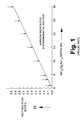
- FIG. 1is a graph showing refractive index of silicon-rich silicon nitride films versus SiH 2 Cl 2 /NH 3 flow rate ratio.
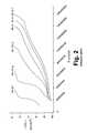
- FIG. 2is a graph showing current density versus applied field for silicon-rich silicon nitride films having different percentages of excess silicon.
- FIG. 3is a graph showing apparent dielectric constant K versus refractive index for both silicon rich nitride (SRN) and silicon rich oxide (SRO).
- FIG. 4is a lumped model illustrating the resistive and inductive losses for an integrated circuit.
- FIG. 5is another model of the electrical behavior for an integrated circuit.
- FIG. 6is the integrated circuit model of FIG. 7 with a lossy decoupling capacitor.
- FIG. 7is a schematic for an on-chip decoupling device.
- FIG. 8illustrates one embodiment of a metal-insulator-silicon (MIS) capacitor formed over an n silicon substrate or an n-well.
- MISmetal-insulator-silicon
- FIG. 9illustrates another embodiment of a MIS capacitor formed over an n silicon substrate or an n-well.
- FIG. 10illustrates another embodiment of a MIS capacitor formed over an p silicon substrate or a p-well.
- FIG. 11illustrates another embodiment of a MIS capacitor formed over an p silicon substrate or a p-well.
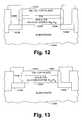
- FIG. 12illustrates one embodiment of a MIS capacitor with a metal top plate.
- FIG. 13illustrates another embodiment of a MIS capacitor with a metal top plate.
- FIG. 14illustrates one embodiment of a metal-insulator-metal (MIM) capacitor with gold nano crystals.
- MIMmetal-insulator-metal
- FIG. 15illustrates another embodiment of a MIM capacitor with silicon nano crystals.
- SRNSilicon-rich nitride
- SROsilicon rich oxide
- FIGS. 1-3described below, are included to elaborate on the characteristics of SRN, including injector SRI.
- FIG. 1is a graph showing refractive index of silicon-rich silicon nitride films versus SiH 2 Cl 2 /NH 3 flow rate ratio (R). This figure is provided herein to illustrate the known relationship between the silicon amount and the refractive index in the film. The graph indicates that the index of refraction increases linearly with increasing silicon content. As such, the index of refraction of the films can be used as an indication of the silicon content of the films.
- FIG. 2is a graph showing current density versus applied field for silicon-rich silicon nitride films having different percentages of excess silicon.
- the current density (J)is represented in amperes/cm 2
- log Jis plotted against the electric field E (volts/cm) for Si 3 N 4 layers having a SiH 2 Cl 2 /NH 3 flow rate ratio R of 0.1, 3, 5, 10, 15 and 31.
- This figureis provided herein to illustrate the known relationship between the amount of silicon and the conductivity of the film.
- Silicon-rich nitride films having an R greater than 10are referred to as an injector medium.
- a silicon-rich Si 3 N 4 (SRN) injectorprovides appreciably enhanced charge conductance without providing significant charge trapping similar to the characteristics of semi-metals.
- Silicon nitride injectorsare preferred over silicon oxide injectors because the two-phase nature of the interface is believed to provide a localized electric field distortion and an associated high current.
- siliconreadily diffuses within silicon oxide and changes the size and geometry of silicon crystals, which disrupts the injection threshold by reducing the localized field distortions.
- silicondoes not readily diffuse within Si 3 N 4 .
- SRNis chemically passive against chemical solutions as well as an effective barrier against n or p type dopant diffusion; that is, against phosphorus or boron respectively.
- FIG. 3is a graph showing apparent dielectric constant K versus refractive index for both silicon rich nitride (SRN) and silicon rich oxide (SRO).
- SRNsilicon rich nitride
- SROsilicon rich oxide
- the SRO and SRO plotted in this graphwere provided using a Low Pressure Chemical Vapor Deposition (LPCVD) process.
- the SROwas fabricated at approximately 680° C., and the fabricated structure included 100 ⁇ oxide and 150 ⁇ SRO.
- the SRNwas fabricated at approximately 770° C., and the fabricated structure included 45 ⁇ oxide and 80 ⁇ SRO.
- the dielectric constant of siliconis around 12. Materials with a higher K than silicon are conventionally termed a high K material, and materials with a lower K than silicon are conventionally termed a low K material.
- Injector SRNare those that have a refractive index of 2.5 or greater and injector SRO are those that have a refractive index of 1.85 or greater. Injector SRN and injector SRO have apparent dielectric constants that are greater than 12. Injector SRI includes both high K SRO and high K SRN.
- injector SRNprovides enhanced charge conductance. Controlling the dispersion and amount of silicon in injector SRN controls the resistivity of the film in which the injector SRN is deposited.
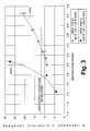
- FIG. 4is a lumped model illustrating the resistive and inductive losses for an integrated circuit.
- the modelincludes a power source 410 and an integrated circuit load 412 .
- the power source 410is represented by both a voltage source 414 and a current source 416 .
- the integrated circuit load 412has a resistive component 418 , an inductive component 420 , and a capacitive component 422 . These are represented in this model as a lumped resistance, a lumped inductor and a lumped capacitor connected in series.
- the lumped resistancecontributes to signal loss as represented by ⁇ V R .
- the lumped inductoralso contributes to signal loss as represented by ⁇ V L .
- FIG. 5is another model of the electrical behavior for an integrated circuit.
- This modelalso includes a power source 510 and an integrated circuit load 512 .
- the power source 510is represented by both a voltage source 514 and a current source 516 .
- the integrated circuit load 512has a resistive component 518 , an inductive component 520 , and a capacitive component 522 .
- the resistive component 518is attributable to the resistance of the chip/substrate.
- the inductive component 520is attributable to the inductance in the substrate and interconnect. In this model, the resistive component and capacitive component are connected in series with each other, and are connected in parallel with the inductive component.
- FIG. 6is the integrated circuit model of FIG. 5 with a lossy decoupling capacitor.
- the lossy decoupling capacitor 624is coupled in parallel with the chip capacitive component 622 of the integrated circuit load 612 .
- the model for the lossy decoupling capacitor 624includes a decoupling capacitor (C DC ) 626 coupled in parallel with a decoupling resistor (R DC ) 628 .
- C DCdecoupling capacitor
- R DCdecoupling resistor
- increasing C DC and R DClowers the resonance impedance (Z RES ) and the resonance frequency (F RES ) and suppresses the V DD oscillation and the V DD noise.
- FIG. 7is a schematic for an on-chip decoupling device according to the present subject matter.
- a substrate 730is provided with isolation regions 732 .
- Control devices 734are formed between isolation regions 732 .
- Each control device 734includes a gate 736 and two diffused regions 738 in the substrate 730 .
- a gate insulator 740separates the gate 736 from the diffused regions 738 .
- An n-well 742is formed between the two control devices 734 .
- a decoupling capacitor plate 744is formed over the n-well, and is separated from the n-well by a capacitor insulator structure 746 .
- This capacitor insulator structure 746provides the characteristics for the lossy decoupling capacitor.
- the fabrication of the insulator structure 746is integrated with the processing of the gate insulator 740 of the control devices 734 .
- R DC and C DCresistive and capacitive component
- One of these manipulated variablesis the K value of the dielectric used in the capacitor insulator structure 746 .
- Other manipulated variables taught by the present subject matterinclude the distribution of nano crystals in the capacitor insulator structure 746 and the composition of the nano crystals. The nano crystals control the resistivity of the high K dielectric.
- FIGS. 8-13illustrate various embodiments of a MIS (metal-insulator-substrate) capacitor.
- the gate oxide for the capacitor insulator structureis a high K dielectric containing tailored amounts of nano crystals. According to various embodiments, these nano crystals are uniformly distributed or dispersed in the high K dielectric.
- the high K dielectricincludes alumina (Al 2 O 3 ).
- silicon or gold nano crystalsare uniformly distributed in Al 2 O 3 by simultaneous sputtering, by implant, by ion-beam deposition or by vapor phase deposition.
- silicon-rich aluminais deposited by chemical vapor deposition (CVD) technique to create a two phase insulator consisting of desired silicon nano crystals uniformly dispersed in Al 2 O 3 .
- the capacitor plateis a silicon plate
- the insulatoris capped with a thin (5 nm, for example) layer of injector SRN which adds an increased resistive component with negligible impact on capacitance. This is because, as was stated above, injector SRN provides appreciably enhanced charge conductance without providing appreciably enhanced charge trapping. Additionally, the injector SRN layer prevents dopant and impurity migration during subsequent high temperature processing.
- the capacitor plateis a metal plate, one embodiment provides a thin layer of titanium nitride (TiN) to provide a diffusion barrier between the insulator and the metal interface.
- TiNtitanium nitride
- One embodimentuses the TiN layer as the top plate of the capacitor.
- the capacitance of the decoupling capacitoris further enhanced by doping transition metals into the high K dielectric material.
- transition metalsinclude, but are not limited to, hafnium (Hf), tantalum (Ta), zirconium (Zr), and praseodymium (Pr).
- a complex high K dielectricis used as the dielectric for the capacitor, or is doped with the high K dielectric for the capacitor.
- barium strontium titanate ((BaSr) TiO 3 )which is also known as BST.
- Ta 2 O 5tantalum pentoxide
- TiO 2titanium dioxide
- TaNtantalum nitride
- ZrO 2zirconium oxide
- Pr 2 O 3praseodymium oxide
- FIG. 8illustrates one embodiment of a MIS capacitor formed over an n silicon substrate or an n-well.
- a layer 850 of gold-doped Al 2 O 3is disposed on the substrate 830 and functions as the capacitor insulator structure 846 .
- Gold-doped Al 2 O 3is Al 2 O 3 doped with gold nano crystals.
- An injector layer 852such as an injector SRN layer, is disposed on the gold-doped Al 2 O 3 .
- the top plate 844 of the capacitoris formed from n+ polysilicon.
- FIG. 9illustrates another embodiment of a MIS capacitor formed over an n silicon substrate or an n-well.
- a layer 950 of silicon-doped Al 2 O 3is disposed on the substrate 930 and functions as the capacitor insulator structure 946 .
- Silicon-doped Al 2 O 3 and Al 2 O 3doped with silicon nano crystals.
- An injector layer 952such as an injector SRN layer, is disposed on the silicon-doped Al 2 O 3 .
- the top plate 944 of the capacitoris formed from n+ polysilicon.
- FIG. 10illustrates another embodiment of a MIS capacitor formed over an p silicon substrate or a p-well.
- a layer 1050 of gold-doped Al 2 O 3is disposed on the substrate 1030 and functions as the capacitor insulator structure 1046 .
- An injector layer 1052such as an injector SRN layer, is disposed on the gold-doped Al 2 O 3 .
- the top plate 1044 of the capacitoris formed from p+ polysilicon.
- FIG. 11illustrates another embodiment of a MIS capacitor formed over an p silicon substrate or a p-well.
- a layer 1150 of silicon-doped Al 2 O 3is disposed on the substrate 1130 and functions as the capacitor insulator structure 1146 .
- An injector layer 1152such as an injector SRN layer, is disposed on the silicon-doped Al 2 O 3 .
- the top plate 1144 of the capacitoris formed from p+ polysilicon.
- FIG. 12illustrates one embodiment of a MIS capacitor with a metal top plate.
- a layer 1250 of gold-doped Al 2 O 3is disposed on the substrate 1230 , and a TiN layer 1254 is disposed thereon.
- a layer 1250 of silicon-doped Al 2 O 3is disposed on the substrate 1230 , and a TiN layer 1254 is disposed thereon.
- the top plate 1244 of the capacitoris formed from a metal.
- FIG. 13illustrates another embodiment of a MIS capacitor with a metal top plate.
- a layer 1350 of gold-doped Al 2 O 3is disposed on the substrate 1330 , and a TiN layer 1354 is disposed thereon.
- a layer 1350 of silicon-doped Al 2 O 3is disposed on the substrate 1330 , and a TiN layer 1354 is disposed thereon.
- the TiN 1354 layerforms the top plate 1344 of the capacitor.
- FIGS. 14-15illustrate various embodiments of a MIM (metal-insulator-metal) capacitor.
- the MIM capacitoris fabricated on top of silicon and is appropriately connected to the Vdd/Gnd nodes, clock trees and active circuits.
- the insulatoris a high K dielectric containing tailored amounts of nano crystals uniformly distributed or dispersed in the high K dielectric. Such insulator is usually fabricated at lower temperature than corresponding MIS options.
- the techniques used for fabricationinclude electron cyclotron resonance-plasma enhanced chemical vapor deposition (ECR-PECVD), atomic layer deposition (ALD), sputtering, E-Beam and Ion-Beam deposition of thin films.
- ECR-PECVDelectron cyclotron resonance-plasma enhanced chemical vapor deposition
- ALDatomic layer deposition
- sputteringE-Beam and Ion-Beam deposition of thin films.
- the high K dielectricincludes Al 2 O 3 .
- ALD aluminumis deposited on top of a tungsten nitride (TiN), a tungsten (W) or tungsten silicide (WSi) electrode and subsequently oxidized in ozone plasma at low temperature.
- silicon or gold nano crystalsare uniformly distributed in Al 2 O 3 by simultaneous sputtering, or by implant, or by vapor phase deposition.
- silicon-rich aluminais deposited by CVD technique to create two phase insulator consisting of desired silicon nano crystals uniformly dispersed in Al 2 O 3 .
- the metal top plateis any metal such as titanium nitride (TiN), copper (Cu) or aluminum (Al).
- the capacitance of the decoupling capacitoris further enhanced by doping transition metals into the high K dielectric such as Al 2 O 3 .
- transition metalsinclude, but are not limited to, hafnium (Hf), tantalum (Ta), zirconium (Zr), praseodymium (Pr).
- a complex high K dielectricis used as the dielectric for the capacitor, or is doped with the high K dielectric for the capacitor.
- One such complex high K dielectricis barium strontium titanate ((BaSr) TiO 3 ) which is also known as BST.
- Ta 2 O 5tantalum pentoxide
- TiO 2titanium dioxide
- TaNtantalum nitride
- ZrO 2zirconium oxide
- Pr 2 O 3praseodymium oxide
- FIG. 14illustrates one embodiment of a MIM capacitor with gold nano crystals.
- a first layer 1462 of TiNis disposed on the bottom metal layer 1460
- a layer 1450 of gold-doped Al 2 O 3is disposed on the first layer of TiN 1462
- a second layer 1444 of TiNis disposed on the layer 1450 of gold-doped Al 2 O 3
- a top plate 1444is formed on the second layer 1444 of TiN.
- the top plateis fabricated from titanium nitride (TiN), copper (Cu), tungsten (W) or aluminum (Al) and the bottom metal layer is fabricated from Cu, W, Al, TiN, or tungsten silicide (WSi).
- FIG. 15illustrates another embodiment of a MIM capacitor with silicon nano crystals.
- a first layer of TiN 1562is disposed on the bottom metal layer 1560
- a layer 1550 of silicon-doped Al 2 O 3is disposed on the first layer 1562 of TiN
- a second layer 1564 of TiNis disposed on the layer 1550 of gold-doped Al 2 O 3
- a top plate 1544is formed on the second layer 1544 of TiN.
- the top plateis fabricated from TiN, Cu, W or Al and the bottom metal layer is fabricated from Cu, W, Al, TiN, or WSi.
- Injector SRNwas provided as an example of an injector medium in the above examples.
- materialsinclude silicon-rich aluminum nitride and SRO.
- Al 2 O 3is not an effective diffusion barrier for certain dopants like phosphorus for an n+ gate.
- the injector media SRN and silicon-rich aluminum nitridefunction as a diffusion barrier for doped polysilicon gates to prevent phosphorous, for example, from diffusing into Al 2 O 3 .
- a diffusion barrieris not needed if a metal gate is used.
- a high K charge blocking mediumis a material that has a K greater than the K of silicon. These materials include oxides, nitrides and silicates of tantalum, titanium, zirconium, hafnium and praseodymium.
- these materialsmay further be doped with complex high K dielectrics such as barium strontium titanate (BST), transition metal, and metal oxides such as tantalum pentoxide (Ta 2 O 5 ), titanium dioxide (TiO 2 ), tantalum nitride (TaN), zirconium oxide (ZrO 2 ), and praseodymium oxide (Pr 2 O 3 ).
- BSTbarium strontium titanate
- metal oxidessuch as tantalum pentoxide (Ta 2 O 5 ), titanium dioxide (TiO 2 ), tantalum nitride (TaN), zirconium oxide (ZrO 2 ), and praseodymium oxide (Pr 2 O 3 ).
- thin films of these materialscan be readily fabricated at near room temperature or at low temperature by several techniques including sputtering, ion beam deposition, and electron cyclotron resonance-plasma enhanced chemical vapor deposition (ECR-PECVD).
- Such an electronic systemincludes a processor or arithmetic/logic unit (ALU), a control unit, a memory device unit and an input/output (I/O) device.
- ALUarithmetic/logic unit
- control unita control unit
- memory device unita memory device unit
- I/Oinput/output
- Such an electronic systemwill have a native set of instructions that specify operations to be performed on data by the processor and other interactions between the processor, the memory device unit and the I/O devices.
- the memory device unitcontains the data plus a stored list of instructions.
- the control unitcoordinates all operations of the processor, the memory device and the I/O devices by continuously cycling through a set of operations that cause instructions to be fetched from the memory device and executed.
- the present subject matterprovides a decoupling capacitor for reducing resonance frequency and impedance in high frequency designs.
- the capacitor insulator structure of the decoupling capacitorincludes a high K dielectric, and nano crystals dispersed through the high K dielectric. The distribution of the nano crystals and the composition of the nano crystals control the resistivity of the high K dielectric.
- the capacitor insulator structureprovides a decoupling capacitor with a high K to provide an effective C DC in a relatively small area and with a built-in controlled R DC to control the resonance impedance and the resonance frequency of an integrated circuit chip. As such, smaller and faster integrate circuit design are achieved.
Landscapes
- Engineering & Computer Science (AREA)
- Chemical & Material Sciences (AREA)
- Crystallography & Structural Chemistry (AREA)
- Physics & Mathematics (AREA)
- Nanotechnology (AREA)
- General Chemical & Material Sciences (AREA)
- Theoretical Computer Science (AREA)
- Chemical Kinetics & Catalysis (AREA)
- Mathematical Physics (AREA)
- Condensed Matter Physics & Semiconductors (AREA)
- General Physics & Mathematics (AREA)
- Manufacturing & Machinery (AREA)
- Computer Hardware Design (AREA)
- Microelectronics & Electronic Packaging (AREA)
- Power Engineering (AREA)
- Semiconductor Integrated Circuits (AREA)
Abstract
Description


Claims (88)
Priority Applications (4)
| Application Number | Priority Date | Filing Date | Title |
|---|---|---|---|
| US09/944,986US6700771B2 (en) | 2001-08-30 | 2001-08-30 | Decoupling capacitor for high frequency noise immunity |
| US10/752,351US6955960B2 (en) | 2001-08-30 | 2004-01-06 | Decoupling capacitor for high frequency noise immunity |
| US11/209,415US20060007633A1 (en) | 2001-08-30 | 2005-08-23 | Decoupling capacitor for high frequency noise immunity |
| US11/209,425US7442633B2 (en) | 2001-08-30 | 2005-08-23 | Decoupling capacitor for high frequency noise immunity |
Applications Claiming Priority (1)
| Application Number | Priority Date | Filing Date | Title |
|---|---|---|---|
| US09/944,986US6700771B2 (en) | 2001-08-30 | 2001-08-30 | Decoupling capacitor for high frequency noise immunity |
Related Child Applications (1)
| Application Number | Title | Priority Date | Filing Date |
|---|---|---|---|
| US10/752,351DivisionUS6955960B2 (en) | 2001-08-30 | 2004-01-06 | Decoupling capacitor for high frequency noise immunity |
Publications (2)
| Publication Number | Publication Date |
|---|---|
| US20030072126A1 US20030072126A1 (en) | 2003-04-17 |
| US6700771B2true US6700771B2 (en) | 2004-03-02 |
Family
ID=25482429
Family Applications (4)
| Application Number | Title | Priority Date | Filing Date |
|---|---|---|---|
| US09/944,986Expired - LifetimeUS6700771B2 (en) | 2001-08-30 | 2001-08-30 | Decoupling capacitor for high frequency noise immunity |
| US10/752,351Expired - Fee RelatedUS6955960B2 (en) | 2001-08-30 | 2004-01-06 | Decoupling capacitor for high frequency noise immunity |
| US11/209,425Expired - Fee RelatedUS7442633B2 (en) | 2001-08-30 | 2005-08-23 | Decoupling capacitor for high frequency noise immunity |
| US11/209,415AbandonedUS20060007633A1 (en) | 2001-08-30 | 2005-08-23 | Decoupling capacitor for high frequency noise immunity |
Family Applications After (3)
| Application Number | Title | Priority Date | Filing Date |
|---|---|---|---|
| US10/752,351Expired - Fee RelatedUS6955960B2 (en) | 2001-08-30 | 2004-01-06 | Decoupling capacitor for high frequency noise immunity |
| US11/209,425Expired - Fee RelatedUS7442633B2 (en) | 2001-08-30 | 2005-08-23 | Decoupling capacitor for high frequency noise immunity |
| US11/209,415AbandonedUS20060007633A1 (en) | 2001-08-30 | 2005-08-23 | Decoupling capacitor for high frequency noise immunity |
Country Status (1)
| Country | Link |
|---|---|
| US (4) | US6700771B2 (en) |
Cited By (56)
| Publication number | Priority date | Publication date | Assignee | Title |
|---|---|---|---|---|
| US20030160277A1 (en)* | 2001-11-09 | 2003-08-28 | Micron Technology, Inc. | Scalable gate and storage dielectric |
| US20040033654A1 (en)* | 2002-08-14 | 2004-02-19 | Osamu Yamagata | Semiconductor device and method of fabricating the same |
| US20040106249A1 (en)* | 2002-12-03 | 2004-06-03 | Hannu Huotari | Method to fabricate dual metal CMOS devices |
| US20040106261A1 (en)* | 2002-12-03 | 2004-06-03 | Asm International N.V. | Method of forming an electrode with adjusted work function |
| US20040104439A1 (en)* | 2002-12-03 | 2004-06-03 | Asm International N.V. | Method of depositing barrier layer from metal gates |
| US20040142528A1 (en)* | 2001-08-30 | 2004-07-22 | Micron Technology, Inc. | Decoupling capacitor for high frequency noise immunity |
| US20050088801A1 (en)* | 2003-10-27 | 2005-04-28 | Taiwan Semiconductor Manufacturing Co., Ltd. | Decoupling capacitor |
| US20060043491A1 (en)* | 2004-08-30 | 2006-03-02 | Taiwan Semiconductor Manufacturing Company, Ltd. | Electrostatic discharge protection device and method for its manufacture |
| US20060102972A1 (en)* | 2004-11-15 | 2006-05-18 | Micron Technology, Inc. | Optoelectronic devices, solar cells, methods of making optoelectronic devices, and methods of making solar cells |
| US7092235B2 (en)* | 2003-09-30 | 2006-08-15 | International Business Machines Corporation | Method for adjusting capacitance of an on-chip capacitor |
| US7113388B2 (en)* | 2002-04-23 | 2006-09-26 | IHP GmbH- Innovations for High Performance | Semiconductor capacitor with praseodymium oxide as dielectric |
| US20060279905A1 (en)* | 2004-03-18 | 2006-12-14 | Nanosys, Inc. | Nanofiber surface based capacitors |
| US20060286734A1 (en)* | 2005-06-17 | 2006-12-21 | Ihp Gmbh - Innovations For High Performance | MIM/MIS structure with praseodymium titanate or praseodymium oxide as insulator material |
| US20070031590A1 (en)* | 2002-03-25 | 2007-02-08 | Fujitsu Limited | Thin film capacitor and method for manufacturing the same |
| US20070132055A1 (en)* | 2005-12-14 | 2007-06-14 | Kim Hwal P | Semiconductor device and manufacturing method thereof |
| US20070138128A1 (en)* | 2005-12-20 | 2007-06-21 | Tdk Corporation | Dielectric device and method of manufacturing the same |
| US20070170553A1 (en)* | 2006-01-20 | 2007-07-26 | International Business Machines Corporation | Methods and apparatuses for creating integrated circuit capacitance from gate array structures |
| WO2006110162A3 (en)* | 2004-09-16 | 2007-09-13 | Nanosys Inc | Artificial dielectrics using nanostructures |
| US20070262794A1 (en)* | 2006-05-10 | 2007-11-15 | Houfei Chen | On-die anti-resonance structure for integrated circuit |
| US20080048231A1 (en)* | 2006-08-28 | 2008-02-28 | Micron Technology, Inc. | Buried decoupling capacitors, devices and systems including same, and methods of fabrication |
| US20080085610A1 (en)* | 2006-10-05 | 2008-04-10 | Asm America, Inc. | Ald of metal silicate films |
| US20090108450A1 (en)* | 2007-10-30 | 2009-04-30 | International Business Machines Corporation | Interconnect structure and method of making same |
| US7563715B2 (en) | 2005-12-05 | 2009-07-21 | Asm International N.V. | Method of producing thin films |
| US20090214767A1 (en)* | 2001-03-06 | 2009-08-27 | Asm America, Inc. | Doping with ald technology |
| US20090309187A1 (en)* | 2005-08-24 | 2009-12-17 | Jae-Hyoung Choi | Semiconductor Device and Method of Fabricating the Same |
| US20100187655A1 (en)* | 2004-08-26 | 2010-07-29 | Jae-Hyoung Choi | Integrated Circuit Capacitors Having Composite Dielectric Layers Therein Containing Crystallization Inhibiting Regions and Methods of Forming Same |
| US20100193955A1 (en)* | 2009-02-02 | 2010-08-05 | Asm America, Inc. | Plasma-enhanced atomic layer deposition of conductive material over dielectric layers |
| US7944020B1 (en)* | 2006-12-22 | 2011-05-17 | Cypress Semiconductor Corporation | Reverse MIM capacitor |
| US20110165405A1 (en)* | 2004-09-16 | 2011-07-07 | Nanosys, Inc. | Continuously variable graded artificial dielectrics using nanostructures |
| US20110298007A1 (en)* | 2008-11-19 | 2011-12-08 | Micron Technology, Inc. | Select devices including an open volume, memory devices and systems including same, and methods for forming same |
| US8395455B1 (en) | 2011-10-14 | 2013-03-12 | United Microelectronics Corp. | Ring oscillator |
| US8421509B1 (en) | 2011-10-25 | 2013-04-16 | United Microelectronics Corp. | Charge pump circuit with low clock feed-through |
| US8493806B1 (en) | 2012-01-03 | 2013-07-23 | United Microelectronics Corporation | Sense-amplifier circuit of memory and calibrating method thereof |
| US8558311B2 (en) | 2004-09-16 | 2013-10-15 | Nanosys, Inc. | Dielectrics using substantially longitudinally oriented insulated conductive wires |
| US8588020B2 (en) | 2011-11-16 | 2013-11-19 | United Microelectronics Corporation | Sense amplifier and method for determining values of voltages on bit-line pair |
| US8610188B2 (en)* | 2011-09-15 | 2013-12-17 | GlobalFoundries, Inc. | Integrated circuit decoupling capacitor arrangement |
| US8643521B1 (en) | 2012-11-28 | 2014-02-04 | United Microelectronics Corp. | Digital-to-analog converter with greater output resistance |
| US8669897B1 (en) | 2012-11-05 | 2014-03-11 | United Microelectronics Corp. | Asynchronous successive approximation register analog-to-digital converter and operating method thereof |
| US8692608B2 (en) | 2011-09-19 | 2014-04-08 | United Microelectronics Corp. | Charge pump system capable of stabilizing an output voltage |
| US8711598B1 (en) | 2012-11-21 | 2014-04-29 | United Microelectronics Corp. | Memory cell and memory cell array using the same |
| US8724404B2 (en) | 2012-10-15 | 2014-05-13 | United Microelectronics Corp. | Memory, supply voltage generation circuit, and operation method of a supply voltage generation circuit used for a memory array |
| US8866536B1 (en) | 2013-11-14 | 2014-10-21 | United Microelectronics Corp. | Process monitoring circuit and method |
| US8873295B2 (en) | 2012-11-27 | 2014-10-28 | United Microelectronics Corporation | Memory and operation method thereof |
| US8917109B2 (en) | 2013-04-03 | 2014-12-23 | United Microelectronics Corporation | Method and device for pulse width estimation |
| US8947911B1 (en) | 2013-11-07 | 2015-02-03 | United Microelectronics Corp. | Method and circuit for optimizing bit line power consumption |
| US8945675B2 (en) | 2008-05-29 | 2015-02-03 | Asm International N.V. | Methods for forming conductive titanium oxide thin films |
| US8953401B2 (en) | 2012-12-07 | 2015-02-10 | United Microelectronics Corp. | Memory device and method for driving memory array thereof |
| US8970197B2 (en) | 2012-08-03 | 2015-03-03 | United Microelectronics Corporation | Voltage regulating circuit configured to have output voltage thereof modulated digitally |
| US9030886B2 (en) | 2012-12-07 | 2015-05-12 | United Microelectronics Corp. | Memory device and driving method thereof |
| US9030221B2 (en) | 2011-09-20 | 2015-05-12 | United Microelectronics Corporation | Circuit structure of test-key and test method thereof |
| US9099430B2 (en) | 2013-12-19 | 2015-08-04 | Intermolecular, Inc. | ZrO-based high K dielectric stack for logic decoupling capacitor or embedded DRAM |
| US9105355B2 (en) | 2013-07-04 | 2015-08-11 | United Microelectronics Corporation | Memory cell array operated with multiple operation voltage |
| US9143143B2 (en) | 2014-01-13 | 2015-09-22 | United Microelectronics Corp. | VCO restart up circuit and method thereof |
| US9523148B1 (en) | 2015-08-25 | 2016-12-20 | Asm Ip Holdings B.V. | Process for deposition of titanium oxynitride for use in integrated circuit fabrication |
| US9540729B1 (en) | 2015-08-25 | 2017-01-10 | Asm Ip Holding B.V. | Deposition of titanium nanolaminates for use in integrated circuit fabrication |
| US10304496B2 (en)* | 2017-03-23 | 2019-05-28 | Toshiba Memory Corporation | Semiconductor device and electronic equipment |
Families Citing this family (42)
| Publication number | Priority date | Publication date | Assignee | Title |
|---|---|---|---|---|
| US6735072B2 (en)* | 2002-04-12 | 2004-05-11 | Sun Microsystems, Inc. | On-chip decoupling capacitors designed for a 0.11 micron and beyond dual gate oxide CMOS technology |
| US7221586B2 (en) | 2002-07-08 | 2007-05-22 | Micron Technology, Inc. | Memory utilizing oxide nanolaminates |
| US6865407B2 (en)* | 2002-07-11 | 2005-03-08 | Optical Sensors, Inc. | Calibration technique for non-invasive medical devices |
| US6888200B2 (en)* | 2002-08-30 | 2005-05-03 | Micron Technology Inc. | One transistor SOI non-volatile random access memory cell |
| US7042027B2 (en)* | 2002-08-30 | 2006-05-09 | Micron Technology, Inc. | Gated lateral thyristor-based random access memory cell (GLTRAM) |
| US6917078B2 (en) | 2002-08-30 | 2005-07-12 | Micron Technology Inc. | One transistor SOI non-volatile random access memory cell |
| US6903969B2 (en)* | 2002-08-30 | 2005-06-07 | Micron Technology Inc. | One-device non-volatile random access memory cell |
| US20040077142A1 (en)* | 2002-10-17 | 2004-04-22 | Taiwan Semiconductor Manufacturing Co., Ltd. | Atomic layer deposition and plasma treatment method for forming microelectronic capacitor structure with aluminum oxide containing dual dielectric layer |
| US8125003B2 (en)* | 2003-07-02 | 2012-02-28 | Micron Technology, Inc. | High-performance one-transistor memory cell |
| US7078742B2 (en)* | 2003-07-25 | 2006-07-18 | Taiwan Semiconductor Manufacturing Co., Ltd. | Strained-channel semiconductor structure and method of fabricating the same |
| US6936881B2 (en)* | 2003-07-25 | 2005-08-30 | Taiwan Semiconductor Manufacturing Company, Ltd. | Capacitor that includes high permittivity capacitor dielectric |
| US7888201B2 (en) | 2003-11-04 | 2011-02-15 | Taiwan Semiconductor Manufacturing Company, Ltd. | Semiconductor-on-insulator SRAM configured using partially-depleted and fully-depleted transistors |
| US7816722B2 (en)* | 2004-02-04 | 2010-10-19 | Hewlett-Packard Development Company, L.P. | Memory array |
| US7145186B2 (en) | 2004-08-24 | 2006-12-05 | Micron Technology, Inc. | Memory cell with trenched gated thyristor |
| US7388248B2 (en)* | 2004-09-01 | 2008-06-17 | Micron Technology, Inc. | Dielectric relaxation memory |
| US7309895B2 (en) | 2005-01-25 | 2007-12-18 | Hewlett-Packard Development Company, L.P. | Semiconductor device |
| US7361950B2 (en)* | 2005-09-12 | 2008-04-22 | International Business Machines Corporation | Integration of a MIM capacitor with a plate formed in a well region and with a high-k dielectric |
| KR20070035341A (en)* | 2005-09-27 | 2007-03-30 | 삼성전자주식회사 | Light-Emitting Device Containing Semiconductor Nanocrystalline Layer Filling Gaps and Manufacturing Method Thereof |
| US7608913B2 (en)* | 2006-02-23 | 2009-10-27 | Freescale Semiconductor, Inc. | Noise isolation between circuit blocks in an integrated circuit chip |
| US20070222027A1 (en)* | 2006-03-27 | 2007-09-27 | Yang Jeong-Hwan | Electronic fuse elements with constricted neck regions that support reliable fuse blowing |
| US20080149611A1 (en)* | 2006-12-22 | 2008-06-26 | Roth Michael W | Wire feeder packaging and transport system |
| KR100968427B1 (en)* | 2007-05-07 | 2010-07-07 | 주식회사 하이닉스반도체 | Capacitor including a dielectric film doped with an impurity and a method of manufacturing the same |
| EP2319060A1 (en)* | 2008-08-26 | 2011-05-11 | Nxp B.V. | A capacitor and a method of manufacturing the same |
| US8436408B2 (en)* | 2008-09-17 | 2013-05-07 | Taiwan Semiconductor Manufacturing Co., Ltd. | Semiconductor device with decoupling capacitor design |
| CA2748655A1 (en)* | 2009-01-16 | 2010-07-22 | The Board Of Trustees Of The Leland Stanford Junior University | Quantum dot ultracapacitor and electron battery |
| JP2012523117A (en)* | 2009-04-01 | 2012-09-27 | ボード オブ トラスティーズ オブ ザ レランド スタンフォード ジュニア ユニバーシティ | All-electron battery with electrodes of increased area |
| CN101996951B (en)* | 2009-08-20 | 2013-09-11 | 中芯国际集成电路制造(上海)有限公司 | Nonvolatile memory structure and forming method thereof |
| US8542475B2 (en)* | 2009-10-09 | 2013-09-24 | The Penn State Research Foundation | Self healing high energy glass capacitors |
| CN102097383B (en)* | 2009-12-15 | 2013-06-19 | 中芯国际集成电路制造(上海)有限公司 | Method for manufacturing double-bit flash memory |
| CN102097490A (en)* | 2009-12-15 | 2011-06-15 | 中芯国际集成电路制造(上海)有限公司 | Method for manufacturing double-bit flash memory |
| CN102110657A (en)* | 2009-12-29 | 2011-06-29 | 中芯国际集成电路制造(上海)有限公司 | Method for producing double-bit flash memory |
| CN102110658B (en)* | 2009-12-29 | 2013-07-17 | 中芯国际集成电路制造(上海)有限公司 | Method for fabricating dibit flash memory |
| US9275801B2 (en)* | 2010-03-19 | 2016-03-01 | Cardiac Pacemakers, Inc. | Systems and methods for enhanced dielectric properties for electrolytic capacitors |
| US8767404B2 (en) | 2011-07-01 | 2014-07-01 | Altera Corporation | Decoupling capacitor circuitry |
| JP2014144881A (en)* | 2013-01-28 | 2014-08-14 | Mitsubishi Materials Corp | Dielectric thin film-forming composition and method of forming dielectric thin film using the same |
| US9231046B2 (en) | 2013-03-15 | 2016-01-05 | Globalfoundries Inc. | Capacitor using barrier layer metallurgy |
| KR102464065B1 (en)* | 2016-01-27 | 2022-11-08 | 에스케이하이닉스 주식회사 | switching device and method of fabricating the same, and resistive random access memory having the switching device as selection device |
| US10418364B2 (en)* | 2016-08-31 | 2019-09-17 | Globalfoundries Inc. | Semiconductor device structure with self-aligned capacitor device |
| DE102019102657A1 (en)* | 2019-02-04 | 2020-08-06 | Bayerische Motoren Werke Aktiengesellschaft | Radio-frequency permeable component and method for producing the same |
| KR102792553B1 (en) | 2020-02-26 | 2025-04-08 | 삼성전자주식회사 | Capacitor, semiconductor device inclduing the same, method of fabricating capacitor |
| US20230317772A1 (en)* | 2022-04-01 | 2023-10-05 | Macom Technology Solutions Holdings, Inc. | Selective etching of silicon layers in a semiconductor device |
| US20250105813A1 (en)* | 2023-09-21 | 2025-03-27 | Macom Technology Solutions Holdings, Inc. | Broadband decoupling network |
Citations (2)
| Publication number | Priority date | Publication date | Assignee | Title |
|---|---|---|---|---|
| US5587870A (en)* | 1992-09-17 | 1996-12-24 | Research Foundation Of State University Of New York | Nanocrystalline layer thin film capacitors |
| US20020000593A1 (en)* | 2000-06-27 | 2002-01-03 | Akira Nishiyama | Semiconductor device and method of manufacturing the same |
Family Cites Families (20)
| Publication number | Priority date | Publication date | Assignee | Title |
|---|---|---|---|---|
| US4333808A (en)* | 1979-10-30 | 1982-06-08 | International Business Machines Corporation | Method for manufacture of ultra-thin film capacitor |
| US4952273A (en)* | 1988-09-21 | 1990-08-28 | Microscience, Inc. | Plasma generation in electron cyclotron resonance |
| US5366586A (en)* | 1992-02-03 | 1994-11-22 | Nec Corporation | Plasma formation using electron cyclotron resonance and method for processing substrate by using the same |
| GB9323498D0 (en)* | 1993-11-15 | 1994-01-05 | Isis Innovation | Making particles of uniform size |
| US5656834A (en)* | 1994-09-19 | 1997-08-12 | Philips Electronics North America Corporation | IC standard cell designed with embedded capacitors |
| US5714766A (en) | 1995-09-29 | 1998-02-03 | International Business Machines Corporation | Nano-structure memory device |
| US5620909A (en)* | 1995-12-04 | 1997-04-15 | Lucent Technologies Inc. | Method of depositing thin passivating film on microminiature semiconductor devices |
| US6159620A (en)* | 1997-03-31 | 2000-12-12 | The Regents Of The University Of California | Single-electron solid state electronic device |
| US6282079B1 (en)* | 1998-11-30 | 2001-08-28 | Kyocera Corporation | Capacitor |
| US6245617B1 (en)* | 1999-05-06 | 2001-06-12 | United Microelectronics Corp. | Method of fabricating dielectric layer |
| KR100705926B1 (en)* | 1999-12-22 | 2007-04-11 | 주식회사 하이닉스반도체 | Capacitor Manufacturing Method of Semiconductor Device |
| US6475854B2 (en) | 1999-12-30 | 2002-11-05 | Applied Materials, Inc. | Method of forming metal electrodes |
| US6418031B1 (en)* | 2000-05-01 | 2002-07-09 | International Business Machines Corporation | Method and means for decoupling a printed circuit board |
| US6689220B1 (en)* | 2000-11-22 | 2004-02-10 | Simplus Systems Corporation | Plasma enhanced pulsed layer deposition |
| US7192827B2 (en)* | 2001-01-05 | 2007-03-20 | Micron Technology, Inc. | Methods of forming capacitor structures |
| US6362012B1 (en)* | 2001-03-05 | 2002-03-26 | Taiwan Semiconductor Manufacturing Company | Structure of merged vertical capacitor inside spiral conductor for RF and mixed-signal applications |
| US6518106B2 (en)* | 2001-05-26 | 2003-02-11 | Motorola, Inc. | Semiconductor device and a method therefor |
| US6511873B2 (en)* | 2001-06-15 | 2003-01-28 | International Business Machines Corporation | High-dielectric constant insulators for FEOL capacitors |
| US6700771B2 (en)* | 2001-08-30 | 2004-03-02 | Micron Technology, Inc. | Decoupling capacitor for high frequency noise immunity |
| US6860818B2 (en)* | 2002-06-17 | 2005-03-01 | Callaway Golf Company | Golf club head with peripheral weighting |
- 2001
- 2001-08-30USUS09/944,986patent/US6700771B2/ennot_activeExpired - Lifetime
- 2004
- 2004-01-06USUS10/752,351patent/US6955960B2/ennot_activeExpired - Fee Related
- 2005
- 2005-08-23USUS11/209,425patent/US7442633B2/ennot_activeExpired - Fee Related
- 2005-08-23USUS11/209,415patent/US20060007633A1/ennot_activeAbandoned
Patent Citations (2)
| Publication number | Priority date | Publication date | Assignee | Title |
|---|---|---|---|---|
| US5587870A (en)* | 1992-09-17 | 1996-12-24 | Research Foundation Of State University Of New York | Nanocrystalline layer thin film capacitors |
| US20020000593A1 (en)* | 2000-06-27 | 2002-01-03 | Akira Nishiyama | Semiconductor device and method of manufacturing the same |
Non-Patent Citations (3)
| Title |
|---|
| Bhattacharyya, A.,et al. ,"Physical & Electrical Characteristics of LPCVD Silicon Rich Nitride", ECS Technical Digest, vol. 131, No. 11, 691 RNP, New Orleans, (1984),469C. |
| Lee, J.,"Effect of Polysilicon Gate on the Flatband Voltage Shift and Mobility Degradation for ALD-AI203 Gate Dielectric", IEDM, (2000),pp. 645-648. |
| Manchanda, L.,et al. ,"Si-Doped Aluminates for High Temperature Metal-Gate CMOS: Zr-Al-Si-O, A Novel Gate Dielectric for Low Power Application", IEDM Technical Digest, San Francisco, Dec. 10-13, 2000, (2000),23-26. |
Cited By (113)
| Publication number | Priority date | Publication date | Assignee | Title |
|---|---|---|---|---|
| US9139906B2 (en) | 2001-03-06 | 2015-09-22 | Asm America, Inc. | Doping with ALD technology |
| US20090214767A1 (en)* | 2001-03-06 | 2009-08-27 | Asm America, Inc. | Doping with ald technology |
| US6955960B2 (en)* | 2001-08-30 | 2005-10-18 | Micron Technology, Inc. | Decoupling capacitor for high frequency noise immunity |
| US7442633B2 (en) | 2001-08-30 | 2008-10-28 | Micron Technology, Inc. | Decoupling capacitor for high frequency noise immunity |
| US20040142528A1 (en)* | 2001-08-30 | 2004-07-22 | Micron Technology, Inc. | Decoupling capacitor for high frequency noise immunity |
| US20060007633A1 (en)* | 2001-08-30 | 2006-01-12 | Micron Technology, Inc. | Decoupling capacitor for high frequency noise immunity |
| US20060008978A1 (en)* | 2001-08-30 | 2006-01-12 | Micron Technology, Inc. | Decoupling capacitor for high frequency noise immunity |
| US7528043B2 (en) | 2001-11-09 | 2009-05-05 | Micron Technology, Inc. | Scalable gate and storage dielectric |
| US20030160277A1 (en)* | 2001-11-09 | 2003-08-28 | Micron Technology, Inc. | Scalable gate and storage dielectric |
| US20060084214A1 (en)* | 2001-11-09 | 2006-04-20 | Micron Technology, Inc. | Scalable gate and storage dielectric |
| US6998667B2 (en)* | 2001-11-09 | 2006-02-14 | Micron Technology, Inc. | Scalable gate and storage dielectric |
| US20070031590A1 (en)* | 2002-03-25 | 2007-02-08 | Fujitsu Limited | Thin film capacitor and method for manufacturing the same |
| US7349195B2 (en)* | 2002-03-25 | 2008-03-25 | Fujitsu Limited | Thin film capacitor and method for manufacturing the same |
| US7113388B2 (en)* | 2002-04-23 | 2006-09-26 | IHP GmbH- Innovations for High Performance | Semiconductor capacitor with praseodymium oxide as dielectric |
| US20040033654A1 (en)* | 2002-08-14 | 2004-02-19 | Osamu Yamagata | Semiconductor device and method of fabricating the same |
| US6858524B2 (en)* | 2002-12-03 | 2005-02-22 | Asm International, Nv | Method of depositing barrier layer for metal gates |
| US20050104112A1 (en)* | 2002-12-03 | 2005-05-19 | Suvi Haukka | Method of depositing barrier layer from metal gates |
| US20040106249A1 (en)* | 2002-12-03 | 2004-06-03 | Hannu Huotari | Method to fabricate dual metal CMOS devices |
| US20040106261A1 (en)* | 2002-12-03 | 2004-06-03 | Asm International N.V. | Method of forming an electrode with adjusted work function |
| US7045406B2 (en) | 2002-12-03 | 2006-05-16 | Asm International, N.V. | Method of forming an electrode with adjusted work function |
| US20040104439A1 (en)* | 2002-12-03 | 2004-06-03 | Asm International N.V. | Method of depositing barrier layer from metal gates |
| US7122414B2 (en) | 2002-12-03 | 2006-10-17 | Asm International, Inc. | Method to fabricate dual metal CMOS devices |
| US7092235B2 (en)* | 2003-09-30 | 2006-08-15 | International Business Machines Corporation | Method for adjusting capacitance of an on-chip capacitor |
| US7247543B2 (en) | 2003-10-27 | 2007-07-24 | Taiwan Semiconductor Manufacturing Company, Ltd. | Decoupling capacitor |
| US6937457B2 (en)* | 2003-10-27 | 2005-08-30 | Taiwan Semiconductor Manufacturing Company, Ltd. | Decoupling capacitor |
| US20050088801A1 (en)* | 2003-10-27 | 2005-04-28 | Taiwan Semiconductor Manufacturing Co., Ltd. | Decoupling capacitor |
| US20050176195A1 (en)* | 2003-10-27 | 2005-08-11 | Taiwan Semiconductor Manufacturing Company, Ltd. | Decoupling capacitor |
| US20060279905A1 (en)* | 2004-03-18 | 2006-12-14 | Nanosys, Inc. | Nanofiber surface based capacitors |
| US7295419B2 (en) | 2004-03-18 | 2007-11-13 | Nanosys, Inc. | Nanofiber surface based capacitors |
| US8344439B2 (en) | 2004-08-26 | 2013-01-01 | Samsung Electronics Co., Ltd. | Integrated circuit capacitors having composite dielectric layers therein containing crystallization inhibiting regions and methods of forming same |
| US20100187655A1 (en)* | 2004-08-26 | 2010-07-29 | Jae-Hyoung Choi | Integrated Circuit Capacitors Having Composite Dielectric Layers Therein Containing Crystallization Inhibiting Regions and Methods of Forming Same |
| US7973352B2 (en) | 2004-08-26 | 2011-07-05 | Samsung Electronics Co., Ltd. | Capacitors having composite dielectric layers containing crystallization inhibiting regions |
| US9059330B2 (en) | 2004-08-26 | 2015-06-16 | Samsung Electronics Co., Ltd. | Methods of forming integrated circuit capacitors having composite dielectric layers therein containing crystallization inhibiting regions |
| US20060043491A1 (en)* | 2004-08-30 | 2006-03-02 | Taiwan Semiconductor Manufacturing Company, Ltd. | Electrostatic discharge protection device and method for its manufacture |
| US7420250B2 (en) | 2004-08-30 | 2008-09-02 | Taiwan Semiconductor Manufacturing Company, Ltd. | Electrostatic discharge protection device having light doped regions |
| US20070296032A1 (en)* | 2004-09-16 | 2007-12-27 | Nanosys, Inc. | Artificial dielectrics using nanostructures |
| US7365395B2 (en)* | 2004-09-16 | 2008-04-29 | Nanosys, Inc. | Artificial dielectrics using nanostructures |
| US8089152B2 (en) | 2004-09-16 | 2012-01-03 | Nanosys, Inc. | Continuously variable graded artificial dielectrics using nanostructures |
| WO2006110162A3 (en)* | 2004-09-16 | 2007-09-13 | Nanosys Inc | Artificial dielectrics using nanostructures |
| US8558311B2 (en) | 2004-09-16 | 2013-10-15 | Nanosys, Inc. | Dielectrics using substantially longitudinally oriented insulated conductive wires |
| US20110165405A1 (en)* | 2004-09-16 | 2011-07-07 | Nanosys, Inc. | Continuously variable graded artificial dielectrics using nanostructures |
| US7723166B2 (en) | 2004-11-15 | 2010-05-25 | Micron Technology, Inc. | Optoelectronic devices and solar cells |
| US20070194399A1 (en)* | 2004-11-15 | 2007-08-23 | Arup Bhattacharyya | Optoelectronic devices and solar cells |
| US20060102972A1 (en)* | 2004-11-15 | 2006-05-18 | Micron Technology, Inc. | Optoelectronic devices, solar cells, methods of making optoelectronic devices, and methods of making solar cells |
| US20100193032A1 (en)* | 2004-11-15 | 2010-08-05 | Micron Technology, Inc. | Solar Cell Systems |
| US8319272B2 (en) | 2004-11-15 | 2012-11-27 | Micron Technology Inc. | Solar cell systems |
| US7687402B2 (en) | 2004-11-15 | 2010-03-30 | Micron Technology, Inc. | Methods of making optoelectronic devices, and methods of making solar cells |
| US20060286734A1 (en)* | 2005-06-17 | 2006-12-21 | Ihp Gmbh - Innovations For High Performance | MIM/MIS structure with praseodymium titanate or praseodymium oxide as insulator material |
| US20090309187A1 (en)* | 2005-08-24 | 2009-12-17 | Jae-Hyoung Choi | Semiconductor Device and Method of Fabricating the Same |
| US7563715B2 (en) | 2005-12-05 | 2009-07-21 | Asm International N.V. | Method of producing thin films |
| US20070132055A1 (en)* | 2005-12-14 | 2007-06-14 | Kim Hwal P | Semiconductor device and manufacturing method thereof |
| US20070138128A1 (en)* | 2005-12-20 | 2007-06-21 | Tdk Corporation | Dielectric device and method of manufacturing the same |
| US8468693B2 (en) | 2005-12-20 | 2013-06-25 | Tdk Corporation | Dielectric device and method of manufacturing the same |
| US7808769B2 (en)* | 2005-12-20 | 2010-10-05 | Tdk Corporation | Dielectric device and method of manufacturing the same |
| US20100323097A1 (en)* | 2005-12-20 | 2010-12-23 | Tdk Corporation | Dielectric device and method of manufacturing the same |
| US8188516B2 (en) | 2006-01-20 | 2012-05-29 | International Business Machines Corporation | Creating integrated circuit capacitance from gate array structures |
| US7728362B2 (en) | 2006-01-20 | 2010-06-01 | International Business Machines Corporation | Creating integrated circuit capacitance from gate array structures |
| US8298888B2 (en) | 2006-01-20 | 2012-10-30 | International Business Machines Corporation | Creating integrated circuit capacitance from gate array structures |
| US20070170553A1 (en)* | 2006-01-20 | 2007-07-26 | International Business Machines Corporation | Methods and apparatuses for creating integrated circuit capacitance from gate array structures |
| US20100073972A1 (en)* | 2006-05-10 | 2010-03-25 | Houfei Chen | On-die anti-resonance structure for integrated circuit |
| US7633773B2 (en)* | 2006-05-10 | 2009-12-15 | Micron Technology, Inc. | On-die anti-resonance structure for integrated circuit |
| US8023293B2 (en) | 2006-05-10 | 2011-09-20 | Micron Technology, Inc. | On-die anti-resonance structure for integrated circuit |
| US8243479B2 (en) | 2006-05-10 | 2012-08-14 | Micron Technology, Inc. | On-die anti-resonance structure for integrated circuit |
| US20070262794A1 (en)* | 2006-05-10 | 2007-11-15 | Houfei Chen | On-die anti-resonance structure for integrated circuit |
| US20110092045A1 (en)* | 2006-08-28 | 2011-04-21 | Badih El-Kareh | Buried decoupling capacitors, devices and systems including same, and methods of fabrication |
| US8114753B2 (en) | 2006-08-28 | 2012-02-14 | Micron Technology, Inc. | Buried decoupling capacitors, devices and systems including same, and methods of fabrication |
| US8618633B2 (en) | 2006-08-28 | 2013-12-31 | Micron Technology, Inc. | Semiconductor-on-insulator apparatus, device and system with buried decoupling capacitors |
| US7880267B2 (en) | 2006-08-28 | 2011-02-01 | Micron Technology, Inc. | Buried decoupling capacitors, devices and systems including same, and methods of fabrication |
| US20080048231A1 (en)* | 2006-08-28 | 2008-02-28 | Micron Technology, Inc. | Buried decoupling capacitors, devices and systems including same, and methods of fabrication |
| US7972977B2 (en) | 2006-10-05 | 2011-07-05 | Asm America, Inc. | ALD of metal silicate films |
| US8563444B2 (en) | 2006-10-05 | 2013-10-22 | Asm America, Inc. | ALD of metal silicate films |
| US20080085610A1 (en)* | 2006-10-05 | 2008-04-10 | Asm America, Inc. | Ald of metal silicate films |
| US7944020B1 (en)* | 2006-12-22 | 2011-05-17 | Cypress Semiconductor Corporation | Reverse MIM capacitor |
| US8607424B1 (en) | 2006-12-22 | 2013-12-17 | Cypress Semiconductor Corp. | Reverse MIM capacitor |
| US20090108450A1 (en)* | 2007-10-30 | 2009-04-30 | International Business Machines Corporation | Interconnect structure and method of making same |
| US8945675B2 (en) | 2008-05-29 | 2015-02-03 | Asm International N.V. | Methods for forming conductive titanium oxide thin films |
| US9646820B2 (en) | 2008-05-29 | 2017-05-09 | Asm International N.V. | Methods for forming conductive titanium oxide thin films |
| US8541770B2 (en)* | 2008-11-19 | 2013-09-24 | Micron Technology, Inc. | Select devices including an open volume, memory devices and systems including same, and methods for forming same |
| US8957403B2 (en) | 2008-11-19 | 2015-02-17 | Micron Technology, Inc. | Select devices including an open volume, and related methods, memory devices, and electronic systems |
| US20110298007A1 (en)* | 2008-11-19 | 2011-12-08 | Micron Technology, Inc. | Select devices including an open volume, memory devices and systems including same, and methods for forming same |
| US9466574B2 (en) | 2009-02-02 | 2016-10-11 | Asm America, Inc. | Plasma-enhanced atomic layer deposition of conductive material over dielectric layers |
| US8557702B2 (en) | 2009-02-02 | 2013-10-15 | Asm America, Inc. | Plasma-enhanced atomic layers deposition of conductive material over dielectric layers |
| US20100193955A1 (en)* | 2009-02-02 | 2010-08-05 | Asm America, Inc. | Plasma-enhanced atomic layer deposition of conductive material over dielectric layers |
| US8610188B2 (en)* | 2011-09-15 | 2013-12-17 | GlobalFoundries, Inc. | Integrated circuit decoupling capacitor arrangement |
| US8692608B2 (en) | 2011-09-19 | 2014-04-08 | United Microelectronics Corp. | Charge pump system capable of stabilizing an output voltage |
| US9030221B2 (en) | 2011-09-20 | 2015-05-12 | United Microelectronics Corporation | Circuit structure of test-key and test method thereof |
| US8395455B1 (en) | 2011-10-14 | 2013-03-12 | United Microelectronics Corp. | Ring oscillator |
| US8421509B1 (en) | 2011-10-25 | 2013-04-16 | United Microelectronics Corp. | Charge pump circuit with low clock feed-through |
| US8588020B2 (en) | 2011-11-16 | 2013-11-19 | United Microelectronics Corporation | Sense amplifier and method for determining values of voltages on bit-line pair |
| US8493806B1 (en) | 2012-01-03 | 2013-07-23 | United Microelectronics Corporation | Sense-amplifier circuit of memory and calibrating method thereof |
| US8970197B2 (en) | 2012-08-03 | 2015-03-03 | United Microelectronics Corporation | Voltage regulating circuit configured to have output voltage thereof modulated digitally |
| US8724404B2 (en) | 2012-10-15 | 2014-05-13 | United Microelectronics Corp. | Memory, supply voltage generation circuit, and operation method of a supply voltage generation circuit used for a memory array |
| US8804440B1 (en) | 2012-10-15 | 2014-08-12 | United Microelectronics Corporation | Memory for a voltage regulator circuit |
| US8767485B1 (en) | 2012-10-15 | 2014-07-01 | United Microelectronics Corp. | Operation method of a supply voltage generation circuit used for a memory array |
| US8669897B1 (en) | 2012-11-05 | 2014-03-11 | United Microelectronics Corp. | Asynchronous successive approximation register analog-to-digital converter and operating method thereof |
| US8711598B1 (en) | 2012-11-21 | 2014-04-29 | United Microelectronics Corp. | Memory cell and memory cell array using the same |
| US8873295B2 (en) | 2012-11-27 | 2014-10-28 | United Microelectronics Corporation | Memory and operation method thereof |
| US8643521B1 (en) | 2012-11-28 | 2014-02-04 | United Microelectronics Corp. | Digital-to-analog converter with greater output resistance |
| US8953401B2 (en) | 2012-12-07 | 2015-02-10 | United Microelectronics Corp. | Memory device and method for driving memory array thereof |
| US9030886B2 (en) | 2012-12-07 | 2015-05-12 | United Microelectronics Corp. | Memory device and driving method thereof |
| US8917109B2 (en) | 2013-04-03 | 2014-12-23 | United Microelectronics Corporation | Method and device for pulse width estimation |
| US9105355B2 (en) | 2013-07-04 | 2015-08-11 | United Microelectronics Corporation | Memory cell array operated with multiple operation voltage |
| US8947911B1 (en) | 2013-11-07 | 2015-02-03 | United Microelectronics Corp. | Method and circuit for optimizing bit line power consumption |
| US8866536B1 (en) | 2013-11-14 | 2014-10-21 | United Microelectronics Corp. | Process monitoring circuit and method |
| US9099430B2 (en) | 2013-12-19 | 2015-08-04 | Intermolecular, Inc. | ZrO-based high K dielectric stack for logic decoupling capacitor or embedded DRAM |
| US9143143B2 (en) | 2014-01-13 | 2015-09-22 | United Microelectronics Corp. | VCO restart up circuit and method thereof |
| US9523148B1 (en) | 2015-08-25 | 2016-12-20 | Asm Ip Holdings B.V. | Process for deposition of titanium oxynitride for use in integrated circuit fabrication |
| US9540729B1 (en) | 2015-08-25 | 2017-01-10 | Asm Ip Holding B.V. | Deposition of titanium nanolaminates for use in integrated circuit fabrication |
| US10002755B2 (en) | 2015-08-25 | 2018-06-19 | Asm Ip Holding B.V. | Process for deposition of titanium oxynitride for use in integrated circuit fabrication |
| US10460928B2 (en) | 2015-08-25 | 2019-10-29 | Asm Ip Holding B.V. | Process for deposition of titanium oxynitride for use in integrated circuit fabrication |
| US10546744B2 (en) | 2015-08-25 | 2020-01-28 | Asm Ip Holding B.V. | Process for deposition of titanium oxynitride for use in integrated circuit fabrication |
| US11195712B2 (en) | 2015-08-25 | 2021-12-07 | Asm Ip Holding B.V. | Process for deposition of titanium oxynitride for use in integrated circuit fabrication |
| US10304496B2 (en)* | 2017-03-23 | 2019-05-28 | Toshiba Memory Corporation | Semiconductor device and electronic equipment |
Also Published As
| Publication number | Publication date |
|---|---|
| US20030072126A1 (en) | 2003-04-17 |
| US6955960B2 (en) | 2005-10-18 |
| US20040142528A1 (en) | 2004-07-22 |
| US7442633B2 (en) | 2008-10-28 |
| US20060008978A1 (en) | 2006-01-12 |
| US20060007633A1 (en) | 2006-01-12 |
Similar Documents
| Publication | Publication Date | Title |
|---|---|---|
| US6700771B2 (en) | Decoupling capacitor for high frequency noise immunity | |
| KR102715042B1 (en) | Capacitor and electronic device including the semiconductor device | |
| TWI557866B (en) | Composite circuit components and capacitors using CMOS-compatible antiferroelectric high dielectric materials | |
| US6713846B1 (en) | Multilayer high κ dielectric films | |
| JP3207110B2 (en) | Capacitor and method of forming the same | |
| US20030096473A1 (en) | Method for making metal capacitors with low leakage currents for mixed-signal devices | |
| US20040018747A1 (en) | Deposition method of a dielectric layer | |
| US20210359135A1 (en) | Ferroelectric mfm inductor and related circuits | |
| JPH06350029A (en) | Microelectronic circuit structure and its manufacturing method | |
| US11889701B2 (en) | Memory cell including polarization retention member(s) including antiferroelectric layer over ferroelectric layer | |
| CN102187440A (en) | Capacitor, dielectric structure and method of forming dielectric structure | |
| US20230320078A1 (en) | Capacitor, method of controlling the same, and transistor including the same | |
| KR100947064B1 (en) | Capacitor of semiconductor device and memory device having same | |
| US6235594B1 (en) | Methods of fabricating an integrated circuit device with composite oxide dielectric | |
| Tu et al. | Characterization and comparison of high-k metal-insulator-metal (MiM) capacitors in 0.13/spl mu/m Cu BEOL for mixed-mode and RF applications | |
| US20050132549A1 (en) | Method for making metal capacitors with low leakage currents for mixed-signal devices | |
| US20040061157A1 (en) | Semiconductor device | |
| US6285052B1 (en) | Integrated capacitor | |
| DE102005051573B4 (en) | MIM / MIS structure with praseodymium titanate as insulator material | |
| US6608747B1 (en) | Variable-capacitance device and voltage-controlled oscillator | |
| US6700145B1 (en) | Capacitor with high charge storage capacity | |
| US9966425B1 (en) | Method for fabricating a MIM capacitor | |
| Jones Jr et al. | High-permittivity lead-based perovskite dielectrics for DRAM applications | |
| DE102014212483A1 (en) | Complex circuit element and capacitor with CMOS-compatible high-k antiferroelectric materials | |
| KR19990053224A (en) | Capacitor of semiconductor memory device and manufacturing method thereof |
Legal Events
| Date | Code | Title | Description |
|---|---|---|---|
| AS | Assignment | Owner name:MICRON TECHNOLOGY, INC., IDAHO Free format text:ASSIGNMENT OF ASSIGNORS INTEREST;ASSIGNOR:BHATTACHARYYA, ARUP;REEL/FRAME:012144/0381 Effective date:20010829 | |
| FEPP | Fee payment procedure | Free format text:PAYOR NUMBER ASSIGNED (ORIGINAL EVENT CODE: ASPN); ENTITY STATUS OF PATENT OWNER: LARGE ENTITY | |
| STCF | Information on status: patent grant | Free format text:PATENTED CASE | |
| CC | Certificate of correction | ||
| FPAY | Fee payment | Year of fee payment:4 | |
| FPAY | Fee payment | Year of fee payment:8 | |
| FPAY | Fee payment | Year of fee payment:12 | |
| AS | Assignment | Owner name:U.S. BANK NATIONAL ASSOCIATION, AS COLLATERAL AGENT, CALIFORNIA Free format text:SECURITY INTEREST;ASSIGNOR:MICRON TECHNOLOGY, INC.;REEL/FRAME:038669/0001 Effective date:20160426 Owner name:U.S. BANK NATIONAL ASSOCIATION, AS COLLATERAL AGEN Free format text:SECURITY INTEREST;ASSIGNOR:MICRON TECHNOLOGY, INC.;REEL/FRAME:038669/0001 Effective date:20160426 | |
| AS | Assignment | Owner name:MORGAN STANLEY SENIOR FUNDING, INC., AS COLLATERAL AGENT, MARYLAND Free format text:PATENT SECURITY AGREEMENT;ASSIGNOR:MICRON TECHNOLOGY, INC.;REEL/FRAME:038954/0001 Effective date:20160426 Owner name:MORGAN STANLEY SENIOR FUNDING, INC., AS COLLATERAL Free format text:PATENT SECURITY AGREEMENT;ASSIGNOR:MICRON TECHNOLOGY, INC.;REEL/FRAME:038954/0001 Effective date:20160426 | |
| AS | Assignment | Owner name:U.S. BANK NATIONAL ASSOCIATION, AS COLLATERAL AGENT, CALIFORNIA Free format text:CORRECTIVE ASSIGNMENT TO CORRECT THE REPLACE ERRONEOUSLY FILED PATENT #7358718 WITH THE CORRECT PATENT #7358178 PREVIOUSLY RECORDED ON REEL 038669 FRAME 0001. ASSIGNOR(S) HEREBY CONFIRMS THE SECURITY INTEREST;ASSIGNOR:MICRON TECHNOLOGY, INC.;REEL/FRAME:043079/0001 Effective date:20160426 Owner name:U.S. BANK NATIONAL ASSOCIATION, AS COLLATERAL AGEN Free format text:CORRECTIVE ASSIGNMENT TO CORRECT THE REPLACE ERRONEOUSLY FILED PATENT #7358718 WITH THE CORRECT PATENT #7358178 PREVIOUSLY RECORDED ON REEL 038669 FRAME 0001. ASSIGNOR(S) HEREBY CONFIRMS THE SECURITY INTEREST;ASSIGNOR:MICRON TECHNOLOGY, INC.;REEL/FRAME:043079/0001 Effective date:20160426 | |
| AS | Assignment | Owner name:JPMORGAN CHASE BANK, N.A., AS COLLATERAL AGENT, ILLINOIS Free format text:SECURITY INTEREST;ASSIGNORS:MICRON TECHNOLOGY, INC.;MICRON SEMICONDUCTOR PRODUCTS, INC.;REEL/FRAME:047540/0001 Effective date:20180703 Owner name:JPMORGAN CHASE BANK, N.A., AS COLLATERAL AGENT, IL Free format text:SECURITY INTEREST;ASSIGNORS:MICRON TECHNOLOGY, INC.;MICRON SEMICONDUCTOR PRODUCTS, INC.;REEL/FRAME:047540/0001 Effective date:20180703 | |
| AS | Assignment | Owner name:MICRON TECHNOLOGY, INC., IDAHO Free format text:RELEASE BY SECURED PARTY;ASSIGNOR:U.S. BANK NATIONAL ASSOCIATION, AS COLLATERAL AGENT;REEL/FRAME:047243/0001 Effective date:20180629 | |
| AS | Assignment | Owner name:MICRON TECHNOLOGY, INC., IDAHO Free format text:RELEASE BY SECURED PARTY;ASSIGNOR:MORGAN STANLEY SENIOR FUNDING, INC., AS COLLATERAL AGENT;REEL/FRAME:050937/0001 Effective date:20190731 | |
| AS | Assignment | Owner name:MICRON TECHNOLOGY, INC., IDAHO Free format text:RELEASE BY SECURED PARTY;ASSIGNOR:JPMORGAN CHASE BANK, N.A., AS COLLATERAL AGENT;REEL/FRAME:051028/0001 Effective date:20190731 Owner name:MICRON SEMICONDUCTOR PRODUCTS, INC., IDAHO Free format text:RELEASE BY SECURED PARTY;ASSIGNOR:JPMORGAN CHASE BANK, N.A., AS COLLATERAL AGENT;REEL/FRAME:051028/0001 Effective date:20190731 |