US6700439B2 - Zero-bias bypass switch - Google Patents
Zero-bias bypass switchDownload PDFInfo
- Publication number
- US6700439B2 US6700439B2US10/120,750US12075002AUS6700439B2US 6700439 B2US6700439 B2US 6700439B2US 12075002 AUS12075002 AUS 12075002AUS 6700439 B2US6700439 B2US 6700439B2
- Authority
- US
- United States
- Prior art keywords
- diode
- amplifier
- control bias
- circuit
- switching
- Prior art date
- Legal status (The legal status is an assumption and is not a legal conclusion. Google has not performed a legal analysis and makes no representation as to the accuracy of the status listed.)
- Expired - Lifetime
Links
Images

Classifications
- H—ELECTRICITY
- H03—ELECTRONIC CIRCUITRY
- H03F—AMPLIFIERS
- H03F1/00—Details of amplifiers with only discharge tubes, only semiconductor devices or only unspecified devices as amplifying elements
- H03F1/52—Circuit arrangements for protecting such amplifiers
- H—ELECTRICITY
- H03—ELECTRONIC CIRCUITRY
- H03F—AMPLIFIERS
- H03F3/00—Amplifiers with only discharge tubes or only semiconductor devices as amplifying elements
- H03F3/60—Amplifiers in which coupling networks have distributed constants, e.g. with waveguide resonators
- H—ELECTRICITY
- H03—ELECTRONIC CIRCUITRY
- H03F—AMPLIFIERS
- H03F2200/00—Indexing scheme relating to amplifiers
- H03F2200/198—A hybrid coupler being used as coupling circuit between stages of an amplifier circuit
- H—ELECTRICITY
- H03—ELECTRONIC CIRCUITRY
- H03F—AMPLIFIERS
- H03F2200/00—Indexing scheme relating to amplifiers
- H03F2200/294—Indexing scheme relating to amplifiers the amplifier being a low noise amplifier [LNA]
- H—ELECTRICITY
- H03—ELECTRONIC CIRCUITRY
- H03F—AMPLIFIERS
- H03F2200/00—Indexing scheme relating to amplifiers
- H03F2200/372—Noise reduction and elimination in amplifier
- H—ELECTRICITY
- H03—ELECTRONIC CIRCUITRY
- H03F—AMPLIFIERS
- H03F2203/00—Indexing scheme relating to amplifiers with only discharge tubes or only semiconductor devices as amplifying elements covered by H03F3/00
- H03F2203/72—Indexing scheme relating to gated amplifiers, i.e. amplifiers which are rendered operative or inoperative by means of a control signal
- H03F2203/7239—Indexing scheme relating to gated amplifiers, i.e. amplifiers which are rendered operative or inoperative by means of a control signal the gated amplifier being switched on or off by putting into parallel or not, by choosing between amplifiers and shunting lines by one or more switch(es)
Definitions
- This inventionis generally directed to the function of providing a solid-state RF bypass for tower-mounted low noise amplifiers (LNA) when DC power to the LNA fails.
- LNAlow noise amplifier
- bypassing amplifierssuch as low noise amplifiers in a tower-mounted active antenna system, such as a base station for wireless communications.
- a tower-mounted active antenna systemsuch as a base station for wireless communications.
- base stationsemploy a number of low noise amplifiers, which in the case of so-called active antenna systems are mounted in the tower adjacent the radiating elements or antennas.
- a low noise amplifieris typically employed at the tower top for improving signal to noise ratio and providing an amplified signal to other base station equipment which may also be tower mounted, but which is more typically mounted in a base station enclosure at the base of the tower. Since access to the tower mounted equipment requires a worker to actually climb the tower, it is considered desirable to arrange for various fail-safe devices or modes of operation of the tower mounted equipment.
- One such mode of operationis an automatic bypass capability for bypassing the low noise amplifier (LNA) when a failure mode of the amplifier is detected.
- the inventionprovides a bypass upon loss of the DC bias current supplied to the tower mounted equipment, which might occur for a number of reasons.
- electromechanical relayshave been required to perform the bypass function when DC power is lost.
- the LNAmay be bypassed, feeding the received signals directly from the antenna to the base station equipment, typically at the enclosure at the base of the tower. While this may degrade the signal to noise ratio somewhat in the absence of the amplifier, it is usually considered preferable to the signal degradation which may take place when the amplifier is in a failure mode. Therefore, it is an object of the invention to provide a switching arrangement which can bypass an LNA which is in a predefined failure mode in the absence of a control bias.
- RF or microwave-compliant relay circuitshave been used to accomplish this bypass function.
- the switching device or relaymust meet stringent requirements to assure signal quality, including a relatively low insertion loss and relatively high isolation.
- a relay systemis subject to the usual shortcomings of mechanical switching systems, including relatively low speed, high expense, relatively large size and susceptibility to various mechanical failure modes.
- TMATower Mounted Amplifier
- LNALow Noise Amplifier
- FIG. 1is a schematic of a zero-bypass switch in accordance with one embodiment of the invention.
- FIG. 2is a schematic of a zero-bypass switch in accordance with another embodiment of the invention.
- Insertion loss of the switchis no more than approximately 0.5 dB total (0.25 dB for each section) in the “through” path, and the switch has at least around 25 dB isolation between alternate paths.
- This designhas loss in the normal “through” path comparable to far more expensive relays. It is a solid state design with no electromechanical components.
- FIG. 2a further improvement of insertion loss and isolation is realized.
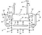
- the switch or switching deviceincludes a bypass circuit portion 10 which in the illustrated embodiment comprises a pair of series-coupled quarter wavelength lines 12 , 14 which are coupled between an input 16 and an output 18 of the circuit.
- the two quarter wave lines 12 and 14are coupled in series by a DC blocking capacitor 20 .
- the input 16is coupled in series with an input of the amplifier or LNA 22 which is to be bypassed by the switch or switching circuit or device of the invention.
- the output 18is coupled in series circuit with the output of this amplifier 22 .
- a pair of switching diodes 24 , 26are coupled between the ends of the respective quarter wavelength lines 12 and 14 which are coupled to the capacitor 20 , and a radio frequency (RF) ground.
- Additional switching diodes 30 and 32are coupled in series respectively with the input 16 and output 18 of the amplifier 22 .
- Respective DC blocking capacitors 34 , 36are coupled respectively intermediate the diodes 30 , 32 and the input and output of the amplifier 22 .
- a source of control bias 40 for the switching circuitis coupled by way of suitable current limiting resistors 42 and 44 and additional quarter wavelength lines 46 and 48 to respective junctions of the diodes 30 and 32 with the capacitors 34 and 36 .
- the polarities of the connections of the diodes 24 , 26 , 30 , and 32are such that with the control bias 40 present or operative, all of the diodes 24 , 26 , 30 , and 32 are biased into a conductive condition, that is forward biased. The effect of this will be to deliver the input signal at the input 16 through the amplifier 22 to the output terminal 18 .
- the control bias 40when the control bias 40 is absent, the diodes 24 , 26 , 30 , and 32 will be in a nonconductive condition, such that the signal path will flow from the input 16 through the quarter wavelength lines 12 and 14 to the output 18 .
- the quarter wavelength lines 12 , 14 , and 46 , 48may be formed as microstrips on a suitable dielectric substrate.
- the circuit of FIG. 1presents an operative device, better performance in terms of insertion loss and isolation can be obtained by the circuit in FIG. 2, which adds a number of resonant circuits, as well as using pairs of diodes 124 , 126 , 130 , and 132 in parallel in place of the single diodes 24 , 26 , 30 , and 32 of FIG. 1 .
- the diodesare M-Pulse Microwave P/N diodes of the type MP5X7084 from M-Pulse Microwave, San Jose, Calif., or equivalent devices. With these diode components selected in the circuit of FIG. 2, insertion loss as low as 0.15 dB and isolation as high as 60 dB is obtainable.
- the control bias voltage 40is applied via a quarter wavelength line 148 to diodes 132 at the output side of the amplifier 22 which will be seen to be connected in reverse polarity to that shown in FIG. 1 .
- Input diodes 130 to the amplifier 22are coupled via a quarter wavelength line 146 , to a DC ground. Both of these diode pairs 130 , 132 are provided with a parallel resonant circuit comprising inductors 60 , 62 and DC blocking capacitors 64 , 66 .
- the inductors 60 and 62will resonate with the respective associated diodes 130 , 132 when in the off or nonconductive state; that is, they are resonant with the residual off state capacitance of the respective associated diodes 130 , 132 .
- the remaining inductors shown in FIG. 2are chokes.
- an additional or third quarter wavelength line 70is provided in series between the quarter wavelength lines 112 , 114 which generally function in the same manner as the bypass circuit of FIG. 1, comprising the quarter wavelength lines 12 , 14 .
- DC blocking capacitors 134 , 136 in the embodiment of FIG. 2are coupled directly to the input 116 and output 118 .
- the diodes 24 , 26are replaced by respective pairs of diodes 124 , 124 a and 126 , 126 a , which are coupled with similar DC bias circuits 80 , 82 .
- the capacitors 90 , 92 and 94 , 96 in these resonant circuitsare selected to series resonate with the diodes 124 , 124 a and 126 , 126 a in the on, or conductive state; that is, with the on state residual inductance of these diodes.
- the other capacitors shown in the respective circuits 80 and 82are bypasses.
- the isolation which is importantis that around the feedback path or leakage path provided by the bypass. That is, with the LNA 22 in the circuit, feedback is to be minimized.
- the LNA gainis about 15 dB so the isolation must be considerably greater than 15 dB. Even at 25 to 30 dB isolation there can be amplitude and group delay “ripples” in the passband. Therefore, the goal is at least 50 dB isolation in the “normal” mode, i.e. with the LNA 22 in the path.
- Diodes 24 , 26 in FIG. 1approximate a short when the LNA 22 is in the path. This cuts off the feedback through the loop. However, the quarter wave lines make this RF “short” look like an RF open circuit at the input and output ends 16 , 18 .
- the resonating inductances and capacitancesare intended to minimize the diodes' ON-state impedances. While the resistive component cannot be changed, the reactance component can be cancelled out by use of the resonating elements. This also enhances the performance of the quarter wave lines and their ability to simulate an open circuit at one end when a diode is in conduction at the other end. It is desired for all of the diodes to have the lowest possible on resistance. As a practical matter, this is on the order of 1 Ohm.
- the biasing schemeis changed from FIG. 1, such that the control bias is applied only at the output side, but the polarities of the diodes are now arranged so that the bypass provides a DC bias path to the anode side of the diodes 130 as well, whose cathodes remain at a ground bias at the quarter wave line 146 .
- the appropriate DC biasis also provided at the anodes/cathodes of the respective diodes 124 , 124 a , 126 , 126 a by the circuit shown in FIG. 2 .
- the quarter wave lines 146 and 148are such that the DC bias can be applied without affecting the RF performance; that is, these look like open circuits to the RF or microwave signal.
- the inductances characterized as chokesare essentially AC blocks and DC shorts. Conversely, the capacitors characterized as bypasses form AC shorts and DC blocks.
- the circuit of FIG. 1will operate acceptably at relatively low frequencies, for example, on the order of 100 MHz, although the quarter wave line lengths may be inconvenient. However, in order to get the noted performance of 0.15 dB insertion loss and 60 dB isolation, when transmitting or receiving at gigahertz frequencies, the somewhat more complex circuit of FIG. 2 is utilized. It will be noted that the use of solid state components and circuitry in place of relays provides additional advantages in that the DC power requirements of the solid state devices are quite low as compared to relatively high power requirements of relays, and also there are no mechanical switching transients with the use of solid state devices, as in the embodiments of the invention shown herein. Moreover, the present cost of the solid state circuit of FIG. 2 is on the order of ten to fifteen percent of circuits using microwave relays as the bypass switching devices.
Landscapes
- Engineering & Computer Science (AREA)
- Power Engineering (AREA)
- Amplifiers (AREA)
Abstract
Description
Claims (49)
Priority Applications (2)
| Application Number | Priority Date | Filing Date | Title |
|---|---|---|---|
| US10/120,750US6700439B2 (en) | 2002-04-11 | 2002-04-11 | Zero-bias bypass switch |
| US10/403,779US6812786B2 (en) | 2002-04-11 | 2003-03-31 | Zero-bias bypass switching circuit using mismatched 90 degrees hybrid |
Applications Claiming Priority (1)
| Application Number | Priority Date | Filing Date | Title |
|---|---|---|---|
| US10/120,750US6700439B2 (en) | 2002-04-11 | 2002-04-11 | Zero-bias bypass switch |
Related Child Applications (1)
| Application Number | Title | Priority Date | Filing Date |
|---|---|---|---|
| US10/403,779Continuation-In-PartUS6812786B2 (en) | 2002-04-11 | 2003-03-31 | Zero-bias bypass switching circuit using mismatched 90 degrees hybrid |
Publications (2)
| Publication Number | Publication Date |
|---|---|
| US20030193368A1 US20030193368A1 (en) | 2003-10-16 |
| US6700439B2true US6700439B2 (en) | 2004-03-02 |
Family
ID=28790158
Family Applications (1)
| Application Number | Title | Priority Date | Filing Date |
|---|---|---|---|
| US10/120,750Expired - LifetimeUS6700439B2 (en) | 2002-04-11 | 2002-04-11 | Zero-bias bypass switch |
Country Status (1)
| Country | Link |
|---|---|
| US (1) | US6700439B2 (en) |
Cited By (14)
| Publication number | Priority date | Publication date | Assignee | Title |
|---|---|---|---|---|
| US20040130391A1 (en)* | 2003-01-03 | 2004-07-08 | Wavics, Inc. | High efficiency power amplifier with multiple power modes |
| US20050099227A1 (en)* | 2003-01-03 | 2005-05-12 | Wavics Inc. | High Efficiency Power Amplifier |
| US20060055447A1 (en)* | 2004-09-14 | 2006-03-16 | Wavics Inc. | Temperature-Compensated Circuit for Power Amplifier Using Diode Voltage Control |
| US20060077001A1 (en)* | 2004-10-11 | 2006-04-13 | Wavics Inc. | Temperature-Compensated Bias Circuit for Power Amplifier |
| US20060164163A1 (en)* | 2005-01-24 | 2006-07-27 | Triquint Semiconductor, Inc. | Amplifiers with high efficiency in multiple power modes |
| US20070018720A1 (en)* | 2005-07-21 | 2007-01-25 | Triquint Semiconductor, Inc. | High efficiency amplifier circuits having bypass paths |
| US20080007327A1 (en)* | 2003-01-03 | 2008-01-10 | Wavics Inc., Delaware Corporation | Multiple power mode amplifier with bias modulation option and without bypass switches |
| US20080164940A1 (en)* | 2007-01-09 | 2008-07-10 | Moon-Suk Jeon | Miltiple output power mode amplifier |
| US20080265988A1 (en)* | 2007-04-24 | 2008-10-30 | Jung Sang Hwa | Multiple output power mode amplifier |
| US7982543B1 (en) | 2009-03-30 | 2011-07-19 | Triquint Semiconductor, Inc. | Switchable power amplifier |
| US8207798B1 (en) | 2009-09-09 | 2012-06-26 | Triquint Semiconductor, Inc. | Matching network with switchable capacitor bank |
| US9337775B1 (en) | 2014-12-05 | 2016-05-10 | Infineon Technologies Ag | System and method for a low noise amplifier module |
| US9479126B2 (en) | 2014-08-19 | 2016-10-25 | Infineon Technologies Ag | System and method for a low noise amplifier |
| US9985586B2 (en) | 2015-05-29 | 2018-05-29 | Samsung Electro-Mechanics Co., Ltd. | Front end circuit |
Families Citing this family (2)
| Publication number | Priority date | Publication date | Assignee | Title |
|---|---|---|---|---|
| US9048940B2 (en)* | 2012-08-31 | 2015-06-02 | Clear Rf, Llc | Passive bypass for network extending |
| KR102185059B1 (en)* | 2018-08-17 | 2020-12-01 | 삼성전기주식회사 | Amplifying device with improved isolation characteristics |
Citations (65)
| Publication number | Priority date | Publication date | Assignee | Title |
|---|---|---|---|---|
| US4291277A (en) | 1979-05-16 | 1981-09-22 | Harris Corporation | Adaptive predistortion technique for linearizing a power amplifier for digital data systems |
| US4967164A (en) | 1988-09-30 | 1990-10-30 | U.S. Philips Corporation | Adaptive predistortion circuit |
| US5105445A (en) | 1989-10-06 | 1992-04-14 | U.S. Philips Corporation | Predistortion arrangement for a digital transmission system |
| US5105446A (en) | 1989-10-18 | 1992-04-14 | Alcatel Transmission Par Faisceaux Hertziens | Digital method of correcting non-linearity in a transmission chain, and apparatus implementing the method |
| US5107520A (en) | 1989-01-24 | 1992-04-21 | U.S. Philips Corporation | Adaptive predistortion circuit for a digital transmission system |
| US5113414A (en) | 1989-10-06 | 1992-05-12 | U.S. Philips Corporation | Predistortion arrangement for a digital transmission system |
| US5148448A (en) | 1989-03-14 | 1992-09-15 | U.S. Philips Corporation | Adaptive predistortion circuit with memory |
| US5155448A (en) | 1989-11-16 | 1992-10-13 | Motorola, Inc. | Feed-forward amplifier having increased compression point |
| US5157346A (en) | 1989-11-16 | 1992-10-20 | Motorola, Inc. | Rf wideband high power amplifier |
| US5323119A (en) | 1989-11-16 | 1994-06-21 | Motorola, Inc. | Amplifier having feed forward cancellation |
| US5386198A (en) | 1993-01-28 | 1995-01-31 | Telefonaktiebolaget L M Ericsson | Linear amplifier control |
| US5444418A (en) | 1994-07-29 | 1995-08-22 | Motorola, Inc. | Method and apparatus for feedforward power amplifying |
| US5491454A (en) | 1994-10-31 | 1996-02-13 | Motorola, Inc. | Method and apparatus for reducing distortion in an output signal of an amplifier |
| US5508657A (en) | 1995-01-30 | 1996-04-16 | Aml Communications, Inc. | Feed forward cancellation amplifier utilizing dynamic vector control |
| US5524286A (en) | 1993-12-14 | 1996-06-04 | Alcatel Italia S.P.A. | Baseband predistortion system for the adaptive linearization of power amplifiers |
| US5528196A (en) | 1995-01-06 | 1996-06-18 | Spectrian, Inc. | Linear RF amplifier having reduced intermodulation distortion |
| US5570063A (en) | 1995-05-18 | 1996-10-29 | Spectrian, Inc. | RF power amplifier with signal predistortion for improved linearity |
| US5589797A (en) | 1995-09-26 | 1996-12-31 | Lucent Technologies Inc. | Low distortion amplifier |
| US5598436A (en) | 1993-06-29 | 1997-01-28 | U.S. Philips Corporation | Digital transmission system with predistortion |
| US5619168A (en) | 1995-08-07 | 1997-04-08 | Lucent Technologies Inc. | Distortion creation and reduction circuit |
| US5621354A (en) | 1995-10-17 | 1997-04-15 | Motorola, Inc. | Apparatus and method for performing error corrected amplification in a radio frequency system |
| US5644268A (en) | 1995-01-06 | 1997-07-01 | Spectrian, Inc. | Feed forward RF amplifier for combined signal and error amplification |
| US5732333A (en) | 1996-02-14 | 1998-03-24 | Glenayre Electronics, Inc. | Linear transmitter using predistortion |
| US5742201A (en) | 1996-01-30 | 1998-04-21 | Spectrian | Polar envelope correction mechanism for enhancing linearity of RF/microwave power amplifier |
| US5745006A (en) | 1996-11-12 | 1998-04-28 | Motorola, Inc. | Method of compensating for distortion in an amplifier |
| US5748678A (en) | 1995-07-13 | 1998-05-05 | Motorola, Inc. | Radio communications apparatus |
| US5757231A (en) | 1995-11-16 | 1998-05-26 | Fujitsu Limited | Feed-forward amplifying device and base station with feed-forward amplifying device |
| US5760646A (en) | 1996-03-29 | 1998-06-02 | Spectrian | Feed-forward correction loop with adaptive predistortion injection for linearization of RF power amplifier |
| US5789927A (en) | 1996-06-28 | 1998-08-04 | Spectrian | Baseband measurement of RF power amplifier distortion |
| US5796304A (en) | 1996-04-24 | 1998-08-18 | Powerwave Technologies, Inc. | Broadband amplifier with quadrature pilot signal |
| US5808512A (en) | 1997-01-31 | 1998-09-15 | Ophir Rf, Inc. | Feed forward amplifiers and methods |
| US5867064A (en) | 1996-08-19 | 1999-02-02 | Motorola, Inc. | Method and apparatus for improving intermodulation in a feed-forward amplifier |
| US5872814A (en) | 1997-02-24 | 1999-02-16 | At&T Wireless Services Inc. | Method for linearization of RF transmission electronics using baseband pre-distortion in T/R compensation pilot signals |
| US5877653A (en) | 1995-11-16 | 1999-03-02 | Samsung Electronics Co., Ltd. | Linear power amplifier and method for removing intermodulation distortion with predistortion system and feed forward system |
| US5892397A (en) | 1996-03-29 | 1999-04-06 | Spectrian | Adaptive compensation of RF amplifier distortion by injecting predistortion signal derived from respectively different functions of input signal amplitude |
| US5898338A (en) | 1996-09-20 | 1999-04-27 | Spectrian | Adaptive digital predistortion linearization and feed-forward correction of RF power amplifier |
| US5898906A (en) | 1996-10-29 | 1999-04-27 | Gec Plessey Semiconductors, Inc. | System and method for implementing a cellular radio transmitter device |
| US5903611A (en) | 1996-03-22 | 1999-05-11 | Matra Communication | Method of correcting nonlinearities of an amplifier, and radio transmitter employing a method of this type |
| US5905760A (en) | 1996-03-22 | 1999-05-18 | Matra Communication | Method of correcting nonlinearities of an amplifier, and radio transmitter employing a method of this type |
| US5917375A (en) | 1995-09-08 | 1999-06-29 | Lucent Technologies Inc. | Low distortion amplifier circuit with improved output power |
| US5929703A (en) | 1996-08-07 | 1999-07-27 | Alcatel Telspace | Method and device for modeling AM-AM and AM-PM characteristics of an amplifier, and corresponding predistortion method |
| US5929704A (en) | 1998-02-20 | 1999-07-27 | Spectrian | Control of RF error extraction using auto-calibrating RF correlator |
| US5937011A (en) | 1996-03-26 | 1999-08-10 | Airnet Communications Corp. | Multi-carrier high power amplifier using digital pre-distortion |
| US5963090A (en) | 1996-11-13 | 1999-10-05 | Nec Corporation | Automatic predistortion adjusting circuit having stable non-linear characteristics regardless of input signal frequency |
| US5986499A (en) | 1998-12-21 | 1999-11-16 | Lucent Technologies Inc. | Pilot signal detection system using band reject filter |
| US6028477A (en) | 1998-04-08 | 2000-02-22 | Powerwave Technologies, Inc. | Adaptive biasing in a power amplifier |
| US6046635A (en) | 1998-04-08 | 2000-04-04 | Powerwave Technologies, Inc. | Dynamic predistortion compensation for a power amplifier |
| US6049707A (en) | 1997-09-02 | 2000-04-11 | Motorola, Inc. | Broadband multicarrier amplifier system and method using envelope elimination and restoration |
| US6052023A (en) | 1998-08-31 | 2000-04-18 | Lucent Technologies Inc. | Calibration system for feed forward distortion reduction system |
| US6057733A (en) | 1997-12-18 | 2000-05-02 | Lucent Technologies, Inc. | Feedforward multicarrier linear RF power amplifier |
| US6060949A (en)* | 1998-09-22 | 2000-05-09 | Qualcomm Incorporated | High efficiency switched gain power amplifier |
| US6066984A (en) | 1998-03-16 | 2000-05-23 | Hitachi Denshi Kabushiki Kaisha | Amplifier and amplifying method for amplifying a plurality of signals having different bands simultaneously |
| US6069526A (en)* | 1998-08-04 | 2000-05-30 | Qualcomm Incorporated | Partial or complete amplifier bypass |
| US6075411A (en) | 1997-12-22 | 2000-06-13 | Telefonaktiebolaget Lm Ericsson | Method and apparatus for wideband predistortion linearization |
| US6078216A (en) | 1998-03-31 | 2000-06-20 | Spectrian Corporation | Aliased wide band performance monitor for adjusting predistortion and vector modulator control parameters of RF amplifier |
| US6081160A (en) | 1998-05-20 | 2000-06-27 | Powerwave Technologies, Inc. | Method and apparatus for increasing the bandwidth, and reducing the size, of the DC feed network for wideband RF amplifiers using selective placement of high dielectric constant material |
| US6081156A (en) | 1997-12-26 | 2000-06-27 | Samsung Electronics Co., Ltd. | Method and apparatus for amplifying feedforward linear power using pilot tone hopping |
| US6104241A (en) | 1998-11-18 | 2000-08-15 | Spectrian | High efficiency feed-forward RF power amplifier with predistoration enchancement |
| US6108385A (en) | 1996-07-08 | 2000-08-22 | Silicon Wireless Limited | Method and apparatus for reducing intermodulation distortion in digital wideband transmission systems |
| US6118339A (en) | 1998-10-19 | 2000-09-12 | Powerwave Technologies, Inc. | Amplification system using baseband mixer |
| US6125266A (en) | 1997-12-31 | 2000-09-26 | Nokia Mobile Phones Limited | Dual band architectures for mobile stations having transmitter linearization feedback |
| US6127889A (en) | 1998-11-18 | 2000-10-03 | Lucent Technologies Inc. | Nested feed forward distortion reduction system |
| US6140874A (en) | 1998-10-19 | 2000-10-31 | Powerwave Technologies, Inc. | Amplification system having mask detection and bias compensation |
| US6144255A (en) | 1998-10-19 | 2000-11-07 | Powerwave Technologies, Inc. | Feedforward amplification system having mask detection compensation |
| US6362685B1 (en)* | 2000-07-20 | 2002-03-26 | Rockwell Collins, Inc. | Power amplifier with multilevel power modes |
- 2002
- 2002-04-11USUS10/120,750patent/US6700439B2/ennot_activeExpired - Lifetime
Patent Citations (67)
| Publication number | Priority date | Publication date | Assignee | Title |
|---|---|---|---|---|
| US4291277A (en) | 1979-05-16 | 1981-09-22 | Harris Corporation | Adaptive predistortion technique for linearizing a power amplifier for digital data systems |
| US4967164A (en) | 1988-09-30 | 1990-10-30 | U.S. Philips Corporation | Adaptive predistortion circuit |
| US5107520A (en) | 1989-01-24 | 1992-04-21 | U.S. Philips Corporation | Adaptive predistortion circuit for a digital transmission system |
| US5148448A (en) | 1989-03-14 | 1992-09-15 | U.S. Philips Corporation | Adaptive predistortion circuit with memory |
| US5105445A (en) | 1989-10-06 | 1992-04-14 | U.S. Philips Corporation | Predistortion arrangement for a digital transmission system |
| US5113414A (en) | 1989-10-06 | 1992-05-12 | U.S. Philips Corporation | Predistortion arrangement for a digital transmission system |
| US5105446A (en) | 1989-10-18 | 1992-04-14 | Alcatel Transmission Par Faisceaux Hertziens | Digital method of correcting non-linearity in a transmission chain, and apparatus implementing the method |
| US5155448A (en) | 1989-11-16 | 1992-10-13 | Motorola, Inc. | Feed-forward amplifier having increased compression point |
| US5157346A (en) | 1989-11-16 | 1992-10-20 | Motorola, Inc. | Rf wideband high power amplifier |
| US5323119A (en) | 1989-11-16 | 1994-06-21 | Motorola, Inc. | Amplifier having feed forward cancellation |
| US5386198A (en) | 1993-01-28 | 1995-01-31 | Telefonaktiebolaget L M Ericsson | Linear amplifier control |
| US5598436A (en) | 1993-06-29 | 1997-01-28 | U.S. Philips Corporation | Digital transmission system with predistortion |
| US5524286A (en) | 1993-12-14 | 1996-06-04 | Alcatel Italia S.P.A. | Baseband predistortion system for the adaptive linearization of power amplifiers |
| US5444418A (en) | 1994-07-29 | 1995-08-22 | Motorola, Inc. | Method and apparatus for feedforward power amplifying |
| US5491454A (en) | 1994-10-31 | 1996-02-13 | Motorola, Inc. | Method and apparatus for reducing distortion in an output signal of an amplifier |
| US5528196A (en) | 1995-01-06 | 1996-06-18 | Spectrian, Inc. | Linear RF amplifier having reduced intermodulation distortion |
| US5644268A (en) | 1995-01-06 | 1997-07-01 | Spectrian, Inc. | Feed forward RF amplifier for combined signal and error amplification |
| US5508657A (en) | 1995-01-30 | 1996-04-16 | Aml Communications, Inc. | Feed forward cancellation amplifier utilizing dynamic vector control |
| US5570063A (en) | 1995-05-18 | 1996-10-29 | Spectrian, Inc. | RF power amplifier with signal predistortion for improved linearity |
| US5748678A (en) | 1995-07-13 | 1998-05-05 | Motorola, Inc. | Radio communications apparatus |
| US5619168A (en) | 1995-08-07 | 1997-04-08 | Lucent Technologies Inc. | Distortion creation and reduction circuit |
| US5917375A (en) | 1995-09-08 | 1999-06-29 | Lucent Technologies Inc. | Low distortion amplifier circuit with improved output power |
| US5589797A (en) | 1995-09-26 | 1996-12-31 | Lucent Technologies Inc. | Low distortion amplifier |
| US5621354A (en) | 1995-10-17 | 1997-04-15 | Motorola, Inc. | Apparatus and method for performing error corrected amplification in a radio frequency system |
| US5757231A (en) | 1995-11-16 | 1998-05-26 | Fujitsu Limited | Feed-forward amplifying device and base station with feed-forward amplifying device |
| US5877653A (en) | 1995-11-16 | 1999-03-02 | Samsung Electronics Co., Ltd. | Linear power amplifier and method for removing intermodulation distortion with predistortion system and feed forward system |
| US5742201A (en) | 1996-01-30 | 1998-04-21 | Spectrian | Polar envelope correction mechanism for enhancing linearity of RF/microwave power amplifier |
| US5732333A (en) | 1996-02-14 | 1998-03-24 | Glenayre Electronics, Inc. | Linear transmitter using predistortion |
| US5903611A (en) | 1996-03-22 | 1999-05-11 | Matra Communication | Method of correcting nonlinearities of an amplifier, and radio transmitter employing a method of this type |
| US5905760A (en) | 1996-03-22 | 1999-05-18 | Matra Communication | Method of correcting nonlinearities of an amplifier, and radio transmitter employing a method of this type |
| US5937011A (en) | 1996-03-26 | 1999-08-10 | Airnet Communications Corp. | Multi-carrier high power amplifier using digital pre-distortion |
| US6029285A (en) | 1996-03-29 | 2000-02-29 | Spectrian | Adaptive compensation of RF amplifier distortion by injecting predistortion signal derived from respectively different functions of input signal amplitude |
| US5892397A (en) | 1996-03-29 | 1999-04-06 | Spectrian | Adaptive compensation of RF amplifier distortion by injecting predistortion signal derived from respectively different functions of input signal amplitude |
| US5760646A (en) | 1996-03-29 | 1998-06-02 | Spectrian | Feed-forward correction loop with adaptive predistortion injection for linearization of RF power amplifier |
| US5796304A (en) | 1996-04-24 | 1998-08-18 | Powerwave Technologies, Inc. | Broadband amplifier with quadrature pilot signal |
| US5789927A (en) | 1996-06-28 | 1998-08-04 | Spectrian | Baseband measurement of RF power amplifier distortion |
| US6108385A (en) | 1996-07-08 | 2000-08-22 | Silicon Wireless Limited | Method and apparatus for reducing intermodulation distortion in digital wideband transmission systems |
| US5929703A (en) | 1996-08-07 | 1999-07-27 | Alcatel Telspace | Method and device for modeling AM-AM and AM-PM characteristics of an amplifier, and corresponding predistortion method |
| US5867064A (en) | 1996-08-19 | 1999-02-02 | Motorola, Inc. | Method and apparatus for improving intermodulation in a feed-forward amplifier |
| US5898338A (en) | 1996-09-20 | 1999-04-27 | Spectrian | Adaptive digital predistortion linearization and feed-forward correction of RF power amplifier |
| US5949283A (en) | 1996-09-20 | 1999-09-07 | Spectrian | Adaptive digital predistortion linearization and feed-forward correction of RF power amplifier |
| US5898906A (en) | 1996-10-29 | 1999-04-27 | Gec Plessey Semiconductors, Inc. | System and method for implementing a cellular radio transmitter device |
| US5745006A (en) | 1996-11-12 | 1998-04-28 | Motorola, Inc. | Method of compensating for distortion in an amplifier |
| US5963090A (en) | 1996-11-13 | 1999-10-05 | Nec Corporation | Automatic predistortion adjusting circuit having stable non-linear characteristics regardless of input signal frequency |
| US5808512A (en) | 1997-01-31 | 1998-09-15 | Ophir Rf, Inc. | Feed forward amplifiers and methods |
| US5872814A (en) | 1997-02-24 | 1999-02-16 | At&T Wireless Services Inc. | Method for linearization of RF transmission electronics using baseband pre-distortion in T/R compensation pilot signals |
| US6049707A (en) | 1997-09-02 | 2000-04-11 | Motorola, Inc. | Broadband multicarrier amplifier system and method using envelope elimination and restoration |
| US6057733A (en) | 1997-12-18 | 2000-05-02 | Lucent Technologies, Inc. | Feedforward multicarrier linear RF power amplifier |
| US6075411A (en) | 1997-12-22 | 2000-06-13 | Telefonaktiebolaget Lm Ericsson | Method and apparatus for wideband predistortion linearization |
| US6081156A (en) | 1997-12-26 | 2000-06-27 | Samsung Electronics Co., Ltd. | Method and apparatus for amplifying feedforward linear power using pilot tone hopping |
| US6125266A (en) | 1997-12-31 | 2000-09-26 | Nokia Mobile Phones Limited | Dual band architectures for mobile stations having transmitter linearization feedback |
| US5929704A (en) | 1998-02-20 | 1999-07-27 | Spectrian | Control of RF error extraction using auto-calibrating RF correlator |
| US6066984A (en) | 1998-03-16 | 2000-05-23 | Hitachi Denshi Kabushiki Kaisha | Amplifier and amplifying method for amplifying a plurality of signals having different bands simultaneously |
| US6078216A (en) | 1998-03-31 | 2000-06-20 | Spectrian Corporation | Aliased wide band performance monitor for adjusting predistortion and vector modulator control parameters of RF amplifier |
| US6046635A (en) | 1998-04-08 | 2000-04-04 | Powerwave Technologies, Inc. | Dynamic predistortion compensation for a power amplifier |
| US6028477A (en) | 1998-04-08 | 2000-02-22 | Powerwave Technologies, Inc. | Adaptive biasing in a power amplifier |
| US6081160A (en) | 1998-05-20 | 2000-06-27 | Powerwave Technologies, Inc. | Method and apparatus for increasing the bandwidth, and reducing the size, of the DC feed network for wideband RF amplifiers using selective placement of high dielectric constant material |
| US6069526A (en)* | 1998-08-04 | 2000-05-30 | Qualcomm Incorporated | Partial or complete amplifier bypass |
| US6052023A (en) | 1998-08-31 | 2000-04-18 | Lucent Technologies Inc. | Calibration system for feed forward distortion reduction system |
| US6060949A (en)* | 1998-09-22 | 2000-05-09 | Qualcomm Incorporated | High efficiency switched gain power amplifier |
| US6140874A (en) | 1998-10-19 | 2000-10-31 | Powerwave Technologies, Inc. | Amplification system having mask detection and bias compensation |
| US6118339A (en) | 1998-10-19 | 2000-09-12 | Powerwave Technologies, Inc. | Amplification system using baseband mixer |
| US6144255A (en) | 1998-10-19 | 2000-11-07 | Powerwave Technologies, Inc. | Feedforward amplification system having mask detection compensation |
| US6104241A (en) | 1998-11-18 | 2000-08-15 | Spectrian | High efficiency feed-forward RF power amplifier with predistoration enchancement |
| US6127889A (en) | 1998-11-18 | 2000-10-03 | Lucent Technologies Inc. | Nested feed forward distortion reduction system |
| US5986499A (en) | 1998-12-21 | 1999-11-16 | Lucent Technologies Inc. | Pilot signal detection system using band reject filter |
| US6362685B1 (en)* | 2000-07-20 | 2002-03-26 | Rockwell Collins, Inc. | Power amplifier with multilevel power modes |
Cited By (38)
| Publication number | Priority date | Publication date | Assignee | Title |
|---|---|---|---|---|
| US20080007329A1 (en)* | 2003-01-03 | 2008-01-10 | Wavics Inc., Delaware Corporation | Multiple power mode amplifier with bias modulation option and without bypass switches |
| US20080007327A1 (en)* | 2003-01-03 | 2008-01-10 | Wavics Inc., Delaware Corporation | Multiple power mode amplifier with bias modulation option and without bypass switches |
| US20050099227A1 (en)* | 2003-01-03 | 2005-05-12 | Wavics Inc. | High Efficiency Power Amplifier |
| US6900692B2 (en)* | 2003-01-03 | 2005-05-31 | Wavics, Inc. | High efficiency power amplifier with multiple power modes |
| US20050122165A1 (en)* | 2003-01-03 | 2005-06-09 | Wavics Inc. | High efficiency power amplifier with multiple power modes |
| US6972618B2 (en)* | 2003-01-03 | 2005-12-06 | Wavics, Inc. | High efficiency power amplifier with multiple power modes |
| US7049886B2 (en)* | 2003-01-03 | 2006-05-23 | Junghyun Kim | High efficiency power amplifier with multiple power modes |
| US7023270B2 (en)* | 2003-01-03 | 2006-04-04 | Junghyun Kim | High efficiency power amplifier |
| US20080012635A1 (en)* | 2003-01-03 | 2008-01-17 | Wavies, Inc. | Multiple power mode amplifier with bias modulation option and without bypass switches |
| US7420412B2 (en)* | 2003-01-03 | 2008-09-02 | Junghyun Kim | Multiple power mode amplifier with bias modulation option and without bypass switches |
| US20040130391A1 (en)* | 2003-01-03 | 2004-07-08 | Wavics, Inc. | High efficiency power amplifier with multiple power modes |
| US20060261887A1 (en)* | 2003-01-03 | 2006-11-23 | Avago Technologies | High efficiency power amplifier |
| US7394313B2 (en)* | 2003-01-03 | 2008-07-01 | Avago Technologies General Ip (Singapore) Pte. Ltd | Multiple power mode amplifier with bias modulation option and without bypass switches |
| US20050068101A1 (en)* | 2003-01-03 | 2005-03-31 | Wavics, Inc. | High efficiency power amplification apparatus with multiple power modes |
| US7215192B2 (en)* | 2003-01-03 | 2007-05-08 | Junghyun Kim | High efficiency power amplifier |
| US20080007328A1 (en)* | 2003-01-03 | 2008-01-10 | Wavics, Inc. | Multiple power mode amplifier with bias modulation option and without bypass switches |
| US7388427B2 (en)* | 2003-01-03 | 2008-06-17 | Avago Technologies General Ip (Singapore) Pte. Ltd. | Multiple power mode amplifier with bias modulation option and without bypass switches |
| US7310015B2 (en) | 2004-09-14 | 2007-12-18 | Avago Technologies Wireless Ip Pte. Ltd. | Temperature-compensated circuit for power amplifier using diode voltage control |
| US20060055447A1 (en)* | 2004-09-14 | 2006-03-16 | Wavics Inc. | Temperature-Compensated Circuit for Power Amplifier Using Diode Voltage Control |
| US7193452B2 (en) | 2004-10-11 | 2007-03-20 | Moon-Suk Jeon | Temperature-compensated bias circuit for power amplifier |
| US20060077001A1 (en)* | 2004-10-11 | 2006-04-13 | Wavics Inc. | Temperature-Compensated Bias Circuit for Power Amplifier |
| US20060164163A1 (en)* | 2005-01-24 | 2006-07-27 | Triquint Semiconductor, Inc. | Amplifiers with high efficiency in multiple power modes |
| US7382186B2 (en) | 2005-01-24 | 2008-06-03 | Triquint Semiconductor, Inc. | Amplifiers with high efficiency in multiple power modes |
| US20070018720A1 (en)* | 2005-07-21 | 2007-01-25 | Triquint Semiconductor, Inc. | High efficiency amplifier circuits having bypass paths |
| US7385445B2 (en)* | 2005-07-21 | 2008-06-10 | Triquint Semiconductor, Inc. | High efficiency amplifier circuits having bypass paths |
| US20090309656A1 (en)* | 2007-01-09 | 2009-12-17 | Avago Technologies Wireless Ip (Singapore) Pte. Ltd. | Multiple output power mode amplifier |
| US20080164940A1 (en)* | 2007-01-09 | 2008-07-10 | Moon-Suk Jeon | Miltiple output power mode amplifier |
| US7714647B2 (en) | 2007-01-09 | 2010-05-11 | Avago Technologies Wireless Ip (Singapore) Pte. Ltd. | Multiple output power mode amplifier |
| US7616054B2 (en) | 2007-01-09 | 2009-11-10 | Avago Technologies Wireless Ip (Singapore) Pte. Ltd. | Multiple output power mode amplifier |
| US20080265988A1 (en)* | 2007-04-24 | 2008-10-30 | Jung Sang Hwa | Multiple output power mode amplifier |
| US7554392B2 (en) | 2007-04-24 | 2009-06-30 | Avago Technologies Wireless Ip (Singapore) Pte. Ltd. | Multiple output power mode amplifier |
| US7982543B1 (en) | 2009-03-30 | 2011-07-19 | Triquint Semiconductor, Inc. | Switchable power amplifier |
| US8207798B1 (en) | 2009-09-09 | 2012-06-26 | Triquint Semiconductor, Inc. | Matching network with switchable capacitor bank |
| US9479126B2 (en) | 2014-08-19 | 2016-10-25 | Infineon Technologies Ag | System and method for a low noise amplifier |
| US9337775B1 (en) | 2014-12-05 | 2016-05-10 | Infineon Technologies Ag | System and method for a low noise amplifier module |
| US9742364B2 (en) | 2014-12-05 | 2017-08-22 | Infineon Technologies Ag | System and method for a low noise amplifier module |
| US9985586B2 (en) | 2015-05-29 | 2018-05-29 | Samsung Electro-Mechanics Co., Ltd. | Front end circuit |
| US10305434B2 (en)* | 2015-05-29 | 2019-05-28 | Samsung Electro-Mechanics Co., Ltd. | Front end circuit |
Also Published As
| Publication number | Publication date |
|---|---|
| US20030193368A1 (en) | 2003-10-16 |
Similar Documents
| Publication | Publication Date | Title |
|---|---|---|
| US6700439B2 (en) | Zero-bias bypass switch | |
| US5594394A (en) | Antenna diversity switching device with switching circuits between the receiver terminal and each antenna | |
| US6812786B2 (en) | Zero-bias bypass switching circuit using mismatched 90 degrees hybrid | |
| US5584053A (en) | Commonly coupled high frequency transmitting/receiving switching module | |
| US7239852B2 (en) | Asymmetric, optimized common-source bi-directional amplifier | |
| US20070232241A1 (en) | RF transceiver switching system | |
| US5625894A (en) | Switch filter having selectively interconnected filter stages and ports | |
| US7075386B2 (en) | Antenna switching circuit | |
| US6552626B2 (en) | High power pin diode switch | |
| US8149049B2 (en) | Low noise receiving apparatus | |
| US6021318A (en) | Transceiver switchover arrangement | |
| JP5259182B2 (en) | Quadrature offset power amplifier | |
| WO2005101670A2 (en) | Apparatus, methods and articles of manufacture for output impedance matching using multi-band signal processing | |
| US11323147B1 (en) | Reducing insertion loss in a switch for a communication device | |
| EP1492245B1 (en) | Transmitting-receiving switch | |
| KR20210126968A (en) | Radio frequency splitter and front-end module | |
| JP2006333023A (en) | High frequency power transmission circuit | |
| KR20020070137A (en) | High-freguency switch circuit suppressing the distortion of high freguency signal | |
| US7548732B2 (en) | Power amplifier arrangement having two or more antenna coupling respective amplifiers to a supply potential | |
| US20250047250A1 (en) | Radio frequency circuit and communication device | |
| US6801757B2 (en) | Circuit configuration for matching an amplifier to a radio-frequency line, and use of the circuit configuration | |
| JP3408712B2 (en) | Front end circuit | |
| KR19990049179A (en) | RF Switch with Phase Correction Circuit | |
| JP2003110457A (en) | Switch circuit and method of using the same | |
| HK1034002B (en) | Monolithic high frequency antenna switch |
Legal Events
| Date | Code | Title | Description |
|---|---|---|---|
| AS | Assignment | Owner name:ANDREW CORPORATION, ILLINOIS Free format text:ASSIGNMENT OF ASSIGNORS INTEREST;ASSIGNOR:JACKSON, DONALD G.;REEL/FRAME:012794/0080 Effective date:20020322 | |
| STCF | Information on status: patent grant | Free format text:PATENTED CASE | |
| FPAY | Fee payment | Year of fee payment:4 | |
| AS | Assignment | Owner name:BANK OF AMERICA, N.A., AS ADMINISTRATIVE AGENT, CA Free format text:SECURITY AGREEMENT;ASSIGNORS:COMMSCOPE, INC. OF NORTH CAROLINA;ALLEN TELECOM, LLC;ANDREW CORPORATION;REEL/FRAME:020362/0241 Effective date:20071227 Owner name:BANK OF AMERICA, N.A., AS ADMINISTRATIVE AGENT,CAL Free format text:SECURITY AGREEMENT;ASSIGNORS:COMMSCOPE, INC. OF NORTH CAROLINA;ALLEN TELECOM, LLC;ANDREW CORPORATION;REEL/FRAME:020362/0241 Effective date:20071227 | |
| AS | Assignment | Owner name:ANDREW LLC, NORTH CAROLINA Free format text:CHANGE OF NAME;ASSIGNOR:ANDREW CORPORATION;REEL/FRAME:021805/0044 Effective date:20080827 | |
| AS | Assignment | Owner name:ALLEN TELECOM LLC, NORTH CAROLINA Free format text:PATENT RELEASE;ASSIGNOR:BANK OF AMERICA, N.A., AS ADMINISTRATIVE AGENT;REEL/FRAME:026039/0005 Effective date:20110114 Owner name:ANDREW LLC (F/K/A ANDREW CORPORATION), NORTH CAROL Free format text:PATENT RELEASE;ASSIGNOR:BANK OF AMERICA, N.A., AS ADMINISTRATIVE AGENT;REEL/FRAME:026039/0005 Effective date:20110114 Owner name:COMMSCOPE, INC. OF NORTH CAROLINA, NORTH CAROLINA Free format text:PATENT RELEASE;ASSIGNOR:BANK OF AMERICA, N.A., AS ADMINISTRATIVE AGENT;REEL/FRAME:026039/0005 Effective date:20110114 | |
| AS | Assignment | Owner name:JPMORGAN CHASE BANK, N.A., AS COLLATERAL AGENT, NE Free format text:SECURITY AGREEMENT;ASSIGNORS:ALLEN TELECOM LLC, A DELAWARE LLC;ANDREW LLC, A DELAWARE LLC;COMMSCOPE, INC. OF NORTH CAROLINA, A NORTH CAROLINA CORPORATION;REEL/FRAME:026276/0363 Effective date:20110114 | |
| AS | Assignment | Owner name:JPMORGAN CHASE BANK, N.A., AS COLLATERAL AGENT, NE Free format text:SECURITY AGREEMENT;ASSIGNORS:ALLEN TELECOM LLC, A DELAWARE LLC;ANDREW LLC, A DELAWARE LLC;COMMSCOPE, INC OF NORTH CAROLINA, A NORTH CAROLINA CORPORATION;REEL/FRAME:026272/0543 Effective date:20110114 | |
| FPAY | Fee payment | Year of fee payment:8 | |
| AS | Assignment | Owner name:COMMSCOPE TECHNOLOGIES LLC, NORTH CAROLINA Free format text:CHANGE OF NAME;ASSIGNOR:ANDREW LLC;REEL/FRAME:035226/0949 Effective date:20150301 | |
| AS | Assignment | Owner name:WILMINGTON TRUST, NATIONAL ASSOCIATION, AS COLLATERAL AGENT, CONNECTICUT Free format text:SECURITY INTEREST;ASSIGNORS:ALLEN TELECOM LLC;COMMSCOPE TECHNOLOGIES LLC;COMMSCOPE, INC. OF NORTH CAROLINA;AND OTHERS;REEL/FRAME:036201/0283 Effective date:20150611 Owner name:WILMINGTON TRUST, NATIONAL ASSOCIATION, AS COLLATE Free format text:SECURITY INTEREST;ASSIGNORS:ALLEN TELECOM LLC;COMMSCOPE TECHNOLOGIES LLC;COMMSCOPE, INC. OF NORTH CAROLINA;AND OTHERS;REEL/FRAME:036201/0283 Effective date:20150611 | |
| REMI | Maintenance fee reminder mailed | ||
| FPAY | Fee payment | Year of fee payment:12 | |
| SULP | Surcharge for late payment | Year of fee payment:11 | |
| AS | Assignment | Owner name:COMMSCOPE TECHNOLOGIES LLC, NORTH CAROLINA Free format text:RELEASE OF SECURITY INTEREST PATENTS (RELEASES RF 036201/0283);ASSIGNOR:WILMINGTON TRUST, NATIONAL ASSOCIATION;REEL/FRAME:042126/0434 Effective date:20170317 Owner name:REDWOOD SYSTEMS, INC., NORTH CAROLINA Free format text:RELEASE OF SECURITY INTEREST PATENTS (RELEASES RF 036201/0283);ASSIGNOR:WILMINGTON TRUST, NATIONAL ASSOCIATION;REEL/FRAME:042126/0434 Effective date:20170317 Owner name:COMMSCOPE, INC. OF NORTH CAROLINA, NORTH CAROLINA Free format text:RELEASE OF SECURITY INTEREST PATENTS (RELEASES RF 036201/0283);ASSIGNOR:WILMINGTON TRUST, NATIONAL ASSOCIATION;REEL/FRAME:042126/0434 Effective date:20170317 Owner name:ALLEN TELECOM LLC, NORTH CAROLINA Free format text:RELEASE OF SECURITY INTEREST PATENTS (RELEASES RF 036201/0283);ASSIGNOR:WILMINGTON TRUST, NATIONAL ASSOCIATION;REEL/FRAME:042126/0434 Effective date:20170317 | |
| AS | Assignment | Owner name:COMMSCOPE TECHNOLOGIES LLC, NORTH CAROLINA Free format text:RELEASE BY SECURED PARTY;ASSIGNOR:JPMORGAN CHASE BANK, N.A.;REEL/FRAME:048840/0001 Effective date:20190404 Owner name:COMMSCOPE, INC. OF NORTH CAROLINA, NORTH CAROLINA Free format text:RELEASE BY SECURED PARTY;ASSIGNOR:JPMORGAN CHASE BANK, N.A.;REEL/FRAME:048840/0001 Effective date:20190404 Owner name:ALLEN TELECOM LLC, ILLINOIS Free format text:RELEASE BY SECURED PARTY;ASSIGNOR:JPMORGAN CHASE BANK, N.A.;REEL/FRAME:048840/0001 Effective date:20190404 Owner name:ANDREW LLC, NORTH CAROLINA Free format text:RELEASE BY SECURED PARTY;ASSIGNOR:JPMORGAN CHASE BANK, N.A.;REEL/FRAME:048840/0001 Effective date:20190404 Owner name:REDWOOD SYSTEMS, INC., NORTH CAROLINA Free format text:RELEASE BY SECURED PARTY;ASSIGNOR:JPMORGAN CHASE BANK, N.A.;REEL/FRAME:048840/0001 Effective date:20190404 Owner name:ALLEN TELECOM LLC, ILLINOIS Free format text:RELEASE BY SECURED PARTY;ASSIGNOR:JPMORGAN CHASE BANK, N.A.;REEL/FRAME:049260/0001 Effective date:20190404 Owner name:ANDREW LLC, NORTH CAROLINA Free format text:RELEASE BY SECURED PARTY;ASSIGNOR:JPMORGAN CHASE BANK, N.A.;REEL/FRAME:049260/0001 Effective date:20190404 Owner name:REDWOOD SYSTEMS, INC., NORTH CAROLINA Free format text:RELEASE BY SECURED PARTY;ASSIGNOR:JPMORGAN CHASE BANK, N.A.;REEL/FRAME:049260/0001 Effective date:20190404 Owner name:COMMSCOPE TECHNOLOGIES LLC, NORTH CAROLINA Free format text:RELEASE BY SECURED PARTY;ASSIGNOR:JPMORGAN CHASE BANK, N.A.;REEL/FRAME:049260/0001 Effective date:20190404 Owner name:COMMSCOPE, INC. OF NORTH CAROLINA, NORTH CAROLINA Free format text:RELEASE BY SECURED PARTY;ASSIGNOR:JPMORGAN CHASE BANK, N.A.;REEL/FRAME:049260/0001 Effective date:20190404 | |
| AS | Assignment | Owner name:JPMORGAN CHASE BANK, N.A., NEW YORK Free format text:TERM LOAN SECURITY AGREEMENT;ASSIGNORS:COMMSCOPE, INC. OF NORTH CAROLINA;COMMSCOPE TECHNOLOGIES LLC;ARRIS ENTERPRISES LLC;AND OTHERS;REEL/FRAME:049905/0504 Effective date:20190404 Owner name:WILMINGTON TRUST, NATIONAL ASSOCIATION, AS COLLATE Free format text:PATENT SECURITY AGREEMENT;ASSIGNOR:COMMSCOPE TECHNOLOGIES LLC;REEL/FRAME:049892/0051 Effective date:20190404 Owner name:JPMORGAN CHASE BANK, N.A., NEW YORK Free format text:ABL SECURITY AGREEMENT;ASSIGNORS:COMMSCOPE, INC. OF NORTH CAROLINA;COMMSCOPE TECHNOLOGIES LLC;ARRIS ENTERPRISES LLC;AND OTHERS;REEL/FRAME:049892/0396 Effective date:20190404 Owner name:WILMINGTON TRUST, NATIONAL ASSOCIATION, AS COLLATERAL AGENT, CONNECTICUT Free format text:PATENT SECURITY AGREEMENT;ASSIGNOR:COMMSCOPE TECHNOLOGIES LLC;REEL/FRAME:049892/0051 Effective date:20190404 | |
| AS | Assignment | Owner name:WILMINGTON TRUST, DELAWARE Free format text:SECURITY INTEREST;ASSIGNORS:ARRIS SOLUTIONS, INC.;ARRIS ENTERPRISES LLC;COMMSCOPE TECHNOLOGIES LLC;AND OTHERS;REEL/FRAME:060752/0001 Effective date:20211115 | |
| AS | Assignment | Owner name:RUCKUS WIRELESS, LLC (F/K/A RUCKUS WIRELESS, INC.), NORTH CAROLINA Free format text:RELEASE OF SECURITY INTEREST AT REEL/FRAME 049905/0504;ASSIGNOR:JPMORGAN CHASE BANK, N.A., AS COLLATERAL AGENT;REEL/FRAME:071477/0255 Effective date:20241217 Owner name:COMMSCOPE TECHNOLOGIES LLC, NORTH CAROLINA Free format text:RELEASE OF SECURITY INTEREST AT REEL/FRAME 049905/0504;ASSIGNOR:JPMORGAN CHASE BANK, N.A., AS COLLATERAL AGENT;REEL/FRAME:071477/0255 Effective date:20241217 Owner name:COMMSCOPE, INC. OF NORTH CAROLINA, NORTH CAROLINA Free format text:RELEASE OF SECURITY INTEREST AT REEL/FRAME 049905/0504;ASSIGNOR:JPMORGAN CHASE BANK, N.A., AS COLLATERAL AGENT;REEL/FRAME:071477/0255 Effective date:20241217 Owner name:ARRIS SOLUTIONS, INC., NORTH CAROLINA Free format text:RELEASE OF SECURITY INTEREST AT REEL/FRAME 049905/0504;ASSIGNOR:JPMORGAN CHASE BANK, N.A., AS COLLATERAL AGENT;REEL/FRAME:071477/0255 Effective date:20241217 Owner name:ARRIS TECHNOLOGY, INC., NORTH CAROLINA Free format text:RELEASE OF SECURITY INTEREST AT REEL/FRAME 049905/0504;ASSIGNOR:JPMORGAN CHASE BANK, N.A., AS COLLATERAL AGENT;REEL/FRAME:071477/0255 Effective date:20241217 Owner name:ARRIS ENTERPRISES LLC (F/K/A ARRIS ENTERPRISES, INC.), NORTH CAROLINA Free format text:RELEASE OF SECURITY INTEREST AT REEL/FRAME 049905/0504;ASSIGNOR:JPMORGAN CHASE BANK, N.A., AS COLLATERAL AGENT;REEL/FRAME:071477/0255 Effective date:20241217 |