US6700072B2 - Electrical connection with inwardly deformable contacts - Google Patents
Electrical connection with inwardly deformable contactsDownload PDFInfo
- Publication number
- US6700072B2 US6700072B2US09/779,117US77911701AUS6700072B2US 6700072 B2US6700072 B2US 6700072B2US 77911701 AUS77911701 AUS 77911701AUS 6700072 B2US6700072 B2US 6700072B2
- Authority
- US
- United States
- Prior art keywords
- contact
- interposer
- contacts
- tabs
- central portion
- Prior art date
- Legal status (The legal status is an assumption and is not a legal conclusion. Google has not performed a legal analysis and makes no representation as to the accuracy of the status listed.)
- Expired - Lifetime, expires
Links
Images


Classifications
- H—ELECTRICITY
- H05—ELECTRIC TECHNIQUES NOT OTHERWISE PROVIDED FOR
- H05K—PRINTED CIRCUITS; CASINGS OR CONSTRUCTIONAL DETAILS OF ELECTRIC APPARATUS; MANUFACTURE OF ASSEMBLAGES OF ELECTRICAL COMPONENTS
- H05K3/00—Apparatus or processes for manufacturing printed circuits
- H05K3/46—Manufacturing multilayer circuits
- H05K3/4611—Manufacturing multilayer circuits by laminating two or more circuit boards
- H05K3/4614—Manufacturing multilayer circuits by laminating two or more circuit boards the electrical connections between the circuit boards being made during lamination
- H05K3/462—Manufacturing multilayer circuits by laminating two or more circuit boards the electrical connections between the circuit boards being made during lamination characterized by laminating only or mainly similar double-sided circuit boards
- H—ELECTRICITY
- H01—ELECTRIC ELEMENTS
- H01L—SEMICONDUCTOR DEVICES NOT COVERED BY CLASS H10
- H01L23/00—Details of semiconductor or other solid state devices
- H01L23/48—Arrangements for conducting electric current to or from the solid state body in operation, e.g. leads, terminal arrangements ; Selection of materials therefor
- H01L23/488—Arrangements for conducting electric current to or from the solid state body in operation, e.g. leads, terminal arrangements ; Selection of materials therefor consisting of soldered or bonded constructions
- H01L23/498—Leads, i.e. metallisations or lead-frames on insulating substrates, e.g. chip carriers
- H01L23/49827—Via connections through the substrates, e.g. pins going through the substrate, coaxial cables
- H—ELECTRICITY
- H01—ELECTRIC ELEMENTS
- H01L—SEMICONDUCTOR DEVICES NOT COVERED BY CLASS H10
- H01L23/00—Details of semiconductor or other solid state devices
- H01L23/52—Arrangements for conducting electric current within the device in operation from one component to another, i.e. interconnections, e.g. wires, lead frames
- H01L23/538—Arrangements for conducting electric current within the device in operation from one component to another, i.e. interconnections, e.g. wires, lead frames the interconnection structure between a plurality of semiconductor chips being formed on, or in, insulating substrates
- H01L23/5385—Assembly of a plurality of insulating substrates
- H—ELECTRICITY
- H01—ELECTRIC ELEMENTS
- H01R—ELECTRICALLY-CONDUCTIVE CONNECTIONS; STRUCTURAL ASSOCIATIONS OF A PLURALITY OF MUTUALLY-INSULATED ELECTRICAL CONNECTING ELEMENTS; COUPLING DEVICES; CURRENT COLLECTORS
- H01R12/00—Structural associations of a plurality of mutually-insulated electrical connecting elements, specially adapted for printed circuits, e.g. printed circuit boards [PCB], flat or ribbon cables, or like generally planar structures, e.g. terminal strips, terminal blocks; Coupling devices specially adapted for printed circuits, flat or ribbon cables, or like generally planar structures; Terminals specially adapted for contact with, or insertion into, printed circuits, flat or ribbon cables, or like generally planar structures
- H01R12/50—Fixed connections
- H01R12/51—Fixed connections for rigid printed circuits or like structures
- H01R12/52—Fixed connections for rigid printed circuits or like structures connecting to other rigid printed circuits or like structures
- H01R12/523—Fixed connections for rigid printed circuits or like structures connecting to other rigid printed circuits or like structures by an interconnection through aligned holes in the boards or multilayer board
- H—ELECTRICITY
- H01—ELECTRIC ELEMENTS
- H01R—ELECTRICALLY-CONDUCTIVE CONNECTIONS; STRUCTURAL ASSOCIATIONS OF A PLURALITY OF MUTUALLY-INSULATED ELECTRICAL CONNECTING ELEMENTS; COUPLING DEVICES; CURRENT COLLECTORS
- H01R12/00—Structural associations of a plurality of mutually-insulated electrical connecting elements, specially adapted for printed circuits, e.g. printed circuit boards [PCB], flat or ribbon cables, or like generally planar structures, e.g. terminal strips, terminal blocks; Coupling devices specially adapted for printed circuits, flat or ribbon cables, or like generally planar structures; Terminals specially adapted for contact with, or insertion into, printed circuits, flat or ribbon cables, or like generally planar structures
- H01R12/70—Coupling devices
- H01R12/71—Coupling devices for rigid printing circuits or like structures
- H01R12/712—Coupling devices for rigid printing circuits or like structures co-operating with the surface of the printed circuit or with a coupling device exclusively provided on the surface of the printed circuit
- H01R12/714—Coupling devices for rigid printing circuits or like structures co-operating with the surface of the printed circuit or with a coupling device exclusively provided on the surface of the printed circuit with contacts abutting directly the printed circuit; Button contacts therefore provided on the printed circuit
- H—ELECTRICITY
- H01—ELECTRIC ELEMENTS
- H01R—ELECTRICALLY-CONDUCTIVE CONNECTIONS; STRUCTURAL ASSOCIATIONS OF A PLURALITY OF MUTUALLY-INSULATED ELECTRICAL CONNECTING ELEMENTS; COUPLING DEVICES; CURRENT COLLECTORS
- H01R13/00—Details of coupling devices of the kinds covered by groups H01R12/70 or H01R24/00 - H01R33/00
- H01R13/02—Contact members
- H01R13/22—Contacts for co-operating by abutting
- H01R13/24—Contacts for co-operating by abutting resilient; resiliently-mounted
- H01R13/2407—Contacts for co-operating by abutting resilient; resiliently-mounted characterized by the resilient means
- H01R13/2414—Contacts for co-operating by abutting resilient; resiliently-mounted characterized by the resilient means conductive elastomers
- H—ELECTRICITY
- H01—ELECTRIC ELEMENTS
- H01R—ELECTRICALLY-CONDUCTIVE CONNECTIONS; STRUCTURAL ASSOCIATIONS OF A PLURALITY OF MUTUALLY-INSULATED ELECTRICAL CONNECTING ELEMENTS; COUPLING DEVICES; CURRENT COLLECTORS
- H01R43/00—Apparatus or processes specially adapted for manufacturing, assembling, maintaining, or repairing of line connectors or current collectors or for joining electric conductors
- H01R43/02—Apparatus or processes specially adapted for manufacturing, assembling, maintaining, or repairing of line connectors or current collectors or for joining electric conductors for soldered or welded connections
- H01R43/0256—Apparatus or processes specially adapted for manufacturing, assembling, maintaining, or repairing of line connectors or current collectors or for joining electric conductors for soldered or welded connections for soldering or welding connectors to a printed circuit board
- H—ELECTRICITY
- H05—ELECTRIC TECHNIQUES NOT OTHERWISE PROVIDED FOR
- H05K—PRINTED CIRCUITS; CASINGS OR CONSTRUCTIONAL DETAILS OF ELECTRIC APPARATUS; MANUFACTURE OF ASSEMBLAGES OF ELECTRICAL COMPONENTS
- H05K3/00—Apparatus or processes for manufacturing printed circuits
- H05K3/46—Manufacturing multilayer circuits
- H05K3/4611—Manufacturing multilayer circuits by laminating two or more circuit boards
- H05K3/4641—Manufacturing multilayer circuits by laminating two or more circuit boards having integrally laminated metal sheets or special power cores
- H—ELECTRICITY
- H01—ELECTRIC ELEMENTS
- H01L—SEMICONDUCTOR DEVICES NOT COVERED BY CLASS H10
- H01L2924/00—Indexing scheme for arrangements or methods for connecting or disconnecting semiconductor or solid-state bodies as covered by H01L24/00
- H01L2924/0001—Technical content checked by a classifier
- H01L2924/0002—Not covered by any one of groups H01L24/00, H01L24/00 and H01L2224/00
- H—ELECTRICITY
- H05—ELECTRIC TECHNIQUES NOT OTHERWISE PROVIDED FOR
- H05K—PRINTED CIRCUITS; CASINGS OR CONSTRUCTIONAL DETAILS OF ELECTRIC APPARATUS; MANUFACTURE OF ASSEMBLAGES OF ELECTRICAL COMPONENTS
- H05K1/00—Printed circuits
- H05K1/02—Details
- H05K1/0272—Adaptations for fluid transport, e.g. channels, holes
- H—ELECTRICITY
- H05—ELECTRIC TECHNIQUES NOT OTHERWISE PROVIDED FOR
- H05K—PRINTED CIRCUITS; CASINGS OR CONSTRUCTIONAL DETAILS OF ELECTRIC APPARATUS; MANUFACTURE OF ASSEMBLAGES OF ELECTRICAL COMPONENTS
- H05K1/00—Printed circuits
- H05K1/02—Details
- H05K1/03—Use of materials for the substrate
- H05K1/0313—Organic insulating material
- H05K1/0353—Organic insulating material consisting of two or more materials, e.g. two or more polymers, polymer + filler, + reinforcement
- H05K1/036—Multilayers with layers of different types
- H—ELECTRICITY
- H05—ELECTRIC TECHNIQUES NOT OTHERWISE PROVIDED FOR
- H05K—PRINTED CIRCUITS; CASINGS OR CONSTRUCTIONAL DETAILS OF ELECTRIC APPARATUS; MANUFACTURE OF ASSEMBLAGES OF ELECTRICAL COMPONENTS
- H05K1/00—Printed circuits
- H05K1/02—Details
- H05K1/03—Use of materials for the substrate
- H05K1/05—Insulated conductive substrates, e.g. insulated metal substrate
- H05K1/056—Insulated conductive substrates, e.g. insulated metal substrate the metal substrate being covered by an organic insulating layer
- H—ELECTRICITY
- H05—ELECTRIC TECHNIQUES NOT OTHERWISE PROVIDED FOR
- H05K—PRINTED CIRCUITS; CASINGS OR CONSTRUCTIONAL DETAILS OF ELECTRIC APPARATUS; MANUFACTURE OF ASSEMBLAGES OF ELECTRICAL COMPONENTS
- H05K1/00—Printed circuits
- H05K1/02—Details
- H05K1/11—Printed elements for providing electric connections to or between printed circuits
- H05K1/115—Via connections; Lands around holes or via connections
- H05K1/116—Lands, clearance holes or other lay-out details concerning the surrounding of a via
- H—ELECTRICITY
- H05—ELECTRIC TECHNIQUES NOT OTHERWISE PROVIDED FOR
- H05K—PRINTED CIRCUITS; CASINGS OR CONSTRUCTIONAL DETAILS OF ELECTRIC APPARATUS; MANUFACTURE OF ASSEMBLAGES OF ELECTRICAL COMPONENTS
- H05K2201/00—Indexing scheme relating to printed circuits covered by H05K1/00
- H05K2201/01—Dielectrics
- H05K2201/0183—Dielectric layers
- H05K2201/0195—Dielectric or adhesive layers comprising a plurality of layers, e.g. in a multilayer structure
- H—ELECTRICITY
- H05—ELECTRIC TECHNIQUES NOT OTHERWISE PROVIDED FOR
- H05K—PRINTED CIRCUITS; CASINGS OR CONSTRUCTIONAL DETAILS OF ELECTRIC APPARATUS; MANUFACTURE OF ASSEMBLAGES OF ELECTRICAL COMPONENTS
- H05K2201/00—Indexing scheme relating to printed circuits covered by H05K1/00
- H05K2201/03—Conductive materials
- H05K2201/0332—Structure of the conductor
- H05K2201/0364—Conductor shape
- H05K2201/0382—Continuously deformed conductors
- H—ELECTRICITY
- H05—ELECTRIC TECHNIQUES NOT OTHERWISE PROVIDED FOR
- H05K—PRINTED CIRCUITS; CASINGS OR CONSTRUCTIONAL DETAILS OF ELECTRIC APPARATUS; MANUFACTURE OF ASSEMBLAGES OF ELECTRICAL COMPONENTS
- H05K2201/00—Indexing scheme relating to printed circuits covered by H05K1/00
- H05K2201/03—Conductive materials
- H05K2201/0332—Structure of the conductor
- H05K2201/0388—Other aspects of conductors
- H05K2201/0397—Tab
- H—ELECTRICITY
- H05—ELECTRIC TECHNIQUES NOT OTHERWISE PROVIDED FOR
- H05K—PRINTED CIRCUITS; CASINGS OR CONSTRUCTIONAL DETAILS OF ELECTRIC APPARATUS; MANUFACTURE OF ASSEMBLAGES OF ELECTRICAL COMPONENTS
- H05K2201/00—Indexing scheme relating to printed circuits covered by H05K1/00
- H05K2201/09—Shape and layout
- H05K2201/09209—Shape and layout details of conductors
- H05K2201/095—Conductive through-holes or vias
- H05K2201/09536—Buried plated through-holes, i.e. plated through-holes formed in a core before lamination
- H—ELECTRICITY
- H05—ELECTRIC TECHNIQUES NOT OTHERWISE PROVIDED FOR
- H05K—PRINTED CIRCUITS; CASINGS OR CONSTRUCTIONAL DETAILS OF ELECTRIC APPARATUS; MANUFACTURE OF ASSEMBLAGES OF ELECTRICAL COMPONENTS
- H05K2201/00—Indexing scheme relating to printed circuits covered by H05K1/00
- H05K2201/09—Shape and layout
- H05K2201/09209—Shape and layout details of conductors
- H05K2201/095—Conductive through-holes or vias
- H05K2201/09554—Via connected to metal substrate
- H—ELECTRICITY
- H05—ELECTRIC TECHNIQUES NOT OTHERWISE PROVIDED FOR
- H05K—PRINTED CIRCUITS; CASINGS OR CONSTRUCTIONAL DETAILS OF ELECTRIC APPARATUS; MANUFACTURE OF ASSEMBLAGES OF ELECTRICAL COMPONENTS
- H05K2201/00—Indexing scheme relating to printed circuits covered by H05K1/00
- H05K2201/09—Shape and layout
- H05K2201/09209—Shape and layout details of conductors
- H05K2201/095—Conductive through-holes or vias
- H05K2201/096—Vertically aligned vias, holes or stacked vias
- H—ELECTRICITY
- H05—ELECTRIC TECHNIQUES NOT OTHERWISE PROVIDED FOR
- H05K—PRINTED CIRCUITS; CASINGS OR CONSTRUCTIONAL DETAILS OF ELECTRIC APPARATUS; MANUFACTURE OF ASSEMBLAGES OF ELECTRICAL COMPONENTS
- H05K2201/00—Indexing scheme relating to printed circuits covered by H05K1/00
- H05K2201/09—Shape and layout
- H05K2201/09818—Shape or layout details not covered by a single group of H05K2201/09009 - H05K2201/09809
- H05K2201/09827—Tapered, e.g. tapered hole, via or groove
- H—ELECTRICITY
- H05—ELECTRIC TECHNIQUES NOT OTHERWISE PROVIDED FOR
- H05K—PRINTED CIRCUITS; CASINGS OR CONSTRUCTIONAL DETAILS OF ELECTRIC APPARATUS; MANUFACTURE OF ASSEMBLAGES OF ELECTRICAL COMPONENTS
- H05K2201/00—Indexing scheme relating to printed circuits covered by H05K1/00
- H05K2201/10—Details of components or other objects attached to or integrated in a printed circuit board
- H05K2201/10227—Other objects, e.g. metallic pieces
- H05K2201/10378—Interposers
- H—ELECTRICITY
- H05—ELECTRIC TECHNIQUES NOT OTHERWISE PROVIDED FOR
- H05K—PRINTED CIRCUITS; CASINGS OR CONSTRUCTIONAL DETAILS OF ELECTRIC APPARATUS; MANUFACTURE OF ASSEMBLAGES OF ELECTRICAL COMPONENTS
- H05K2203/00—Indexing scheme relating to apparatus or processes for manufacturing printed circuits covered by H05K3/00
- H05K2203/05—Patterning and lithography; Masks; Details of resist
- H05K2203/0548—Masks
- H05K2203/0554—Metal used as mask for etching vias, e.g. by laser ablation
- H—ELECTRICITY
- H05—ELECTRIC TECHNIQUES NOT OTHERWISE PROVIDED FOR
- H05K—PRINTED CIRCUITS; CASINGS OR CONSTRUCTIONAL DETAILS OF ELECTRIC APPARATUS; MANUFACTURE OF ASSEMBLAGES OF ELECTRICAL COMPONENTS
- H05K2203/00—Indexing scheme relating to apparatus or processes for manufacturing printed circuits covered by H05K3/00
- H05K2203/05—Patterning and lithography; Masks; Details of resist
- H05K2203/0562—Details of resist
- H05K2203/0582—Coating by resist, i.e. resist used as mask for application of insulating coating or of second resist
- H—ELECTRICITY
- H05—ELECTRIC TECHNIQUES NOT OTHERWISE PROVIDED FOR
- H05K—PRINTED CIRCUITS; CASINGS OR CONSTRUCTIONAL DETAILS OF ELECTRIC APPARATUS; MANUFACTURE OF ASSEMBLAGES OF ELECTRICAL COMPONENTS
- H05K2203/00—Indexing scheme relating to apparatus or processes for manufacturing printed circuits covered by H05K3/00
- H05K2203/13—Moulding and encapsulation; Deposition techniques; Protective layers
- H05K2203/1333—Deposition techniques, e.g. coating
- H05K2203/135—Electrophoretic deposition of insulating material
- H—ELECTRICITY
- H05—ELECTRIC TECHNIQUES NOT OTHERWISE PROVIDED FOR
- H05K—PRINTED CIRCUITS; CASINGS OR CONSTRUCTIONAL DETAILS OF ELECTRIC APPARATUS; MANUFACTURE OF ASSEMBLAGES OF ELECTRICAL COMPONENTS
- H05K2203/00—Indexing scheme relating to apparatus or processes for manufacturing printed circuits covered by H05K3/00
- H05K2203/30—Details of processes not otherwise provided for in H05K2203/01 - H05K2203/17
- H05K2203/308—Sacrificial means, e.g. for temporarily filling a space for making a via or a cavity or for making rigid-flexible PCBs
- H—ELECTRICITY
- H05—ELECTRIC TECHNIQUES NOT OTHERWISE PROVIDED FOR
- H05K—PRINTED CIRCUITS; CASINGS OR CONSTRUCTIONAL DETAILS OF ELECTRIC APPARATUS; MANUFACTURE OF ASSEMBLAGES OF ELECTRICAL COMPONENTS
- H05K3/00—Apparatus or processes for manufacturing printed circuits
- H05K3/0011—Working of insulating substrates or insulating layers
- H05K3/0017—Etching of the substrate by chemical or physical means
- H05K3/0026—Etching of the substrate by chemical or physical means by laser ablation
- H05K3/0032—Etching of the substrate by chemical or physical means by laser ablation of organic insulating material
- H—ELECTRICITY
- H05—ELECTRIC TECHNIQUES NOT OTHERWISE PROVIDED FOR
- H05K—PRINTED CIRCUITS; CASINGS OR CONSTRUCTIONAL DETAILS OF ELECTRIC APPARATUS; MANUFACTURE OF ASSEMBLAGES OF ELECTRICAL COMPONENTS
- H05K3/00—Apparatus or processes for manufacturing printed circuits
- H05K3/30—Assembling printed circuits with electric components, e.g. with resistor
- H05K3/32—Assembling printed circuits with electric components, e.g. with resistor electrically connecting electric components or wires to printed circuits
- H05K3/325—Assembling printed circuits with electric components, e.g. with resistor electrically connecting electric components or wires to printed circuits by abutting or pinching, i.e. without alloying process; mechanical auxiliary parts therefor
- H05K3/326—Assembling printed circuits with electric components, e.g. with resistor electrically connecting electric components or wires to printed circuits by abutting or pinching, i.e. without alloying process; mechanical auxiliary parts therefor the printed circuit having integral resilient or deformable parts, e.g. tabs or parts of flexible circuits
- H—ELECTRICITY
- H05—ELECTRIC TECHNIQUES NOT OTHERWISE PROVIDED FOR
- H05K—PRINTED CIRCUITS; CASINGS OR CONSTRUCTIONAL DETAILS OF ELECTRIC APPARATUS; MANUFACTURE OF ASSEMBLAGES OF ELECTRICAL COMPONENTS
- H05K3/00—Apparatus or processes for manufacturing printed circuits
- H05K3/46—Manufacturing multilayer circuits
- H05K3/4611—Manufacturing multilayer circuits by laminating two or more circuit boards
- H05K3/4623—Manufacturing multilayer circuits by laminating two or more circuit boards the circuit boards having internal via connections between two or more circuit layers before lamination, e.g. double-sided circuit boards
- Y—GENERAL TAGGING OF NEW TECHNOLOGICAL DEVELOPMENTS; GENERAL TAGGING OF CROSS-SECTIONAL TECHNOLOGIES SPANNING OVER SEVERAL SECTIONS OF THE IPC; TECHNICAL SUBJECTS COVERED BY FORMER USPC CROSS-REFERENCE ART COLLECTIONS [XRACs] AND DIGESTS
- Y10—TECHNICAL SUBJECTS COVERED BY FORMER USPC
- Y10T—TECHNICAL SUBJECTS COVERED BY FORMER US CLASSIFICATION
- Y10T156/00—Adhesive bonding and miscellaneous chemical manufacture
- Y10T156/17—Surface bonding means and/or assemblymeans with work feeding or handling means
- Y10T156/1702—For plural parts or plural areas of single part
- Y10T156/1744—Means bringing discrete articles into assembled relationship
- Y—GENERAL TAGGING OF NEW TECHNOLOGICAL DEVELOPMENTS; GENERAL TAGGING OF CROSS-SECTIONAL TECHNOLOGIES SPANNING OVER SEVERAL SECTIONS OF THE IPC; TECHNICAL SUBJECTS COVERED BY FORMER USPC CROSS-REFERENCE ART COLLECTIONS [XRACs] AND DIGESTS
- Y10—TECHNICAL SUBJECTS COVERED BY FORMER USPC
- Y10T—TECHNICAL SUBJECTS COVERED BY FORMER US CLASSIFICATION
- Y10T29/00—Metal working
- Y10T29/49—Method of mechanical manufacture
- Y10T29/49002—Electrical device making
- Y10T29/49117—Conductor or circuit manufacturing
- Y10T29/49124—On flat or curved insulated base, e.g., printed circuit, etc.
- Y10T29/49126—Assembling bases
- Y—GENERAL TAGGING OF NEW TECHNOLOGICAL DEVELOPMENTS; GENERAL TAGGING OF CROSS-SECTIONAL TECHNOLOGIES SPANNING OVER SEVERAL SECTIONS OF THE IPC; TECHNICAL SUBJECTS COVERED BY FORMER USPC CROSS-REFERENCE ART COLLECTIONS [XRACs] AND DIGESTS
- Y10—TECHNICAL SUBJECTS COVERED BY FORMER USPC
- Y10T—TECHNICAL SUBJECTS COVERED BY FORMER US CLASSIFICATION
- Y10T29/00—Metal working
- Y10T29/49—Method of mechanical manufacture
- Y10T29/49002—Electrical device making
- Y10T29/49117—Conductor or circuit manufacturing
- Y10T29/49124—On flat or curved insulated base, e.g., printed circuit, etc.
- Y10T29/4913—Assembling to base an electrical component, e.g., capacitor, etc.
- Y10T29/49133—Assembling to base an electrical component, e.g., capacitor, etc. with component orienting
- Y10T29/49137—Different components
- Y—GENERAL TAGGING OF NEW TECHNOLOGICAL DEVELOPMENTS; GENERAL TAGGING OF CROSS-SECTIONAL TECHNOLOGIES SPANNING OVER SEVERAL SECTIONS OF THE IPC; TECHNICAL SUBJECTS COVERED BY FORMER USPC CROSS-REFERENCE ART COLLECTIONS [XRACs] AND DIGESTS
- Y10—TECHNICAL SUBJECTS COVERED BY FORMER USPC
- Y10T—TECHNICAL SUBJECTS COVERED BY FORMER US CLASSIFICATION
- Y10T29/00—Metal working
- Y10T29/49—Method of mechanical manufacture
- Y10T29/49002—Electrical device making
- Y10T29/49117—Conductor or circuit manufacturing
- Y10T29/49124—On flat or curved insulated base, e.g., printed circuit, etc.
- Y10T29/4913—Assembling to base an electrical component, e.g., capacitor, etc.
- Y10T29/49139—Assembling to base an electrical component, e.g., capacitor, etc. by inserting component lead or terminal into base aperture
- Y—GENERAL TAGGING OF NEW TECHNOLOGICAL DEVELOPMENTS; GENERAL TAGGING OF CROSS-SECTIONAL TECHNOLOGIES SPANNING OVER SEVERAL SECTIONS OF THE IPC; TECHNICAL SUBJECTS COVERED BY FORMER USPC CROSS-REFERENCE ART COLLECTIONS [XRACs] AND DIGESTS
- Y10—TECHNICAL SUBJECTS COVERED BY FORMER USPC
- Y10T—TECHNICAL SUBJECTS COVERED BY FORMER US CLASSIFICATION
- Y10T29/00—Metal working
- Y10T29/49—Method of mechanical manufacture
- Y10T29/49002—Electrical device making
- Y10T29/49117—Conductor or circuit manufacturing
- Y10T29/49124—On flat or curved insulated base, e.g., printed circuit, etc.
- Y10T29/49155—Manufacturing circuit on or in base
- Y10T29/49165—Manufacturing circuit on or in base by forming conductive walled aperture in base
Definitions
- the present inventionrelates to the field of electrical circuitry, and more particularly relates to layered circuit structures such as multilayer circuit boards, to components and methods utilized in fabrication of such structures and to methods of making the same.
- Circuit panelsordinarily include a generally flat sheet of dielectric material with electrical conductors disposed on a major, flat surface of the sheet or on both major surfaces.
- the conductorsare commonly formed from metallic materials such as copper and serve to interconnect the electrical components mounted to the board. Where the conductors are disposed on both major surfaces of the panel, the panel may have via conductors extending through the dielectric layer so as to interconnect the conductors on opposite surfaces.
- Multilayer circuit panel assemblieshave been made heretofore which incorporate plural, stacked circuit panels with additional layers of dielectric materials separating the conductors on mutually facing surfaces of adjacent panels in the stack. These multilayer assemblies ordinarily incorporate interconnections extending between the conductors on the various circuit panels in the stack as necessary to provide the required electrical interconnections.
- Circuit panel structuresinclude so-called “discrete” components and integrated circuits which include numerous transistors on a single chip. Chips of this nature can be mounted to elements commonly referred to as “chip carriers” which are specialized circuit panel structures. A chip carrier may be incorporated in a package which is mounted to a larger circuit board and interconnected with the remaining elements of the circuit. Alternatively, the chip can be mounted directly to the same circuit panel which carries other components of the system. This arrangement is ordinarily referred to as a “hybrid circuit”. Relatively large circuit panels are commonly made of polymeric materials, typically with reinforcement such as glass, whereas very small circuit panels such as those used as semiconductor chip carriers may be formed from ceramics, silicon or the like.
- Multilayer panelsare commonly made by providing individual, dual sided circuit panels with appropriate conductors thereon. The panels are then laminated one atop the other with one or more layers of uncured or partially cured dielectric material, commonly referred to as “prepregs” disposed between each pair of adjacent panels. Such a stack ordinarily is cured under heat and pressure to form a unitary mass. After curing, holes are drilled through the stack at locations where electrical connections between different boards are desired. The resulting holes are then coated or filled with electrically conductive materials, typically by plating the interiors of the holes to form what is called a plated through hole.
- Such a sheetmay be sandwiched between a pair of circuit boards and the circuit boards may be clamped or otherwise held together so as to provide mechanical engagement between conductive elements on the adjacent faces of the circuit boards and the conductive elements of the composite sheet.
- the conductive elements, the composite sheet or bothis resilient or malleable so as to provide for close engagement between the conductive elements of the composite sheet and the conductors on the circuit boards.
- Patraw, U.S. Pat. Nos. 4,716,049; 4,902,606; and 4,924,353describe microelectronic connection schemes using deformable contacts protruding upwardly from a substrate. Each contact has a dome-like tip and a plurality of legs extending downwardly from the tip to the substrate. These contacts are formed by selective deposition of aluminum on pedestals of a fugitive material such as potassium chloride or a photoresist using a shaped mask. The pedestals are removed after deposition.
- a fugitive materialsuch as potassium chloride or a photoresist
- the present inventionaddresses these needs.
- One aspect of the present inventionprovides an interposer for making connections to electrical contact pads on a surface of a microelectronic element, such as a circuit panel, a semiconductor chip or other element having a contact bearing surface.
- the contactsdefine holes therein.
- the interposerincludes a body having a first major surface, such that the body has horizontal directions parallel to the first major surface and vertical directions perpendicular to the first major surface.
- the interposerfurther has a plurality of conductors in the body, such as via conductors extending in or through the body.
- the interposerfurther has a plurality of contacts on or above the first major surface. Each of the contacts is permanently joined to one of the conductors, and extends radially outwardly from the conductor.
- each contactextends in a plurality of horizontal directions away from the conductor.
- Each contacthas a periphery remote from the conductor and a central portion attached to the conductor.
- the contactsare adapted to deform so that the periphery of the contact will contract radially inwardly toward the central portion of the contact in response to urging the periphery of the contact against one of the contact pads on the surface of the microelectronic element, and inserting the central portion of the contact into the hole defined by the contact pad.
- the contactswill wipe the contact pads of the microelectronic element. The wiping action removes oxides and other contaminants from the mating surfaces to provide an effective, low resistance electrical connection between the pads and the contacts and, in preferred embodiments, to facilitate bonding of the contacts and the pads.
- the contactsare desirably arranged to deform so that the contact bends vertically downward, with the periphery of the contact moving toward the body, as well as contracting radially inwardly toward the central portion of the contact.
- the periphery of each contactIn the initial, undeformed condition, the periphery of each contact may be spaced vertically above the body, with a gap between the periphery of the contact and the body.
- the bodymay be deformable at least near the periphery of each of the contacts, such that movement of the periphery downwardly causes the periphery to engage and deform the body.
- the bodymay have an adhesive layer covering the first major surface for adhering the interposer to the microelectronic element upon juxtaposition of the two components.
- the contactsmay be disposed on the adhesive layer, and the adhesive layer may have a thickness beneath the contacts greater than the thickness of the adhesive layer between the contacts. Such a configuration supports the contacts during handling, while maintaining the contact in an extended position for assuring contact with contact pads on an adjacent microelectronic element.
- each of the contactsmay be non-circular.
- each of the contactsmay include a plurality of tabs extending radially outwardly from the conductor, with each of the tabs having a tip remote from the conductor.
- the tabs of each contactmay be disposed in a substantially symmetrical pattern about the juncture of the contact and the associated conductor.
- the contactmay include four such tabs, in which case the substantially symmetrical pattern in a quatrefoil pattern.
- the contactsmay be disposed in a substantially rectilinear grid having rows and columns, the individual tabs extending substantially diagonally with respect to the row and columns. The diagonal tabs permit a maximum contact density for a given tab size.
- the contactsmay take other forms.
- the tabsmay be disposed in a star pattern with the tips of the tabs having a circumferential width less than a circumferential width of the tabs near the central portion.
- the tipsmay be pointed so as to enhance wiping between the contacts and the contact pads.
- the circumferential width of the tabs near the tipsmay be greater than the circumferential width near the central portion. Such a configuration promotes wiping along the edges of the contacts.
- the contactmay include a conductive bonding material adapted to facilitate electrical joining of the tabs to contact pads engaged with the tabs.
- the conductive bonding materialmay be selected from the group consisting of solders, brazing alloys, defusion bonding alloys and conductive materials incorporating a polymer.
- the contactmay be formed integrally with an associated conductor.
- the conductormay extend substantially perpendicularly to the first surface of the body.
- the conductorsmay be arranged in the body at a pitch of less than about 1 mm from center to center. The pitch may therefore be chosen to correspond to standard pitches used in present and future microelectronic element contact arrays.
- the interposermay be two-sided.
- the bodydefines a second major surface facing in an opposite direction from the first major surface.
- At least some of the conductorsare through conductors having first ends disposed adjacent to the first major surface and second ends disposed adjacent to the second major surface.
- At least some of the contactsare permanently joined to the first ends of the through conductors.
- Second end contactsare provided on or above the second major surface of the body, and are permanently joined to the second ends of the conductors. Each of the second end contacts extends radially outwardly from the associated conductor, and has a periphery remote from the conductor.
- Each of the second end contactsis adapted to deform so that the periphery of the contact will contract radially inwardly toward the central portion of the contact in response to engaging a second microelectronic element.
- the elementis engaged by urging a periphery of the contact against a contact pad of the second microelectronic element and inserting the central portion of the contact into a hole defined by the contact pad.
- the contactswipe the contact pads of the second microelectronic element when the second microelectronic element is juxtaposed with the second surface and forced toward the body.
- an interposerfor making connections to a microelectronic element having pads defining holes therein.
- the interposerincludes an interposer body having a first surface and a plurality of contacts on the body. Each of the contacts has a central portion extending through the first surface into the body, and a peripheral portion extending radially from the central portion on or above the first surface. The peripheral portion of each contact is adapted to bend downward toward the body. The central portion is adapted to remain substantially undeformed in response to a force on the peripheral portion directed downward toward the body.
- the central portions of the contactsmay be substantially cylindrical.
- the peripheral portionsmay include a plurality of tabs extending radially from the central portion.
- the interposermay further include a deformable layer between the first surface and the peripheral portions of the contacts to allow the peripheral portions to bend downward into the deformable layer upon engagement with the contact pads on the microelectronic element.
- the deformable layersupports the contacts during transport, while permitting them to deflect upon engagement.
- the deformable layermay be an adhesive layer.
- the peripheral portion of the contactmay be spaced apart from the body, defining a gap therebetween.
- an interposerfor making connections to electrical contact pads on a surface of a microelectronic element.
- the interposerincludes an interposer body have a first surface and a plurality of contacts on the body.
- Each of the contactsincludes a central portion and a plurality of tabs extending radially outward from the central portion.
- Each of the tabsextends over the first surface, and is adapted to deform radially inward toward the central portion of the contact, in response to a force on the tab directed downward toward the body.
- the tabsmay have asperities on top surfaces facing upward away from the body. The asperities engage and wipe a contact pad engaged with the contact, breaking through any oxidation that may be present on the contact pad in order to form a more reliable electrical contact.
- a circuit panel and an interposerare stacked so that a first surface of the interposer confronts a surface of the panel.
- the interposerhas a body defining the first surface, and conductors having ends adjacent or above the first surface.
- the interposerfurther has contacts on the conductor ends, including peripheral portions extending generally horizontally from the associated conductor ends. The peripheral portions of the contacts confront contact pads on the circuit panel.
- the contact pads on the circuit paneldefine holes facing the interposer.
- the methodfurther comprises the step of compressing the stacked panel and the interposer together.
- conductor endsenter the holes in the circuit panel, while the peripheral portions of the contacts are forcibly engaged with the contact pads. This causes the peripheral portion of each contact to be contracted radially inward toward the associated conductor end so that each peripheral portion moves horizontally with respect to the engaged contact pad, and wipes the contact pad.
- the conductor ends in the interposer used in the methodhave a vertical position with respect to the first surface of the interposer. That vertical position remains substantially unchanged during the compressing step.
- the compressing stepmay be performed so that the peripheral portion wipes the contact pad at an edge of the contact pad defining the hole.
- the peripheral portionmay comprise a plurality of tabs extending radially outward from the conductor. The tabs have edges extending in a substantially radial direction, the edges of the tabs wiping the edges of the holes during engagement.
- the holes in the contact pads used in the methodmay be circular or may alternatively be polygonal, in which case they are defined by a plurality of edges wherein adjacent ones of the edges form a plurality of vertices.
- the peripheral portion of an adjoining contactmay form a circular outer edge having a diameter larger than a minimum diameter of the polygonal hole.
- the circular outer edgewipes the edges defining the polygonal hole.
- the peripheral portion of the contactmay alternatively have a plurality of tabs, each of the tabs corresponding to a single vertice of the polygonal hole. The tabs are aligned with the vertices so that during the compressing step, each tab wipes two adjacent edges of the hole.
- the contact padmay be connected to a conductive via formed in the hole defined by the contact pad. During the compressing step, the peripheral portion of the contact may move vertically downward toward the body of the interposer.
- the stacking step of the above-described methodmay further include the step of stacking a plurality of circuit panels and at least one interposer, in an interweaved, vertically alternating arrangement.
- an interposeris disposed between each pair of circuit panels, with oppositely-directed first and second horizontal surfaces of each of the interposers confronting surfaces of the panels.
- the conductors of each of the interposersinclude through conductors extending through the body of the interposer and having their ends and contacts at or above first and second surfaces of the interposer.
- the contact pads on the plurality of panelsare interconnected with one another by the through conductors.
- the methodmay also include the step of bonding the contacts to the contact pads.
- the bonding stepmay include momentarily heating the stacked panels and interposers to activate electrically conductive bonding material that interfaces between the contacts and the vias.
- the bonding materialmay be carried on the contact pads.
- the momentary heating stepmay cause a softening of the body of the interposer, thereby facilitating vertical movement of the peripheral portions of the contacts during the compressing step.
- the methodmay include the step of causing an adhesive such as a dielectric bonding material to flow at interfaces between the interposers and the panels during the compressing step so as to fuse the interposer and the panel into a substantially unitary mass.
- the step of causing the dielectric bonding material to flowmay include momentarily heating the stacked panels and interposers.
- Each contact of the interposer used in the methodmay include a plurality of tabs extending generally radially outward in a substantially symmetrical pattern from the associated conductor end.
- each tabis bent so that a tip of each tab remote from the conductor moves downwardly toward the interposer body and horizontally toward the conductor end. All the tabs in each of the contacts may be engaged with the same contact pad during the stacking step.
- the first surface of the interposermay be coated with an adhesive such as a pressure-sensitive adhesive.
- the adhesiveis activated during the compressing step to bond the first surface of the interposer to the surface of the panel. Further, wiping of the peripheral portions of the contacts on the contact pads may cause at least some of the peripheral portions to be friction welded to corresponding ones of the contact pads.
- a circuit panel and an interposerare stacked in a vertically superposed arrangement so that a first horizontally extensive surface of the interposer confronts a first horizontally extensive surface of the circuit panel.
- a plurality of electrically conductive contacts on the first surface of the interposerconfronts contact pads on the circuit panel.
- the contact padsface the interposer and define holes in the contact pads.
- the stacked panel and interposerare then pressed vertically so as to forcibly engage the contacts with the contact pads.
- the contactsare caused to deform so that at least a portion of each contact enters a hole defined by one of the contact pads and at least a portion of each contact engages the contact pad and moves horizontally inward and vertically downward with respect to the first surface of the interposer, thereby wiping the contact pad.
- the contactsmay wipe the contact pads at edges defining the holes.
- This process of the inventionmay further include the step of bonding each contact to the engaged contact pad.
- the bonding stepmay include the step of activating bonding material at interfaces between the contacts and the vias by momentarily heating the stacked interposer and circuit panel.
- the bonding materialmay be present on the contacts, the contact pads or both prior to the stacking step.
- the interposer in this methodmay include a dielectric layer at the horizontally-extensive surface.
- the contactin that case includes a portion in contact with the dielectric layer and bearing on the engaged contact pad during the compressing step.
- the momentary heatingsoftens the dielectric layer to facilitate vertical downward deformation of the contacts.
- the bondingmay alternatively or additionally include compressing the stacked panel and the interposer so that portions of the contacts wipe the contact pads with sufficient force to friction weld the contacts to the engaged contact pads.
- a bodyhaving a first surface.
- a temporary layeris provided over the first surface of the body. Apertures passing through the body and the temporary layer are formed, and a layer of an electrically conductive structural material is deposited in each of the apertures and over the temporary layer proximate the aperture. The conductive structural material forms contacts on the temporary layer that extend into the apertures. The temporary layer is then removed, leaving the contacts with outwardly flaring peripheral portions that are spaced vertically above the first surface of the body.
- An adhesivemay be deposited on the first surface of the body before providing the first temporary layer.
- the temporary layeris then provided over the adhesive layer, and the adhesive layer is left exposed after the temporary layer is removed.
- the adhesive layermay be a thermoplastic or b-staged adhesive.
- the adhesivemay be a material selected from the group of polyimide and polyetherimide (PEI).
- PEIpolyetherimide
- the temporary layermay be formed from a metal selected from a group consisting of aluminum, tin and nickel.
- the bodymay also define a second surface opposite the first surface.
- the methodfurther comprises providing a second temporary layer over the second surface, with the apertures passing through the second temporary layer, as well as the first temporary layer and the body.
- the electrically conductive structural materialis deposited so as to extend over the second temporary layer proximate the apertures to thereby form second contacts.
- a body defining the first surfaceis provided, and a first compliant layer is formed over the first surface. Apertures are then formed passing through the body and the compliant layer. A layer of an electrically conductive structural material is then deposited in each of the apertures and over the compliant layer proximate the aperture to form contacts with outwardly flaring peripheral portions on the compliant layer.
- the compliant layermay be an adhesive.
- the compliant layermay be partially etched so that the compliant layer has a thickness under the contacts greater than a thickness between the contacts.
- FIG. 1is a fragmentary, diagrammatic perspective view depicting an interposer according to one embodiment of the invention
- FIG. 2is a fragmentary, diagrammatic sectional view taken through line II—II of FIG. 1 depicting an interposer according to one embodiment of the invention, together with two partial circuit panels for engagement therewith;
- FIG. 3is a fragmentary, diagrammatic sectional view of the interposer and circuit panels of FIG. 2 after engagement;
- FIG. 4is a diagrammatic, perspective view depicting an interposer according to one embodiment of the invention.
- FIG. 5is a fragmentary, diagrammatic sectional view of a contact of the interposer of FIG. 4, taken through line V—V;
- FIG. 6is a diagrammatic, sectional, perspective view of a contact and associated portion of an interposer according to one embodiment of the invention.
- FIG. 7is a diagrammatic, sectional, perspective view of a contact and associated portion of an interposer according to one embodiment of the invention, engaged with a corresponding contact pad of a circuit panel;
- FIGS. 8-10are a diagrammatic, sectional, perspective views of contacts and associated portions of interposers according to various embodiments of the invention.
- FIG. 11is a schematic plan view of a contact of an interposer according to the invention, showing its size relative to a hole of a mating contact pad of a circuit panel;
- FIG. 12is a schematic plan view of a contact of an interposer according to the invention, showing its relative location with respect to a hole of a mating contact pad of a circuit panel;
- FIGS. 13A-13Care schematic plan views, respectively, of a contact pad on a circuit panel, a corresponding contact on an interposer and the contact and contact pad in a superposed position, according to the invention
- FIG. 14is a schematic plan view of a contact of an interposer according to another embodiment of the invention shown superposed over a hole of a contact pad;
- FIG. 15is a schematic plan view of a contact of an interposer according to another embodiment of the invention shown superposed over a hole of a contact pad;
- FIGS. 16A-16Jare schematic plan views of contacts of interposers according to various embodiments of the invention, shown together with corresponding contact pads of circuit panels;
- FIGS. 17A-17Eare fragmentary, diagrammatic, sectional views depicting a portion of an interposer during various stages of a fabrication process according to one embodiment of the invention.
- An interposerhas a body 60 with a first major surface 65 .
- the body 60may be formed of a dielectric material such as polyimide, or of another non-conducting material.
- the top surface 65 of the body 60extends in horizontal directions; i.e., directions x, y as shown in FIG. 1.
- a plurality of conductors 72extend vertically, or in the z direction, into the body. In the preferred embodiment shown in FIG. 1, the conductors 72 extend through the body 60 .
- the conductors 72may be elements formed by conductively plating vertical holes extending into the body 60 from the first surface 65 .
- the conductorsare formed of a structural conductive material such as copper, gold, tin or alloys thereof.
- Each of the conductors 72has a first end 71 positioned on or above the first major surface 65 of the body 60 . Extending radially outward from the end 71 of the conductor is a contact 70 .
- the contact 70comprises four substantially evenly spaced tabs 73 .
- the contact 70includes a periphery or peripheral portion 74 remote from the conductor, and a central portion 75 attached to the conductor 72 .
- a compliant layer 62is formed on the first major surface 65 of the body, and lies between the body and the contacts 70 .
- the compliant layer 62is preferably an adhesive, such as a thermoplastic adhesive for adhering to a mating circuit panel as described below.
- the contacts 70may rest directly on a top surface 63 of the compliant layer 62 , or may be positioned above the top surface 63 .
- the interposer body 60 of the present inventionmay further comprise a second major surface 66 opposite the first major surface 65 , and facing in an opposite direction.
- the conductor 72passes completely through the body 60 and has a second end 72 on or above the second major surface 66 .
- the term “above,” as used herein,refers to a direction away from the body on either side of the body, and is not necessarily related to the orientation of the body in space. The term “above” therefore refers to the different directions on different sides of the body.
- a second contact 90is attached to the conductor 72 at its second end 91 .
- a second compliant layer 61is formed on the second major surface 66 , and the second contact 90 may be formed either on or above the surface 64 of the second compliant layer.
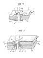
- the interposer 50 of the inventionis for making connections to a circuit board 80 (FIG. 2) having contact pads 81 .
- the contact padsinclude a portion extending radially outwardly from a hole 83 in the circuit panel.
- the contact padsmay further include a portion formed by plating the hole 83 with a conductive material.
- An edge 84is formed by the contact pad at the periphery of the hole 83 . In the contact pad shown in FIG. 2, the edge 84 is formed at the juncture of the portion of the pad extending radially outwardly from the hole and the portion plated within the hole.
- the circuit panel 80also includes circuitry interconnecting the contact pads 81 with each other or with external wiring.
- FIGS. 2 and 3A method of making a multilayer circuit according to the invention using the interposer 50 is represented in FIGS. 2 and 3.
- the interposeris stacked with one or more circuit panels, such as circuit panel 80 , so that the first surface 65 of the interposer body confronts a horizontally extensive surface 86 of the circuit panel.
- the compliant layer 62is on the first major surface 65 of the interposer body and lies between the body and the horizontally extensive surface 86 of the circuit panel.
- the contacts 70 of the interposersconfront the contact pads 81 on the circuit panel 80 .
- An additional circuit panel 92may be stacked on the other side of the interposer 50 , with horizontally extensive surface 96 of the circuit panel 92 confronting the second major surface 66 of the interposer body.
- the compliant layer 61is on the second major surface 66 of the interposer body and lies between the body and the horizontally extensive surface 96 of the circuit panel 92 .
- the contacts 90 of the interposerconfront the contact pads 95 .
- the stacked panels and interposerare then compressed vertically, as shown in FIG. 3 .
- the contacts 70 , 90are forcibly engaged with the contact pads 81 , 95 of the circuit panels.
- the contactsdeform so that the central portions 75 of the contacts enter the holes 83 defined by the contact pads.
- the peripheral portions 74 of the contactshave circumferences larger than the diameter of the holes 83 , so that the peripheral portions engage the contact pads 81 , 95 around the holes.
- the interposer 50 and the circuit panels 80 , 92are forced together, the peripheral portions 74 are forced vertically downward, toward the body 60 of the interposer, wiping the contact pads. Wiping is concentrated at the edges 84 of the holes.
- the compliant layer 62permits the peripheral portion 74 of the contact to deform in a downward direction toward the body 60 .
- the compliant layer 62yields in response to the bending of the peripheral portion 74 toward the body 60 .
- frictional heatis developed, which, in a preferred embodiment, frictionally welds the contact to the contact pad.
- frictional weldingcreates highly reliable mechanical and electrical connections between the interposer and the circuit panel.
- Possible metallurgies of the contact and contact pad for use in this constructioninclude, for example, gold-gold, gold-tin, gold-tin-lead, tin-tin-lead, tin-tin, gold-copper and copper-copper.
- the base 60 of the interposer 50must be sufficiently flexible to compensate for variations in planarity of the contact pads 81 of the circuit panel. Where no compliant layer such as layer 62 is used, the base must additionally be sufficiently deformable to permit deflection of the peripheral portions of the contacts into the base material.
- Examples of possible base interposer materialsinclude a polyimide bondply, a reinforced B-staged material, thermoplastic films and insulated metal core materials.
- the layer 62is a compliant layer that is also an adhesive.
- the adhesivemay be pressure-activatable, in which case the circuit panel 80 is bonded to the interposer 50 during the step of pressing those two elements together.
- the adhesivemay alternatively be a heat-activatable adhesive. In that case, the assembly is heated after the interposer and the circuit panel are pressed together in order to activate the adhesive and bond the two elements together.
- the circuit panel 80 and circuit panel 92are electrically interconnected by the through-conductor 72 after assembly.
- the contacts 70 , 90are integral with the through conductor 72 and form a continuous electrical path between the contact pads 81 and the contact pads 95 of the two circuit panels.
- the through conductor, as well as the hole in which it was formedextends perpendicular to the first major surface 65 of the body 60 of the interposer.
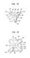
- the interposer 100has an array of contacts 70 arranged in a rectilinear grid, as shown in FIG. 4 .
- Each of the contacts 70has a non-circular periphery including tabs 73 .
- the tabs 73are arranged in a symmetrical pattern about the contact 70 ; in the embodiment shown in FIG. 4, four tabs are arranged in a quatrefoil pattern.
- the tabs 73extend from a central portion of the contact in a direction substantially diagonal to the rows and columns of the rectilinear grid.
- the rectilinear grid of contacts 70has a pitch 102 of approximately 1 mm (0.040 inches) The pitch is measured between similar features of adjacent contacts, such as a center-to-center distance.
- the interposer of the inventionmay be fabricated with pitches less than 1 mm in order to accommodate microelectronic components having greater contact densities. For example, an interposer having a contact grid array pitch of less than 1 mm is preferred; an interposer having a rectilinear array of contacts with a pitch of less than 0.75 mm (0.030 inches) is more preferred. An interposer having a contact pitch of less than 0.5 mm (0.020 inches) is most preferred.
- a contact arrayrequires process resolution considerably finer than the array pitch. For example, for an interposer having a contact pitch of 1 mm, holes in the circuit panels having a diameter of 0.4 mm (0.016 inches) are electroplated to 0.35 mm (0.014 inches) to form the central holes of the contact pads. Holes in the interposer having a diameter of 0.125 mm (0.005 inches) are electroplated to 0.1 mm (0.004 inches) to form the through conductors of the interposer.
- Contact arrays having finer pitchesrequire proportionally smaller feature sizes and process resolutions.
- a conductive bonding material 110may be provided for bonding the contact 70 to the contact pad of the circuit panel.
- the conductive bonding materialmay be a solder, a brazing alloy, a defusion bonding alloy, a polymer impregnated with conductive materials, or another activatable conductive bonding material. While shown on the contact 70 in the illustrative embodiment, the bonding material 110 may instead be present on the contact pad of the circuit panel, or may be applied to both the contact 70 and the contact pad.
- the bonding material 110is activated to form an electrical and mechanical bond between the contact pad and the contact.
- the bonding materialis activated by momentarily heating the assembly.
- flowable bonding materialsuch as solder
- the bonding materialbecomes temporarily flowable and wets the contact and contact pad.
- the contact materialresolidifies, forming a bond.
- momentary heating of the bonding materialmay cause chemical reactions, such as in the case of certain polymeric bonding materials and epoxy bonding materials.
- the step of momentarily heating the assemblymay not only activate the bonding material 110 between the contacts 70 and the contact pad of the circuit panel 10 , but also activate the adhesive layers 61 , 62 (FIGS. 2 - 3 ), forming a unitary structure including the interposer together with adjoining circuit panels.
- the step of momentarily heating the assemblymay also soften the material immediately below the peripheral portion 74 of the contact (FIG. 3 ), permitting the contacts to deform downwardly toward the body 60 as well as inwardly toward the conductor 72 when the peripheral portion 74 is engaged with a contact pad.
- a gap 115may be formed between the contact 70 and the first surface 65 of the interposer body 60 .
- a similar gap 116may be formed between the opposite surface 64 of the body 60 , and a second contact 90 . While the gaps are shown between the contacts and the interposer body, similar gaps may be provided between the contacts and the compliant or adhesive layers, where such layers are used.
- the gaps 115 , 116provide clearance for deformation of the peripheral portions 74 of the contacts 70 , 90 upon engagement with contact pads on circuit panels. By spacing the contacts above the surfaces of the interposer body, contact between the contacts and facing contact pads on the circuit panels is assured before the first surface 65 contacts the facing surface of the circuit panel. Furthermore, the gap 115 permits deformation of the periphery 74 of the contacts 70 without requiring a deformable material beneath the contacts 70 .
- the body 60need not necessarily be formed of a compressible or deformable material.
- the peripheral portion 74moves in a downward direction 121 toward the body 60 of the interposer, and in an inward direction 122 toward the conductor 72 .
- the edge 84 of the central hole 83 in the contact pad 81wipes along the surface of the contact 70 , breaking through oxidation layers to form a metal-to-metal contact between the contact pad 81 and the contact 70 .
- the wiping actionmay further induce friction welding or “cold” welding between those two components, forming a permanent mechanical bond. If an adhesive or other compliant layer 62 is present, that layer is deformed in the area around the peripheral region of the contact, as the contact is deformed downward and inward.
- the substantially cylindrical conductor 72is attached to the body 60 of the interposer and has sufficient rigidity so as to remain substantially undeformed during the engagement process.
- a vertical position 123 of the first end 71 of the conductor with respect to the first surface 65 of the interposer bodyremains substantially unchanged during the engagement.
- the first end 71 of the conductor 72thereby enters the hole 83 , dragging the peripheral portion 74 of the contact 70 across the edge 84 of the hole.
- the contact 70comprises a plurality of tabs such as tabs 73 (FIG. 6 )
- forces between the tabs and the edge 84 of the contact pad holeare concentrated at the edges 125 of the tabs.
- the edges 125 of the tabstherefore wipe the edge 84 of the contact pad hole with relatively great force, removing oxide layers in that area and promoting cold welding.
- the conductor 72may have an increased wall thickness as compared to the contact 70 . Further, the closed cylindrical shape of the conductor 72 creates a column-like structure that is resistant to compressive forces during contact engagement. Other shapes known to be resistant to compressive column loads, such as a triangular box beam, may be used.
- the contact 70may be formed directly on a primary surface 165 of an interposer body 160 (FIG. 8 ).
- the interposer body 160must be deformable in order to permit the contacts 70 to deform downwardly and inwardly upon engagement with opposing contact pads. While an entire interposer body may be fabricated from a uniformly compliant material, such an approach is not practical with certain materials because of the strength requirement of the interposer in areas between contacts. Another solution is to provide a compliant region 168 in the interposer 160 in a local area beneath the contact 70 .
- Such a regionmay be formed by using an initially b-staged material for forming the body 160 , then forming the contacts on the body and finally curing the body 160 in all areas other than those beneath the contacts 170 .
- Such selective curingmay be done by radiation curing with a mask (not shown) blocking the areas around the contacts, or by using the contacts 170 themselves as a mask during curing.
- the thickness of an adhesive layer 162may be increased in the area surrounding the contact 70 in order to provide support for the contact during transport and handling of the interposer.
- the compliant layer 162comprises a region of smaller thickness 164 in an area remote from contacts 70 and a region of increased thickness 163 directly beneath the contacts 70 .
- the region 163provides support for the contact during handling.
- the area of decreased thickness 164permits the contact 70 to contact the contact pads of the circuit panel, and assure complete contact before the top surface of the adhesive or compliant layer 162 contacts the facing surface of the circuit panel.
- the interposer bodyitself may have areas of reduced thickness in regions between contacts. In either case, the regions of reduced thickness may be formed using a plasma etching process, wherein the contact itself acts as a mask, preventing etching of the material directly below.
- Contact tabs 178may be provided with asperities 179 on their upper surfaces in order to enhance wiping action between the tabs and the mating contact pads on the circuit panels.
- the asperitiesmay be formed by selectively etching the top surfaces of the tabs.
- the asperitiesmay be provided on the facing surfaces of the contact pads. In either case, the asperities break through the oxidation layers on the opposing surfaces, forming metal-to-metal contact.
- the contacts of the present inventionare highly tolerant of size and/or positional errors in the contacts themselves and in mating contact pads.
- a contact 270 having tabs 273may be used with a contact pad having a large hole-size tolerance, represented by circles 280 , 281 .
- the edge formed by either hole 280 , 281is wiped by the four tabs 273 during engagement, removing oxidation and forming a metal-to-metal contact.
- contact engagementis not excessively affected by hole size.
- Contact engagement according to the inventionis also robust with regard to positional tolerances affecting the relative positions of the contact and the corresponding contact pad.
- a contact 270 having four tabs 273may effectively engage contact pads with a wide range of positions, represented by holes 283 - 286 . While positional deviation will result in some tabs 273 being deformed to a greater degree than others in a single contact, the design permits variations in relative position without substantially affecting the overall mechanical and electrical performance of the joint.
- a contact pad 291 (FIG. 13A) of a circuit panelmay have a polygonal hole, such as square hole 294 . Such a hole presents multiple surfaces for wiping the contact as it is inserted.
- a contact 292 (FIG. 13B) having a circular periphery 295may be used in conjunction with the square hole 294 .
- a conductor connected to the central portion 293has a sufficiently small diameter to clear the square hole 294 , given positional and size tolerances as illustrated in FIGS. 11 and 12.
- the relative sizes of the periphery 295 of the contact and the square hole 294 of the contact pad 291are selected so as to contact a plurality of substantially separate edge portions 296 (FIG. 13C) of the contact 292 . It is believed that the edge portions “fold” downward and inward as the contact and contact pad engage. That configuration permits the use of the circular periphery 295 without resulting in excessive engagement forces. In contrast, full engagement around the periphery of a circular contact does not permit “folding” of such edge portions, and thus results in high engagement forces.
- a circular contact periphery 295is desirable in the manufacture of smaller pitch sizes, because of the limitations in the photolithographic process.
- a tabbed contact 310may also be used in conjunction with a polygonal hole 320 in a contact pad.
- a contact having three tabs 312may be inserted in a triangular hole 320 having edges 322 forming vertices 321 .
- the tabs 312are aligned with the vertices 321 , forming two primary contact points 314 on each tab 312 between the tab edges 313 and the edges 322 of the triangular hole. Localized contact at the contact points 314 results in high contact stresses with increased wiping and increased cold welding.
- the tabs 332may have a circumferential width 341 near the tips that is greater than the circumferential width 340 near the central portion 339 .
- the contact points 334 between the tab edges 333 and the edges 342 of the contact pad hole 345move along the contact pad hole edges 342 as the contact is inserted into the hole.
- the photolithographic process used in forming the contactsmay be used to create a wide variety of contact geometries. For example, as shown in FIGS. 16A-16C, the number of tabs in a multiple-tabbed configuration may be reduced to form a three-tabbed contact 410 , a two-tabbed contact 412 or a one-tabbed contact 413 . A reduced number of tabs requires less resolution in the photolithographic process by permitting the formation of wider tabs, which are less likely to be lost during imaging.
- Star-shaped configurationssuch as those shown in FIGS. 16D-16G, have points 415 on the tips of the tabs. Where the contact is completely pressed into the hole in the contact pad, the points 415 scrape the inside wall of the hole, improving the mechanical and electrical connection.
- the scraping of the tips of the tabs within a contact pad holemay be enhanced by providing multiple points 416 (FIG. 16H) on the tabs.
- the relatively large number of tabs in a star-shaped configurationprovide multiple conductive pathways between the contact and the contact pad. Such multiple pathways make the joints less sensitive to the loss of tabs in the photolithographic process, as well to defective joints between a tab and the mating contact pad.
- a contact 420(FIG. 16I) having a large number of tabs provides a large number of electrical paths between the contact and the contact pad.
- Such a contactmay form a substantially continuous conical shape upon insertion into a contact pad hole, providing the maximum cross-sectional conductive area between the interposer and the circuit panel.
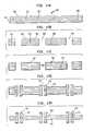
- an initial laminateis first formed.
- a polyimide body 560(FIG. 17A) is first coated with a compliant adhesive 561 , 562 .
- the adhesivemay be a thermoplastic or b-staged adhesive, and is preferably a thermoplastic.
- the adhesiveis selected from the group consisting of polyetherimide (PEI) and polyimide.
- PEIpolyetherimide
- the adhesiveis applied to both surfaces of the body 560 .
- the adhesivemay be applied by transfer lamination, or by mechanically or chemically coating the polyimide sheet with a layer of adhesive.
- Sacrificial metallic layers 550 , 551are next applied to the exposed surfaces of the adhesive.
- the metallic layersare formed of a material selected to be chemically removable without removing the contacts and conductors formed later in the process.
- a preferred sacrificial layer materialis aluminum.
- Through holes 565are next formed in the resulting laminate.
- the through holesmay be drilled, such as by laser ablation, or may be punched or otherwise formed in the laminate.
- the holesextend completely through the base layer 560 , the adhesive layers 561 , 562 and the sacrificial layers 550 , 551 .
- the entire assemblyis next sputter metalized to form a flash metallic layer 567 (FIG. 17 C).
- the flash metallic layer 567is preferably gold, but may alternatively be tin, copper or another metal compatible with the materials used in the contact and conductor-forming processes.
- the metalization processforms a layer on the exposed surfaces of the sacrificial layer 550 , 551 , as well as within the holes 565 .
- the contacts 570 and conductors 572are next formed in the holes.
- the contacts and conductorsare preferably formed integrally by first forming patterned photoresist layers (not shown) defining the outer periphery of the contacts on the flash coated outer surfaces of the sacrificial layers 550 , 551 .
- the contacts 570 , 572are then formed by electroplating the contact material onto the areas not covered with photoresist.
- the contact materialis then plated with a gold or tin finish layer 575 , and the photoresist pattern layers are removed.
- the sacrificial aluminum layers 550 , 551are then removed using an etchant that leaves the contacts 570 and conductors 572 substantially intact.
- the removal of the sacrificial layersleaves a gap 515 between the contact 570 and the adhesive layer 562 . That gap permits deformation of the contact 570 upon engagement with a contact pad on a mating circuit panel. Because the contacts 570 are spaced away from the outer surface of the adhesive 562 , full engagement of the contacts with contact pads is assured before engagement of the adhesive 562 with the facing surface of the circuit panel.
- the above method of fabricating an interposer according to the inventionmay be performed without applying a sacrificial layer on the adhesive.
- the contactsare formed directly over the adhesive layer.
- the adhesive layeris formed of a material selected to be compliant in order to permit the contact 570 to deflect downward and inward into the adhesive layer.
- the methodwas described as including an adhesive layer, that layer may be replaced by another compliant layer that does not necessarily adhere to the circuit panel.
- the compliant layer or adhesive layermay be completely eliminated, either forming the contact 570 spaced away from the body 560 to permit deformation, or using an at least locally compliant body 560 to permit deformation of the contacts into the body.
Landscapes
- Engineering & Computer Science (AREA)
- Microelectronics & Electronic Packaging (AREA)
- Manufacturing & Machinery (AREA)
- Physics & Mathematics (AREA)
- Condensed Matter Physics & Semiconductors (AREA)
- General Physics & Mathematics (AREA)
- Computer Hardware Design (AREA)
- Power Engineering (AREA)
- Coupling Device And Connection With Printed Circuit (AREA)
Abstract
Description
Claims (28)
Priority Applications (4)
| Application Number | Priority Date | Filing Date | Title |
|---|---|---|---|
| US09/779,117US6700072B2 (en) | 1996-12-13 | 2001-02-08 | Electrical connection with inwardly deformable contacts |
| US10/200,941US6706973B2 (en) | 1996-12-13 | 2002-07-23 | Electrical connection with inwardly deformable contacts |
| US10/658,941US6978538B2 (en) | 1996-12-13 | 2003-09-10 | Method for making a microelectronic interposer |
| US11/211,810US20060040522A1 (en) | 1996-12-13 | 2005-08-25 | Method for making a microelectronic interposer |
Applications Claiming Priority (3)
| Application Number | Priority Date | Filing Date | Title |
|---|---|---|---|
| US3288496P | 1996-12-13 | 1996-12-13 | |
| US08/989,305US6247228B1 (en) | 1996-08-12 | 1997-12-12 | Electrical connection with inwardly deformable contacts |
| US09/779,117US6700072B2 (en) | 1996-12-13 | 2001-02-08 | Electrical connection with inwardly deformable contacts |
Related Parent Applications (1)
| Application Number | Title | Priority Date | Filing Date |
|---|---|---|---|
| US08/989,305DivisionUS6247228B1 (en) | 1996-08-12 | 1997-12-12 | Electrical connection with inwardly deformable contacts |
Related Child Applications (1)
| Application Number | Title | Priority Date | Filing Date |
|---|---|---|---|
| US10/200,941DivisionUS6706973B2 (en) | 1996-12-13 | 2002-07-23 | Electrical connection with inwardly deformable contacts |
Publications (2)
| Publication Number | Publication Date |
|---|---|
| US20010011605A1 US20010011605A1 (en) | 2001-08-09 |
| US6700072B2true US6700072B2 (en) | 2004-03-02 |
Family
ID=26709011
Family Applications (5)
| Application Number | Title | Priority Date | Filing Date |
|---|---|---|---|
| US08/989,305Expired - LifetimeUS6247228B1 (en) | 1996-08-12 | 1997-12-12 | Electrical connection with inwardly deformable contacts |
| US09/779,117Expired - LifetimeUS6700072B2 (en) | 1996-12-13 | 2001-02-08 | Electrical connection with inwardly deformable contacts |
| US10/200,941Expired - LifetimeUS6706973B2 (en) | 1996-12-13 | 2002-07-23 | Electrical connection with inwardly deformable contacts |
| US10/658,941Expired - Fee RelatedUS6978538B2 (en) | 1996-12-13 | 2003-09-10 | Method for making a microelectronic interposer |
| US11/211,810AbandonedUS20060040522A1 (en) | 1996-12-13 | 2005-08-25 | Method for making a microelectronic interposer |
Family Applications Before (1)
| Application Number | Title | Priority Date | Filing Date |
|---|---|---|---|
| US08/989,305Expired - LifetimeUS6247228B1 (en) | 1996-08-12 | 1997-12-12 | Electrical connection with inwardly deformable contacts |
Family Applications After (3)
| Application Number | Title | Priority Date | Filing Date |
|---|---|---|---|
| US10/200,941Expired - LifetimeUS6706973B2 (en) | 1996-12-13 | 2002-07-23 | Electrical connection with inwardly deformable contacts |
| US10/658,941Expired - Fee RelatedUS6978538B2 (en) | 1996-12-13 | 2003-09-10 | Method for making a microelectronic interposer |
| US11/211,810AbandonedUS20060040522A1 (en) | 1996-12-13 | 2005-08-25 | Method for making a microelectronic interposer |
Country Status (1)
| Country | Link |
|---|---|
| US (5) | US6247228B1 (en) |
Cited By (27)
| Publication number | Priority date | Publication date | Assignee | Title |
|---|---|---|---|---|
| US20040045159A1 (en)* | 1996-12-13 | 2004-03-11 | Tessera, Inc. | Electrical connection with inwardly deformable contacts |
| US20040252477A1 (en)* | 2003-06-11 | 2004-12-16 | Brown Dirk D. | Contact grid array formed on a printed circuit board |
| US20050124181A1 (en)* | 2003-12-08 | 2005-06-09 | Brown Dirk D. | Connector for making electrical contact at semiconductor scales |
| US20050120553A1 (en)* | 2003-12-08 | 2005-06-09 | Brown Dirk D. | Method for forming MEMS grid array connector |
| US20050164527A1 (en)* | 2003-04-11 | 2005-07-28 | Radza Eric M. | Method and system for batch forming spring elements in three dimensions |
| US20050208788A1 (en)* | 2004-03-19 | 2005-09-22 | Dittmann Larry E | Electrical connector in a flexible host |
| US20050208787A1 (en)* | 2004-03-19 | 2005-09-22 | Epic Technology Inc. | Interposer with compliant pins |
| US20050208786A1 (en)* | 2004-03-19 | 2005-09-22 | Epic Technology Inc. | Interposer and method for making same |
| US20050205988A1 (en)* | 2004-03-19 | 2005-09-22 | Epic Technology Inc. | Die package with higher useable die contact pad area |
| US20050227510A1 (en)* | 2004-04-09 | 2005-10-13 | Brown Dirk D | Small array contact with precision working range |
| US20060000642A1 (en)* | 2004-07-01 | 2006-01-05 | Epic Technology Inc. | Interposer with compliant pins |
| US7056131B1 (en) | 2003-04-11 | 2006-06-06 | Neoconix, Inc. | Contact grid array system |
| US20060258182A1 (en)* | 2004-07-20 | 2006-11-16 | Dittmann Larry E | Interposer with compliant pins |
| US20060258183A1 (en)* | 2003-04-11 | 2006-11-16 | Neoconix, Inc. | Electrical connector on a flexible carrier |
| US20070050738A1 (en)* | 2005-08-31 | 2007-03-01 | Dittmann Larry E | Customer designed interposer |
| US20070054515A1 (en)* | 2003-04-11 | 2007-03-08 | Williams John D | Method for fabricating a contact grid array |
| US20070134949A1 (en)* | 2005-12-12 | 2007-06-14 | Dittmann Larry E | Connector having staggered contact architecture for enhanced working range |
| US20070141863A1 (en)* | 2003-04-11 | 2007-06-21 | Williams John D | Contact grid array system |
| US20070218710A1 (en)* | 2003-06-11 | 2007-09-20 | Brown Dirk D | Structure and process for a contact grid array formed in a circuitized substrate |
| US20070259539A1 (en)* | 2003-04-11 | 2007-11-08 | Brown Dirk D | Method and system for batch manufacturing of spring elements |
| US7347698B2 (en) | 2004-03-19 | 2008-03-25 | Neoconix, Inc. | Deep drawn electrical contacts and method for making |
| US20080099232A1 (en)* | 2006-10-25 | 2008-05-01 | Silicon Test Systems, Inc. | Three-dimensional printed circuit board for use with electronic circuitry |
| US20100167561A1 (en)* | 2003-04-11 | 2010-07-01 | Neoconix, Inc. | Structure and process for a contact grid array formed in a circuitized substrate |
| US7914296B1 (en)* | 2010-01-05 | 2011-03-29 | Exatron, Inc. | Interconnecting assembly with conductive lever portions on a support film |
| CN102281703A (en)* | 2010-06-09 | 2011-12-14 | 富士通株式会社 | Laminated circuit board and board producing method |
| US8641428B2 (en) | 2011-12-02 | 2014-02-04 | Neoconix, Inc. | Electrical connector and method of making it |
| US9680273B2 (en) | 2013-03-15 | 2017-06-13 | Neoconix, Inc | Electrical connector with electrical contacts protected by a layer of compressible material and method of making it |
Families Citing this family (82)
| Publication number | Priority date | Publication date | Assignee | Title |
|---|---|---|---|---|
| US5484959A (en)* | 1992-12-11 | 1996-01-16 | Staktek Corporation | High density lead-on-package fabrication method and apparatus |
| US6204065B1 (en)* | 1997-03-27 | 2001-03-20 | Ngk Insulators, Ltd. | Conduction assist member and manufacturing method of the same |
| US6713685B1 (en)* | 1998-09-10 | 2004-03-30 | Viasystems Group, Inc. | Non-circular micro-via |
| US6323060B1 (en) | 1999-05-05 | 2001-11-27 | Dense-Pac Microsystems, Inc. | Stackable flex circuit IC package and method of making same |
| JP4034483B2 (en)* | 1999-09-24 | 2008-01-16 | 東光株式会社 | Manufacturing method of multilayer chip component |
| US6262895B1 (en) | 2000-01-13 | 2001-07-17 | John A. Forthun | Stackable chip package with flex carrier |
| US6460170B1 (en)* | 2000-04-29 | 2002-10-01 | Hewlett Packard Company | Connection block for interfacing a plurality of printed circuit boards |
| WO2003010813A2 (en)* | 2001-07-23 | 2003-02-06 | Clayton Gary A | Grid interposer |
| US6633489B2 (en)* | 2001-07-31 | 2003-10-14 | Hewlett-Packard Development Company, L.P. | Dynamic isolating mount for processor packages |
| US20040195666A1 (en)* | 2001-10-26 | 2004-10-07 | Julian Partridge | Stacked module systems and methods |
| US6914324B2 (en)* | 2001-10-26 | 2005-07-05 | Staktek Group L.P. | Memory expansion and chip scale stacking system and method |
| US20050009234A1 (en)* | 2001-10-26 | 2005-01-13 | Staktek Group, L.P. | Stacked module systems and methods for CSP packages |
| US7371609B2 (en)* | 2001-10-26 | 2008-05-13 | Staktek Group L.P. | Stacked module systems and methods |
| US20060255446A1 (en) | 2001-10-26 | 2006-11-16 | Staktek Group, L.P. | Stacked modules and method |
| US7485951B2 (en)* | 2001-10-26 | 2009-02-03 | Entorian Technologies, Lp | Modularized die stacking system and method |
| US6956284B2 (en) | 2001-10-26 | 2005-10-18 | Staktek Group L.P. | Integrated circuit stacking system and method |
| US6940729B2 (en) | 2001-10-26 | 2005-09-06 | Staktek Group L.P. | Integrated circuit stacking system and method |
| US7310458B2 (en) | 2001-10-26 | 2007-12-18 | Staktek Group L.P. | Stacked module systems and methods |
| US7053478B2 (en)* | 2001-10-26 | 2006-05-30 | Staktek Group L.P. | Pitch change and chip scale stacking system |
| US6576992B1 (en)* | 2001-10-26 | 2003-06-10 | Staktek Group L.P. | Chip scale stacking system and method |
| US7202555B2 (en)* | 2001-10-26 | 2007-04-10 | Staktek Group L.P. | Pitch change and chip scale stacking system and method |
| US7026708B2 (en)* | 2001-10-26 | 2006-04-11 | Staktek Group L.P. | Low profile chip scale stacking system and method |
| US20050056921A1 (en)* | 2003-09-15 | 2005-03-17 | Staktek Group L.P. | Stacked module systems and methods |
| US20030234443A1 (en) | 2001-10-26 | 2003-12-25 | Staktek Group, L.P. | Low profile stacking system and method |
| US7656678B2 (en) | 2001-10-26 | 2010-02-02 | Entorian Technologies, Lp | Stacked module systems |
| US7081373B2 (en)* | 2001-12-14 | 2006-07-25 | Staktek Group, L.P. | CSP chip stack with flex circuit |
| TWI286826B (en)* | 2001-12-28 | 2007-09-11 | Via Tech Inc | Semiconductor package substrate and process thereof |
| US7754976B2 (en)* | 2002-04-15 | 2010-07-13 | Hamilton Sundstrand Corporation | Compact circuit carrier package |
| US6828513B2 (en)* | 2002-04-30 | 2004-12-07 | Texas Instruments Incorporated | Electrical connector pad assembly for printed circuit board |
| JP3879651B2 (en)* | 2002-10-21 | 2007-02-14 | ソニー株式会社 | Multilayer wiring board, touch panel, and manufacturing method thereof |
| US7265045B2 (en)* | 2002-10-24 | 2007-09-04 | Megica Corporation | Method for fabricating thermal compliant semiconductor chip wiring structure for chip scale packaging |
| DE10258094B4 (en) | 2002-12-11 | 2009-06-18 | Qimonda Ag | Method of forming 3-D structures on wafers |
| US20040245615A1 (en)* | 2003-06-03 | 2004-12-09 | Staktek Group, L.P. | Point to point memory expansion system and method |
| US7042080B2 (en)* | 2003-07-14 | 2006-05-09 | Micron Technology, Inc. | Semiconductor interconnect having compliant conductive contacts |
| US7542304B2 (en)* | 2003-09-15 | 2009-06-02 | Entorian Technologies, Lp | Memory expansion and integrated circuit stacking system and method |
| US20050128948A1 (en)* | 2003-12-11 | 2005-06-16 | Chen-Chi Kuo | Locally stored portion of a calendar structure indicating when interfaces will become available to transmit packets |
| US9097740B2 (en)* | 2004-05-21 | 2015-08-04 | Formfactor, Inc. | Layered probes with core |
| US7659739B2 (en)* | 2006-09-14 | 2010-02-09 | Micro Porbe, Inc. | Knee probe having reduced thickness section for control of scrub motion |
| USRE43503E1 (en) | 2006-06-29 | 2012-07-10 | Microprobe, Inc. | Probe skates for electrical testing of convex pad topologies |
| US7759949B2 (en)* | 2004-05-21 | 2010-07-20 | Microprobe, Inc. | Probes with self-cleaning blunt skates for contacting conductive pads |
| US9476911B2 (en) | 2004-05-21 | 2016-10-25 | Microprobe, Inc. | Probes with high current carrying capability and laser machining methods |
| US8988091B2 (en) | 2004-05-21 | 2015-03-24 | Microprobe, Inc. | Multiple contact probes |
| US7733101B2 (en)* | 2004-05-21 | 2010-06-08 | Microprobe, Inc. | Knee probe having increased scrub motion |
| US20060033187A1 (en)* | 2004-08-12 | 2006-02-16 | Staktek Group, L.P. | Rugged CSP module system and method |
| US20060043558A1 (en)* | 2004-09-01 | 2006-03-02 | Staktek Group L.P. | Stacked integrated circuit cascade signaling system and method |
| US20060055024A1 (en)* | 2004-09-14 | 2006-03-16 | Staktek Group, L.P. | Adapted leaded integrated circuit module |
| US20060072297A1 (en)* | 2004-10-01 | 2006-04-06 | Staktek Group L.P. | Circuit Module Access System and Method |
| US20060118936A1 (en)* | 2004-12-03 | 2006-06-08 | Staktek Group L.P. | Circuit module component mounting system and method |
| US7309914B2 (en)* | 2005-01-20 | 2007-12-18 | Staktek Group L.P. | Inverted CSP stacking system and method |
| US20060244114A1 (en)* | 2005-04-28 | 2006-11-02 | Staktek Group L.P. | Systems, methods, and apparatus for connecting a set of contacts on an integrated circuit to a flex circuit via a contact beam |
| US7033861B1 (en) | 2005-05-18 | 2006-04-25 | Staktek Group L.P. | Stacked module systems and method |
| TW200644261A (en)* | 2005-06-06 | 2006-12-16 | Megica Corp | Chip-package structure and manufacturing process thereof |
| US7331796B2 (en)* | 2005-09-08 | 2008-02-19 | International Business Machines Corporation | Land grid array (LGA) interposer utilizing metal-on-elastomer hemi-torus and other multiple points of contact geometries |
| US7576995B2 (en) | 2005-11-04 | 2009-08-18 | Entorian Technologies, Lp | Flex circuit apparatus and method for adding capacitance while conserving circuit board surface area |
| US7649367B2 (en) | 2005-12-07 | 2010-01-19 | Microprobe, Inc. | Low profile probe having improved mechanical scrub and reduced contact inductance |
| US7304382B2 (en) | 2006-01-11 | 2007-12-04 | Staktek Group L.P. | Managed memory component |
| US7605454B2 (en) | 2006-01-11 | 2009-10-20 | Entorian Technologies, Lp | Memory card and method for devising |
| US7608920B2 (en) | 2006-01-11 | 2009-10-27 | Entorian Technologies, Lp | Memory card and method for devising |
| US7508058B2 (en) | 2006-01-11 | 2009-03-24 | Entorian Technologies, Lp | Stacked integrated circuit module |
| US7508069B2 (en) | 2006-01-11 | 2009-03-24 | Entorian Technologies, Lp | Managed memory component |
| US7312617B2 (en) | 2006-03-20 | 2007-12-25 | Microprobe, Inc. | Space transformers employing wire bonds for interconnections with fine pitch contacts |
| US7746661B2 (en)* | 2006-06-08 | 2010-06-29 | Sandisk Corporation | Printed circuit board with coextensive electrical connectors and contact pad areas |
| US7786740B2 (en)* | 2006-10-11 | 2010-08-31 | Astria Semiconductor Holdings, Inc. | Probe cards employing probes having retaining portions for potting in a potting region |
| US8907689B2 (en)* | 2006-10-11 | 2014-12-09 | Microprobe, Inc. | Probe retention arrangement |
| US7468553B2 (en) | 2006-10-20 | 2008-12-23 | Entorian Technologies, Lp | Stackable micropackages and stacked modules |
| JP2008108890A (en)* | 2006-10-25 | 2008-05-08 | Three M Innovative Properties Co | Adhesion method for circuit board and adhesion structure body |
| US7417310B2 (en) | 2006-11-02 | 2008-08-26 | Entorian Technologies, Lp | Circuit module having force resistant construction |
| US7514948B2 (en) | 2007-04-10 | 2009-04-07 | Microprobe, Inc. | Vertical probe array arranged to provide space transformation |
| US7671610B2 (en)* | 2007-10-19 | 2010-03-02 | Microprobe, Inc. | Vertical guided probe array providing sideways scrub motion |
| US8723546B2 (en)* | 2007-10-19 | 2014-05-13 | Microprobe, Inc. | Vertical guided layered probe |
| US20090146295A1 (en)* | 2007-12-11 | 2009-06-11 | Hidefumi Narita | Ceramic substrate having thermal via |
| US8230593B2 (en)* | 2008-05-29 | 2012-07-31 | Microprobe, Inc. | Probe bonding method having improved control of bonding material |
| US7808258B2 (en)* | 2008-06-26 | 2010-10-05 | Freescale Semiconductor, Inc. | Test interposer having active circuit component and method therefor |
| US8073019B2 (en)* | 2009-03-02 | 2011-12-06 | Jian Liu | 810 nm ultra-short pulsed fiber laser |
| GB2469115B (en)* | 2009-04-03 | 2013-08-21 | Keronite Internat Ltd | Process for the enhanced corrosion protection of valve metals |
| JP5593863B2 (en)* | 2010-06-09 | 2014-09-24 | 富士通株式会社 | Multilayer circuit board and substrate manufacturing method |
| TWI527174B (en)* | 2010-11-19 | 2016-03-21 | 日月光半導體製造股份有限公司 | Package having semiconductor device |
| JP5533596B2 (en)* | 2010-11-25 | 2014-06-25 | 富士通株式会社 | Printed wiring board manufacturing method, printed wiring board, and electronic device |
| US10750614B2 (en)* | 2017-06-12 | 2020-08-18 | Invensas Corporation | Deformable electrical contacts with conformable target pads |
| CN107155266B (en)* | 2017-06-20 | 2020-10-23 | 广州兴森快捷电路科技有限公司 | Z-direction interconnection circuit board and manufacturing method thereof |
| CN108111138B (en)* | 2017-12-27 | 2021-06-15 | 安徽华东光电技术研究所 | Method for manufacturing power amplifier |
| CN116600469B (en)* | 2023-07-17 | 2023-09-22 | 北京三重华星电子科技有限公司 | Printed circuit board with soldered electronic components |
Citations (43)
| Publication number | Priority date | Publication date | Assignee | Title |
|---|---|---|---|---|
| US3190953A (en) | 1961-06-15 | 1965-06-22 | Martin Marietta Corp | Channel flanged capillary eyelet for printed circuit boards |
| US3316619A (en) | 1963-12-09 | 1967-05-02 | Rca Corp | Method of making connections to stacked printed circuit boards |
| US3316618A (en) | 1963-12-09 | 1967-05-02 | Rca Corp | Method of making connection to stacked printed circuit boards |
| US3509270A (en) | 1968-04-08 | 1970-04-28 | Ney Co J M | Interconnection for printed circuits and method of making same |
| US3541222A (en) | 1969-01-13 | 1970-11-17 | Bunker Ramo | Connector screen for interconnecting adjacent surfaces of laminar circuits and method of making |
| US3616532A (en) | 1970-02-02 | 1971-11-02 | Sperry Rand Corp | Multilayer printed circuit electrical interconnection device |
| US3739469A (en) | 1971-12-27 | 1973-06-19 | Ibm | Multilayer printed circuit board and method of manufacture |
| US3795037A (en) | 1970-05-05 | 1974-03-05 | Int Computers Ltd | Electrical connector devices |
| US3862790A (en) | 1971-07-22 | 1975-01-28 | Plessey Handel Investment Ag | Electrical interconnectors and connector assemblies |
| US3904934A (en) | 1973-03-26 | 1975-09-09 | Massachusetts Inst Technology | Interconnection of planar electronic structures |
| US4074342A (en) | 1974-12-20 | 1978-02-14 | International Business Machines Corporation | Electrical package for lsi devices and assembly process therefor |
| US4225900A (en) | 1978-10-25 | 1980-09-30 | Raytheon Company | Integrated circuit device package interconnect means |
| US4249302A (en) | 1978-12-28 | 1981-02-10 | Ncr Corporation | Multilayer printed circuit board |
| US4528072A (en) | 1979-05-24 | 1985-07-09 | Fujitsu Limited | Process for manufacturing hollow multilayer printed wiring board |
| US4548451A (en) | 1984-04-27 | 1985-10-22 | International Business Machines Corporation | Pinless connector interposer and method for making the same |
| US4655519A (en) | 1985-10-16 | 1987-04-07 | Amp Incorporated | Electrical connector for interconnecting arrays of conductive areas |
| US4685210A (en) | 1985-03-13 | 1987-08-11 | The Boeing Company | Multi-layer circuit board bonding method utilizing noble metal coated surfaces |
| US4695870A (en) | 1986-03-27 | 1987-09-22 | Hughes Aircraft Company | Inverted chip carrier |
| US4716049A (en) | 1985-12-20 | 1987-12-29 | Hughes Aircraft Company | Compressive pedestal for microminiature connections |
| US4729809A (en) | 1985-03-14 | 1988-03-08 | Amp Incorporated | Anisotropically conductive adhesive composition |
| US4788766A (en) | 1987-05-20 | 1988-12-06 | Loral Corporation | Method of fabricating a multilayer circuit board assembly |
| US4793814A (en) | 1986-07-21 | 1988-12-27 | Rogers Corporation | Electrical circuit board interconnect |
| US4902606A (en) | 1985-12-20 | 1990-02-20 | Hughes Aircraft Company | Compressive pedestal for microminiature connections |
| US4924353A (en) | 1985-12-20 | 1990-05-08 | Hughes Aircraft Company | Connector system for coupling to an integrated circuit chip |
| US4954878A (en) | 1989-06-29 | 1990-09-04 | Digital Equipment Corp. | Method of packaging and powering integrated circuit chips and the chip assembly formed thereby |
| US5037312A (en) | 1990-11-15 | 1991-08-06 | Amp Incorporated | Conductive gel area array connector |
| US5047830A (en) | 1990-05-22 | 1991-09-10 | Amp Incorporated | Field emitter array integrated circuit chip interconnection |
| US5129142A (en) | 1990-10-30 | 1992-07-14 | International Business Machines Corporation | Encapsulated circuitized power core alignment and lamination |
| US5131852A (en) | 1991-08-23 | 1992-07-21 | Amp Incorporated | Electrical socket |
| US5142775A (en) | 1990-10-30 | 1992-09-01 | International Business Machines Corporation | Bondable via |
| US5152695A (en) | 1991-10-10 | 1992-10-06 | Amp Incorporated | Surface mount electrical connector |
| US5167512A (en) | 1991-07-05 | 1992-12-01 | Walkup William B | Multi-chip module connector element and system |
| US5173055A (en) | 1991-08-08 | 1992-12-22 | Amp Incorporated | Area array connector |
| US5224265A (en) | 1991-10-29 | 1993-07-06 | International Business Machines Corporation | Fabrication of discrete thin film wiring structures |
| US5228861A (en) | 1992-06-12 | 1993-07-20 | Amp Incorporated | High density electrical connector system |
| US5232548A (en) | 1991-10-29 | 1993-08-03 | International Business Machines Corporation | Discrete fabrication of multi-layer thin film, wiring structures |
| US5282312A (en) | 1991-12-31 | 1994-02-01 | Tessera, Inc. | Multi-layer circuit construction methods with customization features |
| US5430614A (en) | 1990-02-14 | 1995-07-04 | Particle Interconnect Inc. | Electrical interconnect using particle enhanced joining of metal surfaces |
| US5432677A (en) | 1993-02-09 | 1995-07-11 | Texas Instruments Incorporated | Multi-chip integrated circuit module |
| US5590460A (en) | 1994-07-19 | 1997-01-07 | Tessera, Inc. | Method of making multilayer circuit |
| US5632631A (en) | 1994-06-07 | 1997-05-27 | Tessera, Inc. | Microelectronic contacts with asperities and methods of making same |
| US5666270A (en) | 1993-10-18 | 1997-09-09 | Fujitsu Limited | Bump electrode, semiconductor integrated circuit device using the same, multi-chip module having the semiconductor integrated circuit devices and method for producing semicondutcor device having the bump electrode |
| US5736679A (en) | 1995-12-26 | 1998-04-07 | International Business Machines Corporation | Deformable interconnect structure for connecting an internal plane to a through-hole in a multilayer circuit board |
Family Cites Families (2)
| Publication number | Priority date | Publication date | Assignee | Title |
|---|---|---|---|---|
| DE4013077A1 (en)* | 1990-04-25 | 1991-10-31 | Hoechst Ag | METHOD FOR GLYCOSIDASE-CATALYZED SYNTHESIS OF GLYCO-CONJUGATES |
| US6247228B1 (en)* | 1996-08-12 | 2001-06-19 | Tessera, Inc. | Electrical connection with inwardly deformable contacts |
- 1997
- 1997-12-12USUS08/989,305patent/US6247228B1/ennot_activeExpired - Lifetime
- 2001
- 2001-02-08USUS09/779,117patent/US6700072B2/ennot_activeExpired - Lifetime
- 2002
- 2002-07-23USUS10/200,941patent/US6706973B2/ennot_activeExpired - Lifetime
- 2003
- 2003-09-10USUS10/658,941patent/US6978538B2/ennot_activeExpired - Fee Related
- 2005
- 2005-08-25USUS11/211,810patent/US20060040522A1/ennot_activeAbandoned
Patent Citations (43)
| Publication number | Priority date | Publication date | Assignee | Title |
|---|---|---|---|---|
| US3190953A (en) | 1961-06-15 | 1965-06-22 | Martin Marietta Corp | Channel flanged capillary eyelet for printed circuit boards |
| US3316619A (en) | 1963-12-09 | 1967-05-02 | Rca Corp | Method of making connections to stacked printed circuit boards |
| US3316618A (en) | 1963-12-09 | 1967-05-02 | Rca Corp | Method of making connection to stacked printed circuit boards |
| US3509270A (en) | 1968-04-08 | 1970-04-28 | Ney Co J M | Interconnection for printed circuits and method of making same |
| US3541222A (en) | 1969-01-13 | 1970-11-17 | Bunker Ramo | Connector screen for interconnecting adjacent surfaces of laminar circuits and method of making |
| US3616532A (en) | 1970-02-02 | 1971-11-02 | Sperry Rand Corp | Multilayer printed circuit electrical interconnection device |
| US3795037A (en) | 1970-05-05 | 1974-03-05 | Int Computers Ltd | Electrical connector devices |
| US3862790A (en) | 1971-07-22 | 1975-01-28 | Plessey Handel Investment Ag | Electrical interconnectors and connector assemblies |
| US3739469A (en) | 1971-12-27 | 1973-06-19 | Ibm | Multilayer printed circuit board and method of manufacture |
| US3904934A (en) | 1973-03-26 | 1975-09-09 | Massachusetts Inst Technology | Interconnection of planar electronic structures |
| US4074342A (en) | 1974-12-20 | 1978-02-14 | International Business Machines Corporation | Electrical package for lsi devices and assembly process therefor |
| US4225900A (en) | 1978-10-25 | 1980-09-30 | Raytheon Company | Integrated circuit device package interconnect means |
| US4249302A (en) | 1978-12-28 | 1981-02-10 | Ncr Corporation | Multilayer printed circuit board |
| US4528072A (en) | 1979-05-24 | 1985-07-09 | Fujitsu Limited | Process for manufacturing hollow multilayer printed wiring board |
| US4548451A (en) | 1984-04-27 | 1985-10-22 | International Business Machines Corporation | Pinless connector interposer and method for making the same |
| US4685210A (en) | 1985-03-13 | 1987-08-11 | The Boeing Company | Multi-layer circuit board bonding method utilizing noble metal coated surfaces |
| US4729809A (en) | 1985-03-14 | 1988-03-08 | Amp Incorporated | Anisotropically conductive adhesive composition |
| US4655519A (en) | 1985-10-16 | 1987-04-07 | Amp Incorporated | Electrical connector for interconnecting arrays of conductive areas |
| US4716049A (en) | 1985-12-20 | 1987-12-29 | Hughes Aircraft Company | Compressive pedestal for microminiature connections |
| US4924353A (en) | 1985-12-20 | 1990-05-08 | Hughes Aircraft Company | Connector system for coupling to an integrated circuit chip |
| US4902606A (en) | 1985-12-20 | 1990-02-20 | Hughes Aircraft Company | Compressive pedestal for microminiature connections |
| US4695870A (en) | 1986-03-27 | 1987-09-22 | Hughes Aircraft Company | Inverted chip carrier |
| US4793814A (en) | 1986-07-21 | 1988-12-27 | Rogers Corporation | Electrical circuit board interconnect |
| US4788766A (en) | 1987-05-20 | 1988-12-06 | Loral Corporation | Method of fabricating a multilayer circuit board assembly |
| US4954878A (en) | 1989-06-29 | 1990-09-04 | Digital Equipment Corp. | Method of packaging and powering integrated circuit chips and the chip assembly formed thereby |
| US5430614A (en) | 1990-02-14 | 1995-07-04 | Particle Interconnect Inc. | Electrical interconnect using particle enhanced joining of metal surfaces |
| US5047830A (en) | 1990-05-22 | 1991-09-10 | Amp Incorporated | Field emitter array integrated circuit chip interconnection |
| US5129142A (en) | 1990-10-30 | 1992-07-14 | International Business Machines Corporation | Encapsulated circuitized power core alignment and lamination |
| US5142775A (en) | 1990-10-30 | 1992-09-01 | International Business Machines Corporation | Bondable via |
| US5037312A (en) | 1990-11-15 | 1991-08-06 | Amp Incorporated | Conductive gel area array connector |
| US5167512A (en) | 1991-07-05 | 1992-12-01 | Walkup William B | Multi-chip module connector element and system |
| US5173055A (en) | 1991-08-08 | 1992-12-22 | Amp Incorporated | Area array connector |
| US5131852A (en) | 1991-08-23 | 1992-07-21 | Amp Incorporated | Electrical socket |
| US5152695A (en) | 1991-10-10 | 1992-10-06 | Amp Incorporated | Surface mount electrical connector |
| US5224265A (en) | 1991-10-29 | 1993-07-06 | International Business Machines Corporation | Fabrication of discrete thin film wiring structures |
| US5232548A (en) | 1991-10-29 | 1993-08-03 | International Business Machines Corporation | Discrete fabrication of multi-layer thin film, wiring structures |
| US5282312A (en) | 1991-12-31 | 1994-02-01 | Tessera, Inc. | Multi-layer circuit construction methods with customization features |
| US5228861A (en) | 1992-06-12 | 1993-07-20 | Amp Incorporated | High density electrical connector system |
| US5432677A (en) | 1993-02-09 | 1995-07-11 | Texas Instruments Incorporated | Multi-chip integrated circuit module |
| US5666270A (en) | 1993-10-18 | 1997-09-09 | Fujitsu Limited | Bump electrode, semiconductor integrated circuit device using the same, multi-chip module having the semiconductor integrated circuit devices and method for producing semicondutcor device having the bump electrode |
| US5632631A (en) | 1994-06-07 | 1997-05-27 | Tessera, Inc. | Microelectronic contacts with asperities and methods of making same |
| US5590460A (en) | 1994-07-19 | 1997-01-07 | Tessera, Inc. | Method of making multilayer circuit |
| US5736679A (en) | 1995-12-26 | 1998-04-07 | International Business Machines Corporation | Deformable interconnect structure for connecting an internal plane to a through-hole in a multilayer circuit board |
Cited By (58)
| Publication number | Priority date | Publication date | Assignee | Title |
|---|---|---|---|---|
| US20040045159A1 (en)* | 1996-12-13 | 2004-03-11 | Tessera, Inc. | Electrical connection with inwardly deformable contacts |
| US20060040522A1 (en)* | 1996-12-13 | 2006-02-23 | Tessera, Inc. | Method for making a microelectronic interposer |
| US6978538B2 (en)* | 1996-12-13 | 2005-12-27 | Tessera, Inc. | Method for making a microelectronic interposer |
| US20100167561A1 (en)* | 2003-04-11 | 2010-07-01 | Neoconix, Inc. | Structure and process for a contact grid array formed in a circuitized substrate |
| US8584353B2 (en) | 2003-04-11 | 2013-11-19 | Neoconix, Inc. | Method for fabricating a contact grid array |
| US20060276059A1 (en)* | 2003-04-11 | 2006-12-07 | Neoconix Inc. | System for connecting a camera module, or like device, using flat flex cables |
| US20100075514A1 (en)* | 2003-04-11 | 2010-03-25 | Neoconix, Inc. | Method of making electrical connector on a flexible carrier |
| US20100055941A1 (en)* | 2003-04-11 | 2010-03-04 | Neoconix, Inc. | System and method for connecting flat flx cable with an integrated circuit, such as a camera module |
| US7758351B2 (en) | 2003-04-11 | 2010-07-20 | Neoconix, Inc. | Method and system for batch manufacturing of spring elements |
| US7625220B2 (en) | 2003-04-11 | 2009-12-01 | Dittmann Larry E | System for connecting a camera module, or like device, using flat flex cables |
| US7891988B2 (en) | 2003-04-11 | 2011-02-22 | Neoconix, Inc. | System and method for connecting flat flex cable with an integrated circuit, such as a camera module |
| US7597561B2 (en) | 2003-04-11 | 2009-10-06 | Neoconix, Inc. | Method and system for batch forming spring elements in three dimensions |
| US20050164527A1 (en)* | 2003-04-11 | 2005-07-28 | Radza Eric M. | Method and system for batch forming spring elements in three dimensions |
| US7587817B2 (en) | 2003-04-11 | 2009-09-15 | Neoconix, Inc. | Method of making electrical connector on a flexible carrier |
| US7056131B1 (en) | 2003-04-11 | 2006-06-06 | Neoconix, Inc. | Contact grid array system |
| US7371073B2 (en) | 2003-04-11 | 2008-05-13 | Neoconix, Inc. | Contact grid array system |
| US20060189179A1 (en)* | 2003-04-11 | 2006-08-24 | Neoconix Inc. | Flat flex cable (FFC) with embedded spring contacts for connecting to a PCB or like electronic device |
| US20070259539A1 (en)* | 2003-04-11 | 2007-11-08 | Brown Dirk D | Method and system for batch manufacturing of spring elements |
| US20070141863A1 (en)* | 2003-04-11 | 2007-06-21 | Williams John D | Contact grid array system |
| US20070054515A1 (en)* | 2003-04-11 | 2007-03-08 | Williams John D | Method for fabricating a contact grid array |
| US20060258183A1 (en)* | 2003-04-11 | 2006-11-16 | Neoconix, Inc. | Electrical connector on a flexible carrier |
| US7628617B2 (en) | 2003-06-11 | 2009-12-08 | Neoconix, Inc. | Structure and process for a contact grid array formed in a circuitized substrate |
| US7113408B2 (en) | 2003-06-11 | 2006-09-26 | Neoconix, Inc. | Contact grid array formed on a printed circuit board |
| US20040252477A1 (en)* | 2003-06-11 | 2004-12-16 | Brown Dirk D. | Contact grid array formed on a printed circuit board |
| US20070218710A1 (en)* | 2003-06-11 | 2007-09-20 | Brown Dirk D | Structure and process for a contact grid array formed in a circuitized substrate |
| US20050120553A1 (en)* | 2003-12-08 | 2005-06-09 | Brown Dirk D. | Method for forming MEMS grid array connector |
| US20050124181A1 (en)* | 2003-12-08 | 2005-06-09 | Brown Dirk D. | Connector for making electrical contact at semiconductor scales |
| US7989945B2 (en) | 2003-12-08 | 2011-08-02 | Neoconix, Inc. | Spring connector for making electrical contact at semiconductor scales |
| US7244125B2 (en) | 2003-12-08 | 2007-07-17 | Neoconix, Inc. | Connector for making electrical contact at semiconductor scales |
| US20070275572A1 (en)* | 2003-12-08 | 2007-11-29 | Williams John D | Connector for making electrical contact at semiconductor scales |
| US7090503B2 (en) | 2004-03-19 | 2006-08-15 | Neoconix, Inc. | Interposer with compliant pins |
| US20090193654A1 (en)* | 2004-03-19 | 2009-08-06 | Dittmann Larry E | Contact and method for making same |
| US20050208786A1 (en)* | 2004-03-19 | 2005-09-22 | Epic Technology Inc. | Interposer and method for making same |
| US20050208788A1 (en)* | 2004-03-19 | 2005-09-22 | Dittmann Larry E | Electrical connector in a flexible host |
| US20060211296A1 (en)* | 2004-03-19 | 2006-09-21 | Dittmann Larry E | Electrical connector in a flexible host |
| US7383632B2 (en) | 2004-03-19 | 2008-06-10 | Neoconix, Inc. | Method for fabricating a connector |
| US20050208787A1 (en)* | 2004-03-19 | 2005-09-22 | Epic Technology Inc. | Interposer with compliant pins |
| US7347698B2 (en) | 2004-03-19 | 2008-03-25 | Neoconix, Inc. | Deep drawn electrical contacts and method for making |
| US7025601B2 (en) | 2004-03-19 | 2006-04-11 | Neoconix, Inc. | Interposer and method for making same |
| US7645147B2 (en) | 2004-03-19 | 2010-01-12 | Neoconix, Inc. | Electrical connector having a flexible sheet and one or more conductive connectors |
| US7621756B2 (en) | 2004-03-19 | 2009-11-24 | Neoconix, Inc. | Contact and method for making same |
| US20050205988A1 (en)* | 2004-03-19 | 2005-09-22 | Epic Technology Inc. | Die package with higher useable die contact pad area |
| US20050227510A1 (en)* | 2004-04-09 | 2005-10-13 | Brown Dirk D | Small array contact with precision working range |
| US20060000642A1 (en)* | 2004-07-01 | 2006-01-05 | Epic Technology Inc. | Interposer with compliant pins |
| US7354276B2 (en) | 2004-07-20 | 2008-04-08 | Neoconix, Inc. | Interposer with compliant pins |
| US20060258182A1 (en)* | 2004-07-20 | 2006-11-16 | Dittmann Larry E | Interposer with compliant pins |
| US20070050738A1 (en)* | 2005-08-31 | 2007-03-01 | Dittmann Larry E | Customer designed interposer |
| US7357644B2 (en) | 2005-12-12 | 2008-04-15 | Neoconix, Inc. | Connector having staggered contact architecture for enhanced working range |
| US20070134949A1 (en)* | 2005-12-12 | 2007-06-14 | Dittmann Larry E | Connector having staggered contact architecture for enhanced working range |
| US20080134502A1 (en)* | 2005-12-12 | 2008-06-12 | Dittmann Larry E | Connector having staggered contact architecture for enhanced working range |
| US20080099232A1 (en)* | 2006-10-25 | 2008-05-01 | Silicon Test Systems, Inc. | Three-dimensional printed circuit board for use with electronic circuitry |
| US7914296B1 (en)* | 2010-01-05 | 2011-03-29 | Exatron, Inc. | Interconnecting assembly with conductive lever portions on a support film |
| CN102281703A (en)* | 2010-06-09 | 2011-12-14 | 富士通株式会社 | Laminated circuit board and board producing method |
| US20110303454A1 (en)* | 2010-06-09 | 2011-12-15 | Fujitsu Limited | Laminated circuit board and board producing method |
| US8586876B2 (en)* | 2010-06-09 | 2013-11-19 | Fujitsu Limited | Laminated circuit board and board producing method |
| CN102281703B (en)* | 2010-06-09 | 2013-12-25 | 富士通株式会社 | Laminated circuit board and board producing method |
| US8641428B2 (en) | 2011-12-02 | 2014-02-04 | Neoconix, Inc. | Electrical connector and method of making it |
| US9680273B2 (en) | 2013-03-15 | 2017-06-13 | Neoconix, Inc | Electrical connector with electrical contacts protected by a layer of compressible material and method of making it |
Also Published As
| Publication number | Publication date |
|---|---|
| US20020179325A1 (en) | 2002-12-05 |
| US20060040522A1 (en) | 2006-02-23 |
| US6247228B1 (en) | 2001-06-19 |
| US20040045159A1 (en) | 2004-03-11 |
| US20010011605A1 (en) | 2001-08-09 |
| US6706973B2 (en) | 2004-03-16 |
| US6978538B2 (en) | 2005-12-27 |
Similar Documents
| Publication | Publication Date | Title |
|---|---|---|
| US6700072B2 (en) | Electrical connection with inwardly deformable contacts | |
| US6188028B1 (en) | Multilayer structure with interlocking protrusions | |
| US6239386B1 (en) | Electrical connections with deformable contacts | |
| US5640761A (en) | Method of making multi-layer circuit | |
| EP0764352B1 (en) | Microelectronic contacts and assemblies | |
| US5802699A (en) | Methods of assembling microelectronic assembly with socket for engaging bump leads | |
| CN101076883B (en) | Structure and method for fabricating interconnection elements, including multilayer wiring boards for interconnection elements | |
| US7417195B2 (en) | Circuit board and circuit board connection structure | |
| US6243946B1 (en) | Method of forming an interlayer connection structure | |
| EP0619935B1 (en) | Multi-layer circuit construction methods and structures with customization features and components for use therein | |
| US4107836A (en) | Circuit board with self-locking terminals | |
| US4187388A (en) | Circuit board with self-locking terminals | |
| WO1998026476A1 (en) | Electrical connection with inwardly deformable contacts | |
| JP2005260012A (en) | Method for manufacturing double-sided wiring board and multilayer wiring board |
Legal Events
| Date | Code | Title | Description |
|---|---|---|---|
| STCF | Information on status: patent grant | Free format text:PATENTED CASE | |
| CC | Certificate of correction | ||
| FPAY | Fee payment | Year of fee payment:4 | |
| FPAY | Fee payment | Year of fee payment:8 | |
| FPAY | Fee payment | Year of fee payment:12 | |
| AS | Assignment | Owner name:ROYAL BANK OF CANADA, AS COLLATERAL AGENT, CANADA Free format text:SECURITY INTEREST;ASSIGNORS:INVENSAS CORPORATION;TESSERA, INC.;TESSERA ADVANCED TECHNOLOGIES, INC.;AND OTHERS;REEL/FRAME:040797/0001 Effective date:20161201 | |
| AS | Assignment | Owner name:TESSERA, INC., CALIFORNIA Free format text:RELEASE BY SECURED PARTY;ASSIGNOR:ROYAL BANK OF CANADA;REEL/FRAME:052920/0001 Effective date:20200601 Owner name:IBIQUITY DIGITAL CORPORATION, MARYLAND Free format text:RELEASE BY SECURED PARTY;ASSIGNOR:ROYAL BANK OF CANADA;REEL/FRAME:052920/0001 Effective date:20200601 Owner name:INVENSAS BONDING TECHNOLOGIES, INC. (F/K/A ZIPTRONIX, INC.), CALIFORNIA Free format text:RELEASE BY SECURED PARTY;ASSIGNOR:ROYAL BANK OF CANADA;REEL/FRAME:052920/0001 Effective date:20200601 Owner name:INVENSAS CORPORATION, CALIFORNIA Free format text:RELEASE BY SECURED PARTY;ASSIGNOR:ROYAL BANK OF CANADA;REEL/FRAME:052920/0001 Effective date:20200601 Owner name:DTS, INC., CALIFORNIA Free format text:RELEASE BY SECURED PARTY;ASSIGNOR:ROYAL BANK OF CANADA;REEL/FRAME:052920/0001 Effective date:20200601 Owner name:PHORUS, INC., CALIFORNIA Free format text:RELEASE BY SECURED PARTY;ASSIGNOR:ROYAL BANK OF CANADA;REEL/FRAME:052920/0001 Effective date:20200601 Owner name:FOTONATION CORPORATION (F/K/A DIGITALOPTICS CORPORATION AND F/K/A DIGITALOPTICS CORPORATION MEMS), CALIFORNIA Free format text:RELEASE BY SECURED PARTY;ASSIGNOR:ROYAL BANK OF CANADA;REEL/FRAME:052920/0001 Effective date:20200601 Owner name:TESSERA ADVANCED TECHNOLOGIES, INC, CALIFORNIA Free format text:RELEASE BY SECURED PARTY;ASSIGNOR:ROYAL BANK OF CANADA;REEL/FRAME:052920/0001 Effective date:20200601 Owner name:DTS LLC, CALIFORNIA Free format text:RELEASE BY SECURED PARTY;ASSIGNOR:ROYAL BANK OF CANADA;REEL/FRAME:052920/0001 Effective date:20200601 |