US6696669B2 - Circuit and method for heating an adhesive to package or rework a semiconductor die - Google Patents
Circuit and method for heating an adhesive to package or rework a semiconductor dieDownload PDFInfo
- Publication number
- US6696669B2 US6696669B2US10/205,826US20582602AUS6696669B2US 6696669 B2US6696669 B2US 6696669B2US 20582602 AUS20582602 AUS 20582602AUS 6696669 B2US6696669 B2US 6696669B2
- Authority
- US
- United States
- Prior art keywords
- die
- cover
- heat
- die pad
- pad
- Prior art date
- Legal status (The legal status is an assumption and is not a legal conclusion. Google has not performed a legal analysis and makes no representation as to the accuracy of the status listed.)
- Expired - Lifetime
Links
Images


Classifications
- H—ELECTRICITY
- H01—ELECTRIC ELEMENTS
- H01L—SEMICONDUCTOR DEVICES NOT COVERED BY CLASS H10
- H01L24/00—Arrangements for connecting or disconnecting semiconductor or solid-state bodies; Methods or apparatus related thereto
- H01L24/80—Methods for connecting semiconductor or other solid state bodies using means for bonding being attached to, or being formed on, the surface to be connected
- H01L24/83—Methods for connecting semiconductor or other solid state bodies using means for bonding being attached to, or being formed on, the surface to be connected using a layer connector
- H—ELECTRICITY
- H01—ELECTRIC ELEMENTS
- H01L—SEMICONDUCTOR DEVICES NOT COVERED BY CLASS H10
- H01L21/00—Processes or apparatus adapted for the manufacture or treatment of semiconductor or solid state devices or of parts thereof
- H01L21/02—Manufacture or treatment of semiconductor devices or of parts thereof
- H01L21/04—Manufacture or treatment of semiconductor devices or of parts thereof the devices having potential barriers, e.g. a PN junction, depletion layer or carrier concentration layer
- H01L21/50—Assembly of semiconductor devices using processes or apparatus not provided for in a single one of the groups H01L21/18 - H01L21/326 or H10D48/04 - H10D48/07 e.g. sealing of a cap to a base of a container
- H—ELECTRICITY
- H01—ELECTRIC ELEMENTS
- H01L—SEMICONDUCTOR DEVICES NOT COVERED BY CLASS H10
- H01L23/00—Details of semiconductor or other solid state devices
- H01L23/02—Containers; Seals
- H01L23/10—Containers; Seals characterised by the material or arrangement of seals between parts, e.g. between cap and base of the container or between leads and walls of the container
- H—ELECTRICITY
- H01—ELECTRIC ELEMENTS
- H01L—SEMICONDUCTOR DEVICES NOT COVERED BY CLASS H10
- H01L23/00—Details of semiconductor or other solid state devices
- H01L23/48—Arrangements for conducting electric current to or from the solid state body in operation, e.g. leads, terminal arrangements ; Selection of materials therefor
- H01L23/488—Arrangements for conducting electric current to or from the solid state body in operation, e.g. leads, terminal arrangements ; Selection of materials therefor consisting of soldered or bonded constructions
- H01L23/495—Lead-frames or other flat leads
- H—ELECTRICITY
- H01—ELECTRIC ELEMENTS
- H01L—SEMICONDUCTOR DEVICES NOT COVERED BY CLASS H10
- H01L23/00—Details of semiconductor or other solid state devices
- H01L23/48—Arrangements for conducting electric current to or from the solid state body in operation, e.g. leads, terminal arrangements ; Selection of materials therefor
- H01L23/488—Arrangements for conducting electric current to or from the solid state body in operation, e.g. leads, terminal arrangements ; Selection of materials therefor consisting of soldered or bonded constructions
- H01L23/498—Leads, i.e. metallisations or lead-frames on insulating substrates, e.g. chip carriers
- H01L23/49838—Geometry or layout
- H—ELECTRICITY
- H01—ELECTRIC ELEMENTS
- H01L—SEMICONDUCTOR DEVICES NOT COVERED BY CLASS H10
- H01L24/00—Arrangements for connecting or disconnecting semiconductor or solid-state bodies; Methods or apparatus related thereto
- H01L24/01—Means for bonding being attached to, or being formed on, the surface to be connected, e.g. chip-to-package, die-attach, "first-level" interconnects; Manufacturing methods related thereto
- H01L24/26—Layer connectors, e.g. plate connectors, solder or adhesive layers; Manufacturing methods related thereto
- H01L24/28—Structure, shape, material or disposition of the layer connectors prior to the connecting process
- H01L24/29—Structure, shape, material or disposition of the layer connectors prior to the connecting process of an individual layer connector
- H—ELECTRICITY
- H01—ELECTRIC ELEMENTS
- H01L—SEMICONDUCTOR DEVICES NOT COVERED BY CLASS H10
- H01L24/00—Arrangements for connecting or disconnecting semiconductor or solid-state bodies; Methods or apparatus related thereto
- H01L24/98—Methods for disconnecting semiconductor or solid-state bodies
- H—ELECTRICITY
- H01—ELECTRIC ELEMENTS
- H01L—SEMICONDUCTOR DEVICES NOT COVERED BY CLASS H10
- H01L2224/00—Indexing scheme for arrangements for connecting or disconnecting semiconductor or solid-state bodies and methods related thereto as covered by H01L24/00
- H01L2224/01—Means for bonding being attached to, or being formed on, the surface to be connected, e.g. chip-to-package, die-attach, "first-level" interconnects; Manufacturing methods related thereto
- H01L2224/02—Bonding areas; Manufacturing methods related thereto
- H01L2224/04—Structure, shape, material or disposition of the bonding areas prior to the connecting process
- H01L2224/05—Structure, shape, material or disposition of the bonding areas prior to the connecting process of an individual bonding area
- H01L2224/0554—External layer
- H01L2224/0555—Shape
- H01L2224/05552—Shape in top view
- H01L2224/05554—Shape in top view being square
- H—ELECTRICITY
- H01—ELECTRIC ELEMENTS
- H01L—SEMICONDUCTOR DEVICES NOT COVERED BY CLASS H10
- H01L2224/00—Indexing scheme for arrangements for connecting or disconnecting semiconductor or solid-state bodies and methods related thereto as covered by H01L24/00
- H01L2224/01—Means for bonding being attached to, or being formed on, the surface to be connected, e.g. chip-to-package, die-attach, "first-level" interconnects; Manufacturing methods related thereto
- H01L2224/02—Bonding areas; Manufacturing methods related thereto
- H01L2224/04—Structure, shape, material or disposition of the bonding areas prior to the connecting process
- H01L2224/05—Structure, shape, material or disposition of the bonding areas prior to the connecting process of an individual bonding area
- H01L2224/0554—External layer
- H01L2224/05599—Material
- H—ELECTRICITY
- H01—ELECTRIC ELEMENTS
- H01L—SEMICONDUCTOR DEVICES NOT COVERED BY CLASS H10
- H01L2224/00—Indexing scheme for arrangements for connecting or disconnecting semiconductor or solid-state bodies and methods related thereto as covered by H01L24/00
- H01L2224/01—Means for bonding being attached to, or being formed on, the surface to be connected, e.g. chip-to-package, die-attach, "first-level" interconnects; Manufacturing methods related thereto
- H01L2224/26—Layer connectors, e.g. plate connectors, solder or adhesive layers; Manufacturing methods related thereto
- H01L2224/28—Structure, shape, material or disposition of the layer connectors prior to the connecting process
- H01L2224/29—Structure, shape, material or disposition of the layer connectors prior to the connecting process of an individual layer connector
- H01L2224/29001—Core members of the layer connector
- H01L2224/29099—Material
- H01L2224/291—Material with a principal constituent of the material being a metal or a metalloid, e.g. boron [B], silicon [Si], germanium [Ge], arsenic [As], antimony [Sb], tellurium [Te] and polonium [Po], and alloys thereof
- H01L2224/29101—Material with a principal constituent of the material being a metal or a metalloid, e.g. boron [B], silicon [Si], germanium [Ge], arsenic [As], antimony [Sb], tellurium [Te] and polonium [Po], and alloys thereof the principal constituent melting at a temperature of less than 400°C
- H—ELECTRICITY
- H01—ELECTRIC ELEMENTS
- H01L—SEMICONDUCTOR DEVICES NOT COVERED BY CLASS H10
- H01L2224/00—Indexing scheme for arrangements for connecting or disconnecting semiconductor or solid-state bodies and methods related thereto as covered by H01L24/00
- H01L2224/01—Means for bonding being attached to, or being formed on, the surface to be connected, e.g. chip-to-package, die-attach, "first-level" interconnects; Manufacturing methods related thereto
- H01L2224/26—Layer connectors, e.g. plate connectors, solder or adhesive layers; Manufacturing methods related thereto
- H01L2224/28—Structure, shape, material or disposition of the layer connectors prior to the connecting process
- H01L2224/29—Structure, shape, material or disposition of the layer connectors prior to the connecting process of an individual layer connector
- H01L2224/29001—Core members of the layer connector
- H01L2224/29099—Material
- H01L2224/2919—Material with a principal constituent of the material being a polymer, e.g. polyester, phenolic based polymer, epoxy
- H—ELECTRICITY
- H01—ELECTRIC ELEMENTS
- H01L—SEMICONDUCTOR DEVICES NOT COVERED BY CLASS H10
- H01L2224/00—Indexing scheme for arrangements for connecting or disconnecting semiconductor or solid-state bodies and methods related thereto as covered by H01L24/00
- H01L2224/01—Means for bonding being attached to, or being formed on, the surface to be connected, e.g. chip-to-package, die-attach, "first-level" interconnects; Manufacturing methods related thereto
- H01L2224/42—Wire connectors; Manufacturing methods related thereto
- H01L2224/44—Structure, shape, material or disposition of the wire connectors prior to the connecting process
- H01L2224/45—Structure, shape, material or disposition of the wire connectors prior to the connecting process of an individual wire connector
- H01L2224/45001—Core members of the connector
- H01L2224/45099—Material
- H—ELECTRICITY
- H01—ELECTRIC ELEMENTS
- H01L—SEMICONDUCTOR DEVICES NOT COVERED BY CLASS H10
- H01L2224/00—Indexing scheme for arrangements for connecting or disconnecting semiconductor or solid-state bodies and methods related thereto as covered by H01L24/00
- H01L2224/01—Means for bonding being attached to, or being formed on, the surface to be connected, e.g. chip-to-package, die-attach, "first-level" interconnects; Manufacturing methods related thereto
- H01L2224/42—Wire connectors; Manufacturing methods related thereto
- H01L2224/47—Structure, shape, material or disposition of the wire connectors after the connecting process
- H01L2224/48—Structure, shape, material or disposition of the wire connectors after the connecting process of an individual wire connector
- H01L2224/4805—Shape
- H01L2224/4809—Loop shape
- H01L2224/48091—Arched
- H—ELECTRICITY
- H01—ELECTRIC ELEMENTS
- H01L—SEMICONDUCTOR DEVICES NOT COVERED BY CLASS H10
- H01L2224/00—Indexing scheme for arrangements for connecting or disconnecting semiconductor or solid-state bodies and methods related thereto as covered by H01L24/00
- H01L2224/01—Means for bonding being attached to, or being formed on, the surface to be connected, e.g. chip-to-package, die-attach, "first-level" interconnects; Manufacturing methods related thereto
- H01L2224/42—Wire connectors; Manufacturing methods related thereto
- H01L2224/47—Structure, shape, material or disposition of the wire connectors after the connecting process
- H01L2224/48—Structure, shape, material or disposition of the wire connectors after the connecting process of an individual wire connector
- H01L2224/481—Disposition
- H01L2224/48151—Connecting between a semiconductor or solid-state body and an item not being a semiconductor or solid-state body, e.g. chip-to-substrate, chip-to-passive
- H01L2224/48221—Connecting between a semiconductor or solid-state body and an item not being a semiconductor or solid-state body, e.g. chip-to-substrate, chip-to-passive the body and the item being stacked
- H01L2224/48225—Connecting between a semiconductor or solid-state body and an item not being a semiconductor or solid-state body, e.g. chip-to-substrate, chip-to-passive the body and the item being stacked the item being non-metallic, e.g. insulating substrate with or without metallisation
- H01L2224/48227—Connecting between a semiconductor or solid-state body and an item not being a semiconductor or solid-state body, e.g. chip-to-substrate, chip-to-passive the body and the item being stacked the item being non-metallic, e.g. insulating substrate with or without metallisation connecting the wire to a bond pad of the item
- H—ELECTRICITY
- H01—ELECTRIC ELEMENTS
- H01L—SEMICONDUCTOR DEVICES NOT COVERED BY CLASS H10
- H01L2224/00—Indexing scheme for arrangements for connecting or disconnecting semiconductor or solid-state bodies and methods related thereto as covered by H01L24/00
- H01L2224/01—Means for bonding being attached to, or being formed on, the surface to be connected, e.g. chip-to-package, die-attach, "first-level" interconnects; Manufacturing methods related thereto
- H01L2224/42—Wire connectors; Manufacturing methods related thereto
- H01L2224/47—Structure, shape, material or disposition of the wire connectors after the connecting process
- H01L2224/48—Structure, shape, material or disposition of the wire connectors after the connecting process of an individual wire connector
- H01L2224/481—Disposition
- H01L2224/48151—Connecting between a semiconductor or solid-state body and an item not being a semiconductor or solid-state body, e.g. chip-to-substrate, chip-to-passive
- H01L2224/48221—Connecting between a semiconductor or solid-state body and an item not being a semiconductor or solid-state body, e.g. chip-to-substrate, chip-to-passive the body and the item being stacked
- H01L2224/48245—Connecting between a semiconductor or solid-state body and an item not being a semiconductor or solid-state body, e.g. chip-to-substrate, chip-to-passive the body and the item being stacked the item being metallic
- H01L2224/4826—Connecting between the body and an opposite side of the item with respect to the body
- H—ELECTRICITY
- H01—ELECTRIC ELEMENTS
- H01L—SEMICONDUCTOR DEVICES NOT COVERED BY CLASS H10
- H01L2224/00—Indexing scheme for arrangements for connecting or disconnecting semiconductor or solid-state bodies and methods related thereto as covered by H01L24/00
- H01L2224/01—Means for bonding being attached to, or being formed on, the surface to be connected, e.g. chip-to-package, die-attach, "first-level" interconnects; Manufacturing methods related thereto
- H01L2224/42—Wire connectors; Manufacturing methods related thereto
- H01L2224/47—Structure, shape, material or disposition of the wire connectors after the connecting process
- H01L2224/49—Structure, shape, material or disposition of the wire connectors after the connecting process of a plurality of wire connectors
- H01L2224/491—Disposition
- H01L2224/4912—Layout
- H01L2224/49171—Fan-out arrangements
- H—ELECTRICITY
- H01—ELECTRIC ELEMENTS
- H01L—SEMICONDUCTOR DEVICES NOT COVERED BY CLASS H10
- H01L2224/00—Indexing scheme for arrangements for connecting or disconnecting semiconductor or solid-state bodies and methods related thereto as covered by H01L24/00
- H01L2224/80—Methods for connecting semiconductor or other solid state bodies using means for bonding being attached to, or being formed on, the surface to be connected
- H01L2224/83—Methods for connecting semiconductor or other solid state bodies using means for bonding being attached to, or being formed on, the surface to be connected using a layer connector
- H01L2224/8319—Arrangement of the layer connectors prior to mounting
- H—ELECTRICITY
- H01—ELECTRIC ELEMENTS
- H01L—SEMICONDUCTOR DEVICES NOT COVERED BY CLASS H10
- H01L2224/00—Indexing scheme for arrangements for connecting or disconnecting semiconductor or solid-state bodies and methods related thereto as covered by H01L24/00
- H01L2224/80—Methods for connecting semiconductor or other solid state bodies using means for bonding being attached to, or being formed on, the surface to be connected
- H01L2224/83—Methods for connecting semiconductor or other solid state bodies using means for bonding being attached to, or being formed on, the surface to be connected using a layer connector
- H01L2224/832—Applying energy for connecting
- H01L2224/83234—Applying energy for connecting using means for applying energy being within the device, e.g. integrated heater
- H—ELECTRICITY
- H01—ELECTRIC ELEMENTS
- H01L—SEMICONDUCTOR DEVICES NOT COVERED BY CLASS H10
- H01L2224/00—Indexing scheme for arrangements for connecting or disconnecting semiconductor or solid-state bodies and methods related thereto as covered by H01L24/00
- H01L2224/80—Methods for connecting semiconductor or other solid state bodies using means for bonding being attached to, or being formed on, the surface to be connected
- H01L2224/83—Methods for connecting semiconductor or other solid state bodies using means for bonding being attached to, or being formed on, the surface to be connected using a layer connector
- H01L2224/838—Bonding techniques
- H01L2224/8385—Bonding techniques using a polymer adhesive, e.g. an adhesive based on silicone, epoxy, polyimide, polyester
- H01L2224/83855—Hardening the adhesive by curing, i.e. thermosetting
- H—ELECTRICITY
- H01—ELECTRIC ELEMENTS
- H01L—SEMICONDUCTOR DEVICES NOT COVERED BY CLASS H10
- H01L2224/00—Indexing scheme for arrangements for connecting or disconnecting semiconductor or solid-state bodies and methods related thereto as covered by H01L24/00
- H01L2224/80—Methods for connecting semiconductor or other solid state bodies using means for bonding being attached to, or being formed on, the surface to be connected
- H01L2224/85—Methods for connecting semiconductor or other solid state bodies using means for bonding being attached to, or being formed on, the surface to be connected using a wire connector
- H01L2224/8538—Bonding interfaces outside the semiconductor or solid-state body
- H01L2224/85399—Material
- H—ELECTRICITY
- H01—ELECTRIC ELEMENTS
- H01L—SEMICONDUCTOR DEVICES NOT COVERED BY CLASS H10
- H01L24/00—Arrangements for connecting or disconnecting semiconductor or solid-state bodies; Methods or apparatus related thereto
- H01L24/01—Means for bonding being attached to, or being formed on, the surface to be connected, e.g. chip-to-package, die-attach, "first-level" interconnects; Manufacturing methods related thereto
- H01L24/42—Wire connectors; Manufacturing methods related thereto
- H01L24/47—Structure, shape, material or disposition of the wire connectors after the connecting process
- H01L24/48—Structure, shape, material or disposition of the wire connectors after the connecting process of an individual wire connector
- H—ELECTRICITY
- H01—ELECTRIC ELEMENTS
- H01L—SEMICONDUCTOR DEVICES NOT COVERED BY CLASS H10
- H01L24/00—Arrangements for connecting or disconnecting semiconductor or solid-state bodies; Methods or apparatus related thereto
- H01L24/01—Means for bonding being attached to, or being formed on, the surface to be connected, e.g. chip-to-package, die-attach, "first-level" interconnects; Manufacturing methods related thereto
- H01L24/42—Wire connectors; Manufacturing methods related thereto
- H01L24/47—Structure, shape, material or disposition of the wire connectors after the connecting process
- H01L24/49—Structure, shape, material or disposition of the wire connectors after the connecting process of a plurality of wire connectors
- H—ELECTRICITY
- H01—ELECTRIC ELEMENTS
- H01L—SEMICONDUCTOR DEVICES NOT COVERED BY CLASS H10
- H01L2924/00—Indexing scheme for arrangements or methods for connecting or disconnecting semiconductor or solid-state bodies as covered by H01L24/00
- H01L2924/0001—Technical content checked by a classifier
- H01L2924/00014—Technical content checked by a classifier the subject-matter covered by the group, the symbol of which is combined with the symbol of this group, being disclosed without further technical details
- H—ELECTRICITY
- H01—ELECTRIC ELEMENTS
- H01L—SEMICONDUCTOR DEVICES NOT COVERED BY CLASS H10
- H01L2924/00—Indexing scheme for arrangements or methods for connecting or disconnecting semiconductor or solid-state bodies as covered by H01L24/00
- H01L2924/01—Chemical elements
- H01L2924/01005—Boron [B]
- H—ELECTRICITY
- H01—ELECTRIC ELEMENTS
- H01L—SEMICONDUCTOR DEVICES NOT COVERED BY CLASS H10
- H01L2924/00—Indexing scheme for arrangements or methods for connecting or disconnecting semiconductor or solid-state bodies as covered by H01L24/00
- H01L2924/01—Chemical elements
- H01L2924/01006—Carbon [C]
- H—ELECTRICITY
- H01—ELECTRIC ELEMENTS
- H01L—SEMICONDUCTOR DEVICES NOT COVERED BY CLASS H10
- H01L2924/00—Indexing scheme for arrangements or methods for connecting or disconnecting semiconductor or solid-state bodies as covered by H01L24/00
- H01L2924/01—Chemical elements
- H01L2924/01033—Arsenic [As]
- H—ELECTRICITY
- H01—ELECTRIC ELEMENTS
- H01L—SEMICONDUCTOR DEVICES NOT COVERED BY CLASS H10
- H01L2924/00—Indexing scheme for arrangements or methods for connecting or disconnecting semiconductor or solid-state bodies as covered by H01L24/00
- H01L2924/01—Chemical elements
- H01L2924/01079—Gold [Au]
- H—ELECTRICITY
- H01—ELECTRIC ELEMENTS
- H01L—SEMICONDUCTOR DEVICES NOT COVERED BY CLASS H10
- H01L2924/00—Indexing scheme for arrangements or methods for connecting or disconnecting semiconductor or solid-state bodies as covered by H01L24/00
- H01L2924/01—Chemical elements
- H01L2924/01082—Lead [Pb]
- H—ELECTRICITY
- H01—ELECTRIC ELEMENTS
- H01L—SEMICONDUCTOR DEVICES NOT COVERED BY CLASS H10
- H01L2924/00—Indexing scheme for arrangements or methods for connecting or disconnecting semiconductor or solid-state bodies as covered by H01L24/00
- H01L2924/013—Alloys
- H01L2924/0132—Binary Alloys
- H01L2924/01322—Eutectic Alloys, i.e. obtained by a liquid transforming into two solid phases
- H—ELECTRICITY
- H01—ELECTRIC ELEMENTS
- H01L—SEMICONDUCTOR DEVICES NOT COVERED BY CLASS H10
- H01L2924/00—Indexing scheme for arrangements or methods for connecting or disconnecting semiconductor or solid-state bodies as covered by H01L24/00
- H01L2924/013—Alloys
- H01L2924/014—Solder alloys
- H—ELECTRICITY
- H01—ELECTRIC ELEMENTS
- H01L—SEMICONDUCTOR DEVICES NOT COVERED BY CLASS H10
- H01L2924/00—Indexing scheme for arrangements or methods for connecting or disconnecting semiconductor or solid-state bodies as covered by H01L24/00
- H01L2924/06—Polymers
- H01L2924/0665—Epoxy resin
- H—ELECTRICITY
- H01—ELECTRIC ELEMENTS
- H01L—SEMICONDUCTOR DEVICES NOT COVERED BY CLASS H10
- H01L2924/00—Indexing scheme for arrangements or methods for connecting or disconnecting semiconductor or solid-state bodies as covered by H01L24/00
- H01L2924/06—Polymers
- H01L2924/078—Adhesive characteristics other than chemical
- H01L2924/07802—Adhesive characteristics other than chemical not being an ohmic electrical conductor
- H—ELECTRICITY
- H01—ELECTRIC ELEMENTS
- H01L—SEMICONDUCTOR DEVICES NOT COVERED BY CLASS H10
- H01L2924/00—Indexing scheme for arrangements or methods for connecting or disconnecting semiconductor or solid-state bodies as covered by H01L24/00
- H01L2924/10—Details of semiconductor or other solid state devices to be connected
- H01L2924/1015—Shape
- H01L2924/1016—Shape being a cuboid
- H01L2924/10161—Shape being a cuboid with a rectangular active surface
- H—ELECTRICITY
- H01—ELECTRIC ELEMENTS
- H01L—SEMICONDUCTOR DEVICES NOT COVERED BY CLASS H10
- H01L2924/00—Indexing scheme for arrangements or methods for connecting or disconnecting semiconductor or solid-state bodies as covered by H01L24/00
- H01L2924/10—Details of semiconductor or other solid state devices to be connected
- H01L2924/102—Material of the semiconductor or solid state bodies
- H01L2924/1025—Semiconducting materials
- H01L2924/10251—Elemental semiconductors, i.e. Group IV
- H01L2924/10253—Silicon [Si]
- H—ELECTRICITY
- H01—ELECTRIC ELEMENTS
- H01L—SEMICONDUCTOR DEVICES NOT COVERED BY CLASS H10
- H01L2924/00—Indexing scheme for arrangements or methods for connecting or disconnecting semiconductor or solid-state bodies as covered by H01L24/00
- H01L2924/10—Details of semiconductor or other solid state devices to be connected
- H01L2924/11—Device type
- H01L2924/13—Discrete devices, e.g. 3 terminal devices
- H01L2924/1304—Transistor
- H01L2924/1306—Field-effect transistor [FET]
- H01L2924/13091—Metal-Oxide-Semiconductor Field-Effect Transistor [MOSFET]
- H—ELECTRICITY
- H01—ELECTRIC ELEMENTS
- H01L—SEMICONDUCTOR DEVICES NOT COVERED BY CLASS H10
- H01L2924/00—Indexing scheme for arrangements or methods for connecting or disconnecting semiconductor or solid-state bodies as covered by H01L24/00
- H01L2924/10—Details of semiconductor or other solid state devices to be connected
- H01L2924/11—Device type
- H01L2924/14—Integrated circuits
- H—ELECTRICITY
- H01—ELECTRIC ELEMENTS
- H01L—SEMICONDUCTOR DEVICES NOT COVERED BY CLASS H10
- H01L2924/00—Indexing scheme for arrangements or methods for connecting or disconnecting semiconductor or solid-state bodies as covered by H01L24/00
- H01L2924/15—Details of package parts other than the semiconductor or other solid state devices to be connected
- H01L2924/161—Cap
- H01L2924/1615—Shape
- H01L2924/16152—Cap comprising a cavity for hosting the device, e.g. U-shaped cap
- H—ELECTRICITY
- H01—ELECTRIC ELEMENTS
- H01L—SEMICONDUCTOR DEVICES NOT COVERED BY CLASS H10
- H01L2924/00—Indexing scheme for arrangements or methods for connecting or disconnecting semiconductor or solid-state bodies as covered by H01L24/00
- H01L2924/15—Details of package parts other than the semiconductor or other solid state devices to be connected
- H01L2924/161—Cap
- H01L2924/166—Material
- H—ELECTRICITY
- H01—ELECTRIC ELEMENTS
- H01L—SEMICONDUCTOR DEVICES NOT COVERED BY CLASS H10
- H01L2924/00—Indexing scheme for arrangements or methods for connecting or disconnecting semiconductor or solid-state bodies as covered by H01L24/00
- H01L2924/19—Details of hybrid assemblies other than the semiconductor or other solid state devices to be connected
- H01L2924/1901—Structure
- H01L2924/1904—Component type
- H01L2924/19043—Component type being a resistor
Definitions
- This inventionrelates in general to semiconductor dice and, in particular, to devices and methods for heating adhesives and other attachment materials to package or rework semiconductor dice.
- Semiconductor diceare small, generally rectangular integrated circuit (IC) devices cut from a semiconductor wafer, such as a silicon wafer, on which multiple ICs have been fabricated. Bare dice are typically packaged to protect them from corrosion and physical damage by attaching them to a base, such as a lead frame or a printed circuit board, with a die-attach material, such as an epoxy or polyamide resin, cured in an oven, and then encapsulated in thermosetting plastic. In some instances, bare dice are attached to a printed circuit board and enclosed by a cover that is attached to the printed circuit board with an attachment material, such as a thermoset material, that requires additional curing in an oven.
- a basesuch as a lead frame or a printed circuit board
- a die-attach materialsuch as an epoxy or polyamide resin
- ovensfor curing die-attach materials and attachment materials can be problematic for a number of reasons. Ovens are expensive to operate and take up precious room on the floor of a semiconductor manufacturing facility. Also, in addition to curing die-attach materials and attachment materials, ovens undesirably heat everything else on a printed circuit board or package as well, including solder joints, other adhesive joints, and other electronic devices. As a result, ovens can be destructive when sufficient care is not taken in their use. Further, because ovens cannot direct heat at individual dice or packages, they cannot be used to detach an individual die for reworking, or to detach a die cover from a package for reworking the die inside the package, without also detaching or destroying electronic devices that share a printed circuit board with the die.
- heatershave been embedded in printed circuit boards for use in the soldering of a semiconductor device to the printed circuit board and in attachment/disassembly operations. Such arrangements are shown in U.S. Pat. Nos. 5,010,233 and 5,175,409.
- a system for attaching or removing for repair a bare die to a baseincludes a heat-activated die-attach material, such as a suitable adhesive, interposed between a localized die-attach region on the base and the back surface of the die.
- a heating circuitsuch as a thin-film resistor, integral with the base in substantial registry with the localized die-attach region generates heat in response to being electrically energized in order to activate the die-attach material.
- the systemavoids the cumbersome use of ovens to heat the die-attach material.
- the systemadvantageously directs heat at the individual die to attach the die to the base by curing the die-attach material, or to detach the die from the base for rework by loosening the die-attach material.
- a system for sealing a bare die in an enclosuresuch as a Chip-Scale-Package
- a heat-activated attachment materialsuch as a thermoset or thermoplastic material
- a heating circuit integral with either the base or the die cover in substantial registry with the interface therebetweengenerates heat in response to being electrically energized in order to activate the attachment material.
- the systemadvantageously directs heat at the interface between the enclosure's die cover and base to attach the die cover to the base by curing the attachment material, or to detach the die cover from the base by loosening the attachment material for repair purposes.
- the previously summarized system for sealing a bare die in an enclosureincludes a heat-activated, electrically resistive attachment material, such as a conductive epoxy adhesive, interposed between the die cover and the base in place of the heating circuit.
- the attachment materialitself generates heat in response to being electrically energized in order to attach or detach the die cover.
- FIG. 1is an exploded isometric view of a semiconductor die attached to a lead frame die pad using a heating circuit that is integral with the pad in accordance with the present invention.
- FIG. 2is an exploded isometric view of a semiconductor die directly attached to a printed circuit board and enclosed by a die cover attached to the board using a heating circuit that is integral with the board in accordance with the present invention.
- FIG. 3is an exploded isometric view of a Lead-Over-Chip type semiconductor die enclosed between a substrate board and a die cover attached to the substrate board using a heating circuit that is integral with the substrate board and/or in the die cover in accordance with the present invention.
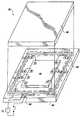
- FIG. 4is an exploded isometric view of a package with its die cover attached to its base using a heating circuit that is integral with the base in accordance with the present invention.
- FIG. 5is an exploded isometric view of a package with its die cover permanently sealed and attached to its base using a heating circuit that is integral with the base in accordance with the present invention.
- FIG. 6is a block diagram of an electronic system including the package of FIG. 4 .
- a die support member 10 of the present invention shown in FIG. 1includes a heating circuit 12 integral with a base 14 , such as a lead frame die pad 14 .
- the heating circuit 12is generally located on or near the surface of the base 14 for improved heating efficiency in a localized area of the base. Alternatively, the heating circuit 12 may be placed on the base 14 to provide a uniform heating of the entire base or predetermined portion thereof.
- any heating circuit capable of being integrated with a basewill work for purposes of this invention, including resistance-connected Metal-Oxide Semiconductor (MOS) transistors connected in series, doped resistors, epitaxial-layer resistors, pinch resistors, thin-film resistors, diffused resistors, deposited resistors, plated resistors, etched resistors, etched resistors having been etched into a substrate, polysilicon resistors, and Complimentary-MOS (CMOS) well-type resistors.
- MOSMetal-Oxide Semiconductor
- the base 14may include lead frames, either conventional or Lead-Over-Chip type, a silicon substrate having a passivated surface, a glass epoxy printed circuit board, a printed circuit board including a SIMM, DIMM, or other multi-chip modules, etc. It should be understood that the present invention is not limited to the shape and configuration of the illustrated heating circuit 12 as the heating circuit 12 can include other shapes and variations.
- the heating circuit 12attaches a bare semiconductor die 16 , such as a Dynamic Random Access Memory (DRAM) die, to the lead frame die pad 14 by heating and curing a die-attach material 18 on the surface of the lead frame die pad 14 in response to being energized by a supply voltage V S or current supply.
- a bare semiconductor die 16such as a Dynamic Random Access Memory (DRAM) die
- DRAMDynamic Random Access Memory
- the heating circuit 12can also be used to detach the bare semiconductor die 16 from the lead frame die pad 14 for purposes of reworking or replacing the bare semiconductor die 16 .
- the heating circuit 12can also be configured or shaped to provide more heat or uniform heat to predetermined parts of the die attach material and portion of the substrate or the entire substrate through variations in the shape and size of the heating circuit 12 .
- the inventive heating circuitis associated in close proximity with a single die, the heat it generates is localized and/or concentrated and/or uniform with respect to that die.
- the heating circuit of the present inventioncan attach or detach a die in the presence of neighboring electronic devices, solder joints, and adhesive joints without the excessive heating thereof.
- a die support member 20includes a heating circuit 22 integral with a base, such as a glass-epoxy printed circuit board 24 .
- a bare semiconductor die 26is attached to the printed circuit board 24 using well-known Chip-On-Board (COB) or Direct Chip-Attach (DCA) methods such as die-bond/wire-bond, Tape-Automated Bonding (TAB), or Controlled-Collapse Chip Connection (C4).
- COBChip-On-Board
- DCADirect Chip-Attach
- TABTape-Automated Bonding
- C4Controlled-Collapse Chip Connection
- the bare semiconductor die 26may include a Known-Good-Die (KGD).
- the heating circuit 22attaches a die cover 28 to the printed circuit board 24 by heating and curing an attachment material 30 on the surface of the printed circuit board 24 in response to being energized by a supply voltage VS or a current supply.
- a supply voltage VS or a current supplyA wide variety of well-known attachment materials, such as set forth hereinbefore will work for this purpose.
- the heating circuit 22can also be used to detach the die cover 28 from the printed circuit board 24 for purposes of testing, reworking or replacing the bare semiconductor die 26 .
- the heating circuit 22will work for purposes of this invention if it is incorporated into the die cover 28 rather than the printed circuit board 24 .
- the printed circuit board 24can include another heating circuit integral therewith underneath the bare semiconductor die 26 for purposes of attaching and detaching the bare semiconductor die 26 from the printed circuit board 24 .
- the heating circuit 22can be eliminated if the attachment material 30 is sufficiently conductive to act as a heating circuit itself.
- Well-known conductive attachment materialsinclude eutectic solders and metal-filled epoxy and polyamide adhesives.
- the heating circuit 22employs localized heating of the printed circuit board 24 and die cover 28 without excessive heating of other areas of the printed circuit board 24 or die cover 28 . Furthermore, the heating circuit 22 not only provides localized heat but it provides a very uniform heating of the printed circuit board 24 and/or die cover 28 . Additionally, the die cover 28 may form a hermetic seal with the printed circuit board 24 , if desired, through the use of a suitable attachment material and the heating circuit 22 .
- a die support member 20includes a heating circuit 22 integral with a base, such as a glass-epoxy printed circuit board 24 .
- a bare semiconductor die 26is attached to the leads 27 of a lead frame using adhesive tape strips 27 ′ using well-known Lead-Over-Chip (LOC) technology.
- LOCLead-Over-Chip
- the heating circuit 22attaches a die cover 28 to the printed circuit board 24 by heating and curing an attachment material 30 on the surface of the printed circuit board 24 in response to being energized by a supply voltage V S or current supply.
- V Ssupply voltage
- a wide variety of well-known attachment materials, such as set forth hereinbeforewill work for this purpose.
- the heating circuit 22can also be used to detach the die cover 28 from the printed circuit board 24 for purposes of testing, reworking or replacing the bare semiconductor die 26 . Any suitable adhesive may be used to hermetically attach the die cover 28 to the printed circuit board 24 .
- the heating circuit 22will work for purposes of this invention if it is incorporated into the die cover 28 , shown in phantom as 22 ′, rather than the printed circuit board 24 .
- the printed circuit board 24can include another heating circuit integral therewith underneath the bare semiconductor die 26 for purposes of attaching and detaching the bare semiconductor die 26 from the printed circuit board 24 .
- the heating circuit 22can be eliminated if the attachment material 30 is sufficiently conductive to act as a heating circuit itself.
- Well-known conductive attachment materialsinclude eutectic solders and metal-filled epoxy and polyamide adhesives.
- the heating circuit 22whether contained on the printed circuit board 24 and/or die cover 28 , employs localized heating of the printed circuit board 24 and die cover 28 without excessive heating of other areas of the printed circuit board 24 or die cover 28 .
- a die support membersuch as a Thin Small Outline Package (TSOP) 40 , includes a heating circuit 42 integral with a base 44 of the TSOP 40 .
- a bare semiconductor die 46is attached to a die-attach area 48 of the base 44 using well-known die-attach methods.
- the heating circuit 42attaches a die cover 50 to the base 44 by heating and curing an attachment material 52 on the surface of the base 44 in response to being energized by a supply voltage V S or current supply.
- V S or current supplyif a thermoplastic type adhesive is used, the heating circuit 42 can also be used to detach the die cover 50 from the base 44 for purposes of testing, reworking or replacing the bare semiconductor die 46 .
- Any suitable adhesivemay be used to hermetically seal the die cover 50 to the base 44 , as desired.
- the heating circuit 42merely locally, uniformly heats up the base 44 and die cover 50 for attachment and disassembly purposes.
- a die support membersuch as a Thin Small Outline Package (TSOP) 70 , includes a heating circuit 72 integral with a base 74 of the TSOP 70 extending therearound without any gap therein to be used to seal the base 74 to a die cover 80 .
- a bare semiconductor die 76is attached to a die-attach area 78 of the base 74 using well-known die-attach methods.
- the heating circuit 72attaches and seals a die cover 80 to the base 74 by heating and curing an attachment material 82 on the surface of the base 74 in response to being energized by a supply voltage V S or current supply.
- the heating circuit 72can also be used to detach the die cover 80 from the base 74 for purposes of testing, reworking or replacing the bare semiconductor die 76 . Suitable adhesives may be used to hermetically seal the die cover 80 to the base 74 . Again, the heating circuit 72 merely locally heats up the base 74 and die cover 80 for attachment and disassembly purposes.
- the TSOP 40 of FIG. 4can be incorporated into a memory device 60 of an electronic system 62 , such as a computer system, that includes an input device 64 and an output device 66 coupled to a processor 68 .
- a memory device 60 of an electronic system 62such as a computer system
- any suitable type TSOP 40can alternatively be incorporated into the input device 64 , the output device 66 , or the processor 68 .
- the processor 68or any desired type semiconductor device, may be packaged as described hereinbefore using such configurations as described hereinbefore or the like.
- the previously described inventionprovides a convenient device and method for die-attach, and for attaching a die cover, without the need for a cumbersome cure oven.
- the inventionalso provides a previously unavailable method for detaching a die or die cover for testing, reworking or replacing a die.
- the shape of the heating element of the present inventionmay be of any desired shape having any desired end connection arrangement to facilitate the desired sealing arrangement to form a hermetically sealed semiconductor die, if so desired.
- Any desired number of heating circuitsmay be used to heat localized areas of a substrate, semiconductor die, or die cover to facilitate attachment and disassembly for any desired purpose. Therefore, the invention is limited only by the appended claims, which include within their scope all equivalent devices or methods which operate according to the principles of the invention as described.
Landscapes
- Engineering & Computer Science (AREA)
- Computer Hardware Design (AREA)
- Microelectronics & Electronic Packaging (AREA)
- Power Engineering (AREA)
- Physics & Mathematics (AREA)
- Condensed Matter Physics & Semiconductors (AREA)
- General Physics & Mathematics (AREA)
- Manufacturing & Machinery (AREA)
- Geometry (AREA)
- Die Bonding (AREA)
Abstract
Description
Claims (16)
Priority Applications (1)
| Application Number | Priority Date | Filing Date | Title |
|---|---|---|---|
| US10/205,826US6696669B2 (en) | 1996-09-10 | 2002-07-25 | Circuit and method for heating an adhesive to package or rework a semiconductor die |
Applications Claiming Priority (5)
| Application Number | Priority Date | Filing Date | Title |
|---|---|---|---|
| US08/711,201US5938956A (en) | 1996-09-10 | 1996-09-10 | Circuit and method for heating an adhesive to package or rework a semiconductor die |
| US09/338,242US6111220A (en) | 1996-09-10 | 1999-06-22 | Circuit and method for heating an adhesive to package or rework a semiconductor die |
| US09/620,182US6339210B1 (en) | 1996-09-10 | 2000-07-20 | Circuit and method for heating an adhesive to package or rework a semiconductor die |
| US09/942,221US6426484B1 (en) | 1996-09-10 | 2001-08-29 | Circuit and method for heating an adhesive to package or rework a semiconductor die |
| US10/205,826US6696669B2 (en) | 1996-09-10 | 2002-07-25 | Circuit and method for heating an adhesive to package or rework a semiconductor die |
Related Parent Applications (1)
| Application Number | Title | Priority Date | Filing Date |
|---|---|---|---|
| US09/942,221ContinuationUS6426484B1 (en) | 1996-09-10 | 2001-08-29 | Circuit and method for heating an adhesive to package or rework a semiconductor die |
Publications (2)
| Publication Number | Publication Date |
|---|---|
| US20020175153A1 US20020175153A1 (en) | 2002-11-28 |
| US6696669B2true US6696669B2 (en) | 2004-02-24 |
Family
ID=27407256
Family Applications (2)
| Application Number | Title | Priority Date | Filing Date |
|---|---|---|---|
| US09/942,221Expired - LifetimeUS6426484B1 (en) | 1996-09-10 | 2001-08-29 | Circuit and method for heating an adhesive to package or rework a semiconductor die |
| US10/205,826Expired - LifetimeUS6696669B2 (en) | 1996-09-10 | 2002-07-25 | Circuit and method for heating an adhesive to package or rework a semiconductor die |
Family Applications Before (1)
| Application Number | Title | Priority Date | Filing Date |
|---|---|---|---|
| US09/942,221Expired - LifetimeUS6426484B1 (en) | 1996-09-10 | 2001-08-29 | Circuit and method for heating an adhesive to package or rework a semiconductor die |
Country Status (1)
| Country | Link |
|---|---|
| US (2) | US6426484B1 (en) |
Cited By (92)
| Publication number | Priority date | Publication date | Assignee | Title |
|---|---|---|---|---|
| US20030156397A1 (en)* | 2000-04-28 | 2003-08-21 | Reinhold Preissl | Cover device for lines in vehicles |
| US20040035840A1 (en)* | 2002-08-23 | 2004-02-26 | Michel Koopmans | Component installation, removal, and replacement apparatus and method |
| US20040238600A1 (en)* | 2003-05-22 | 2004-12-02 | Terry Tarn | Novel packaging method for microstructure and semiconductor devices |
| US20070199689A1 (en)* | 2002-01-24 | 2007-08-30 | Department Of The Navy | Lightweight thermal heat transfer apparatus |
| US20090223937A1 (en)* | 2008-03-10 | 2009-09-10 | Micron Technology, Inc. | Apparatus and methods for forming wire bonds |
| US8507363B2 (en) | 2011-06-15 | 2013-08-13 | Applied Materials, Inc. | Laser and plasma etch wafer dicing using water-soluble die attach film |
| US8557682B2 (en) | 2011-06-15 | 2013-10-15 | Applied Materials, Inc. | Multi-layer mask for substrate dicing by laser and plasma etch |
| US8557683B2 (en) | 2011-06-15 | 2013-10-15 | Applied Materials, Inc. | Multi-step and asymmetrically shaped laser beam scribing |
| US8598016B2 (en) | 2011-06-15 | 2013-12-03 | Applied Materials, Inc. | In-situ deposited mask layer for device singulation by laser scribing and plasma etch |
| US8642448B2 (en) | 2010-06-22 | 2014-02-04 | Applied Materials, Inc. | Wafer dicing using femtosecond-based laser and plasma etch |
| US8652940B2 (en) | 2012-04-10 | 2014-02-18 | Applied Materials, Inc. | Wafer dicing used hybrid multi-step laser scribing process with plasma etch |
| US8703581B2 (en) | 2011-06-15 | 2014-04-22 | Applied Materials, Inc. | Water soluble mask for substrate dicing by laser and plasma etch |
| US8759197B2 (en) | 2011-06-15 | 2014-06-24 | Applied Materials, Inc. | Multi-step and asymmetrically shaped laser beam scribing |
| US8845854B2 (en) | 2012-07-13 | 2014-09-30 | Applied Materials, Inc. | Laser, plasma etch, and backside grind process for wafer dicing |
| US8859397B2 (en) | 2012-07-13 | 2014-10-14 | Applied Materials, Inc. | Method of coating water soluble mask for laser scribing and plasma etch |
| US8883614B1 (en) | 2013-05-22 | 2014-11-11 | Applied Materials, Inc. | Wafer dicing with wide kerf by laser scribing and plasma etching hybrid approach |
| US8883615B1 (en) | 2014-03-07 | 2014-11-11 | Applied Materials, Inc. | Approaches for cleaning a wafer during hybrid laser scribing and plasma etching wafer dicing processes |
| US8912075B1 (en) | 2014-04-29 | 2014-12-16 | Applied Materials, Inc. | Wafer edge warp supression for thin wafer supported by tape frame |
| US8912078B1 (en) | 2014-04-16 | 2014-12-16 | Applied Materials, Inc. | Dicing wafers having solder bumps on wafer backside |
| US8912077B2 (en) | 2011-06-15 | 2014-12-16 | Applied Materials, Inc. | Hybrid laser and plasma etch wafer dicing using substrate carrier |
| US8927393B1 (en) | 2014-01-29 | 2015-01-06 | Applied Materials, Inc. | Water soluble mask formation by dry film vacuum lamination for laser and plasma dicing |
| US8932939B1 (en) | 2014-04-14 | 2015-01-13 | Applied Materials, Inc. | Water soluble mask formation by dry film lamination |
| US8940619B2 (en) | 2012-07-13 | 2015-01-27 | Applied Materials, Inc. | Method of diced wafer transportation |
| US8946057B2 (en) | 2012-04-24 | 2015-02-03 | Applied Materials, Inc. | Laser and plasma etch wafer dicing using UV-curable adhesive film |
| US8951819B2 (en) | 2011-07-11 | 2015-02-10 | Applied Materials, Inc. | Wafer dicing using hybrid split-beam laser scribing process with plasma etch |
| US8969177B2 (en) | 2012-06-29 | 2015-03-03 | Applied Materials, Inc. | Laser and plasma etch wafer dicing with a double sided UV-curable adhesive film |
| US8975162B2 (en) | 2012-12-20 | 2015-03-10 | Applied Materials, Inc. | Wafer dicing from wafer backside |
| US8975163B1 (en) | 2014-04-10 | 2015-03-10 | Applied Materials, Inc. | Laser-dominated laser scribing and plasma etch hybrid wafer dicing |
| US8980727B1 (en) | 2014-05-07 | 2015-03-17 | Applied Materials, Inc. | Substrate patterning using hybrid laser scribing and plasma etching processing schemes |
| US8980726B2 (en) | 2013-01-25 | 2015-03-17 | Applied Materials, Inc. | Substrate dicing by laser ablation and plasma etch damage removal for ultra-thin wafers |
| US8991329B1 (en) | 2014-01-31 | 2015-03-31 | Applied Materials, Inc. | Wafer coating |
| US8993414B2 (en) | 2012-07-13 | 2015-03-31 | Applied Materials, Inc. | Laser scribing and plasma etch for high die break strength and clean sidewall |
| US8999816B1 (en) | 2014-04-18 | 2015-04-07 | Applied Materials, Inc. | Pre-patterned dry laminate mask for wafer dicing processes |
| US9012305B1 (en) | 2014-01-29 | 2015-04-21 | Applied Materials, Inc. | Wafer dicing using hybrid laser scribing and plasma etch approach with intermediate non-reactive post mask-opening clean |
| US9018079B1 (en) | 2014-01-29 | 2015-04-28 | Applied Materials, Inc. | Wafer dicing using hybrid laser scribing and plasma etch approach with intermediate reactive post mask-opening clean |
| US9029242B2 (en) | 2011-06-15 | 2015-05-12 | Applied Materials, Inc. | Damage isolation by shaped beam delivery in laser scribing process |
| US9034771B1 (en) | 2014-05-23 | 2015-05-19 | Applied Materials, Inc. | Cooling pedestal for dicing tape thermal management during plasma dicing |
| US9041198B2 (en) | 2013-10-22 | 2015-05-26 | Applied Materials, Inc. | Maskless hybrid laser scribing and plasma etching wafer dicing process |
| US9048309B2 (en) | 2012-07-10 | 2015-06-02 | Applied Materials, Inc. | Uniform masking for wafer dicing using laser and plasma etch |
| US9076860B1 (en) | 2014-04-04 | 2015-07-07 | Applied Materials, Inc. | Residue removal from singulated die sidewall |
| US9093518B1 (en) | 2014-06-30 | 2015-07-28 | Applied Materials, Inc. | Singulation of wafers having wafer-level underfill |
| US9105710B2 (en) | 2013-08-30 | 2015-08-11 | Applied Materials, Inc. | Wafer dicing method for improving die packaging quality |
| US9112050B1 (en) | 2014-05-13 | 2015-08-18 | Applied Materials, Inc. | Dicing tape thermal management by wafer frame support ring cooling during plasma dicing |
| US9117868B1 (en) | 2014-08-12 | 2015-08-25 | Applied Materials, Inc. | Bipolar electrostatic chuck for dicing tape thermal management during plasma dicing |
| US9126285B2 (en) | 2011-06-15 | 2015-09-08 | Applied Materials, Inc. | Laser and plasma etch wafer dicing using physically-removable mask |
| US9129904B2 (en) | 2011-06-15 | 2015-09-08 | Applied Materials, Inc. | Wafer dicing using pulse train laser with multiple-pulse bursts and plasma etch |
| US9130056B1 (en) | 2014-10-03 | 2015-09-08 | Applied Materials, Inc. | Bi-layer wafer-level underfill mask for wafer dicing and approaches for performing wafer dicing |
| US9130057B1 (en) | 2014-06-30 | 2015-09-08 | Applied Materials, Inc. | Hybrid dicing process using a blade and laser |
| US9130030B1 (en) | 2014-03-07 | 2015-09-08 | Applied Materials, Inc. | Baking tool for improved wafer coating process |
| US9142459B1 (en) | 2014-06-30 | 2015-09-22 | Applied Materials, Inc. | Wafer dicing using hybrid laser scribing and plasma etch approach with mask application by vacuum lamination |
| US9159621B1 (en) | 2014-04-29 | 2015-10-13 | Applied Materials, Inc. | Dicing tape protection for wafer dicing using laser scribe process |
| US9159624B1 (en) | 2015-01-05 | 2015-10-13 | Applied Materials, Inc. | Vacuum lamination of polymeric dry films for wafer dicing using hybrid laser scribing and plasma etch approach |
| US9159574B2 (en) | 2012-08-27 | 2015-10-13 | Applied Materials, Inc. | Method of silicon etch for trench sidewall smoothing |
| US9165812B2 (en) | 2014-01-31 | 2015-10-20 | Applied Materials, Inc. | Cooled tape frame lift and low contact shadow ring for plasma heat isolation |
| US9165832B1 (en) | 2014-06-30 | 2015-10-20 | Applied Materials, Inc. | Method of die singulation using laser ablation and induction of internal defects with a laser |
| US9177861B1 (en) | 2014-09-19 | 2015-11-03 | Applied Materials, Inc. | Hybrid wafer dicing approach using laser scribing process based on an elliptical laser beam profile or a spatio-temporal controlled laser beam profile |
| US9196498B1 (en) | 2014-08-12 | 2015-11-24 | Applied Materials, Inc. | Stationary actively-cooled shadow ring for heat dissipation in plasma chamber |
| US9196536B1 (en) | 2014-09-25 | 2015-11-24 | Applied Materials, Inc. | Hybrid wafer dicing approach using a phase modulated laser beam profile laser scribing process and plasma etch process |
| US9224650B2 (en) | 2013-09-19 | 2015-12-29 | Applied Materials, Inc. | Wafer dicing from wafer backside and front side |
| US9236305B2 (en) | 2013-01-25 | 2016-01-12 | Applied Materials, Inc. | Wafer dicing with etch chamber shield ring for film frame wafer applications |
| US9245803B1 (en) | 2014-10-17 | 2016-01-26 | Applied Materials, Inc. | Hybrid wafer dicing approach using a bessel beam shaper laser scribing process and plasma etch process |
| US9252057B2 (en) | 2012-10-17 | 2016-02-02 | Applied Materials, Inc. | Laser and plasma etch wafer dicing with partial pre-curing of UV release dicing tape for film frame wafer application |
| US9275902B2 (en) | 2014-03-26 | 2016-03-01 | Applied Materials, Inc. | Dicing processes for thin wafers with bumps on wafer backside |
| US9281244B1 (en) | 2014-09-18 | 2016-03-08 | Applied Materials, Inc. | Hybrid wafer dicing approach using an adaptive optics-controlled laser scribing process and plasma etch process |
| US9293304B2 (en) | 2013-12-17 | 2016-03-22 | Applied Materials, Inc. | Plasma thermal shield for heat dissipation in plasma chamber |
| US9299614B2 (en) | 2013-12-10 | 2016-03-29 | Applied Materials, Inc. | Method and carrier for dicing a wafer |
| US9299611B2 (en) | 2014-01-29 | 2016-03-29 | Applied Materials, Inc. | Method of wafer dicing using hybrid laser scribing and plasma etch approach with mask plasma treatment for improved mask etch resistance |
| US9312177B2 (en) | 2013-12-06 | 2016-04-12 | Applied Materials, Inc. | Screen print mask for laser scribe and plasma etch wafer dicing process |
| US9330977B1 (en) | 2015-01-05 | 2016-05-03 | Applied Materials, Inc. | Hybrid wafer dicing approach using a galvo scanner and linear stage hybrid motion laser scribing process and plasma etch process |
| US9349648B2 (en) | 2014-07-22 | 2016-05-24 | Applied Materials, Inc. | Hybrid wafer dicing approach using a rectangular shaped two-dimensional top hat laser beam profile or a linear shaped one-dimensional top hat laser beam profile laser scribing process and plasma etch process |
| US9355907B1 (en) | 2015-01-05 | 2016-05-31 | Applied Materials, Inc. | Hybrid wafer dicing approach using a line shaped laser beam profile laser scribing process and plasma etch process |
| US9460966B2 (en) | 2013-10-10 | 2016-10-04 | Applied Materials, Inc. | Method and apparatus for dicing wafers having thick passivation polymer layer |
| US9478455B1 (en) | 2015-06-12 | 2016-10-25 | Applied Materials, Inc. | Thermal pyrolytic graphite shadow ring assembly for heat dissipation in plasma chamber |
| US9601375B2 (en) | 2015-04-27 | 2017-03-21 | Applied Materials, Inc. | UV-cure pre-treatment of carrier film for wafer dicing using hybrid laser scribing and plasma etch approach |
| US9620379B2 (en) | 2013-03-14 | 2017-04-11 | Applied Materials, Inc. | Multi-layer mask including non-photodefinable laser energy absorbing layer for substrate dicing by laser and plasma etch |
| US9721839B2 (en) | 2015-06-12 | 2017-08-01 | Applied Materials, Inc. | Etch-resistant water soluble mask for hybrid wafer dicing using laser scribing and plasma etch |
| US9793132B1 (en) | 2016-05-13 | 2017-10-17 | Applied Materials, Inc. | Etch mask for hybrid laser scribing and plasma etch wafer singulation process |
| US9852997B2 (en) | 2016-03-25 | 2017-12-26 | Applied Materials, Inc. | Hybrid wafer dicing approach using a rotating beam laser scribing process and plasma etch process |
| US9972575B2 (en) | 2016-03-03 | 2018-05-15 | Applied Materials, Inc. | Hybrid wafer dicing approach using a split beam laser scribing process and plasma etch process |
| US20180185964A1 (en)* | 2015-11-09 | 2018-07-05 | Furukawa Electric Co., Ltd. | Method of producing semiconductor chip, and mask-integrated surface protective tape used therein |
| US10363629B2 (en) | 2017-06-01 | 2019-07-30 | Applied Materials, Inc. | Mitigation of particle contamination for wafer dicing processes |
| US10535561B2 (en) | 2018-03-12 | 2020-01-14 | Applied Materials, Inc. | Hybrid wafer dicing approach using a multiple pass laser scribing process and plasma etch process |
| US10576912B2 (en)* | 2015-12-16 | 2020-03-03 | Autonetworks Technologies, Ltd. | Circuit assembly and electrical junction box |
| US10692765B2 (en) | 2014-11-07 | 2020-06-23 | Applied Materials, Inc. | Transfer arm for film frame substrate handling during plasma singulation of wafers |
| US10903121B1 (en) | 2019-08-14 | 2021-01-26 | Applied Materials, Inc. | Hybrid wafer dicing approach using a uniform rotating beam laser scribing process and plasma etch process |
| US11011424B2 (en) | 2019-08-06 | 2021-05-18 | Applied Materials, Inc. | Hybrid wafer dicing approach using a spatially multi-focused laser beam laser scribing process and plasma etch process |
| US11158540B2 (en) | 2017-05-26 | 2021-10-26 | Applied Materials, Inc. | Light-absorbing mask for hybrid laser scribing and plasma etch wafer singulation process |
| US11195756B2 (en) | 2014-09-19 | 2021-12-07 | Applied Materials, Inc. | Proximity contact cover ring for plasma dicing |
| US11211247B2 (en) | 2020-01-30 | 2021-12-28 | Applied Materials, Inc. | Water soluble organic-inorganic hybrid mask formulations and their applications |
| US11342226B2 (en) | 2019-08-13 | 2022-05-24 | Applied Materials, Inc. | Hybrid wafer dicing approach using an actively-focused laser beam laser scribing process and plasma etch process |
| US11355394B2 (en) | 2018-09-13 | 2022-06-07 | Applied Materials, Inc. | Wafer dicing using hybrid laser scribing and plasma etch approach with intermediate breakthrough treatment |
| US11600492B2 (en) | 2019-12-10 | 2023-03-07 | Applied Materials, Inc. | Electrostatic chuck with reduced current leakage for hybrid laser scribing and plasma etch wafer singulation process |
Families Citing this family (20)
| Publication number | Priority date | Publication date | Assignee | Title |
|---|---|---|---|---|
| US6426484B1 (en)* | 1996-09-10 | 2002-07-30 | Micron Technology, Inc. | Circuit and method for heating an adhesive to package or rework a semiconductor die |
| US6574858B1 (en)* | 1998-02-13 | 2003-06-10 | Micron Technology, Inc. | Method of manufacturing a chip package |
| US6853067B1 (en) | 1999-10-12 | 2005-02-08 | Microassembly Technologies, Inc. | Microelectromechanical systems using thermocompression bonding |
| US20020096421A1 (en)* | 2000-11-29 | 2002-07-25 | Cohn Michael B. | MEMS device with integral packaging |
| US6667461B1 (en)* | 2002-06-19 | 2003-12-23 | Tyco Electronics Corporation | Multiple load protection and control device |
| US7170155B2 (en)* | 2003-06-25 | 2007-01-30 | Intel Corporation | MEMS RF switch module including a vertical via |
| USD502151S1 (en)* | 2003-09-02 | 2005-02-22 | International Rectifier Corporation | Semiconductor package |
| US20060284556A1 (en)* | 2003-11-12 | 2006-12-21 | Tremel James D | Electronic devices and a method for encapsulating electronic devices |
| US20060283546A1 (en)* | 2003-11-12 | 2006-12-21 | Tremel James D | Method for encapsulating electronic devices and a sealing assembly for the electronic devices |
| JP4980718B2 (en)* | 2003-11-12 | 2012-07-18 | イー・アイ・デュポン・ドウ・ヌムール・アンド・カンパニー | Encapsulation assembly for electronic devices |
| US20050238803A1 (en)* | 2003-11-12 | 2005-10-27 | Tremel James D | Method for adhering getter material to a surface for use in electronic devices |
| US7692521B1 (en) | 2005-05-12 | 2010-04-06 | Microassembly Technologies, Inc. | High force MEMS device |
| US8173995B2 (en) | 2005-12-23 | 2012-05-08 | E. I. Du Pont De Nemours And Company | Electronic device including an organic active layer and process for forming the electronic device |
| US9125301B2 (en)* | 2011-10-18 | 2015-09-01 | Integrated Microwave Corporation | Integral heater assembly and method for carrier or host board of electronic package assembly |
| CN103682177B (en)* | 2013-12-16 | 2015-03-25 | 深圳市华星光电技术有限公司 | Manufacturing method of flexible OLED panel |
| US20160181574A1 (en)* | 2014-01-03 | 2016-06-23 | Shenzhen China Star Optoelectronics Technology Co., Ltd. | Method for manufacturing flexible oled (organic light emitting diode) panel |
| US20170179066A1 (en)* | 2015-12-18 | 2017-06-22 | Russell S. Aoki | Bulk solder removal on processor packaging |
| US10688731B2 (en) | 2018-01-30 | 2020-06-23 | Te Connectivity Corporation | System and method for bonding structural components |
| US11534086B2 (en) | 2020-10-30 | 2022-12-27 | Medtronic Minimed, Inc. | Low-profile wearable medical device |
| CN118039578B (en)* | 2024-04-12 | 2024-06-11 | 深圳市元视芯智能科技有限公司 | Image sensor and image sensor system |
Citations (24)
| Publication number | Priority date | Publication date | Assignee | Title |
|---|---|---|---|---|
| US4256945A (en) | 1979-08-31 | 1981-03-17 | Iris Associates | Alternating current electrically resistive heating element having intrinsic temperature control |
| US4448306A (en) | 1981-02-09 | 1984-05-15 | British Telecommunications | Integrated circuit chip carrier |
| US4623401A (en) | 1984-03-06 | 1986-11-18 | Metcal, Inc. | Heat treatment with an autoregulating heater |
| US4695713A (en) | 1982-09-30 | 1987-09-22 | Metcal, Inc. | Autoregulating, electrically shielded heater |
| US4701587A (en) | 1979-08-31 | 1987-10-20 | Metcal, Inc. | Shielded heating element having intrinsic temperature control |
| US4717814A (en) | 1983-06-27 | 1988-01-05 | Metcal, Inc. | Slotted autoregulating heater |
| US4745264A (en) | 1984-03-06 | 1988-05-17 | Metcal, Inc. | High efficiency autoregulating heater |
| US4769525A (en) | 1986-09-02 | 1988-09-06 | Hughes Aircraft Company | Circuit package attachment apparatus and method |
| US4792683A (en) | 1987-01-16 | 1988-12-20 | Hughes Aircraft Company | Thermal technique for simultaneous testing of circuit board solder joints |
| US5010233A (en) | 1988-11-29 | 1991-04-23 | Amp Incorporated | Self regulating temperature heater as an integral part of a printed circuit board |
| US5117279A (en) | 1990-03-23 | 1992-05-26 | Motorola, Inc. | Semiconductor device having a low temperature uv-cured epoxy seal |
| US5175409A (en) | 1985-06-20 | 1992-12-29 | Metcal, Inc. | Self-soldering flexible circuit connector |
| US5194695A (en) | 1990-11-02 | 1993-03-16 | Ak Technology, Inc. | Thermoplastic semiconductor package |
| US5239806A (en) | 1990-11-02 | 1993-08-31 | Ak Technology, Inc. | Thermoplastic semiconductor package and method of producing it |
| US5418189A (en) | 1990-09-24 | 1995-05-23 | Texas Instruments Incorporated | Integrated circuit device and method to prevent cracking during surface mount |
| US5498899A (en) | 1992-05-28 | 1996-03-12 | Co.Ri.M.Me. | Spiral resistor integrated on a semiconductor substrate |
| US5500555A (en) | 1994-04-11 | 1996-03-19 | Lsi Logic Corporation | Multi-layer semiconductor package substrate with thermally-conductive prepeg layer |
| US5521426A (en) | 1992-09-09 | 1996-05-28 | Texas Instruments Incorporated | Reduced capacitance lead frame for lead on chip package |
| US5596171A (en)* | 1993-05-21 | 1997-01-21 | Harris; James M. | Package for a high frequency semiconductor device and methods for fabricating and connecting the same to an external circuit |
| US5598031A (en) | 1993-06-23 | 1997-01-28 | Vlsi Technology, Inc. | Electrically and thermally enhanced package using a separate silicon substrate |
| US5673845A (en)* | 1996-06-17 | 1997-10-07 | Micron Technology, Inc. | Lead penetrating clamping system |
| US5840599A (en)* | 1989-06-30 | 1998-11-24 | Texas Instruments Incorporated | Process of packaging an integrated circuit with a conductive material between a lead frame and the face of the circuit |
| US5938956A (en)* | 1996-09-10 | 1999-08-17 | Micron Technology, Inc. | Circuit and method for heating an adhesive to package or rework a semiconductor die |
| US6426484B1 (en)* | 1996-09-10 | 2002-07-30 | Micron Technology, Inc. | Circuit and method for heating an adhesive to package or rework a semiconductor die |
- 2001
- 2001-08-29USUS09/942,221patent/US6426484B1/ennot_activeExpired - Lifetime
- 2002
- 2002-07-25USUS10/205,826patent/US6696669B2/ennot_activeExpired - Lifetime
Patent Citations (26)
| Publication number | Priority date | Publication date | Assignee | Title |
|---|---|---|---|---|
| US4256945A (en) | 1979-08-31 | 1981-03-17 | Iris Associates | Alternating current electrically resistive heating element having intrinsic temperature control |
| US4701587A (en) | 1979-08-31 | 1987-10-20 | Metcal, Inc. | Shielded heating element having intrinsic temperature control |
| US4448306A (en) | 1981-02-09 | 1984-05-15 | British Telecommunications | Integrated circuit chip carrier |
| US4695713A (en) | 1982-09-30 | 1987-09-22 | Metcal, Inc. | Autoregulating, electrically shielded heater |
| US4717814A (en) | 1983-06-27 | 1988-01-05 | Metcal, Inc. | Slotted autoregulating heater |
| US4745264A (en) | 1984-03-06 | 1988-05-17 | Metcal, Inc. | High efficiency autoregulating heater |
| US4623401A (en) | 1984-03-06 | 1986-11-18 | Metcal, Inc. | Heat treatment with an autoregulating heater |
| US5175409A (en) | 1985-06-20 | 1992-12-29 | Metcal, Inc. | Self-soldering flexible circuit connector |
| US4769525A (en) | 1986-09-02 | 1988-09-06 | Hughes Aircraft Company | Circuit package attachment apparatus and method |
| US4792683A (en) | 1987-01-16 | 1988-12-20 | Hughes Aircraft Company | Thermal technique for simultaneous testing of circuit board solder joints |
| US5010233A (en) | 1988-11-29 | 1991-04-23 | Amp Incorporated | Self regulating temperature heater as an integral part of a printed circuit board |
| US5840599A (en)* | 1989-06-30 | 1998-11-24 | Texas Instruments Incorporated | Process of packaging an integrated circuit with a conductive material between a lead frame and the face of the circuit |
| US5117279A (en) | 1990-03-23 | 1992-05-26 | Motorola, Inc. | Semiconductor device having a low temperature uv-cured epoxy seal |
| US5418189A (en) | 1990-09-24 | 1995-05-23 | Texas Instruments Incorporated | Integrated circuit device and method to prevent cracking during surface mount |
| US5194695A (en) | 1990-11-02 | 1993-03-16 | Ak Technology, Inc. | Thermoplastic semiconductor package |
| US5239806A (en) | 1990-11-02 | 1993-08-31 | Ak Technology, Inc. | Thermoplastic semiconductor package and method of producing it |
| US5498899A (en) | 1992-05-28 | 1996-03-12 | Co.Ri.M.Me. | Spiral resistor integrated on a semiconductor substrate |
| US5521426A (en) | 1992-09-09 | 1996-05-28 | Texas Instruments Incorporated | Reduced capacitance lead frame for lead on chip package |
| US5596171A (en)* | 1993-05-21 | 1997-01-21 | Harris; James M. | Package for a high frequency semiconductor device and methods for fabricating and connecting the same to an external circuit |
| US5598031A (en) | 1993-06-23 | 1997-01-28 | Vlsi Technology, Inc. | Electrically and thermally enhanced package using a separate silicon substrate |
| US5500555A (en) | 1994-04-11 | 1996-03-19 | Lsi Logic Corporation | Multi-layer semiconductor package substrate with thermally-conductive prepeg layer |
| US5673845A (en)* | 1996-06-17 | 1997-10-07 | Micron Technology, Inc. | Lead penetrating clamping system |
| US5938956A (en)* | 1996-09-10 | 1999-08-17 | Micron Technology, Inc. | Circuit and method for heating an adhesive to package or rework a semiconductor die |
| US6111220A (en)* | 1996-09-10 | 2000-08-29 | Micron Technology, Inc. | Circuit and method for heating an adhesive to package or rework a semiconductor die |
| US6339210B1 (en)* | 1996-09-10 | 2002-01-15 | Micron Technology, Inc. | Circuit and method for heating an adhesive to package or rework a semiconductor die |
| US6426484B1 (en)* | 1996-09-10 | 2002-07-30 | Micron Technology, Inc. | Circuit and method for heating an adhesive to package or rework a semiconductor die |
Cited By (126)
| Publication number | Priority date | Publication date | Assignee | Title |
|---|---|---|---|---|
| US20030156397A1 (en)* | 2000-04-28 | 2003-08-21 | Reinhold Preissl | Cover device for lines in vehicles |
| US7030322B2 (en)* | 2000-04-28 | 2006-04-18 | Robert Bosch Gmbh | Cover device for lines in vehicles |
| US20070199689A1 (en)* | 2002-01-24 | 2007-08-30 | Department Of The Navy | Lightweight thermal heat transfer apparatus |
| US7284600B2 (en)* | 2002-01-24 | 2007-10-23 | United States Of America As Represented By The Secretary Of The Navy | Process of making a lightweight thermal heat transfer apparatus |
| US20040035840A1 (en)* | 2002-08-23 | 2004-02-26 | Michel Koopmans | Component installation, removal, and replacement apparatus and method |
| US6911624B2 (en)* | 2002-08-23 | 2005-06-28 | Micron Technology, Inc. | Component installation, removal, and replacement apparatus and method |
| US20090072380A1 (en)* | 2003-05-22 | 2009-03-19 | Texas Instruments Incorporated | Microelectromechanical Device Packages with Integral Heaters |
| US20040238600A1 (en)* | 2003-05-22 | 2004-12-02 | Terry Tarn | Novel packaging method for microstructure and semiconductor devices |
| US7402878B2 (en)* | 2003-05-22 | 2008-07-22 | Texas Instruments Incorporated | Packaging method for microstructure and semiconductor devices |
| US7449773B2 (en)* | 2003-05-22 | 2008-11-11 | Texas Instruments Incorporated | Microelectromechanical device packages with integral heaters |
| US20050185248A1 (en)* | 2003-05-22 | 2005-08-25 | Terry Tarn | Microelectromechanical device packages with integral heaters |
| US7872338B2 (en)* | 2003-05-22 | 2011-01-18 | Texas Instruments Incorporated | Microelectromechanical device packages with integral heaters |
| US20090223937A1 (en)* | 2008-03-10 | 2009-09-10 | Micron Technology, Inc. | Apparatus and methods for forming wire bonds |
| US8444044B2 (en) | 2008-03-10 | 2013-05-21 | Micron Technology, Inc. | Apparatus and methods for forming wire bonds |
| US9245802B2 (en) | 2010-06-22 | 2016-01-26 | Applied Materials, Inc. | Wafer dicing using femtosecond-based laser and plasma etch |
| US8853056B2 (en) | 2010-06-22 | 2014-10-07 | Applied Materials, Inc. | Wafer dicing using femtosecond-based laser and plasma etch |
| US10163713B2 (en) | 2010-06-22 | 2018-12-25 | Applied Materials, Inc. | Wafer dicing using femtosecond-based laser and plasma etch |
| US10566238B2 (en) | 2010-06-22 | 2020-02-18 | Applied Materials, Inc. | Wafer dicing using femtosecond-based laser and plasma etch |
| US8642448B2 (en) | 2010-06-22 | 2014-02-04 | Applied Materials, Inc. | Wafer dicing using femtosecond-based laser and plasma etch |
| US10714390B2 (en) | 2010-06-22 | 2020-07-14 | Applied Materials, Inc. | Wafer dicing using femtosecond-based laser and plasma etch |
| US10910271B2 (en) | 2010-06-22 | 2021-02-02 | Applied Materials, Inc. | Wafer dicing using femtosecond-based laser and plasma etch |
| US11621194B2 (en) | 2010-06-22 | 2023-04-04 | Applied Materials, Inc. | Wafer dicing using femtosecond-based laser and plasma etch |
| US12131952B2 (en) | 2010-06-22 | 2024-10-29 | Applied Materials, Inc. | Wafer dicing using femtosecond-based laser and plasma etch |
| US9126285B2 (en) | 2011-06-15 | 2015-09-08 | Applied Materials, Inc. | Laser and plasma etch wafer dicing using physically-removable mask |
| US8703581B2 (en) | 2011-06-15 | 2014-04-22 | Applied Materials, Inc. | Water soluble mask for substrate dicing by laser and plasma etch |
| US9054176B2 (en) | 2011-06-15 | 2015-06-09 | Applied Materials, Inc. | Multi-step and asymmetrically shaped laser beam scribing |
| US9224625B2 (en) | 2011-06-15 | 2015-12-29 | Applied Materials, Inc. | Laser and plasma etch wafer dicing using water-soluble die attach film |
| US9218992B2 (en) | 2011-06-15 | 2015-12-22 | Applied Materials, Inc. | Hybrid laser and plasma etch wafer dicing using substrate carrier |
| US8557682B2 (en) | 2011-06-15 | 2013-10-15 | Applied Materials, Inc. | Multi-layer mask for substrate dicing by laser and plasma etch |
| US8759197B2 (en) | 2011-06-15 | 2014-06-24 | Applied Materials, Inc. | Multi-step and asymmetrically shaped laser beam scribing |
| US8912077B2 (en) | 2011-06-15 | 2014-12-16 | Applied Materials, Inc. | Hybrid laser and plasma etch wafer dicing using substrate carrier |
| US8557683B2 (en) | 2011-06-15 | 2013-10-15 | Applied Materials, Inc. | Multi-step and asymmetrically shaped laser beam scribing |
| US8598016B2 (en) | 2011-06-15 | 2013-12-03 | Applied Materials, Inc. | In-situ deposited mask layer for device singulation by laser scribing and plasma etch |
| US9029242B2 (en) | 2011-06-15 | 2015-05-12 | Applied Materials, Inc. | Damage isolation by shaped beam delivery in laser scribing process |
| US8507363B2 (en) | 2011-06-15 | 2013-08-13 | Applied Materials, Inc. | Laser and plasma etch wafer dicing using water-soluble die attach film |
| US9129904B2 (en) | 2011-06-15 | 2015-09-08 | Applied Materials, Inc. | Wafer dicing using pulse train laser with multiple-pulse bursts and plasma etch |
| US10112259B2 (en) | 2011-06-15 | 2018-10-30 | Applied Materials, Inc. | Damage isolation by shaped beam delivery in laser scribing process |
| US9263308B2 (en) | 2011-06-15 | 2016-02-16 | Applied Materials, Inc. | Water soluble mask for substrate dicing by laser and plasma etch |
| US8951819B2 (en) | 2011-07-11 | 2015-02-10 | Applied Materials, Inc. | Wafer dicing using hybrid split-beam laser scribing process with plasma etch |
| US8846498B2 (en) | 2012-04-10 | 2014-09-30 | Applied Materials, Inc. | Wafer dicing using hybrid multi-step laser scribing process with plasma etch |
| US8652940B2 (en) | 2012-04-10 | 2014-02-18 | Applied Materials, Inc. | Wafer dicing used hybrid multi-step laser scribing process with plasma etch |
| US8946057B2 (en) | 2012-04-24 | 2015-02-03 | Applied Materials, Inc. | Laser and plasma etch wafer dicing using UV-curable adhesive film |
| US8969177B2 (en) | 2012-06-29 | 2015-03-03 | Applied Materials, Inc. | Laser and plasma etch wafer dicing with a double sided UV-curable adhesive film |
| US9048309B2 (en) | 2012-07-10 | 2015-06-02 | Applied Materials, Inc. | Uniform masking for wafer dicing using laser and plasma etch |
| US8993414B2 (en) | 2012-07-13 | 2015-03-31 | Applied Materials, Inc. | Laser scribing and plasma etch for high die break strength and clean sidewall |
| US9177864B2 (en) | 2012-07-13 | 2015-11-03 | Applied Materials, Inc. | Method of coating water soluble mask for laser scribing and plasma etch |
| US8940619B2 (en) | 2012-07-13 | 2015-01-27 | Applied Materials, Inc. | Method of diced wafer transportation |
| US8845854B2 (en) | 2012-07-13 | 2014-09-30 | Applied Materials, Inc. | Laser, plasma etch, and backside grind process for wafer dicing |
| US8859397B2 (en) | 2012-07-13 | 2014-10-14 | Applied Materials, Inc. | Method of coating water soluble mask for laser scribing and plasma etch |
| US9159574B2 (en) | 2012-08-27 | 2015-10-13 | Applied Materials, Inc. | Method of silicon etch for trench sidewall smoothing |
| US9252057B2 (en) | 2012-10-17 | 2016-02-02 | Applied Materials, Inc. | Laser and plasma etch wafer dicing with partial pre-curing of UV release dicing tape for film frame wafer application |
| US8975162B2 (en) | 2012-12-20 | 2015-03-10 | Applied Materials, Inc. | Wafer dicing from wafer backside |
| US9236305B2 (en) | 2013-01-25 | 2016-01-12 | Applied Materials, Inc. | Wafer dicing with etch chamber shield ring for film frame wafer applications |
| US8980726B2 (en) | 2013-01-25 | 2015-03-17 | Applied Materials, Inc. | Substrate dicing by laser ablation and plasma etch damage removal for ultra-thin wafers |
| US9620379B2 (en) | 2013-03-14 | 2017-04-11 | Applied Materials, Inc. | Multi-layer mask including non-photodefinable laser energy absorbing layer for substrate dicing by laser and plasma etch |
| US8883614B1 (en) | 2013-05-22 | 2014-11-11 | Applied Materials, Inc. | Wafer dicing with wide kerf by laser scribing and plasma etching hybrid approach |
| US9105710B2 (en) | 2013-08-30 | 2015-08-11 | Applied Materials, Inc. | Wafer dicing method for improving die packaging quality |
| US9224650B2 (en) | 2013-09-19 | 2015-12-29 | Applied Materials, Inc. | Wafer dicing from wafer backside and front side |
| US9460966B2 (en) | 2013-10-10 | 2016-10-04 | Applied Materials, Inc. | Method and apparatus for dicing wafers having thick passivation polymer layer |
| US9041198B2 (en) | 2013-10-22 | 2015-05-26 | Applied Materials, Inc. | Maskless hybrid laser scribing and plasma etching wafer dicing process |
| US9209084B2 (en) | 2013-10-22 | 2015-12-08 | Applied Materials, Inc. | Maskless hybrid laser scribing and plasma etching wafer dicing process |
| US9312177B2 (en) | 2013-12-06 | 2016-04-12 | Applied Materials, Inc. | Screen print mask for laser scribe and plasma etch wafer dicing process |
| US9299614B2 (en) | 2013-12-10 | 2016-03-29 | Applied Materials, Inc. | Method and carrier for dicing a wafer |
| US9293304B2 (en) | 2013-12-17 | 2016-03-22 | Applied Materials, Inc. | Plasma thermal shield for heat dissipation in plasma chamber |
| US8927393B1 (en) | 2014-01-29 | 2015-01-06 | Applied Materials, Inc. | Water soluble mask formation by dry film vacuum lamination for laser and plasma dicing |
| US9299611B2 (en) | 2014-01-29 | 2016-03-29 | Applied Materials, Inc. | Method of wafer dicing using hybrid laser scribing and plasma etch approach with mask plasma treatment for improved mask etch resistance |
| US9012305B1 (en) | 2014-01-29 | 2015-04-21 | Applied Materials, Inc. | Wafer dicing using hybrid laser scribing and plasma etch approach with intermediate non-reactive post mask-opening clean |
| US9018079B1 (en) | 2014-01-29 | 2015-04-28 | Applied Materials, Inc. | Wafer dicing using hybrid laser scribing and plasma etch approach with intermediate reactive post mask-opening clean |
| US9165812B2 (en) | 2014-01-31 | 2015-10-20 | Applied Materials, Inc. | Cooled tape frame lift and low contact shadow ring for plasma heat isolation |
| US8991329B1 (en) | 2014-01-31 | 2015-03-31 | Applied Materials, Inc. | Wafer coating |
| US9236284B2 (en) | 2014-01-31 | 2016-01-12 | Applied Materials, Inc. | Cooled tape frame lift and low contact shadow ring for plasma heat isolation |
| US9768014B2 (en) | 2014-01-31 | 2017-09-19 | Applied Materials, Inc. | Wafer coating |
| US9130030B1 (en) | 2014-03-07 | 2015-09-08 | Applied Materials, Inc. | Baking tool for improved wafer coating process |
| US8883615B1 (en) | 2014-03-07 | 2014-11-11 | Applied Materials, Inc. | Approaches for cleaning a wafer during hybrid laser scribing and plasma etching wafer dicing processes |
| US9275902B2 (en) | 2014-03-26 | 2016-03-01 | Applied Materials, Inc. | Dicing processes for thin wafers with bumps on wafer backside |
| US9076860B1 (en) | 2014-04-04 | 2015-07-07 | Applied Materials, Inc. | Residue removal from singulated die sidewall |
| US8975163B1 (en) | 2014-04-10 | 2015-03-10 | Applied Materials, Inc. | Laser-dominated laser scribing and plasma etch hybrid wafer dicing |
| US9583375B2 (en) | 2014-04-14 | 2017-02-28 | Applied Materials, Inc. | Water soluble mask formation by dry film lamination |
| US8932939B1 (en) | 2014-04-14 | 2015-01-13 | Applied Materials, Inc. | Water soluble mask formation by dry film lamination |
| US8912078B1 (en) | 2014-04-16 | 2014-12-16 | Applied Materials, Inc. | Dicing wafers having solder bumps on wafer backside |
| US9343366B2 (en) | 2014-04-16 | 2016-05-17 | Applied Materials, Inc. | Dicing wafers having solder bumps on wafer backside |
| US8999816B1 (en) | 2014-04-18 | 2015-04-07 | Applied Materials, Inc. | Pre-patterned dry laminate mask for wafer dicing processes |
| US8912075B1 (en) | 2014-04-29 | 2014-12-16 | Applied Materials, Inc. | Wafer edge warp supression for thin wafer supported by tape frame |
| US9269604B2 (en) | 2014-04-29 | 2016-02-23 | Applied Materials, Inc. | Wafer edge warp suppression for thin wafer supported by tape frame |
| US9159621B1 (en) | 2014-04-29 | 2015-10-13 | Applied Materials, Inc. | Dicing tape protection for wafer dicing using laser scribe process |
| US8980727B1 (en) | 2014-05-07 | 2015-03-17 | Applied Materials, Inc. | Substrate patterning using hybrid laser scribing and plasma etching processing schemes |
| US9112050B1 (en) | 2014-05-13 | 2015-08-18 | Applied Materials, Inc. | Dicing tape thermal management by wafer frame support ring cooling during plasma dicing |
| US9034771B1 (en) | 2014-05-23 | 2015-05-19 | Applied Materials, Inc. | Cooling pedestal for dicing tape thermal management during plasma dicing |
| US9165832B1 (en) | 2014-06-30 | 2015-10-20 | Applied Materials, Inc. | Method of die singulation using laser ablation and induction of internal defects with a laser |
| US9142459B1 (en) | 2014-06-30 | 2015-09-22 | Applied Materials, Inc. | Wafer dicing using hybrid laser scribing and plasma etch approach with mask application by vacuum lamination |
| US9093518B1 (en) | 2014-06-30 | 2015-07-28 | Applied Materials, Inc. | Singulation of wafers having wafer-level underfill |
| US9130057B1 (en) | 2014-06-30 | 2015-09-08 | Applied Materials, Inc. | Hybrid dicing process using a blade and laser |
| US9349648B2 (en) | 2014-07-22 | 2016-05-24 | Applied Materials, Inc. | Hybrid wafer dicing approach using a rectangular shaped two-dimensional top hat laser beam profile or a linear shaped one-dimensional top hat laser beam profile laser scribing process and plasma etch process |
| US9117868B1 (en) | 2014-08-12 | 2015-08-25 | Applied Materials, Inc. | Bipolar electrostatic chuck for dicing tape thermal management during plasma dicing |
| US9196498B1 (en) | 2014-08-12 | 2015-11-24 | Applied Materials, Inc. | Stationary actively-cooled shadow ring for heat dissipation in plasma chamber |
| US9281244B1 (en) | 2014-09-18 | 2016-03-08 | Applied Materials, Inc. | Hybrid wafer dicing approach using an adaptive optics-controlled laser scribing process and plasma etch process |
| US9177861B1 (en) | 2014-09-19 | 2015-11-03 | Applied Materials, Inc. | Hybrid wafer dicing approach using laser scribing process based on an elliptical laser beam profile or a spatio-temporal controlled laser beam profile |
| US11195756B2 (en) | 2014-09-19 | 2021-12-07 | Applied Materials, Inc. | Proximity contact cover ring for plasma dicing |
| US9196536B1 (en) | 2014-09-25 | 2015-11-24 | Applied Materials, Inc. | Hybrid wafer dicing approach using a phase modulated laser beam profile laser scribing process and plasma etch process |
| US9130056B1 (en) | 2014-10-03 | 2015-09-08 | Applied Materials, Inc. | Bi-layer wafer-level underfill mask for wafer dicing and approaches for performing wafer dicing |
| US9245803B1 (en) | 2014-10-17 | 2016-01-26 | Applied Materials, Inc. | Hybrid wafer dicing approach using a bessel beam shaper laser scribing process and plasma etch process |
| US10692765B2 (en) | 2014-11-07 | 2020-06-23 | Applied Materials, Inc. | Transfer arm for film frame substrate handling during plasma singulation of wafers |
| US9355907B1 (en) | 2015-01-05 | 2016-05-31 | Applied Materials, Inc. | Hybrid wafer dicing approach using a line shaped laser beam profile laser scribing process and plasma etch process |
| US9159624B1 (en) | 2015-01-05 | 2015-10-13 | Applied Materials, Inc. | Vacuum lamination of polymeric dry films for wafer dicing using hybrid laser scribing and plasma etch approach |
| US9330977B1 (en) | 2015-01-05 | 2016-05-03 | Applied Materials, Inc. | Hybrid wafer dicing approach using a galvo scanner and linear stage hybrid motion laser scribing process and plasma etch process |
| US9601375B2 (en) | 2015-04-27 | 2017-03-21 | Applied Materials, Inc. | UV-cure pre-treatment of carrier film for wafer dicing using hybrid laser scribing and plasma etch approach |
| US9721839B2 (en) | 2015-06-12 | 2017-08-01 | Applied Materials, Inc. | Etch-resistant water soluble mask for hybrid wafer dicing using laser scribing and plasma etch |
| US9478455B1 (en) | 2015-06-12 | 2016-10-25 | Applied Materials, Inc. | Thermal pyrolytic graphite shadow ring assembly for heat dissipation in plasma chamber |
| US10307866B2 (en)* | 2015-11-09 | 2019-06-04 | Furukawa Electric Co., Ltd. | Method of producing semiconductor chip, and mask-integrated surface protective tape used therein |
| US20180185964A1 (en)* | 2015-11-09 | 2018-07-05 | Furukawa Electric Co., Ltd. | Method of producing semiconductor chip, and mask-integrated surface protective tape used therein |
| US10576912B2 (en)* | 2015-12-16 | 2020-03-03 | Autonetworks Technologies, Ltd. | Circuit assembly and electrical junction box |
| US11217536B2 (en) | 2016-03-03 | 2022-01-04 | Applied Materials, Inc. | Hybrid wafer dicing approach using a split beam laser scribing process and plasma etch process |
| US9972575B2 (en) | 2016-03-03 | 2018-05-15 | Applied Materials, Inc. | Hybrid wafer dicing approach using a split beam laser scribing process and plasma etch process |
| US9852997B2 (en) | 2016-03-25 | 2017-12-26 | Applied Materials, Inc. | Hybrid wafer dicing approach using a rotating beam laser scribing process and plasma etch process |
| US9793132B1 (en) | 2016-05-13 | 2017-10-17 | Applied Materials, Inc. | Etch mask for hybrid laser scribing and plasma etch wafer singulation process |
| US11158540B2 (en) | 2017-05-26 | 2021-10-26 | Applied Materials, Inc. | Light-absorbing mask for hybrid laser scribing and plasma etch wafer singulation process |
| US10363629B2 (en) | 2017-06-01 | 2019-07-30 | Applied Materials, Inc. | Mitigation of particle contamination for wafer dicing processes |
| US10661383B2 (en) | 2017-06-01 | 2020-05-26 | Applied Materials, Inc. | Mitigation of particle contamination for wafer dicing processes |
| US10535561B2 (en) | 2018-03-12 | 2020-01-14 | Applied Materials, Inc. | Hybrid wafer dicing approach using a multiple pass laser scribing process and plasma etch process |
| US11355394B2 (en) | 2018-09-13 | 2022-06-07 | Applied Materials, Inc. | Wafer dicing using hybrid laser scribing and plasma etch approach with intermediate breakthrough treatment |
| US11011424B2 (en) | 2019-08-06 | 2021-05-18 | Applied Materials, Inc. | Hybrid wafer dicing approach using a spatially multi-focused laser beam laser scribing process and plasma etch process |
| US11342226B2 (en) | 2019-08-13 | 2022-05-24 | Applied Materials, Inc. | Hybrid wafer dicing approach using an actively-focused laser beam laser scribing process and plasma etch process |
| US10903121B1 (en) | 2019-08-14 | 2021-01-26 | Applied Materials, Inc. | Hybrid wafer dicing approach using a uniform rotating beam laser scribing process and plasma etch process |
| US11600492B2 (en) | 2019-12-10 | 2023-03-07 | Applied Materials, Inc. | Electrostatic chuck with reduced current leakage for hybrid laser scribing and plasma etch wafer singulation process |
| US11211247B2 (en) | 2020-01-30 | 2021-12-28 | Applied Materials, Inc. | Water soluble organic-inorganic hybrid mask formulations and their applications |
| US11764061B2 (en) | 2020-01-30 | 2023-09-19 | Applied Materials, Inc. | Water soluble organic-inorganic hybrid mask formulations and their applications |
Also Published As
| Publication number | Publication date |
|---|---|
| US6426484B1 (en) | 2002-07-30 |
| US20020175153A1 (en) | 2002-11-28 |
| US20020108940A1 (en) | 2002-08-15 |
Similar Documents
| Publication | Publication Date | Title |
|---|---|---|
| US6696669B2 (en) | Circuit and method for heating an adhesive to package or rework a semiconductor die | |
| US6339210B1 (en) | Circuit and method for heating an adhesive to package or rework a semiconductor die | |
| US6735859B2 (en) | Method of manufacturing chip scale package | |
| US6326687B1 (en) | IC package with dual heat spreaders | |
| US6122171A (en) | Heat sink chip package and method of making | |
| JPH09326452A (en) | Semiconductor package | |
| US20020173069A1 (en) | Mounting structure of semiconductor chip, semiconductor device and method of making the semiconductor device | |
| US20060186533A1 (en) | Chip scale package with heat spreader | |
| US6682954B1 (en) | Method for employing piggyback multiple die #3 | |
| JP3655338B2 (en) | Resin-sealed semiconductor device and manufacturing method thereof | |
| JPH0661372A (en) | Hybrid IC | |
| JPH05291489A (en) | Resin-sealed semiconductor device | |
| JPH04341896A (en) | Semiconductor devices and memory cards | |
| JP2748771B2 (en) | Film carrier semiconductor device and method of manufacturing the same | |
| JPH0357248A (en) | Resin-sealed semiconductor device using tape carrier method | |
| JP2822990B2 (en) | CSP type semiconductor device | |
| JP2663860B2 (en) | Resin-sealed semiconductor device | |
| JPH01282846A (en) | Hybrid integrated circuit | |
| JPH05211247A (en) | Semiconductor device | |
| JP2786047B2 (en) | Resin-sealed semiconductor device | |
| JP2993480B2 (en) | Semiconductor device | |
| JPH1174302A (en) | Resin-sealed semiconductor device | |
| JP2614681B2 (en) | Semiconductor device | |
| JPH0722439A (en) | Connection structure between lead frame and semiconductor chip, and semiconductor integrated circuit device configured using the connection structure | |
| JPH08335654A (en) | Semiconductor device |
Legal Events
| Date | Code | Title | Description |
|---|---|---|---|
| FEPP | Fee payment procedure | Free format text:PAYOR NUMBER ASSIGNED (ORIGINAL EVENT CODE: ASPN); ENTITY STATUS OF PATENT OWNER: LARGE ENTITY | |
| STCF | Information on status: patent grant | Free format text:PATENTED CASE | |
| FPAY | Fee payment | Year of fee payment:4 | |
| CC | Certificate of correction | ||
| FPAY | Fee payment | Year of fee payment:8 | |
| FPAY | Fee payment | Year of fee payment:12 | |
| AS | Assignment | Owner name:U.S. BANK NATIONAL ASSOCIATION, AS COLLATERAL AGENT, CALIFORNIA Free format text:SECURITY INTEREST;ASSIGNOR:MICRON TECHNOLOGY, INC.;REEL/FRAME:038669/0001 Effective date:20160426 Owner name:U.S. BANK NATIONAL ASSOCIATION, AS COLLATERAL AGEN Free format text:SECURITY INTEREST;ASSIGNOR:MICRON TECHNOLOGY, INC.;REEL/FRAME:038669/0001 Effective date:20160426 | |
| AS | Assignment | Owner name:MORGAN STANLEY SENIOR FUNDING, INC., AS COLLATERAL AGENT, MARYLAND Free format text:PATENT SECURITY AGREEMENT;ASSIGNOR:MICRON TECHNOLOGY, INC.;REEL/FRAME:038954/0001 Effective date:20160426 Owner name:MORGAN STANLEY SENIOR FUNDING, INC., AS COLLATERAL Free format text:PATENT SECURITY AGREEMENT;ASSIGNOR:MICRON TECHNOLOGY, INC.;REEL/FRAME:038954/0001 Effective date:20160426 | |
| AS | Assignment | Owner name:U.S. BANK NATIONAL ASSOCIATION, AS COLLATERAL AGENT, CALIFORNIA Free format text:CORRECTIVE ASSIGNMENT TO CORRECT THE REPLACE ERRONEOUSLY FILED PATENT #7358718 WITH THE CORRECT PATENT #7358178 PREVIOUSLY RECORDED ON REEL 038669 FRAME 0001. ASSIGNOR(S) HEREBY CONFIRMS THE SECURITY INTEREST;ASSIGNOR:MICRON TECHNOLOGY, INC.;REEL/FRAME:043079/0001 Effective date:20160426 Owner name:U.S. BANK NATIONAL ASSOCIATION, AS COLLATERAL AGEN Free format text:CORRECTIVE ASSIGNMENT TO CORRECT THE REPLACE ERRONEOUSLY FILED PATENT #7358718 WITH THE CORRECT PATENT #7358178 PREVIOUSLY RECORDED ON REEL 038669 FRAME 0001. ASSIGNOR(S) HEREBY CONFIRMS THE SECURITY INTEREST;ASSIGNOR:MICRON TECHNOLOGY, INC.;REEL/FRAME:043079/0001 Effective date:20160426 | |
| AS | Assignment | Owner name:MICRON TECHNOLOGY, INC., IDAHO Free format text:RELEASE BY SECURED PARTY;ASSIGNOR:U.S. BANK NATIONAL ASSOCIATION, AS COLLATERAL AGENT;REEL/FRAME:047243/0001 Effective date:20180629 | |
| AS | Assignment | Owner name:MICRON TECHNOLOGY, INC., IDAHO Free format text:RELEASE BY SECURED PARTY;ASSIGNOR:MORGAN STANLEY SENIOR FUNDING, INC., AS COLLATERAL AGENT;REEL/FRAME:050937/0001 Effective date:20190731 |