US6696008B2 - Maskless laser beam patterning ablation of multilayered structures with continuous monitoring of ablation - Google Patents
Maskless laser beam patterning ablation of multilayered structures with continuous monitoring of ablationDownload PDFInfo
- Publication number
- US6696008B2 US6696008B2US09/865,939US86593901AUS6696008B2US 6696008 B2US6696008 B2US 6696008B2US 86593901 AUS86593901 AUS 86593901AUS 6696008 B2US6696008 B2US 6696008B2
- Authority
- US
- United States
- Prior art keywords
- ablation
- work piece
- layer
- pattern
- etching
- Prior art date
- Legal status (The legal status is an assumption and is not a legal conclusion. Google has not performed a legal analysis and makes no representation as to the accuracy of the status listed.)
- Expired - Fee Related, expires
Links
- 238000002679ablationMethods0.000titleclaimsabstractdescription82
- 238000012544monitoring processMethods0.000titleclaimsabstractdescription17
- 238000000059patterningMethods0.000titleabstractdescription8
- 239000000463materialSubstances0.000claimsabstractdescription67
- 238000000034methodMethods0.000claimsabstractdescription43
- 238000005530etchingMethods0.000claimsabstractdescription38
- 230000008569processEffects0.000claimsabstractdescription37
- VYPSYNLAJGMNEJ-UHFFFAOYSA-NSilicium dioxideChemical compoundO=[Si]=OVYPSYNLAJGMNEJ-UHFFFAOYSA-N0.000claimsdescription25
- 235000012239silicon dioxideNutrition0.000claimsdescription10
- 239000000377silicon dioxideSubstances0.000claimsdescription10
- 238000003754machiningMethods0.000claimsdescription7
- 230000005855radiationEffects0.000claimsdescription7
- 238000002310reflectometryMethods0.000claimsdescription5
- 229910052581Si3N4Inorganic materials0.000claimsdescription4
- HQVNEWCFYHHQES-UHFFFAOYSA-Nsilicon nitrideChemical compoundN12[Si]34N5[Si]62N3[Si]51N64HQVNEWCFYHHQES-UHFFFAOYSA-N0.000claimsdescription4
- 230000008859changeEffects0.000claimsdescription3
- 238000003491arrayMethods0.000claimsdescription2
- 239000002131composite materialSubstances0.000claims5
- 238000001514detection methodMethods0.000abstractdescription5
- 239000004642PolyimideSubstances0.000description10
- 229920001721polyimidePolymers0.000description10
- 239000010409thin filmSubstances0.000description9
- 238000010586diagramMethods0.000description4
- 239000003989dielectric materialSubstances0.000description4
- 238000009826distributionMethods0.000description4
- 229910052751metalInorganic materials0.000description4
- 239000002184metalSubstances0.000description4
- 238000003384imaging methodMethods0.000description3
- 229920002120photoresistant polymerPolymers0.000description3
- 238000013459approachMethods0.000description2
- 230000008901benefitEffects0.000description2
- 238000006073displacement reactionMethods0.000description2
- 239000011888foilSubstances0.000description2
- 238000005259measurementMethods0.000description2
- 238000012986modificationMethods0.000description2
- 230000004048modificationEffects0.000description2
- 230000003287optical effectEffects0.000description2
- 239000004065semiconductorSubstances0.000description2
- 239000000126substanceSubstances0.000description2
- 239000000758substrateSubstances0.000description2
- JBRZTFJDHDCESZ-UHFFFAOYSA-NAsGaChemical compound[As]#[Ga]JBRZTFJDHDCESZ-UHFFFAOYSA-N0.000description1
- 229910001218Gallium arsenideInorganic materials0.000description1
- 238000010521absorption reactionMethods0.000description1
- 229910052782aluminiumInorganic materials0.000description1
- XAGFODPZIPBFFR-UHFFFAOYSA-NaluminiumChemical compound[Al]XAGFODPZIPBFFR-UHFFFAOYSA-N0.000description1
- 238000012993chemical processingMethods0.000description1
- 239000004020conductorSubstances0.000description1
- 238000012937correctionMethods0.000description1
- 230000000694effectsEffects0.000description1
- 230000005684electric fieldEffects0.000description1
- 238000004880explosionMethods0.000description1
- 150000002500ionsChemical class0.000description1
- 238000004519manufacturing processMethods0.000description1
- 150000002739metalsChemical class0.000description1
- 230000007935neutral effectEffects0.000description1
- 229920000642polymerPolymers0.000description1
- 238000012545processingMethods0.000description1
- 230000004044responseEffects0.000description1
- 238000007493shaping processMethods0.000description1
- 229910052710siliconInorganic materials0.000description1
- 239000010703siliconSubstances0.000description1
- 238000013519translationMethods0.000description1
Images


Classifications
- B—PERFORMING OPERATIONS; TRANSPORTING
- B23—MACHINE TOOLS; METAL-WORKING NOT OTHERWISE PROVIDED FOR
- B23K—SOLDERING OR UNSOLDERING; WELDING; CLADDING OR PLATING BY SOLDERING OR WELDING; CUTTING BY APPLYING HEAT LOCALLY, e.g. FLAME CUTTING; WORKING BY LASER BEAM
- B23K26/00—Working by laser beam, e.g. welding, cutting or boring
- B23K26/02—Positioning or observing the workpiece, e.g. with respect to the point of impact; Aligning, aiming or focusing the laser beam
- B23K26/03—Observing, e.g. monitoring, the workpiece
- B23K26/032—Observing, e.g. monitoring, the workpiece using optical means
- B—PERFORMING OPERATIONS; TRANSPORTING
- B23—MACHINE TOOLS; METAL-WORKING NOT OTHERWISE PROVIDED FOR
- B23K—SOLDERING OR UNSOLDERING; WELDING; CLADDING OR PLATING BY SOLDERING OR WELDING; CUTTING BY APPLYING HEAT LOCALLY, e.g. FLAME CUTTING; WORKING BY LASER BEAM
- B23K26/00—Working by laser beam, e.g. welding, cutting or boring
- B23K26/02—Positioning or observing the workpiece, e.g. with respect to the point of impact; Aligning, aiming or focusing the laser beam
- B23K26/06—Shaping the laser beam, e.g. by masks or multi-focusing
- B23K26/073—Shaping the laser spot
- G—PHYSICS
- G03—PHOTOGRAPHY; CINEMATOGRAPHY; ANALOGOUS TECHNIQUES USING WAVES OTHER THAN OPTICAL WAVES; ELECTROGRAPHY; HOLOGRAPHY
- G03F—PHOTOMECHANICAL PRODUCTION OF TEXTURED OR PATTERNED SURFACES, e.g. FOR PRINTING, FOR PROCESSING OF SEMICONDUCTOR DEVICES; MATERIALS THEREFOR; ORIGINALS THEREFOR; APPARATUS SPECIALLY ADAPTED THEREFOR
- G03F7/00—Photomechanical, e.g. photolithographic, production of textured or patterned surfaces, e.g. printing surfaces; Materials therefor, e.g. comprising photoresists; Apparatus specially adapted therefor
- G03F7/70—Microphotolithographic exposure; Apparatus therefor
- G03F7/70216—Mask projection systems
- G03F7/70283—Mask effects on the imaging process
- G03F7/70291—Addressable masks, e.g. spatial light modulators [SLMs], digital micro-mirror devices [DMDs] or liquid crystal display [LCD] patterning devices
- G—PHYSICS
- G03—PHOTOGRAPHY; CINEMATOGRAPHY; ANALOGOUS TECHNIQUES USING WAVES OTHER THAN OPTICAL WAVES; ELECTROGRAPHY; HOLOGRAPHY
- G03F—PHOTOMECHANICAL PRODUCTION OF TEXTURED OR PATTERNED SURFACES, e.g. FOR PRINTING, FOR PROCESSING OF SEMICONDUCTOR DEVICES; MATERIALS THEREFOR; ORIGINALS THEREFOR; APPARATUS SPECIALLY ADAPTED THEREFOR
- G03F7/00—Photomechanical, e.g. photolithographic, production of textured or patterned surfaces, e.g. printing surfaces; Materials therefor, e.g. comprising photoresists; Apparatus specially adapted therefor
- G03F7/70—Microphotolithographic exposure; Apparatus therefor
- G03F7/70483—Information management; Active and passive control; Testing; Wafer monitoring, e.g. pattern monitoring
- G03F7/7055—Exposure light control in all parts of the microlithographic apparatus, e.g. pulse length control or light interruption
- G03F7/70558—Dose control, i.e. achievement of a desired dose
- G—PHYSICS
- G03—PHOTOGRAPHY; CINEMATOGRAPHY; ANALOGOUS TECHNIQUES USING WAVES OTHER THAN OPTICAL WAVES; ELECTROGRAPHY; HOLOGRAPHY
- G03F—PHOTOMECHANICAL PRODUCTION OF TEXTURED OR PATTERNED SURFACES, e.g. FOR PRINTING, FOR PROCESSING OF SEMICONDUCTOR DEVICES; MATERIALS THEREFOR; ORIGINALS THEREFOR; APPARATUS SPECIALLY ADAPTED THEREFOR
- G03F9/00—Registration or positioning of originals, masks, frames, photographic sheets or textured or patterned surfaces, e.g. automatically
- G03F9/70—Registration or positioning of originals, masks, frames, photographic sheets or textured or patterned surfaces, e.g. automatically for microlithography
Definitions
- This inventionrelates to an apparatus and method for laser machine ablation to produce complex patterns suitable for the rapid and accurate patterning of one or more layers of material while not etching an underlying different material layer.
- Polymeric materialshave high absorptivity in the region, UV and limited thermal diffusivity, limiting spread of absorbed energy, and facilitating energy density build up in the desired volume of material, and explosion of the material when threshold is exceeded.
- the ablation processstops automatically when the low absorptive, high thermal diffusivity metallic layer is exposed.
- the above patentsdo not disclose the desirable ablation etching of low UV absorptive dielectric materials used in the manufacture of semiconductor devices, e.g. silicon dioxide and silicon nitride, which may also be used in combination with polyimides.
- a limitation of the prior art inventions described aboveis the use of an electrically conductive metallic underlying layer and the use of physical masks to define ablation etch patterns.
- the underlying base materialis not metallic but the need to terminate ablation etching at intermediate layers of different materials is needed.
- the creation of physical masksis time consuming and costly.
- an economical, programmable systemto rapidly create and change ablation patterns.
- An ability to flexibly arrange alternate material layers and to create arbitrary ablation patternscould significantly reduce process time and cost.
- the inventioncomprises an apparatus and method for laser machine ablation to produce complex patterns suitable for the rapid and accurate patterning of one or more layers of material while not etching an underlying different material layer.
- the inventioncombines the functions of a programmable thin film micromirror array to produce a maskless pattern for material ablation and a monitoring system to rapidly correct workpiece positional errors and accurately control material removal.
- the preprogrammed thin film micromirror arrayhas individually addressable and moveable mirrors capable of redistributing the laser output beam energy to produce a desired two-dimensional machining pattern.
- Simple and complex predetermined energy patternscan be created and rapidly changed. Different patterns can be generated on successive laser energy pulses both in energy distribution and geometric location, to create accurate, complex three-dimensional machining of a workpiece, not easily achieved by conventional machining techniques.
- An electronic tracking systemis included to precisely align the laser energy patterns with workpiece features/indices and to continuously monitor the removal of material from the workpiece.
- FIG. 1is a schematic diagram of a preferred embodiment of the ablation apparatus of the present invention.
- FIG. 2illustrates the operation of a single undeflected micromirror.
- FIG. 3illustrates the operation of a single partially deflected micromirror.
- FIG. 4illustrates the relationship between intensity and ablation rate.
- FIG. 5depicts a cross-section of a multi-layered workpiece prior to ablation.
- FIG. 6depicts the multi-layered work piece of FIG. 5 with the polyimide layer removed.
- FIG. 7illustrates different ablation patterns at different locations on the multilayered workpiece of FIG. 5 in contrast to a conventional process using photoresist.
- FIG. 8is a perspective drawing illustrating different ablation patterns at different locations on the multi-layered workpiece of FIG. 5 .
- FIG. 9is a schematic diagram depicting a electronic tracking system.
- FIG. 10illustrates three different complex patterns which can be created.
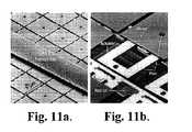
- FIG. 11 ais a photomicrograph of a TMA mirror array with a human hair superimposed to show scale
- FIG. 11 bshows the underlying actuator
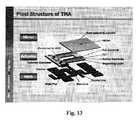
- FIG. 12is a schematic diagram of a TMA mirror array.
- FIG. 13is an exploded view of the TMA mirror array of FIG. 13 .
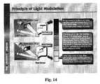
- FIG. 14illustrates the principle of light modulation by the TMA micromirror array.
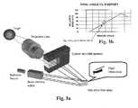
- FIG. 1shows a schematic diagram of a preferred embodiment 10 of the maskless laser beam apparatus of the present invention.
- the apparatusincludes a thin-film micromirror array 11 , an interface board 12 , a computer 14 , a computer input 16 , laser optics 18 , beam splitter 20 , re-imaging optics 22 , pattern detector and verifier 24 , feature location & end point detector 26 , and a laser 28 .
- a laser beam emanating from laser 28is split into a plurality of laser beamlets by laser optics 18 , and then modulated and reflected by individual micromirrors 11 a,b,c . . . through re-imaging optics 20 onto the surface of workpiece 30 .
- a key element of this apparatusis the thin-film micromirror 11 , which has a plurality of individual micromirrors 11 a,b,c . . . , each of which can be individually tilted with respect to incident laser beamlets as depicted in FIG. 1 .
- Individual control of the tilting of each micromirror 11 a,b,c . . .allows for modulation the energy of each beamlet before reflection onto the surface of workpiece 30 .
- the laser energyis substantially blocked from the imaging optics 22 .
- the mirror angleincreases the amount of energy directed toward the workpiece is increased, reaching a maximum at maximum tilt angle.
- FIG. 4is a graph of the relationship between energy intensity and typical ablation rate.
- each individual micromirror 11 a,b,c . . .is controlled by input 16 from computer 14 via an interface board 12 , to create a plurality of reflected beamlets having a defined spatial energy density distribution pattern.
- a series of different patternscan be sequentially imaged onto workpiece 30 to achieve a desired ablation pattern.
- a multi-layered structured workpiece 30 as illustrated in FIG. 5includes a base material 41 such as semiconductor material silicon or gallium arsenide, on top of which is a dielectric layer of silicon dioxide 42 . On top of the silicon dioxide is a covering layer 43 of polyimide. Other dielectric materials including silicon nitride and other polymeric materials maybe substituted for the various layers.
- FIG. 6illustrates how conventional UV mask exposures are performed to develop patterns using chemically processed photoresist. Etch patterns through the photoresist selectively expose silicon dioxide for further processing.
- the two layers 42 and 43are selectively ablated with little or no etching of the underlying base material 41 as shown in FIG. 6 .
- the polyimide layer 43is selectively ablated, exposing silicon dioxide 42 directly without chemical processing.
- FIG. 7shows how the ablation process in one area 44 can be terminated after removal of the polyimide layer 43 , while the ablation process can continue through the silicon dioxide layer 45 to the base material 41 in another area 45 , and that ablation can be terminated in this area with little or no etching of the underlying base material.
- FIG. 8is a perspective view of the resulting ablation etching in selective regions of the work piece.
- the well 47depicts the region 45 ablated through the polyimide layer 43 and silicon dioxide 42 layers of FIG. 6, while well 48 depicts the region selectively ablated through the polyimide layer 43 down to the silicon dioxide layer 42 .
- Polymeric materialsgenerally require relatively low ablation energy densities, e.g. around 200 mJ/cm 2 per pulse.
- Energy pulses with a width of about 20 ns and a repetition rate of 200 Hz to 20 KHztypically will have an etch rate of about 0.1 micron/pulse for polyimide.
- Silicon dioxide and silicon nitridehave significantly higher thresholds for ablation. Thus, energy densities of 600 mJ/cm 2 are typically required.
- An important part of this inventionis the termination of the process in localized areas at different layers to produce complex ablation patterns.
- the use of an addressable thin film micromirror array 11permits changing of the ablation etch pattern on successive laser pulses.
- the end point monitorwould detect and terminate the ablation etch process when the top layer is removed and the ablation etch process continued in the other area until the end point monitor terminated the process at the base material.
- Typical end point detection processes known in the art and of use in the present inventioninclude:
- FIG. 9illustrates a particular embodiment of the invention that accomplishes two dimensional translation of an energy source to track changes in the desired location of the energy application.
- the tracking techniqueincludes a method for identifying the location of the desired position for application of the energy and feeding back that location to the two dimensional tracking device.
- the energy sourceis shaped to produce the desired pattern for energy application at the desired location as described above in relation to FIG. 1 .
- the energy source 28is passed through a beam expander/homogenizer 18 to fill the field of the two dimensional micromirror array 11 , an area larger than the desired energy application area imaged on the work piece 30 .
- the computer 14sets only a portion of the micromirrors in the array to fill the desired two-dimensional shape required with the predetermined energy distribution.
- Alternate outline shapes of patterns on the work piececan be simple or complex and the energy distribution within boundaries of these patterns may be simple or complex as illustrated in FIG. 10 .
- the patterned image generated by micromirror 11is passed through the beam splitter 20 to the workpiece 30 .
- the reflected image pattern from the workpieceis reflected by the beam splitter 20 to the camera detector 26 which in turn feeds the image analyzer 50 .
- the workpiece index marks 32are also seen by the camera detector 26 and are similarly available to the image analyzer 50 .
- the image analyzer 50establishes the relative position of the workpiece 30 , index marks 32 , and an energy pattern such as one depicted in FIG. 10 . If the workpiece 30 shifts its position, the relative position of the workpiece index marks 32 and the energy pattern changes.
- This location change informationis fed to computer 14 , which in turn resets the micromirror array 11 to reposition the energy pattern on the work piece 30 to reduce the displacement relative to the work piece index marks to an acceptably small error or zero.
- Camera detector 24feeds the computer 14 , the image of the micromirror array 11 , from the beam splitter 20 , to analyze and confirm the position and predetermined energy pattern integrity.
- this electronic tracking system and pattern shaping inventiontrades source energy to accomplish tracking, i.e. if A 1 is the area of the energy pattern desired, and A 2 is the total area of the micromirror array illuminated by the source, the energy efficiency of the system is degraded by A 1 /A 2 .
- the key advantages of this approachinclude: that random energy application pattern shapes and rapid correction of location shifts can be accomplished much more rapidly than with conventional electromechanical systems.
- An alternate implementation of this inventionmounts the micromirrors on an electromechanical gimbal that is driven by the computer 14 to reduce the displacement relative to the workpiece index marks to an acceptably small error or zero.
- the advantage of this approachis to eliminate the efficiency loss cited above, since all of the energy illuminating the micromirrors is used within the predetermined pattern on the work piece.
- Thin-film micromirror arrays 11 suitable for use in the present inventionare made by Daewoo Electronics Co. Ltd. Korea under the trademark “Thin-film Micromirror Array (TMA).
- TMAThin-film Micromirror Array
- the TMA, thin-film micromirror array 11is an array of 1024 ⁇ 768 mirrors, each mirror measuring 49 microns ⁇ 49 microns, with a panel size of 2.54 inches diagonal.
- the TMAis a reflective spatial modulator used to modulate light in television video projection. It is a suitable device for the ablation patterning with appropriate modifications to operate at UV wavelengths including UV grade optics and UV reflective mirrors.
- Each TMA pixelis a monolithically integrated MEMS (Microelectromechanical Systems) device fabricated over a simple PMOS switch as illustrated in FIG. 11 a .
- the pixel size in this earlier versionis 97 microns by 97 microns.
- Each pixelconsists of a micromirror and an actuator as shown in FIG. 11 b .
- Each aluminum mirrorhas high reflectivity and excellent flatness for high optical efficiency, and the actuator has linear and fast response times, as well as mechanical and electrical reliability.
- micromirror array 1can be replaced by other reflective/transmissive mask devices including patterned foil devices.
- FIG. 12illustrates the TMA array structure.
- the TMAuses thin film piezoelectric actuators in the form of micro-cantilevers. As shown in FIG. 13, a mirror is connected to the cantilevers themselves through a support post. The cantilevers themselves are anchored to the underlying substrate.
- a cantileverconsists of the supporting layer, bottom electrode, piezoelectric layer, and top electrode. When an electric field is applied between the common electrode and the bottom electrode, the piezoelectric layer shrinks in the horizontal direction and expands in the vertical direction.
- FIG. 14shows the effect of tilting the mirror.
- the mirror deflection angledetermines the amount of light that pass through the modulation or optical stop.
- the piezoelectric materialoperates from 0 to 10 volts and the corresponding mirror deflection is from 0 to about 10 degrees.
- micromirror array 11may be substituted for other reflective mirror masks.
- Other micromirror array manufacturersinclude Texas Instruments and Standard MEMS.
- One such systemis a foil array of patterns, sequentially changed to modify the ablation etches on successive layers of a multi-layered structure as illustrated in FIGS. 7 and 8.
- the work piece 30may consist of tissue.
- tissue systemis an eye, whose corneal tissue is ablated to modify its refractive properties, e.g. photorefractive keratectomy.
Landscapes
- Physics & Mathematics (AREA)
- Optics & Photonics (AREA)
- Engineering & Computer Science (AREA)
- General Physics & Mathematics (AREA)
- Plasma & Fusion (AREA)
- Mechanical Engineering (AREA)
- Laser Beam Processing (AREA)
Abstract
Description
This application claims the priority of provisional U.S. Application Serial No. 60/207,041 filed on May 25, 2000 and entitled “A Maskiess Laser Beam Patterning Device and Apparatus for Ablation of Multilayered Structures with Continuous Monitoring of Ablation” by Jay J. Brandinger, the entire contents and substance of which are hereby incorporated in total by reference.
1. Field of the Invention
This invention relates to an apparatus and method for laser machine ablation to produce complex patterns suitable for the rapid and accurate patterning of one or more layers of material while not etching an underlying different material layer.
2. Description of Related Art
The use of ablation patterning of various materials including polymers is well known. U.S. Pat. No. 4,508,749, Brannon et al., for example, discloses the use of ultraviolet radiation for etching through a polyimide layer. This patent is aimed at producing tapered openings through the polyimide layer to expose an underlying metal layer so that an electrical connection can be made to the metal. U.S. Pat. No. 5,236,551, issued for Pan describes the use of ablation etching to pattern a polymetric material layer that is then used as a mask for etching patterns in an underlying metal layer with chemical etchants.
Polymeric materials have high absorptivity in the region, UV and limited thermal diffusivity, limiting spread of absorbed energy, and facilitating energy density build up in the desired volume of material, and explosion of the material when threshold is exceeded. The ablation process stops automatically when the low absorptive, high thermal diffusivity metallic layer is exposed. The above patents do not disclose the desirable ablation etching of low UV absorptive dielectric materials used in the manufacture of semiconductor devices, e.g. silicon dioxide and silicon nitride, which may also be used in combination with polyimides.
Ablation of low absorptive dielectric materials requires radiant energies approaching those needed to ablate metals, which in turn limits ablation process selectivity. This is the problem Mitwalsky et al. solved in U.S. Pat. No. 5,843,363 which describes ablation etching of a pattern through one or more dielectric layers overlying a conductive material to provide electrical contact access through aligned openings. The principle disclosed to terminate ablation at successive layers involves end point detection including monitoring material specific emission, changes in surface reflectivity, and material ions. Other methods described include predictive end points using a specific number of laser energy pulses, changing the absorptive characteristics of the dielectric material by changing the radiation wavelength, and darkening the material to increase absorption.
A limitation of the prior art inventions described above is the use of an electrically conductive metallic underlying layer and the use of physical masks to define ablation etch patterns. In many patterning processes the underlying base material is not metallic but the need to terminate ablation etching at intermediate layers of different materials is needed. Further, the creation of physical masks is time consuming and costly. Thus, there is a clear need for an economical, programmable system to rapidly create and change ablation patterns. There is also a need for a means to accomplish end point layer detection including time, layer thickness, reflectivity and quantity of material removal. An ability to flexibly arrange alternate material layers and to create arbitrary ablation patterns could significantly reduce process time and cost.
Briefly described, the invention comprises an apparatus and method for laser machine ablation to produce complex patterns suitable for the rapid and accurate patterning of one or more layers of material while not etching an underlying different material layer. The invention combines the functions of a programmable thin film micromirror array to produce a maskless pattern for material ablation and a monitoring system to rapidly correct workpiece positional errors and accurately control material removal.
The preprogrammed thin film micromirror array (TMA) has individually addressable and moveable mirrors capable of redistributing the laser output beam energy to produce a desired two-dimensional machining pattern. Simple and complex predetermined energy patterns can be created and rapidly changed. Different patterns can be generated on successive laser energy pulses both in energy distribution and geometric location, to create accurate, complex three-dimensional machining of a workpiece, not easily achieved by conventional machining techniques. An electronic tracking system is included to precisely align the laser energy patterns with workpiece features/indices and to continuously monitor the removal of material from the workpiece.
The invention may be more fully understood by reference to the following drawings.
FIG. 1 is a schematic diagram of a preferred embodiment of the ablation apparatus of the present invention.
FIG. 2 illustrates the operation of a single undeflected micromirror.
FIG. 3 illustrates the operation of a single partially deflected micromirror.
FIG. 4 illustrates the relationship between intensity and ablation rate.
FIG. 5 depicts a cross-section of a multi-layered workpiece prior to ablation.
FIG. 6 depicts the multi-layered work piece of FIG. 5 with the polyimide layer removed.
FIG. 7 illustrates different ablation patterns at different locations on the multilayered workpiece of FIG. 5 in contrast to a conventional process using photoresist.
FIG. 8 is a perspective drawing illustrating different ablation patterns at different locations on the multi-layered workpiece of FIG.5.
FIG. 9 is a schematic diagram depicting a electronic tracking system.
FIG. 10 illustrates three different complex patterns which can be created.
FIG. 11ais a photomicrograph of a TMA mirror array with a human hair superimposed to show scale
FIG. 11bshows the underlying actuator.
FIG. 12 is a schematic diagram of a TMA mirror array.
FIG. 13 is an exploded view of the TMA mirror array of FIG.13.
FIG. 14 illustrates the principle of light modulation by the TMA micromirror array.
During the course of this description like numbers will be used to identify like elements according to the different views that illustrate the invention.
FIG. 1 shows a schematic diagram of apreferred embodiment 10 of the maskless laser beam apparatus of the present invention. The apparatus includes a thin-film micromirror array 11, aninterface board 12, acomputer 14, acomputer input 16,laser optics 18,beam splitter 20,re-imaging optics 22, pattern detector andverifier 24, feature location &end point detector 26, and alaser 28. Operationally, a laser beam emanating fromlaser 28 is split into a plurality of laser beamlets bylaser optics 18, and then modulated and reflected by individual micromirrors11a,b,c. . . throughre-imaging optics 20 onto the surface ofworkpiece 30.
A key element of this apparatus is the thin-film micromirror 11, which has a plurality of individual micromirrors11a,b,c. . . , each of which can be individually tilted with respect to incident laser beamlets as depicted in FIG.1. Individual control of the tilting of each micromirror11a,b,c. . . allows for modulation the energy of each beamlet before reflection onto the surface ofworkpiece 30. When the mirror is not tilted, the laser energy is substantially blocked from theimaging optics 22. As the mirror angle increases the amount of energy directed toward the workpiece is increased, reaching a maximum at maximum tilt angle. The amount of energy that passes through to the work piece is linearly proportional to the tilt angle of each mirror as illustrated in FIGS. 2a,b(not tilted) &3a,b(partially tilted). FIG. 4 is a graph of the relationship between energy intensity and typical ablation rate.
The orientation of each individual micromirror11a,b,c. . . is controlled byinput 16 fromcomputer 14 via aninterface board 12, to create a plurality of reflected beamlets having a defined spatial energy density distribution pattern. A series of different patterns can be sequentially imaged ontoworkpiece 30 to achieve a desired ablation pattern.
A specific example of an ablation process as described above is illustrated in FIGS. 5-8. A multi-layered structuredworkpiece 30 as illustrated in FIG. 5 includes abase material 41 such as semiconductor material silicon or gallium arsenide, on top of which is a dielectric layer ofsilicon dioxide 42. On top of the silicon dioxide is acovering layer 43 of polyimide. Other dielectric materials including silicon nitride and other polymeric materials maybe substituted for the various layers.
FIG. 6 illustrates how conventional UV mask exposures are performed to develop patterns using chemically processed photoresist. Etch patterns through the photoresist selectively expose silicon dioxide for further processing. Using the ablation apparatus of the present invention, the twolayers underlying base material 41 as shown in FIG.6. as is also seen in FIG. 6, thepolyimide layer 43, is selectively ablated, exposingsilicon dioxide 42 directly without chemical processing.
FIG. 7 shows how the ablation process in onearea 44 can be terminated after removal of thepolyimide layer 43, while the ablation process can continue through thesilicon dioxide layer 45 to thebase material 41 in anotherarea 45, and that ablation can be terminated in this area with little or no etching of the underlying base material.
FIG. 8 is a perspective view of the resulting ablation etching in selective regions of the work piece. The well47 depicts theregion 45 ablated through thepolyimide layer 43 andsilicon dioxide 42 layers of FIG. 6, while well48 depicts the region selectively ablated through thepolyimide layer 43 down to thesilicon dioxide layer 42.
Polymeric materials generally require relatively low ablation energy densities, e.g. around 200 mJ/cm2per pulse. Energy pulses with a width of about 20 ns and a repetition rate of 200 Hz to 20 KHz typically will have an etch rate of about 0.1 micron/pulse for polyimide. Silicon dioxide and silicon nitride have significantly higher thresholds for ablation. Thus, energy densities of 600 mJ/cm2are typically required.
An important part of this invention is the termination of the process in localized areas at different layers to produce complex ablation patterns. The use of an addressable thinfilm micromirror array 11 permits changing of the ablation etch pattern on successive laser pulses. Thus, if in one area of the workpiece it is desired to remove only the top layer and in another area the removal of all layers down to the base material, the end point monitor would detect and terminate the ablation etch process when the top layer is removed and the ablation etch process continued in the other area until the end point monitor terminated the process at the base material.
Typical end point detection processes known in the art and of use in the present invention include:
1) establishing ablation time/pulses versus depth for specific deposited materials in the layers,
2) establishing depth of the ablated layer optically between laser pulses using surface reflection as compared with the measurement of the layer depth in unablated areas,
3) establishing changes in reflectivity at the boundary of dissimilar layer materials,
4) measuring the amount of material removal by measuring its re-deposition on another substrate,
5) measurement of changes in material composition spectroscopically,
6) using separately deposited layer materials with the same thickness and composition as that used on the work piece overlaying metallic base materials to monitor the ablation etch process.
FIG. 9 illustrates a particular embodiment of the invention that accomplishes two dimensional translation of an energy source to track changes in the desired location of the energy application. The tracking technique includes a method for identifying the location of the desired position for application of the energy and feeding back that location to the two dimensional tracking device. Separately, the energy source is shaped to produce the desired pattern for energy application at the desired location as described above in relation to FIG.1.
As shown in FIG. 9, theenergy source 28 is passed through a beam expander/homogenizer 18 to fill the field of the twodimensional micromirror array 11, an area larger than the desired energy application area imaged on thework piece 30. Thecomputer 14 sets only a portion of the micromirrors in the array to fill the desired two-dimensional shape required with the predetermined energy distribution. Alternate outline shapes of patterns on the work piece can be simple or complex and the energy distribution within boundaries of these patterns may be simple or complex as illustrated in FIG.10.
The patterned image generated bymicromirror 11 is passed through thebeam splitter 20 to theworkpiece 30. The reflected image pattern from the workpiece is reflected by thebeam splitter 20 to thecamera detector 26 which in turn feeds theimage analyzer 50. The workpiece index marks32 are also seen by thecamera detector 26 and are similarly available to theimage analyzer 50. Theimage analyzer 50 establishes the relative position of theworkpiece 30, index marks32, and an energy pattern such as one depicted in FIG.10. If theworkpiece 30 shifts its position, the relative position of the workpiece index marks32 and the energy pattern changes. This location change information is fed tocomputer 14, which in turn resets themicromirror array 11 to reposition the energy pattern on thework piece 30 to reduce the displacement relative to the work piece index marks to an acceptably small error or zero.Camera detector 24 feeds thecomputer 14, the image of themicromirror array 11, from thebeam splitter 20, to analyze and confirm the position and predetermined energy pattern integrity.
It should be noted that this electronic tracking system and pattern shaping invention trades source energy to accomplish tracking, i.e. if A1is the area of the energy pattern desired, and A2is the total area of the micromirror array illuminated by the source, the energy efficiency of the system is degraded by A1/A2. The key advantages of this approach include: that random energy application pattern shapes and rapid correction of location shifts can be accomplished much more rapidly than with conventional electromechanical systems.
An alternate implementation of this invention mounts the micromirrors on an electromechanical gimbal that is driven by thecomputer 14 to reduce the displacement relative to the workpiece index marks to an acceptably small error or zero. The advantage of this approach is to eliminate the efficiency loss cited above, since all of the energy illuminating the micromirrors is used within the predetermined pattern on the work piece.
Similarly, it is possible to accomplish the tracking by using other eletromechanical means including galvanometer mirror systems, and solenoid actuators.
Thin-film micromirror arrays 11 suitable for use in the present invention are made by Daewoo Electronics Co. Ltd. Korea under the trademark “Thin-film Micromirror Array (TMA).
The TMA, thin-film micromirror array 11, is an array of 1024×768 mirrors, each mirror measuring 49 microns×49 microns, with a panel size of 2.54 inches diagonal. The TMA is a reflective spatial modulator used to modulate light in television video projection. It is a suitable device for the ablation patterning with appropriate modifications to operate at UV wavelengths including UV grade optics and UV reflective mirrors.
Each TMA pixel is a monolithically integrated MEMS (Microelectromechanical Systems) device fabricated over a simple PMOS switch as illustrated in FIG. 11a. The pixel size in this earlier version is 97 microns by 97 microns. Each pixel consists of a micromirror and an actuator as shown in FIG. 11b. Each aluminum mirror has high reflectivity and excellent flatness for high optical efficiency, and the actuator has linear and fast response times, as well as mechanical and electrical reliability. It is also understood that micromirror array1 can be replaced by other reflective/transmissive mask devices including patterned foil devices. FIG. 12 illustrates the TMA array structure.
The TMA uses thin film piezoelectric actuators in the form of micro-cantilevers. As shown in FIG. 13, a mirror is connected to the cantilevers themselves through a support post. The cantilevers themselves are anchored to the underlying substrate. A cantilever consists of the supporting layer, bottom electrode, piezoelectric layer, and top electrode. When an electric field is applied between the common electrode and the bottom electrode, the piezoelectric layer shrinks in the horizontal direction and expands in the vertical direction.
Since the neutral plane of the cantilever shifts toward the bottom of the electrode due to thickness of the supporting layer, the mechanical strain of the piezoelectric layer causes vertical deflection of the cantilever and a tilt of the mirror on top of it. FIG. 14 shows the effect of tilting the mirror. When there is no tilt, no light goes out of the modulation stop and when maximum defection of the mirror is achieved, the maximum amount of light is passed by the modulation stop. FIGS. 2 and 3 detail the operation of one pixel in the undeflected and partially deflected positions. As is shown in graph2b, the mirror deflection angle determines the amount of light that pass through the modulation or optical stop. In the case of the TMA, the piezoelectric material operates from 0 to 10 volts and the corresponding mirror deflection is from 0 to about 10 degrees.
It is also understood that other reflective mirror masks may be substituted for themicromirror array 11. Other micromirror array manufacturers include Texas Instruments and Standard MEMS. One such system is a foil array of patterns, sequentially changed to modify the ablation etches on successive layers of a multi-layered structure as illustrated in FIGS. 7 and 8. It is also understood that thework piece 30 may consist of tissue. One such tissue system is an eye, whose corneal tissue is ablated to modify its refractive properties, e.g. photorefractive keratectomy.
While the invention has been described with reference to the preferred embodiment thereof, it will be appreciated by those of ordinary skill in the art that modifications can be made to the structure and elements of the invention without departing from the spirit and scope of the invention as a whole.
Claims (13)
1. A process for machining a multi-layered work piece comprising at least a base layer, and a first layer of material of a dissimilar material on the surface of said base layer and preferably, a second layer of material of a dissimilar material to said first layer, said process consisting of the steps of:
(a) ablation etching a complex, three-dimensional pattern of openings into said work piece by directing radiant energy of a given energy against said composite work piece;
(b) generating, by using a computer, a maskless complex pattern and projecting said pattern onto said work piece using a Digital Micro Device (DMD) micromirror structure;
(c) continuously monitoring selected parameters from said work piece; and,
(d) selectively terminating said ablation etching in at least one localized area, in accordance with said complex pattern, upon reaching the predetermined level of material removal in said localized area as detected in said monitoring step, thereby allowing said ablation etching to be selectively stopped upon reaching said predetermined level, independent of process conditions, while continuing ablation etching in at least another localized area to form said three-dimensional pattern of openings,
whereby said complex three-dimensional pattern of openings is etched into said work piece.
2. The process according toclaim 1 wherein said monitoring step consists of:
detecting changes as a function of time, in a parameter selected from the group consisting of depth of layer, change in reflectivity of layer and quantity of material deposited on surrounding area.
3. The process according toclaim 2 wherein said step of selectively terminating said ablation etching comprises the step of:
discontinuing the directing of radiant energy against the work piece within said at least one localized area.
4. The process according toclaim 3 wherein said first layer material is selected from the group consisting of silicon dioxide and silicon nitride.
5. The process according toclaim 4 wherein said second layer is a non-polymeric material.
6. A process for maskless, complex, pattern machining of a multi-layered work piece comprising at least a base layer, and a first layer of material of a dissimilar material on the surface of said base layer and preferably, a second layer of material of a dissimilar material to said first layer, said process consisting of the steps of:
(a) ablation etching a three-dimensional pattern of openings partway into said work piece by directing an ablation etch pattern of radiant energy of a first energy level against said multi-layered work piece, using a computer addressable micromirror array;
(b) providing a second beam of incident energy with an energy level sufficiently low so as to prevent ablation;
(e) continuously monitoring said work piece, using said second beam, with a detector located so as to determine the desired depth of ablation;
(f) calculating, using a computer, the differences between the measured depth of ablation and the desired ablation; and
(g) selectively stopping said ablation etching in at least one localized area upon reaching a desired depth of ablation in said localized area, by changing said ablation etch pattern using said addressable micromirror array, while continuing ablation etching in at least another localized area,
whereby said three-dimensional pattern of openings is etched in said surface of said work piece.
7. The process according toclaim 6 wherein said first energy level of said first beam of radiant energy is sufficiently high for ablation etching of said base layer of said work piece.
8. The process according toclaim 7 wherein said work piece is comprised of an additional layer overlying said first layer prior to said ablation etching and wherein said ablation etching creates openings through both said first layer and said overlying layer.
9. The process according toclaim 6 wherein said step of directing an ablation etch pattern of radiant energy of a first energy level against said work piece, using a computer addressable micromirror array wherein said computer is programmable and said micromirror array mirrors are individually addressable and movable mirrors, programmed to produce the desired array pattern for ablation etching said composite work piece.
10. The process according toclaim 9 wherein said directing said radiant energy against said composite work piece includes the use of a programmable modulating apparatus including a computer connected to a high resolution light valve or switch arrays having individually addressable elements, programmed to produce the desired array pattern for ablation etching said composite work piece.
11. The process according toclaim 10 wherein said step of directing said radiant energy against said work piece further including the step of: moving a said beam of radiant energy across said work piece in discrete steps.
12. A process for pattern machining a multi-layered work piece comprising at least a base layer, and a first layer of material of dissimilar material on the surface said base layer and preferably, a second layer of material of a dissimilar material to said first layer, said process consisting of the steps of:
(a) ablation etching a three-dimensional pattern of openings into said work by, directing a first beam of radiant energy having a first energy level and a first ablation pattern against said work piece;
(b) directing a second beam of radiant energy with a second wavelength different from than said wavelength of said first beam of radiant energy incident on said composite work piece and with a second energy level which is below the ablation threshold to monitor the quantity and rate of material removal from said work piece;
(c) monitoring the quantity of material removal from said work piece to ascertain when said ablation etching process reaches said first layer;
(d) monitoring the rate of material removal from said work piece to ascertain when said ablation etching process reaches said first layer;
(e) altering said first ablation pattern to a second ablation pattern upon reaching said first layer, wherein said second ablation pattern selectively stops further ablation etching within at least one region of said first ablation pattern;
(f) monitoring the quantity of material removal from said work piece to ascertain when said ablation etching process reaches said base layer;
(g) monitoring the rate of material removal from said work piece to ascertain when said ablation etching process reaches said base layer; and,
(h) stopping said ablation etching upon reaching said base layer, while continuing ablation etching in at least another region,
whereby said three-dimensional pattern of openings is etched in said surface of said work piece.
13. A process for machining a multi-layered work piece comprising at least a base layer, and a first layer of material of a dissimilar material on the surface of said base layer and preferably, a second layer of material of a dissimilar material to said first layer, said process consisting of the steps of:
(a) monitoring selected parameters from said work piece;
(b) generating a working complex pattern of radiation, said working complex pattern of radiation being formed from a source of radiant energy by an addressable Digital Micro Device (DMD) micromirror structure under control of a computer using said monitoring selected parameters;
(c) ablation etching said working complex pattern of radiation into said work piece by projecting said working complex pattern of radiation onto said work piece; and,
(d) repeating said steps of monitoring, generating and ablation etching, wherein said working pattern of radiation is generated such that said step of ablation etching is selectively terminated in at least one localized region of said desired pattern upon reaching a predetermined level of material removal in said localized region, as detected in said monitoring step, while continuing ablation etching in at least another localized region to another predetermined level of material removal until a desired three-dimensional pattern is etched into said work piece.
Priority Applications (1)
| Application Number | Priority Date | Filing Date | Title |
|---|---|---|---|
| US09/865,939US6696008B2 (en) | 2000-05-25 | 2001-05-25 | Maskless laser beam patterning ablation of multilayered structures with continuous monitoring of ablation |
Applications Claiming Priority (2)
| Application Number | Priority Date | Filing Date | Title |
|---|---|---|---|
| US20704100P | 2000-05-25 | 2000-05-25 | |
| US09/865,939US6696008B2 (en) | 2000-05-25 | 2001-05-25 | Maskless laser beam patterning ablation of multilayered structures with continuous monitoring of ablation |
Publications (2)
| Publication Number | Publication Date |
|---|---|
| US20010045690A1 US20010045690A1 (en) | 2001-11-29 |
| US6696008B2true US6696008B2 (en) | 2004-02-24 |
Family
ID=26901905
Family Applications (1)
| Application Number | Title | Priority Date | Filing Date |
|---|---|---|---|
| US09/865,939Expired - Fee RelatedUS6696008B2 (en) | 2000-05-25 | 2001-05-25 | Maskless laser beam patterning ablation of multilayered structures with continuous monitoring of ablation |
Country Status (1)
| Country | Link |
|---|---|
| US (1) | US6696008B2 (en) |
Cited By (83)
| Publication number | Priority date | Publication date | Assignee | Title |
|---|---|---|---|---|
| US20020196534A1 (en)* | 2001-06-19 | 2002-12-26 | Lizotte Todd E. | Laser beam delivery system with trepanning module |
| US20030094367A1 (en)* | 2000-11-01 | 2003-05-22 | Bhullar Raghbir S. | Biosensor |
| US20030179452A1 (en)* | 2002-03-18 | 2003-09-25 | Lizotte Todd E. | Beam or wave front |
| US20040163953A1 (en)* | 2000-10-06 | 2004-08-26 | Bhullar Raghbir S. | Biosensor |
| US20040194302A1 (en)* | 1999-10-04 | 2004-10-07 | Bhullar Raghbir S. | Method of making a biosensor |
| US20040200815A1 (en)* | 2003-04-10 | 2004-10-14 | Lizotte Todd E. | System and method for generating and controlling multiple independently steerable laser beam for material processing |
| US20040251243A1 (en)* | 2003-04-10 | 2004-12-16 | Lizotte Todd E. | System and method for generating and controlling multiple independently steerable laser beams for material processing |
| US20050056626A1 (en)* | 2003-09-12 | 2005-03-17 | Orbotech Ltd | Multiple beam micro-machining system and method |
| US20050068510A1 (en)* | 2003-09-22 | 2005-03-31 | Asml Netherlands B.V. | Lithographic apparatus and device manufacturing method |
| US20050074906A1 (en)* | 2003-10-03 | 2005-04-07 | Asml Holding N.V. | Method and systems for total focus deviation adjustments on maskless lithography systems |
| US20050230368A1 (en)* | 2004-03-31 | 2005-10-20 | Matsushita Electric Industrial Co., Ltd. | System for and method of manufacturing gravure printing plates |
| US20060000812A1 (en)* | 2004-07-02 | 2006-01-05 | Jan Weber | Method and apparatus for controlling and adjusting the intensity profile of a laser beam employed in a laser welder for welding polymeric and metallic components |
| US20060046461A1 (en)* | 2004-09-01 | 2006-03-02 | Benson Peter A | Method for creating electrically conductive elements for semiconductor device structures using laser ablation processes and methods of fabricating semiconductor device assemblies |
| US20060084957A1 (en)* | 2003-08-11 | 2006-04-20 | Peter Delfyett | Laser ablation method and apparatus having a feedback loop and control unit |
| US20060082752A1 (en)* | 2004-10-18 | 2006-04-20 | Asml Netherlands B.V. | Lithographic apparatus and device manufacturing method |
| US20060108327A1 (en)* | 2004-11-23 | 2006-05-25 | Chng Kiong C | Method of manufacturing a microstructure |
| US20060278681A1 (en)* | 2005-06-03 | 2006-12-14 | Viola Frank J | Battery powered surgical instrument |
| US20060278680A1 (en)* | 2005-06-03 | 2006-12-14 | Viola Frank J | Surgical stapler with timer and feedback display |
| US20070114700A1 (en)* | 2005-11-22 | 2007-05-24 | Andrewlavage Edward F Jr | Apparatus, system and method for manufacturing a plugging mask for a honeycomb substrate |
| US20070253455A1 (en)* | 2006-04-26 | 2007-11-01 | Stadler Andrew D | Intelligent Laser Interlock System |
| US20080083715A1 (en)* | 2006-10-05 | 2008-04-10 | Mu-Gahat Enterprises, L.L.C. | Reverse side film laser circuit etching |
| US20080083706A1 (en)* | 2006-10-05 | 2008-04-10 | Mu-Gahat Enterprises, Llc | Reverse side film laser circuit etching |
| US20080140060A1 (en)* | 2003-08-11 | 2008-06-12 | Raydiance, Inc. | Ablative material removal with a preset removal rate or volume or depth |
| US20080251568A1 (en)* | 2007-04-13 | 2008-10-16 | Michael Zemlok | Powered surgical instrument |
| US20080272172A1 (en)* | 2007-05-01 | 2008-11-06 | Michael Zemlok | Powered surgical stapling device platform |
| US20080314882A1 (en)* | 2001-08-29 | 2008-12-25 | Bhullar Raghbir S | Method of making a biosensor |
| US20090001129A1 (en)* | 2007-03-15 | 2009-01-01 | Stanislaw Marczyk | Surgical stapling apparatus with powered articulation |
| US20090061112A1 (en)* | 2007-08-27 | 2009-03-05 | Mu-Gahat Enterprises, Llc | Laser circuit etching by subtractive deposition |
| US20090061251A1 (en)* | 2007-08-27 | 2009-03-05 | Mu-Gahat Enterprises, Llc | Laser circuit etching by additive deposition |
| US20090289382A1 (en)* | 2008-05-22 | 2009-11-26 | Raydiance, Inc. | System and method for modifying characteristics of a contact lens utilizing an ultra-short pulsed laser |
| US20090323740A1 (en)* | 2006-01-23 | 2009-12-31 | Stadler Andrew D | Systems And Methods For Control Of Ultra Short Pulse Amplification |
| US20100040095A1 (en)* | 2008-08-18 | 2010-02-18 | Raydiance, Inc. | Systems and methods for controlling a pulsed laser by combining laser signals |
| US20100312257A1 (en)* | 2009-06-08 | 2010-12-09 | Tyco Healthcare Group Lp | Powered tack applier |
| US7892849B2 (en) | 2003-06-20 | 2011-02-22 | Roche Diagnostics Operations, Inc. | Reagent stripe for test strip |
| US7893384B2 (en) | 2004-12-07 | 2011-02-22 | Chosen Technologies, Inc. | Systems and methods for laser material manipulation |
| US20110073584A1 (en)* | 2003-05-20 | 2011-03-31 | Richard Stoltz | Portable Optical Ablation System |
| US7922063B2 (en) | 2007-10-31 | 2011-04-12 | Tyco Healthcare Group, Lp | Powered surgical instrument |
| US7931660B2 (en) | 2007-05-10 | 2011-04-26 | Tyco Healthcare Group Lp | Powered tacker instrument |
| US20110116518A1 (en)* | 2008-05-02 | 2011-05-19 | Trumpf Laser- Und Systemtechnik Gmbh | Dynamic Redirection of a Laser Beam |
| US20120037609A1 (en)* | 2010-08-12 | 2012-02-16 | David Gaudiosi | Polymer tubing laser micromachining |
| US8135050B1 (en) | 2005-07-19 | 2012-03-13 | Raydiance, Inc. | Automated polarization correction |
| US8150271B1 (en) | 2006-03-28 | 2012-04-03 | Raydiance, Inc. | Active tuning of temporal dispersion in an ultrashort pulse laser system |
| US8173929B1 (en)* | 2003-08-11 | 2012-05-08 | Raydiance, Inc. | Methods and systems for trimming circuits |
| US8189971B1 (en) | 2006-01-23 | 2012-05-29 | Raydiance, Inc. | Dispersion compensation in a chirped pulse amplification system |
| USRE43487E1 (en) | 2000-09-20 | 2012-06-26 | Electro Scientific Industries, Inc. | Laser segmented cutting |
| US20130155404A1 (en)* | 2011-12-14 | 2013-06-20 | Gwangju Institute Of Science And Technology | System for real-time analysis of material distribution in cigs thin film using laser-induced breakdown spectroscopy |
| US8800837B2 (en) | 2007-04-13 | 2014-08-12 | Covidien Lp | Powered surgical instrument |
| US8853577B1 (en)* | 2012-08-08 | 2014-10-07 | Google Inc. | Keycap for use in backlit keyboards |
| US8921733B2 (en) | 2003-08-11 | 2014-12-30 | Raydiance, Inc. | Methods and systems for trimming circuits |
| US9114482B2 (en) | 2010-09-16 | 2015-08-25 | Raydiance, Inc. | Laser based processing of layered materials |
| US9130344B2 (en) | 2006-01-23 | 2015-09-08 | Raydiance, Inc. | Automated laser tuning |
| EP2352618A4 (en)* | 2008-10-10 | 2017-04-05 | IPG Microsystems LLC | Laser machining systems and methods with multiple beamlet laser beam delivery systems |
| US10239160B2 (en) | 2011-09-21 | 2019-03-26 | Coherent, Inc. | Systems and processes that singulate materials |
| US10285694B2 (en) | 2001-10-20 | 2019-05-14 | Covidien Lp | Surgical stapler with timer and feedback display |
| US10524785B2 (en) | 2007-04-13 | 2020-01-07 | Covidien Lp | Powered surgical instrument |
| US10987104B2 (en) | 2017-10-30 | 2021-04-27 | Covidien Lp | Apparatus for endoscopic procedures |
| US11197734B2 (en) | 2018-10-30 | 2021-12-14 | Covidien Lp | Load sensing devices for use in surgical instruments |
| US11202635B2 (en) | 2019-02-04 | 2021-12-21 | Covidien Lp | Programmable distal tilt position of end effector for powered surgical devices |
| US11207066B2 (en) | 2017-10-30 | 2021-12-28 | Covidien Lp | Apparatus for endoscopic procedures |
| US11219461B2 (en) | 2019-03-08 | 2022-01-11 | Covidien Lp | Strain gauge stabilization in a surgical device |
| US11259802B2 (en) | 2007-04-13 | 2022-03-01 | Covidien Lp | Powered surgical instrument |
| US11291443B2 (en) | 2005-06-03 | 2022-04-05 | Covidien Lp | Surgical stapler with timer and feedback display |
| US11311295B2 (en) | 2017-05-15 | 2022-04-26 | Covidien Lp | Adaptive powered stapling algorithm with calibration factor |
| US11369372B2 (en) | 2018-11-28 | 2022-06-28 | Covidien Lp | Surgical stapler adapter with flexible cable assembly, flexible fingers, and contact clips |
| US11376006B2 (en) | 2019-02-06 | 2022-07-05 | Covidien Lp | End effector force measurement with digital drive circuit |
| US11458244B2 (en) | 2020-02-07 | 2022-10-04 | Covidien Lp | Irrigating surgical apparatus with positive pressure fluid |
| US11497490B2 (en) | 2018-07-09 | 2022-11-15 | Covidien Lp | Powered surgical devices including predictive motor control |
| US11553913B2 (en) | 2020-02-11 | 2023-01-17 | Covidien Lp | Electrically-determining tissue cut with surgical stapling apparatus |
| US11622768B2 (en) | 2020-07-13 | 2023-04-11 | Covidien Lp | Methods and structure for confirming proper assembly of powered surgical stapling systems |
| US11653919B2 (en) | 2020-11-24 | 2023-05-23 | Covidien Lp | Stapler line reinforcement continuity |
| US11684362B2 (en) | 2021-06-07 | 2023-06-27 | Covidien Lp | Handheld electromechanical surgical system |
| WO2023155549A1 (en)* | 2022-11-28 | 2023-08-24 | 精捷科技光学股份有限公司 | Laser removal solder mask layer processing method for substrate |
| US11744580B2 (en) | 2020-11-24 | 2023-09-05 | Covidien Lp | Long stapler reloads with continuous cartridge |
| US11771432B2 (en) | 2021-06-29 | 2023-10-03 | Covidien Lp | Stapling and cutting to default values in the event of strain gauge data integrity loss |
| US11832823B2 (en) | 2022-02-08 | 2023-12-05 | Covidien Lp | Determination of anvil release during anastomosis |
| US12016556B2 (en) | 2021-05-03 | 2024-06-25 | Covidien Lp | Handheld electromechanical surgical system |
| KR20240103618A (en)* | 2022-12-27 | 2024-07-04 | 트릴리온 하비스트 리미티드 | Manufacturing Method by Laser Cutting Process of Solder Mask on Substrate |
| US12029470B2 (en) | 2020-05-21 | 2024-07-09 | Covidien Lp | Simultaneous RF monopolar calibration using a shared return electrode |
| US12137902B2 (en) | 2018-07-25 | 2024-11-12 | Covidien Lp | Adaptive anti-twitch algorithm for powered surgical devices |
| US12161341B2 (en) | 2021-09-07 | 2024-12-10 | Covidien Lp | Slow speed staple and staple relaxation for stapling optimization |
| US12185949B2 (en) | 2017-10-30 | 2025-01-07 | Covidien Lp | Apparatus for endoscopic procedures |
| US12193884B2 (en) | 2020-11-17 | 2025-01-14 | Covidien Lp | Contactless force measurement of motor torque in powered surgical device |
| US12276784B2 (en) | 2019-08-19 | 2025-04-15 | Asml Netherlands B.V. | Micromirror arrays |
Families Citing this family (26)
| Publication number | Priority date | Publication date | Assignee | Title |
|---|---|---|---|---|
| US6566627B2 (en)* | 2000-08-11 | 2003-05-20 | Westar Photonics, Inc. | Laser method for shaping of optical lenses |
| JP2004514285A (en)* | 2000-11-17 | 2004-05-13 | エムコア・コーポレイション | Laser isolation die with tapered sidewalls to improve light extraction |
| WO2002101888A2 (en)* | 2001-06-13 | 2002-12-19 | Orbotech Ltd. | Multi-beam micro-machining system and method |
| TWI265550B (en)* | 2002-05-14 | 2006-11-01 | Toshiba Corp | Fabrication method, manufacturing method for semiconductor device, and fabrication device |
| EP1482375B1 (en)* | 2003-05-30 | 2014-09-17 | ASML Netherlands B.V. | Lithographic apparatus and device manufacturing method |
| EP1482373A1 (en)* | 2003-05-30 | 2004-12-01 | ASML Netherlands B.V. | Lithographic apparatus and device manufacturing method |
| SG110099A1 (en)* | 2003-06-24 | 2005-04-28 | Asml Holding Nv | Projection optical system for maskless lithography |
| US7110082B2 (en)* | 2003-06-24 | 2006-09-19 | Asml Holding N.V. | Optical system for maskless lithography |
| JP4766874B2 (en)* | 2004-01-14 | 2011-09-07 | 臼井国際産業株式会社 | Method for removing resin layer of resin-coated metal tube |
| US8057963B2 (en)* | 2004-06-10 | 2011-11-15 | Lsi Corporation | Maskless vortex phase shift optical direct write lithography |
| US7170584B2 (en)* | 2004-11-17 | 2007-01-30 | Asml Netherlands B.V. | Lithographic apparatus and device manufacturing method |
| US7400382B2 (en)* | 2005-04-28 | 2008-07-15 | Asml Holding N.V. | Light patterning device using tilting mirrors in a superpixel form |
| GB0509213D0 (en)* | 2005-05-04 | 2005-06-15 | Univ Durham | A method for creating a chemically patterned surface |
| US20100071765A1 (en)* | 2008-09-19 | 2010-03-25 | Peter Cousins | Method for fabricating a solar cell using a direct-pattern pin-hole-free masking layer |
| KR20100110996A (en)* | 2009-04-06 | 2010-10-14 | 주식회사 프로텍 | Method for adjusting laser beam pitch by controlling of movement for both grid image and a tilting angle of a stage |
| JP2011102230A (en)* | 2009-10-13 | 2011-05-26 | Canon Inc | Method of notching brittle material, method of making member having notch, and method of making display device |
| US9409252B2 (en)* | 2010-03-26 | 2016-08-09 | Waters Technologies Corporation | Chromatography apparatus having diffusion-bonded and surface-modified components |
| CN102510788B (en)* | 2010-06-14 | 2014-12-24 | 三菱电机株式会社 | Laser processing device and laser processing method |
| US9703207B1 (en)* | 2011-07-08 | 2017-07-11 | Kla-Tencor Corporation | System and method for reducing dynamic range in images of patterned regions of semiconductor wafers |
| US20140263219A1 (en)* | 2013-03-15 | 2014-09-18 | Abbott Cardiovascular Systems Inc. | Laser optics with lateral and angular shift compensation |
| DE102013207243B4 (en)* | 2013-04-22 | 2019-10-02 | Fraunhofer-Gesellschaft zur Förderung der angewandten Forschung e.V. | DEVICE AND METHOD FOR PRODUCING A STRUCTURE OF CURABLE MATERIAL BY IMPREGNATION |
| KR102171301B1 (en)* | 2013-07-09 | 2020-10-29 | 삼성디스플레이 주식회사 | Digital exposure device using dmd and control method thereof |
| CN109746570B (en)* | 2019-02-26 | 2021-08-17 | 苏州创鑫激光科技有限公司 | Light power attenuation adjusting system and method and laser welding system |
| CN112044874B (en)* | 2020-09-27 | 2022-02-25 | 厦门理工学院 | A real-time monitoring system and monitoring method for laser cleaning |
| EP4555382A1 (en)* | 2022-07-12 | 2025-05-21 | ASML Netherlands B.V. | Mirror assembly for micromirror array |
| CN117697166B (en)* | 2024-02-06 | 2024-04-19 | 中国工程物理研究院激光聚变研究中心 | Method for etching organic film on surface of metal film by utilizing laser |
Citations (12)
| Publication number | Priority date | Publication date | Assignee | Title |
|---|---|---|---|---|
| US4508749A (en) | 1983-12-27 | 1985-04-02 | International Business Machines Corporation | Patterning of polyimide films with ultraviolet light |
| US5236551A (en) | 1990-05-10 | 1993-08-17 | Microelectronics And Computer Technology Corporation | Rework of polymeric dielectric electrical interconnect by laser photoablation |
| US5286947A (en)* | 1992-09-08 | 1994-02-15 | General Electric Company | Apparatus and method for monitoring material removal from a workpiece |
| US5593606A (en)* | 1994-07-18 | 1997-01-14 | Electro Scientific Industries, Inc. | Ultraviolet laser system and method for forming vias in multi-layered targets |
| US5691541A (en)* | 1996-05-14 | 1997-11-25 | The Regents Of The University Of California | Maskless, reticle-free, lithography |
| US5841099A (en)* | 1994-07-18 | 1998-11-24 | Electro Scientific Industries, Inc. | Method employing UV laser pulses of varied energy density to form depthwise self-limiting blind vias in multilayered targets |
| US5843363A (en)* | 1995-03-31 | 1998-12-01 | Siemens Aktiengesellschaft | Ablation patterning of multi-layered structures |
| US6037564A (en)* | 1998-03-31 | 2000-03-14 | Matsushita Electric Industrial Co., Ltd. | Method for scanning a beam and an apparatus therefor |
| US6103992A (en)* | 1996-11-08 | 2000-08-15 | W. L. Gore & Associates, Inc. | Multiple frequency processing to minimize manufacturing variability of high aspect ratio micro through-vias |
| US6215094B1 (en)* | 1993-10-01 | 2001-04-10 | Universitat Stuttgart | Process for determining the instantaneous penetration depth and a machining laser beam into a workpiece, and device for implementing this process |
| US6407363B2 (en)* | 2000-03-30 | 2002-06-18 | Electro Scientific Industries, Inc. | Laser system and method for single press micromachining of multilayer workpieces |
| US6441337B1 (en)* | 1997-12-12 | 2002-08-27 | Matsushita Electric Industrial Co., Ltd. | Laser machining method, laser machining device and control method of laser machining |
- 2001
- 2001-05-25USUS09/865,939patent/US6696008B2/ennot_activeExpired - Fee Related
Patent Citations (12)
| Publication number | Priority date | Publication date | Assignee | Title |
|---|---|---|---|---|
| US4508749A (en) | 1983-12-27 | 1985-04-02 | International Business Machines Corporation | Patterning of polyimide films with ultraviolet light |
| US5236551A (en) | 1990-05-10 | 1993-08-17 | Microelectronics And Computer Technology Corporation | Rework of polymeric dielectric electrical interconnect by laser photoablation |
| US5286947A (en)* | 1992-09-08 | 1994-02-15 | General Electric Company | Apparatus and method for monitoring material removal from a workpiece |
| US6215094B1 (en)* | 1993-10-01 | 2001-04-10 | Universitat Stuttgart | Process for determining the instantaneous penetration depth and a machining laser beam into a workpiece, and device for implementing this process |
| US5593606A (en)* | 1994-07-18 | 1997-01-14 | Electro Scientific Industries, Inc. | Ultraviolet laser system and method for forming vias in multi-layered targets |
| US5841099A (en)* | 1994-07-18 | 1998-11-24 | Electro Scientific Industries, Inc. | Method employing UV laser pulses of varied energy density to form depthwise self-limiting blind vias in multilayered targets |
| US5843363A (en)* | 1995-03-31 | 1998-12-01 | Siemens Aktiengesellschaft | Ablation patterning of multi-layered structures |
| US5691541A (en)* | 1996-05-14 | 1997-11-25 | The Regents Of The University Of California | Maskless, reticle-free, lithography |
| US6103992A (en)* | 1996-11-08 | 2000-08-15 | W. L. Gore & Associates, Inc. | Multiple frequency processing to minimize manufacturing variability of high aspect ratio micro through-vias |
| US6441337B1 (en)* | 1997-12-12 | 2002-08-27 | Matsushita Electric Industrial Co., Ltd. | Laser machining method, laser machining device and control method of laser machining |
| US6037564A (en)* | 1998-03-31 | 2000-03-14 | Matsushita Electric Industrial Co., Ltd. | Method for scanning a beam and an apparatus therefor |
| US6407363B2 (en)* | 2000-03-30 | 2002-06-18 | Electro Scientific Industries, Inc. | Laser system and method for single press micromachining of multilayer workpieces |
Cited By (197)
| Publication number | Priority date | Publication date | Assignee | Title |
|---|---|---|---|---|
| US20040194302A1 (en)* | 1999-10-04 | 2004-10-07 | Bhullar Raghbir S. | Method of making a biosensor |
| US7386937B2 (en) | 1999-10-04 | 2008-06-17 | Roche Diagnostics Operations, Inc. | Method of making a biosensor |
| US7073246B2 (en) | 1999-10-04 | 2006-07-11 | Roche Diagnostics Operations, Inc. | Method of making a biosensor |
| USRE43605E1 (en) | 2000-09-20 | 2012-08-28 | Electro Scientific Industries, Inc. | Laser segmented cutting, multi-step cutting, or both |
| USRE43487E1 (en) | 2000-09-20 | 2012-06-26 | Electro Scientific Industries, Inc. | Laser segmented cutting |
| US20040163953A1 (en)* | 2000-10-06 | 2004-08-26 | Bhullar Raghbir S. | Biosensor |
| US7287318B2 (en) | 2000-10-06 | 2007-10-30 | Roche Diagnostics Operations, Inc. | Biosensor |
| US20030094367A1 (en)* | 2000-11-01 | 2003-05-22 | Bhullar Raghbir S. | Biosensor |
| US6911621B2 (en) | 2000-11-01 | 2005-06-28 | Roche Diagnostics Corporation | Biosensor |
| US20020196534A1 (en)* | 2001-06-19 | 2002-12-26 | Lizotte Todd E. | Laser beam delivery system with trepanning module |
| US6804269B2 (en) | 2001-06-19 | 2004-10-12 | Hitachi Via Mechanics, Ltd. | Laser beam delivery system with trepanning module |
| US20100219071A1 (en)* | 2001-08-29 | 2010-09-02 | Bhullar Raghbir S | Biosensor |
| US7780827B1 (en) | 2001-08-29 | 2010-08-24 | Roche Diagnostics Operations, Inc. | Biosensor |
| US7476827B1 (en) | 2001-08-29 | 2009-01-13 | Roche Diagnostics Operations, Inc. | Method of making a biosensor |
| US20080314882A1 (en)* | 2001-08-29 | 2008-12-25 | Bhullar Raghbir S | Method of making a biosensor |
| US10285694B2 (en) | 2001-10-20 | 2019-05-14 | Covidien Lp | Surgical stapler with timer and feedback display |
| US6884962B2 (en) | 2002-03-18 | 2005-04-26 | Hitachi Via Mechanics, Ltd. | Beam or wave front |
| US20030179452A1 (en)* | 2002-03-18 | 2003-09-25 | Lizotte Todd E. | Beam or wave front |
| US6909735B2 (en)* | 2003-04-10 | 2005-06-21 | Hitachi Via Mechanics, Ltd. | System and method for generating and controlling multiple independently steerable laser beam for material processing |
| US20040251243A1 (en)* | 2003-04-10 | 2004-12-16 | Lizotte Todd E. | System and method for generating and controlling multiple independently steerable laser beams for material processing |
| US20040200815A1 (en)* | 2003-04-10 | 2004-10-14 | Lizotte Todd E. | System and method for generating and controlling multiple independently steerable laser beam for material processing |
| US20110073584A1 (en)* | 2003-05-20 | 2011-03-31 | Richard Stoltz | Portable Optical Ablation System |
| US8398622B2 (en) | 2003-05-20 | 2013-03-19 | Raydiance, Inc. | Portable optical ablation system |
| US7892849B2 (en) | 2003-06-20 | 2011-02-22 | Roche Diagnostics Operations, Inc. | Reagent stripe for test strip |
| US8921733B2 (en) | 2003-08-11 | 2014-12-30 | Raydiance, Inc. | Methods and systems for trimming circuits |
| US8173929B1 (en)* | 2003-08-11 | 2012-05-08 | Raydiance, Inc. | Methods and systems for trimming circuits |
| US9022037B2 (en) | 2003-08-11 | 2015-05-05 | Raydiance, Inc. | Laser ablation method and apparatus having a feedback loop and control unit |
| US20060084957A1 (en)* | 2003-08-11 | 2006-04-20 | Peter Delfyett | Laser ablation method and apparatus having a feedback loop and control unit |
| US20080140060A1 (en)* | 2003-08-11 | 2008-06-12 | Raydiance, Inc. | Ablative material removal with a preset removal rate or volume or depth |
| US20060213885A1 (en)* | 2003-09-12 | 2006-09-28 | Orbotech Ltd | Micro-machining employing multiple independently focused and independently steered beams |
| US7947922B2 (en) | 2003-09-12 | 2011-05-24 | Orbotech Ltd. | Multiple beam micro-machining system and method |
| US7521651B2 (en)* | 2003-09-12 | 2009-04-21 | Orbotech Ltd | Multiple beam micro-machining system and method |
| US20050056626A1 (en)* | 2003-09-12 | 2005-03-17 | Orbotech Ltd | Multiple beam micro-machining system and method |
| US8159647B2 (en)* | 2003-09-22 | 2012-04-17 | Asml Holding N.V. | Lithographic apparatus and device manufacturing method |
| US20050068510A1 (en)* | 2003-09-22 | 2005-03-31 | Asml Netherlands B.V. | Lithographic apparatus and device manufacturing method |
| US7411652B2 (en)* | 2003-09-22 | 2008-08-12 | Asml Holding N.V. | Lithographic apparatus and device manufacturing method |
| US20080297747A1 (en)* | 2003-09-22 | 2008-12-04 | Asml Netherlands B.V. | Lithographic Apparatus and Device Manufacturing Method |
| US7414701B2 (en) | 2003-10-03 | 2008-08-19 | Asml Holding N.V. | Method and systems for total focus deviation adjustments on maskless lithography systems |
| US20050074906A1 (en)* | 2003-10-03 | 2005-04-07 | Asml Holding N.V. | Method and systems for total focus deviation adjustments on maskless lithography systems |
| US20050230366A1 (en)* | 2004-03-31 | 2005-10-20 | Matsushita Electric Industrial Co., Ltd. | System for and method of manufacturing gravure printing plates |
| US20050230368A1 (en)* | 2004-03-31 | 2005-10-20 | Matsushita Electric Industrial Co., Ltd. | System for and method of manufacturing gravure printing plates |
| US20050230367A1 (en)* | 2004-03-31 | 2005-10-20 | Matsushita Electric Industrial Co., Ltd. | System for and method of manufacturing gravure printing plates |
| US20060000812A1 (en)* | 2004-07-02 | 2006-01-05 | Jan Weber | Method and apparatus for controlling and adjusting the intensity profile of a laser beam employed in a laser welder for welding polymeric and metallic components |
| US7820936B2 (en)* | 2004-07-02 | 2010-10-26 | Boston Scientific Scimed, Inc. | Method and apparatus for controlling and adjusting the intensity profile of a laser beam employed in a laser welder for welding polymeric and metallic components |
| US20060046461A1 (en)* | 2004-09-01 | 2006-03-02 | Benson Peter A | Method for creating electrically conductive elements for semiconductor device structures using laser ablation processes and methods of fabricating semiconductor device assemblies |
| US7575999B2 (en) | 2004-09-01 | 2009-08-18 | Micron Technology, Inc. | Method for creating conductive elements for semiconductor device structures using laser ablation processes and methods of fabricating semiconductor device assemblies |
| US7629250B2 (en) | 2004-09-01 | 2009-12-08 | Micron Technology, Inc. | Method for creating electrically conductive elements for semiconductor device structures using laser ablation processes and methods of fabricating semiconductor device assemblies |
| US20070066048A1 (en)* | 2004-09-01 | 2007-03-22 | Benson Peter A | Method for creating electrically conductive elements for semiconductor device structures using laser ablation processes and methods of fabricating semiconductor device assemblies |
| US20070252967A1 (en)* | 2004-10-18 | 2007-11-01 | Asml Netherlands B.V. | Lithographic apparatus and device manufacturing method |
| US20060082752A1 (en)* | 2004-10-18 | 2006-04-20 | Asml Netherlands B.V. | Lithographic apparatus and device manufacturing method |
| US7965380B2 (en)* | 2004-10-18 | 2011-06-21 | Asml Netherland B.V. | Lithographic apparatus and device manufacturing method |
| US7177012B2 (en)* | 2004-10-18 | 2007-02-13 | Asml Netherlands B.V. | Lithographic apparatus and device manufacturing method |
| US20060108327A1 (en)* | 2004-11-23 | 2006-05-25 | Chng Kiong C | Method of manufacturing a microstructure |
| US7893384B2 (en) | 2004-12-07 | 2011-02-22 | Chosen Technologies, Inc. | Systems and methods for laser material manipulation |
| US11291443B2 (en) | 2005-06-03 | 2022-04-05 | Covidien Lp | Surgical stapler with timer and feedback display |
| US7909221B2 (en) | 2005-06-03 | 2011-03-22 | Tyco Healthcare Group Lp | Battery powered surgical instrument |
| US8505802B2 (en) | 2005-06-03 | 2013-08-13 | Covidien Lp | Surgical stapler with timer and feedback display |
| US10881404B2 (en) | 2005-06-03 | 2021-01-05 | Covidien Lp | Battery powered surgical instrument |
| US20100096434A1 (en)* | 2005-06-03 | 2010-04-22 | Viola Frank J | Surgical stapler with timer and feedback display |
| US7757925B2 (en) | 2005-06-03 | 2010-07-20 | Tyco Healthcare Group Lp | Battery powered surgical instrument |
| US12193667B2 (en) | 2005-06-03 | 2025-01-14 | Covidien Lp | Battery powered surgical instrument |
| US20060278681A1 (en)* | 2005-06-03 | 2006-12-14 | Viola Frank J | Battery powered surgical instrument |
| US8505799B2 (en) | 2005-06-03 | 2013-08-13 | Covidien Lp | Battery powered surgical instrument |
| US11413041B2 (en) | 2005-06-03 | 2022-08-16 | Covidien Lp | Battery powered surgical instrument |
| US7845534B2 (en) | 2005-06-03 | 2010-12-07 | Tyco Healthcare Group Lp | Surgical stapler with timer and feedback display |
| US10188391B2 (en) | 2005-06-03 | 2019-01-29 | Covidien Lp | Battery powered surgical instrument |
| US7870989B2 (en) | 2005-06-03 | 2011-01-18 | Tyco Healthcare Group Lp | Surgical stapler with timer and feedback display |
| US11523826B2 (en) | 2005-06-03 | 2022-12-13 | Covidien Lp | Battery powered surgical instrument |
| US20060278680A1 (en)* | 2005-06-03 | 2006-12-14 | Viola Frank J | Surgical stapler with timer and feedback display |
| US8132705B2 (en) | 2005-06-03 | 2012-03-13 | Tyco Healthcare Group Lp | Surgical stapler with timer and feedback display |
| US7464847B2 (en) | 2005-06-03 | 2008-12-16 | Tyco Healthcare Group Lp | Surgical stapler with timer and feedback display |
| US20110079626A1 (en)* | 2005-06-03 | 2011-04-07 | Viola Frank J | Surgical Stapler With Timer And Feedback Display |
| US10098638B2 (en) | 2005-06-03 | 2018-10-16 | Covidien Lp | Battery powered surgical instrument |
| US9987005B2 (en) | 2005-06-03 | 2018-06-05 | Covidien Lp | Surgical stapler with timer and feedback display |
| US8348125B2 (en) | 2005-06-03 | 2013-01-08 | Covidien Lp | Battery powered surgical instrument |
| US7461767B2 (en) | 2005-06-03 | 2008-12-09 | Tyco Healthcare Group Lp | Battery powered surgical instrument |
| US9585659B2 (en) | 2005-06-03 | 2017-03-07 | Covidien Lp | Battery powered surgical instrument |
| US11701118B2 (en) | 2005-06-03 | 2023-07-18 | Coviden Lp | Battery powered surgical instrument |
| US9370361B2 (en) | 2005-06-03 | 2016-06-21 | Covidien Lp | Surgical stapler with timer and feedback display |
| US8157150B2 (en) | 2005-06-03 | 2012-04-17 | Tyco Healthcare Group Lp | Surgical stapler with timer and feedback display |
| US8052024B2 (en) | 2005-06-03 | 2011-11-08 | Tyco Healthcare Group Lp | Surgical stapler with timer and feedback display |
| US20080197167A1 (en)* | 2005-06-03 | 2008-08-21 | Tyco Healthcare Group Lp | Surgical stapler with timer and feedback display |
| US8135050B1 (en) | 2005-07-19 | 2012-03-13 | Raydiance, Inc. | Automated polarization correction |
| US20070114700A1 (en)* | 2005-11-22 | 2007-05-24 | Andrewlavage Edward F Jr | Apparatus, system and method for manufacturing a plugging mask for a honeycomb substrate |
| US20090315222A1 (en)* | 2005-11-22 | 2009-12-24 | Andrewlavage Jr Edward Francis | Apparatus, System And Method For Manufacturing A Plugging Mask For A Honeycomb Substrate |
| US8189971B1 (en) | 2006-01-23 | 2012-05-29 | Raydiance, Inc. | Dispersion compensation in a chirped pulse amplification system |
| US8139910B2 (en) | 2006-01-23 | 2012-03-20 | Raydiance, Inc. | Systems and methods for control of ultra short pulse amplification |
| US20090323740A1 (en)* | 2006-01-23 | 2009-12-31 | Stadler Andrew D | Systems And Methods For Control Of Ultra Short Pulse Amplification |
| US9130344B2 (en) | 2006-01-23 | 2015-09-08 | Raydiance, Inc. | Automated laser tuning |
| US8150271B1 (en) | 2006-03-28 | 2012-04-03 | Raydiance, Inc. | Active tuning of temporal dispersion in an ultrashort pulse laser system |
| US9281653B2 (en) | 2006-04-26 | 2016-03-08 | Coherent, Inc. | Intelligent laser interlock system |
| US8232687B2 (en) | 2006-04-26 | 2012-07-31 | Raydiance, Inc. | Intelligent laser interlock system |
| US20070253455A1 (en)* | 2006-04-26 | 2007-11-01 | Stadler Andrew D | Intelligent Laser Interlock System |
| US20080083715A1 (en)* | 2006-10-05 | 2008-04-10 | Mu-Gahat Enterprises, L.L.C. | Reverse side film laser circuit etching |
| US7633035B2 (en) | 2006-10-05 | 2009-12-15 | Mu-Gahat Holdings Inc. | Reverse side film laser circuit etching |
| US20080083706A1 (en)* | 2006-10-05 | 2008-04-10 | Mu-Gahat Enterprises, Llc | Reverse side film laser circuit etching |
| US8092493B2 (en) | 2007-03-15 | 2012-01-10 | Tyco Healthcare Group Lp | Surgical stapling apparatus with powered articulation |
| US8240537B2 (en) | 2007-03-15 | 2012-08-14 | Tyco Healthcare Group Lp | Surgical stapling apparatus with powered articulation |
| US8006887B2 (en) | 2007-03-15 | 2011-08-30 | Tyco Healthcare Group Lp | Surgical stapling apparatus with powered articulation |
| US9700314B2 (en) | 2007-03-15 | 2017-07-11 | Covidien Lp | Surgical stapling apparatus with powered articulation |
| US20090001129A1 (en)* | 2007-03-15 | 2009-01-01 | Stanislaw Marczyk | Surgical stapling apparatus with powered articulation |
| US8419768B2 (en) | 2007-03-15 | 2013-04-16 | Covidien Lp | Surgical stapling apparatus with powered articulation |
| US9192381B2 (en) | 2007-03-15 | 2015-11-24 | Covidien Lp | Surgical stapling apparatus with powered articulation |
| US7648055B2 (en) | 2007-03-15 | 2010-01-19 | Tyco Healthcare Group Lp | Surgical stapling apparatus with powered articulation |
| US8267924B2 (en) | 2007-04-13 | 2012-09-18 | Tyco Healthcare Group Lp | Powered surgical instrument |
| US7950560B2 (en) | 2007-04-13 | 2011-05-31 | Tyco Healthcare Group Lp | Powered surgical instrument |
| US20080251568A1 (en)* | 2007-04-13 | 2008-10-16 | Michael Zemlok | Powered surgical instrument |
| US8506557B2 (en) | 2007-04-13 | 2013-08-13 | Covidien Lp | Powered surgical instrument |
| US8685004B2 (en) | 2007-04-13 | 2014-04-01 | Covidien Lp | Powered surgical instrument |
| US8800837B2 (en) | 2007-04-13 | 2014-08-12 | Covidien Lp | Powered surgical instrument |
| US11090044B2 (en) | 2007-04-13 | 2021-08-17 | Covidien Lp | Powered surgical instrument |
| US12303126B2 (en) | 2007-04-13 | 2025-05-20 | Covidien Lp | Powered surgical instrument |
| US11369370B2 (en) | 2007-04-13 | 2022-06-28 | Covidien Lp | Powered surgical instrument |
| US10799238B2 (en) | 2007-04-13 | 2020-10-13 | Covidien Lp | Powered surgical instrument |
| US10653416B2 (en) | 2007-04-13 | 2020-05-19 | Covidien Lp | Powered surgical instrument |
| US10524785B2 (en) | 2007-04-13 | 2020-01-07 | Covidien Lp | Powered surgical instrument |
| US10357231B1 (en) | 2007-04-13 | 2019-07-23 | Covidien Lp | Powered surgical instrument |
| US11324499B2 (en) | 2007-04-13 | 2022-05-10 | Covidien Lp | Powered surgical instrument |
| US10321902B2 (en) | 2007-04-13 | 2019-06-18 | Covidien Lp | Powered surgical instrument |
| US11832813B2 (en) | 2007-04-13 | 2023-12-05 | Covidien Lp | Powered surgical instrument |
| US11464509B2 (en) | 2007-04-13 | 2022-10-11 | Covidien Lp | Powered surgical instrument |
| US9814452B2 (en) | 2007-04-13 | 2017-11-14 | Covidien Lp | Powered surgical instrument |
| US11259801B2 (en) | 2007-04-13 | 2022-03-01 | Covidien Lp | Powered surgical instrument |
| US11259802B2 (en) | 2007-04-13 | 2022-03-01 | Covidien Lp | Powered surgical instrument |
| US7823760B2 (en) | 2007-05-01 | 2010-11-02 | Tyco Healthcare Group Lp | Powered surgical stapling device platform |
| US9585664B2 (en) | 2007-05-01 | 2017-03-07 | Covidien Lp | Powered surgical stapling device platform |
| US9364222B2 (en) | 2007-05-01 | 2016-06-14 | Covidien Lp | Powered surgical stapling device platform |
| US20080272172A1 (en)* | 2007-05-01 | 2008-11-06 | Michael Zemlok | Powered surgical stapling device platform |
| US11207069B2 (en) | 2007-05-01 | 2021-12-28 | Covidien Lp | Powered surgical stapling device platform |
| US8459521B2 (en) | 2007-05-01 | 2013-06-11 | Covidien Lp | Powered surgical stapling device platform |
| US10542983B2 (en) | 2007-05-01 | 2020-01-28 | Covidien Lp | Powered surgical stapling device platform |
| US8328823B2 (en) | 2007-05-10 | 2012-12-11 | Covidien Lp | Powered tacker instrument |
| US20110172681A1 (en)* | 2007-05-10 | 2011-07-14 | Ernest Aranyi | Powered tacker instrument |
| US7931660B2 (en) | 2007-05-10 | 2011-04-26 | Tyco Healthcare Group Lp | Powered tacker instrument |
| US20090061251A1 (en)* | 2007-08-27 | 2009-03-05 | Mu-Gahat Enterprises, Llc | Laser circuit etching by additive deposition |
| US20090061112A1 (en)* | 2007-08-27 | 2009-03-05 | Mu-Gahat Enterprises, Llc | Laser circuit etching by subtractive deposition |
| US9241712B2 (en) | 2007-10-31 | 2016-01-26 | Covidien Lp | Powered surgical instrument |
| US9113876B2 (en) | 2007-10-31 | 2015-08-25 | Covidien Lp | Powered surgical instrument |
| US10376262B2 (en) | 2007-10-31 | 2019-08-13 | Covidien Lp | Powered surgical instrument |
| US8201721B2 (en) | 2007-10-31 | 2012-06-19 | Tyco Healthcare Group Lp | Powered surgical instrument |
| US11944293B2 (en) | 2007-10-31 | 2024-04-02 | Covidien Lp | Powered surgical instrument |
| US8925783B2 (en) | 2007-10-31 | 2015-01-06 | Covidien Lp | Powered surgical instrument |
| US11246589B2 (en) | 2007-10-31 | 2022-02-15 | Covidien Lp | Powered surgical instrument |
| US7922063B2 (en) | 2007-10-31 | 2011-04-12 | Tyco Healthcare Group, Lp | Powered surgical instrument |
| US9668731B2 (en) | 2007-10-31 | 2017-06-06 | Covidien Lp | Powered surgical instrument |
| US8498037B2 (en)* | 2008-05-02 | 2013-07-30 | Trumpf Laser—und Systemtechnik GmbH | Dynamic redirection of a laser beam |
| US20110116518A1 (en)* | 2008-05-02 | 2011-05-19 | Trumpf Laser- Und Systemtechnik Gmbh | Dynamic Redirection of a Laser Beam |
| US20090289382A1 (en)* | 2008-05-22 | 2009-11-26 | Raydiance, Inc. | System and method for modifying characteristics of a contact lens utilizing an ultra-short pulsed laser |
| US8125704B2 (en) | 2008-08-18 | 2012-02-28 | Raydiance, Inc. | Systems and methods for controlling a pulsed laser by combining laser signals |
| US20100040095A1 (en)* | 2008-08-18 | 2010-02-18 | Raydiance, Inc. | Systems and methods for controlling a pulsed laser by combining laser signals |
| US10500677B2 (en) | 2008-10-10 | 2019-12-10 | Ipg Photonics Corporation | Laser machining systems and methods with vision correction and/or tracking |
| EP2352618A4 (en)* | 2008-10-10 | 2017-04-05 | IPG Microsystems LLC | Laser machining systems and methods with multiple beamlet laser beam delivery systems |
| US8821514B2 (en) | 2009-06-08 | 2014-09-02 | Covidien Lp | Powered tack applier |
| US20100312257A1 (en)* | 2009-06-08 | 2010-12-09 | Tyco Healthcare Group Lp | Powered tack applier |
| US8884184B2 (en)* | 2010-08-12 | 2014-11-11 | Raydiance, Inc. | Polymer tubing laser micromachining |
| US20120037609A1 (en)* | 2010-08-12 | 2012-02-16 | David Gaudiosi | Polymer tubing laser micromachining |
| US9114482B2 (en) | 2010-09-16 | 2015-08-25 | Raydiance, Inc. | Laser based processing of layered materials |
| US10239160B2 (en) | 2011-09-21 | 2019-03-26 | Coherent, Inc. | Systems and processes that singulate materials |
| US9157802B2 (en)* | 2011-12-14 | 2015-10-13 | Gwangju Institute Of Science And Technology | System for real-time analysis of material distribution in CIGS thin film using laser-induced breakdown spectroscopy |
| US20130155404A1 (en)* | 2011-12-14 | 2013-06-20 | Gwangju Institute Of Science And Technology | System for real-time analysis of material distribution in cigs thin film using laser-induced breakdown spectroscopy |
| US8853577B1 (en)* | 2012-08-08 | 2014-10-07 | Google Inc. | Keycap for use in backlit keyboards |
| US11311295B2 (en) | 2017-05-15 | 2022-04-26 | Covidien Lp | Adaptive powered stapling algorithm with calibration factor |
| US11207066B2 (en) | 2017-10-30 | 2021-12-28 | Covidien Lp | Apparatus for endoscopic procedures |
| US11771427B2 (en) | 2017-10-30 | 2023-10-03 | Covidien Lp | Apparatus for endoscopic procedures |
| US10987104B2 (en) | 2017-10-30 | 2021-04-27 | Covidien Lp | Apparatus for endoscopic procedures |
| US12185949B2 (en) | 2017-10-30 | 2025-01-07 | Covidien Lp | Apparatus for endoscopic procedures |
| US11627963B2 (en) | 2017-10-30 | 2023-04-18 | Covidien Lp | Apparatus for endoscopic procedures |
| US11937813B2 (en) | 2017-10-30 | 2024-03-26 | Covidien Lp | Apparatus for endoscopic procedures |
| US11497490B2 (en) | 2018-07-09 | 2022-11-15 | Covidien Lp | Powered surgical devices including predictive motor control |
| US12137902B2 (en) | 2018-07-25 | 2024-11-12 | Covidien Lp | Adaptive anti-twitch algorithm for powered surgical devices |
| US11197734B2 (en) | 2018-10-30 | 2021-12-14 | Covidien Lp | Load sensing devices for use in surgical instruments |
| US11896439B2 (en) | 2018-10-30 | 2024-02-13 | Covidien Lp | Load sensing devices for use in surgical instruments |
| US11369372B2 (en) | 2018-11-28 | 2022-06-28 | Covidien Lp | Surgical stapler adapter with flexible cable assembly, flexible fingers, and contact clips |
| US12029422B2 (en) | 2018-11-28 | 2024-07-09 | Covidien Lp | Surgical stapler adapter with flexible cable assembly, flexible fingers, and contact clips |
| US11723664B2 (en) | 2019-02-04 | 2023-08-15 | Covidien Lp | Programmable distal tilt position of end effector for powered surgical devices |
| US11202635B2 (en) | 2019-02-04 | 2021-12-21 | Covidien Lp | Programmable distal tilt position of end effector for powered surgical devices |
| US11376006B2 (en) | 2019-02-06 | 2022-07-05 | Covidien Lp | End effector force measurement with digital drive circuit |
| US11950783B2 (en) | 2019-02-06 | 2024-04-09 | Covidien Lp | End effector force measurement with digital drive circuit |
| US11219461B2 (en) | 2019-03-08 | 2022-01-11 | Covidien Lp | Strain gauge stabilization in a surgical device |
| US12276784B2 (en) | 2019-08-19 | 2025-04-15 | Asml Netherlands B.V. | Micromirror arrays |
| US11458244B2 (en) | 2020-02-07 | 2022-10-04 | Covidien Lp | Irrigating surgical apparatus with positive pressure fluid |
| US11553913B2 (en) | 2020-02-11 | 2023-01-17 | Covidien Lp | Electrically-determining tissue cut with surgical stapling apparatus |
| US12029470B2 (en) | 2020-05-21 | 2024-07-09 | Covidien Lp | Simultaneous RF monopolar calibration using a shared return electrode |
| US12029428B2 (en) | 2020-07-13 | 2024-07-09 | Covidien Lp | Methods and structure for confirming proper assembly of powered surgical stapling systems |
| US11622768B2 (en) | 2020-07-13 | 2023-04-11 | Covidien Lp | Methods and structure for confirming proper assembly of powered surgical stapling systems |
| US12193884B2 (en) | 2020-11-17 | 2025-01-14 | Covidien Lp | Contactless force measurement of motor torque in powered surgical device |
| US11744580B2 (en) | 2020-11-24 | 2023-09-05 | Covidien Lp | Long stapler reloads with continuous cartridge |
| US12064108B2 (en) | 2020-11-24 | 2024-08-20 | Covidien Lp | Long stapler reloads with continuous cartridge |
| US11653919B2 (en) | 2020-11-24 | 2023-05-23 | Covidien Lp | Stapler line reinforcement continuity |
| US12016556B2 (en) | 2021-05-03 | 2024-06-25 | Covidien Lp | Handheld electromechanical surgical system |
| US11684362B2 (en) | 2021-06-07 | 2023-06-27 | Covidien Lp | Handheld electromechanical surgical system |
| US11771432B2 (en) | 2021-06-29 | 2023-10-03 | Covidien Lp | Stapling and cutting to default values in the event of strain gauge data integrity loss |
| US12161341B2 (en) | 2021-09-07 | 2024-12-10 | Covidien Lp | Slow speed staple and staple relaxation for stapling optimization |
| US11832823B2 (en) | 2022-02-08 | 2023-12-05 | Covidien Lp | Determination of anvil release during anastomosis |
| WO2023155549A1 (en)* | 2022-11-28 | 2023-08-24 | 精捷科技光学股份有限公司 | Laser removal solder mask layer processing method for substrate |
| KR102751231B1 (en) | 2022-12-27 | 2025-01-07 | 트릴리온 하비스트 리미티드 | Manufacturing Method by Laser Cutting Process of Solder Mask on Substrate |
| KR20240103618A (en)* | 2022-12-27 | 2024-07-04 | 트릴리온 하비스트 리미티드 | Manufacturing Method by Laser Cutting Process of Solder Mask on Substrate |
Also Published As
| Publication number | Publication date |
|---|---|
| US20010045690A1 (en) | 2001-11-29 |
Similar Documents
| Publication | Publication Date | Title |
|---|---|---|
| US6696008B2 (en) | Maskless laser beam patterning ablation of multilayered structures with continuous monitoring of ablation | |
| US6566627B2 (en) | Laser method for shaping of optical lenses | |
| US6130009A (en) | Apparatus and process for nozzle production utilizing computer generated holograms | |
| US6605796B2 (en) | Laser beam shaping device and apparatus for material machining | |
| US5523543A (en) | Laser ablation control system and method | |
| JP3929084B2 (en) | How to irradiate the surface of an untreated product | |
| TWI414382B (en) | Systems and methods for alignment of laser beam(s) for semiconductor link processing | |
| US7910869B2 (en) | Laser processing apparatus using distinct horizontal and vertical data sets | |
| US6313435B1 (en) | Mask orbiting for laser ablated feature formation | |
| JP3748280B2 (en) | Processing equipment | |
| US6120976A (en) | Laser ablated feature formation method | |
| US5362940A (en) | Use of Fresnel zone plates for material processing | |
| US7298453B2 (en) | Method and apparatus for irradiating a microlithographic substrate | |
| JPH04507479A (en) | laser processing | |
| US20010045418A1 (en) | Modulation of laser energy with a predefined pattern | |
| CN101416114A (en) | Apparatus and method for micro-structuring a storage medium and storage medium comprising micro-structured areas | |
| JPH0513368B2 (en) | ||
| US4940508A (en) | Apparatus and method for forming die sites in a high density electrical interconnecting structure | |
| US6313434B1 (en) | Method for creation of inclined microstructures using a scanned laser image | |
| TWI696052B (en) | Apparatus and methods for performing laser ablation on a substrate | |
| JP2001188007A (en) | Device for measuring relative position error | |
| KR20220148321A (en) | A method for producing a continuously diffractive optical element, an apparatus for performing the production method, and a continuously diffractive optical element | |
| EP0648154B1 (en) | Use of fresnel zone plates for material processing | |
| Choo | Choo et a].(45) Date of Patent: Aug. 11, 2009 |
Legal Events
| Date | Code | Title | Description |
|---|---|---|---|
| AS | Assignment | Owner name:WESTAR PHOTONICS, NEW JERSEY Free format text:ASSIGNMENT OF ASSIGNORS INTEREST;ASSIGNOR:BRANDINGER, JAY J.;REEL/FRAME:011859/0683 Effective date:20010518 | |
| FPAY | Fee payment | Year of fee payment:4 | |
| FPAY | Fee payment | Year of fee payment:8 | |
| REMI | Maintenance fee reminder mailed | ||
| LAPS | Lapse for failure to pay maintenance fees | ||
| STCH | Information on status: patent discontinuation | Free format text:PATENT EXPIRED DUE TO NONPAYMENT OF MAINTENANCE FEES UNDER 37 CFR 1.362 | |
| FP | Lapsed due to failure to pay maintenance fee | Effective date:20160224 |