US6695214B1 - Device with integrated circuit made secure by attenuation of electric signatures - Google Patents
Device with integrated circuit made secure by attenuation of electric signaturesDownload PDFInfo
- Publication number
- US6695214B1 US6695214B1US09/601,656US60165600AUS6695214B1US 6695214 B1US6695214 B1US 6695214B1US 60165600 AUS60165600 AUS 60165600AUS 6695214 B1US6695214 B1US 6695214B1
- Authority
- US
- United States
- Prior art keywords
- integrated circuit
- pad
- capacitor
- region
- circuit device
- Prior art date
- Legal status (The legal status is an assumption and is not a legal conclusion. Google has not performed a legal analysis and makes no representation as to the accuracy of the status listed.)
- Expired - Lifetime
Links
Images


Classifications
- G—PHYSICS
- G06—COMPUTING OR CALCULATING; COUNTING
- G06K—GRAPHICAL DATA READING; PRESENTATION OF DATA; RECORD CARRIERS; HANDLING RECORD CARRIERS
- G06K19/00—Record carriers for use with machines and with at least a part designed to carry digital markings
- G06K19/06—Record carriers for use with machines and with at least a part designed to carry digital markings characterised by the kind of the digital marking, e.g. shape, nature, code
- G06K19/067—Record carriers with conductive marks, printed circuits or semiconductor circuit elements, e.g. credit or identity cards also with resonating or responding marks without active components
- G06K19/07—Record carriers with conductive marks, printed circuits or semiconductor circuit elements, e.g. credit or identity cards also with resonating or responding marks without active components with integrated circuit chips
- G06K19/073—Special arrangements for circuits, e.g. for protecting identification code in memory
- G—PHYSICS
- G06—COMPUTING OR CALCULATING; COUNTING
- G06K—GRAPHICAL DATA READING; PRESENTATION OF DATA; RECORD CARRIERS; HANDLING RECORD CARRIERS
- G06K19/00—Record carriers for use with machines and with at least a part designed to carry digital markings
- G06K19/06—Record carriers for use with machines and with at least a part designed to carry digital markings characterised by the kind of the digital marking, e.g. shape, nature, code
- G06K19/067—Record carriers with conductive marks, printed circuits or semiconductor circuit elements, e.g. credit or identity cards also with resonating or responding marks without active components
- G06K19/07—Record carriers with conductive marks, printed circuits or semiconductor circuit elements, e.g. credit or identity cards also with resonating or responding marks without active components with integrated circuit chips
- G—PHYSICS
- G06—COMPUTING OR CALCULATING; COUNTING
- G06F—ELECTRIC DIGITAL DATA PROCESSING
- G06F2207/00—Indexing scheme relating to methods or arrangements for processing data by operating upon the order or content of the data handled
- G06F2207/72—Indexing scheme relating to groups G06F7/72 - G06F7/729
- G06F2207/7219—Countermeasures against side channel or fault attacks
- H—ELECTRICITY
- H01—ELECTRIC ELEMENTS
- H01L—SEMICONDUCTOR DEVICES NOT COVERED BY CLASS H10
- H01L2924/00—Indexing scheme for arrangements or methods for connecting or disconnecting semiconductor or solid-state bodies as covered by H01L24/00
- H01L2924/0001—Technical content checked by a classifier
- H01L2924/0002—Not covered by any one of groups H01L24/00, H01L24/00 and H01L2224/00
Definitions
- the inventionconcerns integrated circuit devices designed to be incorporated into portable memory objects and, in particular, into portable memory objects in the card format.
- Smart cardsare generally used in applications in which the security of the storage and processing of confidential information is essential. These cards are designed particularly for applications in the health care field, pay television applications, or so-called electronic purse applications.
- plastic card bodiesinto which an integrated circuit is incorporated.
- Thiscan be an electronic module comprising an integrated circuit chip, or the integrated circuit chip itself.
- the amplitude of the current Idd consumed by an integrated circuitis time dependent.
- the amplitude of the current Idd during which the integrated circuit performs a task for a certain period of timeconstitutes a current signature of the task.
- the analysis of this electric signature, and more precisely of its shape,reveals the activity of the device and makes it possible to access confidential information contained in said device.
- certain methods of the prior artpropose to use programming algorithms that in particular cause the triggering of operations at pseudo-random moments, or in a second example, propose to generate noise that is rich in random information or in erroneous operations.
- One object of the inventionis to protect access to confidential data by making the analysis of the electric signatures of integrated circuit devices more complex.
- an integrated circuit devicedesigned to be incorporated into a portable memory object, particularly in the card format, characterized in that it comprises at least one capacitor capable of attenuating the amplitude of the peaks of the current consumed by the integrated circuit of said device.
- the capacitancehas a value greater than about 0.1 nanofarad, particularly on the order of 1 nanofarad;
- the devicealso comprises at least one electrical resistor;
- the electrical resistanceis characterized by a value greater than about 1 ohm, particularly on the order of 10 ohms;
- the resistoris a self-inductor;
- the self-inductanceis characterized by a value greater than about 50 nanohenries, particularly 500 nanohenries;
- the capacitoris electrically connected both to a first pad or first region of the integrated circuit device and to a second pad or second region of the integrated circuit device, the first and second pads or the first and second regions being capable of being passed through by a supply current of the integrated circuit;
- the first padis the contact pad Vss or the first region is the contact region Vss and the second pad is the contact pad Vdd or the second region is the contact region Vdd;
- the self-inductoris electrically connected to the second pad or to the second region of the integrated circuit device and connected
- FIG. 1shows, in a top view, part of a card equipped with an integrated circuit device according to the invention
- FIG. 2shows, in schematic fashion, an integrated circuit device according to the invention
- FIG. 3is a schematic electrical representation of an integrated circuit device according to the invention.
- FIG. 4illustrates, in a top view, an integrated circuit device according to the invention
- FIG. 5illustrates, in cross section taken along line V—V in FIG. 4 an integrated circuit according to the invention
- FIG. 6is a top view of an active side of an integrated circuit device according to the invention.
- FIG. 7represents an elementary CMOS logic cell of an integrated circuit device according to the invention.
- FIG. 8shows characteristic signals Vin and i dd of the elementary CMOS logic cell of FIG. 7;
- FIG. 9shows the timing diagrams of three signals.
- SIMsubscriber identity module
- Chip cardsare standard portable objects that operate with and/or without contact and that are specifically defined in the ISO standards 78-10 and 78-16, whose contents are incorporated into the present description of the invention by reference.
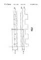
- the cards 1 having a contact-type operating modecomprise an integrated circuit chip 2 wherein at least five contact pads 100 , 101 , 102 , 103 and 104 are electrically connected, by conductive leads not 30 represented, respectively to five contact regions 200 , 201 , 202 , 203 and 204 located on the surface of the card body 3 .
- a contact pad Reset 100is connected to a contact region Reset 200 , a contact pad Clock 101 is connected to a contact region Clock 201 , a contact pad Iss 102 is connected to a contact region Vss 202 , a contact pad I/O 103 is connected to a contact region I/O 203 , and a contact pad Idd 104 is connected to a contact region Vdd 204 .
- a current respectively named I Reset , I Clock , I SS , I I/O and I ddis passing through respectively the contact pads 100 , 101 , 102 , 103 and 104 , as well as the contact regions 200 , 201 , 202 , 203 and 204 .
- the assembly of the chip 2 , the conductive leads and the contact regions 200 , 201 , 202 , 203 and 204is generally comprised in an electronic module 4 incorporated into the card body 3 .
- the integrated circuit device according to the inventioncan be the electronic module 4 carrying the regions 200 , 201 , 202 , 203 and 204 and comprising a chip, or the chip 2 itself.
- the integrated circuit devicecomprises a capacitor 8 .
- Its capacitance 8is characterized by a value greater than about 0.1 nanofarad, particularly on the order of 1 nanofarad.
- the incoming current Iddis filtered by a second order filter constituted by the resistance, if any, of connection circuit 120 in series with self-inductor 9 in series with capacitor 8 connected in parallel with the integrated circuit.
- Capacitor 8supplies rapid current charges to the integrated circuit while the self-inductor 9 opposes any rapid changes in Idd.
- this arrangementis capable of attenuating the amplitude of the peaks of the current consumed by the integrated circuit of the device according to the invention.
- the integrated circuit device according to the inventionadvantageously includes an electrical resistor. Its electrical resistance is characterized by a value greater than about 1 ohm, particularly on the order of 10 ohms. It is preferably constituted by a self-inductor 9 .
- the self-inductance 9is itself characterized by a value greater than about 50 nanohenries, particularly 500 nanohenries.
- the capacitor 8is electrically connected to the pad 102 of the chip 2 or to the region 202 of the electronic module comprising said chip 2 , and to the pad 104 of the chip 2 or to the pad 204 of the electronic module 4 .
- this self-inductor 9is electrically connected to the pad 104 of the chip 2 or to the region 204 of the electronic module 4 comprising said chip 2 and connected in series with the capacitor 8 .
- the capacitor 8 and self-inductor 9 assemblyconstitutes a low-pass filtering cell, this filtering cell being constituted by at least a capacitor 8 , preferably by a capacitor 8 and a resistor, the resistor preferably being a self-inductor 9 , said filtering cell being located in the electronic module 4 , advantageously in the immediate vicinity of the integrated circuit.
- the chip 2comprises the capacitor 8 and the self-inductor 9 .
- the chip 2comprises three main layers. These include a first base layer 105 , a supplementary layer 106 , said first and second layers being linked by an intermediate embedding layer 107 .
- the layer 105is composed of three sub-layers, a silicon sub-layer 108 , a circuit integrating sub-layer 109 , said sub-layers 108 and 109 being surmounted by a passivation layer 110 .
- the layer 106is composed of six sub-layers, an insulating sub-layer 111 , a conductive sub-layer 112 , for example tantalum-based, forming a first electrode of the capacitor 8 , an insulating and dielectric sub-layer 113 , for example of tantalum oxide, a conductive sub-layer 114 , for example tantalum-based, forming a second electrode of the capacitor 8 , an insulating sub-layer 115 and a layer 116 of silicon or another material.
- the embedding layer 107is not subdivided into sub-layers. It is composed of an embedding agent, for example a polymer. It could be, in particular, a polyimide.
- the thickness of the sub-layers 110 , 111 , 112 , 113 , 114 and 115is on the order of several thousand angstroms
- the thickness of the sub-layer 109 and the sub-layer 107is on the order of 5 ⁇ m
- the thickness of the sub-layer 108is on the order of 50 ⁇ m
- the thickness of the layer 116is on the order of 150 ⁇ m.
- the capacitor 8is thus integrated into the supplementary layer 106 .
- the sub-layers 112 and 114 forming electrodesare electrically connected to interconnection pads 117 , 118 of the integrated circuit by vias or conductive bumps 119 .
- the self-inductor 9is in the form of a coil integrated into the active side of the base layer 105 .
- One of its two connection terminalsis connected to the contact pad Idd 104 , and the other to the interconnection pad 118 .
- the interconnection pad 117is connected to the contact pad Vss 102 by a connection circuit 120 , which is advantageously has the least resistance possible.
- the layers 106 and 107are pierced with holes using micromachining techniques. These holes make it possible to establish connections by thermosonic wiring between the pads 100 , 101 , 102 , 103 and. 104 located on the active side of the base layer 105 and the contact pads 200 , 201 , 202 , 203 and 204 of the electronic module 4 .
- the integrated circuitforms a complex structure of assembled logic cells, in which a central processing unit (CPU) distributes and manages, through a data bus and an address bus, information stored in RAM, ROM or EEPROM memories of said circuit.
- the integrated circuitmay also form a microcontroller associated with the CPU, said microcontroller being more specifically intended for the cryptographic encoding of data requiring specialized calculation structures.
- This microcontrolleris also called a cryptoprocessor.
- FIG. 7represents an elementary logic cell 5 of an integrated circuit device according to the invention.
- This cell 5is of the CMOS type. It is constituted by a first MOS transistor 6 of the P type and a second MOS transistor 7 of the N type, said transistors 6 , 7 being connected in series.
- Each cell 5is controlled by a logical control signal Vin common to both transistors 6 , 7 .
- iddbe the intensity of the current consumed by the cell 5 .
- a curve 300represents the intensity of the current Idd consumed in an integrated circuit device according to the invention as a function of time
- a curve 301represents the intensity of the current Idd consumed in a device according to the prior art as a function of time
- the curves 300 and 301being compared to a curve 302 representing the clock signal that controls this integrated circuit device.
- the integrated circuit devices according to the invention and according to the prior artwhich respectively produce the curves 300 and 301 , consume power both on the rising edge and on the falling edge of the clock. It will be noted however, that this is not always the case. In fact, certain integrated circuit devices consume power on only one of the two clock edges fronts, and others have frequency multiplying means, in which case the number of current peaks per clock period is greater than two.
- the curve 301shows peaks in the intensity of the current Idd consumed whose height or amplitude is on the order of 27 mA. These peaks constitute a signature of the set of tasks performed by the integrated circuit.
- the curve 300shows peaks in the intensity of the current Idd consumed whose height is on the order of 8 mA.
- the height of the peakshas been reduced by more than 50%.
- the careful analysis of the curve 300 in association with a transactionis thus especially complex. It is no longer possible to simply extract the confidential information using a non-destructive investigation method.
- CMOS integrated circuitsare such that an integrated circuit device can be powered, in a degraded way, by its contact pads Reset 100 , I/O 103 or Clock 101 .
- These padsunlike the supply pads Vss and Vdd are protected from electrostatic discharges, by non-linear devices. These devices are primarily constituted by two diodes connected to the supply bus of the integrated circuit. Thus, any supplying of power to the integrated circuits, in the degraded mode, by the pads Reset, I/O and Clock takes place through a diode to the power supply Vdd.
- This non-linear deviceassociated with the capacitor present in the Vdd, filters the supply current of the integrated circuit.
- the embodiment described in the present specification with respect to the pads Vss and Vddcan be applied to the pads 100 , 101 or 103 in order to attenuate the signatures of the electrical consumption of the integrated circuit in these pads.
- the integrated circuit chips according to the inventioncan be produced in batches, in the form of silicon slices known as wafers.
- wafersFor information on the batch production of chips, the reader is referred to the patent application filed in France under the number 97/10764, which has not yet been published, whose content is incorporated into the present application by reference.
- the present inventioncan increase the efficiency of programming routines by filtering, by means of an analog cell, the transient current phenomena that accompany all the tasks of an integrated circuit for a chip card.
Landscapes
- Engineering & Computer Science (AREA)
- Computer Hardware Design (AREA)
- Microelectronics & Electronic Packaging (AREA)
- Physics & Mathematics (AREA)
- General Physics & Mathematics (AREA)
- Theoretical Computer Science (AREA)
- Computer Security & Cryptography (AREA)
- General Engineering & Computer Science (AREA)
- Semiconductor Integrated Circuits (AREA)
- Storage Device Security (AREA)
- Credit Cards Or The Like (AREA)
Abstract
Description
Claims (19)
Applications Claiming Priority (3)
| Application Number | Priority Date | Filing Date | Title |
|---|---|---|---|
| FR9801305AFR2774492A1 (en) | 1998-02-04 | 1998-02-04 | DEVICE WITH INTEGRATED CIRCUIT SECURED BY MITIGATION OF ELECTRIC SIGNATURES |
| FR9801305 | 1998-02-04 | ||
| PCT/FR1999/000246WO1999040538A1 (en) | 1998-02-04 | 1999-02-04 | Device with integrated circuit made secure by attenuation of electric signatures |
Publications (1)
| Publication Number | Publication Date |
|---|---|
| US6695214B1true US6695214B1 (en) | 2004-02-24 |
Family
ID=9522595
Family Applications (1)
| Application Number | Title | Priority Date | Filing Date |
|---|---|---|---|
| US09/601,656Expired - LifetimeUS6695214B1 (en) | 1998-02-04 | 1999-02-04 | Device with integrated circuit made secure by attenuation of electric signatures |
Country Status (7)
| Country | Link |
|---|---|
| US (1) | US6695214B1 (en) |
| EP (1) | EP1053531B2 (en) |
| JP (2) | JP2002503006A (en) |
| CN (1) | CN1162805C (en) |
| DE (1) | DE69900463T2 (en) |
| FR (1) | FR2774492A1 (en) |
| WO (1) | WO1999040538A1 (en) |
Cited By (4)
| Publication number | Priority date | Publication date | Assignee | Title |
|---|---|---|---|---|
| US20060041402A1 (en)* | 2003-01-14 | 2006-02-23 | Koninklijke Philips Electronics N.V. | Method and terminal for detecting fake and/or modified smart card |
| US20080040593A1 (en)* | 2006-08-11 | 2008-02-14 | Atmel Corporation | Embedded software camouflage against code reverse engineering |
| US20080040607A1 (en)* | 2006-08-10 | 2008-02-14 | Majid Kaabouch | Software execution randomization |
| US20080123446A1 (en)* | 2006-09-21 | 2008-05-29 | Stephen Charles Pickles | Randomizing Current Consumption in Memory Devices |
Families Citing this family (6)
| Publication number | Priority date | Publication date | Assignee | Title |
|---|---|---|---|---|
| DE69937629T2 (en)* | 1998-07-07 | 2008-11-13 | Nxp B.V. | DATA CARRIER EQUIPPED WITH DATA PROCESSING OPTIONS AND CURRENT TOP STYLE SUPPRESSION POSSIBILITIES |
| FR2800490B1 (en)* | 1999-11-02 | 2002-01-04 | Sagem | METHOD FOR ENSURING THE INVIOLABILITY OF A SMART CARD MICROMODULE AGAINST AN ANALYSIS OF ITS CURRENT CONSUMPTION AND MICROMODULE AGENCY FOR ITS IMPLEMENTATION |
| FR2801746B1 (en) | 1999-11-26 | 2003-08-22 | France Telecom | DEVICE FOR STABILIZED POWER SUPPLY OF ELECTRONIC TELE-FOOD COMPONENTS |
| US6507913B1 (en) | 1999-12-30 | 2003-01-14 | Yeda Research And Development Co. Ltd. | Protecting smart cards from power analysis with detachable power supplies |
| FR2811790A1 (en)* | 2000-07-11 | 2002-01-18 | Schlumberger Systems & Service | Smart card microcontroller secured against current attacks, uses module between processor and external supply which chaotically encrypts supply current fluctuations |
| DE10054970A1 (en) | 2000-11-06 | 2002-05-23 | Infineon Technologies Ag | Method for controlling the charging and discharging phases of a backup capacitor |
Citations (9)
| Publication number | Priority date | Publication date | Assignee | Title |
|---|---|---|---|---|
| US4810864A (en)* | 1986-11-07 | 1989-03-07 | Seiko Instruments Inc. | Memory card having improved data protection |
| US4864292A (en) | 1986-11-14 | 1989-09-05 | Nederlandse Organisatie Voor Toegepast-Natuurwetenschappelijk Onderzoek Tno | Identification system |
| US5687109A (en)* | 1988-05-31 | 1997-11-11 | Micron Technology, Inc. | Integrated circuit module having on-chip surge capacitors |
| US5745336A (en)* | 1991-12-25 | 1998-04-28 | Hitachi, Ltd. | Capacitor for semiconductor integrated circuit |
| US5847447A (en)* | 1996-07-09 | 1998-12-08 | Ambient Corporation | Capcitively coupled bi-directional data and power transmission system |
| US5986890A (en)* | 1995-12-22 | 1999-11-16 | Giesecke & Devrient Gmbh | Semifinished product with an electronic module |
| US6147857A (en)* | 1997-10-07 | 2000-11-14 | E. R. W. | Optional on chip power supply bypass capacitor |
| JP2001000664A (en)* | 1999-06-21 | 2001-01-09 | Ai Narushisu Kk | Pachinko game machine |
| US6276609B1 (en)* | 1998-07-07 | 2001-08-21 | U.S. Philips Corporation | Data carrier provided data processing means and current peak pattern suppression means |
Family Cites Families (13)
| Publication number | Priority date | Publication date | Assignee | Title |
|---|---|---|---|---|
| JPS63270194A (en)* | 1987-04-30 | 1988-11-08 | 株式会社東芝 | portable storage medium |
| DE3903454A1 (en)† | 1988-12-12 | 1990-06-13 | Raymund H Eisele | ELEMENT INSERTABLE IN IT FACILITIES |
| JPH04116783A (en)* | 1990-09-06 | 1992-04-17 | Mitsubishi Electric Corp | Power supply circuit device for ic card and ic card |
| JPH04186667A (en)* | 1990-11-16 | 1992-07-03 | Omron Corp | Semiconductor device |
| DE4230148C2 (en)† | 1992-09-09 | 1994-08-25 | Angewandte Digital Elektronik | Circuit arrangement for detecting an interruption in the electrical connection of contactless chip cards to their read / write device |
| DE4301039C2 (en)† | 1993-01-16 | 1995-06-14 | Uwe Dipl Ing Latsch | Electronic system for managing shared motor vehicles |
| DE9421565U1 (en)† | 1994-12-24 | 1996-02-29 | Orga Kartensysteme GmbH, 33104 Paderborn | Fee collection system for road use of vehicles |
| JP3820600B2 (en)* | 1994-12-28 | 2006-09-13 | ソニー株式会社 | IC card and semiconductor integrated circuit |
| DE19503607A1 (en)† | 1995-02-03 | 1996-08-08 | Angewandte Digital Elektronik | Chip cards for displaying different card information |
| DE19536169A1 (en)† | 1995-09-29 | 1997-04-03 | Ibm | Multifunctional chip card |
| JP3755675B2 (en)† | 1995-11-20 | 2006-03-15 | ソニー株式会社 | Clamp circuit, CMOS chip IC and contactless information card |
| DE29602609U1 (en)† | 1996-02-15 | 1997-06-12 | Robert Bosch Gmbh, 70469 Stuttgart | Advanced electronic smart card facility |
| JPH10193849A (en)† | 1996-12-27 | 1998-07-28 | Rohm Co Ltd | Circuit chip-mounted card and circuit chip module |
- 1998
- 1998-02-04FRFR9801305Apatent/FR2774492A1/ennot_activeWithdrawn
- 1999
- 1999-02-04CNCNB998025623Apatent/CN1162805C/ennot_activeExpired - Fee Related
- 1999-02-04WOPCT/FR1999/000246patent/WO1999040538A1/enactiveIP Right Grant
- 1999-02-04JPJP2000530881Apatent/JP2002503006A/ennot_activeWithdrawn
- 1999-02-04EPEP99902596Apatent/EP1053531B2/ennot_activeExpired - Lifetime
- 1999-02-04USUS09/601,656patent/US6695214B1/ennot_activeExpired - Lifetime
- 1999-02-04DEDE69900463Tpatent/DE69900463T2/ennot_activeExpired - Lifetime
- 2010
- 2010-10-12JPJP2010229577Apatent/JP2011060303A/enactivePending
Patent Citations (9)
| Publication number | Priority date | Publication date | Assignee | Title |
|---|---|---|---|---|
| US4810864A (en)* | 1986-11-07 | 1989-03-07 | Seiko Instruments Inc. | Memory card having improved data protection |
| US4864292A (en) | 1986-11-14 | 1989-09-05 | Nederlandse Organisatie Voor Toegepast-Natuurwetenschappelijk Onderzoek Tno | Identification system |
| US5687109A (en)* | 1988-05-31 | 1997-11-11 | Micron Technology, Inc. | Integrated circuit module having on-chip surge capacitors |
| US5745336A (en)* | 1991-12-25 | 1998-04-28 | Hitachi, Ltd. | Capacitor for semiconductor integrated circuit |
| US5986890A (en)* | 1995-12-22 | 1999-11-16 | Giesecke & Devrient Gmbh | Semifinished product with an electronic module |
| US5847447A (en)* | 1996-07-09 | 1998-12-08 | Ambient Corporation | Capcitively coupled bi-directional data and power transmission system |
| US6147857A (en)* | 1997-10-07 | 2000-11-14 | E. R. W. | Optional on chip power supply bypass capacitor |
| US6276609B1 (en)* | 1998-07-07 | 2001-08-21 | U.S. Philips Corporation | Data carrier provided data processing means and current peak pattern suppression means |
| JP2001000664A (en)* | 1999-06-21 | 2001-01-09 | Ai Narushisu Kk | Pachinko game machine |
Cited By (10)
| Publication number | Priority date | Publication date | Assignee | Title |
|---|---|---|---|---|
| US20060041402A1 (en)* | 2003-01-14 | 2006-02-23 | Koninklijke Philips Electronics N.V. | Method and terminal for detecting fake and/or modified smart card |
| US7454318B2 (en)* | 2003-01-14 | 2008-11-18 | Nxp B.V. | Method and terminal for detecting fake and/or modified smart card |
| US20080040607A1 (en)* | 2006-08-10 | 2008-02-14 | Majid Kaabouch | Software execution randomization |
| US8301890B2 (en) | 2006-08-10 | 2012-10-30 | Inside Secure | Software execution randomization |
| US20080040593A1 (en)* | 2006-08-11 | 2008-02-14 | Atmel Corporation | Embedded software camouflage against code reverse engineering |
| US7613907B2 (en) | 2006-08-11 | 2009-11-03 | Atmel Corporation | Embedded software camouflage against code reverse engineering |
| US20080123446A1 (en)* | 2006-09-21 | 2008-05-29 | Stephen Charles Pickles | Randomizing Current Consumption in Memory Devices |
| US7554865B2 (en) | 2006-09-21 | 2009-06-30 | Atmel Corporation | Randomizing current consumption in memory devices |
| US20090257295A1 (en)* | 2006-09-21 | 2009-10-15 | Atmel Corporation | Randomizing Current Consumption in Memory Devices |
| US8031540B2 (en) | 2006-09-21 | 2011-10-04 | Atmel Corporation | Randomizing current consumption in memory devices |
Also Published As
| Publication number | Publication date |
|---|---|
| DE69900463D1 (en) | 2001-12-20 |
| JP2002503006A (en) | 2002-01-29 |
| JP2011060303A (en) | 2011-03-24 |
| EP1053531A1 (en) | 2000-11-22 |
| EP1053531B2 (en) | 2010-09-29 |
| EP1053531B1 (en) | 2001-11-14 |
| CN1162805C (en) | 2004-08-18 |
| CN1289427A (en) | 2001-03-28 |
| FR2774492A1 (en) | 1999-07-30 |
| DE69900463T2 (en) | 2002-09-05 |
| WO1999040538A1 (en) | 1999-08-12 |
Similar Documents
| Publication | Publication Date | Title |
|---|---|---|
| JP2011060303A (en) | Device with integrated circuit made secure by attenuation of electronic signatures | |
| KR100827218B1 (en) | Fingerprint based smart card | |
| JP2632703B2 (en) | Apparatus for detecting and removing passivation layer of integrated circuit | |
| US6802008B1 (en) | IC card and IC chip module | |
| US7923830B2 (en) | Package-on-package secure module having anti-tamper mesh in the substrate of the upper package | |
| RU2285291C2 (en) | Chip-card with display | |
| JP4769398B2 (en) | Microcontroller protected against current attack | |
| US5981971A (en) | Semiconductor ROM wafer test structure, and IC card | |
| US20080164324A1 (en) | Input/output pads placement for a smart card chip | |
| JP2000515669A (en) | Semiconductor memory for secure data storage | |
| JP3641182B2 (en) | Self-destructive semiconductor device | |
| JPH03142296A (en) | Data carrier | |
| US20060108416A1 (en) | Unauthorized access prevention method | |
| JP3641149B2 (en) | Self-destructive semiconductor device | |
| US6276609B1 (en) | Data carrier provided data processing means and current peak pattern suppression means | |
| JP2003529986A (en) | Output stage for communication contacts for data carriers | |
| EP0890956A2 (en) | Semiconductor device having a security circuit for preventing illegal access | |
| Shigematsu et al. | A 15/spl times/15 mm/sup 2/single-chip fingerprint sensor and identifier using pixel-parallel processing | |
| JPS6142085A (en) | IC card | |
| JPS5922354A (en) | IC card | |
| JPS63270194A (en) | portable storage medium | |
| JPH0241292A (en) | IC card | |
| JPS63110768A (en) | semiconductor equipment | |
| HK1019953A (en) | Semiconductor memory for secure data storage |
Legal Events
| Date | Code | Title | Description |
|---|---|---|---|
| AS | Assignment | Owner name:SCHLUMBERGER SYSTEMES, FRANCE Free format text:ASSIGNMENT OF ASSIGNORS INTEREST;ASSIGNOR:LEYDIER, ROBERT;REEL/FRAME:011349/0436 Effective date:20001110 Owner name:SCHLUMBERGER SYSTEMES, FRANCE Free format text:ASSIGNMENT OF ASSIGNORS INTEREST;ASSIGNOR:SERVEL, ERIC;REEL/FRAME:011349/0527 Effective date:20001113 Owner name:SCHLUMBERGER SYSTEMES, FRANCE Free format text:ASSIGNMENT OF ASSIGNORS INTEREST;ASSIGNOR:BONVALOT, BEATRICE;REEL/FRAME:011350/0457 Effective date:20001106 | |
| STCF | Information on status: patent grant | Free format text:PATENTED CASE | |
| AS | Assignment | Owner name:AXALTO S.A., FRANCE Free format text:CHANGE OF NAME;ASSIGNOR:SCHLUMBERGER SYSTEMES;REEL/FRAME:017145/0242 Effective date:20040311 | |
| FPAY | Fee payment | Year of fee payment:4 | |
| AS | Assignment | Owner name:GEMALTO SA, FRANCE Free format text:CHANGE OF NAME;ASSIGNOR:AXALTO SA;REEL/FRAME:022127/0852 Effective date:20060905 | |
| FPAY | Fee payment | Year of fee payment:8 | |
| FPAY | Fee payment | Year of fee payment:12 |