US6693934B2 - Wavelength division multiplexed vertical cavity surface emitting laser array - Google Patents
Wavelength division multiplexed vertical cavity surface emitting laser arrayDownload PDFInfo
- Publication number
- US6693934B2 US6693934B2US10/028,438US2843801AUS6693934B2US 6693934 B2US6693934 B2US 6693934B2US 2843801 AUS2843801 AUS 2843801AUS 6693934 B2US6693934 B2US 6693934B2
- Authority
- US
- United States
- Prior art keywords
- spacer
- fabricating
- active region
- surface emitting
- emitting laser
- Prior art date
- Legal status (The legal status is an assumption and is not a legal conclusion. Google has not performed a legal analysis and makes no representation as to the accuracy of the status listed.)
- Expired - Fee Related
Links
- 125000006850spacer groupChemical group0.000claimsabstractdescription84
- 230000008021depositionEffects0.000claimsabstractdescription13
- 238000005530etchingMethods0.000claimsabstractdescription12
- 239000000463materialSubstances0.000claimsdescription27
- 238000004519manufacturing processMethods0.000claimsdescription26
- 239000000758substrateSubstances0.000claimsdescription23
- VYPSYNLAJGMNEJ-UHFFFAOYSA-NSilicium dioxideChemical compoundO=[Si]=OVYPSYNLAJGMNEJ-UHFFFAOYSA-N0.000claimsdescription10
- 238000002955isolationMethods0.000claimsdescription7
- 229910052681coesiteInorganic materials0.000claimsdescription5
- 229910052906cristobaliteInorganic materials0.000claimsdescription5
- 239000011521glassSubstances0.000claimsdescription5
- 239000000377silicon dioxideSubstances0.000claimsdescription5
- 229910052682stishoviteInorganic materials0.000claimsdescription5
- 229910052905tridymiteInorganic materials0.000claimsdescription5
- 230000001419dependent effectEffects0.000claimsdescription2
- 238000003491arrayMethods0.000abstractdescription14
- 230000012010growthEffects0.000abstractdescription3
- 238000000034methodMethods0.000description19
- 238000000151depositionMethods0.000description10
- 238000000926separation methodMethods0.000description7
- 230000009286beneficial effectEffects0.000description6
- 230000003287optical effectEffects0.000description6
- JBRZTFJDHDCESZ-UHFFFAOYSA-NAsGaChemical compound[As]#[Ga]JBRZTFJDHDCESZ-UHFFFAOYSA-N0.000description4
- 238000012986modificationMethods0.000description4
- 230000004048modificationEffects0.000description4
- 229910001218Gallium arsenideInorganic materials0.000description3
- 238000000623plasma-assisted chemical vapour depositionMethods0.000description2
- 239000004065semiconductorSubstances0.000description2
- 238000000137annealingMethods0.000description1
- 238000005229chemical vapour depositionMethods0.000description1
- 238000013500data storageMethods0.000description1
- 238000001451molecular beam epitaxyMethods0.000description1
- 230000003647oxidationEffects0.000description1
- 238000007254oxidation reactionMethods0.000description1
Images


Classifications
- H—ELECTRICITY
- H01—ELECTRIC ELEMENTS
- H01S—DEVICES USING THE PROCESS OF LIGHT AMPLIFICATION BY STIMULATED EMISSION OF RADIATION [LASER] TO AMPLIFY OR GENERATE LIGHT; DEVICES USING STIMULATED EMISSION OF ELECTROMAGNETIC RADIATION IN WAVE RANGES OTHER THAN OPTICAL
- H01S5/00—Semiconductor lasers
- H01S5/40—Arrangement of two or more semiconductor lasers, not provided for in groups H01S5/02 - H01S5/30
- H01S5/42—Arrays of surface emitting lasers
- H01S5/423—Arrays of surface emitting lasers having a vertical cavity
- H—ELECTRICITY
- H01—ELECTRIC ELEMENTS
- H01S—DEVICES USING THE PROCESS OF LIGHT AMPLIFICATION BY STIMULATED EMISSION OF RADIATION [LASER] TO AMPLIFY OR GENERATE LIGHT; DEVICES USING STIMULATED EMISSION OF ELECTROMAGNETIC RADIATION IN WAVE RANGES OTHER THAN OPTICAL
- H01S2304/00—Special growth methods for semiconductor lasers
- H01S2304/02—MBE
- H—ELECTRICITY
- H01—ELECTRIC ELEMENTS
- H01S—DEVICES USING THE PROCESS OF LIGHT AMPLIFICATION BY STIMULATED EMISSION OF RADIATION [LASER] TO AMPLIFY OR GENERATE LIGHT; DEVICES USING STIMULATED EMISSION OF ELECTROMAGNETIC RADIATION IN WAVE RANGES OTHER THAN OPTICAL
- H01S5/00—Semiconductor lasers
- H01S5/10—Construction or shape of the optical resonator, e.g. extended or external cavity, coupled cavities, bent-guide, varying width, thickness or composition of the active region
- H01S5/18—Surface-emitting [SE] lasers, e.g. having both horizontal and vertical cavities
- H01S5/183—Surface-emitting [SE] lasers, e.g. having both horizontal and vertical cavities having only vertical cavities, e.g. vertical cavity surface-emitting lasers [VCSEL]
- H01S5/18358—Surface-emitting [SE] lasers, e.g. having both horizontal and vertical cavities having only vertical cavities, e.g. vertical cavity surface-emitting lasers [VCSEL] containing spacer layers to adjust the phase of the light wave in the cavity
- H—ELECTRICITY
- H01—ELECTRIC ELEMENTS
- H01S—DEVICES USING THE PROCESS OF LIGHT AMPLIFICATION BY STIMULATED EMISSION OF RADIATION [LASER] TO AMPLIFY OR GENERATE LIGHT; DEVICES USING STIMULATED EMISSION OF ELECTROMAGNETIC RADIATION IN WAVE RANGES OTHER THAN OPTICAL
- H01S5/00—Semiconductor lasers
- H01S5/40—Arrangement of two or more semiconductor lasers, not provided for in groups H01S5/02 - H01S5/30
- H01S5/4025—Array arrangements, e.g. constituted by discrete laser diodes or laser bar
- H01S5/4087—Array arrangements, e.g. constituted by discrete laser diodes or laser bar emitting more than one wavelength
Definitions
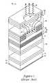
- DBRs 316that are spaced apart from each other, with the separation between each of the DBRs 316 being an integer multiple of L.
- Electrical contacts(which are not shown, but reference the contacts 550 in FIG. 5) for the individual VCSEL elements are then provided.
- Isolation regions 455are also formed in suitable locations including a location between the top DBRs 316 .
Landscapes
- Physics & Mathematics (AREA)
- Condensed Matter Physics & Semiconductors (AREA)
- General Physics & Mathematics (AREA)
- Electromagnetism (AREA)
- Optics & Photonics (AREA)
- Semiconductor Lasers (AREA)
Abstract
Description
Claims (29)
Priority Applications (4)
| Application Number | Priority Date | Filing Date | Title |
|---|---|---|---|
| US10/028,438US6693934B2 (en) | 2001-12-28 | 2001-12-28 | Wavelength division multiplexed vertical cavity surface emitting laser array |
| CA002472061ACA2472061A1 (en) | 2001-12-28 | 2002-12-13 | Wavelength division multiplexed vertical cavity surface emitting laser array |
| PCT/US2002/041735WO2003058775A2 (en) | 2001-12-28 | 2002-12-13 | Wavelength division multiplexed vertical cavity surface emitting laser array |
| EP02796120AEP1461851A2 (en) | 2001-12-28 | 2002-12-13 | Multiple wavelength vertical cavity surface emitting laser array |
Applications Claiming Priority (1)
| Application Number | Priority Date | Filing Date | Title |
|---|---|---|---|
| US10/028,438US6693934B2 (en) | 2001-12-28 | 2001-12-28 | Wavelength division multiplexed vertical cavity surface emitting laser array |
Publications (2)
| Publication Number | Publication Date |
|---|---|
| US20030123507A1 US20030123507A1 (en) | 2003-07-03 |
| US6693934B2true US6693934B2 (en) | 2004-02-17 |
Family
ID=21843445
Family Applications (1)
| Application Number | Title | Priority Date | Filing Date |
|---|---|---|---|
| US10/028,438Expired - Fee RelatedUS6693934B2 (en) | 2001-12-28 | 2001-12-28 | Wavelength division multiplexed vertical cavity surface emitting laser array |
Country Status (4)
| Country | Link |
|---|---|
| US (1) | US6693934B2 (en) |
| EP (1) | EP1461851A2 (en) |
| CA (1) | CA2472061A1 (en) |
| WO (1) | WO2003058775A2 (en) |
Cited By (9)
| Publication number | Priority date | Publication date | Assignee | Title |
|---|---|---|---|---|
| US20040076198A1 (en)* | 2002-10-16 | 2004-04-22 | Spoonhower John P. | Tunable organic VCSEL system |
| US20050030540A1 (en)* | 2003-04-11 | 2005-02-10 | Thornton Robert L. | Optical spectroscopy apparatus and method for measurement of analyte concentrations or other such species in a specimen employing a semiconductor laser-pumped, small-cavity fiber laser |
| US20060022266A1 (en)* | 2004-07-30 | 2006-02-02 | International Business Machines Corporation | Manufacturable recessed strained rsd structure and process for advanced cmos |
| US20060045158A1 (en)* | 2004-08-30 | 2006-03-02 | Chian Chiu Li | Stack-type Wavelength-tunable Laser Source |
| US20070063140A1 (en)* | 2005-09-22 | 2007-03-22 | Honeywell International Inc. | Optical particulate sensor in oil quality detection |
| KR100734565B1 (en) | 2005-08-19 | 2007-07-03 | 광주과학기술원 | Manufacturing method of RCC-PD |
| US20080086038A1 (en)* | 2003-04-11 | 2008-04-10 | Thornton Robert L | Method for measurement of analyte concentrations and a semiconductor laser-pumped, small-cavity fiber lasers for such measurements and other applications |
| US9065587B2 (en) | 2010-10-08 | 2015-06-23 | Hewlett-Packard Development Company, L.P. | Optical multiplexing using laser arrays |
| US9160481B2 (en) | 2010-10-08 | 2015-10-13 | Hewlett-Packard Development Company, L.P. | Optical polarization multiplexing using laser arrays |
Families Citing this family (3)
| Publication number | Priority date | Publication date | Assignee | Title |
|---|---|---|---|---|
| US20070041416A1 (en)* | 2005-08-19 | 2007-02-22 | Koelle Bernhard U | Tunable long-wavelength VCSEL system |
| WO2016195695A1 (en)* | 2015-06-04 | 2016-12-08 | Hewlett Packard Enterprise Development Lp | Monolithic wdm vcsels with spatially varying gain peak and fabry perot wavelength |
| CN116417897A (en)* | 2021-12-31 | 2023-07-11 | 浙江睿熙科技有限公司 | VCSEL chip and preparation method thereof |
Citations (8)
| Publication number | Priority date | Publication date | Assignee | Title |
|---|---|---|---|---|
| US5388120A (en)* | 1993-09-21 | 1995-02-07 | Motorola, Inc. | VCSEL with unstable resonator |
| US5699375A (en)* | 1996-07-08 | 1997-12-16 | Xerox Corporation | Multiple wavelength, surface emitting laser with broad bandwidth distributed Bragg reflectors |
| US6195485B1 (en) | 1998-10-26 | 2001-02-27 | The Regents Of The University Of California | Direct-coupled multimode WDM optical data links with monolithically-integrated multiple-channel VCSEL and photodetector |
| US6362069B1 (en)* | 2000-12-28 | 2002-03-26 | The Trustees Of Princeton University | Long-wavelength VCSELs and method of manufacturing same |
| US20020080836A1 (en)* | 2000-12-23 | 2002-06-27 | Applied Optoelectronics, Inc. | Vertical-cavity surface-emitting laser with metal mirror and method of fabrication of same |
| US20020106160A1 (en)* | 2000-12-29 | 2002-08-08 | Honeywell International Inc. | Resonant reflector for increased wavelength and polarization control |
| US20030021317A1 (en)* | 2001-07-25 | 2003-01-30 | Liao Andrew Shuh-Huei | Vertical cavity surface emitting laser having improved light output function |
| US20030034508A1 (en)* | 2001-08-16 | 2003-02-20 | Motorola, Inc. | Microprocessor in MOS with integrated cordic in compound semiconductor on a common substrate |
Family Cites Families (2)
| Publication number | Priority date | Publication date | Assignee | Title |
|---|---|---|---|---|
| US5898722A (en)* | 1997-03-10 | 1999-04-27 | Motorola, Inc. | Dual wavelength monolithically integrated vertical cavity surface emitting lasers and method of fabrication |
| US6117699A (en)* | 1998-04-10 | 2000-09-12 | Hewlett-Packard Company | Monolithic multiple wavelength VCSEL array |
- 2001
- 2001-12-28USUS10/028,438patent/US6693934B2/ennot_activeExpired - Fee Related
- 2002
- 2002-12-13WOPCT/US2002/041735patent/WO2003058775A2/ennot_activeApplication Discontinuation
- 2002-12-13CACA002472061Apatent/CA2472061A1/ennot_activeAbandoned
- 2002-12-13EPEP02796120Apatent/EP1461851A2/ennot_activeWithdrawn
Patent Citations (8)
| Publication number | Priority date | Publication date | Assignee | Title |
|---|---|---|---|---|
| US5388120A (en)* | 1993-09-21 | 1995-02-07 | Motorola, Inc. | VCSEL with unstable resonator |
| US5699375A (en)* | 1996-07-08 | 1997-12-16 | Xerox Corporation | Multiple wavelength, surface emitting laser with broad bandwidth distributed Bragg reflectors |
| US6195485B1 (en) | 1998-10-26 | 2001-02-27 | The Regents Of The University Of California | Direct-coupled multimode WDM optical data links with monolithically-integrated multiple-channel VCSEL and photodetector |
| US20020080836A1 (en)* | 2000-12-23 | 2002-06-27 | Applied Optoelectronics, Inc. | Vertical-cavity surface-emitting laser with metal mirror and method of fabrication of same |
| US6362069B1 (en)* | 2000-12-28 | 2002-03-26 | The Trustees Of Princeton University | Long-wavelength VCSELs and method of manufacturing same |
| US20020106160A1 (en)* | 2000-12-29 | 2002-08-08 | Honeywell International Inc. | Resonant reflector for increased wavelength and polarization control |
| US20030021317A1 (en)* | 2001-07-25 | 2003-01-30 | Liao Andrew Shuh-Huei | Vertical cavity surface emitting laser having improved light output function |
| US20030034508A1 (en)* | 2001-08-16 | 2003-02-20 | Motorola, Inc. | Microprocessor in MOS with integrated cordic in compound semiconductor on a common substrate |
Non-Patent Citations (2)
| Title |
|---|
| S.Y. Hu, et al., "Multiple-Wavelength Top-emitting Vertical Cavity Photonic Integrated Emitter Arrays for Direct-Coupled Wavelength Division Multiplexing Applications", Electronics Letters, vol. 34, No. 2, Jan. 1998. |
| S.Y. Hu, et al., "Optical Crosstalk in Monolithically Integrated Multiple-Wavelength Vertical Cavity Surface Laser Arrays for Multimode WDM Local-Area Networks", Electronics Letters, vol. 34, No. 7, Apr. 1998. |
Cited By (16)
| Publication number | Priority date | Publication date | Assignee | Title |
|---|---|---|---|---|
| US6970488B2 (en)* | 2002-10-16 | 2005-11-29 | Eastman Kodak Company | Tunable organic VCSEL system |
| US20040076198A1 (en)* | 2002-10-16 | 2004-04-22 | Spoonhower John P. | Tunable organic VCSEL system |
| US20080086038A1 (en)* | 2003-04-11 | 2008-04-10 | Thornton Robert L | Method for measurement of analyte concentrations and a semiconductor laser-pumped, small-cavity fiber lasers for such measurements and other applications |
| US20050030540A1 (en)* | 2003-04-11 | 2005-02-10 | Thornton Robert L. | Optical spectroscopy apparatus and method for measurement of analyte concentrations or other such species in a specimen employing a semiconductor laser-pumped, small-cavity fiber laser |
| US7633621B2 (en) | 2003-04-11 | 2009-12-15 | Thornton Robert L | Method for measurement of analyte concentrations and semiconductor laser-pumped, small-cavity fiber lasers for such measurements and other applications |
| US7283242B2 (en) | 2003-04-11 | 2007-10-16 | Thornton Robert L | Optical spectroscopy apparatus and method for measurement of analyte concentrations or other such species in a specimen employing a semiconductor laser-pumped, small-cavity fiber laser |
| US20060022266A1 (en)* | 2004-07-30 | 2006-02-02 | International Business Machines Corporation | Manufacturable recessed strained rsd structure and process for advanced cmos |
| US20060205189A1 (en)* | 2004-07-30 | 2006-09-14 | International Business Machines Corporation | Manufacturable recessed strained RSD structure and process for advanced CMOS |
| US7115955B2 (en)* | 2004-07-30 | 2006-10-03 | International Business Machines Corporation | Semiconductor device having a strained raised source/drain |
| US7446005B2 (en) | 2004-07-30 | 2008-11-04 | International Business Machines Corporation | Manufacturable recessed strained RSD structure and process for advanced CMOS |
| US20060045158A1 (en)* | 2004-08-30 | 2006-03-02 | Chian Chiu Li | Stack-type Wavelength-tunable Laser Source |
| KR100734565B1 (en) | 2005-08-19 | 2007-07-03 | 광주과학기술원 | Manufacturing method of RCC-PD |
| US7321117B2 (en) | 2005-09-22 | 2008-01-22 | Honeywell International Inc. | Optical particulate sensor in oil quality detection |
| US20070063140A1 (en)* | 2005-09-22 | 2007-03-22 | Honeywell International Inc. | Optical particulate sensor in oil quality detection |
| US9065587B2 (en) | 2010-10-08 | 2015-06-23 | Hewlett-Packard Development Company, L.P. | Optical multiplexing using laser arrays |
| US9160481B2 (en) | 2010-10-08 | 2015-10-13 | Hewlett-Packard Development Company, L.P. | Optical polarization multiplexing using laser arrays |
Also Published As
| Publication number | Publication date |
|---|---|
| US20030123507A1 (en) | 2003-07-03 |
| WO2003058775A3 (en) | 2004-03-18 |
| WO2003058775A2 (en) | 2003-07-17 |
| CA2472061A1 (en) | 2003-07-17 |
| EP1461851A2 (en) | 2004-09-29 |
Similar Documents
| Publication | Publication Date | Title |
|---|---|---|
| EP0858137B1 (en) | Surface emitting laser device and its method of manufacture | |
| JP3805522B2 (en) | Long wavelength emitting vertical cavity surface emitting laser and method of manufacturing the same | |
| US5062115A (en) | High density, independently addressable, surface emitting semiconductor laser/light emitting diode arrays | |
| US6560262B1 (en) | Vertical cavity surface emitting laser array and a process for making same | |
| EP1182758B1 (en) | Multi-wavelength surface emitting laser and method for manufacturing the same | |
| CN101443915A (en) | Quantum dot based optoelectronic device and method of making same | |
| JPH06224518A (en) | Monolithtic semiconductor device for generating surface skimming laser | |
| US6693934B2 (en) | Wavelength division multiplexed vertical cavity surface emitting laser array | |
| US12237648B2 (en) | Bi-directional vertical cavity surface emitting lasers | |
| US6798806B1 (en) | Hybrid mirror VCSELs | |
| US7095771B2 (en) | Implant damaged oxide insulating region in vertical cavity surface emitting laser | |
| US6738409B2 (en) | Current confinement, capacitance reduction and isolation of VCSELs using deep elemental traps | |
| US7170916B2 (en) | Selectively etchable heterogeneous composite distributed Bragg reflector | |
| US6594296B1 (en) | Surface-emitting laser and method of fabrication thereof | |
| US6621844B1 (en) | Buried oxide photonic device with large contact and precise aperture | |
| EP1564855B1 (en) | Surface emitting laser devices and method of manufacture | |
| KR102097687B1 (en) | Monolithic integrated transceiver device of a photodiode and a surface emitting laser and the fabrication method of this device | |
| WO1998048492A1 (en) | Electronic devices formed from pre-patterned structures that are bonded | |
| CN119256459A (en) | Two-dimensional matrix addressable VCSEL array | |
| CN119542917A (en) | Vertical Cavity Surface Emitting Laser with Planar Surface Oxide Grating | |
| CN119852845A (en) | Vertical cavity surface emitting laser device with current blocking reflector | |
| JPH0677531A (en) | Semiconductor light emitting element and its manufacture | |
| CN119542916A (en) | Conical Mesa Vertical Cavity Surface Emitting Laser | |
| GB2304993A (en) | Semiconductor laser device |
Legal Events
| Date | Code | Title | Description |
|---|---|---|---|
| AS | Assignment | Owner name:HONEYWELL INTERNATIONAL INC., NEW JERSEY Free format text:ASSIGNMENT OF ASSIGNORS INTEREST;ASSIGNOR:WANG, TZU-YU;REEL/FRAME:012742/0818 Effective date:20020208 | |
| AS | Assignment | Owner name:FINISAR CORPORATION, CALIFORNIA Free format text:ASSIGNMENT OF ASSIGNORS INTEREST;ASSIGNOR:HONEYWELL INTERNATIONAL, INC.;REEL/FRAME:014468/0371 Effective date:20040301 Owner name:FINISAR CORPORATION, CALIFORNIA Free format text:ASSIGNMENT OF ASSIGNORS INTEREST;ASSIGNOR:HONEYWELL INTERNATIONAL, INC.;REEL/FRAME:014468/0407 Effective date:20040301 | |
| AS | Assignment | Owner name:FINISAR CORPORATION, CALIFORNIA Free format text:ASSIGNMENT OF ASSIGNORS INTEREST;ASSIGNOR:HONEYWELL INTERNATIONAL, INC.;REEL/FRAME:014499/0365 Effective date:20040301 | |
| FPAY | Fee payment | Year of fee payment:4 | |
| FPAY | Fee payment | Year of fee payment:8 | |
| REMI | Maintenance fee reminder mailed | ||
| LAPS | Lapse for failure to pay maintenance fees | ||
| STCH | Information on status: patent discontinuation | Free format text:PATENT EXPIRED DUE TO NONPAYMENT OF MAINTENANCE FEES UNDER 37 CFR 1.362 | |
| FP | Lapsed due to failure to pay maintenance fee | Effective date:20160217 | |
| AS | Assignment | Owner name:II-VI DELAWARE, INC., DELAWARE Free format text:ASSIGNMENT OF ASSIGNORS INTEREST;ASSIGNOR:FINISAR CORPORATION;REEL/FRAME:052286/0001 Effective date:20190924 |