US6692903B2 - Substrate cleaning apparatus and method - Google Patents
Substrate cleaning apparatus and methodDownload PDFInfo
- Publication number
- US6692903B2 US6692903B2US09/737,373US73737300AUS6692903B2US 6692903 B2US6692903 B2US 6692903B2US 73737300 AUS73737300 AUS 73737300AUS 6692903 B2US6692903 B2US 6692903B2
- Authority
- US
- United States
- Prior art keywords
- substrate
- gas
- energized
- exposing
- treating
- Prior art date
- Legal status (The legal status is an assumption and is not a legal conclusion. Google has not performed a legal analysis and makes no representation as to the accuracy of the status listed.)
- Expired - Lifetime, expires
Links
Images


Classifications
- H—ELECTRICITY
- H01—ELECTRIC ELEMENTS
- H01L—SEMICONDUCTOR DEVICES NOT COVERED BY CLASS H10
- H01L21/00—Processes or apparatus adapted for the manufacture or treatment of semiconductor or solid state devices or of parts thereof
- H01L21/02—Manufacture or treatment of semiconductor devices or of parts thereof
- H01L21/02041—Cleaning
- H01L21/02057—Cleaning during device manufacture
- H01L21/02068—Cleaning during device manufacture during, before or after processing of conductive layers, e.g. polysilicon or amorphous silicon layers
- H01L21/02071—Cleaning during device manufacture during, before or after processing of conductive layers, e.g. polysilicon or amorphous silicon layers the processing being a delineation, e.g. RIE, of conductive layers
- G—PHYSICS
- G03—PHOTOGRAPHY; CINEMATOGRAPHY; ANALOGOUS TECHNIQUES USING WAVES OTHER THAN OPTICAL WAVES; ELECTROGRAPHY; HOLOGRAPHY
- G03F—PHOTOMECHANICAL PRODUCTION OF TEXTURED OR PATTERNED SURFACES, e.g. FOR PRINTING, FOR PROCESSING OF SEMICONDUCTOR DEVICES; MATERIALS THEREFOR; ORIGINALS THEREFOR; APPARATUS SPECIALLY ADAPTED THEREFOR
- G03F7/00—Photomechanical, e.g. photolithographic, production of textured or patterned surfaces, e.g. printing surfaces; Materials therefor, e.g. comprising photoresists; Apparatus specially adapted therefor
- G03F7/26—Processing photosensitive materials; Apparatus therefor
- G03F7/42—Stripping or agents therefor
- G03F7/427—Stripping or agents therefor using plasma means only
- H—ELECTRICITY
- H01—ELECTRIC ELEMENTS
- H01L—SEMICONDUCTOR DEVICES NOT COVERED BY CLASS H10
- H01L21/00—Processes or apparatus adapted for the manufacture or treatment of semiconductor or solid state devices or of parts thereof
- H01L21/02—Manufacture or treatment of semiconductor devices or of parts thereof
- H01L21/04—Manufacture or treatment of semiconductor devices or of parts thereof the devices having potential barriers, e.g. a PN junction, depletion layer or carrier concentration layer
- H01L21/18—Manufacture or treatment of semiconductor devices or of parts thereof the devices having potential barriers, e.g. a PN junction, depletion layer or carrier concentration layer the devices having semiconductor bodies comprising elements of Group IV of the Periodic Table or AIIIBV compounds with or without impurities, e.g. doping materials
- H01L21/30—Treatment of semiconductor bodies using processes or apparatus not provided for in groups H01L21/20 - H01L21/26
- H01L21/31—Treatment of semiconductor bodies using processes or apparatus not provided for in groups H01L21/20 - H01L21/26 to form insulating layers thereon, e.g. for masking or by using photolithographic techniques; After treatment of these layers; Selection of materials for these layers
- H01L21/3205—Deposition of non-insulating-, e.g. conductive- or resistive-, layers on insulating layers; After-treatment of these layers
- H01L21/321—After treatment
- H01L21/3213—Physical or chemical etching of the layers, e.g. to produce a patterned layer from a pre-deposited extensive layer
- H01L21/32133—Physical or chemical etching of the layers, e.g. to produce a patterned layer from a pre-deposited extensive layer by chemical means only
- H01L21/32135—Physical or chemical etching of the layers, e.g. to produce a patterned layer from a pre-deposited extensive layer by chemical means only by vapour etching only
- H01L21/32136—Physical or chemical etching of the layers, e.g. to produce a patterned layer from a pre-deposited extensive layer by chemical means only by vapour etching only using plasmas
Definitions
- the present inventionrelates to cleaning a substrate.
- active and passive devicesare formed on a substrate, such as a semiconductor wafer, by alternately depositing and etching layers of dielectric, semiconducting, and conducting materials, such as silicon dioxide, polysilicon, and metal compounds and alloys. These layers may be etched to form a pattern of etched features by providing a resist layer of photoresist and/or oxide hard mask on the substrate, and using lithography or energized gas to expose and pattern the resist layer. The portions of the layers adjacent to the patterned resist features are etched to form a predefined pattern of gates, vias, contact holes, trenches, and/or metal interconnect lines.
- Etchingis typically performed using a capacitively or inductively coupled plasma of halogen-containing gases, as for example described in Silicon Processing for the VLSI Era, Vol. 1, Chapter 16, by Wolf and Tauber, Lattice Press, 1986, which is incorporated herein by reference.
- the etching processmay leave remnant resist and etchant residue on the substrate.
- Remnant resistare those residual resist portions that are not etched by the etchant gases, and which remain on the substrate after the etching process.
- the etchant residuemay comprise residual species and/or sidewall deposits on the sidewalls of the etched features.
- the residual speciesmay result from adsorption of halogen-containing etchants on the etched features which may lead to corrosion of the metal-containing features.
- the sidewall depositsmay be formed during the etching process by reaction of the etchant gases, the metal-containing layers, and the resist, and by condensation of the reaction residue on the sidewalls of the features.
- One method of cleaning an etched substrateis a dry cleaning method in which a plasma of a gas is used to remove remnant resist remaining on the substrate in a stripping (or ashing) process and to remove or inactivate residual halogen-containing species in a passivating process.
- the sidewall deposits on the substrateare typically removed by wet chemical etching methods or they can be at least partially removed in a dry cleaning process.
- the etchant residue on the substrateis removed or inactivated to, for example, reduce post-etch corrosion problems by using a passivating gas, such as ammonia and/or water vapor.
- a passivating gassuch as ammonia and/or water vapor.
- One limitation of conventional passivating techniquesis that they often only prevent post-etch corrosion of the substrate for short periods, typically ranging from about 1 to 5 hours after exposure of the substrate to ambient moisture. The short corrosion resistant period is undesirable because post-etch processing steps may need to be performed within 1 to 2 hours after the substrate is first exposed to the atmosphere, resulting in a tight or inflexible production schedule. Often, the substrate cannot be etched, or if already etched, cannot be removed from the chamber in order to avoid corrosion.
- a substrate processing methodcomprises exposing a substrate to an energized process gas to etch the substrate, exposing the substrate to an energized cleaning gas, and before, during, or after exposing the substrate to an energized cleaning gas, exposing the substrate to an energized treating gas comprising a halogen species and a hydrogen species.
- a substrate processing methodcomprises exposing a substrate to an energized process gas to etch the substrate and exposing the substrate to an energized treating gas comprising a chlorine species.
- a substrate processing methodcomprises exposing a substrate to an energized process gas to etch the substrate and exposing the substrate to an energized treating gas comprising a fluorine species and a hydrogen species.
- a method of treating an etched substratecomprises exposing the etched substrate to an energized process gas comprising a first halogen species and exposing the etched substrate to an energized process gas comprising a second halogen species.
- a method of cleaning an etched substratecomprises exposing a substrate to a cleaning gas; and after this, exposing the substrate to an energized treating gas comprising one or more of NH 3 and H 2 .
- a substrate processing methodcomprises exposing a substrate to an energized process gas to etch the substrate in a process zone and exposing the substrate to an energized treating in the process zone.
- a method of treating an etched substratecomprises exposing the etched substrate to an energized process gas comprising oxygen species while maintaining the substrate at a temperature of at least about 200° C., treating the substrate with a treating gas and rinsing the substrate with de-ionized water to remove etchant residue on the substrate.
- FIG. 1 ais a schematic sectional side view of a substrate with metal-containing layers thereon;
- FIG. 1 bis a schematic sectional view of the substrate of FIG. 1 a following etching
- FIG. 2is a schematic view of a multi-chamber apparatus having an etching chamber and a cleaning chamber;
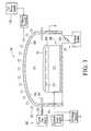
- FIG. 3is a schematic sectional side view of an etching chamber
- FIG. 4is a schematic sectional side view of a cleaning chamber
- FIGS. 5 a and 5 bare flow charts illustrating substrate cleaning processes
- FIGS. 6 a and 6 bare flow charts illustrating other versions of substrate cleaning processes.
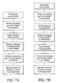
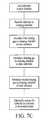
- FIGS. 7 a - 7 care flow charts illustrating other versions of substrate cleaning processes.
- the process and apparatus of the present inventionare useful for processing substrates, such as semiconductor wafers, but may also be used for other processes or for processing other substrates, such as printed circuit boards, flat panel displays, and liquid crystal displays.
- substratessuch as semiconductor wafers
- substratessuch as printed circuit boards, flat panel displays, and liquid crystal displays.
- the descriptionrepresents illustrative embodiments of the invention and is not intended to limit the invention.
- a substrate 30such as a substratum 35 having one or more materials, such as layers 40 , 45 , 50 , thereon as shown in FIG. 1 a , may be processed.
- These layersare often superimposed on one another and may comprise dielectric layers comprising, for example, silicon dioxide, undoped silicate glass, phosphosilicate glass (PSG), borophosphosilicate glass (BPSG), Si 3 N 4 , or TEOS deposited glass; semiconducting layers comprising, for example, silicon-containing layers such as polysilicon or a silicon compound; and electrically conducting layers such as metal-containing layers comprising, for example, aluminum, copper, titanium, titanium nitride, or metal silicide such as tungsten silicide and cobalt silicide.
- dielectric layerscomprising, for example, silicon dioxide, undoped silicate glass, phosphosilicate glass (PSG), borophosphosilicate glass (BPSG), Si 3 N 4 , or TEOS deposited glass
- semiconducting layers
- Suitable etchant gases for etching layers on the substrate 30include for example, HCl, BCl 3 , HBr, Br 2 , Cl 2 , CCl 4 , SiCl 4 , SF 6 , F 2 , NF 3 , HF, CF 3 , CF 4 , CH 3 F, CHF 3 , C 2 H 2 F 2 , C 2 H 2 F 4 , C 2 H 4 F 2 , C 2 F 6 , C 3 F 8 , C 4 F 8 , C 2 HF 5 , C 4 F 10 , CF 2 Cl 2 , CFCl 3 , O 2 , N 2 , He, and mixtures thereof.
- the etchant gasis selected to provide high etch rates, and highly selective etching of the particular layers or materials that are being etched.
- multiple etchant gas compositions having first, second, third, etc. compositionsmay be sequentially introduced into the chamber to etch each particular layer.
- FIG. 1 ashows a version of a substrate 30 having material formed on a substratum 35 .
- the substratum 35may comprise semiconducting material, such as silicon, gallium arsenide, and the like.
- the material on the substratum 35may comprise (i) a diffusion barrier material 40 comprising, for example, silicon oxynitride, organic anti-reflective layer (ARC), titanium, tungsten, titanium-tungsten, or titanium nitride, (ii) an electrically conductive material 45 comprising, for example, titanium, tungsten, aluminum, copper or similar metal or alloys thereof, and optionally silicon, and (iii) an anti-reflective material 50 comprising, for example, silicon, titanium nitride, or titanium tungsten.
- a diffusion barrier material 40comprising, for example, silicon oxynitride, organic anti-reflective layer (ARC), titanium, tungsten, titanium-tungsten, or titanium nitride
- An oxide layer(not shown), such as SiO 2 , may also be provided below the diffusion barrier layer 40 .
- a patterned etch-resistant material 60 of, for example, photoresist, such as polymeric photoresist, or electron-beam resistoverlies the layers.
- Etchant gasmay be provided to etch the exposed portions of the layers to form apertures 65 , such as lines, trenches, holes or vias, that extend through one or more of the layers and which form features 67 on the substrate 30 , as schematically illustrated in FIG. 1 b.
- remnant resist 60 and etchant residue 70 remaining on the substrate 30may be removed in one or more cleaning processes to provide a clean substrate surface for subsequent processing that is substantially resistant to corrosion.
- the remnant resist 60is the portion of the resist material that remains on the substrate 30 after the etching process and may comprise any material that is relatively resistant to etchant gas used to etch one or more underlying materials on the substrate 30 .
- the remnant resist 60comprises residual polymeric photoresist or oxide hard mask. Suitable polymeric photoresist materials are commercially available from Shipley Co., Marlboro, Mass., or Tokyo Ohka Kogyo (TOK) Co., Ltd., Kawasaki, Japan.
- the etchant residue 70 on the featuresmay comprise (i) residual species 75 , for example residual halogen radicals, such as chlorine or fluorine, metal containing species, such as one or more metal oxides, or byproduct compounds
- the sidewall depositsmay comprise (i) organic compounds containing carbon and hydrogen, (ii) metal from the metal-containing layers, such as aluminum or titanium, and (iii) etchant gas species such as chlorine, boron and/or nitrogen.
- the composition and stoichiometry of the sidewall deposits 80depend upon the chemical composition of the material being etched, the resist material 60 , and the etchant gases used to etch the features 67 .
- the etchant residue 70comprises both residual species 75 and sidewall deposits 80 .
- the residual speciesmay comprise one or more of Al 2 O 3 , TiO 2 , CuO, and SiO 2 .
- the sidewall depositsmay comprise one or more of carbon, hydrogen, nitrogen, one or more halogens, oxygen, silicon, and metals.
- cleaningit is meant that one or more of the remnant resist, residual species, and sidewall deposits is at least partially removed from a substrate 30 or inactivated.
- the substrate 30may be etched and cleaned in a multi-chamber apparatus 100 comprising one or more etching chambers 110 for etching the substrate 30 , and one or more cleaning chambers 120 for removing remnant resist 60 and/or removing or inactivating etchant residue 70 that remain on the substrate 30 after the etching process.
- the etching chamber 110 , cleaning chamber 120 , a transfer chamber 125 , and a load lock chamber 130may be interconnected in a vacuum sealed environment that may be maintained at a low pressure to reduce contamination of the substrate 30 .
- a robotic arm 135transfers a substrate 30 from the load lock chamber 130 to the transfer chamber 125 and then to one of the processing chambers.
- the substrate 30may be etched in a process chamber 110 , such as for example, a DPS type Metal Etch Centura chamber, schematically illustrated in FIG. 3, and from Applied Materials, Inc. in Santa Clara, Calif.
- the particular embodiment of the process chamber 110 shown hereinis provided only to illustrate the invention, and should not be used to limit the scope of the invention.
- the chamber 110comprises a support 140 within a process zone 145 in the chamber 110 .
- a substrate 30may be positioned on the support 140 by the robotic arm 135 .
- the substrate 30may be held in place during the etching process using a mechanical or electrostatic chuck 150 with grooves 155 in which a coolant gas, such as helium, is held to control the temperature of the substrate 30 .
- the chamber 110may be maintained at a low pressure and process gas may be introduced into the chamber 110 through a gas supply 160 having a gas source 162 and gas inlets 164 peripherally disposed about the substrate 30 .
- a showerhead gas distributer(not shown) may be positioned above the substrate 30 .
- the process gasmay be energized by a gas energizer that couples an energetic electromagnetic field into the process zone 145 , such as an inductive, capacitive, or microwave field.
- an energetic electromagnetic fieldsuch as an inductive, capacitive, or microwave field.
- an inductor coil 165 adjacent to the process chamber 110forms an inductive electric field in the chamber 110 when powered by a coil power supply 170 operated using, for example, an RF voltage at a source power level that may be from about 200 Watts to about 2000 Watts.
- a capacitive electric fieldmay be formed in the chamber 110 .
- At least a portion of the support 140may be electrically conductive to serve as a cathode electrode 175 .
- the cathode electrode 175in conjunction with sidewalls of the chamber 110 which may be electrically grounded to serve as an anode electrode 180 , form process electrodes in the process zone 145 that may capacitively couple to energize the process gas.
- the cathode 175may be powered by an electrode power supply 185 operated using, for example, an RF voltage at a power level of from about 10 Watts to about 1000 Watts.
- the capacitive electric fieldis substantially perpendicular to the plane of the substrate 30 , and may accelerate the plasma species toward the substrate 30 to provide more vertically oriented anisotropic etching of the substrate.
- the frequency of the RF voltage applied to the process electrodes 175 , 180 , and/or the inductor coil 165is typically from about 50 KHz to about 60 MHz, and more typically about 13.56 MHz.
- the cathode 175is also an electrode in a dielectric in the electrostatic chuck 150 .
- the ceiling 190 of the process chamber 110can be flat or rectangular shaped, arcuate, conical, dome-shaped, or multi-radius dome-shaped.
- the inductor coil 165covers at least a portion of the ceiling 190 of the process chamber 110 in the form of a multi-radius dome-shaped inductor coil having a “flattened” dome shape that provides more efficient use of plasma source power and increased plasma ion flux uniformity directly over the substrate 30 center.
- the plasma formed in the process zone 145may also be enhanced using magnetically enhanced reactors (not shown), in which a magnetic field generator, such as a permanent magnet or electromagnetic coils, are used to apply a magnetic field in the process zone 145 to increase the density and uniformity of the plasma.
- the magnetic fieldmay comprise a rotating magnetic field with the axis of the field rotating parallel to the plane of the substrate 30 , as described in U.S. Pat. No. 4,842,683, which is incorporated herein by reference in its entirety.
- Spent process gas and etchant residueare exhausted from the process chamber 110 through an exhaust system 195 capable of achieving a low pressure in the process chamber 110 .
- a throttle valve 200is provided in the exhaust for controlling the pressure in the chamber 110 .
- an optical endpoint measurement system(not shown) may be used to determine completion of the etching process for a specific layer by measuring, for example, the change in light emission of a particular wavelength corresponding to a detectable gaseous species or by other interferometric techniques.
- an energized process gascomprising etchant gas may be provided in the process zone 145 .
- energized process gasit is meant that the process gas is activated or energized to form one or more dissociated species, non-dissociated species, ionic species, and neutral species.
- the etchant gas compositionmay be selected to provide high etch rates, and highly selective etching of a particular layer or layers that are being etched.
- the etchant gasesmay comprise one or more of halogen-containing gases, such as one or more of Cl 2 , BCl 3 , CCl 4 , SiCl 4 , CF 4 , NF 3 , SF 6 , Br 2 , HBr, BBr 3 , CHF 3 , C2F2, and the like, and optionally, one or more additive gases, such as inert or non-reactive gases, such as H 2 , N 2 , O 2 , He—O 2 , and the like.
- halogen-containing gasessuch as one or more of Cl 2 , BCl 3 , CCl 4 , SiCl 4 , CF 4 , NF 3 , SF 6 , Br 2 , HBr, BBr 3 , CHF 3 , C2F2, and the like
- additive gasessuch as inert or non-reactive gases, such as H 2 , N 2 , O 2 , He—O 2 , and the like.
- the anti-reflective material 50is etched by exposing the substrate 30 to an energized process gas comprising etchant gas comprising, for example, about 90 sccm Cl 2 and about 30 sccm BCl 3 at a pressure of about 8 mTorr, a source power level of about 1600 Watts, a bias power level of about 145 Watts, a backside helium pressure of about 4 Torr and a cathode temperature of about 50° C.
- etchant gascomprising, for example, about 90 sccm Cl 2 and about 30 sccm BCl 3 at a pressure of about 8 mTorr, a source power level of about 1600 Watts, a bias power level of about 145 Watts, a backside helium pressure of about 4 Torr and a cathode temperature of about 50° C.
- the electrically conductive material 45may then be etched by an energized process gas comprising etchant gas comprising, for example, about 80 sccm Cl 2 , about 5 sccm BCl 3 , and about 10 sccm CHF 3 at a pressure of about 14 mTorr, a source power level of about 1600 Watts, a bias power level of about 150 Watts, a backside helium pressure of about 8 Torr and a cathode temperature of about 50° C.
- etchant gascomprising, for example, about 80 sccm Cl 2 , about 5 sccm BCl 3 , and about 10 sccm CHF 3 at a pressure of about 14 mTorr, a source power level of about 1600 Watts, a bias power level of about 150 Watts, a backside helium pressure of about 8 Torr and a cathode temperature of about 50° C.
- the diffusion barrier layer 40may be etched by introducing an energized process gas comprising etchant gas comprising, for example, about 30 sccm Cl 2 , about 5 sccm BCl 2 , and about 30 sccm N 2 or Ar at a pressure of about 10 mTorr, a source power level of about 1600 Watts, a bias power level of about 125 Watts, a backside helium pressure of about 8 Torr and a cathode temperature of about 50° C.
- etchant gascomprising, for example, about 30 sccm Cl 2 , about 5 sccm BCl 2 , and about 30 sccm N 2 or Ar at a pressure of about 10 mTorr, a source power level of about 1600 Watts, a bias power level of about 125 Watts, a backside helium pressure of about 8 Torr and a cathode temperature of about 50° C.
- the substrate 30may be dechucked and lifted from the support 140 by, for example, a pneumatic lifting apparatus which raises lift pins (not shown) in the support 140 to raise the substrate 30 from the surface of the support 140 .
- the robotic transport arm 135may be inserted between the substrate 30 and the support 140 to lift the substrate 30 off the lift pins. Thereafter, the lift pins are retracted into the support 140 , and the robotic arm 135 transports the substrate 30 out of the etching chamber 110 and into the transfer chamber 125 .
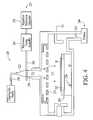
- the substrate 30may be transferred from the transfer chamber 125 to a cleaning chamber 120 , such as for example, an Advanced Strip and Passivation, (ASP) chamber, schematically illustrated in FIG. 4, and commercially available from Applied Materials Inc. in Santa Clara, Calif.
- a cleaning chamber 120such as for example, an Advanced Strip and Passivation, (ASP) chamber, schematically illustrated in FIG. 4, and commercially available from Applied Materials Inc. in Santa Clara, Calif.
- the cleaning chamber 120 shown hereinis provided only to illustrate the process of the present invention, and should not be used to limit the scope of the invention, because other cleaning chambers can also be used to clean the substrate 30 , including the process chamber 110 shown in FIG. 3 .
- the substrate 30is placed on a support 210 by the robotic arm 135 , and optionally held in place during processing by a mechanical or electrostatic chuck 212 .
- an energized process gas comprising cleaning gasis provided to clean the substrate 30 held on the support 210 in a process zone 215 .
- the support 210supports the substrate 30 in the process zone 215 and may optionally comprise an electrostatic chuck 212 .
- a heat sourcesuch as infrared lamps 220 , can be used to heat the substrate 30 .
- the process gas comprising cleaning gasmay be introduced through a gas distributor 222 into a remote plasma generation zone 225 in a remote chamber 230 .
- remoteit is meant that the center of the remote chamber 230 is at a fixed upstream distance from the center of a process zone 215 in the cleaning chamber 120 .
- the cleaning gasis activated by coupling microwave or RF energy into the remote chamber 230 , to energize the cleaning gas and cause ionization or dissociation of the cleaning gas components, prior to its introduction through a diffuser 235 , such as a showerhead diffuser, into the process zone 215 .
- the process gasmay be energized in the process zone 215 .
- Spent cleaning gas and residuemay be exhausted from the cleaning chamber 120 through an exhaust system 240 capable of achieving a low pressure in the cleaning chamber.
- a throttle valve 245 in the exhaust 240is used for maintaining a chamber pressure from about 150 mTorr to about 3000 mTorr.
- the remote chamber 230comprises a tube shaped cavity containing at least a portion of the remote plasma zone 225 .
- Flow of cleaning gas into the remote chamber 230is adjusted by a mass flow controller or gas valve 250 .
- the remote chamber 230may comprise walls made of a dielectric material such as quartz, aluminum oxide, or monocrystalline sapphire that is substantially transparent to microwaves and is non-reactive to the cleaning gas.
- a microwave generator 255is used to couple microwave radiation to the remote plasma zone 225 of the remote chamber 230 .
- a suitable microwave generator 255is an “ASTEX” Microwave Plasma Generator commercially available from the Applied Science & Technology, Inc., Woburn, Mass.
- the microwave generator assembly 255may comprise a microwave applicator 260 , a microwave tuning assembly 265 , and a magnetron microwave generator 270 .
- the microwave generatormay be operated at a power level of about 200 to about 3000 Watts, and at a frequency of about 800 MHz to about 3000 MHz.
- the remote plasma zone 225is sufficiently distant from the process zone 215 to allow recombination of some of the dissociated or ionized gaseous chemical species.
- the resultant reduced concentration of free electrons and charged species in the activated cleaning gasminimizes charge-up damage to the active devices on the substrate 30 , and provides better control of the chemical reactivity of the activated gas formed in the remote plasma zone 225 .
- the center of the remote plasma zone 225is maintained at a distance of at least about 50 cm from the center of the process zone 215 .
- a cleaning processmay be performed in the cleaning chamber 120 by exposing the substrate 30 to energized process gas comprising cleaning gas to, for example, remove remnant resist 60 and/or to remove or inactivate etchant residue 70 remaining on the substrate after the substrate is etched.
- Remnant resist 60may be removed from the substrate 30 in a stripping (or ashing) process by exposing the substrate 30 to energized process gas comprising stripping gas.
- Stripping gasmay comprise, for example, one or more of O 2 , N 2 , H 2 , H 2 O, NH 3 , CF 4 , C 2 F 6 , CHF 3 , C 3 H 2 F 6 , C 2 H 4 F 2 , or CH 3 F.
- a suitable stripping gas for stripping polymeric resist materialcomprises (i) oxygen, and optionally (ii) an oxygen activating gas or vapor, such as water vapor, nitrogen gas, or fluorocarbon gas, the fluorocarbon gases including any of those listed above.
- the oxygen activating gasincreases the concentration of oxygen radicals in the stripping gas.
- the stripping gas compositionmay comprise oxygen and nitrogen in a volumetric flow ratio of about 6:1 to about 200:1, and more preferably from about 10:1 to about 12:1.
- a suitable gas flow ratecomprises 3000 to 3500 sccm of O 2 and 300 sccm of N 2 .
- a stripping gascomprises about 3500 sccm O 2 about 200 sccm N 2 and optionally about 300 sccm H 2 O, that is energized at a power level of about 1400 Watts and introduced into the cleaning chamber 120 at a pressure of about 2 Torr for about 15 seconds.
- the water vapor content in the stripping gasshould be less than about 20% by volume of the combined oxygen and nitrogen gas content to provide adequate stripping rates.
- a suitable ratio of the volumetric water vapor flow V H2O to the combined volumetric flow of oxygen and nitrogen (V O2 +V N2 )is from about 1:4 to about 1:40, and more preferably about 1:10.
- suitable stripping gasesare gases capable of stripping oxide, such as halogen containing gases, including CF 4 , C 2 F 6 , CHF 3 , C 3 H 2 F 6 , C 2 H 4 F 2 and HF.
- the substratemay be exposed to the stripping gas for a period of time of from about 10 seconds to about 1000 seconds, and more preferably for about 45 seconds.
- a single stripping stepmay be performed or multiple stripping steps may be performed, as discussed in U.S. Pat. No. 5,545,289, which is incorporated herein by reference in its entirety.
- the cleaning processmay also comprise post-etch passivation of the substrate 30 , particularly when conductive material 45 has been etched in the etching process, to remove or inactivate corrosive residue species 75 on the substrate 30 .
- energized process gascomprising passivating gas may be provided in the process zone 215 .
- the passivating gas compositionis selected to remove or inactivate corrosive etchant residue, such as residual species 75 or to prevent the formation of corrosive or contaminant materials on the etched substrate 30 .
- Passivating gasmay comprise one or more of H 2 O, NH 3 , H 2 O 2 , O 2 , N 2 , CF 4 , C 2 F 6 , CHF 3 , H 2 , C 3 H 2 F 6 , C 2 H 4 F 2 , or CH 3 F.
- any gas or vapor containing hydrogencan serve as the passivating gas, including hydrogen, water vapor, ammonia, methanol, hydrogen sulfide, and mixtures thereof.
- the passivating gasesinclude (i) ammonia and oxygen, or (ii) water vapor, with optional oxygen and nitrogen.
- the volumetric flow ratio of ammonia to oxygenis preferably from about 1:1 to about 1:50, more preferably from about 1:5 to about 1:20, and most preferably about 1:10.
- a preferred gas flowcomprises 300 sccm NH 3 and 3000 sccm O 2 .
- a passivating gascomprising at least about 80 volume % H 2 O, and preferably about 100 volume % H 2 O, can be used to passivate the etchant residue 75 .
- a passivating gascomprises about 500 sccm H 2 O energized at a power level of about 1400 Watts and introduced into the cleaning chamber 120 at a pressure of about 2 Torr for about 15 seconds.
- an inert carrier gassuch as argon or helium can be passed through the bubbler to transport water vapor to the vacuum chamber.
- oxygen, nitrogen or other additivecan be added to the passivating gas to enhance passivating.
- the passivating gascomprises at least about 20 volume % H 2 O. The effect of the oxygen and nitrogen addition depends on the ratio of the volumetric flow rate of water vapor (V H2O ) to the combined volumetric flow rates of oxygen and nitrogen (V O2 +V N2 ).
- a suitable volumetric ratio of water vapor flow rate V H2O to combined volumetric flow rates of oxygen and nitrogen (V O2 +V N2 ) for use as a passivating gasis at least about 1:2, more preferably from about 1:2 to about 2:1, and most preferably about 1:1.
- the passivationmay be either a single step or multiple steps.
- the substrateis exposed to the passivating gas for a period of time of from about 10 seconds to about 100 seconds, and more preferably for about 45 seconds.
- a multi-cycle passivation processfor example a three cycle process, has been discovered to be particularly effective in preventing corrosion.
- the substratemay be heated during the stripping and/or the passivation processes.
- the lamps 220may be used to heat the substrate to a temperature of at least about 150° C., and even at least about 200° C., and preferably to a temperature of at least about 250° C. Heating the substrate 30 improves the remnant resist removal rate and may also improve the removal rate of some etchant residue, such as Cl in the sidewall deposits 80 , because the Cl can more readily diffuse out of the sidewall deposits.
- the elevated temperaturesalso enhance the surface oxidation, when O 2 -containing strip density is used, of the etched metal, making them less susceptible to corrosion.
- the substrate 30may be transferred to a wet-cleaning chamber (not shown) where the substrate 30 may be exposed for a short period to a solvent to complete the removal of remnant resist 60 and etchant residue 70 .
- a wet-cleaning chamberBy first cleaning the substrate 30 in the cleaning chamber, the solvent exposure time and/or the solvent strength may be minimized thereby reducing the deleterious effects of the solvent, such as attack of the etched features 67 which may result in sidewall etching and/or critical dimension loss.
- a wet solventsuch as for example EKC Z65 or similar solvents from EKC Technology, Inc.
- the removal of remnant resist 60 or etchant residue 70can be improved by exposing the substrate to a process gas comprising a treating gas before, during, or after the cleaning process.
- the treating gasmay be selected to enhance or improve the cleaning of the substrate thereby further reducing the need to expose the substrate 30 to a wet solvent after a cleaning process.
- the treating processmay be performed in the etching chamber 110 , in the cleaning chamber 120 , or in a separate chamber.
- the treating gascomprises a halogen.
- the treating gascomprises a hydrogen species and a halogen species.
- the treating gasmay comprise one or more of HCl, HBr, and HF.
- the treating gasmay comprise H 2 and one or more of Cl 2 , Br 2 , and F 2 , or any composition that provides a hydrogen species, such as one or more of NH 3 , CHF 3 , CH 2 F 2 , CH 3 F or H 2 , H 2 O and equivalents, and a halogen species, such as one or more of HCl, HBr, HF, Cl 2 , Br 2 , F 2 , CF 4 , NF 3 , SF 6 , CHF 3 , C 2 F 6 , CH 2 F 3 , CH 3 F and, and equivalents.
- a hydrogen speciessuch as one or more of NH 3 , CHF 3 , CH 2 F 2 , CH 3 F or H 2 , H 2 O and equivalents
- a halogen speciessuch as one or more of HCl, HBr, HF, Cl 2 , Br 2 , F 2 , CF 4 , NF 3 , SF 6 , CHF 3 , C 2 F 6
- the substrate 30may be pre-treated prior to cleaning by exposing the etched substrate 30 to an energized process gas comprising treating gas.
- the treating gasmay be provided in the etching chamber 110 before the substrate 30 is transferred to the cleaning chamber 120 .
- the substrate 30may be treated in the cleaning chamber 120 .
- the etching, treating, and cleaning processesare all performed in the same chamber. In the FIG.
- an energized process gas comprising treating gasis provided in the process zone 145 of the etching chamber 110 .
- an energized process gas comprising treating gasis provided in the process zone 215 of the cleaning chamber 120 .
- cleaning gasis provided in the process zone 215 to remove the remnant resist 60 and/or to remove the etchant residue 70 from the substrate 30 .
- an effective treating gascomprises chlorine species, and in one version comprises a hydrogen species and a chlorine species.
- the substrate 30may be exposed to an energized process gas comprising one or more of (i) HCl, (ii) H 2 and Cl 2 , and (iii) a hydrogen species containing gas and a chlorine species containing gas.
- Treating gas comprising a hydrogen species and a chlorine speciesis effective in at least partially removing sidewall deposits 80 , such as polymeric sidewall deposits, on the substrate 30 .
- the hydrogen species and chlorine species containing treating gasis also particularly effective in removing or in aiding in the removal of sidewall deposits 80 on etched features 67 having tapered profiles. It is believed that treating gas comprising HCl or H 2 /Cl 2 reacts with sidewall deposits 80 to remove them from the etched features 67 .
- the chlorine speciesmay react with metal species, such as aluminum, and hydrogen species may react with organic components, such as carbon. In one version, it has been shown to be advantageous to combine a pretreatment process and a passivation process in order to significantly improve corrosion prevention.
- FIGS. 6 a and 6 bAnother version of the invention is shown in FIGS. 6 a and 6 b .
- the substrate 30is exposed to an energized process gas comprising treating gas after a cleaning process.
- the treating processmay be performed in the cleaning chamber 120 after the cleaning process.
- the treating gasmay be provided in the process zone 215 of the cleaning chamber 120 before or after completion of the cleaning process.
- the substrate 30may be transferred to a treating chamber, such as a second cleaning chamber 120 , where it can be treated.
- a treating chambersuch as a second cleaning chamber 120
- the treating gasmay be selected to remove remnant resist 60 or etchant residue 70 that remains on the substrate 30 after the cleaning process or may soften and/or loosen the remaining resist 60 or etchant residue 70 so that it may be removed in a deionized water bath or with a shortened exposure to a wet solvent.
- a treating gas comprising fluorineis effective in treating the substrate 30 by, for example, softening or loosening remaining etchant residue 70 on the substrate 30 after a cleaning process.
- a treating gas comprising a hydrogen speciessuch as one or more of NH 3 , H 2 O, H 2 and a fluorine species, such as NF 3 , CF 4 , F 2 , SF 6 , C 2 F 6 , and CHF 3
- a hydrogen speciessuch as one or more of NH 3 , H 2 O, H 2
- a fluorine speciessuch as NF 3 , CF 4 , F 2 , SF 6 , C 2 F 6 , and CHF 3
- a treating gascomprising NH 3 and a fluorine-containing gas, such as one or more of NF 3 , CF 4 , has been shown to allow for effective etchant residue 70 removal without the need for exposing the substrate 30 to a wet solvent. It is believed that by energizing the NH 3 and the fluorine-containing gas, hydrogen and fluorine species are generated that react with and solubilize the sidewall deposits 80 , to render the deposits removable by a de-ionized water rinse, for example.
- a fluorine-containing gassuch as one or more of NF 3 , CF 4
- a particular mixture of NH 3 and NF 3can produce a film on the substrate 30 that may release HF when exposed to an aqueous solution or other polar solvent. Accordingly, HF can be liberated and residue removed simultaneously during the wet process steps (e.g. Dl rinse).
- the treating gasmay also be introduced under process conditions selected to remove process residue from the chamber surfaces, such as surfaces of walls or components in the chamber 120 .
- residuemay be generated during the cleaning process, and the residue may get deposited on the surfaces.
- a halogen-containing treating gasis introduced in the process zone 215 of the cleaning chamber 120 after or during a cleaning process to simultaneously treat the substrate 30 and to remove residue from the chamber surfaces.
- the treating gasmay be introduced in a volumetric flow rate of about 80 sccm to about 1000 sccm, more preferably about 300 sccm to about 500 sccm, and most preferably about 320 sccm, under the following process conditions: 80 sccm NF 3 , 240 sccm NH 2 , 2 torr, 1.4 kw for 200 mm substrate processing chamber.
- the treating gasmay comprise one or more of H 2 , F 2 , NH 3 , NF 3 , CF 4 , CH 4 , CH 3 F, and CHF 3 .
- the treating gasmay also be used to clean residue from the chamber surfaces in a version of the invention where the substrate 30 is etched, cleaned, and treated in the same chamber, thereby removing etchant residue and/or cleaning residue from the chamber surfaces.
- treatment in the etch chamber using HCl or H 2 /Cl 2can remove etchant residues from the wafer and etch by-product deposition from chamber surfaces.
- the effectiveness of the treating gas in the processes of FIGS. 5 a and 5 b or FIG. 6 a or 6 bmay be increased by selecting process conditions that maximally treat the substrate 30 without damaging the etched features 67 thereon.
- the treating gasmay comprise HCl in a volumetric flow rate of from about 80 sccm to about 250 sccm, more preferably from about 100 sccm to about 200 sccm, and most preferably about 150 sccm in the etching chamber 110 or in equivalent volumetric flow rates in the cleaning chamber 120 , for 200 mm substrate processing chamber.
- the substrate 30may be exposed to the treating gas for a period of at least about 30 seconds, more preferably at least about 120 seconds, and most preferably about 240 seconds with the chamber 110 maintained at a pressure of about 25 mTorr, a source power of about 500 watts, and a temperature of about 150° C.
- the treating gasfor a period of at least about 30 seconds, more preferably at least about 120 seconds, and most preferably about 240 seconds with the chamber 110 maintained at a pressure of about 25 mTorr, a source power of about 500 watts, and a temperature of about 150° C.
- the treating gasmay comprise NH 3 in a volumetric flow rate of from about 80 sccm to about 1000 sccm, more preferably from about 100 sccm to about 400 sccm, and most preferably about 240 sccm and NF 3 in a volumetric flow rate of from about 5 sccm to about 200 sccm, more preferably from about 20 sccm to about 120 sccm, and most preferably about 80 sccm in the cleaning chamber 120 .
- the volumetric flow ratio of NH 3 to NF 3may be from about 1:1 to about 10:1, more preferably from about 2:1 to about 4:1, most preferably 3:1.
- the effectiveness of the treating gasmay also be increased by applying a bias to the substrate 30 .
- a bias powerof from about 0 watts to about 150 watts, more preferably from about 20 watts to about 100 watts, and most preferably about 50 watts may be applied to the process electrode 175 in the etching chamber 110 .
- the application of bias powerhas been shown by scanning electron microscope (SEM) data to significantly improve the resist material 60 and the etchant residue 70 removal during the treating process, leaving less resist 60 and residue 70 to be removed during the cleaning process.
- Bias powermay also increase the effectiveness of the treating process of FIGS. 6 a and 6 b and may be, for example, from about 0 to 600 watts, more preferably from about 50 watts to about 300 watts, and most preferably about 150 watts.
- the temperature of the substrate 30may also be selected to increase the effectiveness of the cleaning and the treating processes.
- a substrate temperature of from about 20° C. to about 100° C.is effective in treating the substrate 30 , for example by solubilizing the sidewall deposits 80 . This is believed to be due to enhancing adsorption of the reactive species onto the substrate and minimizing chemical attack of the substrate.
- the substrate 30is maintained at a temperature of from about 20° C. to about 100° C.
- the substrateis cleaned in a stripping and passivating process at a temperature of about 250° C. and then cooled to a temperature of about 50° C.
- the substrate 30When the substrate 30 is cleaned and treated in the same chamber, for example as shown in FIG. 6 a , the substrate may be rapidly cooled, such as by circulating a heat transfer fluid through the support 210 in the chamber.
- one chambermay be maintained at a first temperature, such as about 250° C.
- the second chambermay be maintained at a second temperature, such as from about 30° C. to about 100° C.
- the integrated process sequence of the versions described aboveprovides effective and improved remnant resist 60 and etchant residue 70 removal.
- the cleaned substrateoften does not require wet solvent exposure.
- the versions of FIGS. 5 a , 5 b , 6 a , and 6 bprovide a large process window for etch processes by providing improved strip/residue removal.
- the inventionallows for the removal of resist 60 and residue 70 at relatively low temperatures with a de-ionized water rinse following exposure of the substrate 30 to to relatively high temperature oxygen-containing and/or water vapor containing gases. This is advantageous because the high temperature provides high strip rates and improved corrosion control.
- the inventionprovides the ability to incorporate additional processes, such as high temperature nitrogen exposure, which can improve corrosion resistance, but which necessitates wet solvent exposure of the substrate 30 in conventional processes.
- the substrate 30may be exposed to an energized process gas comprising a first treating gas before a cleaning process and exposed to an energized process gas comprising a second treating gas after the cleaning process.
- This versionprovides increased removal of resist 60 and etchant residue 70 and even further reduces the need to expose the substrate 60 to a wet solvent.
- the first and second treating gasesmay be the same gas or different gas.
- one of the treating gasesmay comprise chlorine.
- one of the treating gasesmay comprise fluorine.
- the first treating gascomprises a hydrogen species and a chlorine species, such as HCl
- the second treating gascomprises a hydrogen species and a fluorine species, such as one or more of NH 3 and H 2 and one or more of NF 3 , CF 4 , and SF 6 .
- the first treating gasmay be introduced in the etching chamber 110 after or during an etching process
- the second treating gasmay be introduced in the cleaning chamber after or during a cleaning process.
- the cleaning process and the second treating processare performed in separate chambers.
- the first and second treating gasesare provided in the cleaning chamber.
- the etching, cleaning and first and second treating processesmay be performed in the same chamber.
Landscapes
- Engineering & Computer Science (AREA)
- Physics & Mathematics (AREA)
- General Physics & Mathematics (AREA)
- Microelectronics & Electronic Packaging (AREA)
- Manufacturing & Machinery (AREA)
- Computer Hardware Design (AREA)
- Condensed Matter Physics & Semiconductors (AREA)
- Power Engineering (AREA)
- Plasma & Fusion (AREA)
- Chemical & Material Sciences (AREA)
- Chemical Kinetics & Catalysis (AREA)
- General Chemical & Material Sciences (AREA)
- Drying Of Semiconductors (AREA)
- Cleaning Or Drying Semiconductors (AREA)
Abstract
Description
The present invention relates to cleaning a substrate.
In the manufacture of integrated circuits, active and passive devices are formed on a substrate, such as a semiconductor wafer, by alternately depositing and etching layers of dielectric, semiconducting, and conducting materials, such as silicon dioxide, polysilicon, and metal compounds and alloys. These layers may be etched to form a pattern of etched features by providing a resist layer of photoresist and/or oxide hard mask on the substrate, and using lithography or energized gas to expose and pattern the resist layer. The portions of the layers adjacent to the patterned resist features are etched to form a predefined pattern of gates, vias, contact holes, trenches, and/or metal interconnect lines. Etching is typically performed using a capacitively or inductively coupled plasma of halogen-containing gases, as for example described inSilicon Processing for the VLSI Era, Vol.1, Chapter 16, by Wolf and Tauber, Lattice Press, 1986, which is incorporated herein by reference.
The etching process may leave remnant resist and etchant residue on the substrate. Remnant resist are those residual resist portions that are not etched by the etchant gases, and which remain on the substrate after the etching process. The etchant residue may comprise residual species and/or sidewall deposits on the sidewalls of the etched features. The residual species may result from adsorption of halogen-containing etchants on the etched features which may lead to corrosion of the metal-containing features. The sidewall deposits may be formed during the etching process by reaction of the etchant gases, the metal-containing layers, and the resist, and by condensation of the reaction residue on the sidewalls of the features. One method of cleaning an etched substrate is a dry cleaning method in which a plasma of a gas is used to remove remnant resist remaining on the substrate in a stripping (or ashing) process and to remove or inactivate residual halogen-containing species in a passivating process. The sidewall deposits on the substrate are typically removed by wet chemical etching methods or they can be at least partially removed in a dry cleaning process.
Conventional stripping methods which use a plasma of oxygen, nitrogen or water vapor, can be used to strip remnant resist from the substrate. These conventional stripping techniques are sometimes ineffective at stripping all the resist from the substrate, particularly when the polymeric resist is hardened by exposure to a plasma. For oxide hard mask resists, the oxide layer can be stripped or can be left on the substrate. Typically, remnant oxide hard mask is left on the substrate and a dielectric layer is deposited on the remnant oxide in a subsequent process step. In addition, adequate stripping processes generally compromise process throughput. The stripping process may also harden sidewall deposits making the deposits difficult to remove.
In passivating techniques, the etchant residue on the substrate is removed or inactivated to, for example, reduce post-etch corrosion problems by using a passivating gas, such as ammonia and/or water vapor. One limitation of conventional passivating techniques is that they often only prevent post-etch corrosion of the substrate for short periods, typically ranging from about 1 to 5 hours after exposure of the substrate to ambient moisture. The short corrosion resistant period is undesirable because post-etch processing steps may need to be performed within 1 to 2 hours after the substrate is first exposed to the atmosphere, resulting in a tight or inflexible production schedule. Often, the substrate cannot be etched, or if already etched, cannot be removed from the chamber in order to avoid corrosion.
Due to the shortcomings of the conventional dry cleaning processes, remnant resist and/or etchant residues are often removed in a wet-cleaning process in which the substrate is exposed to wet solvents. However, the wet-cleaning process also suffers from several disadvantages. For example, residue removal is often not complete, resulting in inconsistently processed substrates. In addition, the solvents may attack the metal-containing features on the substrate, particularly when very small features are etched on the substrate. The solvents used may also be costly and may generate hazardous chemical waste that is difficult to dispose of.
Thus, there is a need for a process and apparatus for cleaning a substrate to, for example, remove remnant resist and etchant residue on the substrate. It is further desirable to reduce post-etch corrosion. It is still further desirable to be able to clean a substrate while reducing the need to expose the substrate to a wet solvent.
The present invention satisfies these needs. In one aspect of the present invention, a substrate processing method comprises exposing a substrate to an energized process gas to etch the substrate, exposing the substrate to an energized cleaning gas, and before, during, or after exposing the substrate to an energized cleaning gas, exposing the substrate to an energized treating gas comprising a halogen species and a hydrogen species.
In another aspect of the invention, a substrate processing method comprises exposing a substrate to an energized process gas to etch the substrate and exposing the substrate to an energized treating gas comprising a chlorine species.
In another aspect of the invention, a substrate processing method comprises exposing a substrate to an energized process gas to etch the substrate and exposing the substrate to an energized treating gas comprising a fluorine species and a hydrogen species.
In another aspect of the invention, a method of treating an etched substrate comprises exposing the etched substrate to an energized process gas comprising a first halogen species and exposing the etched substrate to an energized process gas comprising a second halogen species.
In another aspect of the invention, a method of cleaning an etched substrate comprises exposing a substrate to a cleaning gas; and after this, exposing the substrate to an energized treating gas comprising one or more of NH3and H2.
In another aspect of the invention, a substrate processing method comprises exposing a substrate to an energized process gas to etch the substrate in a process zone and exposing the substrate to an energized treating in the process zone.
In another aspect of the invention, a method of treating an etched substrate comprises exposing the etched substrate to an energized process gas comprising oxygen species while maintaining the substrate at a temperature of at least about 200° C., treating the substrate with a treating gas and rinsing the substrate with de-ionized water to remove etchant residue on the substrate.
These features, aspects, and advantages of the present invention will become better understood with regard to the following description, appended claims, and accompanying drawings which illustrate examples of the invention. However, it should be understood that each of the features can be used in the invention in general, not merely in the context of the particular drawings, and the invention includes any combination of these features, where:
FIG. 1ais a schematic sectional side view of a substrate with metal-containing layers thereon;
FIG. 1bis a schematic sectional view of the substrate of FIG. 1afollowing etching;
FIG. 2 is a schematic view of a multi-chamber apparatus having an etching chamber and a cleaning chamber;
FIG. 3 is a schematic sectional side view of an etching chamber;
FIG. 4 is a schematic sectional side view of a cleaning chamber;
FIGS. 5aand5bare flow charts illustrating substrate cleaning processes;
FIGS. 6aand6bare flow charts illustrating other versions of substrate cleaning processes; and
FIGS. 7a-7care flow charts illustrating other versions of substrate cleaning processes.
The process and apparatus of the present invention are useful for processing substrates, such as semiconductor wafers, but may also be used for other processes or for processing other substrates, such as printed circuit boards, flat panel displays, and liquid crystal displays. Thus, the description represents illustrative embodiments of the invention and is not intended to limit the invention.
In one version of the present invention, asubstrate 30, such as asubstratum 35 having one or more materials, such aslayers substrate 30, include for example, HCl, BCl3, HBr, Br2, Cl2, CCl4, SiCl4, SF6, F2, NF3, HF, CF3, CF4, CH3F, CHF3, C2H2F2, C2H2F4, C2H4F2, C2F6, C3F8, C4F8, C2HF5, C4F10, CF2Cl2, CFCl3, O2, N2, He, and mixtures thereof. The etchant gas is selected to provide high etch rates, and highly selective etching of the particular layers or materials that are being etched. When multiple layers are sequentially etched, multiple etchant gas compositions having first, second, third, etc. compositions may be sequentially introduced into the chamber to etch each particular layer.
FIG. 1ashows a version of asubstrate 30 having material formed on asubstratum 35. Thesubstratum 35 may comprise semiconducting material, such as silicon, gallium arsenide, and the like. The material on thesubstratum 35 may comprise (i) adiffusion barrier material 40 comprising, for example, silicon oxynitride, organic anti-reflective layer (ARC), titanium, tungsten, titanium-tungsten, or titanium nitride, (ii) an electricallyconductive material 45 comprising, for example, titanium, tungsten, aluminum, copper or similar metal or alloys thereof, and optionally silicon, and (iii) ananti-reflective material 50 comprising, for example, silicon, titanium nitride, or titanium tungsten. An oxide layer (not shown), such as SiO2, may also be provided below thediffusion barrier layer 40. A patterned etch-resistant material 60 of, for example, photoresist, such as polymeric photoresist, or electron-beam resist overlies the layers. Etchant gas may be provided to etch the exposed portions of the layers to formapertures 65, such as lines, trenches, holes or vias, that extend through one or more of the layers and which form features67 on thesubstrate 30, as schematically illustrated in FIG. 1b.
After the etching process, remnant resist60 andetchant residue 70 remaining on thesubstrate 30 may be removed in one or more cleaning processes to provide a clean substrate surface for subsequent processing that is substantially resistant to corrosion. The remnant resist60 is the portion of the resist material that remains on thesubstrate 30 after the etching process and may comprise any material that is relatively resistant to etchant gas used to etch one or more underlying materials on thesubstrate 30. In one version, the remnant resist60 comprises residual polymeric photoresist or oxide hard mask. Suitable polymeric photoresist materials are commercially available from Shipley Co., Marlboro, Mass., or Tokyo Ohka Kogyo (TOK) Co., Ltd., Kawasaki, Japan. Theetchant residue 70 on the features may comprise (i)residual species 75, for example residual halogen radicals, such as chlorine or fluorine, metal containing species, such as one or more metal oxides, or byproduct compounds
that are formed when residual halogen radicals react with the metal in the etched layers that remain on thesubstrate 30 after etching, and/or (ii)sidewall deposits 80 which are formed on the sidewalls of the etched features67 during etching. The sidewall deposits may comprise (i) organic compounds containing carbon and hydrogen, (ii) metal from the metal-containing layers, such as aluminum or titanium, and (iii) etchant gas species such as chlorine, boron and/or nitrogen. The composition and stoichiometry of thesidewall deposits 80 depend upon the chemical composition of the material being etched, the resistmaterial 60, and the etchant gases used to etch thefeatures 67. In one version, theetchant residue 70 comprises bothresidual species 75 andsidewall deposits 80. The residual species may comprise one or more of Al2O3, TiO2, CuO, and SiO2. The sidewall deposits may comprise one or more of carbon, hydrogen, nitrogen, one or more halogens, oxygen, silicon, and metals. By “cleaning” it is meant that one or more of the remnant resist, residual species, and sidewall deposits is at least partially removed from asubstrate 30 or inactivated.
Referring to FIG. 2, thesubstrate 30 may be etched and cleaned in amulti-chamber apparatus 100 comprising one ormore etching chambers 110 for etching thesubstrate 30, and one ormore cleaning chambers 120 for removing remnant resist60 and/or removing or inactivatingetchant residue 70 that remain on thesubstrate 30 after the etching process. Theetching chamber 110, cleaningchamber 120, atransfer chamber 125, and aload lock chamber 130 may be interconnected in a vacuum sealed environment that may be maintained at a low pressure to reduce contamination of thesubstrate 30. During processing, arobotic arm 135 transfers asubstrate 30 from theload lock chamber 130 to thetransfer chamber 125 and then to one of the processing chambers.
Thesubstrate 30 may be etched in aprocess chamber 110, such as for example, a DPS type Metal Etch Centura chamber, schematically illustrated in FIG. 3, and from Applied Materials, Inc. in Santa Clara, Calif. The particular embodiment of theprocess chamber 110 shown herein is provided only to illustrate the invention, and should not be used to limit the scope of the invention. Thechamber 110 comprises asupport 140 within aprocess zone 145 in thechamber 110. Asubstrate 30 may be positioned on thesupport 140 by therobotic arm 135. Thesubstrate 30 may be held in place during the etching process using a mechanical orelectrostatic chuck 150 withgrooves 155 in which a coolant gas, such as helium, is held to control the temperature of thesubstrate 30.
During processing of the substrate, thechamber 110 may be maintained at a low pressure and process gas may be introduced into thechamber 110 through agas supply 160 having agas source 162 andgas inlets 164 peripherally disposed about thesubstrate 30. Alternatively, a showerhead gas distributer (not shown) may be positioned above thesubstrate 30. The process gas may be energized by a gas energizer that couples an energetic electromagnetic field into theprocess zone 145, such as an inductive, capacitive, or microwave field. In the version shown in FIG.3, aninductor coil 165 adjacent to theprocess chamber 110 forms an inductive electric field in thechamber 110 when powered by acoil power supply 170 operated using, for example, an RF voltage at a source power level that may be from about 200 Watts to about 2000 Watts. Alternatively or additionally, a capacitive electric field may be formed in thechamber 110. At least a portion of thesupport 140 may be electrically conductive to serve as acathode electrode 175. Thecathode electrode 175, in conjunction with sidewalls of thechamber 110 which may be electrically grounded to serve as ananode electrode 180, form process electrodes in theprocess zone 145 that may capacitively couple to energize the process gas. Thecathode 175 may be powered by anelectrode power supply 185 operated using, for example, an RF voltage at a power level of from about 10 Watts to about 1000 Watts. The capacitive electric field is substantially perpendicular to the plane of thesubstrate 30, and may accelerate the plasma species toward thesubstrate 30 to provide more vertically oriented anisotropic etching of the substrate. The frequency of the RF voltage applied to theprocess electrodes inductor coil 165 is typically from about 50 KHz to about 60 MHz, and more typically about 13.56 MHz. In one version, thecathode 175 is also an electrode in a dielectric in theelectrostatic chuck 150.
Theceiling 190 of theprocess chamber 110 can be flat or rectangular shaped, arcuate, conical, dome-shaped, or multi-radius dome-shaped. In one version, theinductor coil 165 covers at least a portion of theceiling 190 of theprocess chamber 110 in the form of a multi-radius dome-shaped inductor coil having a “flattened” dome shape that provides more efficient use of plasma source power and increased plasma ion flux uniformity directly over thesubstrate 30 center.
When capacitively generated, the plasma formed in theprocess zone 145 may also be enhanced using magnetically enhanced reactors (not shown), in which a magnetic field generator, such as a permanent magnet or electromagnetic coils, are used to apply a magnetic field in theprocess zone 145 to increase the density and uniformity of the plasma. The magnetic field may comprise a rotating magnetic field with the axis of the field rotating parallel to the plane of thesubstrate 30, as described in U.S. Pat. No. 4,842,683, which is incorporated herein by reference in its entirety.
Spent process gas and etchant residue are exhausted from theprocess chamber 110 through anexhaust system 195 capable of achieving a low pressure in theprocess chamber 110. Athrottle valve 200 is provided in the exhaust for controlling the pressure in thechamber 110. Also, an optical endpoint measurement system (not shown) may be used to determine completion of the etching process for a specific layer by measuring, for example, the change in light emission of a particular wavelength corresponding to a detectable gaseous species or by other interferometric techniques.
To perform an etching process in theprocess chamber 110, an energized process gas comprising etchant gas may be provided in theprocess zone 145. By “energized process gas” it is meant that the process gas is activated or energized to form one or more dissociated species, non-dissociated species, ionic species, and neutral species. The etchant gas composition may be selected to provide high etch rates, and highly selective etching of a particular layer or layers that are being etched. When etching a metal-containing material, such asconductive material 45, the etchant gases may comprise one or more of halogen-containing gases, such as one or more of Cl2, BCl3, CCl4, SiCl4, CF4, NF3, SF6, Br2, HBr, BBr3, CHF3, C2F2, and the like, and optionally, one or more additive gases, such as inert or non-reactive gases, such as H2, N2, O2, He—O2, and the like. In an exemplary process, the anti-reflective material50 is etched by exposing the substrate30 to an energized process gas comprising etchant gas comprising, for example, about 90 sccm Cl2and about 30 sccm BCl3at a pressure of about 8 mTorr, a source power level of about 1600 Watts, a bias power level of about 145 Watts, a backside helium pressure of about 4 Torr and a cathode temperature of about 50° C. The electrically conductive material45 may then be etched by an energized process gas comprising etchant gas comprising, for example, about 80 sccm Cl2, about 5 sccm BCl3, and about 10 sccm CHF3at a pressure of about 14 mTorr, a source power level of about 1600 Watts, a bias power level of about 150 Watts, a backside helium pressure of about 8 Torr and a cathode temperature of about 50° C. Thereafter, the diffusion barrier layer40, and optionally a portion of the oxide layer, may be etched by introducing an energized process gas comprising etchant gas comprising, for example, about 30 sccm Cl2, about 5 sccm BCl2, and about 30 sccm N2or Ar at a pressure of about 10 mTorr, a source power level of about 1600 Watts, a bias power level of about 125 Watts, a backside helium pressure of about 8 Torr and a cathode temperature of about 50° C.
After completion of the etching process, thesubstrate 30 may be dechucked and lifted from thesupport 140 by, for example, a pneumatic lifting apparatus which raises lift pins (not shown) in thesupport 140 to raise thesubstrate 30 from the surface of thesupport 140. Therobotic transport arm 135 may be inserted between thesubstrate 30 and thesupport 140 to lift thesubstrate 30 off the lift pins. Thereafter, the lift pins are retracted into thesupport 140, and therobotic arm 135 transports thesubstrate 30 out of theetching chamber 110 and into thetransfer chamber 125.
To remove theetchant residue 70 and remnant resist60, thesubstrate 30 may be transferred from thetransfer chamber 125 to acleaning chamber 120, such as for example, an Advanced Strip and Passivation, (ASP) chamber, schematically illustrated in FIG. 4, and commercially available from Applied Materials Inc. in Santa Clara, Calif. Thecleaning chamber 120 shown herein is provided only to illustrate the process of the present invention, and should not be used to limit the scope of the invention, because other cleaning chambers can also be used to clean thesubstrate 30, including theprocess chamber 110 shown in FIG.3. Thesubstrate 30 is placed on asupport 210 by therobotic arm 135, and optionally held in place during processing by a mechanical orelectrostatic chuck 212.
In thecleaning chamber 120 of the type illustrated in FIG. 4, an energized process gas comprising cleaning gas is provided to clean thesubstrate 30 held on thesupport 210 in aprocess zone 215. Thesupport 210 supports thesubstrate 30 in theprocess zone 215 and may optionally comprise anelectrostatic chuck 212. Within or below thesupport 210, a heat source, such asinfrared lamps 220, can be used to heat thesubstrate 30. The process gas comprising cleaning gas may be introduced through agas distributor 222 into a remoteplasma generation zone 225 in aremote chamber 230. By “remote” it is meant that the center of theremote chamber 230 is at a fixed upstream distance from the center of aprocess zone 215 in thecleaning chamber 120. In theremote chamber 230, the cleaning gas is activated by coupling microwave or RF energy into theremote chamber 230, to energize the cleaning gas and cause ionization or dissociation of the cleaning gas components, prior to its introduction through adiffuser 235, such as a showerhead diffuser, into theprocess zone 215. Alternatively, the process gas may be energized in theprocess zone 215. Spent cleaning gas and residue may be exhausted from thecleaning chamber 120 through anexhaust system 240 capable of achieving a low pressure in the cleaning chamber. Athrottle valve 245 in theexhaust 240 is used for maintaining a chamber pressure from about 150 mTorr to about 3000 mTorr.
In the version illustrated in FIG. 4, theremote chamber 230 comprises a tube shaped cavity containing at least a portion of theremote plasma zone 225. Flow of cleaning gas into theremote chamber 230 is adjusted by a mass flow controller orgas valve 250. Theremote chamber 230 may comprise walls made of a dielectric material such as quartz, aluminum oxide, or monocrystalline sapphire that is substantially transparent to microwaves and is non-reactive to the cleaning gas. Amicrowave generator 255 is used to couple microwave radiation to theremote plasma zone 225 of theremote chamber 230. Asuitable microwave generator 255 is an “ASTEX” Microwave Plasma Generator commercially available from the Applied Science & Technology, Inc., Woburn, Mass. Themicrowave generator assembly 255 may comprise amicrowave applicator 260, amicrowave tuning assembly 265, and amagnetron microwave generator 270. The microwave generator may be operated at a power level of about 200 to about 3000 Watts, and at a frequency of about 800 MHz to about 3000 MHz. In one version, theremote plasma zone 225 is sufficiently distant from theprocess zone 215 to allow recombination of some of the dissociated or ionized gaseous chemical species. The resultant reduced concentration of free electrons and charged species in the activated cleaning gas minimizes charge-up damage to the active devices on thesubstrate 30, and provides better control of the chemical reactivity of the activated gas formed in theremote plasma zone 225. In one version, the center of theremote plasma zone 225 is maintained at a distance of at least about 50 cm from the center of theprocess zone 215.
A cleaning process may be performed in thecleaning chamber 120 by exposing thesubstrate 30 to energized process gas comprising cleaning gas to, for example, remove remnant resist60 and/or to remove or inactivateetchant residue 70 remaining on the substrate after the substrate is etched. Remnant resist60 may be removed from thesubstrate 30 in a stripping (or ashing) process by exposing thesubstrate 30 to energized process gas comprising stripping gas. Stripping gas may comprise, for example, one or more of O2, N2, H2, H2O, NH3, CF4, C2F6, CHF3, C3H2F6, C2H4F2, or CH3F. In one version, a suitable stripping gas for stripping polymeric resist material comprises (i) oxygen, and optionally (ii) an oxygen activating gas or vapor, such as water vapor, nitrogen gas, or fluorocarbon gas, the fluorocarbon gases including any of those listed above. The oxygen activating gas increases the concentration of oxygen radicals in the stripping gas. The stripping gas composition may comprise oxygen and nitrogen in a volumetric flow ratio of about 6:1 to about 200:1, and more preferably from about 10:1 to about 12:1. For a 5-liter process chamber 120, a suitable gas flow rate comprises 3000 to 3500 sccm of O2and 300 sccm of N2. In one version, a stripping gas comprises about 3500 sccm O2about 200 sccm N2and optionally about 300 sccm H2O, that is energized at a power level of about 1400 Watts and introduced into thecleaning chamber 120 at a pressure of about 2 Torr for about 15 seconds. In one version, the water vapor content in the stripping gas should be less than about 20% by volume of the combined oxygen and nitrogen gas content to provide adequate stripping rates. A suitable ratio of the volumetric water vapor flow VH2Oto the combined volumetric flow of oxygen and nitrogen (VO2+VN2) is from about 1:4 to about 1:40, and more preferably about 1:10. When the remnant resist comprises oxide hard mask, suitable stripping gases are gases capable of stripping oxide, such as halogen containing gases, including CF4, C2F6, CHF3, C3H2F6, C2H4F2and HF. The substrate may be exposed to the stripping gas for a period of time of from about 10 seconds to about 1000 seconds, and more preferably for about 45 seconds. A single stripping step may be performed or multiple stripping steps may be performed, as discussed in U.S. Pat. No. 5,545,289, which is incorporated herein by reference in its entirety.
The cleaning process may also comprise post-etch passivation of thesubstrate 30, particularly whenconductive material 45 has been etched in the etching process, to remove or inactivatecorrosive residue species 75 on thesubstrate 30. To passivate thesubstrate 30, energized process gas comprising passivating gas may be provided in theprocess zone 215. The passivating gas composition is selected to remove or inactivate corrosive etchant residue, such asresidual species 75 or to prevent the formation of corrosive or contaminant materials on the etchedsubstrate 30. Passivating gas may comprise one or more of H2O, NH3, H2O2, O2, N2, CF4, C2F6, CHF3, H2, C3H2F6, C2H4F2, or CH3F. In one version, any gas or vapor containing hydrogen can serve as the passivating gas, including hydrogen, water vapor, ammonia, methanol, hydrogen sulfide, and mixtures thereof. In another version, the passivating gases include (i) ammonia and oxygen, or (ii) water vapor, with optional oxygen and nitrogen. When the passivating gas comprises ammonia and oxygen, the volumetric flow ratio of ammonia to oxygen is preferably from about 1:1 to about 1:50, more preferably from about 1:5 to about 1:20, and most preferably about 1:10. For a 5-liter capacity chamber 120, a preferred gas flow comprises 300 sccm NH3and 3000 sccm O2. Alternatively, a passivating gas comprising at least about 80 volume % H2O, and preferably about 100 volume % H2O, can be used to passivate theetchant residue 75. In one version, a passivating gas comprises about 500 sccm H2O energized at a power level of about 1400 Watts and introduced into thecleaning chamber 120 at a pressure of about 2 Torr for about 15 seconds. When a bubbler is used, an inert carrier gas such as argon or helium can be passed through the bubbler to transport water vapor to the vacuum chamber. Optionally, oxygen, nitrogen or other additive can be added to the passivating gas to enhance passivating. In this version, the passivating gas comprises at least about 20 volume % H2O. The effect of the oxygen and nitrogen addition depends on the ratio of the volumetric flow rate of water vapor (VH2O) to the combined volumetric flow rates of oxygen and nitrogen (VO2+VN2). A suitable volumetric ratio of water vapor flow rate VH2Oto combined volumetric flow rates of oxygen and nitrogen (VO2+VN2) for use as a passivating gas is at least about 1:2, more preferably from about 1:2 to about 2:1, and most preferably about 1:1. As with the stripping process and as discussed in U.S. Pat. No. 5,545,289, the passivation may be either a single step or multiple steps. In one version, the substrate is exposed to the passivating gas for a period of time of from about 10 seconds to about 100 seconds, and more preferably for about 45 seconds. In one version, a multi-cycle passivation process, for example a three cycle process, has been discovered to be particularly effective in preventing corrosion.
In one version, the substrate may be heated during the stripping and/or the passivation processes. For example, when cleaning thesubstrate 30 in acleaning chamber 120, such as the cleaning chamber of FIG. 4, thelamps 220 may be used to heat the substrate to a temperature of at least about 150° C., and even at least about 200° C., and preferably to a temperature of at least about 250° C. Heating thesubstrate 30 improves the remnant resist removal rate and may also improve the removal rate of some etchant residue, such as Cl in thesidewall deposits 80, because the Cl can more readily diffuse out of the sidewall deposits. The elevated temperatures also enhance the surface oxidation, when O2-containing strip density is used, of the etched metal, making them less susceptible to corrosion.
After thesubstrate 30 is stripped and passivated, thesubstrate 30 may be transferred to a wet-cleaning chamber (not shown) where thesubstrate 30 may be exposed for a short period to a solvent to complete the removal of remnant resist60 andetchant residue 70. By first cleaning thesubstrate 30 in the cleaning chamber, the solvent exposure time and/or the solvent strength may be minimized thereby reducing the deleterious effects of the solvent, such as attack of the etched features67 which may result in sidewall etching and/or critical dimension loss. In some substrate processes, such as those using a thin resistmaterial 60 or those using lightly polymerizing etchant chemistries, the need for exposing thesubstrate 30 to a wet solvent, such as for example EKC Z65 or similar solvents from EKC Technology, Inc. in Hayward, Calif., to complete the removal of remnant resist60 orpolymeric sidewall deposits 80, may be eliminated or replaced by a de-ionized water rinse, significantly improving the substrate fabrication process by substantially preventing damage to the etched features67 that may otherwise occur in the presence of the wet solvent and by reducing the costs and environmental impact of the process.
It has been discovered that the removal of remnant resist60 oretchant residue 70 can be improved by exposing the substrate to a process gas comprising a treating gas before, during, or after the cleaning process. The treating gas may be selected to enhance or improve the cleaning of the substrate thereby further reducing the need to expose thesubstrate 30 to a wet solvent after a cleaning process. The treating process may be performed in theetching chamber 110, in thecleaning chamber 120, or in a separate chamber. In one version the treating gas comprises a halogen. In one particular version, the treating gas comprises a hydrogen species and a halogen species. For example, the treating gas may comprise one or more of HCl, HBr, and HF. Alternatively, the treating gas may comprise H2and one or more of Cl2, Br2, and F2, or any composition that provides a hydrogen species, such as one or more of NH3, CHF3, CH2F2, CH3F or H2, H2O and equivalents, and a halogen species, such as one or more of HCl, HBr, HF, Cl2, Br2, F2, CF4, NF3, SF6, CHF3, C2F6, CH2F3, CH3F and, and equivalents.
In one version, as illustrated in FIGS. 5aand5b, thesubstrate 30 may be pre-treated prior to cleaning by exposing the etchedsubstrate 30 to an energized process gas comprising treating gas. As shown in FIG. 5a, the treating gas may be provided in theetching chamber 110 before thesubstrate 30 is transferred to thecleaning chamber 120. Alternatively, as shown in FIG. 5b, thesubstrate 30 may be treated in thecleaning chamber 120. In another version, the etching, treating, and cleaning processes are all performed in the same chamber. In the FIG. 5aversion, after or just before an etching process has been completed on thesubstrate 30 or on a layer on thesubstrate 30, an energized process gas comprising treating gas is provided in theprocess zone 145 of theetching chamber 110. In the FIG. 5bversion, an energized process gas comprising treating gas is provided in theprocess zone 215 of thecleaning chamber 120. After completion of the treating process or during the treating process, cleaning gas is provided in theprocess zone 215 to remove the remnant resist60 and/or to remove theetchant residue 70 from thesubstrate 30.
It has been discovered that an effective treating gas, particularly when treating thesubstrate 30 as shown in FIG. 5a, comprises chlorine species, and in one version comprises a hydrogen species and a chlorine species. Accordingly, in one version of the invention, thesubstrate 30 may be exposed to an energized process gas comprising one or more of (i) HCl, (ii) H2and Cl2, and (iii) a hydrogen species containing gas and a chlorine species containing gas. Treating gas comprising a hydrogen species and a chlorine species is effective in at least partially removingsidewall deposits 80, such as polymeric sidewall deposits, on thesubstrate 30. By treating thesubstrate 30 with the treating gas and by cleaning thesubstrate 30 with the cleaning gas, it has been shown thatsufficient etchant residue 70 is removed to significantly reduce or eliminate the need to expose the substrate to a wet solvent or to a wet solvent other than H2O. The hydrogen species and chlorine species containing treating gas is also particularly effective in removing or in aiding in the removal ofsidewall deposits 80 on etchedfeatures 67 having tapered profiles. It is believed that treating gas comprising HCl or H2/Cl2reacts withsidewall deposits 80 to remove them from the etched features67. For example, the chlorine species may react with metal species, such as aluminum, and hydrogen species may react with organic components, such as carbon. In one version, it has been shown to be advantageous to combine a pretreatment process and a passivation process in order to significantly improve corrosion prevention.
Another version of the invention is shown in FIGS. 6aand6b. In this version, thesubstrate 30 is exposed to an energized process gas comprising treating gas after a cleaning process. In the version of FIG. 6a, the treating process may be performed in thecleaning chamber 120 after the cleaning process. The treating gas may be provided in theprocess zone 215 of thecleaning chamber 120 before or after completion of the cleaning process. Alternatively, as shown in FIG. 6b, thesubstrate 30 may be transferred to a treating chamber, such as asecond cleaning chamber 120, where it can be treated. In the versions of FIGS. 6aand6b, the treating gas may be selected to remove remnant resist60 oretchant residue 70 that remains on thesubstrate 30 after the cleaning process or may soften and/or loosen the remaining resist60 oretchant residue 70 so that it may be removed in a deionized water bath or with a shortened exposure to a wet solvent.
It has been discovered that a treating gas comprising fluorine is effective in treating thesubstrate 30 by, for example, softening or loosening remainingetchant residue 70 on thesubstrate 30 after a cleaning process. For example, a treating gas comprising a hydrogen species, such as one or more of NH3, H2O, H2and a fluorine species, such as NF3, CF4, F2, SF6, C2F6, and CHF3,has been shown to effectively remove and/or soften polymeric resist and residue on thesubstrate 30. In one version, a treating gas comprising NH3and a fluorine-containing gas, such as one or more of NF3, CF4, has been shown to allow foreffective etchant residue 70 removal without the need for exposing thesubstrate 30 to a wet solvent. It is believed that by energizing the NH3and the fluorine-containing gas, hydrogen and fluorine species are generated that react with and solubilize thesidewall deposits 80, to render the deposits removable by a de-ionized water rinse, for example. In addition, it is believed that a particular mixture of NH3and NF3, such as for example 3:1 NH3to NF3, can produce a film on thesubstrate 30 that may release HF when exposed to an aqueous solution or other polar solvent. Accordingly, HF can be liberated and residue removed simultaneously during the wet process steps (e.g. Dl rinse).
An advantage of the version of FIG. 6ais that the treating gas may also be introduced under process conditions selected to remove process residue from the chamber surfaces, such as surfaces of walls or components in thechamber 120. For example, residue may be generated during the cleaning process, and the residue may get deposited on the surfaces. By simultaneously treating thesubstrate 30 and removing the residue from the surfaces in thechamber 120, the need for a separate chamber cleaning step may be reduced, and throughput and substrate fabrication consistency may be improved. Thus, in one version, a halogen-containing treating gas is introduced in theprocess zone 215 of thecleaning chamber 120 after or during a cleaning process to simultaneously treat thesubstrate 30 and to remove residue from the chamber surfaces. The treating gas may be introduced in a volumetric flow rate of about 80 sccm to about 1000 sccm, more preferably about 300 sccm to about 500 sccm, and most preferably about 320 sccm, under the following process conditions: 80 sccm NF3, 240 sccm NH2, 2 torr, 1.4 kw for 200 mm substrate processing chamber. In one particular version, the treating gas may comprise one or more of H2, F2, NH3, NF3, CF4, CH4, CH3F, and CHF3. The treating gas may also be used to clean residue from the chamber surfaces in a version of the invention where thesubstrate 30 is etched, cleaned, and treated in the same chamber, thereby removing etchant residue and/or cleaning residue from the chamber surfaces. For example, treatment in the etch chamber using HCl or H2/Cl2can remove etchant residues from the wafer and etch by-product deposition from chamber surfaces.
The effectiveness of the treating gas in the processes of FIGS. 5aand5bor FIG. 6aor6bmay be increased by selecting process conditions that maximally treat thesubstrate 30 without damaging the etched features67 thereon. For example, in the version of FIGS. 5aand5b, the treating gas may comprise HCl in a volumetric flow rate of from about 80 sccm to about 250 sccm, more preferably from about 100 sccm to about 200 sccm, and most preferably about 150 sccm in theetching chamber 110 or in equivalent volumetric flow rates in thecleaning chamber 120, for 200 mm substrate processing chamber. Thesubstrate 30 may be exposed to the treating gas for a period of at least about 30 seconds, more preferably at least about 120 seconds, and most preferably about 240 seconds with thechamber 110 maintained at a pressure of about 25 mTorr, a source power of about 500 watts, and a temperature of about 150° C. In the version of FIGS. 6aand6b, the treating gas may comprise NH3in a volumetric flow rate of from about 80 sccm to about 1000 sccm, more preferably from about 100 sccm to about 400 sccm, and most preferably about 240 sccm and NF3in a volumetric flow rate of from about 5 sccm to about 200 sccm, more preferably from about 20 sccm to about 120 sccm, and most preferably about 80 sccm in thecleaning chamber 120. The volumetric flow ratio of NH3to NF3may be from about 1:1 to about 10:1, more preferably from about 2:1 to about 4:1, most preferably 3:1.
The effectiveness of the treating gas may also be increased by applying a bias to thesubstrate 30. For example, in the version of FIGS. 5aand5b, a bias power of from about 0 watts to about 150 watts, more preferably from about 20 watts to about 100 watts, and most preferably about 50 watts may be applied to theprocess electrode 175 in theetching chamber 110. The application of bias power has been shown by scanning electron microscope (SEM) data to significantly improve the resistmaterial 60 and theetchant residue 70 removal during the treating process, leaving less resist60 andresidue 70 to be removed during the cleaning process. It is believed that the ion flux resulting from the applied bias power together with the reaction of the treating gas withsidewall deposits 80 helps to remove thesidewall deposits 80 from the etched features67. Bias power may also increase the effectiveness of the treating process of FIGS. 6aand6band may be, for example, from about 0 to 600 watts, more preferably from about 50 watts to about 300 watts, and most preferably about 150 watts.
The temperature of thesubstrate 30 may also be selected to increase the effectiveness of the cleaning and the treating processes. For example, in the treating process of FIGS. 6aand6b, it has been determined that a substrate temperature of from about 20° C. to about 100° C. is effective in treating thesubstrate 30, for example by solubilizing thesidewall deposits 80. This is believed to be due to enhancing adsorption of the reactive species onto the substrate and minimizing chemical attack of the substrate. Accordingly, in one version of the invention, thesubstrate 30 is maintained at a temperature of from about 20° C. to about 100° C. In one particular version, the substrate is cleaned in a stripping and passivating process at a temperature of about 250° C. and then cooled to a temperature of about 50° C. to about 100° C. to treat the substrate. When thesubstrate 30 is cleaned and treated in the same chamber, for example as shown in FIG. 6a, the substrate may be rapidly cooled, such as by circulating a heat transfer fluid through thesupport 210 in the chamber. Alternatively, when different chambers are used, for example as shown in FIG. 6b, one chamber may be maintained at a first temperature, such as about 250° C., and the second chamber may be maintained at a second temperature, such as from about 30° C. to about 100° C. By providing two chambers at different temperatures or by rapidly cooling thesubstrate 30, process throughput may be increased, as discussed in commonly owned U.S. patent application Ser. No. 09/595,336, filed on Jun. 14, 2000, entitled “Substrate Cleaning Apparatus and Method” by Yun et al, attorney docket number 3148/USA/EMET, which is incorporated herein by reference in its entirety.
The integrated process sequence of the versions described above provides effective and improved remnant resist60 andetchant residue 70 removal. The cleaned substrate often does not require wet solvent exposure. The versions of FIGS. 5a,5b,6a, and6bprovide a large process window for etch processes by providing improved strip/residue removal. The invention allows for the removal of resist60 andresidue 70 at relatively low temperatures with a de-ionized water rinse following exposure of thesubstrate 30 to to relatively high temperature oxygen-containing and/or water vapor containing gases. This is advantageous because the high temperature provides high strip rates and improved corrosion control. In addition, the invention provides the ability to incorporate additional processes, such as high temperature nitrogen exposure, which can improve corrosion resistance, but which necessitates wet solvent exposure of thesubstrate 30 in conventional processes.
In another version, as shown in FIGS. 7a,7b, and7c, thesubstrate 30 may be exposed to an energized process gas comprising a first treating gas before a cleaning process and exposed to an energized process gas comprising a second treating gas after the cleaning process. This version provides increased removal of resist60 andetchant residue 70 and even further reduces the need to expose thesubstrate 60 to a wet solvent. The first and second treating gases may be the same gas or different gas. In one version, one of the treating gases may comprise chlorine. In another version, one of the treating gases may comprise fluorine. In one particular version, the first treating gas comprises a hydrogen species and a chlorine species, such as HCl, and the second treating gas comprises a hydrogen species and a fluorine species, such as one or more of NH3and H2and one or more of NF3, CF4, and SF6. As shown in FIG. 7a, the first treating gas may be introduced in theetching chamber 110 after or during an etching process, and the second treating gas may be introduced in the cleaning chamber after or during a cleaning process. In FIG. 7b, the cleaning process and the second treating process are performed in separate chambers. In the version of FIG. 7c, the first and second treating gases are provided in the cleaning chamber. Alternatively, the etching, cleaning and first and second treating processes may be performed in the same chamber.
Although the present invention has been described in considerable detail with regard to the preferred embodiments thereof, other embodiments are possible. For example, the order of stripping and passivating and treating may be changed. Additionally, a treating gas comprising fluorine may be introduced before the cleaning process. Other similar modifications can be made without departing from the scope of the invention. Therefore, the appended claims should not be limited to the descriptions of the preferred embodiments contained herein.
Claims (49)
1. A substrate processing method comprising:
(a) exposing a substrate to an energized process gas to etch a pattern of features on the substrate;
(b) after (a), exposing the substrate to an energized cleaning gas; and
(c) after (b), exposing the substrate to an energized treating gas formed from treating gas comprising HCl.
2. A method according toclaim 1 wherein the cleaning gas comprises a stripping gas comprising one or more of O2, N2, H2O, NH3, CF4, C2F6, CHF3, C3H2F6, C2H4F2, and CH3F, provided under process conditions selected to at least partially remove remnant resist material on the substrate.
3. A method according toclaim 1 wherein the cleaning gas comprises a passivating gas comprising one or more of H2O, NH3, H2O2, O2, N2, CF4, C2F6, CHF3, C3H2F6, C2H4F2, or CH3F, provided under process conditions selected to passivate the substrate.
4. A method according toclaim 1 wherein the treating gas comprises a fluorine species.
5. A method according toclaim 1 wherein the treating gas comprises one or more of NH3and H2.
6. A method according toclaim 5 wherein the treating gas comprises one or more of NF3, CF4, C2F6and SF6.
7. A method according toclaim 1 wherein the treating gas comprises one or more of HBr and HF.
8. A method according toclaim 1 wherein the treating gas comprises H2and one or more of Cl2, Br2and F2.
9. A method according toclaim 1 wherein the treating gas comprises one or more of (i) H2O, (ii) H2O2, (iii) H2and O2, and (iv) H2and H2O.
10. A method according toclaim 1 wherein the substrate is exposed to the etching gas in a first process zone and wherein the substrate is exposed to the cleaning gas in a second process zone.
11. A method according toclaim 10 wherein the substrate is exposed to the treating gas in the first process zone.
12. A method according toclaim 10 wherein the substrate is exposed to the treating gas in the second process zone.
13. A method according toclaim 1 wherein (c) comprises coupling RF or microwave energy to the treating gas to form the energized treating gas.
14. A method according toclaim 1 wherein the treating gas consists essentially of HCl.
15. A substrate processing method comprising:
(a) exposing a substrate to an energized process gas in a first process zone to etch a pattern of features on the substrate;
(b) after (a), exposing the substrate to an energized cleaning gas in a second process zone; and
(c) after (a) and before (b), exposing the substrate to an energized treating gas comprising a chlorine species in the first process zone.
16. A method according toclaim 15 wherein the treating gas is provided under process conditions selected to enhance removal of etchant residue or remnant resist on the substrate.
17. A method according toclaim 15 wherein the treating gas comprises a hydrogen species.
18. A method according toclaim 17 wherein the treating gas comprises HCl.
19. A method according toclaim 17 wherein the treating gas comprises H2and Cl2.
20. A substrate processing method comprising:
(a) exposing a substrate to an energized process gas to etch a pattern of features on the substrate;
(b) after (a), exposing the substrate to an energized cleaning gas; and
(c) after (a) and before or after (b), coupling RF or microwave energy to a treating gas in a remote zone to form an energized treating gas, the treating gas comprising (i) a fluorine species and (ii) a hydrogen species comprising one or more of H2O, H2and NH3; introducing the energized treating gas into a process zone and exposing the substrate to the energized treating gas in the process zone.
21. A method according toclaim 20 wherein the treating gas is provided under process conditions selected to enhance removal of etchant residue or remnant resist on the substrate.
22. A method according toclaim 20 wherein (c) occurs after (b).
23. A method according toclaim 20 wherein (b) and (c) are performed in the same process zone.
24. A method according toclaim 20 wherein the treating gas comprises H2and F2.
25. A method according toclaim 20 wherein the treating gas comprises one or more of NF3, CF4, C2F6, and SF6.
26. A method of treating a substrate, the method comprising:
(a) exposing a substrate to an energized process gas to etch a pattern of features on the substrate;
(b) exposing the etched substrate to a first energized treating gas comprising chlorine species in a first process zone; and
(c) after (b), exposing the etched substrate to a second energized treating gas comprising fluorine species in a second process zone.
27. A method according toclaim 26 wherein the chlorine species comprises one or more of HCl and Cl2.
28. A method according toclaim 26 wherein the fluorine species comprises one or more of NF3, CF4, C2F6, and SF6.
29. A method of cleaning a substrate, the method comprising:
(a) exposing a substrate to an energized process gas to etch a pattern of features on the substrate;
(b) exposing the substrate to a cleaning gas; and
(c) after (b), exposing the substrate to an energized treating gas, the treating gas comprising a fluorine species and NH3.
30. A method according toclaim 29 wherein the treating gas comprises one or more of NF3, CF4, C2F6, and SF6.
31. A method according toclaim 29 wherein the cleaning gas comprises a stripping gas comprising one or more of O2, N2, H2O, NH3, CF4, C2F6, CHF3, C3H2F6, C2H4F2, and CH3F, provided under process conditions selected to at least partially remove remnant resist material on the substrate.
32. A method according toclaim 29 wherein the cleaning gas comprises a passivating gas comprising one or more of H2O, NH3, H2, H2O2, O2, N2, CF4, C2F6, CHF3, C3H2F6, C2H4F2, or CH3F, provided under process conditions selected to passivate the substrate.
33. A method according toclaim 29 wherein the treating gas consists essentially of NF3and NH3.
34. A substrate processing method comprising:
(a) exposing a substrate to an energized process gas to etch a pattern of features on the substrate in a process zone;
(b) after etching of the substrate is completed, exposing the substrate to an energized treating gas in the process zone while maintaining a bias power level applied to the substrate of from about 20 to about 100 watts, the energized treating gas comprising chlorine species; and
(c) after (b), exposing the substrate to an energized cleaning gas.
35. A method according toclaim 34 wherein the treating gas comprises a hydrogen species.
36. A method according toclaim 35 wherein the treating gas comprises HCl.
37. A method according toclaim 35 wherein the treating gas comprises H2and Cl2.
38. A method according toclaim 34 further comprising exposing the substrate to the energized cleaning gas in a second process zone.
39. A method of treating a substrate, the method comprising:
(a) exposing a substrate to an energized process gas to etch a pattern of features on the substrate;
(b) exposing the etched substrate to an energized process gas comprising oxygen species while maintaining the substrate at a temperature of at least about 200° C.;
(c) before or after (b), treating the substrate with a treating gas; and
(d) performing the step of rinsing the substrate with de-ionized water to remove etchant residue on the substrate without rinsing the substrate in another solvent.
40. A method according toclaim 39 wherein (c) comprises exposing the substrate to an energized treating gas.
41. A method according toclaim 39 wherein the treating gas comprises a halogen species.
42. A method according toclaim 39 wherein the treating gas comprises a halogen species and a hydrogen species.
43. A method according toclaim 39 wherein the treating gas comprises NH3and one or more of NF3, CF4, C2F6, and SF6.
44. A method according toclaim 39 wherein in (c), the substrate is maintained at a temperature of from about 20° C. to about 100° C.
45. A substrate processing method comprising:
(a) exposing a substrate to an energized process gas to etch a pattern of features on the substrate;
(b) after (a), exposing the substrate to a first energized treating gas comprising HCl;
(c) after (b), exposing the substrate to an energized cleaning gas comprising one or more of H2O, NH3, H2O2, O2, N2, CF4, C2F6, CHF3, C3H2F6, C2H4F2, and CH3F; and
(d) after (c), exposing the substrate to a second energized treating gas comprising NH3and NF3.
46. A method according toclaim 45 wherein (b) comprises exposing the substrate to a first energized treating gas comprising HCl in a volumetric flow rate of from about 80 sccm to about 250 sccm.
47. A method according toclaim 45 wherein (d) comprises exposing the substrate to a second energized treating gas comprising (i) NH3in a volumetric flow rate of from about 80 to about 1000 sccm, and (ii) NF3in a volumetric flow rate of from about 5 to about 200 sccm.
48. A method according toclaim 45 wherein (c) comprises maintaining the substrate at a temperature of at least about 200° C., and wherein (d) comprises maintaining the substrate at a temperature of from about 20° C. to about 100° C.
49. A method according toclaim 45 wherein (b) comprises maintaining a bias power applied to the substrate of from about 20 to about 100 watts, and wherein (d) comprises maintaining a bias power applied to the substrate of from about 50 to about 300 watts.
Priority Applications (3)
| Application Number | Priority Date | Filing Date | Title |
|---|---|---|---|
| US09/737,373US6692903B2 (en) | 2000-12-13 | 2000-12-13 | Substrate cleaning apparatus and method |
| PCT/US2001/048273WO2002049078A2 (en) | 2000-12-13 | 2001-12-10 | Method for cleaning post-etch residues from a substrate |
| TW090130568ATW540114B (en) | 2000-12-13 | 2001-12-10 | Substrate cleaning apparatus and method |
Applications Claiming Priority (1)
| Application Number | Priority Date | Filing Date | Title |
|---|---|---|---|
| US09/737,373US6692903B2 (en) | 2000-12-13 | 2000-12-13 | Substrate cleaning apparatus and method |
Publications (2)
| Publication Number | Publication Date |
|---|---|
| US20020072016A1 US20020072016A1 (en) | 2002-06-13 |
| US6692903B2true US6692903B2 (en) | 2004-02-17 |
Family
ID=24963661
Family Applications (1)
| Application Number | Title | Priority Date | Filing Date |
|---|---|---|---|
| US09/737,373Expired - LifetimeUS6692903B2 (en) | 2000-12-13 | 2000-12-13 | Substrate cleaning apparatus and method |
Country Status (3)
| Country | Link |
|---|---|
| US (1) | US6692903B2 (en) |
| TW (1) | TW540114B (en) |
| WO (1) | WO2002049078A2 (en) |
Cited By (318)
| Publication number | Priority date | Publication date | Assignee | Title |
|---|---|---|---|---|
| US20040173570A1 (en)* | 2003-03-05 | 2004-09-09 | Applied Materials, Inc. | Method of etching magnetic and ferroelectric materials using a pulsed bias source |
| US20040200498A1 (en)* | 2003-04-08 | 2004-10-14 | Applied Materials, Inc. | Method and apparatus for cleaning a substrate processing chamber |
| US20050014365A1 (en)* | 2003-07-15 | 2005-01-20 | Moon Kwang-Jin | Methods of forming cobalt layers for semiconductor devices |
| US20050109461A1 (en)* | 2001-05-24 | 2005-05-26 | Sheng Sun | Chamber cleaning via rapid thermal process during a cleaning period |
| US20050124518A1 (en)* | 2001-12-07 | 2005-06-09 | Dainippon Screen Mfg. Co., Ltd. | Substrate treating apparatus |
| US20050136662A1 (en)* | 2003-12-18 | 2005-06-23 | How-Cheng Tsai | Method to remove fluorine residue from bond pads |
| US20060014373A1 (en)* | 2004-07-16 | 2006-01-19 | Dongbuanam Semiconductor Inc. | Method for finishing metal line for semiconductor device |
| US20060017043A1 (en)* | 2004-07-23 | 2006-01-26 | Dingjun Wu | Method for enhancing fluorine utilization |
| US20060076313A1 (en)* | 2004-10-08 | 2006-04-13 | Pei-Yu Chou | Etching process and patterning process |
| US20060154488A1 (en)* | 2005-01-07 | 2006-07-13 | Fujitsu Limited | Semiconductor device and fabrication process thereof |
| KR100607777B1 (en) | 2004-12-27 | 2006-08-01 | 동부일렉트로닉스 주식회사 | Manufacturing Method of Semiconductor Device |
| US20070105401A1 (en)* | 2005-11-09 | 2007-05-10 | Tokyo Electron Limited | Multi-step system and method for curing a dielectric film |
| US20070202700A1 (en)* | 2006-02-27 | 2007-08-30 | Applied Materials, Inc. | Etch methods to form anisotropic features for high aspect ratio applications |
| US20070199922A1 (en)* | 2006-02-27 | 2007-08-30 | Applied Materials, Inc. | Etch methods to form anisotropic features for high aspect ratio applications |
| US20080057838A1 (en)* | 2006-09-01 | 2008-03-06 | Innolux Display Corp. | Photoresist stripping apparatus and internal air circulating system thereof |
| US20080063809A1 (en)* | 2006-09-08 | 2008-03-13 | Tokyo Electron Limited | Thermal processing system for curing dielectric films |
| KR20080029642A (en)* | 2006-09-29 | 2008-04-03 | 주식회사 하이닉스반도체 | Semiconductor device manufacturing method |
| US20080108223A1 (en)* | 2006-10-24 | 2008-05-08 | Taiwan Semiconductor Manufacturing Company, Ltd. | Integrated Etch and Supercritical CO2 Process and Chamber Design |
| US20080171412A1 (en)* | 2007-01-12 | 2008-07-17 | United Microelectronics Corp. | Fabrication methods for mos device and cmos device |
| US20080245767A1 (en)* | 2006-06-30 | 2008-10-09 | Applied Materials, Inc. | Pre-cleaning of substrates in epitaxy chambers |
| US20090017603A1 (en)* | 2007-07-11 | 2009-01-15 | Jusung Engineering Co., Ltd. | Method of forming epitaxial layer |
| CN100468640C (en)* | 2005-06-21 | 2009-03-11 | 联华电子股份有限公司 | Etching method and method for forming contact window opening |
| US20090075491A1 (en)* | 2007-09-13 | 2009-03-19 | Tokyo Electron Limited | Method for curing a dielectric film |
| US20090071404A1 (en)* | 1997-12-24 | 2009-03-19 | Kunihiro Tada | Method of forming titanium film by CVD |
| US20090226694A1 (en)* | 2008-03-06 | 2009-09-10 | Tokyo Electron Limited | POROUS SiCOH-CONTAINING DIELECTRIC FILM AND A METHOD OF PREPARING |
| US20090226695A1 (en)* | 2008-03-06 | 2009-09-10 | Tokyo Electron Limited | Method for treating a dielectric film with infrared radiation |
| US20090227119A1 (en)* | 2008-03-06 | 2009-09-10 | Tokyo Electron Limited | Method for curing a porous low dielectric constant dielectric film |
| US20090227118A1 (en)* | 2008-03-06 | 2009-09-10 | Tokyo Electron Limited | Method for removing a pore-generating material from an uncured low-k dielectric film |
| WO2009111473A3 (en)* | 2008-03-06 | 2010-01-14 | Tokyo Electron Limited | Method for curing a porous low dielectric constant dielectric film |
| US20100038341A1 (en)* | 2008-08-18 | 2010-02-18 | Ki-Jun Yun | Method of forming metal line of inductor |
| US20100068897A1 (en)* | 2008-09-16 | 2010-03-18 | Tokyo Electron Limited | Dielectric treatment platform for dielectric film deposition and curing |
| US20100065758A1 (en)* | 2008-09-16 | 2010-03-18 | Tokyo Electron Limited | Dielectric material treatment system and method of operating |
| US20100065759A1 (en)* | 2008-09-16 | 2010-03-18 | Tokyo Electron Limited | Dielectric treatment module using scanning ir radiation source |
| US20100067886A1 (en)* | 2008-09-16 | 2010-03-18 | Tokyo Electron Limited | Ir laser optics system for dielectric treatment module |
| US20100081277A1 (en)* | 2008-09-30 | 2010-04-01 | Matthias Schaller | Method for passivating exposed copper surfaces in a metallization layer of a semiconductor device |
| US20110233430A1 (en)* | 2010-03-29 | 2011-09-29 | Tokyo Electron Limited | Ultraviolet treatment apparatus |
| US20110281379A1 (en)* | 2010-05-11 | 2011-11-17 | Samsung Electronics Co., Ltd | Methods of forming conductive layer patterns using gas phase cleaning process and methods of manufacturing semiconductor devices |
| US20140273462A1 (en)* | 2013-03-15 | 2014-09-18 | Micron Technology, Inc. | Methods of Fabricating Integrated Structures, and Methods of Forming Vertically-Stacked Memory Cells |
| US20140299576A1 (en)* | 2013-04-05 | 2014-10-09 | Tokyo Electron Limited | Plasma processing method and plasma processing apparatus |
| US20150228458A1 (en)* | 2012-08-27 | 2015-08-13 | Tokyo Electron Limited | Plasma processing method and plasma processing apparatus |
| US9917017B2 (en) | 2015-12-29 | 2018-03-13 | Taiwan Semiconductor Manufacturing Company, Ltd. | Replacement gate process for semiconductor devices |
| US10593560B2 (en) | 2018-03-01 | 2020-03-17 | Applied Materials, Inc. | Magnetic induction plasma source for semiconductor processes and equipment |
| US10600639B2 (en) | 2016-11-14 | 2020-03-24 | Applied Materials, Inc. | SiN spacer profile patterning |
| US10607867B2 (en) | 2015-08-06 | 2020-03-31 | Applied Materials, Inc. | Bolted wafer chuck thermal management systems and methods for wafer processing systems |
| US10615047B2 (en) | 2018-02-28 | 2020-04-07 | Applied Materials, Inc. | Systems and methods to form airgaps |
| US10629473B2 (en) | 2016-09-09 | 2020-04-21 | Applied Materials, Inc. | Footing removal for nitride spacer |
| US20200135491A1 (en)* | 2018-10-24 | 2020-04-30 | Applied Materials, Inc. | Systems and methods for etching metals and metal derivatives |
| US10672642B2 (en) | 2018-07-24 | 2020-06-02 | Applied Materials, Inc. | Systems and methods for pedestal configuration |
| US10679870B2 (en) | 2018-02-15 | 2020-06-09 | Applied Materials, Inc. | Semiconductor processing chamber multistage mixing apparatus |
| US10699879B2 (en) | 2018-04-17 | 2020-06-30 | Applied Materials, Inc. | Two piece electrode assembly with gap for plasma control |
| US10707061B2 (en) | 2014-10-14 | 2020-07-07 | Applied Materials, Inc. | Systems and methods for internal surface conditioning in plasma processing equipment |
| US10727080B2 (en) | 2017-07-07 | 2020-07-28 | Applied Materials, Inc. | Tantalum-containing material removal |
| US10755941B2 (en) | 2018-07-06 | 2020-08-25 | Applied Materials, Inc. | Self-limiting selective etching systems and methods |
| US10770346B2 (en) | 2016-11-11 | 2020-09-08 | Applied Materials, Inc. | Selective cobalt removal for bottom up gapfill |
| US10796922B2 (en) | 2014-10-14 | 2020-10-06 | Applied Materials, Inc. | Systems and methods for internal surface conditioning assessment in plasma processing equipment |
| US10854426B2 (en) | 2018-01-08 | 2020-12-01 | Applied Materials, Inc. | Metal recess for semiconductor structures |
| US10872778B2 (en) | 2018-07-06 | 2020-12-22 | Applied Materials, Inc. | Systems and methods utilizing solid-phase etchants |
| US10886137B2 (en) | 2018-04-30 | 2021-01-05 | Applied Materials, Inc. | Selective nitride removal |
| US10892198B2 (en) | 2018-09-14 | 2021-01-12 | Applied Materials, Inc. | Systems and methods for improved performance in semiconductor processing |
| US10903052B2 (en) | 2017-02-03 | 2021-01-26 | Applied Materials, Inc. | Systems and methods for radial and azimuthal control of plasma uniformity |
| US10903054B2 (en) | 2017-12-19 | 2021-01-26 | Applied Materials, Inc. | Multi-zone gas distribution systems and methods |
| US20210043434A1 (en)* | 2019-08-05 | 2021-02-11 | Tokyo Electron Limited | Plasma processing apparatus |
| US10920320B2 (en) | 2017-06-16 | 2021-02-16 | Applied Materials, Inc. | Plasma health determination in semiconductor substrate processing reactors |
| US10920319B2 (en) | 2019-01-11 | 2021-02-16 | Applied Materials, Inc. | Ceramic showerheads with conductive electrodes |
| US10943834B2 (en) | 2017-03-13 | 2021-03-09 | Applied Materials, Inc. | Replacement contact process |
| US10964512B2 (en) | 2018-02-15 | 2021-03-30 | Applied Materials, Inc. | Semiconductor processing chamber multistage mixing apparatus and methods |
| US11004689B2 (en) | 2018-03-12 | 2021-05-11 | Applied Materials, Inc. | Thermal silicon etch |
| US11024486B2 (en) | 2013-02-08 | 2021-06-01 | Applied Materials, Inc. | Semiconductor processing systems having multiple plasma configurations |
| US11049755B2 (en) | 2018-09-14 | 2021-06-29 | Applied Materials, Inc. | Semiconductor substrate supports with embedded RF shield |
| US11049698B2 (en) | 2016-10-04 | 2021-06-29 | Applied Materials, Inc. | Dual-channel showerhead with improved profile |
| US11062887B2 (en) | 2018-09-17 | 2021-07-13 | Applied Materials, Inc. | High temperature RF heater pedestals |
| US11101136B2 (en) | 2017-08-07 | 2021-08-24 | Applied Materials, Inc. | Process window widening using coated parts in plasma etch processes |
| US11158527B2 (en) | 2015-08-06 | 2021-10-26 | Applied Materials, Inc. | Thermal management systems and methods for wafer processing systems |
| US11239061B2 (en) | 2014-11-26 | 2022-02-01 | Applied Materials, Inc. | Methods and systems to enhance process uniformity |
| US11264213B2 (en) | 2012-09-21 | 2022-03-01 | Applied Materials, Inc. | Chemical control features in wafer process equipment |
| US11276590B2 (en) | 2017-05-17 | 2022-03-15 | Applied Materials, Inc. | Multi-zone semiconductor substrate supports |
| US11276559B2 (en) | 2017-05-17 | 2022-03-15 | Applied Materials, Inc. | Semiconductor processing chamber for multiple precursor flow |
| US11274369B2 (en) | 2018-09-11 | 2022-03-15 | Asm Ip Holding B.V. | Thin film deposition method |
| US11286558B2 (en) | 2019-08-23 | 2022-03-29 | Asm Ip Holding B.V. | Methods for depositing a molybdenum nitride film on a surface of a substrate by a cyclical deposition process and related semiconductor device structures including a molybdenum nitride film |
| US11295980B2 (en) | 2017-08-30 | 2022-04-05 | Asm Ip Holding B.V. | Methods for depositing a molybdenum metal film over a dielectric surface of a substrate by a cyclical deposition process and related semiconductor device structures |
| US11296189B2 (en) | 2018-06-21 | 2022-04-05 | Asm Ip Holding B.V. | Method for depositing a phosphorus doped silicon arsenide film and related semiconductor device structures |
| USD947913S1 (en) | 2019-05-17 | 2022-04-05 | Asm Ip Holding B.V. | Susceptor shaft |
| US11306395B2 (en) | 2017-06-28 | 2022-04-19 | Asm Ip Holding B.V. | Methods for depositing a transition metal nitride film on a substrate by atomic layer deposition and related deposition apparatus |
| US11315794B2 (en) | 2019-10-21 | 2022-04-26 | Asm Ip Holding B.V. | Apparatus and methods for selectively etching films |
| US11328909B2 (en) | 2017-12-22 | 2022-05-10 | Applied Materials, Inc. | Chamber conditioning and removal processes |
| US11339476B2 (en) | 2019-10-08 | 2022-05-24 | Asm Ip Holding B.V. | Substrate processing device having connection plates, substrate processing method |
| US11342216B2 (en) | 2019-02-20 | 2022-05-24 | Asm Ip Holding B.V. | Cyclical deposition method and apparatus for filling a recess formed within a substrate surface |
| US11345999B2 (en) | 2019-06-06 | 2022-05-31 | Asm Ip Holding B.V. | Method of using a gas-phase reactor system including analyzing exhausted gas |
| US11355338B2 (en) | 2019-05-10 | 2022-06-07 | Asm Ip Holding B.V. | Method of depositing material onto a surface and structure formed according to the method |
| US11361990B2 (en) | 2018-05-28 | 2022-06-14 | Asm Ip Holding B.V. | Substrate processing method and device manufactured by using the same |
| US11378337B2 (en) | 2019-03-28 | 2022-07-05 | Asm Ip Holding B.V. | Door opener and substrate processing apparatus provided therewith |
| US11387120B2 (en) | 2017-09-28 | 2022-07-12 | Asm Ip Holding B.V. | Chemical dispensing apparatus and methods for dispensing a chemical to a reaction chamber |
| US11387106B2 (en) | 2018-02-14 | 2022-07-12 | Asm Ip Holding B.V. | Method for depositing a ruthenium-containing film on a substrate by a cyclical deposition process |
| US11390946B2 (en) | 2019-01-17 | 2022-07-19 | Asm Ip Holding B.V. | Methods of forming a transition metal containing film on a substrate by a cyclical deposition process |
| US11393690B2 (en) | 2018-01-19 | 2022-07-19 | Asm Ip Holding B.V. | Deposition method |
| US11390945B2 (en) | 2019-07-03 | 2022-07-19 | Asm Ip Holding B.V. | Temperature control assembly for substrate processing apparatus and method of using same |
| US11390950B2 (en) | 2017-01-10 | 2022-07-19 | Asm Ip Holding B.V. | Reactor system and method to reduce residue buildup during a film deposition process |
| US11396702B2 (en) | 2016-11-15 | 2022-07-26 | Asm Ip Holding B.V. | Gas supply unit and substrate processing apparatus including the gas supply unit |
| US11398382B2 (en) | 2018-03-27 | 2022-07-26 | Asm Ip Holding B.V. | Method of forming an electrode on a substrate and a semiconductor device structure including an electrode |
| US11401605B2 (en) | 2019-11-26 | 2022-08-02 | Asm Ip Holding B.V. | Substrate processing apparatus |
| US11411088B2 (en) | 2018-11-16 | 2022-08-09 | Asm Ip Holding B.V. | Methods for forming a metal silicate film on a substrate in a reaction chamber and related semiconductor device structures |
| US11410851B2 (en) | 2017-02-15 | 2022-08-09 | Asm Ip Holding B.V. | Methods for forming a metallic film on a substrate by cyclical deposition and related semiconductor device structures |
| US11414760B2 (en) | 2018-10-08 | 2022-08-16 | Asm Ip Holding B.V. | Substrate support unit, thin film deposition apparatus including the same, and substrate processing apparatus including the same |
| US11417534B2 (en) | 2018-09-21 | 2022-08-16 | Applied Materials, Inc. | Selective material removal |
| US11417545B2 (en) | 2017-08-08 | 2022-08-16 | Asm Ip Holding B.V. | Radiation shield |
| US11424119B2 (en) | 2019-03-08 | 2022-08-23 | Asm Ip Holding B.V. | Method for selective deposition of silicon nitride layer and structure including selectively-deposited silicon nitride layer |
| US11430674B2 (en) | 2018-08-22 | 2022-08-30 | Asm Ip Holding B.V. | Sensor array, apparatus for dispensing a vapor phase reactant to a reaction chamber and related methods |
| US11430640B2 (en) | 2019-07-30 | 2022-08-30 | Asm Ip Holding B.V. | Substrate processing apparatus |
| US11437242B2 (en) | 2018-11-27 | 2022-09-06 | Applied Materials, Inc. | Selective removal of silicon-containing materials |
| US11437241B2 (en) | 2020-04-08 | 2022-09-06 | Asm Ip Holding B.V. | Apparatus and methods for selectively etching silicon oxide films |
| US11443926B2 (en) | 2019-07-30 | 2022-09-13 | Asm Ip Holding B.V. | Substrate processing apparatus |
| US11450529B2 (en) | 2019-11-26 | 2022-09-20 | Asm Ip Holding B.V. | Methods for selectively forming a target film on a substrate comprising a first dielectric surface and a second metallic surface |
| US11447864B2 (en) | 2019-04-19 | 2022-09-20 | Asm Ip Holding B.V. | Layer forming method and apparatus |
| US11447861B2 (en) | 2016-12-15 | 2022-09-20 | Asm Ip Holding B.V. | Sequential infiltration synthesis apparatus and a method of forming a patterned structure |
| USD965044S1 (en) | 2019-08-19 | 2022-09-27 | Asm Ip Holding B.V. | Susceptor shaft |
| US11453943B2 (en) | 2016-05-25 | 2022-09-27 | Asm Ip Holding B.V. | Method for forming carbon-containing silicon/metal oxide or nitride film by ALD using silicon precursor and hydrocarbon precursor |
| USD965524S1 (en) | 2019-08-19 | 2022-10-04 | Asm Ip Holding B.V. | Susceptor support |
| US11476093B2 (en) | 2015-08-27 | 2022-10-18 | Applied Materials, Inc. | Plasma etching systems and methods with secondary plasma injection |
| US11476109B2 (en) | 2019-06-11 | 2022-10-18 | Asm Ip Holding B.V. | Method of forming an electronic structure using reforming gas, system for performing the method, and structure formed using the method |
| US11473195B2 (en) | 2018-03-01 | 2022-10-18 | Asm Ip Holding B.V. | Semiconductor processing apparatus and a method for processing a substrate |
| US11482418B2 (en) | 2018-02-20 | 2022-10-25 | Asm Ip Holding B.V. | Substrate processing method and apparatus |
| US11482412B2 (en) | 2018-01-19 | 2022-10-25 | Asm Ip Holding B.V. | Method for depositing a gap-fill layer by plasma-assisted deposition |
| US11482533B2 (en) | 2019-02-20 | 2022-10-25 | Asm Ip Holding B.V. | Apparatus and methods for plug fill deposition in 3-D NAND applications |
| US11488819B2 (en) | 2018-12-04 | 2022-11-01 | Asm Ip Holding B.V. | Method of cleaning substrate processing apparatus |
| US11488854B2 (en) | 2020-03-11 | 2022-11-01 | Asm Ip Holding B.V. | Substrate handling device with adjustable joints |
| US11492703B2 (en) | 2018-06-27 | 2022-11-08 | Asm Ip Holding B.V. | Cyclic deposition methods for forming metal-containing material and films and structures including the metal-containing material |
| US11495459B2 (en) | 2019-09-04 | 2022-11-08 | Asm Ip Holding B.V. | Methods for selective deposition using a sacrificial capping layer |
| US11499222B2 (en) | 2018-06-27 | 2022-11-15 | Asm Ip Holding B.V. | Cyclic deposition methods for forming metal-containing material and films and structures including the metal-containing material |
| US11499226B2 (en) | 2018-11-02 | 2022-11-15 | Asm Ip Holding B.V. | Substrate supporting unit and a substrate processing device including the same |
| US11501968B2 (en) | 2019-11-15 | 2022-11-15 | Asm Ip Holding B.V. | Method for providing a semiconductor device with silicon filled gaps |
| US11501973B2 (en) | 2018-01-16 | 2022-11-15 | Asm Ip Holding B.V. | Method for depositing a material film on a substrate within a reaction chamber by a cyclical deposition process and related device structures |
| US11508617B2 (en)* | 2019-10-24 | 2022-11-22 | Applied Materials, Inc. | Method of forming interconnect for semiconductor device |
| US11515188B2 (en) | 2019-05-16 | 2022-11-29 | Asm Ip Holding B.V. | Wafer boat handling device, vertical batch furnace and method |
| US11515187B2 (en) | 2020-05-01 | 2022-11-29 | Asm Ip Holding B.V. | Fast FOUP swapping with a FOUP handler |
| US11521851B2 (en) | 2020-02-03 | 2022-12-06 | Asm Ip Holding B.V. | Method of forming structures including a vanadium or indium layer |
| US11527403B2 (en) | 2019-12-19 | 2022-12-13 | Asm Ip Holding B.V. | Methods for filling a gap feature on a substrate surface and related semiconductor structures |
| US11530876B2 (en) | 2020-04-24 | 2022-12-20 | Asm Ip Holding B.V. | Vertical batch furnace assembly comprising a cooling gas supply |
| US11532757B2 (en) | 2016-10-27 | 2022-12-20 | Asm Ip Holding B.V. | Deposition of charge trapping layers |
| US11530483B2 (en) | 2018-06-21 | 2022-12-20 | Asm Ip Holding B.V. | Substrate processing system |
| US11551912B2 (en) | 2020-01-20 | 2023-01-10 | Asm Ip Holding B.V. | Method of forming thin film and method of modifying surface of thin film |
| US11551925B2 (en) | 2019-04-01 | 2023-01-10 | Asm Ip Holding B.V. | Method for manufacturing a semiconductor device |
| US11557474B2 (en) | 2019-07-29 | 2023-01-17 | Asm Ip Holding B.V. | Methods for selective deposition utilizing n-type dopants and/or alternative dopants to achieve high dopant incorporation |
| USD975665S1 (en) | 2019-05-17 | 2023-01-17 | Asm Ip Holding B.V. | Susceptor shaft |
| US11562901B2 (en) | 2019-09-25 | 2023-01-24 | Asm Ip Holding B.V. | Substrate processing method |
| US11572620B2 (en) | 2018-11-06 | 2023-02-07 | Asm Ip Holding B.V. | Methods for selectively depositing an amorphous silicon film on a substrate |
| US11581186B2 (en) | 2016-12-15 | 2023-02-14 | Asm Ip Holding B.V. | Sequential infiltration synthesis apparatus |
| US11587821B2 (en) | 2017-08-08 | 2023-02-21 | Asm Ip Holding B.V. | Substrate lift mechanism and reactor including same |
| US11587814B2 (en) | 2019-07-31 | 2023-02-21 | Asm Ip Holding B.V. | Vertical batch furnace assembly |
| US11587815B2 (en) | 2019-07-31 | 2023-02-21 | Asm Ip Holding B.V. | Vertical batch furnace assembly |
| USD979506S1 (en) | 2019-08-22 | 2023-02-28 | Asm Ip Holding B.V. | Insulator |
| US11594450B2 (en) | 2019-08-22 | 2023-02-28 | Asm Ip Holding B.V. | Method for forming a structure with a hole |
| US11594600B2 (en) | 2019-11-05 | 2023-02-28 | Asm Ip Holding B.V. | Structures with doped semiconductor layers and methods and systems for forming same |
| USD980813S1 (en) | 2021-05-11 | 2023-03-14 | Asm Ip Holding B.V. | Gas flow control plate for substrate processing apparatus |
| US11605528B2 (en) | 2019-07-09 | 2023-03-14 | Asm Ip Holding B.V. | Plasma device using coaxial waveguide, and substrate treatment method |
| USD980814S1 (en) | 2021-05-11 | 2023-03-14 | Asm Ip Holding B.V. | Gas distributor for substrate processing apparatus |
| US11610774B2 (en) | 2019-10-02 | 2023-03-21 | Asm Ip Holding B.V. | Methods for forming a topographically selective silicon oxide film by a cyclical plasma-enhanced deposition process |
| US11610775B2 (en) | 2016-07-28 | 2023-03-21 | Asm Ip Holding B.V. | Method and apparatus for filling a gap |
| USD981973S1 (en) | 2021-05-11 | 2023-03-28 | Asm Ip Holding B.V. | Reactor wall for substrate processing apparatus |
| US11615970B2 (en) | 2019-07-17 | 2023-03-28 | Asm Ip Holding B.V. | Radical assist ignition plasma system and method |
| US11615980B2 (en) | 2019-02-20 | 2023-03-28 | Asm Ip Holding B.V. | Method and apparatus for filling a recess formed within a substrate surface |
| US11626308B2 (en) | 2020-05-13 | 2023-04-11 | Asm Ip Holding B.V. | Laser alignment fixture for a reactor system |
| US11626316B2 (en) | 2019-11-20 | 2023-04-11 | Asm Ip Holding B.V. | Method of depositing carbon-containing material on a surface of a substrate, structure formed using the method, and system for forming the structure |
| US11629407B2 (en) | 2019-02-22 | 2023-04-18 | Asm Ip Holding B.V. | Substrate processing apparatus and method for processing substrates |
| US11637014B2 (en) | 2019-10-17 | 2023-04-25 | Asm Ip Holding B.V. | Methods for selective deposition of doped semiconductor material |
| US11637011B2 (en) | 2019-10-16 | 2023-04-25 | Asm Ip Holding B.V. | Method of topology-selective film formation of silicon oxide |
| US11639811B2 (en) | 2017-11-27 | 2023-05-02 | Asm Ip Holding B.V. | Apparatus including a clean mini environment |
| US11639548B2 (en) | 2019-08-21 | 2023-05-02 | Asm Ip Holding B.V. | Film-forming material mixed-gas forming device and film forming device |
| US11646204B2 (en) | 2020-06-24 | 2023-05-09 | Asm Ip Holding B.V. | Method for forming a layer provided with silicon |
| US11644758B2 (en) | 2020-07-17 | 2023-05-09 | Asm Ip Holding B.V. | Structures and methods for use in photolithography |
| US11643724B2 (en) | 2019-07-18 | 2023-05-09 | Asm Ip Holding B.V. | Method of forming structures using a neutral beam |
| US11646197B2 (en) | 2018-07-03 | 2023-05-09 | Asm Ip Holding B.V. | Method for depositing silicon-free carbon-containing film as gap-fill layer by pulse plasma-assisted deposition |
| US11646205B2 (en) | 2019-10-29 | 2023-05-09 | Asm Ip Holding B.V. | Methods of selectively forming n-type doped material on a surface, systems for selectively forming n-type doped material, and structures formed using same |
| US11646184B2 (en) | 2019-11-29 | 2023-05-09 | Asm Ip Holding B.V. | Substrate processing apparatus |
| US11649546B2 (en) | 2016-07-08 | 2023-05-16 | Asm Ip Holding B.V. | Organic reactants for atomic layer deposition |
| US11658029B2 (en) | 2018-12-14 | 2023-05-23 | Asm Ip Holding B.V. | Method of forming a device structure using selective deposition of gallium nitride and system for same |
| US11658035B2 (en) | 2020-06-30 | 2023-05-23 | Asm Ip Holding B.V. | Substrate processing method |
| US11664245B2 (en) | 2019-07-16 | 2023-05-30 | Asm Ip Holding B.V. | Substrate processing device |
| US11664267B2 (en) | 2019-07-10 | 2023-05-30 | Asm Ip Holding B.V. | Substrate support assembly and substrate processing device including the same |
| US11664199B2 (en) | 2018-10-19 | 2023-05-30 | Asm Ip Holding B.V. | Substrate processing apparatus and substrate processing method |
| US11676812B2 (en) | 2016-02-19 | 2023-06-13 | Asm Ip Holding B.V. | Method for forming silicon nitride film selectively on top/bottom portions |
| US11674220B2 (en) | 2020-07-20 | 2023-06-13 | Asm Ip Holding B.V. | Method for depositing molybdenum layers using an underlayer |
| US11682560B2 (en) | 2018-10-11 | 2023-06-20 | Applied Materials, Inc. | Systems and methods for hafnium-containing film removal |
| US11682572B2 (en) | 2017-11-27 | 2023-06-20 | Asm Ip Holdings B.V. | Storage device for storing wafer cassettes for use with a batch furnace |
| US11680839B2 (en) | 2019-08-05 | 2023-06-20 | Asm Ip Holding B.V. | Liquid level sensor for a chemical source vessel |
| USD990534S1 (en) | 2020-09-11 | 2023-06-27 | Asm Ip Holding B.V. | Weighted lift pin |
| US11685991B2 (en) | 2018-02-14 | 2023-06-27 | Asm Ip Holding B.V. | Method for depositing a ruthenium-containing film on a substrate by a cyclical deposition process |
| USD990441S1 (en) | 2021-09-07 | 2023-06-27 | Asm Ip Holding B.V. | Gas flow control plate |
| US11688603B2 (en) | 2019-07-17 | 2023-06-27 | Asm Ip Holding B.V. | Methods of forming silicon germanium structures |
| US11694892B2 (en) | 2016-07-28 | 2023-07-04 | Asm Ip Holding B.V. | Method and apparatus for filling a gap |
| US11695054B2 (en) | 2017-07-18 | 2023-07-04 | Asm Ip Holding B.V. | Methods for forming a semiconductor device structure and related semiconductor device structures |
| US11705333B2 (en) | 2020-05-21 | 2023-07-18 | Asm Ip Holding B.V. | Structures including multiple carbon layers and methods of forming and using same |
| US11718913B2 (en) | 2018-06-04 | 2023-08-08 | Asm Ip Holding B.V. | Gas distribution system and reactor system including same |
| US11721527B2 (en) | 2019-01-07 | 2023-08-08 | Applied Materials, Inc. | Processing chamber mixing systems |
| US11725280B2 (en) | 2020-08-26 | 2023-08-15 | Asm Ip Holding B.V. | Method for forming metal silicon oxide and metal silicon oxynitride layers |
| US11725277B2 (en) | 2011-07-20 | 2023-08-15 | Asm Ip Holding B.V. | Pressure transmitter for a semiconductor processing environment |
| US11735441B2 (en) | 2016-05-19 | 2023-08-22 | Applied Materials, Inc. | Systems and methods for improved semiconductor etching and component protection |
| US11735414B2 (en) | 2018-02-06 | 2023-08-22 | Asm Ip Holding B.V. | Method of post-deposition treatment for silicon oxide film |
| US11735422B2 (en) | 2019-10-10 | 2023-08-22 | Asm Ip Holding B.V. | Method of forming a photoresist underlayer and structure including same |
| US11735445B2 (en) | 2018-10-31 | 2023-08-22 | Asm Ip Holding B.V. | Substrate processing apparatus for processing substrates |
| US11742198B2 (en) | 2019-03-08 | 2023-08-29 | Asm Ip Holding B.V. | Structure including SiOCN layer and method of forming same |
| US11742189B2 (en) | 2015-03-12 | 2023-08-29 | Asm Ip Holding B.V. | Multi-zone reactor, system including the reactor, and method of using the same |
| US11749562B2 (en) | 2016-07-08 | 2023-09-05 | Asm Ip Holding B.V. | Selective deposition method to form air gaps |
| US11769670B2 (en) | 2018-12-13 | 2023-09-26 | Asm Ip Holding B.V. | Methods for forming a rhenium-containing film on a substrate by a cyclical deposition process and related semiconductor device structures |
| US11769682B2 (en) | 2017-08-09 | 2023-09-26 | Asm Ip Holding B.V. | Storage apparatus for storing cassettes for substrates and processing apparatus equipped therewith |
| US11767589B2 (en) | 2020-05-29 | 2023-09-26 | Asm Ip Holding B.V. | Substrate processing device |
| US11776846B2 (en) | 2020-02-07 | 2023-10-03 | Asm Ip Holding B.V. | Methods for depositing gap filling fluids and related systems and devices |
| US11781243B2 (en) | 2020-02-17 | 2023-10-10 | Asm Ip Holding B.V. | Method for depositing low temperature phosphorous-doped silicon |
| US11781221B2 (en) | 2019-05-07 | 2023-10-10 | Asm Ip Holding B.V. | Chemical source vessel with dip tube |
| US11795545B2 (en) | 2014-10-07 | 2023-10-24 | Asm Ip Holding B.V. | Multiple temperature range susceptor, assembly, reactor and system including the susceptor, and methods of using the same |
| US11802338B2 (en) | 2017-07-26 | 2023-10-31 | Asm Ip Holding B.V. | Chemical treatment, deposition and/or infiltration apparatus and method for using the same |
| US11804364B2 (en) | 2020-05-19 | 2023-10-31 | Asm Ip Holding B.V. | Substrate processing apparatus |
| US11804388B2 (en) | 2018-09-11 | 2023-10-31 | Asm Ip Holding B.V. | Substrate processing apparatus and method |
| US11810788B2 (en) | 2016-11-01 | 2023-11-07 | Asm Ip Holding B.V. | Methods for forming a transition metal niobium nitride film on a substrate by atomic layer deposition and related semiconductor device structures |
| US11814747B2 (en) | 2019-04-24 | 2023-11-14 | Asm Ip Holding B.V. | Gas-phase reactor system-with a reaction chamber, a solid precursor source vessel, a gas distribution system, and a flange assembly |
| US11821078B2 (en) | 2020-04-15 | 2023-11-21 | Asm Ip Holding B.V. | Method for forming precoat film and method for forming silicon-containing film |
| US11823876B2 (en) | 2019-09-05 | 2023-11-21 | Asm Ip Holding B.V. | Substrate processing apparatus |
| US11823866B2 (en) | 2020-04-02 | 2023-11-21 | Asm Ip Holding B.V. | Thin film forming method |
| US11830738B2 (en) | 2020-04-03 | 2023-11-28 | Asm Ip Holding B.V. | Method for forming barrier layer and method for manufacturing semiconductor device |
| US11830730B2 (en) | 2017-08-29 | 2023-11-28 | Asm Ip Holding B.V. | Layer forming method and apparatus |
| US11827981B2 (en) | 2020-10-14 | 2023-11-28 | Asm Ip Holding B.V. | Method of depositing material on stepped structure |
| US11828707B2 (en) | 2020-02-04 | 2023-11-28 | Asm Ip Holding B.V. | Method and apparatus for transmittance measurements of large articles |
| US11840761B2 (en) | 2019-12-04 | 2023-12-12 | Asm Ip Holding B.V. | Substrate processing apparatus |
| US11848200B2 (en) | 2017-05-08 | 2023-12-19 | Asm Ip Holding B.V. | Methods for selectively forming a silicon nitride film on a substrate and related semiconductor device structures |
| US11873557B2 (en) | 2020-10-22 | 2024-01-16 | Asm Ip Holding B.V. | Method of depositing vanadium metal |
| US11876356B2 (en) | 2020-03-11 | 2024-01-16 | Asm Ip Holding B.V. | Lockout tagout assembly and system and method of using same |
| US11876008B2 (en) | 2019-07-31 | 2024-01-16 | Asm Ip Holding B.V. | Vertical batch furnace assembly |
| US11885020B2 (en) | 2020-12-22 | 2024-01-30 | Asm Ip Holding B.V. | Transition metal deposition method |
| US11887857B2 (en) | 2020-04-24 | 2024-01-30 | Asm Ip Holding B.V. | Methods and systems for depositing a layer comprising vanadium, nitrogen, and a further element |
| US11885023B2 (en) | 2018-10-01 | 2024-01-30 | Asm Ip Holding B.V. | Substrate retaining apparatus, system including the apparatus, and method of using same |
| US11885013B2 (en) | 2019-12-17 | 2024-01-30 | Asm Ip Holding B.V. | Method of forming vanadium nitride layer and structure including the vanadium nitride layer |
| USD1012873S1 (en) | 2020-09-24 | 2024-01-30 | Asm Ip Holding B.V. | Electrode for semiconductor processing apparatus |
| US11891696B2 (en) | 2020-11-30 | 2024-02-06 | Asm Ip Holding B.V. | Injector configured for arrangement within a reaction chamber of a substrate processing apparatus |
| US11898243B2 (en) | 2020-04-24 | 2024-02-13 | Asm Ip Holding B.V. | Method of forming vanadium nitride-containing layer |
| US11901179B2 (en) | 2020-10-28 | 2024-02-13 | Asm Ip Holding B.V. | Method and device for depositing silicon onto substrates |
| US11908696B2 (en) | 2020-01-24 | 2024-02-20 | Applied Materials, Inc. | Methods and devices for subtractive self-alignment |
| US11923190B2 (en) | 2018-07-03 | 2024-03-05 | Asm Ip Holding B.V. | Method for depositing silicon-free carbon-containing film as gap-fill layer by pulse plasma-assisted deposition |
| US11923181B2 (en) | 2019-11-29 | 2024-03-05 | Asm Ip Holding B.V. | Substrate processing apparatus for minimizing the effect of a filling gas during substrate processing |
| US11929251B2 (en) | 2019-12-02 | 2024-03-12 | Asm Ip Holding B.V. | Substrate processing apparatus having electrostatic chuck and substrate processing method |
| US11939673B2 (en) | 2018-02-23 | 2024-03-26 | Asm Ip Holding B.V. | Apparatus for detecting or monitoring for a chemical precursor in a high temperature environment |
| US11946137B2 (en) | 2020-12-16 | 2024-04-02 | Asm Ip Holding B.V. | Runout and wobble measurement fixtures |
| US11956977B2 (en) | 2015-12-29 | 2024-04-09 | Asm Ip Holding B.V. | Atomic layer deposition of III-V compounds to form V-NAND devices |
| US11959168B2 (en) | 2020-04-29 | 2024-04-16 | Asm Ip Holding B.V. | Solid source precursor vessel |
| US11961741B2 (en) | 2020-03-12 | 2024-04-16 | Asm Ip Holding B.V. | Method for fabricating layer structure having target topological profile |
| USD1023959S1 (en) | 2021-05-11 | 2024-04-23 | Asm Ip Holding B.V. | Electrode for substrate processing apparatus |
| US11967488B2 (en) | 2013-02-01 | 2024-04-23 | Asm Ip Holding B.V. | Method for treatment of deposition reactor |
| US11976359B2 (en) | 2020-01-06 | 2024-05-07 | Asm Ip Holding B.V. | Gas supply assembly, components thereof, and reactor system including same |
| US11987881B2 (en) | 2020-05-22 | 2024-05-21 | Asm Ip Holding B.V. | Apparatus for depositing thin films using hydrogen peroxide |
| US11986868B2 (en) | 2020-02-28 | 2024-05-21 | Asm Ip Holding B.V. | System dedicated for parts cleaning |
| US11996292B2 (en) | 2019-10-25 | 2024-05-28 | Asm Ip Holding B.V. | Methods for filling a gap feature on a substrate surface and related semiconductor structures |
| US11996309B2 (en) | 2019-05-16 | 2024-05-28 | Asm Ip Holding B.V. | Wafer boat handling device, vertical batch furnace and method |
| US11996289B2 (en) | 2020-04-16 | 2024-05-28 | Asm Ip Holding B.V. | Methods of forming structures including silicon germanium and silicon layers, devices formed using the methods, and systems for performing the methods |
| US11993847B2 (en) | 2020-01-08 | 2024-05-28 | Asm Ip Holding B.V. | Injector |
| US12006572B2 (en) | 2019-10-08 | 2024-06-11 | Asm Ip Holding B.V. | Reactor system including a gas distribution assembly for use with activated species and method of using same |
| US12009224B2 (en) | 2020-09-29 | 2024-06-11 | Asm Ip Holding B.V. | Apparatus and method for etching metal nitrides |
| US12009241B2 (en) | 2019-10-14 | 2024-06-11 | Asm Ip Holding B.V. | Vertical batch furnace assembly with detector to detect cassette |
| US12020934B2 (en) | 2020-07-08 | 2024-06-25 | Asm Ip Holding B.V. | Substrate processing method |
| US12027365B2 (en) | 2020-11-24 | 2024-07-02 | Asm Ip Holding B.V. | Methods for filling a gap and related systems and devices |
| US12025484B2 (en) | 2018-05-08 | 2024-07-02 | Asm Ip Holding B.V. | Thin film forming method |
| US12033849B2 (en) | 2019-08-23 | 2024-07-09 | Asm Ip Holding B.V. | Method for depositing silicon oxide film having improved quality by PEALD using bis(diethylamino)silane |
| US12033885B2 (en) | 2020-01-06 | 2024-07-09 | Asm Ip Holding B.V. | Channeled lift pin |
| US12033861B2 (en) | 2017-10-05 | 2024-07-09 | Asm Ip Holding B.V. | Method for selectively depositing a metallic film on a substrate |
| US12040184B2 (en) | 2017-10-30 | 2024-07-16 | Asm Ip Holding B.V. | Methods for forming a semiconductor structure and related semiconductor structures |
| US12040177B2 (en) | 2020-08-18 | 2024-07-16 | Asm Ip Holding B.V. | Methods for forming a laminate film by cyclical plasma-enhanced deposition processes |
| US12040200B2 (en) | 2017-06-20 | 2024-07-16 | Asm Ip Holding B.V. | Semiconductor processing apparatus and methods for calibrating a semiconductor processing apparatus |
| US12040199B2 (en) | 2018-11-28 | 2024-07-16 | Asm Ip Holding B.V. | Substrate processing apparatus for processing substrates |
| US12051602B2 (en) | 2020-05-04 | 2024-07-30 | Asm Ip Holding B.V. | Substrate processing system for processing substrates with an electronics module located behind a door in a front wall of the substrate processing system |
| US12051567B2 (en) | 2020-10-07 | 2024-07-30 | Asm Ip Holding B.V. | Gas supply unit and substrate processing apparatus including gas supply unit |
| US12057314B2 (en) | 2020-05-15 | 2024-08-06 | Asm Ip Holding B.V. | Methods for silicon germanium uniformity control using multiple precursors |
| US12057329B2 (en) | 2016-06-29 | 2024-08-06 | Applied Materials, Inc. | Selective etch using material modification and RF pulsing |
| US12068154B2 (en) | 2020-04-13 | 2024-08-20 | Asm Ip Holding B.V. | Method of forming a nitrogen-containing carbon film and system for performing the method |
| US12074022B2 (en) | 2020-08-27 | 2024-08-27 | Asm Ip Holding B.V. | Method and system for forming patterned structures using multiple patterning process |
| US12087586B2 (en) | 2020-04-15 | 2024-09-10 | Asm Ip Holding B.V. | Method of forming chromium nitride layer and structure including the chromium nitride layer |
| US12106944B2 (en) | 2020-06-02 | 2024-10-01 | Asm Ip Holding B.V. | Rotating substrate support |
| US12107005B2 (en) | 2020-10-06 | 2024-10-01 | Asm Ip Holding B.V. | Deposition method and an apparatus for depositing a silicon-containing material |
| US12112940B2 (en) | 2019-07-19 | 2024-10-08 | Asm Ip Holding B.V. | Method of forming topology-controlled amorphous carbon polymer film |
| TWI858492B (en)* | 2022-03-30 | 2024-10-11 | 日商雅馬哈智能機器控股股份有限公司 | Electronic component cleaning apparatus |
| US12125700B2 (en) | 2020-01-16 | 2024-10-22 | Asm Ip Holding B.V. | Method of forming high aspect ratio features |
| US12131885B2 (en) | 2020-12-22 | 2024-10-29 | Asm Ip Holding B.V. | Plasma treatment device having matching box |
| US12129545B2 (en) | 2020-12-22 | 2024-10-29 | Asm Ip Holding B.V. | Precursor capsule, a vessel and a method |
| US12148609B2 (en) | 2020-09-16 | 2024-11-19 | Asm Ip Holding B.V. | Silicon oxide deposition method |
| TWI862632B (en)* | 2019-07-29 | 2024-11-21 | 荷蘭商Asm Ip私人控股有限公司 | Method of forming a structure using fluorine removal |
| US12154824B2 (en) | 2020-08-14 | 2024-11-26 | Asm Ip Holding B.V. | Substrate processing method |
| US12159788B2 (en) | 2020-12-14 | 2024-12-03 | Asm Ip Holding B.V. | Method of forming structures for threshold voltage control |
| US12169361B2 (en) | 2019-07-30 | 2024-12-17 | Asm Ip Holding B.V. | Substrate processing apparatus and method |
| US12173402B2 (en) | 2018-02-15 | 2024-12-24 | Asm Ip Holding B.V. | Method of forming a transition metal containing film on a substrate by a cyclical deposition process, a method for supplying a transition metal halide compound to a reaction chamber, and related vapor deposition apparatus |
| US12173404B2 (en) | 2020-03-17 | 2024-12-24 | Asm Ip Holding B.V. | Method of depositing epitaxial material, structure formed using the method, and system for performing the method |
| US12195852B2 (en) | 2020-11-23 | 2025-01-14 | Asm Ip Holding B.V. | Substrate processing apparatus with an injector |
| US12203166B2 (en) | 2020-05-07 | 2025-01-21 | Asm Ip Holding B.V. | Apparatus and methods for performing an in-situ etch of reaction chambers with fluorine-based radicals |
| US12209308B2 (en) | 2020-11-12 | 2025-01-28 | Asm Ip Holding B.V. | Reactor and related methods |
| US12217946B2 (en) | 2020-10-15 | 2025-02-04 | Asm Ip Holding B.V. | Method of manufacturing semiconductor device, and substrate treatment apparatus using ether-CAT |
| USD1060598S1 (en) | 2021-12-03 | 2025-02-04 | Asm Ip Holding B.V. | Split showerhead cover |
| US12218000B2 (en) | 2020-09-25 | 2025-02-04 | Asm Ip Holding B.V. | Semiconductor processing method |
| US12217954B2 (en) | 2020-08-25 | 2025-02-04 | Asm Ip Holding B.V. | Method of cleaning a surface |
| US12218269B2 (en) | 2020-02-13 | 2025-02-04 | Asm Ip Holding B.V. | Substrate processing apparatus including light receiving device and calibration method of light receiving device |
| US12221357B2 (en) | 2020-04-24 | 2025-02-11 | Asm Ip Holding B.V. | Methods and apparatus for stabilizing vanadium compounds |
| US12230531B2 (en) | 2018-04-09 | 2025-02-18 | Asm Ip Holding B.V. | Substrate supporting apparatus, substrate processing apparatus including the same, and substrate processing method |
| US12243742B2 (en) | 2020-04-21 | 2025-03-04 | Asm Ip Holding B.V. | Method for processing a substrate |
| US12240760B2 (en) | 2016-03-18 | 2025-03-04 | Asm Ip Holding B.V. | Aligned carbon nanotubes |
| US12241158B2 (en) | 2020-07-20 | 2025-03-04 | Asm Ip Holding B.V. | Method for forming structures including transition metal layers |
| US12243757B2 (en) | 2020-05-21 | 2025-03-04 | Asm Ip Holding B.V. | Flange and apparatus for processing substrates |
| US12243747B2 (en) | 2020-04-24 | 2025-03-04 | Asm Ip Holding B.V. | Methods of forming structures including vanadium boride and vanadium phosphide layers |
| US12247286B2 (en) | 2019-08-09 | 2025-03-11 | Asm Ip Holding B.V. | Heater assembly including cooling apparatus and method of using same |
| US12255053B2 (en) | 2020-12-10 | 2025-03-18 | Asm Ip Holding B.V. | Methods and systems for depositing a layer |
| US12252785B2 (en) | 2019-06-10 | 2025-03-18 | Asm Ip Holding B.V. | Method for cleaning quartz epitaxial chambers |
| US12266524B2 (en) | 2020-06-16 | 2025-04-01 | Asm Ip Holding B.V. | Method for depositing boron containing silicon germanium layers |
| US12272527B2 (en) | 2018-05-09 | 2025-04-08 | Asm Ip Holding B.V. | Apparatus for use with hydrogen radicals and method of using same |
| US12278129B2 (en) | 2020-03-04 | 2025-04-15 | Asm Ip Holding B.V. | Alignment fixture for a reactor system |
| US12276023B2 (en) | 2017-08-04 | 2025-04-15 | Asm Ip Holding B.V. | Showerhead assembly for distributing a gas within a reaction chamber |
| US12288710B2 (en) | 2020-12-18 | 2025-04-29 | Asm Ip Holding B.V. | Wafer processing apparatus with a rotatable table |
| US12322591B2 (en) | 2020-07-27 | 2025-06-03 | Asm Ip Holding B.V. | Thin film deposition process |
| US12340979B2 (en) | 2017-05-17 | 2025-06-24 | Applied Materials, Inc. | Semiconductor processing chamber for improved precursor flow |
| US12363960B2 (en) | 2017-07-19 | 2025-07-15 | Asm Ip Holding B.V. | Method for depositing a Group IV semiconductor and related semiconductor device structures |
| US12378665B2 (en) | 2018-10-26 | 2025-08-05 | Asm Ip Holding B.V. | High temperature coatings for a preclean and etch apparatus and related methods |
| US12406846B2 (en) | 2020-05-26 | 2025-09-02 | Asm Ip Holding B.V. | Method for depositing boron and gallium containing silicon germanium layers |
| US12410515B2 (en) | 2020-01-29 | 2025-09-09 | Asm Ip Holding B.V. | Contaminant trap system for a reactor system |
| US12431334B2 (en) | 2020-02-13 | 2025-09-30 | Asm Ip Holding B.V. | Gas distribution assembly |
| US12428726B2 (en) | 2019-10-08 | 2025-09-30 | Asm Ip Holding B.V. | Gas injection system and reactor system including same |
| US12444599B2 (en) | 2021-12-08 | 2025-10-14 | Asm Ip Holding B.V. | Method for forming an ultraviolet radiation responsive metal oxide-containing film |
Families Citing this family (46)
| Publication number | Priority date | Publication date | Assignee | Title |
|---|---|---|---|---|
| US6841203B2 (en)* | 1997-12-24 | 2005-01-11 | Tokyo Electron Limited | Method of forming titanium film by CVD |
| US6902947B2 (en) | 2001-05-07 | 2005-06-07 | Applied Materials, Inc. | Integrated method for release and passivation of MEMS structures |
| US7176469B2 (en)* | 2002-05-22 | 2007-02-13 | The Regents Of The University Of California | Negative ion source with external RF antenna |
| US6902681B2 (en)* | 2002-06-26 | 2005-06-07 | Applied Materials Inc | Method for plasma etching of high-K dielectric materials |
| US6806038B2 (en)* | 2002-07-08 | 2004-10-19 | Lsi Logic Corporation | Plasma passivation |
| KR100478498B1 (en)* | 2003-01-30 | 2005-03-28 | 동부아남반도체 주식회사 | Formation method of metal line in semiconductor device |
| US7182880B2 (en)* | 2004-03-30 | 2007-02-27 | Taiwan Semiconductor Manufacturing Co., Ltd. | Process for reducing particle formation during etching |
| CN100352013C (en)* | 2004-07-16 | 2007-11-28 | 鸿富锦精密工业(深圳)有限公司 | Dry etch post process method |
| JP4343798B2 (en)* | 2004-08-26 | 2009-10-14 | 富士通マイクロエレクトロニクス株式会社 | Manufacturing method of semiconductor device |
| US20060102197A1 (en)* | 2004-11-16 | 2006-05-18 | Kang-Lie Chiang | Post-etch treatment to remove residues |
| US7413993B2 (en)* | 2004-11-22 | 2008-08-19 | Infineon Technologies Ag | Process for removing a residue from a metal structure on a semiconductor substrate |
| US8193096B2 (en) | 2004-12-13 | 2012-06-05 | Novellus Systems, Inc. | High dose implantation strip (HDIS) in H2 base chemistry |
| US7871532B2 (en)* | 2005-02-28 | 2011-01-18 | Tokyo Electron Limited | Plasma processing method and post-processing method |
| US8129281B1 (en) | 2005-05-12 | 2012-03-06 | Novellus Systems, Inc. | Plasma based photoresist removal system for cleaning post ash residue |
| EP1945836A4 (en)* | 2005-10-05 | 2009-12-02 | Applied Materials Inc | METHODS AND APPARATUS FOR FORMING AN EPITAXIAL LAYER |
| KR100676206B1 (en)* | 2005-11-14 | 2007-01-30 | 삼성전자주식회사 | Process chamber cleaning method in semiconductor device manufacturing facilities |
| JP5100057B2 (en)* | 2006-08-18 | 2012-12-19 | 東京エレクトロン株式会社 | Manufacturing method of semiconductor device |
| US7758763B2 (en)* | 2006-10-31 | 2010-07-20 | Applied Materials, Inc. | Plasma for resist removal and facet control of underlying features |
| KR100831683B1 (en)* | 2006-12-29 | 2008-05-22 | 주식회사 하이닉스반도체 | Haze removal device and removal method of photomask |
| US8435895B2 (en) | 2007-04-04 | 2013-05-07 | Novellus Systems, Inc. | Methods for stripping photoresist and/or cleaning metal regions |
| US8118946B2 (en)* | 2007-11-30 | 2012-02-21 | Wesley George Lau | Cleaning process residues from substrate processing chamber components |
| KR20090080786A (en)* | 2008-01-22 | 2009-07-27 | 삼성전자주식회사 | Manufacturing Method of Array Substrate and Array Substrate |
| US8591661B2 (en)* | 2009-12-11 | 2013-11-26 | Novellus Systems, Inc. | Low damage photoresist strip method for low-K dielectrics |
| US8721797B2 (en) | 2009-12-11 | 2014-05-13 | Novellus Systems, Inc. | Enhanced passivation process to protect silicon prior to high dose implant strip |
| US20110143548A1 (en)* | 2009-12-11 | 2011-06-16 | David Cheung | Ultra low silicon loss high dose implant strip |
| JP5492574B2 (en) | 2010-01-08 | 2014-05-14 | 東京エレクトロン株式会社 | Substrate cleaning method and substrate cleaning apparatus |
| JP5538959B2 (en)* | 2010-03-09 | 2014-07-02 | 東京エレクトロン株式会社 | Substrate cleaning method and semiconductor manufacturing apparatus |
| JP5450187B2 (en)* | 2010-03-16 | 2014-03-26 | 株式会社日立ハイテクノロジーズ | Plasma processing apparatus and plasma processing method |
| US9613825B2 (en) | 2011-08-26 | 2017-04-04 | Novellus Systems, Inc. | Photoresist strip processes for improved device integrity |
| TWI492298B (en) | 2011-08-26 | 2015-07-11 | Applied Materials Inc | Double patterning etching process |
| CN102899635B (en)* | 2012-09-26 | 2015-12-02 | 中微半导体设备(上海)有限公司 | A kind of method of In-Situ Cleaning MOCVD reaction chamber |
| CN104425363B (en)* | 2013-09-05 | 2017-07-14 | 中芯国际集成电路制造(上海)有限公司 | The forming method of interconnection line |
| US20150136171A1 (en)* | 2013-11-18 | 2015-05-21 | Lam Research Corporation | Liquid or vapor injection plasma ashing systems and methods |
| JP6239365B2 (en)* | 2013-12-11 | 2017-11-29 | 東京エレクトロン株式会社 | Method for etching a silicon layer |
| US9514954B2 (en) | 2014-06-10 | 2016-12-06 | Lam Research Corporation | Peroxide-vapor treatment for enhancing photoresist-strip performance and modifying organic films |
| US9461144B2 (en)* | 2014-06-13 | 2016-10-04 | Taiwan Semiconductor Manufacturing Company, Ltd. | Method for semiconductor device fabrication |
| US10147613B2 (en)* | 2014-06-30 | 2018-12-04 | Tokyo Electron Limited | Neutral beam etching of Cu-containing layers in an organic compound gas environment |
| US9290848B2 (en)* | 2014-06-30 | 2016-03-22 | Tokyo Electron Limited | Anisotropic etch of copper using passivation |
| US9653320B2 (en)* | 2014-09-12 | 2017-05-16 | Applied Materials, Inc. | Methods for etching a hardmask layer for an interconnection structure for semiconductor applications |
| US9691654B1 (en)* | 2015-12-22 | 2017-06-27 | Globalfoundries Inc. | Methods and devices for back end of line via formation |
| CN107275202B (en)* | 2016-04-07 | 2020-03-10 | 中芯国际集成电路制造(上海)有限公司 | Etching method and forming method of semiconductor structure |
| US10872760B2 (en)* | 2016-07-26 | 2020-12-22 | Taiwan Semiconductor Manufacturing Co., Ltd. | Cluster tool and manufacuturing method of semiconductor structure using the same |
| US10811267B2 (en) | 2017-12-21 | 2020-10-20 | Micron Technology, Inc. | Methods of processing semiconductor device structures and related systems |
| US11532484B2 (en)* | 2018-10-26 | 2022-12-20 | Hitachi High-Tech Corporation | Plasma processing apparatus and plasma processing method |
| JP7190988B2 (en)* | 2019-08-21 | 2022-12-16 | 東京エレクトロン株式会社 | Etching method and substrate processing apparatus |
| CN113690127B (en)* | 2020-05-18 | 2023-09-08 | 长鑫存储技术有限公司 | Wafer cleaning device and wafer cleaning method |
Citations (81)
| Publication number | Priority date | Publication date | Assignee | Title |
|---|---|---|---|---|
| US2323369A (en) | 1941-03-04 | 1943-07-06 | Carbide & Carbon Chem Corp | Method for preventing silver tarnish |
| CA515917A (en) | 1955-08-23 | Shell Development Company | Vapor-phase corrosion inhibition | |
| CA539707A (en) | 1957-04-16 | Stanolind Oil And Gas Company | Vapor space corrosion inhibitor | |
| US2972861A (en) | 1953-03-11 | 1961-02-28 | Midland Tar Distillers Ltd | Method of reducing the corrosive attack of combustion gases on metal |
| US3967926A (en) | 1973-11-09 | 1976-07-06 | Iosif Lvovich Rozenfeld | Method for inhibiting the corrosion of metals with vapor phase inhibitors disposed in a zeolite carrier |
| GB2008464A (en) | 1977-11-29 | 1979-06-06 | Dobson C D | Improvements in methods of operating and treating evacuated chambers |
| US4226896A (en)* | 1977-12-23 | 1980-10-07 | International Business Machines Corporation | Plasma method for forming a metal containing polymer |
| US4325984A (en) | 1980-07-28 | 1982-04-20 | Fairchild Camera & Instrument Corp. | Plasma passivation technique for the prevention of post-etch corrosion of plasma-etched aluminum films |
| US4693779A (en) | 1984-11-14 | 1987-09-15 | Hitachi, Ltd. | Manufacturing apparatus for semiconductor devices |
| US4718974A (en) | 1987-01-09 | 1988-01-12 | Ultraphase Equipment, Inc. | Photoresist stripping apparatus using microwave pumped ultraviolet lamp |
| JPS6370428A (en) | 1986-09-11 | 1988-03-30 | Anelva Corp | Plasma treating apparatus |
| US4749440A (en) | 1985-08-28 | 1988-06-07 | Fsi Corporation | Gaseous process and apparatus for removing films from substrates |
| JPS6448421A (en) | 1987-08-19 | 1989-02-22 | Fujitsu Ltd | Ashing method |
| JPH01112734A (en) | 1987-10-27 | 1989-05-01 | Fujitsu Ltd | Ashing of resist |
| USRE32928E (en) | 1972-05-12 | 1989-05-23 | Lfe Corporation | Process and material for manufacturing semiconductor devices |
| JPH01175231A (en) | 1987-12-29 | 1989-07-11 | Fujitsu Ltd | Ashing method |
| US4863561A (en) | 1986-12-09 | 1989-09-05 | Texas Instruments Incorporated | Method and apparatus for cleaning integrated circuit wafers |
| JPH01227160A (en) | 1988-03-08 | 1989-09-11 | Semiconductor Energy Lab Co Ltd | Photosensitive body and production thereof |
| US4877757A (en) | 1987-07-16 | 1989-10-31 | Texas Instruments Incorporated | Method of sequential cleaning and passivating a GaAs substrate using remote oxygen plasma |
| EP0345757A2 (en) | 1988-06-09 | 1989-12-13 | Fujitsu Limited | An ashing method for removing an organic film on a substance of a semiconductor device under fabrication |
| US4911812A (en) | 1987-10-21 | 1990-03-27 | Hitachi, Ltd. | Plasma treating method and apparatus therefor |
| EP0379301A1 (en) | 1989-01-10 | 1990-07-25 | Fujitsu Limited | Method of stripping organic material |
| JPH0341728A (en) | 1989-07-07 | 1991-02-22 | Fujitsu Ltd | Manufacturing method of semiconductor device |
| EP0416774A1 (en) | 1989-08-28 | 1991-03-13 | Hitachi, Ltd. | A method of treating a sample of aluminium-containing material |
| US5007981A (en) | 1989-02-27 | 1991-04-16 | Hitachi, Ltd. | Method of removing residual corrosive compounds by plasma etching followed by washing |
| US5024748A (en) | 1989-01-26 | 1991-06-18 | Fujitsu Limited | Microwave plasma processing apparatus |
| US5039376A (en) | 1989-09-19 | 1991-08-13 | Stefan Zukotynski | Method and apparatus for the plasma etching, substrate cleaning, or deposition of materials by D.C. glow discharge |
| US5102496A (en) | 1989-09-26 | 1992-04-07 | Applied Materials, Inc. | Particulate contamination prevention using low power plasma |
| EP0489179A1 (en) | 1990-06-27 | 1992-06-10 | Fujitsu Limited | Method of manufacturing semiconductor integrated circuit and equipment for the manufacture |
| JPH04171918A (en) | 1990-11-06 | 1992-06-19 | Fujitsu Ltd | Manufacturing method of semiconductor device |
| US5134089A (en) | 1991-09-30 | 1992-07-28 | Motorola, Inc. | MOS transistor isolation method |
| US5160407A (en) | 1991-01-02 | 1992-11-03 | Applied Materials, Inc. | Low pressure anisotropic etch process for tantalum silicide or titanium silicide layer formed over polysilicon layer deposited on silicon oxide layer on semiconductor wafer |
| US5174856A (en) | 1991-08-26 | 1992-12-29 | Applied Materials, Inc. | Method for removal of photoresist over metal which also removes or inactivates corrosion-forming materials remaining from previous metal etch |
| US5183775A (en)* | 1990-01-23 | 1993-02-02 | Applied Materials, Inc. | Method for forming capacitor in trench of semiconductor wafer by implantation of trench surfaces with oxygen |
| US5198634A (en) | 1990-05-21 | 1993-03-30 | Mattson Brad S | Plasma contamination removal process |
| US5200031A (en) | 1991-08-26 | 1993-04-06 | Applied Materials, Inc. | Method for removal of photoresist over metal which also removes or inactivates corrosion-forming materials remaining from one or more previous metal etch steps |
| US5221425A (en) | 1991-08-21 | 1993-06-22 | International Business Machines Corporation | Method for reducing foreign matter on a wafer etched in a reactive ion etching process |
| US5221424A (en) | 1991-11-21 | 1993-06-22 | Applied Materials, Inc. | Method for removal of photoresist over metal which also removes or inactivates corosion-forming materials remaining from previous metal etch |
| US5228950A (en) | 1990-12-04 | 1993-07-20 | Applied Materials, Inc. | Dry process for removal of undesirable oxide and/or silicon residues from semiconductor wafer after processing |
| US5240555A (en) | 1992-04-16 | 1993-08-31 | Eastman Kodak Company | Method and apparatus for cleaning semiconductor etching machines |
| US5262279A (en) | 1990-12-21 | 1993-11-16 | Intel Corporation | Dry process for stripping photoresist from a polyimide surface |
| US5280359A (en) | 1991-04-05 | 1994-01-18 | Matsushita Electric Industrial Co., Ltd. | Image pick-up device with auto lens control for freely selecting photometric area |
| US5298112A (en) | 1987-08-28 | 1994-03-29 | Kabushiki Kaisha Toshiba | Method for removing composite attached to material by dry etching |
| US5306671A (en) | 1990-07-09 | 1994-04-26 | Mitsubishi Denki Kabushiki Kaisha | Method of treating semiconductor substrate surface and method of manufacturing semiconductor device including such treating method |
| US5328555A (en) | 1992-11-24 | 1994-07-12 | Applied Materials, Inc. | Reducing particulate contamination during semiconductor device processing |
| US5348619A (en) | 1992-09-03 | 1994-09-20 | Texas Instruments Incorporated | Metal selective polymer removal |
| US5356478A (en) | 1992-06-22 | 1994-10-18 | Lam Research Corporation | Plasma cleaning method for removing residues in a plasma treatment chamber |
| US5378311A (en) | 1992-12-04 | 1995-01-03 | Sony Corporation | Method of producing semiconductor device |
| US5382316A (en) | 1993-10-29 | 1995-01-17 | Applied Materials, Inc. | Process for simultaneous removal of photoresist and polysilicon/polycide etch residues from an integrated circuit structure |
| US5384009A (en) | 1993-06-16 | 1995-01-24 | Applied Materials, Inc. | Plasma etching using xenon |
| US5399236A (en) | 1992-07-10 | 1995-03-21 | Hyundai Electronics Industries Co., Ltd. | Method for manufacturing a semiconductor device |
| US5403436A (en) | 1990-06-26 | 1995-04-04 | Fujitsu Limited | Plasma treating method using hydrogen gas |
| US5413954A (en) | 1992-11-10 | 1995-05-09 | At&T Bell Laboratories | Method of making a silicon-based device comprising surface plasma cleaning |
| US5413950A (en) | 1994-04-22 | 1995-05-09 | United Microelectronics Corporation | Method of forming a DRAM stacked capacitor cell |
| US5417826A (en) | 1992-06-15 | 1995-05-23 | Micron Technology, Inc. | Removal of carbon-based polymer residues with ozone, useful in the cleaning of plasma reactors |
| US5425843A (en) | 1993-10-15 | 1995-06-20 | Hewlett-Packard Corporation | Process for semiconductor device etch damage reduction using hydrogen-containing plasma |
| US5449411A (en) | 1992-10-20 | 1995-09-12 | Hitachi, Ltd. | Microwave plasma processing apparatus |
| US5451293A (en) | 1992-03-18 | 1995-09-19 | Yamaha Corporation | Method of making a wiring layer wherein the masking material is ashed using an alcohol containing plasma |
| US5460999A (en) | 1994-06-06 | 1995-10-24 | United Microelectronics Corporation | Method for making fin-shaped stack capacitors on DRAM chips |
| US5468686A (en) | 1993-12-01 | 1995-11-21 | Nec Corporation | Method of cleaning an etching chamber of a dry etching system |
| US5478403A (en) | 1988-10-31 | 1995-12-26 | Fujitsu Limited | Process and apparatus for ashing treatment |
| US5514247A (en) | 1994-07-08 | 1996-05-07 | Applied Materials, Inc. | Process for plasma etching of vias |
| US5545289A (en) | 1994-02-03 | 1996-08-13 | Applied Materials, Inc. | Passivating, stripping and corrosion inhibition of semiconductor substrates |
| US5560803A (en) | 1994-02-03 | 1996-10-01 | Fujitsu Limited | Plasma ashing method with oxygen pretreatment |
| US5578163A (en) | 1991-10-21 | 1996-11-26 | Seiko Epson Corporation | Method of making an aluminum containing interconnect without hardening of a sidewall protection layer |
| US5620559A (en) | 1994-03-18 | 1997-04-15 | Fujitsu Limited | Hydrogen radical processing |
| US5628871A (en) | 1993-09-17 | 1997-05-13 | Fujitsu Limited | Method of removing resist mask and a method of manufacturing semiconductor device |
| US5674357A (en) | 1995-08-30 | 1997-10-07 | Taiwan Semiconductor Manufacturing Company, Ltd. | Semiconductor substrate cleaning process |
| US5681780A (en) | 1994-05-23 | 1997-10-28 | Fujitsu Limited | Manufacture of semiconductor device with ashing and etching |
| US5693147A (en) | 1995-11-03 | 1997-12-02 | Motorola, Inc. | Method for cleaning a process chamber |
| US5780359A (en) | 1995-12-11 | 1998-07-14 | Applied Materials, Inc. | Polymer removal from top surfaces and sidewalls of a semiconductor wafer |
| US5814563A (en)* | 1996-04-29 | 1998-09-29 | Applied Materials, Inc. | Method for etching dielectric using fluorohydrocarbon gas, NH3 -generating gas, and carbon-oxygen gas |
| US5814155A (en) | 1996-06-26 | 1998-09-29 | Vlsi Technology, Inc. | Plasma ashing enhancement |
| US5824604A (en) | 1996-01-23 | 1998-10-20 | Mattson Technology, Inc. | Hydrocarbon-enhanced dry stripping of photoresist |
| US5849639A (en) | 1997-11-26 | 1998-12-15 | Lucent Technologies Inc. | Method for removing etching residues and contaminants |
| US5858878A (en) | 1992-12-16 | 1999-01-12 | Tokyo Electron Limited | Semiconductor wafer etching method and post-etching process |
| US5968275A (en) | 1997-06-25 | 1999-10-19 | Lam Research Corporation | Methods and apparatus for passivating a substrate in a plasma reactor |
| US5980768A (en) | 1997-03-07 | 1999-11-09 | Lam Research Corp. | Methods and apparatus for removing photoresist mask defects in a plasma reactor |
| US6008128A (en)* | 1997-07-18 | 1999-12-28 | Shin-Etsu Handotai Co., Ltd. | Method for smoothing surface of silicon single crystal substrate |
| US6006764A (en)* | 1997-01-28 | 1999-12-28 | Taiwan Semiconductor Manufacturing Company, Ltd. | Method of stripping photoresist from Al bonding pads that prevents corrosion |
| US6235645B1 (en)* | 1997-07-18 | 2001-05-22 | Shin Etsu Handotai Co., Ltd. | Process for cleaning silicon semiconductor substrates |
Family Cites Families (7)
| Publication number | Priority date | Publication date | Assignee | Title |
|---|---|---|---|---|
| US3951843A (en)* | 1973-01-09 | 1976-04-20 | Lfe Corporation | Fluorocarbon composition for use in plasma removal of photoresist material from semiconductor devices |
| US4544416A (en)* | 1983-08-26 | 1985-10-01 | Texas Instruments Incorporated | Passivation of silicon oxide during photoresist burnoff |
| DE3855636T2 (en)* | 1987-08-28 | 1997-03-27 | Toshiba Kawasaki Kk | Plasma stripping process for organic and inorganic layers |
| US20010008227A1 (en)* | 1997-08-08 | 2001-07-19 | Mitsuru Sadamoto | Dry etching method of metal oxide/photoresist film laminate |
| US6849153B2 (en)* | 1998-04-16 | 2005-02-01 | Siemens Aktiengesellschaft | Removal of post-rie polymer on A1/CU metal line |
| US6130166A (en)* | 1999-02-01 | 2000-10-10 | Vlsi Technology, Inc. | Alternative plasma chemistry for enhanced photoresist removal |
| JP2001313280A (en)* | 2000-04-02 | 2001-11-09 | Axcelis Technologies Inc | Postetched photoresist and method for removing residue |
- 2000
- 2000-12-13USUS09/737,373patent/US6692903B2/ennot_activeExpired - Lifetime
- 2001
- 2001-12-10WOPCT/US2001/048273patent/WO2002049078A2/ennot_activeApplication Discontinuation
- 2001-12-10TWTW090130568Apatent/TW540114B/enactive
Patent Citations (89)
| Publication number | Priority date | Publication date | Assignee | Title |
|---|---|---|---|---|
| CA515917A (en) | 1955-08-23 | Shell Development Company | Vapor-phase corrosion inhibition | |
| CA539707A (en) | 1957-04-16 | Stanolind Oil And Gas Company | Vapor space corrosion inhibitor | |
| US2323369A (en) | 1941-03-04 | 1943-07-06 | Carbide & Carbon Chem Corp | Method for preventing silver tarnish |
| US2972861A (en) | 1953-03-11 | 1961-02-28 | Midland Tar Distillers Ltd | Method of reducing the corrosive attack of combustion gases on metal |
| USRE32928E (en) | 1972-05-12 | 1989-05-23 | Lfe Corporation | Process and material for manufacturing semiconductor devices |
| US3967926A (en) | 1973-11-09 | 1976-07-06 | Iosif Lvovich Rozenfeld | Method for inhibiting the corrosion of metals with vapor phase inhibitors disposed in a zeolite carrier |
| GB2008464A (en) | 1977-11-29 | 1979-06-06 | Dobson C D | Improvements in methods of operating and treating evacuated chambers |
| US4226896A (en)* | 1977-12-23 | 1980-10-07 | International Business Machines Corporation | Plasma method for forming a metal containing polymer |
| US4325984B1 (en) | 1980-07-28 | 1991-08-06 | Fairchild Semiconductor | |
| US4325984A (en) | 1980-07-28 | 1982-04-20 | Fairchild Camera & Instrument Corp. | Plasma passivation technique for the prevention of post-etch corrosion of plasma-etched aluminum films |
| US4325984B2 (en) | 1980-07-28 | 1998-03-03 | Fairchild Camera & Inst | Plasma passivation technique for the prevention of post-etch corrosion of plasma-etched aluminum films |
| US4693779A (en) | 1984-11-14 | 1987-09-15 | Hitachi, Ltd. | Manufacturing apparatus for semiconductor devices |
| US4749440A (en) | 1985-08-28 | 1988-06-07 | Fsi Corporation | Gaseous process and apparatus for removing films from substrates |
| JPS6370428A (en) | 1986-09-11 | 1988-03-30 | Anelva Corp | Plasma treating apparatus |
| US4863561A (en) | 1986-12-09 | 1989-09-05 | Texas Instruments Incorporated | Method and apparatus for cleaning integrated circuit wafers |
| US4718974A (en) | 1987-01-09 | 1988-01-12 | Ultraphase Equipment, Inc. | Photoresist stripping apparatus using microwave pumped ultraviolet lamp |
| US4877757A (en) | 1987-07-16 | 1989-10-31 | Texas Instruments Incorporated | Method of sequential cleaning and passivating a GaAs substrate using remote oxygen plasma |
| US5773201A (en) | 1987-08-19 | 1998-06-30 | Fujitsu Limited | Method of stripping a resist mask |
| EP0304046A2 (en) | 1987-08-19 | 1989-02-22 | Fujitsu Limited | A method of stripping a resist mask |
| JPS6448421A (en) | 1987-08-19 | 1989-02-22 | Fujitsu Ltd | Ashing method |
| US5298112A (en) | 1987-08-28 | 1994-03-29 | Kabushiki Kaisha Toshiba | Method for removing composite attached to material by dry etching |
| US4911812A (en) | 1987-10-21 | 1990-03-27 | Hitachi, Ltd. | Plasma treating method and apparatus therefor |
| JPH01112734A (en) | 1987-10-27 | 1989-05-01 | Fujitsu Ltd | Ashing of resist |
| JPH01175231A (en) | 1987-12-29 | 1989-07-11 | Fujitsu Ltd | Ashing method |
| JPH01227160A (en) | 1988-03-08 | 1989-09-11 | Semiconductor Energy Lab Co Ltd | Photosensitive body and production thereof |
| EP0345757A2 (en) | 1988-06-09 | 1989-12-13 | Fujitsu Limited | An ashing method for removing an organic film on a substance of a semiconductor device under fabrication |
| US4961820A (en) | 1988-06-09 | 1990-10-09 | Fujitsu Limited | Ashing method for removing an organic film on a substance of a semiconductor device under fabrication |
| EP0663690A2 (en) | 1988-06-09 | 1995-07-19 | Fujitsu Limited | An ashing method for removing an organic film on a substance of a semiconductor device under fabrication |
| US5478403A (en) | 1988-10-31 | 1995-12-26 | Fujitsu Limited | Process and apparatus for ashing treatment |
| EP0379301A1 (en) | 1989-01-10 | 1990-07-25 | Fujitsu Limited | Method of stripping organic material |
| US4983254A (en) | 1989-01-10 | 1991-01-08 | Fujitsu Limited | Processing for stripping organic material |
| US5024748A (en) | 1989-01-26 | 1991-06-18 | Fujitsu Limited | Microwave plasma processing apparatus |
| US5007981A (en) | 1989-02-27 | 1991-04-16 | Hitachi, Ltd. | Method of removing residual corrosive compounds by plasma etching followed by washing |
| JPH0341728A (en) | 1989-07-07 | 1991-02-22 | Fujitsu Ltd | Manufacturing method of semiconductor device |
| EP0416774A1 (en) | 1989-08-28 | 1991-03-13 | Hitachi, Ltd. | A method of treating a sample of aluminium-containing material |
| US5039376A (en) | 1989-09-19 | 1991-08-13 | Stefan Zukotynski | Method and apparatus for the plasma etching, substrate cleaning, or deposition of materials by D.C. glow discharge |
| US5102496A (en) | 1989-09-26 | 1992-04-07 | Applied Materials, Inc. | Particulate contamination prevention using low power plasma |
| US5183775A (en)* | 1990-01-23 | 1993-02-02 | Applied Materials, Inc. | Method for forming capacitor in trench of semiconductor wafer by implantation of trench surfaces with oxygen |
| US5198634A (en) | 1990-05-21 | 1993-03-30 | Mattson Brad S | Plasma contamination removal process |
| US5403436A (en) | 1990-06-26 | 1995-04-04 | Fujitsu Limited | Plasma treating method using hydrogen gas |
| US5397432A (en) | 1990-06-27 | 1995-03-14 | Fujitsu Limited | Method for producing semiconductor integrated circuits and apparatus used in such method |
| EP0489179A1 (en) | 1990-06-27 | 1992-06-10 | Fujitsu Limited | Method of manufacturing semiconductor integrated circuit and equipment for the manufacture |
| US5306671A (en) | 1990-07-09 | 1994-04-26 | Mitsubishi Denki Kabushiki Kaisha | Method of treating semiconductor substrate surface and method of manufacturing semiconductor device including such treating method |
| JPH04171918A (en) | 1990-11-06 | 1992-06-19 | Fujitsu Ltd | Manufacturing method of semiconductor device |
| US5228950A (en) | 1990-12-04 | 1993-07-20 | Applied Materials, Inc. | Dry process for removal of undesirable oxide and/or silicon residues from semiconductor wafer after processing |
| US5262279A (en) | 1990-12-21 | 1993-11-16 | Intel Corporation | Dry process for stripping photoresist from a polyimide surface |
| US5160407A (en) | 1991-01-02 | 1992-11-03 | Applied Materials, Inc. | Low pressure anisotropic etch process for tantalum silicide or titanium silicide layer formed over polysilicon layer deposited on silicon oxide layer on semiconductor wafer |
| US5280359A (en) | 1991-04-05 | 1994-01-18 | Matsushita Electric Industrial Co., Ltd. | Image pick-up device with auto lens control for freely selecting photometric area |
| US5221425A (en) | 1991-08-21 | 1993-06-22 | International Business Machines Corporation | Method for reducing foreign matter on a wafer etched in a reactive ion etching process |
| US5200031A (en) | 1991-08-26 | 1993-04-06 | Applied Materials, Inc. | Method for removal of photoresist over metal which also removes or inactivates corrosion-forming materials remaining from one or more previous metal etch steps |
| US5174856A (en) | 1991-08-26 | 1992-12-29 | Applied Materials, Inc. | Method for removal of photoresist over metal which also removes or inactivates corrosion-forming materials remaining from previous metal etch |
| US5134089A (en) | 1991-09-30 | 1992-07-28 | Motorola, Inc. | MOS transistor isolation method |
| US5578163A (en) | 1991-10-21 | 1996-11-26 | Seiko Epson Corporation | Method of making an aluminum containing interconnect without hardening of a sidewall protection layer |
| US5221424A (en) | 1991-11-21 | 1993-06-22 | Applied Materials, Inc. | Method for removal of photoresist over metal which also removes or inactivates corosion-forming materials remaining from previous metal etch |
| US5451293A (en) | 1992-03-18 | 1995-09-19 | Yamaha Corporation | Method of making a wiring layer wherein the masking material is ashed using an alcohol containing plasma |
| US5240555A (en) | 1992-04-16 | 1993-08-31 | Eastman Kodak Company | Method and apparatus for cleaning semiconductor etching machines |
| US5417826A (en) | 1992-06-15 | 1995-05-23 | Micron Technology, Inc. | Removal of carbon-based polymer residues with ozone, useful in the cleaning of plasma reactors |
| US5356478A (en) | 1992-06-22 | 1994-10-18 | Lam Research Corporation | Plasma cleaning method for removing residues in a plasma treatment chamber |
| US5399236A (en) | 1992-07-10 | 1995-03-21 | Hyundai Electronics Industries Co., Ltd. | Method for manufacturing a semiconductor device |
| US5348619A (en) | 1992-09-03 | 1994-09-20 | Texas Instruments Incorporated | Metal selective polymer removal |
| US5449411A (en) | 1992-10-20 | 1995-09-12 | Hitachi, Ltd. | Microwave plasma processing apparatus |
| US5413954A (en) | 1992-11-10 | 1995-05-09 | At&T Bell Laboratories | Method of making a silicon-based device comprising surface plasma cleaning |
| US5328555A (en) | 1992-11-24 | 1994-07-12 | Applied Materials, Inc. | Reducing particulate contamination during semiconductor device processing |
| US5378311A (en) | 1992-12-04 | 1995-01-03 | Sony Corporation | Method of producing semiconductor device |
| US5858878A (en) | 1992-12-16 | 1999-01-12 | Tokyo Electron Limited | Semiconductor wafer etching method and post-etching process |
| US5384009A (en) | 1993-06-16 | 1995-01-24 | Applied Materials, Inc. | Plasma etching using xenon |
| US5628871A (en) | 1993-09-17 | 1997-05-13 | Fujitsu Limited | Method of removing resist mask and a method of manufacturing semiconductor device |
| US5425843A (en) | 1993-10-15 | 1995-06-20 | Hewlett-Packard Corporation | Process for semiconductor device etch damage reduction using hydrogen-containing plasma |
| US5382316A (en) | 1993-10-29 | 1995-01-17 | Applied Materials, Inc. | Process for simultaneous removal of photoresist and polysilicon/polycide etch residues from an integrated circuit structure |
| US5468686A (en) | 1993-12-01 | 1995-11-21 | Nec Corporation | Method of cleaning an etching chamber of a dry etching system |
| US5545289A (en) | 1994-02-03 | 1996-08-13 | Applied Materials, Inc. | Passivating, stripping and corrosion inhibition of semiconductor substrates |
| US5560803A (en) | 1994-02-03 | 1996-10-01 | Fujitsu Limited | Plasma ashing method with oxygen pretreatment |
| US5620559A (en) | 1994-03-18 | 1997-04-15 | Fujitsu Limited | Hydrogen radical processing |
| US5413950A (en) | 1994-04-22 | 1995-05-09 | United Microelectronics Corporation | Method of forming a DRAM stacked capacitor cell |
| US5681780A (en) | 1994-05-23 | 1997-10-28 | Fujitsu Limited | Manufacture of semiconductor device with ashing and etching |
| US5460999A (en) | 1994-06-06 | 1995-10-24 | United Microelectronics Corporation | Method for making fin-shaped stack capacitors on DRAM chips |
| US5514247A (en) | 1994-07-08 | 1996-05-07 | Applied Materials, Inc. | Process for plasma etching of vias |
| US5674357A (en) | 1995-08-30 | 1997-10-07 | Taiwan Semiconductor Manufacturing Company, Ltd. | Semiconductor substrate cleaning process |
| US5693147A (en) | 1995-11-03 | 1997-12-02 | Motorola, Inc. | Method for cleaning a process chamber |
| US5780359A (en) | 1995-12-11 | 1998-07-14 | Applied Materials, Inc. | Polymer removal from top surfaces and sidewalls of a semiconductor wafer |
| US5824604A (en) | 1996-01-23 | 1998-10-20 | Mattson Technology, Inc. | Hydrocarbon-enhanced dry stripping of photoresist |
| US5814563A (en)* | 1996-04-29 | 1998-09-29 | Applied Materials, Inc. | Method for etching dielectric using fluorohydrocarbon gas, NH3 -generating gas, and carbon-oxygen gas |
| US5814155A (en) | 1996-06-26 | 1998-09-29 | Vlsi Technology, Inc. | Plasma ashing enhancement |
| US6006764A (en)* | 1997-01-28 | 1999-12-28 | Taiwan Semiconductor Manufacturing Company, Ltd. | Method of stripping photoresist from Al bonding pads that prevents corrosion |
| US5980768A (en) | 1997-03-07 | 1999-11-09 | Lam Research Corp. | Methods and apparatus for removing photoresist mask defects in a plasma reactor |
| US5968275A (en) | 1997-06-25 | 1999-10-19 | Lam Research Corporation | Methods and apparatus for passivating a substrate in a plasma reactor |
| US6008128A (en)* | 1997-07-18 | 1999-12-28 | Shin-Etsu Handotai Co., Ltd. | Method for smoothing surface of silicon single crystal substrate |
| US6235645B1 (en)* | 1997-07-18 | 2001-05-22 | Shin Etsu Handotai Co., Ltd. | Process for cleaning silicon semiconductor substrates |
| US5849639A (en) | 1997-11-26 | 1998-12-15 | Lucent Technologies Inc. | Method for removing etching residues and contaminants |
Non-Patent Citations (17)
| Title |
|---|
| Battey, James F., "The reduction of Photoresist Stripping Rates in an Oxygen Plasma by By-Product Inhibition and Thermal Mass". J. Electrochem. Soc.: Solid-State Science and Technology, 124(1): 147-152 (Jan. 1977). |
| Chang, et al., "Anhydrous HF etch reduces processing steps for DRAM capacitors," Solid State Technology, pp. 71-76, May 1998. |
| Eldredge, G., et al., "Inhibitors of Corrosion of Aluminum," Industrial and Engineering Chemistry, 37(8): 736-740 (Aug. 1945). |
| Fok, T., "Plasma Etching of Aluminum Films Using CCl4,"Electrochemical Soc. Ext. Abstract, May 1980, pp. 301-303. |
| Fujimura, S., et al., "Additive Nitrogen Effects on Oxygen Plasma Downstream Ashing," Japanese Journal of Applied Physics, 29(10):2165-2170, Part 1, (Oct. 1990). |
| Fujimura, S., et al., "Resist Stripping in an O2+H2O Plasma Downstream." J. Vac. Sci. Technol. B., 9(2):357-361 (Mar./Apr. 1991). |
| Gas Plasma Systems Bulletin No. 73/79 entitled, "DIONEX(TM) Stripping Wafers with Plasma" (4 pages). |
| Gas Plasma Systems Bulletin No. 73/79 entitled, "DIONEX™ Stripping Wafers with Plasma" (4 pages). |
| Kondo, T., et al., "Effects of H2O Downstream on After Corrosion," 1991 Dry Process Symposium, pp. 117-122. |
| Mayumi, S., et al., "Post-Treatments for Reactive Ion Etching of Al-Si-Cu Alloys," Journal of the Electrochemical Society, 137 (8): 2534-2538 (Aug. 1990). |
| Nebergall, W., et al., "College Chemistry with Qualitative Analysis," D.C. Health and Company, 6<th >Ed. (1980), p. 119. |
| Nebergall, W., et al., "College Chemistry with Qualitative Analysis," D.C. Health and Company, 6th Ed. (1980), p. 119. |
| Pender, et al., "CD Control and Residue Removal During Wafer Stripping After Dielectric Etches", Abstract from 196<th >Electrochemical Society Meeting, Oct. 22, 1999. |
| Pender, et al., "CD Control and Residue Removal During Wafer Stripping After Dielectric Etches", Abstract from 196th Electrochemical Society Meeting, Oct. 22, 1999. |
| Roebuck, A., et al., "Corrosion Inhibitors for Aluminum," Materials Protection, pp. 16-19 (Jul. 1966). |
| Rosenfeld, I., et al., "Mechanism of Metal Protection by Volatile Inhibitors," Corrosion, 20(7): 222t-234t (Jul. 1964). |
| Wranglin, G., "An Introduction to Corrosion and Protection of Metals," Chapman and Hall (1985), pp. 165-169. |
Cited By (403)
| Publication number | Priority date | Publication date | Assignee | Title |
|---|---|---|---|---|
| US20090071404A1 (en)* | 1997-12-24 | 2009-03-19 | Kunihiro Tada | Method of forming titanium film by CVD |
| US20050109461A1 (en)* | 2001-05-24 | 2005-05-26 | Sheng Sun | Chamber cleaning via rapid thermal process during a cleaning period |
| US20050124518A1 (en)* | 2001-12-07 | 2005-06-09 | Dainippon Screen Mfg. Co., Ltd. | Substrate treating apparatus |
| US6942813B2 (en)* | 2003-03-05 | 2005-09-13 | Applied Materials, Inc. | Method of etching magnetic and ferroelectric materials using a pulsed bias source |
| US20040173570A1 (en)* | 2003-03-05 | 2004-09-09 | Applied Materials, Inc. | Method of etching magnetic and ferroelectric materials using a pulsed bias source |
| US20040200498A1 (en)* | 2003-04-08 | 2004-10-14 | Applied Materials, Inc. | Method and apparatus for cleaning a substrate processing chamber |
| US7211506B2 (en)* | 2003-07-15 | 2007-05-01 | Samsung Electronics Co., Ltd. | Methods of forming cobalt layers for semiconductor devices |
| US20050014365A1 (en)* | 2003-07-15 | 2005-01-20 | Moon Kwang-Jin | Methods of forming cobalt layers for semiconductor devices |
| US20050136662A1 (en)* | 2003-12-18 | 2005-06-23 | How-Cheng Tsai | Method to remove fluorine residue from bond pads |
| US7055532B2 (en)* | 2003-12-18 | 2006-06-06 | Taiwan Semiconductor Manufacturing Co., Ltd. | Method to remove fluorine residue from bond pads |
| US20060014373A1 (en)* | 2004-07-16 | 2006-01-19 | Dongbuanam Semiconductor Inc. | Method for finishing metal line for semiconductor device |
| US7365017B2 (en)* | 2004-07-16 | 2008-04-29 | Dongbu Electronics Co., Ltd. | Method for finishing metal line for semiconductor device |
| US20060017043A1 (en)* | 2004-07-23 | 2006-01-26 | Dingjun Wu | Method for enhancing fluorine utilization |
| US7195716B2 (en)* | 2004-10-08 | 2007-03-27 | United Microelectronics Corp. | Etching process and patterning process |
| US20060076313A1 (en)* | 2004-10-08 | 2006-04-13 | Pei-Yu Chou | Etching process and patterning process |
| KR100607777B1 (en) | 2004-12-27 | 2006-08-01 | 동부일렉트로닉스 주식회사 | Manufacturing Method of Semiconductor Device |
| US20060154488A1 (en)* | 2005-01-07 | 2006-07-13 | Fujitsu Limited | Semiconductor device and fabrication process thereof |
| US7550394B2 (en)* | 2005-01-07 | 2009-06-23 | Fujitsu Microelectronics Limited | Semiconductor device and fabrication process thereof |
| CN100468640C (en)* | 2005-06-21 | 2009-03-11 | 联华电子股份有限公司 | Etching method and method for forming contact window opening |
| US8642488B2 (en) | 2005-11-09 | 2014-02-04 | Tokyo Electron Limited | Multi-step system and method for curing a dielectric film |
| US9184047B2 (en) | 2005-11-09 | 2015-11-10 | Tokyo Electron Limited | Multi-step system and method for curing a dielectric film |
| US7622378B2 (en) | 2005-11-09 | 2009-11-24 | Tokyo Electron Limited | Multi-step system and method for curing a dielectric film |
| US20070105401A1 (en)* | 2005-11-09 | 2007-05-10 | Tokyo Electron Limited | Multi-step system and method for curing a dielectric film |
| US20100041248A1 (en)* | 2005-11-09 | 2010-02-18 | Tokyo Electron Limited | Multi-step system and method for curing a dielectric film |
| US10068765B2 (en) | 2005-11-09 | 2018-09-04 | Tokyo Electron Limited | Multi-step system and method for curing a dielectric film |
| US9443725B2 (en) | 2005-11-09 | 2016-09-13 | Tokyo Electron Limited | Multi-step system and method for curing a dielectric film |
| US20080057729A1 (en)* | 2006-02-27 | 2008-03-06 | Meihua Shen | Etch methods to form anisotropic features for high aspect ratio applications |
| US7368394B2 (en)* | 2006-02-27 | 2008-05-06 | Applied Materials, Inc. | Etch methods to form anisotropic features for high aspect ratio applications |
| US20070199922A1 (en)* | 2006-02-27 | 2007-08-30 | Applied Materials, Inc. | Etch methods to form anisotropic features for high aspect ratio applications |
| US20070202700A1 (en)* | 2006-02-27 | 2007-08-30 | Applied Materials, Inc. | Etch methods to form anisotropic features for high aspect ratio applications |
| US7651948B2 (en) | 2006-06-30 | 2010-01-26 | Applied Materials, Inc. | Pre-cleaning of substrates in epitaxy chambers |
| US20080245767A1 (en)* | 2006-06-30 | 2008-10-09 | Applied Materials, Inc. | Pre-cleaning of substrates in epitaxy chambers |
| US20080057838A1 (en)* | 2006-09-01 | 2008-03-06 | Innolux Display Corp. | Photoresist stripping apparatus and internal air circulating system thereof |
| US8956457B2 (en) | 2006-09-08 | 2015-02-17 | Tokyo Electron Limited | Thermal processing system for curing dielectric films |
| US20080063809A1 (en)* | 2006-09-08 | 2008-03-13 | Tokyo Electron Limited | Thermal processing system for curing dielectric films |
| KR20080029642A (en)* | 2006-09-29 | 2008-04-03 | 주식회사 하이닉스반도체 | Semiconductor device manufacturing method |
| US20080108223A1 (en)* | 2006-10-24 | 2008-05-08 | Taiwan Semiconductor Manufacturing Company, Ltd. | Integrated Etch and Supercritical CO2 Process and Chamber Design |
| US7951723B2 (en)* | 2006-10-24 | 2011-05-31 | Taiwan Semiconductor Manufacturing Company, Ltd. | Integrated etch and supercritical CO2 process and chamber design |
| US20080171412A1 (en)* | 2007-01-12 | 2008-07-17 | United Microelectronics Corp. | Fabrication methods for mos device and cmos device |
| US20090017603A1 (en)* | 2007-07-11 | 2009-01-15 | Jusung Engineering Co., Ltd. | Method of forming epitaxial layer |
| US8097527B2 (en)* | 2007-07-11 | 2012-01-17 | Jusung Engineering Co. Ltd. | Method of forming epitaxial layer |
| TWI493618B (en)* | 2007-07-11 | 2015-07-21 | Jusung Eng Co Ltd | Method of forming an epitaxial layer |
| US20090075491A1 (en)* | 2007-09-13 | 2009-03-19 | Tokyo Electron Limited | Method for curing a dielectric film |
| US20090226694A1 (en)* | 2008-03-06 | 2009-09-10 | Tokyo Electron Limited | POROUS SiCOH-CONTAINING DIELECTRIC FILM AND A METHOD OF PREPARING |
| US20090227119A1 (en)* | 2008-03-06 | 2009-09-10 | Tokyo Electron Limited | Method for curing a porous low dielectric constant dielectric film |
| US20090226695A1 (en)* | 2008-03-06 | 2009-09-10 | Tokyo Electron Limited | Method for treating a dielectric film with infrared radiation |
| US7858533B2 (en) | 2008-03-06 | 2010-12-28 | Tokyo Electron Limited | Method for curing a porous low dielectric constant dielectric film |
| WO2009111473A3 (en)* | 2008-03-06 | 2010-01-14 | Tokyo Electron Limited | Method for curing a porous low dielectric constant dielectric film |
| US7977256B2 (en) | 2008-03-06 | 2011-07-12 | Tokyo Electron Limited | Method for removing a pore-generating material from an uncured low-k dielectric film |
| US20090227118A1 (en)* | 2008-03-06 | 2009-09-10 | Tokyo Electron Limited | Method for removing a pore-generating material from an uncured low-k dielectric film |
| US20100038341A1 (en)* | 2008-08-18 | 2010-02-18 | Ki-Jun Yun | Method of forming metal line of inductor |
| US20100067886A1 (en)* | 2008-09-16 | 2010-03-18 | Tokyo Electron Limited | Ir laser optics system for dielectric treatment module |
| US20100065759A1 (en)* | 2008-09-16 | 2010-03-18 | Tokyo Electron Limited | Dielectric treatment module using scanning ir radiation source |
| US20100065758A1 (en)* | 2008-09-16 | 2010-03-18 | Tokyo Electron Limited | Dielectric material treatment system and method of operating |
| US20100068897A1 (en)* | 2008-09-16 | 2010-03-18 | Tokyo Electron Limited | Dielectric treatment platform for dielectric film deposition and curing |
| US8895942B2 (en) | 2008-09-16 | 2014-11-25 | Tokyo Electron Limited | Dielectric treatment module using scanning IR radiation source |
| US20100081277A1 (en)* | 2008-09-30 | 2010-04-01 | Matthias Schaller | Method for passivating exposed copper surfaces in a metallization layer of a semiconductor device |
| US8110498B2 (en)* | 2008-09-30 | 2012-02-07 | Advanced Micro Devices, Inc. | Method for passivating exposed copper surfaces in a metallization layer of a semiconductor device |
| US20110232677A1 (en)* | 2010-03-29 | 2011-09-29 | Tokyo Electron Limited | Method for cleaning low-k dielectrics |
| US20110233430A1 (en)* | 2010-03-29 | 2011-09-29 | Tokyo Electron Limited | Ultraviolet treatment apparatus |
| TWI464805B (en)* | 2010-03-29 | 2014-12-11 | Tokyo Electron Ltd | Method for integrating low-k dielectrics |
| US20110237080A1 (en)* | 2010-03-29 | 2011-09-29 | Tokyo Electron Limited | Method for integrating low-k dielectrics |
| US9017933B2 (en) | 2010-03-29 | 2015-04-28 | Tokyo Electron Limited | Method for integrating low-k dielectrics |
| US8242460B2 (en) | 2010-03-29 | 2012-08-14 | Tokyo Electron Limited | Ultraviolet treatment apparatus |
| US20110281379A1 (en)* | 2010-05-11 | 2011-11-17 | Samsung Electronics Co., Ltd | Methods of forming conductive layer patterns using gas phase cleaning process and methods of manufacturing semiconductor devices |
| US8497142B2 (en)* | 2010-05-11 | 2013-07-30 | Samsung Electronics Co., Ltd. | Methods of forming conductive layer patterns using gas phase cleaning process and methods of manufacturing semiconductor devices |
| US11725277B2 (en) | 2011-07-20 | 2023-08-15 | Asm Ip Holding B.V. | Pressure transmitter for a semiconductor processing environment |
| TWI571930B (en)* | 2012-08-27 | 2017-02-21 | 東京威力科創股份有限公司 | Plasma processing method and plasma processing device |
| US9460896B2 (en)* | 2012-08-27 | 2016-10-04 | Tokyo Electron Limited | Plasma processing method and plasma processing apparatus |
| US20150228458A1 (en)* | 2012-08-27 | 2015-08-13 | Tokyo Electron Limited | Plasma processing method and plasma processing apparatus |
| US11264213B2 (en) | 2012-09-21 | 2022-03-01 | Applied Materials, Inc. | Chemical control features in wafer process equipment |
| US11967488B2 (en) | 2013-02-01 | 2024-04-23 | Asm Ip Holding B.V. | Method for treatment of deposition reactor |
| US11024486B2 (en) | 2013-02-08 | 2021-06-01 | Applied Materials, Inc. | Semiconductor processing systems having multiple plasma configurations |
| US8946076B2 (en)* | 2013-03-15 | 2015-02-03 | Micron Technology, Inc. | Methods of fabricating integrated structures, and methods of forming vertically-stacked memory cells |
| US20140273462A1 (en)* | 2013-03-15 | 2014-09-18 | Micron Technology, Inc. | Methods of Fabricating Integrated Structures, and Methods of Forming Vertically-Stacked Memory Cells |
| US9147556B2 (en)* | 2013-04-05 | 2015-09-29 | Tokyo Electron Limited | Plasma processing method and plasma processing apparatus |
| TWI621174B (en)* | 2013-04-05 | 2018-04-11 | 東京威力科創股份有限公司 | Plasma processing method and plasma processing device |
| US20140299576A1 (en)* | 2013-04-05 | 2014-10-09 | Tokyo Electron Limited | Plasma processing method and plasma processing apparatus |
| US11795545B2 (en) | 2014-10-07 | 2023-10-24 | Asm Ip Holding B.V. | Multiple temperature range susceptor, assembly, reactor and system including the susceptor, and methods of using the same |
| US10707061B2 (en) | 2014-10-14 | 2020-07-07 | Applied Materials, Inc. | Systems and methods for internal surface conditioning in plasma processing equipment |
| US10796922B2 (en) | 2014-10-14 | 2020-10-06 | Applied Materials, Inc. | Systems and methods for internal surface conditioning assessment in plasma processing equipment |
| US11239061B2 (en) | 2014-11-26 | 2022-02-01 | Applied Materials, Inc. | Methods and systems to enhance process uniformity |
| US11742189B2 (en) | 2015-03-12 | 2023-08-29 | Asm Ip Holding B.V. | Multi-zone reactor, system including the reactor, and method of using the same |
| US11158527B2 (en) | 2015-08-06 | 2021-10-26 | Applied Materials, Inc. | Thermal management systems and methods for wafer processing systems |
| US10607867B2 (en) | 2015-08-06 | 2020-03-31 | Applied Materials, Inc. | Bolted wafer chuck thermal management systems and methods for wafer processing systems |
| US11476093B2 (en) | 2015-08-27 | 2022-10-18 | Applied Materials, Inc. | Plasma etching systems and methods with secondary plasma injection |
| US11756838B2 (en) | 2015-12-29 | 2023-09-12 | Taiwan Semiconductor Manufacturing Company, Ltd. | Replacement gate process for semiconductor devices |
| US11956977B2 (en) | 2015-12-29 | 2024-04-09 | Asm Ip Holding B.V. | Atomic layer deposition of III-V compounds to form V-NAND devices |
| US11081402B2 (en) | 2015-12-29 | 2021-08-03 | Taiwan Semiconductor Manufacturing Company, Ltd. | Replacement gate process for semiconductor devices |
| US9917017B2 (en) | 2015-12-29 | 2018-03-13 | Taiwan Semiconductor Manufacturing Company, Ltd. | Replacement gate process for semiconductor devices |
| US10515860B2 (en) | 2015-12-29 | 2019-12-24 | Taiwan Semiconductor Manufacturing Company, Ltd. | Replacement gate process for semiconductor devices |
| US11676812B2 (en) | 2016-02-19 | 2023-06-13 | Asm Ip Holding B.V. | Method for forming silicon nitride film selectively on top/bottom portions |
| US12240760B2 (en) | 2016-03-18 | 2025-03-04 | Asm Ip Holding B.V. | Aligned carbon nanotubes |
| US11735441B2 (en) | 2016-05-19 | 2023-08-22 | Applied Materials, Inc. | Systems and methods for improved semiconductor etching and component protection |
| US11453943B2 (en) | 2016-05-25 | 2022-09-27 | Asm Ip Holding B.V. | Method for forming carbon-containing silicon/metal oxide or nitride film by ALD using silicon precursor and hydrocarbon precursor |
| US12057329B2 (en) | 2016-06-29 | 2024-08-06 | Applied Materials, Inc. | Selective etch using material modification and RF pulsing |
| US11649546B2 (en) | 2016-07-08 | 2023-05-16 | Asm Ip Holding B.V. | Organic reactants for atomic layer deposition |
| US11749562B2 (en) | 2016-07-08 | 2023-09-05 | Asm Ip Holding B.V. | Selective deposition method to form air gaps |
| US11610775B2 (en) | 2016-07-28 | 2023-03-21 | Asm Ip Holding B.V. | Method and apparatus for filling a gap |
| US11694892B2 (en) | 2016-07-28 | 2023-07-04 | Asm Ip Holding B.V. | Method and apparatus for filling a gap |
| US10629473B2 (en) | 2016-09-09 | 2020-04-21 | Applied Materials, Inc. | Footing removal for nitride spacer |
| US11049698B2 (en) | 2016-10-04 | 2021-06-29 | Applied Materials, Inc. | Dual-channel showerhead with improved profile |
| US11532757B2 (en) | 2016-10-27 | 2022-12-20 | Asm Ip Holding B.V. | Deposition of charge trapping layers |
| US11810788B2 (en) | 2016-11-01 | 2023-11-07 | Asm Ip Holding B.V. | Methods for forming a transition metal niobium nitride film on a substrate by atomic layer deposition and related semiconductor device structures |
| US10770346B2 (en) | 2016-11-11 | 2020-09-08 | Applied Materials, Inc. | Selective cobalt removal for bottom up gapfill |
| US10600639B2 (en) | 2016-11-14 | 2020-03-24 | Applied Materials, Inc. | SiN spacer profile patterning |
| US11396702B2 (en) | 2016-11-15 | 2022-07-26 | Asm Ip Holding B.V. | Gas supply unit and substrate processing apparatus including the gas supply unit |
| US11851755B2 (en) | 2016-12-15 | 2023-12-26 | Asm Ip Holding B.V. | Sequential infiltration synthesis apparatus and a method of forming a patterned structure |
| US11447861B2 (en) | 2016-12-15 | 2022-09-20 | Asm Ip Holding B.V. | Sequential infiltration synthesis apparatus and a method of forming a patterned structure |
| US12000042B2 (en) | 2016-12-15 | 2024-06-04 | Asm Ip Holding B.V. | Sequential infiltration synthesis apparatus and a method of forming a patterned structure |
| US11970766B2 (en) | 2016-12-15 | 2024-04-30 | Asm Ip Holding B.V. | Sequential infiltration synthesis apparatus |
| US11581186B2 (en) | 2016-12-15 | 2023-02-14 | Asm Ip Holding B.V. | Sequential infiltration synthesis apparatus |
| US12043899B2 (en) | 2017-01-10 | 2024-07-23 | Asm Ip Holding B.V. | Reactor system and method to reduce residue buildup during a film deposition process |
| US11390950B2 (en) | 2017-01-10 | 2022-07-19 | Asm Ip Holding B.V. | Reactor system and method to reduce residue buildup during a film deposition process |
| US10903052B2 (en) | 2017-02-03 | 2021-01-26 | Applied Materials, Inc. | Systems and methods for radial and azimuthal control of plasma uniformity |
| US11410851B2 (en) | 2017-02-15 | 2022-08-09 | Asm Ip Holding B.V. | Methods for forming a metallic film on a substrate by cyclical deposition and related semiconductor device structures |
| US12106965B2 (en) | 2017-02-15 | 2024-10-01 | Asm Ip Holding B.V. | Methods for forming a metallic film on a substrate by cyclical deposition and related semiconductor device structures |
| US10943834B2 (en) | 2017-03-13 | 2021-03-09 | Applied Materials, Inc. | Replacement contact process |
| US11848200B2 (en) | 2017-05-08 | 2023-12-19 | Asm Ip Holding B.V. | Methods for selectively forming a silicon nitride film on a substrate and related semiconductor device structures |
| US12340979B2 (en) | 2017-05-17 | 2025-06-24 | Applied Materials, Inc. | Semiconductor processing chamber for improved precursor flow |
| US11915950B2 (en) | 2017-05-17 | 2024-02-27 | Applied Materials, Inc. | Multi-zone semiconductor substrate supports |
| US11276559B2 (en) | 2017-05-17 | 2022-03-15 | Applied Materials, Inc. | Semiconductor processing chamber for multiple precursor flow |
| US11361939B2 (en) | 2017-05-17 | 2022-06-14 | Applied Materials, Inc. | Semiconductor processing chamber for multiple precursor flow |
| US11276590B2 (en) | 2017-05-17 | 2022-03-15 | Applied Materials, Inc. | Multi-zone semiconductor substrate supports |
| US10920320B2 (en) | 2017-06-16 | 2021-02-16 | Applied Materials, Inc. | Plasma health determination in semiconductor substrate processing reactors |
| US12040200B2 (en) | 2017-06-20 | 2024-07-16 | Asm Ip Holding B.V. | Semiconductor processing apparatus and methods for calibrating a semiconductor processing apparatus |
| US11306395B2 (en) | 2017-06-28 | 2022-04-19 | Asm Ip Holding B.V. | Methods for depositing a transition metal nitride film on a substrate by atomic layer deposition and related deposition apparatus |
| US11976361B2 (en) | 2017-06-28 | 2024-05-07 | Asm Ip Holding B.V. | Methods for depositing a transition metal nitride film on a substrate by atomic layer deposition and related deposition apparatus |
| US10727080B2 (en) | 2017-07-07 | 2020-07-28 | Applied Materials, Inc. | Tantalum-containing material removal |
| US11695054B2 (en) | 2017-07-18 | 2023-07-04 | Asm Ip Holding B.V. | Methods for forming a semiconductor device structure and related semiconductor device structures |
| US12363960B2 (en) | 2017-07-19 | 2025-07-15 | Asm Ip Holding B.V. | Method for depositing a Group IV semiconductor and related semiconductor device structures |
| US11802338B2 (en) | 2017-07-26 | 2023-10-31 | Asm Ip Holding B.V. | Chemical treatment, deposition and/or infiltration apparatus and method for using the same |
| US12276023B2 (en) | 2017-08-04 | 2025-04-15 | Asm Ip Holding B.V. | Showerhead assembly for distributing a gas within a reaction chamber |
| US11101136B2 (en) | 2017-08-07 | 2021-08-24 | Applied Materials, Inc. | Process window widening using coated parts in plasma etch processes |
| US11417545B2 (en) | 2017-08-08 | 2022-08-16 | Asm Ip Holding B.V. | Radiation shield |
| US11587821B2 (en) | 2017-08-08 | 2023-02-21 | Asm Ip Holding B.V. | Substrate lift mechanism and reactor including same |
| US11769682B2 (en) | 2017-08-09 | 2023-09-26 | Asm Ip Holding B.V. | Storage apparatus for storing cassettes for substrates and processing apparatus equipped therewith |
| US11830730B2 (en) | 2017-08-29 | 2023-11-28 | Asm Ip Holding B.V. | Layer forming method and apparatus |
| US11295980B2 (en) | 2017-08-30 | 2022-04-05 | Asm Ip Holding B.V. | Methods for depositing a molybdenum metal film over a dielectric surface of a substrate by a cyclical deposition process and related semiconductor device structures |
| US11581220B2 (en) | 2017-08-30 | 2023-02-14 | Asm Ip Holding B.V. | Methods for depositing a molybdenum metal film over a dielectric surface of a substrate by a cyclical deposition process and related semiconductor device structures |
| US11387120B2 (en) | 2017-09-28 | 2022-07-12 | Asm Ip Holding B.V. | Chemical dispensing apparatus and methods for dispensing a chemical to a reaction chamber |
| US12033861B2 (en) | 2017-10-05 | 2024-07-09 | Asm Ip Holding B.V. | Method for selectively depositing a metallic film on a substrate |
| US12040184B2 (en) | 2017-10-30 | 2024-07-16 | Asm Ip Holding B.V. | Methods for forming a semiconductor structure and related semiconductor structures |
| US11639811B2 (en) | 2017-11-27 | 2023-05-02 | Asm Ip Holding B.V. | Apparatus including a clean mini environment |
| US11682572B2 (en) | 2017-11-27 | 2023-06-20 | Asm Ip Holdings B.V. | Storage device for storing wafer cassettes for use with a batch furnace |
| US10903054B2 (en) | 2017-12-19 | 2021-01-26 | Applied Materials, Inc. | Multi-zone gas distribution systems and methods |
| US12148597B2 (en) | 2017-12-19 | 2024-11-19 | Applied Materials, Inc. | Multi-zone gas distribution systems and methods |
| US11328909B2 (en) | 2017-12-22 | 2022-05-10 | Applied Materials, Inc. | Chamber conditioning and removal processes |
| US10861676B2 (en) | 2018-01-08 | 2020-12-08 | Applied Materials, Inc. | Metal recess for semiconductor structures |
| US10854426B2 (en) | 2018-01-08 | 2020-12-01 | Applied Materials, Inc. | Metal recess for semiconductor structures |
| US11501973B2 (en) | 2018-01-16 | 2022-11-15 | Asm Ip Holding B.V. | Method for depositing a material film on a substrate within a reaction chamber by a cyclical deposition process and related device structures |
| US11482412B2 (en) | 2018-01-19 | 2022-10-25 | Asm Ip Holding B.V. | Method for depositing a gap-fill layer by plasma-assisted deposition |
| US12119228B2 (en) | 2018-01-19 | 2024-10-15 | Asm Ip Holding B.V. | Deposition method |
| US11972944B2 (en) | 2018-01-19 | 2024-04-30 | Asm Ip Holding B.V. | Method for depositing a gap-fill layer by plasma-assisted deposition |
| US11393690B2 (en) | 2018-01-19 | 2022-07-19 | Asm Ip Holding B.V. | Deposition method |
| US11735414B2 (en) | 2018-02-06 | 2023-08-22 | Asm Ip Holding B.V. | Method of post-deposition treatment for silicon oxide film |
| US11387106B2 (en) | 2018-02-14 | 2022-07-12 | Asm Ip Holding B.V. | Method for depositing a ruthenium-containing film on a substrate by a cyclical deposition process |
| US11685991B2 (en) | 2018-02-14 | 2023-06-27 | Asm Ip Holding B.V. | Method for depositing a ruthenium-containing film on a substrate by a cyclical deposition process |
| US10964512B2 (en) | 2018-02-15 | 2021-03-30 | Applied Materials, Inc. | Semiconductor processing chamber multistage mixing apparatus and methods |
| US10699921B2 (en) | 2018-02-15 | 2020-06-30 | Applied Materials, Inc. | Semiconductor processing chamber multistage mixing apparatus |
| US12173402B2 (en) | 2018-02-15 | 2024-12-24 | Asm Ip Holding B.V. | Method of forming a transition metal containing film on a substrate by a cyclical deposition process, a method for supplying a transition metal halide compound to a reaction chamber, and related vapor deposition apparatus |
| US10679870B2 (en) | 2018-02-15 | 2020-06-09 | Applied Materials, Inc. | Semiconductor processing chamber multistage mixing apparatus |
| US11482418B2 (en) | 2018-02-20 | 2022-10-25 | Asm Ip Holding B.V. | Substrate processing method and apparatus |
| US11939673B2 (en) | 2018-02-23 | 2024-03-26 | Asm Ip Holding B.V. | Apparatus for detecting or monitoring for a chemical precursor in a high temperature environment |
| US10615047B2 (en) | 2018-02-28 | 2020-04-07 | Applied Materials, Inc. | Systems and methods to form airgaps |
| US11473195B2 (en) | 2018-03-01 | 2022-10-18 | Asm Ip Holding B.V. | Semiconductor processing apparatus and a method for processing a substrate |
| US10593560B2 (en) | 2018-03-01 | 2020-03-17 | Applied Materials, Inc. | Magnetic induction plasma source for semiconductor processes and equipment |
| US11004689B2 (en) | 2018-03-12 | 2021-05-11 | Applied Materials, Inc. | Thermal silicon etch |
| US11398382B2 (en) | 2018-03-27 | 2022-07-26 | Asm Ip Holding B.V. | Method of forming an electrode on a substrate and a semiconductor device structure including an electrode |
| US12020938B2 (en) | 2018-03-27 | 2024-06-25 | Asm Ip Holding B.V. | Method of forming an electrode on a substrate and a semiconductor device structure including an electrode |
| US12230531B2 (en) | 2018-04-09 | 2025-02-18 | Asm Ip Holding B.V. | Substrate supporting apparatus, substrate processing apparatus including the same, and substrate processing method |
| US10699879B2 (en) | 2018-04-17 | 2020-06-30 | Applied Materials, Inc. | Two piece electrode assembly with gap for plasma control |
| US10886137B2 (en) | 2018-04-30 | 2021-01-05 | Applied Materials, Inc. | Selective nitride removal |
| US12025484B2 (en) | 2018-05-08 | 2024-07-02 | Asm Ip Holding B.V. | Thin film forming method |
| US12272527B2 (en) | 2018-05-09 | 2025-04-08 | Asm Ip Holding B.V. | Apparatus for use with hydrogen radicals and method of using same |
| US11908733B2 (en) | 2018-05-28 | 2024-02-20 | Asm Ip Holding B.V. | Substrate processing method and device manufactured by using the same |
| US11361990B2 (en) | 2018-05-28 | 2022-06-14 | Asm Ip Holding B.V. | Substrate processing method and device manufactured by using the same |
| US11718913B2 (en) | 2018-06-04 | 2023-08-08 | Asm Ip Holding B.V. | Gas distribution system and reactor system including same |
| US11296189B2 (en) | 2018-06-21 | 2022-04-05 | Asm Ip Holding B.V. | Method for depositing a phosphorus doped silicon arsenide film and related semiconductor device structures |
| US11530483B2 (en) | 2018-06-21 | 2022-12-20 | Asm Ip Holding B.V. | Substrate processing system |
| US11952658B2 (en) | 2018-06-27 | 2024-04-09 | Asm Ip Holding B.V. | Cyclic deposition methods for forming metal-containing material and films and structures including the metal-containing material |
| US11499222B2 (en) | 2018-06-27 | 2022-11-15 | Asm Ip Holding B.V. | Cyclic deposition methods for forming metal-containing material and films and structures including the metal-containing material |
| US11814715B2 (en) | 2018-06-27 | 2023-11-14 | Asm Ip Holding B.V. | Cyclic deposition methods for forming metal-containing material and films and structures including the metal-containing material |
| US11492703B2 (en) | 2018-06-27 | 2022-11-08 | Asm Ip Holding B.V. | Cyclic deposition methods for forming metal-containing material and films and structures including the metal-containing material |
| US11646197B2 (en) | 2018-07-03 | 2023-05-09 | Asm Ip Holding B.V. | Method for depositing silicon-free carbon-containing film as gap-fill layer by pulse plasma-assisted deposition |
| US11923190B2 (en) | 2018-07-03 | 2024-03-05 | Asm Ip Holding B.V. | Method for depositing silicon-free carbon-containing film as gap-fill layer by pulse plasma-assisted deposition |
| US10872778B2 (en) | 2018-07-06 | 2020-12-22 | Applied Materials, Inc. | Systems and methods utilizing solid-phase etchants |
| US10755941B2 (en) | 2018-07-06 | 2020-08-25 | Applied Materials, Inc. | Self-limiting selective etching systems and methods |
| US10672642B2 (en) | 2018-07-24 | 2020-06-02 | Applied Materials, Inc. | Systems and methods for pedestal configuration |
| US11430674B2 (en) | 2018-08-22 | 2022-08-30 | Asm Ip Holding B.V. | Sensor array, apparatus for dispensing a vapor phase reactant to a reaction chamber and related methods |
| US11804388B2 (en) | 2018-09-11 | 2023-10-31 | Asm Ip Holding B.V. | Substrate processing apparatus and method |
| US11274369B2 (en) | 2018-09-11 | 2022-03-15 | Asm Ip Holding B.V. | Thin film deposition method |
| US10892198B2 (en) | 2018-09-14 | 2021-01-12 | Applied Materials, Inc. | Systems and methods for improved performance in semiconductor processing |
| US11049755B2 (en) | 2018-09-14 | 2021-06-29 | Applied Materials, Inc. | Semiconductor substrate supports with embedded RF shield |
| US11062887B2 (en) | 2018-09-17 | 2021-07-13 | Applied Materials, Inc. | High temperature RF heater pedestals |
| US11417534B2 (en) | 2018-09-21 | 2022-08-16 | Applied Materials, Inc. | Selective material removal |
| US11885023B2 (en) | 2018-10-01 | 2024-01-30 | Asm Ip Holding B.V. | Substrate retaining apparatus, system including the apparatus, and method of using same |
| US11414760B2 (en) | 2018-10-08 | 2022-08-16 | Asm Ip Holding B.V. | Substrate support unit, thin film deposition apparatus including the same, and substrate processing apparatus including the same |
| US11682560B2 (en) | 2018-10-11 | 2023-06-20 | Applied Materials, Inc. | Systems and methods for hafnium-containing film removal |
| US11664199B2 (en) | 2018-10-19 | 2023-05-30 | Asm Ip Holding B.V. | Substrate processing apparatus and substrate processing method |
| US20200135491A1 (en)* | 2018-10-24 | 2020-04-30 | Applied Materials, Inc. | Systems and methods for etching metals and metal derivatives |
| US11121002B2 (en)* | 2018-10-24 | 2021-09-14 | Applied Materials, Inc. | Systems and methods for etching metals and metal derivatives |
| US12378665B2 (en) | 2018-10-26 | 2025-08-05 | Asm Ip Holding B.V. | High temperature coatings for a preclean and etch apparatus and related methods |
| US11735445B2 (en) | 2018-10-31 | 2023-08-22 | Asm Ip Holding B.V. | Substrate processing apparatus for processing substrates |
| US11499226B2 (en) | 2018-11-02 | 2022-11-15 | Asm Ip Holding B.V. | Substrate supporting unit and a substrate processing device including the same |
| US11866823B2 (en) | 2018-11-02 | 2024-01-09 | Asm Ip Holding B.V. | Substrate supporting unit and a substrate processing device including the same |
| US11572620B2 (en) | 2018-11-06 | 2023-02-07 | Asm Ip Holding B.V. | Methods for selectively depositing an amorphous silicon film on a substrate |
| US11798999B2 (en) | 2018-11-16 | 2023-10-24 | Asm Ip Holding B.V. | Methods for forming a metal silicate film on a substrate in a reaction chamber and related semiconductor device structures |
| US11411088B2 (en) | 2018-11-16 | 2022-08-09 | Asm Ip Holding B.V. | Methods for forming a metal silicate film on a substrate in a reaction chamber and related semiconductor device structures |
| US11437242B2 (en) | 2018-11-27 | 2022-09-06 | Applied Materials, Inc. | Selective removal of silicon-containing materials |
| US12040199B2 (en) | 2018-11-28 | 2024-07-16 | Asm Ip Holding B.V. | Substrate processing apparatus for processing substrates |
| US11488819B2 (en) | 2018-12-04 | 2022-11-01 | Asm Ip Holding B.V. | Method of cleaning substrate processing apparatus |
| US11769670B2 (en) | 2018-12-13 | 2023-09-26 | Asm Ip Holding B.V. | Methods for forming a rhenium-containing film on a substrate by a cyclical deposition process and related semiconductor device structures |
| US11658029B2 (en) | 2018-12-14 | 2023-05-23 | Asm Ip Holding B.V. | Method of forming a device structure using selective deposition of gallium nitride and system for same |
| US11721527B2 (en) | 2019-01-07 | 2023-08-08 | Applied Materials, Inc. | Processing chamber mixing systems |
| US10920319B2 (en) | 2019-01-11 | 2021-02-16 | Applied Materials, Inc. | Ceramic showerheads with conductive electrodes |
| US11959171B2 (en) | 2019-01-17 | 2024-04-16 | Asm Ip Holding B.V. | Methods of forming a transition metal containing film on a substrate by a cyclical deposition process |
| US11390946B2 (en) | 2019-01-17 | 2022-07-19 | Asm Ip Holding B.V. | Methods of forming a transition metal containing film on a substrate by a cyclical deposition process |
| US11342216B2 (en) | 2019-02-20 | 2022-05-24 | Asm Ip Holding B.V. | Cyclical deposition method and apparatus for filling a recess formed within a substrate surface |
| US12176243B2 (en) | 2019-02-20 | 2024-12-24 | Asm Ip Holding B.V. | Method and apparatus for filling a recess formed within a substrate surface |
| US11482533B2 (en) | 2019-02-20 | 2022-10-25 | Asm Ip Holding B.V. | Apparatus and methods for plug fill deposition in 3-D NAND applications |
| US11798834B2 (en) | 2019-02-20 | 2023-10-24 | Asm Ip Holding B.V. | Cyclical deposition method and apparatus for filling a recess formed within a substrate surface |
| US11615980B2 (en) | 2019-02-20 | 2023-03-28 | Asm Ip Holding B.V. | Method and apparatus for filling a recess formed within a substrate surface |
| US11629407B2 (en) | 2019-02-22 | 2023-04-18 | Asm Ip Holding B.V. | Substrate processing apparatus and method for processing substrates |
| US12410522B2 (en) | 2019-02-22 | 2025-09-09 | Asm Ip Holding B.V. | Substrate processing apparatus and method for processing substrates |
| US11424119B2 (en) | 2019-03-08 | 2022-08-23 | Asm Ip Holding B.V. | Method for selective deposition of silicon nitride layer and structure including selectively-deposited silicon nitride layer |
| US11901175B2 (en) | 2019-03-08 | 2024-02-13 | Asm Ip Holding B.V. | Method for selective deposition of silicon nitride layer and structure including selectively-deposited silicon nitride layer |
| US11742198B2 (en) | 2019-03-08 | 2023-08-29 | Asm Ip Holding B.V. | Structure including SiOCN layer and method of forming same |
| US11378337B2 (en) | 2019-03-28 | 2022-07-05 | Asm Ip Holding B.V. | Door opener and substrate processing apparatus provided therewith |
| US11551925B2 (en) | 2019-04-01 | 2023-01-10 | Asm Ip Holding B.V. | Method for manufacturing a semiconductor device |
| US11447864B2 (en) | 2019-04-19 | 2022-09-20 | Asm Ip Holding B.V. | Layer forming method and apparatus |
| US11814747B2 (en) | 2019-04-24 | 2023-11-14 | Asm Ip Holding B.V. | Gas-phase reactor system-with a reaction chamber, a solid precursor source vessel, a gas distribution system, and a flange assembly |
| US11781221B2 (en) | 2019-05-07 | 2023-10-10 | Asm Ip Holding B.V. | Chemical source vessel with dip tube |
| US11355338B2 (en) | 2019-05-10 | 2022-06-07 | Asm Ip Holding B.V. | Method of depositing material onto a surface and structure formed according to the method |
| US11996309B2 (en) | 2019-05-16 | 2024-05-28 | Asm Ip Holding B.V. | Wafer boat handling device, vertical batch furnace and method |
| US11515188B2 (en) | 2019-05-16 | 2022-11-29 | Asm Ip Holding B.V. | Wafer boat handling device, vertical batch furnace and method |
| USD947913S1 (en) | 2019-05-17 | 2022-04-05 | Asm Ip Holding B.V. | Susceptor shaft |
| USD975665S1 (en) | 2019-05-17 | 2023-01-17 | Asm Ip Holding B.V. | Susceptor shaft |
| US12195855B2 (en) | 2019-06-06 | 2025-01-14 | Asm Ip Holding B.V. | Gas-phase reactor system including a gas detector |
| US11453946B2 (en) | 2019-06-06 | 2022-09-27 | Asm Ip Holding B.V. | Gas-phase reactor system including a gas detector |
| US11345999B2 (en) | 2019-06-06 | 2022-05-31 | Asm Ip Holding B.V. | Method of using a gas-phase reactor system including analyzing exhausted gas |
| US12252785B2 (en) | 2019-06-10 | 2025-03-18 | Asm Ip Holding B.V. | Method for cleaning quartz epitaxial chambers |
| US11908684B2 (en) | 2019-06-11 | 2024-02-20 | Asm Ip Holding B.V. | Method of forming an electronic structure using reforming gas, system for performing the method, and structure formed using the method |
| US11476109B2 (en) | 2019-06-11 | 2022-10-18 | Asm Ip Holding B.V. | Method of forming an electronic structure using reforming gas, system for performing the method, and structure formed using the method |
| US11390945B2 (en) | 2019-07-03 | 2022-07-19 | Asm Ip Holding B.V. | Temperature control assembly for substrate processing apparatus and method of using same |
| US11746414B2 (en) | 2019-07-03 | 2023-09-05 | Asm Ip Holding B.V. | Temperature control assembly for substrate processing apparatus and method of using same |
| US11605528B2 (en) | 2019-07-09 | 2023-03-14 | Asm Ip Holding B.V. | Plasma device using coaxial waveguide, and substrate treatment method |
| US11664267B2 (en) | 2019-07-10 | 2023-05-30 | Asm Ip Holding B.V. | Substrate support assembly and substrate processing device including the same |
| US12107000B2 (en) | 2019-07-10 | 2024-10-01 | Asm Ip Holding B.V. | Substrate support assembly and substrate processing device including the same |
| US11664245B2 (en) | 2019-07-16 | 2023-05-30 | Asm Ip Holding B.V. | Substrate processing device |
| US11996304B2 (en) | 2019-07-16 | 2024-05-28 | Asm Ip Holding B.V. | Substrate processing device |
| US11615970B2 (en) | 2019-07-17 | 2023-03-28 | Asm Ip Holding B.V. | Radical assist ignition plasma system and method |
| US11688603B2 (en) | 2019-07-17 | 2023-06-27 | Asm Ip Holding B.V. | Methods of forming silicon germanium structures |
| US12129548B2 (en) | 2019-07-18 | 2024-10-29 | Asm Ip Holding B.V. | Method of forming structures using a neutral beam |
| US11643724B2 (en) | 2019-07-18 | 2023-05-09 | Asm Ip Holding B.V. | Method of forming structures using a neutral beam |
| US12112940B2 (en) | 2019-07-19 | 2024-10-08 | Asm Ip Holding B.V. | Method of forming topology-controlled amorphous carbon polymer film |
| TWI862632B (en)* | 2019-07-29 | 2024-11-21 | 荷蘭商Asm Ip私人控股有限公司 | Method of forming a structure using fluorine removal |
| US11557474B2 (en) | 2019-07-29 | 2023-01-17 | Asm Ip Holding B.V. | Methods for selective deposition utilizing n-type dopants and/or alternative dopants to achieve high dopant incorporation |
| US11430640B2 (en) | 2019-07-30 | 2022-08-30 | Asm Ip Holding B.V. | Substrate processing apparatus |
| US11443926B2 (en) | 2019-07-30 | 2022-09-13 | Asm Ip Holding B.V. | Substrate processing apparatus |
| US12169361B2 (en) | 2019-07-30 | 2024-12-17 | Asm Ip Holding B.V. | Substrate processing apparatus and method |
| US11876008B2 (en) | 2019-07-31 | 2024-01-16 | Asm Ip Holding B.V. | Vertical batch furnace assembly |
| US11587815B2 (en) | 2019-07-31 | 2023-02-21 | Asm Ip Holding B.V. | Vertical batch furnace assembly |
| US11587814B2 (en) | 2019-07-31 | 2023-02-21 | Asm Ip Holding B.V. | Vertical batch furnace assembly |
| TWI861168B (en)* | 2019-08-05 | 2024-11-11 | 日商東京威力科創股份有限公司 | Plasma processing apparatus |
| US20210043434A1 (en)* | 2019-08-05 | 2021-02-11 | Tokyo Electron Limited | Plasma processing apparatus |
| US11756774B2 (en)* | 2019-08-05 | 2023-09-12 | Tokyo Electron Limited | Plasma processing apparatus |
| US11680839B2 (en) | 2019-08-05 | 2023-06-20 | Asm Ip Holding B.V. | Liquid level sensor for a chemical source vessel |
| US12094697B2 (en) | 2019-08-05 | 2024-09-17 | Tokyo Electron Limited | Plasma processing apparatus |
| US12247286B2 (en) | 2019-08-09 | 2025-03-11 | Asm Ip Holding B.V. | Heater assembly including cooling apparatus and method of using same |
| USD965524S1 (en) | 2019-08-19 | 2022-10-04 | Asm Ip Holding B.V. | Susceptor support |
| USD965044S1 (en) | 2019-08-19 | 2022-09-27 | Asm Ip Holding B.V. | Susceptor shaft |
| US11639548B2 (en) | 2019-08-21 | 2023-05-02 | Asm Ip Holding B.V. | Film-forming material mixed-gas forming device and film forming device |
| US12040229B2 (en) | 2019-08-22 | 2024-07-16 | Asm Ip Holding B.V. | Method for forming a structure with a hole |
| USD979506S1 (en) | 2019-08-22 | 2023-02-28 | Asm Ip Holding B.V. | Insulator |
| US11594450B2 (en) | 2019-08-22 | 2023-02-28 | Asm Ip Holding B.V. | Method for forming a structure with a hole |
| US12033849B2 (en) | 2019-08-23 | 2024-07-09 | Asm Ip Holding B.V. | Method for depositing silicon oxide film having improved quality by PEALD using bis(diethylamino)silane |
| US11898242B2 (en) | 2019-08-23 | 2024-02-13 | Asm Ip Holding B.V. | Methods for forming a polycrystalline molybdenum film over a surface of a substrate and related structures including a polycrystalline molybdenum film |
| US11827978B2 (en) | 2019-08-23 | 2023-11-28 | Asm Ip Holding B.V. | Methods for depositing a molybdenum nitride film on a surface of a substrate by a cyclical deposition process and related semiconductor device structures including a molybdenum nitride film |
| US11286558B2 (en) | 2019-08-23 | 2022-03-29 | Asm Ip Holding B.V. | Methods for depositing a molybdenum nitride film on a surface of a substrate by a cyclical deposition process and related semiconductor device structures including a molybdenum nitride film |
| US11495459B2 (en) | 2019-09-04 | 2022-11-08 | Asm Ip Holding B.V. | Methods for selective deposition using a sacrificial capping layer |
| US11823876B2 (en) | 2019-09-05 | 2023-11-21 | Asm Ip Holding B.V. | Substrate processing apparatus |
| US11562901B2 (en) | 2019-09-25 | 2023-01-24 | Asm Ip Holding B.V. | Substrate processing method |
| US12230497B2 (en) | 2019-10-02 | 2025-02-18 | Asm Ip Holding B.V. | Methods for forming a topographically selective silicon oxide film by a cyclical plasma-enhanced deposition process |
| US11610774B2 (en) | 2019-10-02 | 2023-03-21 | Asm Ip Holding B.V. | Methods for forming a topographically selective silicon oxide film by a cyclical plasma-enhanced deposition process |
| US12006572B2 (en) | 2019-10-08 | 2024-06-11 | Asm Ip Holding B.V. | Reactor system including a gas distribution assembly for use with activated species and method of using same |
| US11339476B2 (en) | 2019-10-08 | 2022-05-24 | Asm Ip Holding B.V. | Substrate processing device having connection plates, substrate processing method |
| US12428726B2 (en) | 2019-10-08 | 2025-09-30 | Asm Ip Holding B.V. | Gas injection system and reactor system including same |
| US11735422B2 (en) | 2019-10-10 | 2023-08-22 | Asm Ip Holding B.V. | Method of forming a photoresist underlayer and structure including same |
| US12009241B2 (en) | 2019-10-14 | 2024-06-11 | Asm Ip Holding B.V. | Vertical batch furnace assembly with detector to detect cassette |
| US11637011B2 (en) | 2019-10-16 | 2023-04-25 | Asm Ip Holding B.V. | Method of topology-selective film formation of silicon oxide |
| US11637014B2 (en) | 2019-10-17 | 2023-04-25 | Asm Ip Holding B.V. | Methods for selective deposition of doped semiconductor material |
| US11315794B2 (en) | 2019-10-21 | 2022-04-26 | Asm Ip Holding B.V. | Apparatus and methods for selectively etching films |
| US11508617B2 (en)* | 2019-10-24 | 2022-11-22 | Applied Materials, Inc. | Method of forming interconnect for semiconductor device |
| US11996292B2 (en) | 2019-10-25 | 2024-05-28 | Asm Ip Holding B.V. | Methods for filling a gap feature on a substrate surface and related semiconductor structures |
| US11646205B2 (en) | 2019-10-29 | 2023-05-09 | Asm Ip Holding B.V. | Methods of selectively forming n-type doped material on a surface, systems for selectively forming n-type doped material, and structures formed using same |
| US12266695B2 (en) | 2019-11-05 | 2025-04-01 | Asm Ip Holding B.V. | Structures with doped semiconductor layers and methods and systems for forming same |
| US11594600B2 (en) | 2019-11-05 | 2023-02-28 | Asm Ip Holding B.V. | Structures with doped semiconductor layers and methods and systems for forming same |
| US11501968B2 (en) | 2019-11-15 | 2022-11-15 | Asm Ip Holding B.V. | Method for providing a semiconductor device with silicon filled gaps |
| US11626316B2 (en) | 2019-11-20 | 2023-04-11 | Asm Ip Holding B.V. | Method of depositing carbon-containing material on a surface of a substrate, structure formed using the method, and system for forming the structure |
| US11915929B2 (en) | 2019-11-26 | 2024-02-27 | Asm Ip Holding B.V. | Methods for selectively forming a target film on a substrate comprising a first dielectric surface and a second metallic surface |
| US11450529B2 (en) | 2019-11-26 | 2022-09-20 | Asm Ip Holding B.V. | Methods for selectively forming a target film on a substrate comprising a first dielectric surface and a second metallic surface |
| US11401605B2 (en) | 2019-11-26 | 2022-08-02 | Asm Ip Holding B.V. | Substrate processing apparatus |
| US11646184B2 (en) | 2019-11-29 | 2023-05-09 | Asm Ip Holding B.V. | Substrate processing apparatus |
| US11923181B2 (en) | 2019-11-29 | 2024-03-05 | Asm Ip Holding B.V. | Substrate processing apparatus for minimizing the effect of a filling gas during substrate processing |
| US11929251B2 (en) | 2019-12-02 | 2024-03-12 | Asm Ip Holding B.V. | Substrate processing apparatus having electrostatic chuck and substrate processing method |
| US11840761B2 (en) | 2019-12-04 | 2023-12-12 | Asm Ip Holding B.V. | Substrate processing apparatus |
| US11885013B2 (en) | 2019-12-17 | 2024-01-30 | Asm Ip Holding B.V. | Method of forming vanadium nitride layer and structure including the vanadium nitride layer |
| US12119220B2 (en) | 2019-12-19 | 2024-10-15 | Asm Ip Holding B.V. | Methods for filling a gap feature on a substrate surface and related semiconductor structures |
| US11527403B2 (en) | 2019-12-19 | 2022-12-13 | Asm Ip Holding B.V. | Methods for filling a gap feature on a substrate surface and related semiconductor structures |
| US11976359B2 (en) | 2020-01-06 | 2024-05-07 | Asm Ip Holding B.V. | Gas supply assembly, components thereof, and reactor system including same |
| US12033885B2 (en) | 2020-01-06 | 2024-07-09 | Asm Ip Holding B.V. | Channeled lift pin |
| US11993847B2 (en) | 2020-01-08 | 2024-05-28 | Asm Ip Holding B.V. | Injector |
| US12125700B2 (en) | 2020-01-16 | 2024-10-22 | Asm Ip Holding B.V. | Method of forming high aspect ratio features |
| US11551912B2 (en) | 2020-01-20 | 2023-01-10 | Asm Ip Holding B.V. | Method of forming thin film and method of modifying surface of thin film |
| US11908696B2 (en) | 2020-01-24 | 2024-02-20 | Applied Materials, Inc. | Methods and devices for subtractive self-alignment |
| US12410515B2 (en) | 2020-01-29 | 2025-09-09 | Asm Ip Holding B.V. | Contaminant trap system for a reactor system |
| US11521851B2 (en) | 2020-02-03 | 2022-12-06 | Asm Ip Holding B.V. | Method of forming structures including a vanadium or indium layer |
| US11828707B2 (en) | 2020-02-04 | 2023-11-28 | Asm Ip Holding B.V. | Method and apparatus for transmittance measurements of large articles |
| US11776846B2 (en) | 2020-02-07 | 2023-10-03 | Asm Ip Holding B.V. | Methods for depositing gap filling fluids and related systems and devices |
| US12218269B2 (en) | 2020-02-13 | 2025-02-04 | Asm Ip Holding B.V. | Substrate processing apparatus including light receiving device and calibration method of light receiving device |
| US12431334B2 (en) | 2020-02-13 | 2025-09-30 | Asm Ip Holding B.V. | Gas distribution assembly |
| US11781243B2 (en) | 2020-02-17 | 2023-10-10 | Asm Ip Holding B.V. | Method for depositing low temperature phosphorous-doped silicon |
| US11986868B2 (en) | 2020-02-28 | 2024-05-21 | Asm Ip Holding B.V. | System dedicated for parts cleaning |
| US12278129B2 (en) | 2020-03-04 | 2025-04-15 | Asm Ip Holding B.V. | Alignment fixture for a reactor system |
| US11876356B2 (en) | 2020-03-11 | 2024-01-16 | Asm Ip Holding B.V. | Lockout tagout assembly and system and method of using same |
| US11488854B2 (en) | 2020-03-11 | 2022-11-01 | Asm Ip Holding B.V. | Substrate handling device with adjustable joints |
| US11837494B2 (en) | 2020-03-11 | 2023-12-05 | Asm Ip Holding B.V. | Substrate handling device with adjustable joints |
| US11961741B2 (en) | 2020-03-12 | 2024-04-16 | Asm Ip Holding B.V. | Method for fabricating layer structure having target topological profile |
| US12173404B2 (en) | 2020-03-17 | 2024-12-24 | Asm Ip Holding B.V. | Method of depositing epitaxial material, structure formed using the method, and system for performing the method |
| US11823866B2 (en) | 2020-04-02 | 2023-11-21 | Asm Ip Holding B.V. | Thin film forming method |
| US11830738B2 (en) | 2020-04-03 | 2023-11-28 | Asm Ip Holding B.V. | Method for forming barrier layer and method for manufacturing semiconductor device |
| US11437241B2 (en) | 2020-04-08 | 2022-09-06 | Asm Ip Holding B.V. | Apparatus and methods for selectively etching silicon oxide films |
| US12068154B2 (en) | 2020-04-13 | 2024-08-20 | Asm Ip Holding B.V. | Method of forming a nitrogen-containing carbon film and system for performing the method |
| US12087586B2 (en) | 2020-04-15 | 2024-09-10 | Asm Ip Holding B.V. | Method of forming chromium nitride layer and structure including the chromium nitride layer |
| US11821078B2 (en) | 2020-04-15 | 2023-11-21 | Asm Ip Holding B.V. | Method for forming precoat film and method for forming silicon-containing film |
| US11996289B2 (en) | 2020-04-16 | 2024-05-28 | Asm Ip Holding B.V. | Methods of forming structures including silicon germanium and silicon layers, devices formed using the methods, and systems for performing the methods |
| US12243742B2 (en) | 2020-04-21 | 2025-03-04 | Asm Ip Holding B.V. | Method for processing a substrate |
| US12243747B2 (en) | 2020-04-24 | 2025-03-04 | Asm Ip Holding B.V. | Methods of forming structures including vanadium boride and vanadium phosphide layers |
| US11530876B2 (en) | 2020-04-24 | 2022-12-20 | Asm Ip Holding B.V. | Vertical batch furnace assembly comprising a cooling gas supply |
| US11898243B2 (en) | 2020-04-24 | 2024-02-13 | Asm Ip Holding B.V. | Method of forming vanadium nitride-containing layer |
| US12221357B2 (en) | 2020-04-24 | 2025-02-11 | Asm Ip Holding B.V. | Methods and apparatus for stabilizing vanadium compounds |
| US11887857B2 (en) | 2020-04-24 | 2024-01-30 | Asm Ip Holding B.V. | Methods and systems for depositing a layer comprising vanadium, nitrogen, and a further element |
| US12130084B2 (en) | 2020-04-24 | 2024-10-29 | Asm Ip Holding B.V. | Vertical batch furnace assembly comprising a cooling gas supply |
| US11959168B2 (en) | 2020-04-29 | 2024-04-16 | Asm Ip Holding B.V. | Solid source precursor vessel |
| US11798830B2 (en) | 2020-05-01 | 2023-10-24 | Asm Ip Holding B.V. | Fast FOUP swapping with a FOUP handler |
| US11515187B2 (en) | 2020-05-01 | 2022-11-29 | Asm Ip Holding B.V. | Fast FOUP swapping with a FOUP handler |
| US12051602B2 (en) | 2020-05-04 | 2024-07-30 | Asm Ip Holding B.V. | Substrate processing system for processing substrates with an electronics module located behind a door in a front wall of the substrate processing system |
| US12203166B2 (en) | 2020-05-07 | 2025-01-21 | Asm Ip Holding B.V. | Apparatus and methods for performing an in-situ etch of reaction chambers with fluorine-based radicals |
| US11626308B2 (en) | 2020-05-13 | 2023-04-11 | Asm Ip Holding B.V. | Laser alignment fixture for a reactor system |
| US12057314B2 (en) | 2020-05-15 | 2024-08-06 | Asm Ip Holding B.V. | Methods for silicon germanium uniformity control using multiple precursors |
| US11804364B2 (en) | 2020-05-19 | 2023-10-31 | Asm Ip Holding B.V. | Substrate processing apparatus |
| US12243757B2 (en) | 2020-05-21 | 2025-03-04 | Asm Ip Holding B.V. | Flange and apparatus for processing substrates |
| US11705333B2 (en) | 2020-05-21 | 2023-07-18 | Asm Ip Holding B.V. | Structures including multiple carbon layers and methods of forming and using same |
| US11987881B2 (en) | 2020-05-22 | 2024-05-21 | Asm Ip Holding B.V. | Apparatus for depositing thin films using hydrogen peroxide |
| US12406846B2 (en) | 2020-05-26 | 2025-09-02 | Asm Ip Holding B.V. | Method for depositing boron and gallium containing silicon germanium layers |
| US11767589B2 (en) | 2020-05-29 | 2023-09-26 | Asm Ip Holding B.V. | Substrate processing device |
| US12106944B2 (en) | 2020-06-02 | 2024-10-01 | Asm Ip Holding B.V. | Rotating substrate support |
| US12266524B2 (en) | 2020-06-16 | 2025-04-01 | Asm Ip Holding B.V. | Method for depositing boron containing silicon germanium layers |
| US11646204B2 (en) | 2020-06-24 | 2023-05-09 | Asm Ip Holding B.V. | Method for forming a layer provided with silicon |
| US11658035B2 (en) | 2020-06-30 | 2023-05-23 | Asm Ip Holding B.V. | Substrate processing method |
| US12020934B2 (en) | 2020-07-08 | 2024-06-25 | Asm Ip Holding B.V. | Substrate processing method |
| US11644758B2 (en) | 2020-07-17 | 2023-05-09 | Asm Ip Holding B.V. | Structures and methods for use in photolithography |
| US12055863B2 (en) | 2020-07-17 | 2024-08-06 | Asm Ip Holding B.V. | Structures and methods for use in photolithography |
| US12241158B2 (en) | 2020-07-20 | 2025-03-04 | Asm Ip Holding B.V. | Method for forming structures including transition metal layers |
| US11674220B2 (en) | 2020-07-20 | 2023-06-13 | Asm Ip Holding B.V. | Method for depositing molybdenum layers using an underlayer |
| US12322591B2 (en) | 2020-07-27 | 2025-06-03 | Asm Ip Holding B.V. | Thin film deposition process |
| US12154824B2 (en) | 2020-08-14 | 2024-11-26 | Asm Ip Holding B.V. | Substrate processing method |
| US12040177B2 (en) | 2020-08-18 | 2024-07-16 | Asm Ip Holding B.V. | Methods for forming a laminate film by cyclical plasma-enhanced deposition processes |
| US12217954B2 (en) | 2020-08-25 | 2025-02-04 | Asm Ip Holding B.V. | Method of cleaning a surface |
| US11725280B2 (en) | 2020-08-26 | 2023-08-15 | Asm Ip Holding B.V. | Method for forming metal silicon oxide and metal silicon oxynitride layers |
| US12074022B2 (en) | 2020-08-27 | 2024-08-27 | Asm Ip Holding B.V. | Method and system for forming patterned structures using multiple patterning process |
| USD990534S1 (en) | 2020-09-11 | 2023-06-27 | Asm Ip Holding B.V. | Weighted lift pin |
| US12148609B2 (en) | 2020-09-16 | 2024-11-19 | Asm Ip Holding B.V. | Silicon oxide deposition method |
| USD1012873S1 (en) | 2020-09-24 | 2024-01-30 | Asm Ip Holding B.V. | Electrode for semiconductor processing apparatus |
| US12218000B2 (en) | 2020-09-25 | 2025-02-04 | Asm Ip Holding B.V. | Semiconductor processing method |
| US12009224B2 (en) | 2020-09-29 | 2024-06-11 | Asm Ip Holding B.V. | Apparatus and method for etching metal nitrides |
| US12107005B2 (en) | 2020-10-06 | 2024-10-01 | Asm Ip Holding B.V. | Deposition method and an apparatus for depositing a silicon-containing material |
| US12051567B2 (en) | 2020-10-07 | 2024-07-30 | Asm Ip Holding B.V. | Gas supply unit and substrate processing apparatus including gas supply unit |
| US11827981B2 (en) | 2020-10-14 | 2023-11-28 | Asm Ip Holding B.V. | Method of depositing material on stepped structure |
| US12217946B2 (en) | 2020-10-15 | 2025-02-04 | Asm Ip Holding B.V. | Method of manufacturing semiconductor device, and substrate treatment apparatus using ether-CAT |
| US11873557B2 (en) | 2020-10-22 | 2024-01-16 | Asm Ip Holding B.V. | Method of depositing vanadium metal |
| US11901179B2 (en) | 2020-10-28 | 2024-02-13 | Asm Ip Holding B.V. | Method and device for depositing silicon onto substrates |
| US12209308B2 (en) | 2020-11-12 | 2025-01-28 | Asm Ip Holding B.V. | Reactor and related methods |
| US12195852B2 (en) | 2020-11-23 | 2025-01-14 | Asm Ip Holding B.V. | Substrate processing apparatus with an injector |
| US12027365B2 (en) | 2020-11-24 | 2024-07-02 | Asm Ip Holding B.V. | Methods for filling a gap and related systems and devices |
| US11891696B2 (en) | 2020-11-30 | 2024-02-06 | Asm Ip Holding B.V. | Injector configured for arrangement within a reaction chamber of a substrate processing apparatus |
| US12255053B2 (en) | 2020-12-10 | 2025-03-18 | Asm Ip Holding B.V. | Methods and systems for depositing a layer |
| US12159788B2 (en) | 2020-12-14 | 2024-12-03 | Asm Ip Holding B.V. | Method of forming structures for threshold voltage control |
| US11946137B2 (en) | 2020-12-16 | 2024-04-02 | Asm Ip Holding B.V. | Runout and wobble measurement fixtures |
| US12288710B2 (en) | 2020-12-18 | 2025-04-29 | Asm Ip Holding B.V. | Wafer processing apparatus with a rotatable table |
| US12129545B2 (en) | 2020-12-22 | 2024-10-29 | Asm Ip Holding B.V. | Precursor capsule, a vessel and a method |
| US11885020B2 (en) | 2020-12-22 | 2024-01-30 | Asm Ip Holding B.V. | Transition metal deposition method |
| US12131885B2 (en) | 2020-12-22 | 2024-10-29 | Asm Ip Holding B.V. | Plasma treatment device having matching box |
| US12442082B2 (en) | 2021-05-04 | 2025-10-14 | Asm Ip Holding B.V. | Reactor system comprising a tuning circuit |
| USD981973S1 (en) | 2021-05-11 | 2023-03-28 | Asm Ip Holding B.V. | Reactor wall for substrate processing apparatus |
| USD980814S1 (en) | 2021-05-11 | 2023-03-14 | Asm Ip Holding B.V. | Gas distributor for substrate processing apparatus |
| USD980813S1 (en) | 2021-05-11 | 2023-03-14 | Asm Ip Holding B.V. | Gas flow control plate for substrate processing apparatus |
| USD1023959S1 (en) | 2021-05-11 | 2024-04-23 | Asm Ip Holding B.V. | Electrode for substrate processing apparatus |
| USD990441S1 (en) | 2021-09-07 | 2023-06-27 | Asm Ip Holding B.V. | Gas flow control plate |
| USD1060598S1 (en) | 2021-12-03 | 2025-02-04 | Asm Ip Holding B.V. | Split showerhead cover |
| US12444599B2 (en) | 2021-12-08 | 2025-10-14 | Asm Ip Holding B.V. | Method for forming an ultraviolet radiation responsive metal oxide-containing film |
| TWI858492B (en)* | 2022-03-30 | 2024-10-11 | 日商雅馬哈智能機器控股股份有限公司 | Electronic component cleaning apparatus |
Also Published As
| Publication number | Publication date |
|---|---|
| WO2002049078A3 (en) | 2002-10-24 |
| WO2002049078A2 (en) | 2002-06-20 |
| TW540114B (en) | 2003-07-01 |
| US20020072016A1 (en) | 2002-06-13 |
Similar Documents
| Publication | Publication Date | Title |
|---|---|---|
| US6692903B2 (en) | Substrate cleaning apparatus and method | |
| US6440864B1 (en) | Substrate cleaning process | |
| US6325861B1 (en) | Method for etching and cleaning a substrate | |
| US5419805A (en) | Selective etching of refractory metal nitrides | |
| KR0145645B1 (en) | How to Clean the Etching Chamber of Dry Etching Equipment | |
| US8716143B1 (en) | Plasma based photoresist removal system for cleaning post ash residue | |
| US5925577A (en) | Method for forming via contact hole in a semiconductor device | |
| US6008139A (en) | Method of etching polycide structures | |
| EP0809283A2 (en) | Method of treating wafers | |
| JP2000012514A (en) | Post-treating method | |
| KR20010032030A (en) | Self-cleaning etch process | |
| CN103247525A (en) | Method for etching organic hardmasks | |
| KR20070089082A (en) | Method for Controlling Corrosion of Substrates | |
| US7097716B2 (en) | Method for performing fluorocarbon chamber cleaning to eliminate fluorine memory effect | |
| JPH03261138A (en) | Semiconductor device cleaning method and cleaning device | |
| US6955177B1 (en) | Methods for post polysilicon etch photoresist and polymer removal with minimal gate oxide loss | |
| US6852636B1 (en) | Insitu post etch process to remove remaining photoresist and residual sidewall passivation | |
| EP1297566A2 (en) | Substrate cleaning apparatus and method | |
| US6921493B2 (en) | Method of processing substrates | |
| JP2839040B2 (en) | Passivation of semiconductor substrates | |
| CN100468652C (en) | Method for removing residues on surface of metal structure of semiconductor substrate | |
| EP0692141B1 (en) | Stripping, passivation and corrosion inhibition of semiconductor substrates | |
| US7055532B2 (en) | Method to remove fluorine residue from bond pads | |
| JP5642427B2 (en) | Plasma processing method | |
| JPH1187313A (en) | Plasma processing method |
Legal Events
| Date | Code | Title | Description |
|---|---|---|---|
| AS | Assignment | Owner name:APPLIED MATERIALS, INC., CALIFORNIA Free format text:ASSIGNMENT OF ASSIGNORS INTEREST;ASSIGNORS:CHEN, HAOJIANG;PAPANU, JAMES S.;KAWAGUCHI, MARK;AND OTHERS;REEL/FRAME:011387/0895;SIGNING DATES FROM 20001129 TO 20001213 | |
| STCF | Information on status: patent grant | Free format text:PATENTED CASE | |
| FPAY | Fee payment | Year of fee payment:4 | |
| FPAY | Fee payment | Year of fee payment:8 | |
| FPAY | Fee payment | Year of fee payment:12 |