US6692249B1 - Hot liner insertion/removal fixture - Google Patents
Hot liner insertion/removal fixtureDownload PDFInfo
- Publication number
- US6692249B1 US6692249B1US10/337,150US33715003AUS6692249B1US 6692249 B1US6692249 B1US 6692249B1US 33715003 AUS33715003 AUS 33715003AUS 6692249 B1US6692249 B1US 6692249B1
- Authority
- US
- United States
- Prior art keywords
- ring
- liner
- fixture
- furnace
- specified
- Prior art date
- Legal status (The legal status is an assumption and is not a legal conclusion. Google has not performed a legal analysis and makes no representation as to the accuracy of the status listed.)
- Expired - Lifetime
Links
- 230000037431insertionEffects0.000title1
- 238000003780insertionMethods0.000title1
- 239000004065semiconductorSubstances0.000claimsdescription10
- 230000008878couplingEffects0.000claimsdescription3
- 238000010168coupling processMethods0.000claimsdescription3
- 238000005859coupling reactionMethods0.000claimsdescription3
- HBMJWWWQQXIZIP-UHFFFAOYSA-Nsilicon carbideChemical compound[Si+]#[C-]HBMJWWWQQXIZIP-UHFFFAOYSA-N0.000abstractdescription13
- 229910010271silicon carbideInorganic materials0.000abstractdescription13
- 238000010438heat treatmentMethods0.000abstractdescription12
- 229920006362Teflon®Polymers0.000abstractdescription3
- 235000012431wafersNutrition0.000description18
- 238000000034methodMethods0.000description13
- 230000008569processEffects0.000description9
- 238000009792diffusion processMethods0.000description6
- 238000004519manufacturing processMethods0.000description5
- 238000005229chemical vapour depositionMethods0.000description4
- 238000001816coolingMethods0.000description4
- 239000002245particleSubstances0.000description4
- 230000004048modificationEffects0.000description3
- 238000012986modificationMethods0.000description3
- 150000004767nitridesChemical class0.000description3
- 230000003647oxidationEffects0.000description3
- 238000007254oxidation reactionMethods0.000description3
- 238000009420retrofittingMethods0.000description3
- 229910000831SteelInorganic materials0.000description2
- 238000000137annealingMethods0.000description2
- 239000007789gasSubstances0.000description2
- 238000009413insulationMethods0.000description2
- 238000004518low pressure chemical vapour depositionMethods0.000description2
- 239000000463materialSubstances0.000description2
- 239000002184metalSubstances0.000description2
- 239000010453quartzSubstances0.000description2
- VYPSYNLAJGMNEJ-UHFFFAOYSA-Nsilicon dioxideInorganic materialsO=[Si]=OVYPSYNLAJGMNEJ-UHFFFAOYSA-N0.000description2
- 239000010959steelSubstances0.000description2
- NLXLAEXVIDQMFP-UHFFFAOYSA-NAmmonia chlorideChemical compound[NH4+].[Cl-]NLXLAEXVIDQMFP-UHFFFAOYSA-N0.000description1
- 208000013201Stress fractureDiseases0.000description1
- PNEYBMLMFCGWSK-UHFFFAOYSA-Naluminium oxideInorganic materials[O-2].[O-2].[O-2].[Al+3].[Al+3]PNEYBMLMFCGWSK-UHFFFAOYSA-N0.000description1
- 239000000919ceramicSubstances0.000description1
- 229910010293ceramic materialInorganic materials0.000description1
- 238000011109contaminationMethods0.000description1
- 230000008602contractionEffects0.000description1
- 230000003247decreasing effectEffects0.000description1
- 238000000151depositionMethods0.000description1
- 230000008021depositionEffects0.000description1
- 239000002019doping agentSubstances0.000description1
- 230000003028elevating effectEffects0.000description1
- 239000000835fiberSubstances0.000description1
- 238000009434installationMethods0.000description1
- 238000012544monitoring processMethods0.000description1
- 230000003287optical effectEffects0.000description1
- 238000000926separation methodMethods0.000description1
- 229910001220stainless steelInorganic materials0.000description1
- 239000010935stainless steelSubstances0.000description1
- 239000000126substanceSubstances0.000description1
- 239000002699waste materialSubstances0.000description1
Images


Classifications
- F—MECHANICAL ENGINEERING; LIGHTING; HEATING; WEAPONS; BLASTING
- F27—FURNACES; KILNS; OVENS; RETORTS
- F27B—FURNACES, KILNS, OVENS OR RETORTS IN GENERAL; OPEN SINTERING OR LIKE APPARATUS
- F27B17/00—Furnaces of a kind not covered by any of groups F27B1/00 - F27B15/00
- F27B17/0016—Chamber type furnaces
- F27B17/0025—Chamber type furnaces specially adapted for treating semiconductor wafers
- H—ELECTRICITY
- H01—ELECTRIC ELEMENTS
- H01L—SEMICONDUCTOR DEVICES NOT COVERED BY CLASS H10
- H01L21/00—Processes or apparatus adapted for the manufacture or treatment of semiconductor or solid state devices or of parts thereof
- H01L21/67—Apparatus specially adapted for handling semiconductor or electric solid state devices during manufacture or treatment thereof; Apparatus specially adapted for handling wafers during manufacture or treatment of semiconductor or electric solid state devices or components ; Apparatus not specifically provided for elsewhere
- H01L21/67005—Apparatus not specifically provided for elsewhere
- H01L21/67011—Apparatus for manufacture or treatment
- H01L21/67098—Apparatus for thermal treatment
- Y—GENERAL TAGGING OF NEW TECHNOLOGICAL DEVELOPMENTS; GENERAL TAGGING OF CROSS-SECTIONAL TECHNOLOGIES SPANNING OVER SEVERAL SECTIONS OF THE IPC; TECHNICAL SUBJECTS COVERED BY FORMER USPC CROSS-REFERENCE ART COLLECTIONS [XRACs] AND DIGESTS
- Y10—TECHNICAL SUBJECTS COVERED BY FORMER USPC
- Y10S—TECHNICAL SUBJECTS COVERED BY FORMER USPC CROSS-REFERENCE ART COLLECTIONS [XRACs] AND DIGESTS
- Y10S266/00—Metallurgical apparatus
- Y10S266/01—Repair or restoration of apparatus
Definitions
- the present inventionis generally related to thermal processing furnaces for processing semiconductor wafers, and particularly to a vertical-type processing furnace including vertical nitride furnaces.
- Thermal processing furnacesalso known as diffusion furnaces
- diffusion furnaceshave been widely known and used for many years to perform a variety of semiconductor fabrication processes, including annealing, diffusion, oxidation, and chemical vapor deposition (CVD).
- CVDchemical vapor deposition
- Thermal processing furnacestypically employ either a horizontal-type furnace, or a vertical-tye furnace.
- vertical-type furnacesare preferred because they create less particles during use, thus decreasing the incidence of contamination and wafer waste.
- theycan be easily automated, and they require less floor space because of their relatively small footprint.
- Both conventional types of diffusion furnacesare designed to heat semiconductor wafers to desired temperatures to promote either diffusion of the dopants to a desired depth while maintaining line width smaller than 1 micron, as known, or to perform other conventional processing techniques such as the application of an oxide layer to the wafer or deposition of a chemical vapor layer to the wafer.
- the heating requirements of the wafer during processingare known and well understood, and thus are closely monitored.
- typical vertical-type thermal processing furnacesare designed to support the outer tube and inner tube within the furnace in the vertical position.
- the inner tubeis conventionally referred to as a liner, and typical liners include silicon carbide liners which operate above 500° Celsius, such as in the TEL a-303i Vertical Nitride Furnace.
- silicon carbide linersare designed to operate at temperatures above 500° Celsius
- the current fixtures provided by manufactures for replacing the silicon carbide linersare designed for use at room temperature.
- the entire furnacemust be inactivated and cooled, which is an exceptionally expensive process. Every time a furnace is brought offline to room temperature, numerous expensive parts need to be serviced and/or replaced before the vertical furnace can be heated again and brought back online.
- the inner thermalcoupleneeds to be replaced as it is usually contaminated with a nitride film which degrades operational properties and necessitates requalification. This part alone may cost $7,000.00, excluding labor.
- a stainless steel manifold and O ringneeds to be replaced, which is usually contaminated with ammonia chloride.
- a fair estimate for bringing a vertical furnace offline and then again back online, such as to replace the silicon carbide linermay cost in excess of $30,000.00
- a silicon carbide linerwill eventually generate particles in excess of a maximum allowable particle count after a predetermined time, such as a thickness of 3.5 microns, and needs to be replaced.
- a predetermined timesuch as a thickness of 3.5 microns
- the entire furnacedoes not need to be retrofitted as often, but is conventionally brought offline to provide for the replacement of the silicon carbide liner since the removal fixtures are only designed by the manufacture to operate at room temperature.
- the present inventionachieves technical advantages as an liner exchange fixture having a low-friction member and method of operation adapted to permit the retrofitting of a silicon carbide liner in an operating heated semiconductor vertical furnace.
- the present inventionincludes an exchange fixture adapted to operate while heated, such as above 500° Celsius, and also at room temperature if desired.
- the exchange fixturecan be maneuvered proximate the operating furnace to unlock the liner and lower the liner therefrom at a controlled descent rate to control the cooling rate of the liner from its normal operating temperature.
- the fixtureis also adapted to insert a new liner into the operating furnace at a controlled rate such that the liner is brought up to an operating temperature at a controlled rate to prevent damage thereto. Thus, the film integrity on the remaining operating furnace parts are maintained.
- the exchange fixturecomprises an outer ring, and an inner ring residing within the outer ring and adapted to support the liner when elevated to the operating vertical furnace, and when the liner is removed and inserted from/into the operating vertical furnace.
- the inner ringincludes structure adapted to facilitate rotation of the inner ring between a locked position when the liner is elevated in the operating vertical furnace, and an unlocked position when the liner is to be lowered from the operating vertical furnace.
- the low-friction memberis flanged and interposed between and interfacing the inner ring and the outer ring along 2 surfaces, thus facilitating the ease of rotation of the inner ring within the outer ring when the inner ring is both heated proximate the furnace and when lowered from the operating vertical furnace, including at room temperature.
- This low-friction memberaccommodates the expansion and contraction of the inner ring within the outer ring due to the heating and cooling cycles of the inner ring when disposed proximate the furnace or when removing the liner from the operating furnace.
- An elevatoris adapted to support the outer ring for lowering the liner from the operating furnace, and also for elevating the exchange fixture such that the liner is raised into the operating furnace.
- the first ringincludes at least one handle, and preferably two opposing handles, adapted to facilitate rotation of the inner ring within the outer ring along the low friction member when the liner is positioned in the operating vertical furnace.
- Each handlehas at least two securing points coupled to the inner ring, wherein each handle is uniquely secured at two securing points separated a predetermined actuate distance from one another.
- Each handlehas a lever point radially separated from the inner ring along an axis extending between the two securing points to form a “T” relationship relative to the two securing points.
- the elevatoris adapted to lower the fixture and the supported old liner from the operating furnace at a rate below a predetermined maximum rate to control the rate of temperature decrease of the liner when removed from the operating vertical furnace.
- the elevatoris also adapted to elevate the new liner into the operating vertical furnace at a rate below a predetermined maximum rate to control the rate of temperature increase of the liner when inserted into the operating vertical furnace. This controlled ascent and descent rate prevents damage to the old and new liner as it is cooled or brought up to operating temperature.
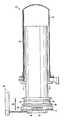
- FIG. 1is a side sectional view of a conventional vertical furnace having a silicon carbide liner and a boat assembly for holding semiconductor wafers residing therein;
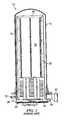
- FIG. 2is a side sectional view of the furnace with the boat assembly removed therefrom, and an exchange fixture according to the present invention coupled to and supporting the lower end of the liner prior to removal of the liner from the operating furnace;
- FIG. 3is a side sectional view of the liner being removed from a heated operating vertical furnace by the exchange fixture and the elevator;
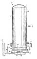
- FIG. 4is an exploded view of the exchange fixture with respect to the liner and the associated cap thereover;
- FIG. 5is a front view of the inner ring which is adapted to couple to and support the liner during lowering and elevation of the liner into the heated operating furnace;
- FIG. 6is a blown up view taken along lines 6 — 6 in FIG. 5;
- FIG. 7is a top view of the flanged inner ring depicting the top supporting surface adapted to support the liner;
- FIG. 8is a bottom view of the inner ring depicting the lower extending annular member and flange surface adapted to rest upon the low-friction ring and within the outer ring, as well as the two mounting threaded holes receiving the handles;
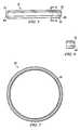
- FIG. 9is a front view of the low-friction ring, shown upside down, including the vertical annular interface and the annular flange interface each adapted to provide a low friction interface between the inner ring and the outer ring;
- FIG. 10is a top view of the low-friction ring
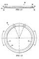
- FIG. 11is front view of the outer ring, which is adapted to encompass and receive the inner ring and low-friction ring such that the inner ring is easily rotatable therewithin;
- FIG. 12is a bottom view of the outer ring
- FIG. 13is a top view of one of the two handles coupled to the inner ring to permit rotation of the inner-ring with respect to the outer ring when heated and also when cooled;
- FIG. 14is a side view of the handle of FIG. 13 .
- FIG. 1there is generally shown at 10 a side sectional view of a vertical-type thermal processing furnace 10 .
- the thermal processing furnaceis designed to be compact and have a relatively small footprint.
- the furnaceis typically used to perform a variety of semi-conductor fabrication processes, including annealing, diffusion, oxidation and low and high pressure chemical vapor deposition (CVD).
- CVDchemical vapor deposition
- the thermal processing furnace 10includes a main outer housing or outer tube 12 .
- the vertical furnace 10includes a cylindrical process inner tube 14 that has an upper open end 16 and an opposed open end 18 .
- the process tube 14can be formed of any high temperature material such as alumina, silicon carbide, quartz, and other ceramic materials, and is preferably composed of silicon carbide or quartz.
- the main outer housing or outer tubeis surrounded by a suitable heating element (not shown), that uses resistance-heated elements or RF heated black body cavity susceptors as the primary heat source. This particular type of heat source is simple to implement, well characterized and widely accepted as a reliable technique for stable and uniform control of the furnace temperature.
- the heating elementscan be composed of low mask, high temperature metallic wires.
- the insulation surrounding the heating elementcan be composed of ceramic fibers of high insulation value and low thermal mass. All are designed for fast responses to temperature changes.
- the furnacecan also include an air cooling system to help cool the heating chamber if desired.
- the process tube diameter, and thus the size of the vertical furnace,can be easily scaled to accommodate wafers of varying sizes.
- a wafer boat 20is selectively disposed in the furnace 10 and is slotted to accommodate a selected number of semiconductor wafers when disposed within the inner tube compartment 22 . These wafers can be unprocessed or processed wafers.
- Ports 26 , 27 , 28 and 29provide various functions. Port 26 is the location for the inner thermocouple, which coupled with the spike thermocouples (not show) are responsible for temperature monitoring of the vertical furnace.
- Port 27is the manifold exhaust mouth from which all gases are exhausted out of the vertical furnace.
- Ports 28 and 29are the ports for the ultra-torr fittings, where the gas injectors are placed. The number and location of injector ports vary by process requirements and tool configuration.
- the heating elementis arranged about the outer tube 10 to heat the inside of the liner to a predetermined temperature, eg. 400° C. to 1200° C. in the case of low pressure chemical vapor deposition (LPCVD), or 800° C. to 1200° C. in the case of oxidation or diffusion.
- a control unit(not shown) is used to regulate the temperature of the liner 14 according to the exigencies of the processing technique.
- a temperature sensorsuch as an optical pyrometer can be used to sense the chamber temperature and can be linked to the control unit.
- the heating unitpreferably forms an isothermal heating zone within the liner 14 , as is known in the art. As shown in FIG.
- the wafer boat 20is supported by a heat insulating stanchion 24 .
- the bottom portion of the wafer support assemblyhas an integrally formed and radially outwardly extending flange plate, as shown, and is coupled to a boat elevator (not shown) for inserting and removing the wafer boat 20 within the liner 14 for processing.
- the wafer support assembly 20is thus selectively vertically movable along the vertical axis to selectively move the wafer support assembly into and out of the furnace heating chamber 22 .
- the liner 14will start to release particles that exceed processing limits established for the particular processing being performed on the semiconductor wafers.
- the entire furnaceis shut down, allowing the whole unit to cool before, removing and replacing the liner 14 .
- this entire shutdownis a considerable expense as many parts then need to be replaced and cleaned, and leads to a significant downtime of the furnace which reduces the efficiency of the entire processing since the furnace is offline for an extended period of time.
- an exchange fixtureadapted to permit the quick exchanging of the liner 14 within the operating vertical furnace.
- the furnaceremains fully operational at a temperature exceeding 500° C., and other components do not need to be replaced, such as the remaining quartzware and associated hardware.
- the films defined on the various interior parts that would otherwise be subject to stress fractures associated with film stressare maintained to allow for additional processing.
- the lineris not adapted to be removed from a heated furnace with any of the fixtures provided by the manufacturers.
- the present inventionpermits the exchange of the liner from an operating vertical furnace using a fixture adapted to perform this operation, and the careful control of the exchange by controlling the descent rate of the old liner from the operating furnace, and the ascent rate of the new liner into the operating vertical furnace at controlled speeds to avoid quick heating and quick cooling which could damage the liner and possibly other elements of the operating furnace.
- a fixture generally shown at 30is seen to be selectively coupled to the bottom of the liner 14 via a support ring 32 and secured thereto through, a selectable locking arrangement.
- the key components of liner 30include an inner ring 34 , a low friction ring 36 , preferably comprised of Teflon®, and an outer ring 38 , wherein the low friction ring 36 permits the rotation of the inner ring there within when heated or cooled as it supports the liner 14 .
- the fixture 30is raised by a support 41 of elevator 40 such that the lower ring 34 is coupled via the liner support ring 32 to the flanged bottom of liner 14 , as shown.
- the inner liner 34is then rotated by rotating handles 42 extending through a slot 44 defined in the outer ring 38 to lock the liner 14 into the steel manifold of the operating vertical furnace 10 .
- the liner 14is conventionally, supported by the liner support ring 32 , which is provided with tabs by the manufacture to lock and unlock the liner 14 upon rotation thereof to the steel manifold and inside of the outer tube 10 .
- the flanged low friction member 36which is structured to provide a two dimensional interface between the inner ring 34 and the outer ring 38 .
- the low friction ring 36is flanged such that it interfaces the horizontal arcuate surfaces of the inner ring 34 and the outer ring 38 as the inner ring 34 supported thereon, and importantly, interfaces the vertical arcuate surfaces of the inner ring outer surface and the outer ring inner surface.
- the interface of the inner ring outer walls and the outer ring inner wallis important due to the fact that when the fixture 30 is proximate to operating furnace 10 and hot liner 14 is removed from an operating heated furnace 10 , the exceeding high temperatures, typically being greater than 500° C., cause these rings to expand and otherwise would tend to bind due to the friction generated therebetween, even if the material of each ring is the same.
- the present inventionis adapted to allow the rotation and removal of the liner 14 when heated, which is not contemplated for by the manufacture of the furnace. A metal on metal surface would not be adequate and would tend to bind, especially with the tight tolerances that are maintained, and due to the significant weight of the liner 14 itself.
- FIG. 4there is shown an exploded view of the fixture 30 of the present invention including the inner ring 34 , the flanged Teflon® low-friction ring 36 , and the outer ring 38 .
- the support ring 32is not part of the fixture 30 , but is utilized with the fixture 30 to provide the interface between the liner 14 and the fixture 30 .
- the inner ring 34has a lower annular flanged portion 50 adapted to be supported upon the upper laterally extending flanged surface of the low friction ring 36 .
- the liner support 32is adapted to be supported on an annular top surface 52 of inner ring 34 and is sandwiched against the lower annular surface of liner 14 .
- a laterally extending flange 54 of low friction ring 36rests upon a top flanged surface 56 of outer ring 38 , and also has a downwardly extending portion 58 which is disposed between an outer annular surface 60 of the downwardly extending portion 62 of inner ring 34 and an inner annular surface 64 of the outer ring 38 .
- FIG. 5there is shown a front view of the inner ring 34 having the downwardly extending portion 62 , and the upper annular supporting surface 52 which is flanged and inwardly tapered to permit the friction fit coupling of the liner support ring 32 thereupon.
- the liner support ring 32is disposed upon this upper annular surface 52 and interfaces to the annular bottom surface of the liner 14 .
- the downwardly extending outer surface 60 of portion 62is securingly and coaxially received within the low friction ring 36 , such that a flange portion 64 extends over flange 54 of ring 36 , and the outer surface 60 extends within and securingly interfaces an inner surface 66 of ring 36 .
- FIG. 6there is shown in a blown up view of the flange 52 and the flange portion 64 previously described.
- FIG. 7there is shown a top view of the inner ring 34
- FIG. 8illustrates a bottom view of the inner ring 34
- FIG. 8there is further shown two sets of two threaded openings 66 that are adapted to permit the coupling of the respective handles 42 thereto to provide a leverage point and allow the rotation of the inner ring 34 within the,outer ring 38 as previously described.
- the arcuate separation of openings 66is approximately 14° to separate the torque points along the inner ring and prevent damage thereto.
- FIG. 11there is a front view of the low friction ring 36 , shown upside down from the assembled view in FIG. 2, FIG. 3, and the exploded view of FIG. 4 .
- the low friction ring 36is seen to have the flanged portion 54 and the arcuate sidewall portion 58 having an outer sidewall 70 .
- the thickness of the flanged portion 54is preferably 3 mm, and the thickness of the arcuate outer wall 58 is preferably 3 mm.
- These two surfaces 54 and 70each provide a low friction interface between the inner ring 34 and the outer ring 38 , especially when they are heated due to the operating temperature of the vertical furnace.
- FIG. 10illustrates a top view of the flanged low friction ring 36 , and which defines an opening 74 .
- FIG. 11there is shown a front view of the outer ring 38 having a radial flanged portion 80 and a vertical side wall portion 82 .
- the flanged portion 80defines the upper support surface 56 and the portion 82 defining a sidewall surface 84 .
- Also shown at 84is the notch cutout for placement of the handles, so that when the fixture 30 is assembled the bottom plane of the assembly is flat.
- the surface 56 and in inner annulas surface 64receive the downwardly positioned inner low-friction ring 36 , whereby annular member 62 is received therewithin.
- FIG. 12there is shown a bottom view of the outer ring 38 depicting the pair of arcuately extending slots 44 extending an arcuate distance A.
- the slots 44permit the extension of the radially extending handles 42 therethrough and therealong to permit the rotation of the inner ring 34 to allow the unlocking and locking of the liner 14 from the vertical furnace side wall 12 .
- this arcuate distanceis preferably 52.45°.
- FIG. 13there is shown a top view of one handle 42 having a pair of openings 90 permitting the extension of threaded fasteners (not shown) into the corresponding threaded recesses 66 of the inner ring bottom surface, as depicted in FIG. 8 .
- these openings 90are separated an arcuate distance of 14° to separate the torque moments along the rim of the inner ring 34 to prevent damage thereto.
- Handle 42is seen to have a “T-shape”, having laterally extending portions 92 , and an elongated radially extending portion 94 .
- Opening 96adapted to receive a tool to apply a moment of force thereat and thereby rotate the inner ring 34 within the outer ring 38 .
- Openings 90 and 96are intentionally designed to be spaced in a “T” arrangement, whereby the distance of the outer opening 96 is at least double the distance between the openings 90 .
- the openingis designed to allow a tool or handle to be inserted for additional leverage, if required.
- FIG. 14there is shown a side view of the handle 42 .
Landscapes
- Engineering & Computer Science (AREA)
- Mechanical Engineering (AREA)
- General Engineering & Computer Science (AREA)
Abstract
Description
The present invention is generally related to thermal processing furnaces for processing semiconductor wafers, and particularly to a vertical-type processing furnace including vertical nitride furnaces.
Thermal processing furnaces, also known as diffusion furnaces, have been widely known and used for many years to perform a variety of semiconductor fabrication processes, including annealing, diffusion, oxidation, and chemical vapor deposition (CVD). As a result, these processes are well understood, especially with regard to the impact of process variables on the quality and uniformity of resulting products.
Thermal processing furnaces typically employ either a horizontal-type furnace, or a vertical-tye furnace. For some applications, vertical-type furnaces are preferred because they create less particles during use, thus decreasing the incidence of contamination and wafer waste. In addition, they can be easily automated, and they require less floor space because of their relatively small footprint.
Both conventional types of diffusion furnaces are designed to heat semiconductor wafers to desired temperatures to promote either diffusion of the dopants to a desired depth while maintaining line width smaller than 1 micron, as known, or to perform other conventional processing techniques such as the application of an oxide layer to the wafer or deposition of a chemical vapor layer to the wafer. The heating requirements of the wafer during processing are known and well understood, and thus are closely monitored.
Conventional vertical-type thermal processing furnaces are designed to support the outer tube and inner tube within the furnace in the vertical position. The inner tube is conventionally referred to as a liner, and typical liners include silicon carbide liners which operate above 500° Celsius, such as in the TEL a-303i Vertical Nitride Furnace. Although the silicon carbide liners are designed to operate at temperatures above 500° Celsius, the current fixtures provided by manufactures for replacing the silicon carbide liners are designed for use at room temperature. Unfortunately, to achieve room temperature, the entire furnace must be inactivated and cooled, which is an exceptionally expensive process. Every time a furnace is brought offline to room temperature, numerous expensive parts need to be serviced and/or replaced before the vertical furnace can be heated again and brought back online. For instance, the inner thermalcouple (TC) needs to be replaced as it is usually contaminated with a nitride film which degrades operational properties and necessitates requalification. This part alone may cost $7,000.00, excluding labor. In addition, a stainless steel manifold and O ring needs to be replaced, which is usually contaminated with ammonia chloride. A fair estimate for bringing a vertical furnace offline and then again back online, such as to replace the silicon carbide liner may cost in excess of $30,000.00
A silicon carbide liner will eventually generate particles in excess of a maximum allowable particle count after a predetermined time, such as a thickness of 3.5 microns, and needs to be replaced. However, the entire furnace does not need to be retrofitted as often, but is conventionally brought offline to provide for the replacement of the silicon carbide liner since the removal fixtures are only designed by the manufacture to operate at room temperature.
Accordingly, there is a need to provide for the retrofitting of a silicon carbide liner within an operating heated vertical furnace, including the installation and removal of the liner from the operating heated semiconductor vertical furnace without causing damage to either the old or new liner, or the furnace itself. Such a solution would significantly reduce the overall operating cost of the vertical furnace by allowing the retrofitting of the silicon carbide liner itself without bringing the furnace offline.
The present invention achieves technical advantages as an liner exchange fixture having a low-friction member and method of operation adapted to permit the retrofitting of a silicon carbide liner in an operating heated semiconductor vertical furnace. The present invention includes an exchange fixture adapted to operate while heated, such as above 500° Celsius, and also at room temperature if desired. The exchange fixture can be maneuvered proximate the operating furnace to unlock the liner and lower the liner therefrom at a controlled descent rate to control the cooling rate of the liner from its normal operating temperature. The fixture is also adapted to insert a new liner into the operating furnace at a controlled rate such that the liner is brought up to an operating temperature at a controlled rate to prevent damage thereto. Thus, the film integrity on the remaining operating furnace parts are maintained.
In one preferred embodiment, the exchange fixture comprises an outer ring, and an inner ring residing within the outer ring and adapted to support the liner when elevated to the operating vertical furnace, and when the liner is removed and inserted from/into the operating vertical furnace. The inner ring includes structure adapted to facilitate rotation of the inner ring between a locked position when the liner is elevated in the operating vertical furnace, and an unlocked position when the liner is to be lowered from the operating vertical furnace. Advantageously, the low-friction member is flanged and interposed between and interfacing the inner ring and the outer ring along 2 surfaces, thus facilitating the ease of rotation of the inner ring within the outer ring when the inner ring is both heated proximate the furnace and when lowered from the operating vertical furnace, including at room temperature. This low-friction member accommodates the expansion and contraction of the inner ring within the outer ring due to the heating and cooling cycles of the inner ring when disposed proximate the furnace or when removing the liner from the operating furnace.
An elevator is adapted to support the outer ring for lowering the liner from the operating furnace, and also for elevating the exchange fixture such that the liner is raised into the operating furnace. The first ring includes at least one handle, and preferably two opposing handles, adapted to facilitate rotation of the inner ring within the outer ring along the low friction member when the liner is positioned in the operating vertical furnace.
Each handle has at least two securing points coupled to the inner ring, wherein each handle is uniquely secured at two securing points separated a predetermined actuate distance from one another. Each handle has a lever point radially separated from the inner ring along an axis extending between the two securing points to form a “T” relationship relative to the two securing points.
Advantageously, the elevator is adapted to lower the fixture and the supported old liner from the operating furnace at a rate below a predetermined maximum rate to control the rate of temperature decrease of the liner when removed from the operating vertical furnace. Likewise, the elevator is also adapted to elevate the new liner into the operating vertical furnace at a rate below a predetermined maximum rate to control the rate of temperature increase of the liner when inserted into the operating vertical furnace. This controlled ascent and descent rate prevents damage to the old and new liner as it is cooled or brought up to operating temperature.
FIG. 1 is a side sectional view of a conventional vertical furnace having a silicon carbide liner and a boat assembly for holding semiconductor wafers residing therein;
FIG. 2 is a side sectional view of the furnace with the boat assembly removed therefrom, and an exchange fixture according to the present invention coupled to and supporting the lower end of the liner prior to removal of the liner from the operating furnace;
FIG. 3 is a side sectional view of the liner being removed from a heated operating vertical furnace by the exchange fixture and the elevator;
FIG. 4 is an exploded view of the exchange fixture with respect to the liner and the associated cap thereover;
FIG. 5 is a front view of the inner ring which is adapted to couple to and support the liner during lowering and elevation of the liner into the heated operating furnace;
FIG. 6 is a blown up view taken alonglines 6—6 in FIG. 5;
FIG. 7 is a top view of the flanged inner ring depicting the top supporting surface adapted to support the liner;
FIG. 8 is a bottom view of the inner ring depicting the lower extending annular member and flange surface adapted to rest upon the low-friction ring and within the outer ring, as well as the two mounting threaded holes receiving the handles;
FIG. 9 is a front view of the low-friction ring, shown upside down, including the vertical annular interface and the annular flange interface each adapted to provide a low friction interface between the inner ring and the outer ring;
FIG. 10 is a top view of the low-friction ring;
FIG. 11 is front view of the outer ring, which is adapted to encompass and receive the inner ring and low-friction ring such that the inner ring is easily rotatable therewithin;
FIG. 12 is a bottom view of the outer ring;
FIG. 13 is a top view of one of the two handles coupled to the inner ring to permit rotation of the inner-ring with respect to the outer ring when heated and also when cooled; and
FIG. 14 is a side view of the handle of FIG.13.
Referring now to FIG. 1, there is generally shown at10 a side sectional view of a vertical-typethermal processing furnace 10. The thermal processing furnace is designed to be compact and have a relatively small footprint. The furnace is typically used to perform a variety of semi-conductor fabrication processes, including annealing, diffusion, oxidation and low and high pressure chemical vapor deposition (CVD).
Thethermal processing furnace 10 includes a main outer housing orouter tube 12. Thevertical furnace 10 includes a cylindrical processinner tube 14 that has an upperopen end 16 and an opposedopen end 18. Theprocess tube 14 can be formed of any high temperature material such as alumina, silicon carbide, quartz, and other ceramic materials, and is preferably composed of silicon carbide or quartz. The main outer housing or outer tube is surrounded by a suitable heating element (not shown), that uses resistance-heated elements or RF heated black body cavity susceptors as the primary heat source. This particular type of heat source is simple to implement, well characterized and widely accepted as a reliable technique for stable and uniform control of the furnace temperature. The heating elements can be composed of low mask, high temperature metallic wires. The insulation surrounding the heating element can be composed of ceramic fibers of high insulation value and low thermal mass. All are designed for fast responses to temperature changes. The furnace can also include an air cooling system to help cool the heating chamber if desired. The process tube diameter, and thus the size of the vertical furnace, can be easily scaled to accommodate wafers of varying sizes. As shown in FIG. 1, awafer boat 20 is selectively disposed in thefurnace 10 and is slotted to accommodate a selected number of semiconductor wafers when disposed within the inner tube compartment22. These wafers can be unprocessed or processed wafers.Ports Port 26 is the location for the inner thermocouple, which coupled with the spike thermocouples (not show) are responsible for temperature monitoring of the vertical furnace.Port 27 is the manifold exhaust mouth from which all gases are exhausted out of the vertical furnace.Ports
The heating element is arranged about theouter tube 10 to heat the inside of the liner to a predetermined temperature, eg. 400° C. to 1200° C. in the case of low pressure chemical vapor deposition (LPCVD), or 800° C. to 1200° C. in the case of oxidation or diffusion. A control unit (not shown) is used to regulate the temperature of theliner 14 according to the exigencies of the processing technique. For example, according to one practice, a temperature sensor, such as an optical pyrometer can be used to sense the chamber temperature and can be linked to the control unit. The heating unit preferably forms an isothermal heating zone within theliner 14, as is known in the art. As shown in FIG. 1, thewafer boat 20 is supported by aheat insulating stanchion 24. The bottom portion of the wafer support assembly has an integrally formed and radially outwardly extending flange plate, as shown, and is coupled to a boat elevator (not shown) for inserting and removing thewafer boat 20 within theliner 14 for processing. Thewafer support assembly 20 is thus selectively vertically movable along the vertical axis to selectively move the wafer support assembly into and out of the furnace heating chamber22.
After an extended operating time, theliner 14 will start to release particles that exceed processing limits established for the particular processing being performed on the semiconductor wafers. Conventionally, the entire furnace is shut down, allowing the whole unit to cool before, removing and replacing theliner 14. As previously mentioned in the Background of the Invention, this entire shutdown is a considerable expense as many parts then need to be replaced and cleaned, and leads to a significant downtime of the furnace which reduces the efficiency of the entire processing since the furnace is offline for an extended period of time.
Referring now to FIG. 2, according to the present invention, there is provided an exchange fixture adapted to permit the quick exchanging of theliner 14 within the operating vertical furnace. Advantageously, the furnace remains fully operational at a temperature exceeding 500° C., and other components do not need to be replaced, such as the remaining quartzware and associated hardware. Specifically, by maintaining the furnace operating temperature the films defined on the various interior parts that would otherwise be subject to stress fractures associated with film stress are maintained to allow for additional processing.
Again, conventionally, the liner is not adapted to be removed from a heated furnace with any of the fixtures provided by the manufacturers. The present invention permits the exchange of the liner from an operating vertical furnace using a fixture adapted to perform this operation, and the careful control of the exchange by controlling the descent rate of the old liner from the operating furnace, and the ascent rate of the new liner into the operating vertical furnace at controlled speeds to avoid quick heating and quick cooling which could damage the liner and possibly other elements of the operating furnace.
As shown in FIG. 3, a fixture generally shown at30 according to the present invention is seen to be selectively coupled to the bottom of theliner 14 via asupport ring 32 and secured thereto through, a selectable locking arrangement. The key components ofliner 30 include aninner ring 34, alow friction ring 36, preferably comprised of Teflon®, and anouter ring 38, wherein thelow friction ring 36 permits the rotation of the inner ring there within when heated or cooled as it supports theliner 14. When it is desired to exchange theliner 14 from the operatingfurnace 10, thefixture 30 is raised by asupport 41 ofelevator 40 such that thelower ring 34 is coupled via theliner support ring 32 to the flanged bottom ofliner 14, as shown. Theinner liner 34 is then rotated by rotatinghandles 42 extending through aslot 44 defined in theouter ring 38 to lock theliner 14 into the steel manifold of the operatingvertical furnace 10. Specifically, theliner 14 is conventionally, supported by theliner support ring 32, which is provided with tabs by the manufacture to lock and unlock theliner 14 upon rotation thereof to the steel manifold and inside of theouter tube 10.
One technical feature of the present invention is the inclusion of the flangedlow friction member 36 which is structured to provide a two dimensional interface between theinner ring 34 and theouter ring 38. Specifically, thelow friction ring 36 is flanged such that it interfaces the horizontal arcuate surfaces of theinner ring 34 and theouter ring 38 as theinner ring 34 supported thereon, and importantly, interfaces the vertical arcuate surfaces of the inner ring outer surface and the outer ring inner surface. The interface of the inner ring outer walls and the outer ring inner wall is important due to the fact that when thefixture 30 is proximate to operatingfurnace 10 andhot liner 14 is removed from an operatingheated furnace 10, the exceeding high temperatures, typically being greater than 500° C., cause these rings to expand and otherwise would tend to bind due to the friction generated therebetween, even if the material of each ring is the same. The present invention is adapted to allow the rotation and removal of theliner 14 when heated, which is not contemplated for by the manufacture of the furnace. A metal on metal surface would not be adequate and would tend to bind, especially with the tight tolerances that are maintained, and due to the significant weight of theliner 14 itself.
Referring now to FIG. 4, there is shown an exploded view of thefixture 30 of the present invention including theinner ring 34, the flanged Teflon® low-friction ring 36, and theouter ring 38. Thesupport ring 32 is not part of thefixture 30, but is utilized with thefixture 30 to provide the interface between theliner 14 and thefixture 30. As can be appreciated in FIG. 4, theinner ring 34 has a lower annularflanged portion 50 adapted to be supported upon the upper laterally extending flanged surface of thelow friction ring 36. Theliner support 32 is adapted to be supported on an annulartop surface 52 ofinner ring 34 and is sandwiched against the lower annular surface ofliner 14. As shown, a laterally extendingflange 54 oflow friction ring 36 rests upon a topflanged surface 56 ofouter ring 38, and also has a downwardly extendingportion 58 which is disposed between an outerannular surface 60 of the downwardly extendingportion 62 ofinner ring 34 and an innerannular surface 64 of theouter ring 38.
Referring now to FIG. 5, there is shown a front view of theinner ring 34 having the downwardly extendingportion 62, and the upperannular supporting surface 52 which is flanged and inwardly tapered to permit the friction fit coupling of theliner support ring 32 thereupon. During use theliner support ring 32 is disposed upon this upperannular surface 52 and interfaces to the annular bottom surface of theliner 14. The downwardly extendingouter surface 60 ofportion 62 is securingly and coaxially received within thelow friction ring 36, such that aflange portion 64 extends overflange 54 ofring 36, and theouter surface 60 extends within and securingly interfaces aninner surface 66 ofring 36.
Referring to FIG. 6, there is shown in a blown up view of theflange 52 and theflange portion 64 previously described.
Referring to FIG. 7, there is shown a top view of theinner ring 34, and FIG. 8 illustrates a bottom view of theinner ring 34. In FIG. 8, there is further shown two sets of two threadedopenings 66 that are adapted to permit the coupling of therespective handles 42 thereto to provide a leverage point and allow the rotation of theinner ring 34 within the,outer ring 38 as previously described. The arcuate separation ofopenings 66 is approximately 14° to separate the torque points along the inner ring and prevent damage thereto.
Referring now to FIG. 11, there is a front view of thelow friction ring 36, shown upside down from the assembled view in FIG. 2, FIG. 3, and the exploded view of FIG.4. Thelow friction ring 36 is seen to have theflanged portion 54 and thearcuate sidewall portion 58 having anouter sidewall 70. The thickness of theflanged portion 54 is preferably 3 mm, and the thickness of the arcuateouter wall 58 is preferably 3 mm. These twosurfaces inner ring 34 and theouter ring 38, especially when they are heated due to the operating temperature of the vertical furnace.
FIG. 10 illustrates a top view of the flangedlow friction ring 36, and which defines anopening 74.
Referring now to FIG. 11, there is shown a front view of theouter ring 38 having a radialflanged portion 80 and a verticalside wall portion 82. Theflanged portion 80 defines theupper support surface 56 and theportion 82 defining a sidewall surface84. Also shown at84 is the notch cutout for placement of the handles, so that when thefixture 30 is assembled the bottom plane of the assembly is flat. As depicted in FIG. 11, thesurface 56 and in inner annulas surface64 receive the downwardly positioned inner low-friction ring 36, wherebyannular member 62 is received therewithin.
Referring now to FIG. 12 there is shown a bottom view of theouter ring 38 depicting the pair of arcuately extendingslots 44 extending an arcuate distance A. As shown and discussed with regards to FIG.2 and FIG. 3, theslots 44 permit the extension of theradially extending handles 42 therethrough and therealong to permit the rotation of theinner ring 34 to allow the unlocking and locking of theliner 14 from the verticalfurnace side wall 12. Preferably, this arcuate distance is preferably 52.45°.
Referring now to FIG. 13, there is shown a top view of onehandle 42 having a pair ofopenings 90 permitting the extension of threaded fasteners (not shown) into the corresponding threadedrecesses 66 of the inner ring bottom surface, as depicted in FIG.8. Preferably, theseopenings 90 are separated an arcuate distance of 14° to separate the torque moments along the rim of theinner ring 34 to prevent damage thereto.Handle 42 is seen to have a “T-shape”, having laterally extendingportions 92, and an elongated radially extendingportion 94. Defined at the distal end ofarm 94 is anopening 96 adapted to receive a tool to apply a moment of force thereat and thereby rotate theinner ring 34 within theouter ring 38.Openings outer opening 96 is at least double the distance between theopenings 90. The opening is designed to allow a tool or handle to be inserted for additional leverage, if required.
Referring to FIG. 14, there is shown a side view of thehandle 42.
Though the invention has been described with respect to a specific preferred embodiment, many variations and modifications will become apparent to those skilled in the art upon reading the present application. It is therefore the intention that the appended claims be interpreted as broadly as possible in view of the prior art to include all such variations and modifications. For instance, with a slight modification, the outer ring could be designed to support the liner and rotate with respect to the inner ring whereby the elevator would support the inner ring.
Claims (13)
1. A fixture adapted to install and remove a liner in an operating heated vertically extending semiconductor furnace, comprising:
a first ring;
a second ring coupled to the first ring and adapted to support the liner when elevated into the operating furnace, and when the liner is removed from the furnace, the second ring having structure adapted to rotate the second ring between a locked position when the liner is elevated into the operating furnace and an unlocked position when the liner is lowered from the operating furnace; and
a low-friction member interfaced between the first ring and the second ring facilitating the rotation of the second ring with respect to the first ring when the second ring is both heated proximate the furnace and when lowered from the furnace.
2. The fixture as specified inclaim 1 wherein the first ring is an outer ring, and the second ring is an inner ring.
3. The fixture as specified inclaim 1 wherein the inner ring at least partially resides in the outer ring.
4. The fixture as specified inclaim 1 further comprising an elevator adapted to support the fixture and elevate the liner into the operating furnace, and lower the liner from the operating furnace.
5. The fixture as specified inclaim 4 wherein the second ring further comprises at least one radially extending handle adapted to facilitate rotation of the second ring with respect to the first ring along the low-friction member.
6. The fixture as specified inclaim 5 wherein the handles have at least two securing points coupling the handles to the second ring, the two securing points being separated a predetermined arcuate distance.
7. The fixture as specified inclaim 6 wherein the handles each have a lever point radially separated from the second ring along an axis extending between the two securing points to form a “T” relationship relative to the two securing points.
8. The fixture as specified inclaim 7 wherein the two securing points are separated an arcuate distance of at least 14 degrees.
9. The fixture as specified inclaim 4 wherein the elevator is adapted to lower the liner from the heated operating furnace at a rate below a predetermined maximum rate to control the rate of temperature change of the hot liner when removed from the heated furnace.
10. The fixture as specified inclaim 4 wherein the elevator is adapted to elevate the liner into the heated operating furnace at a rate below a predetermined maximum rate to control the rate of temperature change of the liner when inserted into the heated furnace.
11. The fixture as specified inclaim 9 wherein the predetermined maximum rate is 50 mm/min.
12. The fixture as specified inclaim 10 wherein the predetermined maximum rate is 50 mm/min.
13. The fixture as specified inclaim 1 wherein the low-friction member has a flanged rim extending over the first ring.
Priority Applications (2)
| Application Number | Priority Date | Filing Date | Title |
|---|---|---|---|
| US10/337,150US6692249B1 (en) | 2003-01-06 | 2003-01-06 | Hot liner insertion/removal fixture |
| US10/754,521US7195479B2 (en) | 2003-01-06 | 2004-01-08 | Hot liner insertion/removal fixture |
Applications Claiming Priority (1)
| Application Number | Priority Date | Filing Date | Title |
|---|---|---|---|
| US10/337,150US6692249B1 (en) | 2003-01-06 | 2003-01-06 | Hot liner insertion/removal fixture |
Related Child Applications (1)
| Application Number | Title | Priority Date | Filing Date |
|---|---|---|---|
| US10/754,521DivisionUS7195479B2 (en) | 2003-01-06 | 2004-01-08 | Hot liner insertion/removal fixture |
Publications (1)
| Publication Number | Publication Date |
|---|---|
| US6692249B1true US6692249B1 (en) | 2004-02-17 |
Family
ID=31188235
Family Applications (2)
| Application Number | Title | Priority Date | Filing Date |
|---|---|---|---|
| US10/337,150Expired - LifetimeUS6692249B1 (en) | 2003-01-06 | 2003-01-06 | Hot liner insertion/removal fixture |
| US10/754,521Expired - LifetimeUS7195479B2 (en) | 2003-01-06 | 2004-01-08 | Hot liner insertion/removal fixture |
Family Applications After (1)
| Application Number | Title | Priority Date | Filing Date |
|---|---|---|---|
| US10/754,521Expired - LifetimeUS7195479B2 (en) | 2003-01-06 | 2004-01-08 | Hot liner insertion/removal fixture |
Country Status (1)
| Country | Link |
|---|---|
| US (2) | US6692249B1 (en) |
Cited By (8)
| Publication number | Priority date | Publication date | Assignee | Title |
|---|---|---|---|---|
| US20040146827A1 (en)* | 2003-01-06 | 2004-07-29 | Beatty James Hoyt | Hot liner insertion/removal fixture |
| US20040226518A1 (en)* | 2003-02-27 | 2004-11-18 | Asahi Glass Company, Limited | Outer tube made of silicon carbide and thermal treatment system for semiconductors |
| US20070231757A1 (en)* | 2006-03-29 | 2007-10-04 | Tokyo Electron Limited | Thermal processing furnace, gas delivery system therefor, and methods for delivering a process gas thereto |
| US20070238313A1 (en)* | 2006-03-30 | 2007-10-11 | Tokyo Electron Limited | Method for replacing a nitrous oxide based oxidation process with a nitric oxide based oxidation process for substrate processing |
| US20080242109A1 (en)* | 2007-03-30 | 2008-10-02 | Tokyo Electron Limited | Method for growing a thin oxynitride film on a substrate |
| US20090035463A1 (en)* | 2007-08-03 | 2009-02-05 | Tokyo Electron Limited | Thermal processing system and method for forming an oxide layer on substrates |
| US20090088000A1 (en)* | 2007-09-30 | 2009-04-02 | Tokyo Electron Limited | Method for growing an oxynitride film on a substrate |
| WO2010039570A3 (en)* | 2008-09-30 | 2010-11-18 | Hemlock Semiconductor Corporation | Method of determining an amount of impurities that a contaminating material contributes to high purity silicon and furnace for treating high purity silicon |
Families Citing this family (303)
| Publication number | Priority date | Publication date | Assignee | Title |
|---|---|---|---|---|
| USD588079S1 (en)* | 2006-06-16 | 2009-03-10 | Tokyo Electron Limited | Heat dissipation deterrence link for semiconductor manufacture |
| TWD122891S1 (en)* | 2006-06-16 | 2008-05-11 | 東京威力科創股份有限公司 | Heat Suppression Ring for Semiconductor Manufacturing |
| US20110209693A1 (en)* | 2007-08-06 | 2011-09-01 | Teoss Co., Ltd., | silicon heating furnace |
| US9157150B2 (en)* | 2007-12-04 | 2015-10-13 | Cypress Semiconductor Corporation | Method of operating a processing chamber used in forming electronic devices |
| US9394608B2 (en) | 2009-04-06 | 2016-07-19 | Asm America, Inc. | Semiconductor processing reactor and components thereof |
| US8802201B2 (en) | 2009-08-14 | 2014-08-12 | Asm America, Inc. | Systems and methods for thin-film deposition of metal oxides using excited nitrogen-oxygen species |
| US20130023129A1 (en) | 2011-07-20 | 2013-01-24 | Asm America, Inc. | Pressure transmitter for a semiconductor processing environment |
| WO2013021454A1 (en) | 2011-08-09 | 2013-02-14 | 東横化学株式会社 | Heat treatment device |
| US9017481B1 (en) | 2011-10-28 | 2015-04-28 | Asm America, Inc. | Process feed management for semiconductor substrate processing |
| US10714315B2 (en) | 2012-10-12 | 2020-07-14 | Asm Ip Holdings B.V. | Semiconductor reaction chamber showerhead |
| US20160376700A1 (en) | 2013-02-01 | 2016-12-29 | Asm Ip Holding B.V. | System for treatment of deposition reactor |
| US11015245B2 (en) | 2014-03-19 | 2021-05-25 | Asm Ip Holding B.V. | Gas-phase reactor and system having exhaust plenum and components thereof |
| US10858737B2 (en) | 2014-07-28 | 2020-12-08 | Asm Ip Holding B.V. | Showerhead assembly and components thereof |
| US9890456B2 (en) | 2014-08-21 | 2018-02-13 | Asm Ip Holding B.V. | Method and system for in situ formation of gas-phase compounds |
| US10941490B2 (en) | 2014-10-07 | 2021-03-09 | Asm Ip Holding B.V. | Multiple temperature range susceptor, assembly, reactor and system including the susceptor, and methods of using the same |
| US10276355B2 (en) | 2015-03-12 | 2019-04-30 | Asm Ip Holding B.V. | Multi-zone reactor, system including the reactor, and method of using the same |
| US10458018B2 (en) | 2015-06-26 | 2019-10-29 | Asm Ip Holding B.V. | Structures including metal carbide material, devices including the structures, and methods of forming same |
| US10211308B2 (en) | 2015-10-21 | 2019-02-19 | Asm Ip Holding B.V. | NbMC layers |
| US11139308B2 (en) | 2015-12-29 | 2021-10-05 | Asm Ip Holding B.V. | Atomic layer deposition of III-V compounds to form V-NAND devices |
| US10529554B2 (en) | 2016-02-19 | 2020-01-07 | Asm Ip Holding B.V. | Method for forming silicon nitride film selectively on sidewalls or flat surfaces of trenches |
| US10343920B2 (en) | 2016-03-18 | 2019-07-09 | Asm Ip Holding B.V. | Aligned carbon nanotubes |
| US10190213B2 (en) | 2016-04-21 | 2019-01-29 | Asm Ip Holding B.V. | Deposition of metal borides |
| US10865475B2 (en) | 2016-04-21 | 2020-12-15 | Asm Ip Holding B.V. | Deposition of metal borides and silicides |
| US10367080B2 (en) | 2016-05-02 | 2019-07-30 | Asm Ip Holding B.V. | Method of forming a germanium oxynitride film |
| US11453943B2 (en) | 2016-05-25 | 2022-09-27 | Asm Ip Holding B.V. | Method for forming carbon-containing silicon/metal oxide or nitride film by ALD using silicon precursor and hydrocarbon precursor |
| US10612137B2 (en) | 2016-07-08 | 2020-04-07 | Asm Ip Holdings B.V. | Organic reactants for atomic layer deposition |
| US9859151B1 (en) | 2016-07-08 | 2018-01-02 | Asm Ip Holding B.V. | Selective film deposition method to form air gaps |
| US9887082B1 (en) | 2016-07-28 | 2018-02-06 | Asm Ip Holding B.V. | Method and apparatus for filling a gap |
| US9812320B1 (en) | 2016-07-28 | 2017-11-07 | Asm Ip Holding B.V. | Method and apparatus for filling a gap |
| KR102532607B1 (en) | 2016-07-28 | 2023-05-15 | 에이에스엠 아이피 홀딩 비.브이. | Substrate processing apparatus and method of operating the same |
| US10643826B2 (en) | 2016-10-26 | 2020-05-05 | Asm Ip Holdings B.V. | Methods for thermally calibrating reaction chambers |
| US11532757B2 (en) | 2016-10-27 | 2022-12-20 | Asm Ip Holding B.V. | Deposition of charge trapping layers |
| US10714350B2 (en) | 2016-11-01 | 2020-07-14 | ASM IP Holdings, B.V. | Methods for forming a transition metal niobium nitride film on a substrate by atomic layer deposition and related semiconductor device structures |
| US10229833B2 (en) | 2016-11-01 | 2019-03-12 | Asm Ip Holding B.V. | Methods for forming a transition metal nitride film on a substrate by atomic layer deposition and related semiconductor device structures |
| KR102546317B1 (en) | 2016-11-15 | 2023-06-21 | 에이에스엠 아이피 홀딩 비.브이. | Gas supply unit and substrate processing apparatus including the same |
| KR102762543B1 (en) | 2016-12-14 | 2025-02-05 | 에이에스엠 아이피 홀딩 비.브이. | Substrate processing apparatus |
| US11581186B2 (en) | 2016-12-15 | 2023-02-14 | Asm Ip Holding B.V. | Sequential infiltration synthesis apparatus |
| US11447861B2 (en) | 2016-12-15 | 2022-09-20 | Asm Ip Holding B.V. | Sequential infiltration synthesis apparatus and a method of forming a patterned structure |
| KR102700194B1 (en) | 2016-12-19 | 2024-08-28 | 에이에스엠 아이피 홀딩 비.브이. | Substrate processing apparatus |
| US10269558B2 (en) | 2016-12-22 | 2019-04-23 | Asm Ip Holding B.V. | Method of forming a structure on a substrate |
| US10867788B2 (en) | 2016-12-28 | 2020-12-15 | Asm Ip Holding B.V. | Method of forming a structure on a substrate |
| US11390950B2 (en) | 2017-01-10 | 2022-07-19 | Asm Ip Holding B.V. | Reactor system and method to reduce residue buildup during a film deposition process |
| US10468261B2 (en) | 2017-02-15 | 2019-11-05 | Asm Ip Holding B.V. | Methods for forming a metallic film on a substrate by cyclical deposition and related semiconductor device structures |
| US10529563B2 (en) | 2017-03-29 | 2020-01-07 | Asm Ip Holdings B.V. | Method for forming doped metal oxide films on a substrate by cyclical deposition and related semiconductor device structures |
| KR102457289B1 (en) | 2017-04-25 | 2022-10-21 | 에이에스엠 아이피 홀딩 비.브이. | Method for depositing a thin film and manufacturing a semiconductor device |
| US10892156B2 (en) | 2017-05-08 | 2021-01-12 | Asm Ip Holding B.V. | Methods for forming a silicon nitride film on a substrate and related semiconductor device structures |
| US10770286B2 (en) | 2017-05-08 | 2020-09-08 | Asm Ip Holdings B.V. | Methods for selectively forming a silicon nitride film on a substrate and related semiconductor device structures |
| US10886123B2 (en) | 2017-06-02 | 2021-01-05 | Asm Ip Holding B.V. | Methods for forming low temperature semiconductor layers and related semiconductor device structures |
| US12040200B2 (en) | 2017-06-20 | 2024-07-16 | Asm Ip Holding B.V. | Semiconductor processing apparatus and methods for calibrating a semiconductor processing apparatus |
| US11306395B2 (en) | 2017-06-28 | 2022-04-19 | Asm Ip Holding B.V. | Methods for depositing a transition metal nitride film on a substrate by atomic layer deposition and related deposition apparatus |
| KR20190009245A (en) | 2017-07-18 | 2019-01-28 | 에이에스엠 아이피 홀딩 비.브이. | Methods for forming a semiconductor device structure and related semiconductor device structures |
| US11374112B2 (en) | 2017-07-19 | 2022-06-28 | Asm Ip Holding B.V. | Method for depositing a group IV semiconductor and related semiconductor device structures |
| US10541333B2 (en) | 2017-07-19 | 2020-01-21 | Asm Ip Holding B.V. | Method for depositing a group IV semiconductor and related semiconductor device structures |
| US11018002B2 (en) | 2017-07-19 | 2021-05-25 | Asm Ip Holding B.V. | Method for selectively depositing a Group IV semiconductor and related semiconductor device structures |
| US10590535B2 (en) | 2017-07-26 | 2020-03-17 | Asm Ip Holdings B.V. | Chemical treatment, deposition and/or infiltration apparatus and method for using the same |
| TWI815813B (en) | 2017-08-04 | 2023-09-21 | 荷蘭商Asm智慧財產控股公司 | Showerhead assembly for distributing a gas within a reaction chamber |
| US10770336B2 (en) | 2017-08-08 | 2020-09-08 | Asm Ip Holding B.V. | Substrate lift mechanism and reactor including same |
| US10692741B2 (en) | 2017-08-08 | 2020-06-23 | Asm Ip Holdings B.V. | Radiation shield |
| US11139191B2 (en) | 2017-08-09 | 2021-10-05 | Asm Ip Holding B.V. | Storage apparatus for storing cassettes for substrates and processing apparatus equipped therewith |
| US11769682B2 (en) | 2017-08-09 | 2023-09-26 | Asm Ip Holding B.V. | Storage apparatus for storing cassettes for substrates and processing apparatus equipped therewith |
| US11830730B2 (en) | 2017-08-29 | 2023-11-28 | Asm Ip Holding B.V. | Layer forming method and apparatus |
| KR102491945B1 (en) | 2017-08-30 | 2023-01-26 | 에이에스엠 아이피 홀딩 비.브이. | Substrate processing apparatus |
| US11295980B2 (en) | 2017-08-30 | 2022-04-05 | Asm Ip Holding B.V. | Methods for depositing a molybdenum metal film over a dielectric surface of a substrate by a cyclical deposition process and related semiconductor device structures |
| US11056344B2 (en) | 2017-08-30 | 2021-07-06 | Asm Ip Holding B.V. | Layer forming method |
| KR102401446B1 (en) | 2017-08-31 | 2022-05-24 | 에이에스엠 아이피 홀딩 비.브이. | Substrate processing apparatus |
| KR102630301B1 (en) | 2017-09-21 | 2024-01-29 | 에이에스엠 아이피 홀딩 비.브이. | Method of sequential infiltration synthesis treatment of infiltrateable material and structures and devices formed using same |
| US10844484B2 (en) | 2017-09-22 | 2020-11-24 | Asm Ip Holding B.V. | Apparatus for dispensing a vapor phase reactant to a reaction chamber and related methods |
| US10658205B2 (en) | 2017-09-28 | 2020-05-19 | Asm Ip Holdings B.V. | Chemical dispensing apparatus and methods for dispensing a chemical to a reaction chamber |
| US10403504B2 (en) | 2017-10-05 | 2019-09-03 | Asm Ip Holding B.V. | Method for selectively depositing a metallic film on a substrate |
| US10923344B2 (en) | 2017-10-30 | 2021-02-16 | Asm Ip Holding B.V. | Methods for forming a semiconductor structure and related semiconductor structures |
| US10910262B2 (en) | 2017-11-16 | 2021-02-02 | Asm Ip Holding B.V. | Method of selectively depositing a capping layer structure on a semiconductor device structure |
| US11022879B2 (en) | 2017-11-24 | 2021-06-01 | Asm Ip Holding B.V. | Method of forming an enhanced unexposed photoresist layer |
| CN111344522B (en) | 2017-11-27 | 2022-04-12 | 阿斯莫Ip控股公司 | Including clean mini-environment device |
| WO2019103613A1 (en) | 2017-11-27 | 2019-05-31 | Asm Ip Holding B.V. | A storage device for storing wafer cassettes for use with a batch furnace |
| US10872771B2 (en) | 2018-01-16 | 2020-12-22 | Asm Ip Holding B. V. | Method for depositing a material film on a substrate within a reaction chamber by a cyclical deposition process and related device structures |
| TWI799494B (en) | 2018-01-19 | 2023-04-21 | 荷蘭商Asm 智慧財產控股公司 | Deposition method |
| KR102695659B1 (en) | 2018-01-19 | 2024-08-14 | 에이에스엠 아이피 홀딩 비.브이. | Method for depositing a gap filling layer by plasma assisted deposition |
| US11018047B2 (en) | 2018-01-25 | 2021-05-25 | Asm Ip Holding B.V. | Hybrid lift pin |
| USD880437S1 (en) | 2018-02-01 | 2020-04-07 | Asm Ip Holding B.V. | Gas supply plate for semiconductor manufacturing apparatus |
| US11081345B2 (en) | 2018-02-06 | 2021-08-03 | Asm Ip Holding B.V. | Method of post-deposition treatment for silicon oxide film |
| US10896820B2 (en) | 2018-02-14 | 2021-01-19 | Asm Ip Holding B.V. | Method for depositing a ruthenium-containing film on a substrate by a cyclical deposition process |
| WO2019158960A1 (en) | 2018-02-14 | 2019-08-22 | Asm Ip Holding B.V. | A method for depositing a ruthenium-containing film on a substrate by a cyclical deposition process |
| US10731249B2 (en) | 2018-02-15 | 2020-08-04 | Asm Ip Holding B.V. | Method of forming a transition metal containing film on a substrate by a cyclical deposition process, a method for supplying a transition metal halide compound to a reaction chamber, and related vapor deposition apparatus |
| KR102636427B1 (en) | 2018-02-20 | 2024-02-13 | 에이에스엠 아이피 홀딩 비.브이. | Substrate processing method and apparatus |
| US10975470B2 (en) | 2018-02-23 | 2021-04-13 | Asm Ip Holding B.V. | Apparatus for detecting or monitoring for a chemical precursor in a high temperature environment |
| US11473195B2 (en) | 2018-03-01 | 2022-10-18 | Asm Ip Holding B.V. | Semiconductor processing apparatus and a method for processing a substrate |
| US11629406B2 (en) | 2018-03-09 | 2023-04-18 | Asm Ip Holding B.V. | Semiconductor processing apparatus comprising one or more pyrometers for measuring a temperature of a substrate during transfer of the substrate |
| US11114283B2 (en) | 2018-03-16 | 2021-09-07 | Asm Ip Holding B.V. | Reactor, system including the reactor, and methods of manufacturing and using same |
| KR102646467B1 (en) | 2018-03-27 | 2024-03-11 | 에이에스엠 아이피 홀딩 비.브이. | Method of forming an electrode on a substrate and a semiconductor device structure including an electrode |
| US11088002B2 (en) | 2018-03-29 | 2021-08-10 | Asm Ip Holding B.V. | Substrate rack and a substrate processing system and method |
| US11230766B2 (en) | 2018-03-29 | 2022-01-25 | Asm Ip Holding B.V. | Substrate processing apparatus and method |
| KR102501472B1 (en) | 2018-03-30 | 2023-02-20 | 에이에스엠 아이피 홀딩 비.브이. | Substrate processing method |
| KR102600229B1 (en) | 2018-04-09 | 2023-11-10 | 에이에스엠 아이피 홀딩 비.브이. | Substrate supporting device, substrate processing apparatus including the same and substrate processing method |
| JP7122856B2 (en)* | 2018-05-02 | 2022-08-22 | 東京エレクトロン株式会社 | Heat treatment equipment |
| US12025484B2 (en) | 2018-05-08 | 2024-07-02 | Asm Ip Holding B.V. | Thin film forming method |
| TWI811348B (en) | 2018-05-08 | 2023-08-11 | 荷蘭商Asm 智慧財產控股公司 | Methods for depositing an oxide film on a substrate by a cyclical deposition process and related device structures |
| US12272527B2 (en) | 2018-05-09 | 2025-04-08 | Asm Ip Holding B.V. | Apparatus for use with hydrogen radicals and method of using same |
| KR20190129718A (en) | 2018-05-11 | 2019-11-20 | 에이에스엠 아이피 홀딩 비.브이. | Methods for forming a doped metal carbide film on a substrate and related semiconductor device structures |
| KR102596988B1 (en) | 2018-05-28 | 2023-10-31 | 에이에스엠 아이피 홀딩 비.브이. | Method of processing a substrate and a device manufactured by the same |
| TWI840362B (en) | 2018-06-04 | 2024-05-01 | 荷蘭商Asm Ip私人控股有限公司 | Wafer handling chamber with moisture reduction |
| US11718913B2 (en) | 2018-06-04 | 2023-08-08 | Asm Ip Holding B.V. | Gas distribution system and reactor system including same |
| US11286562B2 (en) | 2018-06-08 | 2022-03-29 | Asm Ip Holding B.V. | Gas-phase chemical reactor and method of using same |
| KR102568797B1 (en) | 2018-06-21 | 2023-08-21 | 에이에스엠 아이피 홀딩 비.브이. | Substrate processing system |
| US10797133B2 (en) | 2018-06-21 | 2020-10-06 | Asm Ip Holding B.V. | Method for depositing a phosphorus doped silicon arsenide film and related semiconductor device structures |
| KR102854019B1 (en) | 2018-06-27 | 2025-09-02 | 에이에스엠 아이피 홀딩 비.브이. | Periodic deposition method for forming a metal-containing material and films and structures comprising the metal-containing material |
| TWI873894B (en) | 2018-06-27 | 2025-02-21 | 荷蘭商Asm Ip私人控股有限公司 | Cyclic deposition methods for forming metal-containing material and films and structures including the metal-containing material |
| US10612136B2 (en) | 2018-06-29 | 2020-04-07 | ASM IP Holding, B.V. | Temperature-controlled flange and reactor system including same |
| KR102686758B1 (en) | 2018-06-29 | 2024-07-18 | 에이에스엠 아이피 홀딩 비.브이. | Method for depositing a thin film and manufacturing a semiconductor device |
| US10388513B1 (en) | 2018-07-03 | 2019-08-20 | Asm Ip Holding B.V. | Method for depositing silicon-free carbon-containing film as gap-fill layer by pulse plasma-assisted deposition |
| US10755922B2 (en) | 2018-07-03 | 2020-08-25 | Asm Ip Holding B.V. | Method for depositing silicon-free carbon-containing film as gap-fill layer by pulse plasma-assisted deposition |
| US10767789B2 (en) | 2018-07-16 | 2020-09-08 | Asm Ip Holding B.V. | Diaphragm valves, valve components, and methods for forming valve components |
| US11053591B2 (en) | 2018-08-06 | 2021-07-06 | Asm Ip Holding B.V. | Multi-port gas injection system and reactor system including same |
| US10883175B2 (en) | 2018-08-09 | 2021-01-05 | Asm Ip Holding B.V. | Vertical furnace for processing substrates and a liner for use therein |
| US10829852B2 (en) | 2018-08-16 | 2020-11-10 | Asm Ip Holding B.V. | Gas distribution device for a wafer processing apparatus |
| US11430674B2 (en) | 2018-08-22 | 2022-08-30 | Asm Ip Holding B.V. | Sensor array, apparatus for dispensing a vapor phase reactant to a reaction chamber and related methods |
| US11024523B2 (en) | 2018-09-11 | 2021-06-01 | Asm Ip Holding B.V. | Substrate processing apparatus and method |
| KR102707956B1 (en) | 2018-09-11 | 2024-09-19 | 에이에스엠 아이피 홀딩 비.브이. | Method for deposition of a thin film |
| US11049751B2 (en) | 2018-09-14 | 2021-06-29 | Asm Ip Holding B.V. | Cassette supply system to store and handle cassettes and processing apparatus equipped therewith |
| CN110970344B (en) | 2018-10-01 | 2024-10-25 | Asmip控股有限公司 | Substrate holding apparatus, system comprising the same and method of using the same |
| US11232963B2 (en) | 2018-10-03 | 2022-01-25 | Asm Ip Holding B.V. | Substrate processing apparatus and method |
| KR102592699B1 (en) | 2018-10-08 | 2023-10-23 | 에이에스엠 아이피 홀딩 비.브이. | Substrate support unit and apparatuses for depositing thin film and processing the substrate including the same |
| KR102546322B1 (en) | 2018-10-19 | 2023-06-21 | 에이에스엠 아이피 홀딩 비.브이. | Substrate processing apparatus and substrate processing method |
| KR102605121B1 (en) | 2018-10-19 | 2023-11-23 | 에이에스엠 아이피 홀딩 비.브이. | Substrate processing apparatus and substrate processing method |
| USD948463S1 (en) | 2018-10-24 | 2022-04-12 | Asm Ip Holding B.V. | Susceptor for semiconductor substrate supporting apparatus |
| US12378665B2 (en) | 2018-10-26 | 2025-08-05 | Asm Ip Holding B.V. | High temperature coatings for a preclean and etch apparatus and related methods |
| US11087997B2 (en) | 2018-10-31 | 2021-08-10 | Asm Ip Holding B.V. | Substrate processing apparatus for processing substrates |
| KR102748291B1 (en) | 2018-11-02 | 2024-12-31 | 에이에스엠 아이피 홀딩 비.브이. | Substrate support unit and substrate processing apparatus including the same |
| US11572620B2 (en) | 2018-11-06 | 2023-02-07 | Asm Ip Holding B.V. | Methods for selectively depositing an amorphous silicon film on a substrate |
| US11031242B2 (en) | 2018-11-07 | 2021-06-08 | Asm Ip Holding B.V. | Methods for depositing a boron doped silicon germanium film |
| US10818758B2 (en) | 2018-11-16 | 2020-10-27 | Asm Ip Holding B.V. | Methods for forming a metal silicate film on a substrate in a reaction chamber and related semiconductor device structures |
| US10847366B2 (en) | 2018-11-16 | 2020-11-24 | Asm Ip Holding B.V. | Methods for depositing a transition metal chalcogenide film on a substrate by a cyclical deposition process |
| US12040199B2 (en) | 2018-11-28 | 2024-07-16 | Asm Ip Holding B.V. | Substrate processing apparatus for processing substrates |
| US11217444B2 (en) | 2018-11-30 | 2022-01-04 | Asm Ip Holding B.V. | Method for forming an ultraviolet radiation responsive metal oxide-containing film |
| KR102636428B1 (en) | 2018-12-04 | 2024-02-13 | 에이에스엠 아이피 홀딩 비.브이. | A method for cleaning a substrate processing apparatus |
| US11158513B2 (en) | 2018-12-13 | 2021-10-26 | Asm Ip Holding B.V. | Methods for forming a rhenium-containing film on a substrate by a cyclical deposition process and related semiconductor device structures |
| TWI874340B (en) | 2018-12-14 | 2025-03-01 | 荷蘭商Asm Ip私人控股有限公司 | Method of forming device structure, structure formed by the method and system for performing the method |
| TWI866480B (en) | 2019-01-17 | 2024-12-11 | 荷蘭商Asm Ip 私人控股有限公司 | Methods of forming a transition metal containing film on a substrate by a cyclical deposition process |
| KR102727227B1 (en) | 2019-01-22 | 2024-11-07 | 에이에스엠 아이피 홀딩 비.브이. | Semiconductor processing device |
| CN111524788B (en) | 2019-02-01 | 2023-11-24 | Asm Ip私人控股有限公司 | Method for forming topologically selective films of silicon oxide |
| TWI873122B (en) | 2019-02-20 | 2025-02-21 | 荷蘭商Asm Ip私人控股有限公司 | Method of filling a recess formed within a surface of a substrate, semiconductor structure formed according to the method, and semiconductor processing apparatus |
| TWI838458B (en) | 2019-02-20 | 2024-04-11 | 荷蘭商Asm Ip私人控股有限公司 | Apparatus and methods for plug fill deposition in 3-d nand applications |
| TWI845607B (en) | 2019-02-20 | 2024-06-21 | 荷蘭商Asm Ip私人控股有限公司 | Cyclical deposition method and apparatus for filling a recess formed within a substrate surface |
| KR102626263B1 (en) | 2019-02-20 | 2024-01-16 | 에이에스엠 아이피 홀딩 비.브이. | Cyclical deposition method including treatment step and apparatus for same |
| TWI842826B (en) | 2019-02-22 | 2024-05-21 | 荷蘭商Asm Ip私人控股有限公司 | Substrate processing apparatus and method for processing substrate |
| KR102782593B1 (en) | 2019-03-08 | 2025-03-14 | 에이에스엠 아이피 홀딩 비.브이. | Structure Including SiOC Layer and Method of Forming Same |
| KR102858005B1 (en) | 2019-03-08 | 2025-09-09 | 에이에스엠 아이피 홀딩 비.브이. | Method for Selective Deposition of Silicon Nitride Layer and Structure Including Selectively-Deposited Silicon Nitride Layer |
| US11742198B2 (en) | 2019-03-08 | 2023-08-29 | Asm Ip Holding B.V. | Structure including SiOCN layer and method of forming same |
| JP2020167398A (en) | 2019-03-28 | 2020-10-08 | エーエスエム・アイピー・ホールディング・ベー・フェー | Door openers and substrate processing equipment provided with door openers |
| KR102809999B1 (en) | 2019-04-01 | 2025-05-19 | 에이에스엠 아이피 홀딩 비.브이. | Method of manufacturing semiconductor device |
| KR20200123380A (en) | 2019-04-19 | 2020-10-29 | 에이에스엠 아이피 홀딩 비.브이. | Layer forming method and apparatus |
| KR20200125453A (en) | 2019-04-24 | 2020-11-04 | 에이에스엠 아이피 홀딩 비.브이. | Gas-phase reactor system and method of using same |
| KR20200130121A (en) | 2019-05-07 | 2020-11-18 | 에이에스엠 아이피 홀딩 비.브이. | Chemical source vessel with dip tube |
| US11289326B2 (en) | 2019-05-07 | 2022-03-29 | Asm Ip Holding B.V. | Method for reforming amorphous carbon polymer film |
| KR20200130652A (en) | 2019-05-10 | 2020-11-19 | 에이에스엠 아이피 홀딩 비.브이. | Method of depositing material onto a surface and structure formed according to the method |
| JP7598201B2 (en) | 2019-05-16 | 2024-12-11 | エーエスエム・アイピー・ホールディング・ベー・フェー | Wafer boat handling apparatus, vertical batch furnace and method |
| JP7612342B2 (en) | 2019-05-16 | 2025-01-14 | エーエスエム・アイピー・ホールディング・ベー・フェー | Wafer boat handling apparatus, vertical batch furnace and method |
| USD975665S1 (en) | 2019-05-17 | 2023-01-17 | Asm Ip Holding B.V. | Susceptor shaft |
| USD947913S1 (en) | 2019-05-17 | 2022-04-05 | Asm Ip Holding B.V. | Susceptor shaft |
| USD935572S1 (en) | 2019-05-24 | 2021-11-09 | Asm Ip Holding B.V. | Gas channel plate |
| USD922229S1 (en) | 2019-06-05 | 2021-06-15 | Asm Ip Holding B.V. | Device for controlling a temperature of a gas supply unit |
| KR20200141002A (en) | 2019-06-06 | 2020-12-17 | 에이에스엠 아이피 홀딩 비.브이. | Method of using a gas-phase reactor system including analyzing exhausted gas |
| KR20200141931A (en) | 2019-06-10 | 2020-12-21 | 에이에스엠 아이피 홀딩 비.브이. | Method for cleaning quartz epitaxial chambers |
| KR20200143254A (en) | 2019-06-11 | 2020-12-23 | 에이에스엠 아이피 홀딩 비.브이. | Method of forming an electronic structure using an reforming gas, system for performing the method, and structure formed using the method |
| USD944946S1 (en) | 2019-06-14 | 2022-03-01 | Asm Ip Holding B.V. | Shower plate |
| USD931978S1 (en) | 2019-06-27 | 2021-09-28 | Asm Ip Holding B.V. | Showerhead vacuum transport |
| KR20210005515A (en) | 2019-07-03 | 2021-01-14 | 에이에스엠 아이피 홀딩 비.브이. | Temperature control assembly for substrate processing apparatus and method of using same |
| JP7499079B2 (en) | 2019-07-09 | 2024-06-13 | エーエスエム・アイピー・ホールディング・ベー・フェー | Plasma device using coaxial waveguide and substrate processing method |
| CN112216646A (en) | 2019-07-10 | 2021-01-12 | Asm Ip私人控股有限公司 | Substrate supporting assembly and substrate processing device comprising same |
| KR20210010307A (en) | 2019-07-16 | 2021-01-27 | 에이에스엠 아이피 홀딩 비.브이. | Substrate processing apparatus |
| KR20210010816A (en) | 2019-07-17 | 2021-01-28 | 에이에스엠 아이피 홀딩 비.브이. | Radical assist ignition plasma system and method |
| KR102860110B1 (en) | 2019-07-17 | 2025-09-16 | 에이에스엠 아이피 홀딩 비.브이. | Methods of forming silicon germanium structures |
| US11643724B2 (en) | 2019-07-18 | 2023-05-09 | Asm Ip Holding B.V. | Method of forming structures using a neutral beam |
| TWI839544B (en) | 2019-07-19 | 2024-04-21 | 荷蘭商Asm Ip私人控股有限公司 | Method of forming topology-controlled amorphous carbon polymer film |
| KR20210010817A (en) | 2019-07-19 | 2021-01-28 | 에이에스엠 아이피 홀딩 비.브이. | Method of Forming Topology-Controlled Amorphous Carbon Polymer Film |
| TWI851767B (en) | 2019-07-29 | 2024-08-11 | 荷蘭商Asm Ip私人控股有限公司 | Methods for selective deposition utilizing n-type dopants and/or alternative dopants to achieve high dopant incorporation |
| CN112309900A (en) | 2019-07-30 | 2021-02-02 | Asm Ip私人控股有限公司 | Substrate processing apparatus |
| CN112309899A (en) | 2019-07-30 | 2021-02-02 | Asm Ip私人控股有限公司 | Substrate processing apparatus |
| US12169361B2 (en) | 2019-07-30 | 2024-12-17 | Asm Ip Holding B.V. | Substrate processing apparatus and method |
| US11587814B2 (en) | 2019-07-31 | 2023-02-21 | Asm Ip Holding B.V. | Vertical batch furnace assembly |
| US11587815B2 (en) | 2019-07-31 | 2023-02-21 | Asm Ip Holding B.V. | Vertical batch furnace assembly |
| US11227782B2 (en) | 2019-07-31 | 2022-01-18 | Asm Ip Holding B.V. | Vertical batch furnace assembly |
| CN112323048B (en) | 2019-08-05 | 2024-02-09 | Asm Ip私人控股有限公司 | Liquid level sensor for chemical source container |
| CN112342526A (en) | 2019-08-09 | 2021-02-09 | Asm Ip私人控股有限公司 | Heater assembly including cooling device and method of using same |
| USD965044S1 (en) | 2019-08-19 | 2022-09-27 | Asm Ip Holding B.V. | Susceptor shaft |
| USD965524S1 (en) | 2019-08-19 | 2022-10-04 | Asm Ip Holding B.V. | Susceptor support |
| JP2021031769A (en) | 2019-08-21 | 2021-03-01 | エーエスエム アイピー ホールディング ビー.ブイ. | Production apparatus of mixed gas of film deposition raw material and film deposition apparatus |
| KR20210024423A (en) | 2019-08-22 | 2021-03-05 | 에이에스엠 아이피 홀딩 비.브이. | Method for forming a structure with a hole |
| USD930782S1 (en) | 2019-08-22 | 2021-09-14 | Asm Ip Holding B.V. | Gas distributor |
| USD940837S1 (en) | 2019-08-22 | 2022-01-11 | Asm Ip Holding B.V. | Electrode |
| USD949319S1 (en) | 2019-08-22 | 2022-04-19 | Asm Ip Holding B.V. | Exhaust duct |
| USD979506S1 (en) | 2019-08-22 | 2023-02-28 | Asm Ip Holding B.V. | Insulator |
| KR20210024420A (en) | 2019-08-23 | 2021-03-05 | 에이에스엠 아이피 홀딩 비.브이. | Method for depositing silicon oxide film having improved quality by peald using bis(diethylamino)silane |
| US11286558B2 (en) | 2019-08-23 | 2022-03-29 | Asm Ip Holding B.V. | Methods for depositing a molybdenum nitride film on a surface of a substrate by a cyclical deposition process and related semiconductor device structures including a molybdenum nitride film |
| KR102806450B1 (en) | 2019-09-04 | 2025-05-12 | 에이에스엠 아이피 홀딩 비.브이. | Methods for selective deposition using a sacrificial capping layer |
| KR102733104B1 (en) | 2019-09-05 | 2024-11-22 | 에이에스엠 아이피 홀딩 비.브이. | Substrate processing apparatus |
| US11562901B2 (en) | 2019-09-25 | 2023-01-24 | Asm Ip Holding B.V. | Substrate processing method |
| CN112593212B (en) | 2019-10-02 | 2023-12-22 | Asm Ip私人控股有限公司 | Method for forming topologically selective silicon oxide film by cyclic plasma enhanced deposition process |
| TWI846953B (en) | 2019-10-08 | 2024-07-01 | 荷蘭商Asm Ip私人控股有限公司 | Substrate processing device |
| TW202128273A (en) | 2019-10-08 | 2021-08-01 | 荷蘭商Asm Ip私人控股有限公司 | Gas injection system, reactor system, and method of depositing material on surface of substratewithin reaction chamber |
| KR20210042810A (en) | 2019-10-08 | 2021-04-20 | 에이에스엠 아이피 홀딩 비.브이. | Reactor system including a gas distribution assembly for use with activated species and method of using same |
| TWI846966B (en) | 2019-10-10 | 2024-07-01 | 荷蘭商Asm Ip私人控股有限公司 | Method of forming a photoresist underlayer and structure including same |
| US12009241B2 (en) | 2019-10-14 | 2024-06-11 | Asm Ip Holding B.V. | Vertical batch furnace assembly with detector to detect cassette |
| TWI834919B (en) | 2019-10-16 | 2024-03-11 | 荷蘭商Asm Ip私人控股有限公司 | Method of topology-selective film formation of silicon oxide |
| US11637014B2 (en) | 2019-10-17 | 2023-04-25 | Asm Ip Holding B.V. | Methods for selective deposition of doped semiconductor material |
| KR102845724B1 (en) | 2019-10-21 | 2025-08-13 | 에이에스엠 아이피 홀딩 비.브이. | Apparatus and methods for selectively etching films |
| KR20210050453A (en) | 2019-10-25 | 2021-05-07 | 에이에스엠 아이피 홀딩 비.브이. | Methods for filling a gap feature on a substrate surface and related semiconductor structures |
| US11646205B2 (en) | 2019-10-29 | 2023-05-09 | Asm Ip Holding B.V. | Methods of selectively forming n-type doped material on a surface, systems for selectively forming n-type doped material, and structures formed using same |
| KR20210054983A (en) | 2019-11-05 | 2021-05-14 | 에이에스엠 아이피 홀딩 비.브이. | Structures with doped semiconductor layers and methods and systems for forming same |
| US11501968B2 (en) | 2019-11-15 | 2022-11-15 | Asm Ip Holding B.V. | Method for providing a semiconductor device with silicon filled gaps |
| KR102861314B1 (en) | 2019-11-20 | 2025-09-17 | 에이에스엠 아이피 홀딩 비.브이. | Method of depositing carbon-containing material on a surface of a substrate, structure formed using the method, and system for forming the structure |
| US11450529B2 (en) | 2019-11-26 | 2022-09-20 | Asm Ip Holding B.V. | Methods for selectively forming a target film on a substrate comprising a first dielectric surface and a second metallic surface |
| CN112951697B (en) | 2019-11-26 | 2025-07-29 | Asmip私人控股有限公司 | Substrate processing apparatus |
| CN112885692B (en) | 2019-11-29 | 2025-08-15 | Asmip私人控股有限公司 | Substrate processing apparatus |
| CN120432376A (en) | 2019-11-29 | 2025-08-05 | Asm Ip私人控股有限公司 | Substrate processing apparatus |
| JP7527928B2 (en) | 2019-12-02 | 2024-08-05 | エーエスエム・アイピー・ホールディング・ベー・フェー | Substrate processing apparatus and substrate processing method |
| KR20210070898A (en) | 2019-12-04 | 2021-06-15 | 에이에스엠 아이피 홀딩 비.브이. | Substrate processing apparatus |
| KR20210078405A (en) | 2019-12-17 | 2021-06-28 | 에이에스엠 아이피 홀딩 비.브이. | Method of forming vanadium nitride layer and structure including the vanadium nitride layer |
| KR20210080214A (en) | 2019-12-19 | 2021-06-30 | 에이에스엠 아이피 홀딩 비.브이. | Methods for filling a gap feature on a substrate and related semiconductor structures |
| JP7636892B2 (en) | 2020-01-06 | 2025-02-27 | エーエスエム・アイピー・ホールディング・ベー・フェー | Channeled Lift Pins |
| JP7730637B2 (en) | 2020-01-06 | 2025-08-28 | エーエスエム・アイピー・ホールディング・ベー・フェー | Gas delivery assembly, components thereof, and reactor system including same |
| US11993847B2 (en) | 2020-01-08 | 2024-05-28 | Asm Ip Holding B.V. | Injector |
| KR20210093163A (en) | 2020-01-16 | 2021-07-27 | 에이에스엠 아이피 홀딩 비.브이. | Method of forming high aspect ratio features |
| KR102675856B1 (en) | 2020-01-20 | 2024-06-17 | 에이에스엠 아이피 홀딩 비.브이. | Method of forming thin film and method of modifying surface of thin film |
| TWI889744B (en) | 2020-01-29 | 2025-07-11 | 荷蘭商Asm Ip私人控股有限公司 | Contaminant trap system, and baffle plate stack |
| TW202513845A (en) | 2020-02-03 | 2025-04-01 | 荷蘭商Asm Ip私人控股有限公司 | Semiconductor structures and methods for forming the same |
| KR20210100010A (en) | 2020-02-04 | 2021-08-13 | 에이에스엠 아이피 홀딩 비.브이. | Method and apparatus for transmittance measurements of large articles |
| US11776846B2 (en) | 2020-02-07 | 2023-10-03 | Asm Ip Holding B.V. | Methods for depositing gap filling fluids and related systems and devices |
| TW202146691A (en) | 2020-02-13 | 2021-12-16 | 荷蘭商Asm Ip私人控股有限公司 | Gas distribution assembly, shower plate assembly, and method of adjusting conductance of gas to reaction chamber |
| KR20210103956A (en) | 2020-02-13 | 2021-08-24 | 에이에스엠 아이피 홀딩 비.브이. | Substrate processing apparatus including light receiving device and calibration method of light receiving device |
| TWI855223B (en) | 2020-02-17 | 2024-09-11 | 荷蘭商Asm Ip私人控股有限公司 | Method for growing phosphorous-doped silicon layer |
| CN113410160A (en) | 2020-02-28 | 2021-09-17 | Asm Ip私人控股有限公司 | System specially used for cleaning parts |
| KR20210113043A (en) | 2020-03-04 | 2021-09-15 | 에이에스엠 아이피 홀딩 비.브이. | Alignment fixture for a reactor system |
| KR20210116240A (en) | 2020-03-11 | 2021-09-27 | 에이에스엠 아이피 홀딩 비.브이. | Substrate handling device with adjustable joints |
| US11876356B2 (en) | 2020-03-11 | 2024-01-16 | Asm Ip Holding B.V. | Lockout tagout assembly and system and method of using same |
| KR102775390B1 (en) | 2020-03-12 | 2025-02-28 | 에이에스엠 아이피 홀딩 비.브이. | Method for Fabricating Layer Structure Having Target Topological Profile |
| US12173404B2 (en) | 2020-03-17 | 2024-12-24 | Asm Ip Holding B.V. | Method of depositing epitaxial material, structure formed using the method, and system for performing the method |
| KR102755229B1 (en) | 2020-04-02 | 2025-01-14 | 에이에스엠 아이피 홀딩 비.브이. | Thin film forming method |
| TWI887376B (en) | 2020-04-03 | 2025-06-21 | 荷蘭商Asm Ip私人控股有限公司 | Method for manufacturing semiconductor device |
| TWI888525B (en) | 2020-04-08 | 2025-07-01 | 荷蘭商Asm Ip私人控股有限公司 | Apparatus and methods for selectively etching silcon oxide films |
| US11821078B2 (en) | 2020-04-15 | 2023-11-21 | Asm Ip Holding B.V. | Method for forming precoat film and method for forming silicon-containing film |
| KR20210128343A (en) | 2020-04-15 | 2021-10-26 | 에이에스엠 아이피 홀딩 비.브이. | Method of forming chromium nitride layer and structure including the chromium nitride layer |
| US11996289B2 (en) | 2020-04-16 | 2024-05-28 | Asm Ip Holding B.V. | Methods of forming structures including silicon germanium and silicon layers, devices formed using the methods, and systems for performing the methods |
| KR20210130646A (en) | 2020-04-21 | 2021-11-01 | 에이에스엠 아이피 홀딩 비.브이. | Method for processing a substrate |
| KR20210132612A (en) | 2020-04-24 | 2021-11-04 | 에이에스엠 아이피 홀딩 비.브이. | Methods and apparatus for stabilizing vanadium compounds |
| KR20210132600A (en) | 2020-04-24 | 2021-11-04 | 에이에스엠 아이피 홀딩 비.브이. | Methods and systems for depositing a layer comprising vanadium, nitrogen, and a further element |
| CN113555279A (en) | 2020-04-24 | 2021-10-26 | Asm Ip私人控股有限公司 | Methods of forming vanadium nitride-containing layers and structures comprising the same |
| KR102866804B1 (en) | 2020-04-24 | 2025-09-30 | 에이에스엠 아이피 홀딩 비.브이. | Vertical batch furnace assembly comprising a cooling gas supply |
| TW202208671A (en) | 2020-04-24 | 2022-03-01 | 荷蘭商Asm Ip私人控股有限公司 | Methods of forming structures including vanadium boride and vanadium phosphide layers |
| KR102783898B1 (en) | 2020-04-29 | 2025-03-18 | 에이에스엠 아이피 홀딩 비.브이. | Solid source precursor vessel |
| KR20210134869A (en) | 2020-05-01 | 2021-11-11 | 에이에스엠 아이피 홀딩 비.브이. | Fast FOUP swapping with a FOUP handler |
| JP7726664B2 (en) | 2020-05-04 | 2025-08-20 | エーエスエム・アイピー・ホールディング・ベー・フェー | Substrate processing system for processing a substrate |
| KR102788543B1 (en) | 2020-05-13 | 2025-03-27 | 에이에스엠 아이피 홀딩 비.브이. | Laser alignment fixture for a reactor system |
| TW202146699A (en) | 2020-05-15 | 2021-12-16 | 荷蘭商Asm Ip私人控股有限公司 | Method of forming a silicon germanium layer, semiconductor structure, semiconductor device, method of forming a deposition layer, and deposition system |
| KR20210143653A (en) | 2020-05-19 | 2021-11-29 | 에이에스엠 아이피 홀딩 비.브이. | Substrate processing apparatus |
| KR102795476B1 (en) | 2020-05-21 | 2025-04-11 | 에이에스엠 아이피 홀딩 비.브이. | Structures including multiple carbon layers and methods of forming and using same |
| KR20210145079A (en) | 2020-05-21 | 2021-12-01 | 에이에스엠 아이피 홀딩 비.브이. | Flange and apparatus for processing substrates |
| TWI873343B (en) | 2020-05-22 | 2025-02-21 | 荷蘭商Asm Ip私人控股有限公司 | Reaction system for forming thin film on substrate |
| KR20210146802A (en) | 2020-05-26 | 2021-12-06 | 에이에스엠 아이피 홀딩 비.브이. | Method for depositing boron and gallium containing silicon germanium layers |
| TWI876048B (en) | 2020-05-29 | 2025-03-11 | 荷蘭商Asm Ip私人控股有限公司 | Substrate processing device |
| TW202212620A (en) | 2020-06-02 | 2022-04-01 | 荷蘭商Asm Ip私人控股有限公司 | Apparatus for processing substrate, method of forming film, and method of controlling apparatus for processing substrate |
| TW202208659A (en) | 2020-06-16 | 2022-03-01 | 荷蘭商Asm Ip私人控股有限公司 | Method for depositing boron containing silicon germanium layers |
| TW202218133A (en) | 2020-06-24 | 2022-05-01 | 荷蘭商Asm Ip私人控股有限公司 | Method for forming a layer provided with silicon |
| TWI873359B (en) | 2020-06-30 | 2025-02-21 | 荷蘭商Asm Ip私人控股有限公司 | Substrate processing method |
| US12431354B2 (en) | 2020-07-01 | 2025-09-30 | Asm Ip Holding B.V. | Silicon nitride and silicon oxide deposition methods using fluorine inhibitor |
| TW202202649A (en) | 2020-07-08 | 2022-01-16 | 荷蘭商Asm Ip私人控股有限公司 | Substrate processing method |
| KR20220010438A (en) | 2020-07-17 | 2022-01-25 | 에이에스엠 아이피 홀딩 비.브이. | Structures and methods for use in photolithography |
| KR20220011092A (en) | 2020-07-20 | 2022-01-27 | 에이에스엠 아이피 홀딩 비.브이. | Method and system for forming structures including transition metal layers |
| TWI878570B (en) | 2020-07-20 | 2025-04-01 | 荷蘭商Asm Ip私人控股有限公司 | Method and system for depositing molybdenum layers |
| US12322591B2 (en) | 2020-07-27 | 2025-06-03 | Asm Ip Holding B.V. | Thin film deposition process |
| KR20220021863A (en) | 2020-08-14 | 2022-02-22 | 에이에스엠 아이피 홀딩 비.브이. | Method for processing a substrate |
| US12040177B2 (en) | 2020-08-18 | 2024-07-16 | Asm Ip Holding B.V. | Methods for forming a laminate film by cyclical plasma-enhanced deposition processes |
| TW202228863A (en) | 2020-08-25 | 2022-08-01 | 荷蘭商Asm Ip私人控股有限公司 | Method for cleaning a substrate, method for selectively depositing, and reaction system |
| US11725280B2 (en) | 2020-08-26 | 2023-08-15 | Asm Ip Holding B.V. | Method for forming metal silicon oxide and metal silicon oxynitride layers |
| TW202229601A (en) | 2020-08-27 | 2022-08-01 | 荷蘭商Asm Ip私人控股有限公司 | Method of forming patterned structures, method of manipulating mechanical property, device structure, and substrate processing system |
| TW202217045A (en) | 2020-09-10 | 2022-05-01 | 荷蘭商Asm Ip私人控股有限公司 | Methods for depositing gap filing fluids and related systems and devices |
| USD990534S1 (en) | 2020-09-11 | 2023-06-27 | Asm Ip Holding B.V. | Weighted lift pin |
| KR20220036866A (en) | 2020-09-16 | 2022-03-23 | 에이에스엠 아이피 홀딩 비.브이. | Silicon oxide deposition method |
| USD1012873S1 (en) | 2020-09-24 | 2024-01-30 | Asm Ip Holding B.V. | Electrode for semiconductor processing apparatus |
| TWI889903B (en) | 2020-09-25 | 2025-07-11 | 荷蘭商Asm Ip私人控股有限公司 | Semiconductor processing method |
| US12009224B2 (en) | 2020-09-29 | 2024-06-11 | Asm Ip Holding B.V. | Apparatus and method for etching metal nitrides |
| KR20220045900A (en) | 2020-10-06 | 2022-04-13 | 에이에스엠 아이피 홀딩 비.브이. | Deposition method and an apparatus for depositing a silicon-containing material |
| CN114293174A (en) | 2020-10-07 | 2022-04-08 | Asm Ip私人控股有限公司 | Gas supply unit and substrate processing apparatus including the same |
| TW202229613A (en) | 2020-10-14 | 2022-08-01 | 荷蘭商Asm Ip私人控股有限公司 | Method of depositing material on stepped structure |
| TW202232565A (en) | 2020-10-15 | 2022-08-16 | 荷蘭商Asm Ip私人控股有限公司 | Method of manufacturing semiconductor device, and substrate treatment apparatus using ether-cat |
| TW202217037A (en) | 2020-10-22 | 2022-05-01 | 荷蘭商Asm Ip私人控股有限公司 | Method of depositing vanadium metal, structure, device and a deposition assembly |
| TW202223136A (en) | 2020-10-28 | 2022-06-16 | 荷蘭商Asm Ip私人控股有限公司 | Method for forming layer on substrate, and semiconductor processing system |
| TW202229620A (en) | 2020-11-12 | 2022-08-01 | 特文特大學 | Deposition system, method for controlling reaction condition, method for depositing |
| TW202229795A (en) | 2020-11-23 | 2022-08-01 | 荷蘭商Asm Ip私人控股有限公司 | A substrate processing apparatus with an injector |
| TW202235649A (en) | 2020-11-24 | 2022-09-16 | 荷蘭商Asm Ip私人控股有限公司 | Methods for filling a gap and related systems and devices |
| TW202235675A (en) | 2020-11-30 | 2022-09-16 | 荷蘭商Asm Ip私人控股有限公司 | Injector, and substrate processing apparatus |
| US12255053B2 (en) | 2020-12-10 | 2025-03-18 | Asm Ip Holding B.V. | Methods and systems for depositing a layer |
| TW202233884A (en) | 2020-12-14 | 2022-09-01 | 荷蘭商Asm Ip私人控股有限公司 | Method of forming structures for threshold voltage control |
| US11946137B2 (en) | 2020-12-16 | 2024-04-02 | Asm Ip Holding B.V. | Runout and wobble measurement fixtures |
| TW202232639A (en) | 2020-12-18 | 2022-08-16 | 荷蘭商Asm Ip私人控股有限公司 | Wafer processing apparatus with a rotatable table |
| TW202226899A (en) | 2020-12-22 | 2022-07-01 | 荷蘭商Asm Ip私人控股有限公司 | Plasma treatment device having matching box |
| TW202231903A (en) | 2020-12-22 | 2022-08-16 | 荷蘭商Asm Ip私人控股有限公司 | Transition metal deposition method, transition metal layer, and deposition assembly for depositing transition metal on substrate |
| TW202242184A (en) | 2020-12-22 | 2022-11-01 | 荷蘭商Asm Ip私人控股有限公司 | Precursor capsule, precursor vessel, vapor deposition assembly, and method of loading solid precursor into precursor vessel |
| USD980813S1 (en) | 2021-05-11 | 2023-03-14 | Asm Ip Holding B.V. | Gas flow control plate for substrate processing apparatus |
| USD1023959S1 (en) | 2021-05-11 | 2024-04-23 | Asm Ip Holding B.V. | Electrode for substrate processing apparatus |
| USD981973S1 (en) | 2021-05-11 | 2023-03-28 | Asm Ip Holding B.V. | Reactor wall for substrate processing apparatus |
| USD980814S1 (en) | 2021-05-11 | 2023-03-14 | Asm Ip Holding B.V. | Gas distributor for substrate processing apparatus |
| USD990441S1 (en) | 2021-09-07 | 2023-06-27 | Asm Ip Holding B.V. | Gas flow control plate |
| USD1060598S1 (en) | 2021-12-03 | 2025-02-04 | Asm Ip Holding B.V. | Split showerhead cover |
Citations (1)
| Publication number | Priority date | Publication date | Assignee | Title |
|---|---|---|---|---|
| US5908292A (en)* | 1997-03-07 | 1999-06-01 | Semitool, Inc. | Semiconductor processing furnace outflow cooling system |
Family Cites Families (7)
| Publication number | Priority date | Publication date | Assignee | Title |
|---|---|---|---|---|
| DE2856441A1 (en)* | 1978-12-28 | 1980-07-17 | Uhde Gmbh | DEVICE FOR LINING THE INTERNAL WALL OF INDUSTRIAL OVENS |
| US4573431A (en)* | 1983-11-16 | 1986-03-04 | Btu Engineering Corporation | Modular V-CVD diffusion furnace |
| US5364660A (en)* | 1989-07-21 | 1994-11-15 | Minnesota Mining And Manufacturing Company | Continuous atmospheric pressure CVD coating of fibers |
| US5332200A (en)* | 1992-10-13 | 1994-07-26 | Martin Marietta Energy Systems, Inc. | Segmented ceramic liner for induction furnaces |
| GB9411489D0 (en)* | 1994-06-08 | 1994-07-27 | Morgan Crucible Co | Furnace lining |
| US6698493B2 (en)* | 2002-07-23 | 2004-03-02 | Pcc Airfoils, Inc. | Apparatus and method for casting a metal article |
| US6692249B1 (en)* | 2003-01-06 | 2004-02-17 | Texas Instruments Incorporated | Hot liner insertion/removal fixture |
- 2003
- 2003-01-06USUS10/337,150patent/US6692249B1/ennot_activeExpired - Lifetime
- 2004
- 2004-01-08USUS10/754,521patent/US7195479B2/ennot_activeExpired - Lifetime
Patent Citations (1)
| Publication number | Priority date | Publication date | Assignee | Title |
|---|---|---|---|---|
| US5908292A (en)* | 1997-03-07 | 1999-06-01 | Semitool, Inc. | Semiconductor processing furnace outflow cooling system |
Cited By (16)
| Publication number | Priority date | Publication date | Assignee | Title |
|---|---|---|---|---|
| US7195479B2 (en)* | 2003-01-06 | 2007-03-27 | Texas Instruments Incorporated | Hot liner insertion/removal fixture |
| US20040146827A1 (en)* | 2003-01-06 | 2004-07-29 | Beatty James Hoyt | Hot liner insertion/removal fixture |
| US20040226518A1 (en)* | 2003-02-27 | 2004-11-18 | Asahi Glass Company, Limited | Outer tube made of silicon carbide and thermal treatment system for semiconductors |
| SG125934A1 (en)* | 2003-02-27 | 2006-10-30 | Asahi Glass Co Ltd | Outer tube made of silicon carbide and thermal treatment system for semiconductors |
| US7910494B2 (en) | 2006-03-29 | 2011-03-22 | Tokyo Electron Limited | Thermal processing furnace, gas delivery system therefor, and methods for delivering a process gas thereto |
| US20070231757A1 (en)* | 2006-03-29 | 2007-10-04 | Tokyo Electron Limited | Thermal processing furnace, gas delivery system therefor, and methods for delivering a process gas thereto |
| US20070238313A1 (en)* | 2006-03-30 | 2007-10-11 | Tokyo Electron Limited | Method for replacing a nitrous oxide based oxidation process with a nitric oxide based oxidation process for substrate processing |
| US7635655B2 (en) | 2006-03-30 | 2009-12-22 | Tokyo Electron Limited | Method for replacing a nitrous oxide based oxidation process with a nitric oxide based oxidation process for substrate processing |
| US20080242109A1 (en)* | 2007-03-30 | 2008-10-02 | Tokyo Electron Limited | Method for growing a thin oxynitride film on a substrate |
| US7534731B2 (en) | 2007-03-30 | 2009-05-19 | Tokyo Electron Limited | Method for growing a thin oxynitride film on a substrate |
| US20090035463A1 (en)* | 2007-08-03 | 2009-02-05 | Tokyo Electron Limited | Thermal processing system and method for forming an oxide layer on substrates |
| US20090088000A1 (en)* | 2007-09-30 | 2009-04-02 | Tokyo Electron Limited | Method for growing an oxynitride film on a substrate |
| US7659214B2 (en) | 2007-09-30 | 2010-02-09 | Tokyo Electron Limited | Method for growing an oxynitride film on a substrate |
| WO2010039570A3 (en)* | 2008-09-30 | 2010-11-18 | Hemlock Semiconductor Corporation | Method of determining an amount of impurities that a contaminating material contributes to high purity silicon and furnace for treating high purity silicon |
| US20110177626A1 (en)* | 2008-09-30 | 2011-07-21 | Dennis Depesa | Method Of Determining An Amount of Impurities That A Contaminating Material Contributes To High Purity Silicon And Furnace For Treating High Purity Silicon |
| US8895324B2 (en) | 2008-09-30 | 2014-11-25 | Hemlock Semiconductor Corporation | Method of determining an amount of impurities that a contaminating material contributes to high purity silicon |
Also Published As
| Publication number | Publication date |
|---|---|
| US20040146827A1 (en) | 2004-07-29 |
| US7195479B2 (en) | 2007-03-27 |
Similar Documents
| Publication | Publication Date | Title |
|---|---|---|
| US6692249B1 (en) | Hot liner insertion/removal fixture | |
| US6774060B2 (en) | Methods and apparatus for thermally processing wafers | |
| JP2951478B2 (en) | Method and apparatus for cooling a wafer | |
| JP4361614B2 (en) | Control of edge deposition on semiconductor substrates | |
| US8128751B2 (en) | Film-forming apparatus | |
| EP1443543B1 (en) | Thermal treating apparatus | |
| US11393664B2 (en) | Substrate placing table, plasma processing apparatus provided with same, and plasma processing method | |
| US20110021038A1 (en) | Heating device, substrate processing apparatus, and method of manufacturing semiconductor device | |
| EP0918887A1 (en) | Co-rotating edge ring extension for use in a semiconductor processing chamber | |
| TWI466216B (en) | Substrate processing device, method for manufacturing semiconductor device and roof insulator | |
| JP4260404B2 (en) | Deposition equipment | |
| EP0746874A1 (en) | Chemical vapor deposition chamber | |
| KR102689924B1 (en) | Heater support kit for sloped etch chambers | |
| US5573566A (en) | Method of making a quartz dome reactor chamber | |
| US6538237B1 (en) | Apparatus for holding a quartz furnace | |
| JP2011021253A (en) | Film deposition system | |
| US5746591A (en) | Semiconductor furnace for reducing particulates in a quartz tube and boat | |
| JPH08139171A (en) | Substrate processing method and substrate processing apparatus | |
| CN115280478A (en) | sprinkler assembly | |
| JP2008106366A (en) | Film-forming apparatus | |
| WO2001082342A1 (en) | Gas assisted rapid thermal annealing | |
| JP2010053393A (en) | Substrate processing apparatus | |
| JPH10223722A (en) | Semiconductor processing equipment | |
| JP2005108914A (en) | Semiconductor processing equipment | |
| HK1057130B (en) | Methods and apparatus for thermally processing wafers |
Legal Events
| Date | Code | Title | Description |
|---|---|---|---|
| AS | Assignment | Owner name:TEXAS INSTRUMENTS INCORPORATED, TEXAS Free format text:ASSIGNMENT OF ASSIGNORS INTEREST;ASSIGNORS:BEATTY, JAMES HOYT;WHITESELL, CHRIS;REEL/FRAME:013646/0146 Effective date:20021204 | |
| STCF | Information on status: patent grant | Free format text:PATENTED CASE | |
| FPAY | Fee payment | Year of fee payment:4 | |
| FPAY | Fee payment | Year of fee payment:8 | |
| FPAY | Fee payment | Year of fee payment:12 |