US6690602B1 - Algorithm dynamic reference programming - Google Patents
Algorithm dynamic reference programmingDownload PDFInfo
- Publication number
- US6690602B1 US6690602B1US10/119,391US11939102AUS6690602B1US 6690602 B1US6690602 B1US 6690602B1US 11939102 AUS11939102 AUS 11939102AUS 6690602 B1US6690602 B1US 6690602B1
- Authority
- US
- United States
- Prior art keywords
- array
- flash memory
- dual bit
- bit flash
- sector
- Prior art date
- Legal status (The legal status is an assumption and is not a legal conclusion. Google has not performed a legal analysis and makes no representation as to the accuracy of the status listed.)
- Expired - Lifetime
Links
Images


Classifications
- G—PHYSICS
- G11—INFORMATION STORAGE
- G11C—STATIC STORES
- G11C16/00—Erasable programmable read-only memories
- G11C16/02—Erasable programmable read-only memories electrically programmable
- G11C16/04—Erasable programmable read-only memories electrically programmable using variable threshold transistors, e.g. FAMOS
- G—PHYSICS
- G11—INFORMATION STORAGE
- G11C—STATIC STORES
- G11C16/00—Erasable programmable read-only memories
- G11C16/02—Erasable programmable read-only memories electrically programmable
- G11C16/06—Auxiliary circuits, e.g. for writing into memory
- G11C16/10—Programming or data input circuits
- G11C16/107—Programming all cells in an array, sector or block to the same state prior to flash erasing
- G—PHYSICS
- G11—INFORMATION STORAGE
- G11C—STATIC STORES
- G11C16/00—Erasable programmable read-only memories
- G11C16/02—Erasable programmable read-only memories electrically programmable
- G11C16/04—Erasable programmable read-only memories electrically programmable using variable threshold transistors, e.g. FAMOS
- G11C16/0466—Erasable programmable read-only memories electrically programmable using variable threshold transistors, e.g. FAMOS comprising cells with charge storage in an insulating layer, e.g. metal-nitride-oxide-silicon [MNOS], silicon-oxide-nitride-oxide-silicon [SONOS]
- G11C16/0475—Erasable programmable read-only memories electrically programmable using variable threshold transistors, e.g. FAMOS comprising cells with charge storage in an insulating layer, e.g. metal-nitride-oxide-silicon [MNOS], silicon-oxide-nitride-oxide-silicon [SONOS] comprising two or more independent storage sites which store independent data
- G—PHYSICS
- G11—INFORMATION STORAGE
- G11C—STATIC STORES
- G11C16/00—Erasable programmable read-only memories
- G11C16/02—Erasable programmable read-only memories electrically programmable
- G11C16/06—Auxiliary circuits, e.g. for writing into memory
- G11C16/10—Programming or data input circuits
- G11C16/14—Circuits for erasing electrically, e.g. erase voltage switching circuits
- G11C16/16—Circuits for erasing electrically, e.g. erase voltage switching circuits for erasing blocks, e.g. arrays, words, groups
- G—PHYSICS
- G11—INFORMATION STORAGE
- G11C—STATIC STORES
- G11C16/00—Erasable programmable read-only memories
- G11C16/02—Erasable programmable read-only memories electrically programmable
- G11C16/06—Auxiliary circuits, e.g. for writing into memory
- G11C16/34—Determination of programming status, e.g. threshold voltage, overprogramming or underprogramming, retention
- G11C16/3404—Convergence or correction of memory cell threshold voltages; Repair or recovery of overerased or overprogrammed cells
- G11C16/3409—Circuits or methods to recover overerased nonvolatile memory cells detected during erase verification, usually by means of a "soft" programming step
- G—PHYSICS
- G11—INFORMATION STORAGE
- G11C—STATIC STORES
- G11C2216/00—Indexing scheme relating to G11C16/00 and subgroups, for features not directly covered by these groups
- G11C2216/12—Reading and writing aspects of erasable programmable read-only memories
- G11C2216/18—Flash erasure of all the cells in an array, sector or block simultaneously
Definitions
- This inventionrelates generally to memory systems and in particular to systems having and memory array and associated reference arrays. Even more particularly, this invention relates to a method of erasing dual bit flash memory cells and associated reference arrays and a method of maintaining the functionality of the reference arrays.
- Flash memoryis a type of electronic memory media that can be rewritten and that can hold its content without the consumption of power. Flash memory devices generally have life spans from 100K to 300K write cycles. Unlike dynamic random access memory (DRAM) devices and static random memory (SRAM) devices in which a single byte can be erased, flash memory devices are typically erased and written in fixed multi-bit blocks or sectors. Flash memory technology evolved from electrically erasable read only memory (EEPROM) chip technology, which can be erased in situ. Flash memory devices are less expensive and denser, meaning that flash memory devices can hold more data per unit area. This new category of EEPROMs has emerged as an important non-volatile memory that combines the advantages of erasable programmable read only memory (EPROM) density with EEPROM electrical erasability.
- EPROMerasable programmable read only memory
- each celltypically includes a metal oxide semiconductor (MOS) transistor structure having a source, a drain, and a channel in a substrate or P-well, as well as having a stacked gate structure overlying the channel.
- MOSmetal oxide semiconductor
- the stacked gatemay further include a thin gate dielectric layer (sometimes referred to as a layer of tunnel oxide) formed on the surface of the substrate or P-well.
- the stacked gatealso includes a polysilicon floating gate overlying the tunnel oxide and an interpoly dielectric layer overlying the floating gate.
- the interpoly dielectricis often a multilayer insulator such as an oxide-nitride-oxide (ONO) layer having two oxide layers sandwiching a nitride layer.
- ONOoxide-nitride-oxide
- a polysilicon control gateoverlies the interpoly dielectric layer.
- the control gateis connected to a wordline associated with a row of such cells to form sectors of such cell in a typical NOR configuration.
- the drain regions of the cellsare connected together by a conductive bitline.
- the channel of the cell formed between the source and drain regionsconducts current between the source and drain in accordance with an electric field formed in the channel by a voltage applied to the stacked gate structure by a wordline attached to the stacked gate structure.
- each drain terminal of the transistors within a columnis connected to the same bitline.
- the stacked gate structure of each flash cell in a rowis connected to the same wordline.
- the source terminal of each cellis connected to a common source terminal.
- individual flash cellsare addressed via the respective bitline and wordline using peripheral decoder and control circuitry for programming (writing), reading and erasing the cell.
- the single bit stacked gate flash memory cellis programmed by applying a programming voltage to the control gate, connecting the source to ground and connecting the drain to a programming voltage.
- the resulting high electric field across the tunnel oxideresults in a phenomenon called “Fowler-Nordheim” tunneling.
- Fowler-Nordheim tunnelingelectrons in the channel region tunnel through the gate oxide into the floating gate and become trapped in the floating gate since the floating gate is surrounded by interpoly dielectric and the tunnel oxide.
- the threshold voltage of the cellincreases. This change in the threshold voltage (and thereby the channel conductance) of the cell created by the trapped electrons causes the cell to be programmed.
- a voltageis applied to the source, the control gate is held at a negative potential, and the drain is allowed to float. Under these conditions, an electric field is developed across the tunnel oxide between the floating gate and the source. The electrons that are trapped in the floating gate flow toward and cluster at the portion of the floating gate overlying the source region. The electrons are then extracted from the floating gate and into the source region by way of Fowler-Nordheim tunneling through the tunnel oxide. The cell is erased as the electrons are removed from the floating gate.
- erase verificationis performed to determine whether each cell in a block or set of cells has been properly erased.
- Current single bit erase verification methodologiesprovide for verification of bit or cell erasure, and application of supplemental erase pulses to individual cells that fail the initial verification. Thereafter, the erased status of the cell is again verified and the process continues until the cell or bit is successfully erased or the cell is marked as unusable.
- dual bit flash memory cellshave been introduced that allow the storage of two bits of information in a single memory cell.
- the conventional programming and erase verification methods employed with single bit stacked gate architecturesare not adequate for such dual bit devices.
- the dual bit flash memory structuresdo not utilize a floating gate, such as the ONO flash memory device that employs a polysilicon layer over the ONO layer for providing wordline connections. Techniques that have been developed with conventional single bit flash memory devices do not work well for the new dual bit flash memory cells.
- the dual bit flash memory celluses what is known as a virtual ground architecture in which the source of one bit serves as the drain of adjacent bits. During read operations the junction nearest the bit being read is the ground terminal and the other side of the cell is the drain terminal. This is called reverse read. The drain is switched during programming and erase back to the nearest junction using Vdrain voltage instead of ground, which is used for read and verify operations.
- CBDcomposite bit disturb
- EOLend of life or post bake
- the average dynamic reference methodextended the usable life of the dual bit memory cell to the designed life.
- the average dynamic reference methoduses two reference cells “averaged” and reads each bit only once to determine the data for each cell.
- the reference cellsare erased at the same time the array is erased so that reference cells are the same “age” as the array cells because they have endured the same number of cycles as the data cells in the sector array.
- a dual bit flash memory devicehaving a plurality of sector arrays and a reference array associated with each sector array and which contain a plurality of dual bit flash memory cells.
- the dual bit flash memory cells in the associated reference arraysare cycled with the dual bit flash memory cells in the sector array so that all the cells in the sector arrays and associated reference arrays are the same “age.”
- the dual bit flash memory cells in the associated reference arraysare immediately programmed after being erased so that the reference arrays are ready to function as accurate references.
- the described inventionthus provides a dual bit flash memory array that allows dual bit operation of the flash memory device by allowing the use of dual dynamic references that are cycled with the dual bit memory cells in the flash memory and provides dual dynamic reference arrays that are immediately ready for use as references after a sector is erased.
- FIG. 1is a side cross-sectional view of an exemplary dual bit memory cell with which various aspects of the present invention may be implemented;
- FIG. 2is a schematic showing the interconnections of a portion of an array
- FIG. 3is a schematic showing the interconnections of a portion of the sector array and a portion of the associated reference arrays
- FIG. 4is a schematic showing a comparison circuit that can be used to compare the value read from a core cell to the averaged data read from the reference array;
- FIG. 5is a flow diagram showing the steps to recycle the memory cells in the sector array and associated reference array.
- FIG. 6is a flow diagram showing the programming of the reference cells.
- FIG. 1illustrates an exemplary dual bit memory cell 10 in which one or more of the various aspects of the invention may be carried out.
- the memory cellcomprises a silicon nitride layer 16 sandwiched between a top silicon dioxide layer 14 and a bottom silicon dioxide layer 18 forming an ONO layer 30 .
- a polysilicon layer 12resides over the ONO layer 30 and provides a wordline connection to the memory cell 10 .
- a first bitline 32runs underneath the ONO layer 30 under a first region 4 and a second bitline 34 runs underneath the ONO layer 30 under a second region 6 .
- the bitlines 32 and 34are formed of a conductive portion 24 and an optional oxide portion 22 .
- Boron core implants 20are provided on both ends of each bitline 32 and 34 where the bitlines meet the bottom silicon dioxide layer 18 or along the entire transistor.
- the boron core implantsare more heavily doped than the P-type substrate 9 and assist in control of the VT of the memory cell 10 .
- the cell 10resides on a P-type substrate 9 with the conductive portion 24 of the bitlines 32 and 34 formed from an N + arsenic implant, such that a channel 8 is formed across the P-type substrate 9 .
- the memory cell 10is a single transistor having interchangeable source and drain components formed from the N + arsenic implant portions 24 residing on the P-type substrate region 9 with a gate formed as part of a polysilicon wordline 12 .
- the silicon nitride layer 16forms a charge trapping layer.
- Programming a cellis accomplished by applying appropriate voltages to the bitline acting as the drain terminal, to the gate and grounding the source bitline acting as the source terminal.
- the voltagesgenerate electrical fields along the channel causing electrons to accelerate and jump from the substrate layer 9 into the layer 16 of nitride, which is known as hot electron injection. Since the electrons gain the most energy at the drain, these electrons become trapped and remain stored in the layer 16 of nitride near the drain.
- the cell 10is generally uniform and the drain and source are interchangeable.
- a first charge 26can be injected into the nitride 16 near a first end of the central region 5 and a second charge 28 can be injected into the layer 16 of silicon nitride near a second end of the central region 5 . Therefore, if the charge does not move there can be two bits per cell instead of one bit per cell.
- the first charge 26can be stored in the layer 16 of silicon nitride at a first end of the central region 5 and the second charge 28 can be stored at the other end of the central region 5 such that two bits can reside per memory cell 10 .
- the dual bit memory cell 10is symmetrical allowing the drain and the source to be interchangeable.
- the first bitline 32may serve as the drain terminal and the second bitline 34 as the source terminal when programming the left bit C 0 .
- the second bitline 34may serve as the drain terminal and the first bitline 32 30 as the source terminal for programming the right bit C 1 .
- FIG. 2 and Table 1illustrates one particular set of voltage parameters for performing reading, programming and one and two sided erases of the dual bit memory cell 10 having the first bit C 0 (complimentary bit) and the second bit C 1 (normal bit).
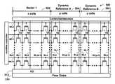
- FIG. 3is a schematic showing the interconnections of a portion 300 of a first sector 302 dynamic reference A 304 , and dynamic reference B 306 wherein dynamic reference A 304 and dynamic reference B 306 make up the reference array.
- Sector 1 302is shown having n cells. It should be appreciated that the sectors in a memory array can have other numbers of cells.
- Dynamic reference A 304 and dynamic reference B 306are shown having p cells each.
- Sector 302 , dynamic reference A 304 , and dynamic reference B 306have dual bit cells, such as cells 10 (only a few of which are shown) in an array with common wordlines, such as WL 0 , WL 1 and WLm connected to the dual bit cells 10 in a row and with common bitlines BL 0 -BLn in sector 1 302 , BL 0 -BLp in dynamic reference A 304 and BL 0 -BLp in dynamic reference B 306 .
- the wordlinesare common to both the dual bit cells in the sectors as well as the reference array.
- a Controller/Decoder 308controls the voltages to the individual bitlines and a wordline controller 310 controls the voltages to the individual wordlines.
- the bitlines in Sector 1terminate in an I/O 312 . Data from the I/O 312 and from the dynamic references A and B, 304 & 06 are controlled by a series of pass gates 314 .
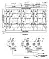
- FIG. 4is a schematic showing a comparison circuit 400 showing a core cell 402 , a cell 404 from dynamic reference A, and a cell 406 from dynamic reference B.
- the core cell 402has a CB (complimentary bit side) and an NB (normal bit side).
- the cells 404 and 406also have a CB side and an NB side.
- the data from the NB side of cell 402is being compared to averaged data from the dynamic reference cells 404 & 406 .
- the outputs of pass gates 410 , 414 & 416are input into cascode amplifiers 420 , 422 & 424 , respectively.
- the output of cascode amplifier 420is input into differential sense amplifier 426 and the output of cascode amplifiers 422 & 424 is input into the differential sense amplifier 426 , which then outputs o/p the correct value of the core cell.
- FIG. 5is a flow diagram 500 showing the steps to erase the memory cells in the sector array and associated reference array.
- the erase procedurestarts at 502 .
- the erase procedurepre-programs cells in the sector and associated reference array as indicated at 504 .
- the cellsare then subjected to an erase routine at 506 .
- a soft program steprepairs any cells that have been overerased during the erase step at 506 .
- appropriate cells in the reference arraysare programmed at 510 .
- the erase procedureis ended at 512 with the cells in the sector array erased and ready to be programmed and the cells in the reference array properly programmed and ready to be used as references. And now if the customer reads the newly erased sector, the customer will get the correct values of “1” that indicates erased bits.
- FIG. 6is a flow diagram 600 showing the programming of the reference cells.
- the reference cellsare arranged in two reference arrays. Cells in one reference array are programmed to 10. The cells in the other reference array are programmed to 01. One column is programmed as shown in FIG. 6, step 602 and the other column is programmed as shown in FIG. 6, step 604 .
- the described inventionprovides a dual bit flash memory array that allows dual bit operation of the flash memory device by allowing the use of dual dynamic references that are cycled with the dual bit memory cells in the flash memory and provides dual dynamic reference arrays that are immediately ready for use as references after a sector is erased.
Landscapes
- Engineering & Computer Science (AREA)
- Microelectronics & Electronic Packaging (AREA)
- Semiconductor Memories (AREA)
- Non-Volatile Memory (AREA)
- Read Only Memory (AREA)
- Techniques For Improving Reliability Of Storages (AREA)
Abstract
Description
| TABLE 1 | ||||||
| Operation | Gate | Bitline | 0 | Comment | ||
| read | C0 | 4.7 | v | 0 | v | 1.2-2 | v | complimentary |
| bit | ||||||||
| read | C1 | 4.7 | v | 1.2-2 | v | 0 | v | normal bit |
| program | C0 | Vpp | 5-6 | v | 0 | v | hot electron |
| program | C1 | Vpp | 0 | v | 5-6 | v | hot electron |
| one side- | C0 | −6 | v | 6 | v | 0 | V | hot hole injection |
| erase | ||||||||
| two side- | All | −6 | 6 | V | 6 | v | hot hole injection | |
| erase | cells | |||||||
Claims (17)
Priority Applications (9)
| Application Number | Priority Date | Filing Date | Title |
|---|---|---|---|
| US10/119,391US6690602B1 (en) | 2002-04-08 | 2002-04-08 | Algorithm dynamic reference programming |
| PCT/US2003/004611WO2003088260A1 (en) | 2002-04-08 | 2003-02-14 | Algorithm dynamic reference programming |
| AU2003219772AAU2003219772A1 (en) | 2002-04-08 | 2003-02-14 | Algorithm dynamic reference programming |
| KR1020047015998AKR100935948B1 (en) | 2002-04-08 | 2003-02-14 | Algorithm Dynamic Reference Programming |
| DE10392492.2TDE10392492B4 (en) | 2002-04-08 | 2003-02-14 | Algorithm-driven reference programming |
| JP2003585103AJP2005522817A (en) | 2002-04-08 | 2003-02-14 | Algorithm dynamic reference program |
| GB0420863AGB2401971B (en) | 2002-04-08 | 2003-02-14 | Algorithm dynamic reference programming |
| CNB038077426ACN100538897C (en) | 2002-04-08 | 2003-02-14 | The algorithm of dynamic reference programming |
| TW092107070ATWI286754B (en) | 2002-04-08 | 2003-03-28 | Algorithm dynamic reference programming |
Applications Claiming Priority (1)
| Application Number | Priority Date | Filing Date | Title |
|---|---|---|---|
| US10/119,391US6690602B1 (en) | 2002-04-08 | 2002-04-08 | Algorithm dynamic reference programming |
Publications (1)
| Publication Number | Publication Date |
|---|---|
| US6690602B1true US6690602B1 (en) | 2004-02-10 |
Family
ID=29248246
Family Applications (1)
| Application Number | Title | Priority Date | Filing Date |
|---|---|---|---|
| US10/119,391Expired - LifetimeUS6690602B1 (en) | 2002-04-08 | 2002-04-08 | Algorithm dynamic reference programming |
Country Status (9)
| Country | Link |
|---|---|
| US (1) | US6690602B1 (en) |
| JP (1) | JP2005522817A (en) |
| KR (1) | KR100935948B1 (en) |
| CN (1) | CN100538897C (en) |
| AU (1) | AU2003219772A1 (en) |
| DE (1) | DE10392492B4 (en) |
| GB (1) | GB2401971B (en) |
| TW (1) | TWI286754B (en) |
| WO (1) | WO2003088260A1 (en) |
Cited By (51)
| Publication number | Priority date | Publication date | Assignee | Title |
|---|---|---|---|---|
| US20040153620A1 (en)* | 2003-01-30 | 2004-08-05 | Shai Eisen | Address scramble |
| US20040222437A1 (en)* | 2000-12-07 | 2004-11-11 | Dror Avni | Programming and erasing methods for an NROM array |
| US20040257873A1 (en)* | 2003-06-20 | 2004-12-23 | Ming-Huei Shieh | Memory with a core-based virtual ground and dynamic reference sensing scheme |
| US20050058005A1 (en)* | 2002-01-31 | 2005-03-17 | Assaf Shappir | Method for operating a memory device |
| US20050117395A1 (en)* | 2002-01-31 | 2005-06-02 | Saifun Semiconductors Ltd. | Method for operating a memory device |
| US6917544B2 (en) | 2002-07-10 | 2005-07-12 | Saifun Semiconductors Ltd. | Multiple use memory chip |
| US20050276118A1 (en)* | 2004-06-10 | 2005-12-15 | Eduardo Maayan | Reduced power programming of non-volatile cells |
| US20060056240A1 (en)* | 2004-04-01 | 2006-03-16 | Saifun Semiconductors, Ltd. | Method, circuit and system for erasing one or more non-volatile memory cells |
| US20060068551A1 (en)* | 2004-09-27 | 2006-03-30 | Saifun Semiconductors, Ltd. | Method for embedding NROM |
| US20060109718A1 (en)* | 2004-11-24 | 2006-05-25 | Macronix International Co., Ltd. | System and method for preventing read margin degradation for a memory array |
| US7064983B2 (en) | 2001-04-05 | 2006-06-20 | Saifum Semiconductors Ltd. | Method for programming a reference cell |
| US20060146624A1 (en)* | 2004-12-02 | 2006-07-06 | Saifun Semiconductors, Ltd. | Current folding sense amplifier |
| US20060158940A1 (en)* | 2005-01-19 | 2006-07-20 | Saifun Semiconductors, Ltd. | Partial erase verify |
| US20060211188A1 (en)* | 2004-10-14 | 2006-09-21 | Saifun Semiconductors Ltd. | Non-volatile memory structure and method of fabrication |
| US7136304B2 (en) | 2002-10-29 | 2006-11-14 | Saifun Semiconductor Ltd | Method, system and circuit for programming a non-volatile memory array |
| US20060262598A1 (en)* | 1997-08-01 | 2006-11-23 | Saifun Semiconductors Ltd. | Two bit non-volatile electrically erasable and programmable semiconductor memory cell utilizing asymmetrical charge trapping |
| US20060274576A1 (en)* | 2005-06-03 | 2006-12-07 | Marco Redaelli | Sensing scheme for a non-volatile semiconductor memory cell |
| US20060274581A1 (en)* | 2005-06-03 | 2006-12-07 | Marco Redaelli | Reference scheme for a non-volatile semiconductor memory device |
| US20060285408A1 (en)* | 2005-06-17 | 2006-12-21 | Saifun Semiconductors, Ltd. | Method circuit and system for compensating for temperature induced margin loss in non-volatile memory cells |
| US20060285386A1 (en)* | 2005-06-15 | 2006-12-21 | Saifun Semiconductors, Ltd. | Accessing an NROM array |
| US20070025147A1 (en)* | 2005-07-28 | 2007-02-01 | Matsushita Electric Industrial Co., Ltd. | Non-volatile semiconductor memory device |
| US20070032016A1 (en)* | 2001-11-19 | 2007-02-08 | Saifun Semiconductors Ltd. | Protective layer in memory device and method therefor |
| US20070036007A1 (en)* | 2005-08-09 | 2007-02-15 | Saifun Semiconductors, Ltd. | Sticky bit buffer |
| US20070051982A1 (en)* | 2005-07-18 | 2007-03-08 | Saifun Semiconductors Ltd. | Dense non-volatile memory array and method of fabrication |
| US20070058439A1 (en)* | 2005-09-09 | 2007-03-15 | Macronix International Co., Ltd. | Systems and methods for a reference circuit in a dual bit flash memory device |
| US20070096199A1 (en)* | 2005-09-08 | 2007-05-03 | Eli Lusky | Method of manufacturing symmetric arrays |
| US7221138B2 (en) | 2005-09-27 | 2007-05-22 | Saifun Semiconductors Ltd | Method and apparatus for measuring charge pump output current |
| US20070120180A1 (en)* | 2005-11-25 | 2007-05-31 | Boaz Eitan | Transition areas for dense memory arrays |
| US20070133276A1 (en)* | 2003-09-16 | 2007-06-14 | Eli Lusky | Operating array cells with matched reference cells |
| US20070141788A1 (en)* | 2005-05-25 | 2007-06-21 | Ilan Bloom | Method for embedding non-volatile memory with logic circuitry |
| US20070153575A1 (en)* | 2006-01-03 | 2007-07-05 | Saifun Semiconductors, Ltd. | Method, system, and circuit for operating a non-volatile memory array |
| US20070159880A1 (en)* | 2006-01-12 | 2007-07-12 | Boaz Eitan | Secondary injection for NROM |
| US20070168637A1 (en)* | 2003-01-31 | 2007-07-19 | Yan Polansky | Memory array programming circuit and a method for using the circuit |
| US20070171717A1 (en)* | 2004-08-12 | 2007-07-26 | Saifun Semiconductors Ltd. | Dynamic matching of signal path and reference path for sensing |
| US20070173017A1 (en)* | 2006-01-20 | 2007-07-26 | Saifun Semiconductors, Ltd. | Advanced non-volatile memory array and method of fabrication thereof |
| US20070194835A1 (en)* | 2006-02-21 | 2007-08-23 | Alexander Kushnarenko | Circuit and method for powering up an integrated circuit and an integrated circuit utilizing same |
| US20070195607A1 (en)* | 2006-02-21 | 2007-08-23 | Saifun Semiconductors Ltd. | Nrom non-volatile memory and mode of operation |
| US20070253248A1 (en)* | 2006-04-27 | 2007-11-01 | Eduardo Maayan | Method for programming a reference cell |
| US20070255889A1 (en)* | 2006-03-22 | 2007-11-01 | Yoav Yogev | Non-volatile memory device and method of operating the device |
| US7317633B2 (en) | 2004-07-06 | 2008-01-08 | Saifun Semiconductors Ltd | Protection of NROM devices from charge damage |
| US20080037329A1 (en)* | 2005-03-28 | 2008-02-14 | Motoi Takahashi | Nonvolatile semiconductor memory, method for reading the same, and microprocessor |
| US20080094127A1 (en)* | 2006-09-18 | 2008-04-24 | Yoram Betser | Measuring and controlling current consumption and output current of charge pumps |
| US20080239599A1 (en)* | 2007-04-01 | 2008-10-02 | Yehuda Yizraeli | Clamping Voltage Events Such As ESD |
| US7532529B2 (en) | 2004-03-29 | 2009-05-12 | Saifun Semiconductors Ltd. | Apparatus and methods for multi-level sensing in a memory array |
| US7535765B2 (en) | 2004-12-09 | 2009-05-19 | Saifun Semiconductors Ltd. | Non-volatile memory device and method for reading cells |
| US20090168578A1 (en)* | 2007-12-31 | 2009-07-02 | Simtek | Dummy cell for memory circuits |
| US7638835B2 (en) | 2006-02-28 | 2009-12-29 | Saifun Semiconductors Ltd. | Double density NROM with nitride strips (DDNS) |
| US7668017B2 (en) | 2005-08-17 | 2010-02-23 | Saifun Semiconductors Ltd. | Method of erasing non-volatile memory cells |
| US7692961B2 (en) | 2006-02-21 | 2010-04-06 | Saifun Semiconductors Ltd. | Method, circuit and device for disturb-control of programming nonvolatile memory cells by hot-hole injection (HHI) and by channel hot-electron (CHE) injection |
| US20100329024A1 (en)* | 2009-06-29 | 2010-12-30 | Spansion Llc | Memory employing separate dynamic reference areas |
| US8053812B2 (en) | 2005-03-17 | 2011-11-08 | Spansion Israel Ltd | Contact in planar NROM technology |
Families Citing this family (7)
| Publication number | Priority date | Publication date | Assignee | Title |
|---|---|---|---|---|
| US6799256B2 (en)* | 2002-04-12 | 2004-09-28 | Advanced Micro Devices, Inc. | System and method for multi-bit flash reads using dual dynamic references |
| AU2003265452A1 (en) | 2002-09-20 | 2004-04-08 | Enventure Global Technology | Pipe formability evaluation for expandable tubulars |
| US7224619B2 (en)* | 2005-09-09 | 2007-05-29 | Macronix International Co., Ltd. | Method and apparatus for protection from over-erasing nonvolatile memory cells |
| JP4672024B2 (en)* | 2005-12-15 | 2011-04-20 | スパンション エルエルシー | Nonvolatile memory device and control method of nonvolatile memory device |
| KR100666223B1 (en)* | 2006-02-22 | 2007-01-09 | 삼성전자주식회사 | 3-level nonvolatile semiconductor memory device for reducing coupling noise between memory cells and driving method thereof |
| US7590001B2 (en) | 2007-12-18 | 2009-09-15 | Saifun Semiconductors Ltd. | Flash memory with optimized write sector spares |
| US8045390B2 (en)* | 2008-03-21 | 2011-10-25 | Macronix International Co., Ltd. | Memory system with dynamic reference cell and method of operating the same |
Citations (5)
| Publication number | Priority date | Publication date | Assignee | Title |
|---|---|---|---|---|
| US5163021A (en) | 1989-04-13 | 1992-11-10 | Sundisk Corporation | Multi-state EEprom read and write circuits and techniques |
| US5754475A (en) | 1996-06-24 | 1998-05-19 | Advanced Micro Devices, Inc. | Bit line discharge method for reading a multiple bits-per-cell flash EEPROM |
| US6108259A (en)* | 1998-06-12 | 2000-08-22 | Samsung Electronics, Co., Ltd. | Nonvolatile semiconductor memory device |
| EP1271550A2 (en) | 2001-06-20 | 2003-01-02 | Fujitsu Limited | Method and device for reading dual bit memory cells using multiple reference cells with two side read |
| US6538922B1 (en) | 2000-09-27 | 2003-03-25 | Sandisk Corporation | Writable tracking cells |
Family Cites Families (2)
| Publication number | Priority date | Publication date | Assignee | Title |
|---|---|---|---|---|
| JP3336813B2 (en) | 1995-02-01 | 2002-10-21 | ソニー株式会社 | Nonvolatile semiconductor memory device |
| JP4017118B2 (en)* | 2004-01-23 | 2007-12-05 | パイオニア株式会社 | Recording medium, recording apparatus and reproducing apparatus using ferroelectric substance |
- 2002
- 2002-04-08USUS10/119,391patent/US6690602B1/ennot_activeExpired - Lifetime
- 2003
- 2003-02-14KRKR1020047015998Apatent/KR100935948B1/ennot_activeExpired - Lifetime
- 2003-02-14JPJP2003585103Apatent/JP2005522817A/enactivePending
- 2003-02-14GBGB0420863Apatent/GB2401971B/ennot_activeExpired - Fee Related
- 2003-02-14AUAU2003219772Apatent/AU2003219772A1/ennot_activeAbandoned
- 2003-02-14CNCNB038077426Apatent/CN100538897C/ennot_activeExpired - Lifetime
- 2003-02-14WOPCT/US2003/004611patent/WO2003088260A1/enactiveApplication Filing
- 2003-02-14DEDE10392492.2Tpatent/DE10392492B4/ennot_activeExpired - Lifetime
- 2003-03-28TWTW092107070Apatent/TWI286754B/enactive
Patent Citations (5)
| Publication number | Priority date | Publication date | Assignee | Title |
|---|---|---|---|---|
| US5163021A (en) | 1989-04-13 | 1992-11-10 | Sundisk Corporation | Multi-state EEprom read and write circuits and techniques |
| US5754475A (en) | 1996-06-24 | 1998-05-19 | Advanced Micro Devices, Inc. | Bit line discharge method for reading a multiple bits-per-cell flash EEPROM |
| US6108259A (en)* | 1998-06-12 | 2000-08-22 | Samsung Electronics, Co., Ltd. | Nonvolatile semiconductor memory device |
| US6538922B1 (en) | 2000-09-27 | 2003-03-25 | Sandisk Corporation | Writable tracking cells |
| EP1271550A2 (en) | 2001-06-20 | 2003-01-02 | Fujitsu Limited | Method and device for reading dual bit memory cells using multiple reference cells with two side read |
Non-Patent Citations (1)
| Title |
|---|
| International Search Report dated Sep. 5, 2003, for International Application Ser. No. PCT/US03/04611. |
Cited By (99)
| Publication number | Priority date | Publication date | Assignee | Title |
|---|---|---|---|---|
| US20080111177A1 (en)* | 1997-08-01 | 2008-05-15 | Eduardo Maayan | Non-volatile memory cell and non-volatile memory device using said cell |
| US20060262598A1 (en)* | 1997-08-01 | 2006-11-23 | Saifun Semiconductors Ltd. | Two bit non-volatile electrically erasable and programmable semiconductor memory cell utilizing asymmetrical charge trapping |
| US7405969B2 (en) | 1997-08-01 | 2008-07-29 | Saifun Semiconductors Ltd. | Non-volatile memory cell and non-volatile memory devices |
| US20090032862A1 (en)* | 1997-08-01 | 2009-02-05 | Eduardo Maayan | Non-volatile memory cell and non-volatile memory device using said cell |
| US6937521B2 (en) | 2000-05-04 | 2005-08-30 | Saifun Semiconductors Ltd. | Programming and erasing methods for a non-volatile memory cell |
| US20040222437A1 (en)* | 2000-12-07 | 2004-11-11 | Dror Avni | Programming and erasing methods for an NROM array |
| US6928001B2 (en) | 2000-12-07 | 2005-08-09 | Saifun Semiconductors Ltd. | Programming and erasing methods for a non-volatile memory cell |
| US7064983B2 (en) | 2001-04-05 | 2006-06-20 | Saifum Semiconductors Ltd. | Method for programming a reference cell |
| US20070032016A1 (en)* | 2001-11-19 | 2007-02-08 | Saifun Semiconductors Ltd. | Protective layer in memory device and method therefor |
| US7190620B2 (en) | 2002-01-31 | 2007-03-13 | Saifun Semiconductors Ltd. | Method for operating a memory device |
| US20050117395A1 (en)* | 2002-01-31 | 2005-06-02 | Saifun Semiconductors Ltd. | Method for operating a memory device |
| US7420848B2 (en) | 2002-01-31 | 2008-09-02 | Saifun Semiconductors Ltd. | Method, system, and circuit for operating a non-volatile memory array |
| US20060126396A1 (en)* | 2002-01-31 | 2006-06-15 | Saifun Semiconductors, Ltd. | Method, system, and circuit for operating a non-volatile memory array |
| US20050058005A1 (en)* | 2002-01-31 | 2005-03-17 | Assaf Shappir | Method for operating a memory device |
| US7079420B2 (en) | 2002-01-31 | 2006-07-18 | Saifun Semiconductors Ltd. | Method for operating a memory device |
| US6917544B2 (en) | 2002-07-10 | 2005-07-12 | Saifun Semiconductors Ltd. | Multiple use memory chip |
| US7738304B2 (en) | 2002-07-10 | 2010-06-15 | Saifun Semiconductors Ltd. | Multiple use memory chip |
| US20060152975A1 (en)* | 2002-07-10 | 2006-07-13 | Eduardo Maayan | Multiple use memory chip |
| US7675782B2 (en) | 2002-10-29 | 2010-03-09 | Saifun Semiconductors Ltd. | Method, system and circuit for programming a non-volatile memory array |
| US7136304B2 (en) | 2002-10-29 | 2006-11-14 | Saifun Semiconductor Ltd | Method, system and circuit for programming a non-volatile memory array |
| US20040153620A1 (en)* | 2003-01-30 | 2004-08-05 | Shai Eisen | Address scramble |
| US6967896B2 (en) | 2003-01-30 | 2005-11-22 | Saifun Semiconductors Ltd | Address scramble |
| US20070168637A1 (en)* | 2003-01-31 | 2007-07-19 | Yan Polansky | Memory array programming circuit and a method for using the circuit |
| US7743230B2 (en) | 2003-01-31 | 2010-06-22 | Saifun Semiconductors Ltd. | Memory array programming circuit and a method for using the circuit |
| US20040257873A1 (en)* | 2003-06-20 | 2004-12-23 | Ming-Huei Shieh | Memory with a core-based virtual ground and dynamic reference sensing scheme |
| US20080117678A1 (en)* | 2003-06-20 | 2008-05-22 | Spansion Llc | Memory with a core-based virtual ground and dynamic reference sensing scheme |
| US7606068B2 (en) | 2003-06-20 | 2009-10-20 | Spansion Llc | Memory with a core-based virtual ground and dynamic reference sensing scheme |
| US7324374B2 (en)* | 2003-06-20 | 2008-01-29 | Spansion Llc | Memory with a core-based virtual ground and dynamic reference sensing scheme |
| US7457183B2 (en)* | 2003-09-16 | 2008-11-25 | Saifun Semiconductors Ltd. | Operating array cells with matched reference cells |
| US7864612B2 (en)* | 2003-09-16 | 2011-01-04 | Spansion Israel Ltd | Reading array cell with matched reference cell |
| US20070133276A1 (en)* | 2003-09-16 | 2007-06-14 | Eli Lusky | Operating array cells with matched reference cells |
| US20090231915A1 (en)* | 2003-09-16 | 2009-09-17 | Eli Lusky | Reading array cell with matched reference cell |
| US7532529B2 (en) | 2004-03-29 | 2009-05-12 | Saifun Semiconductors Ltd. | Apparatus and methods for multi-level sensing in a memory array |
| US20060056240A1 (en)* | 2004-04-01 | 2006-03-16 | Saifun Semiconductors, Ltd. | Method, circuit and system for erasing one or more non-volatile memory cells |
| US7652930B2 (en) | 2004-04-01 | 2010-01-26 | Saifun Semiconductors Ltd. | Method, circuit and system for erasing one or more non-volatile memory cells |
| US7366025B2 (en) | 2004-06-10 | 2008-04-29 | Saifun Semiconductors Ltd. | Reduced power programming of non-volatile cells |
| US20050276118A1 (en)* | 2004-06-10 | 2005-12-15 | Eduardo Maayan | Reduced power programming of non-volatile cells |
| US7317633B2 (en) | 2004-07-06 | 2008-01-08 | Saifun Semiconductors Ltd | Protection of NROM devices from charge damage |
| US7466594B2 (en) | 2004-08-12 | 2008-12-16 | Saifun Semiconductors Ltd. | Dynamic matching of signal path and reference path for sensing |
| US20070171717A1 (en)* | 2004-08-12 | 2007-07-26 | Saifun Semiconductors Ltd. | Dynamic matching of signal path and reference path for sensing |
| US20060068551A1 (en)* | 2004-09-27 | 2006-03-30 | Saifun Semiconductors, Ltd. | Method for embedding NROM |
| US7964459B2 (en) | 2004-10-14 | 2011-06-21 | Spansion Israel Ltd. | Non-volatile memory structure and method of fabrication |
| US7638850B2 (en) | 2004-10-14 | 2009-12-29 | Saifun Semiconductors Ltd. | Non-volatile memory structure and method of fabrication |
| US20060211188A1 (en)* | 2004-10-14 | 2006-09-21 | Saifun Semiconductors Ltd. | Non-volatile memory structure and method of fabrication |
| US20100173464A1 (en)* | 2004-10-14 | 2010-07-08 | Eli Lusky | Non-volatile memory structure and method of fabrication |
| CN100490013C (en)* | 2004-11-24 | 2009-05-20 | 旺宏电子股份有限公司 | System and method for preventing read margin reduction of memory array |
| US20060109718A1 (en)* | 2004-11-24 | 2006-05-25 | Macronix International Co., Ltd. | System and method for preventing read margin degradation for a memory array |
| US7262999B2 (en)* | 2004-11-24 | 2007-08-28 | Macronix International Co., Ltd. | System and method for preventing read margin degradation for a memory array |
| US20060146624A1 (en)* | 2004-12-02 | 2006-07-06 | Saifun Semiconductors, Ltd. | Current folding sense amplifier |
| US7535765B2 (en) | 2004-12-09 | 2009-05-19 | Saifun Semiconductors Ltd. | Non-volatile memory device and method for reading cells |
| US20060158940A1 (en)* | 2005-01-19 | 2006-07-20 | Saifun Semiconductors, Ltd. | Partial erase verify |
| US7468926B2 (en) | 2005-01-19 | 2008-12-23 | Saifun Semiconductors Ltd. | Partial erase verify |
| US7369440B2 (en) | 2005-01-19 | 2008-05-06 | Saifun Semiconductors Ltd. | Method, circuit and systems for erasing one or more non-volatile memory cells |
| US8053812B2 (en) | 2005-03-17 | 2011-11-08 | Spansion Israel Ltd | Contact in planar NROM technology |
| US7773425B2 (en)* | 2005-03-28 | 2010-08-10 | Fujitsu Semiconductor Limited | Nonvolatile semiconductor memory, method for reading the same, and microprocessor |
| US20080037329A1 (en)* | 2005-03-28 | 2008-02-14 | Motoi Takahashi | Nonvolatile semiconductor memory, method for reading the same, and microprocessor |
| CN101147201B (en)* | 2005-03-28 | 2010-07-28 | 富士通微电子株式会社 | Nonvolatile semiconductor memory, reading method thereof, and microprocessor |
| US20070141788A1 (en)* | 2005-05-25 | 2007-06-21 | Ilan Bloom | Method for embedding non-volatile memory with logic circuitry |
| US20060274581A1 (en)* | 2005-06-03 | 2006-12-07 | Marco Redaelli | Reference scheme for a non-volatile semiconductor memory device |
| US7259993B2 (en) | 2005-06-03 | 2007-08-21 | Infineon Technologies Ag | Reference scheme for a non-volatile semiconductor memory device |
| US20060274576A1 (en)* | 2005-06-03 | 2006-12-07 | Marco Redaelli | Sensing scheme for a non-volatile semiconductor memory cell |
| US7190621B2 (en) | 2005-06-03 | 2007-03-13 | Infineon Technologies Ag | Sensing scheme for a non-volatile semiconductor memory cell |
| US20060285386A1 (en)* | 2005-06-15 | 2006-12-21 | Saifun Semiconductors, Ltd. | Accessing an NROM array |
| US8400841B2 (en) | 2005-06-15 | 2013-03-19 | Spansion Israel Ltd. | Device to program adjacent storage cells of different NROM cells |
| US7184313B2 (en) | 2005-06-17 | 2007-02-27 | Saifun Semiconductors Ltd. | Method circuit and system for compensating for temperature induced margin loss in non-volatile memory cells |
| US20060285408A1 (en)* | 2005-06-17 | 2006-12-21 | Saifun Semiconductors, Ltd. | Method circuit and system for compensating for temperature induced margin loss in non-volatile memory cells |
| US20070051982A1 (en)* | 2005-07-18 | 2007-03-08 | Saifun Semiconductors Ltd. | Dense non-volatile memory array and method of fabrication |
| US7786512B2 (en) | 2005-07-18 | 2010-08-31 | Saifun Semiconductors Ltd. | Dense non-volatile memory array and method of fabrication |
| US20070025147A1 (en)* | 2005-07-28 | 2007-02-01 | Matsushita Electric Industrial Co., Ltd. | Non-volatile semiconductor memory device |
| US7417898B2 (en)* | 2005-07-28 | 2008-08-26 | Matsushita Electric Industrial Co., Ltd. | Non-volatile semiconductor memory device |
| US20070036007A1 (en)* | 2005-08-09 | 2007-02-15 | Saifun Semiconductors, Ltd. | Sticky bit buffer |
| US7668017B2 (en) | 2005-08-17 | 2010-02-23 | Saifun Semiconductors Ltd. | Method of erasing non-volatile memory cells |
| US20070096199A1 (en)* | 2005-09-08 | 2007-05-03 | Eli Lusky | Method of manufacturing symmetric arrays |
| US7289359B2 (en)* | 2005-09-09 | 2007-10-30 | Macronix International Co., Ltd. | Systems and methods for using a single reference cell in a dual bit flash memory |
| CN100524527C (en)* | 2005-09-09 | 2009-08-05 | 旺宏电子股份有限公司 | System and method for reference circuit in dual bit flash memory device |
| US20070058439A1 (en)* | 2005-09-09 | 2007-03-15 | Macronix International Co., Ltd. | Systems and methods for a reference circuit in a dual bit flash memory device |
| US7221138B2 (en) | 2005-09-27 | 2007-05-22 | Saifun Semiconductors Ltd | Method and apparatus for measuring charge pump output current |
| US20070120180A1 (en)* | 2005-11-25 | 2007-05-31 | Boaz Eitan | Transition areas for dense memory arrays |
| US20070153575A1 (en)* | 2006-01-03 | 2007-07-05 | Saifun Semiconductors, Ltd. | Method, system, and circuit for operating a non-volatile memory array |
| US7352627B2 (en) | 2006-01-03 | 2008-04-01 | Saifon Semiconductors Ltd. | Method, system, and circuit for operating a non-volatile memory array |
| US7808818B2 (en) | 2006-01-12 | 2010-10-05 | Saifun Semiconductors Ltd. | Secondary injection for NROM |
| US20070159880A1 (en)* | 2006-01-12 | 2007-07-12 | Boaz Eitan | Secondary injection for NROM |
| US20070173017A1 (en)* | 2006-01-20 | 2007-07-26 | Saifun Semiconductors, Ltd. | Advanced non-volatile memory array and method of fabrication thereof |
| US7760554B2 (en) | 2006-02-21 | 2010-07-20 | Saifun Semiconductors Ltd. | NROM non-volatile memory and mode of operation |
| US7692961B2 (en) | 2006-02-21 | 2010-04-06 | Saifun Semiconductors Ltd. | Method, circuit and device for disturb-control of programming nonvolatile memory cells by hot-hole injection (HHI) and by channel hot-electron (CHE) injection |
| US20070195607A1 (en)* | 2006-02-21 | 2007-08-23 | Saifun Semiconductors Ltd. | Nrom non-volatile memory and mode of operation |
| US8253452B2 (en) | 2006-02-21 | 2012-08-28 | Spansion Israel Ltd | Circuit and method for powering up an integrated circuit and an integrated circuit utilizing same |
| US20070194835A1 (en)* | 2006-02-21 | 2007-08-23 | Alexander Kushnarenko | Circuit and method for powering up an integrated circuit and an integrated circuit utilizing same |
| US7638835B2 (en) | 2006-02-28 | 2009-12-29 | Saifun Semiconductors Ltd. | Double density NROM with nitride strips (DDNS) |
| US20070255889A1 (en)* | 2006-03-22 | 2007-11-01 | Yoav Yogev | Non-volatile memory device and method of operating the device |
| US7701779B2 (en) | 2006-04-27 | 2010-04-20 | Sajfun Semiconductors Ltd. | Method for programming a reference cell |
| US20070253248A1 (en)* | 2006-04-27 | 2007-11-01 | Eduardo Maayan | Method for programming a reference cell |
| US20080094127A1 (en)* | 2006-09-18 | 2008-04-24 | Yoram Betser | Measuring and controlling current consumption and output current of charge pumps |
| US7605579B2 (en) | 2006-09-18 | 2009-10-20 | Saifun Semiconductors Ltd. | Measuring and controlling current consumption and output current of charge pumps |
| US20080239599A1 (en)* | 2007-04-01 | 2008-10-02 | Yehuda Yizraeli | Clamping Voltage Events Such As ESD |
| US7778098B2 (en)* | 2007-12-31 | 2010-08-17 | Cypress Semiconductor Corporation | Dummy cell for memory circuits |
| US20090168578A1 (en)* | 2007-12-31 | 2009-07-02 | Simtek | Dummy cell for memory circuits |
| US20100329024A1 (en)* | 2009-06-29 | 2010-12-30 | Spansion Llc | Memory employing separate dynamic reference areas |
| US7940570B2 (en)* | 2009-06-29 | 2011-05-10 | Spansion Llc | Memory employing separate dynamic reference areas |
Also Published As
| Publication number | Publication date |
|---|---|
| DE10392492B4 (en) | 2018-03-01 |
| TW200306577A (en) | 2003-11-16 |
| KR20040097313A (en) | 2004-11-17 |
| CN100538897C (en) | 2009-09-09 |
| GB2401971A (en) | 2004-11-24 |
| DE10392492T5 (en) | 2005-05-12 |
| GB0420863D0 (en) | 2004-10-20 |
| TWI286754B (en) | 2007-09-11 |
| CN1647213A (en) | 2005-07-27 |
| GB2401971B (en) | 2005-06-22 |
| JP2005522817A (en) | 2005-07-28 |
| WO2003088260A1 (en) | 2003-10-23 |
| AU2003219772A1 (en) | 2003-10-27 |
| KR100935948B1 (en) | 2010-01-12 |
Similar Documents
| Publication | Publication Date | Title |
|---|---|---|
| US6690602B1 (en) | Algorithm dynamic reference programming | |
| US6700815B2 (en) | Refresh scheme for dynamic page programming | |
| US6639844B1 (en) | Overerase correction method | |
| EP1518247B1 (en) | Method of erasing a flash memory using a pre-erasing step | |
| US6901010B1 (en) | Erase method for a dual bit memory cell | |
| EP1495471B1 (en) | System and method for generating a reference voltage based on averaging the voltages of two complementary programmed dual bit reference cells | |
| US7606068B2 (en) | Memory with a core-based virtual ground and dynamic reference sensing scheme | |
| US6834012B1 (en) | Memory device and methods of using negative gate stress to correct over-erased memory cells | |
| US6934190B1 (en) | Ramp source hot-hole programming for trap based non-volatile memory devices | |
| US7206241B2 (en) | Semiconductor device and programming method |
Legal Events
| Date | Code | Title | Description |
|---|---|---|---|
| AS | Assignment | Owner name:ADVANCED MICRO DEVICES, INC., CALIFORNIA Free format text:ASSIGNMENT OF ASSIGNORS INTEREST;ASSIGNORS:LE, BINH QUANG;CHEN, PAU-LING;REEL/FRAME:012798/0501 Effective date:20020404 | |
| STCF | Information on status: patent grant | Free format text:PATENTED CASE | |
| CC | Certificate of correction | ||
| AS | Assignment | Owner name:SPANSION INC., CALIFORNIA Free format text:ASSIGNMENT OF ASSIGNORS INTEREST;ASSIGNOR:ADVANCED MICRO DEVICES, INC.;REEL/FRAME:019047/0588 Effective date:20070131 | |
| AS | Assignment | Owner name:SPANSION LLC, CALIFORNIA Free format text:ASSIGNMENT OF ASSIGNORS INTEREST;ASSIGNOR:SPANSION INC.;REEL/FRAME:019069/0342 Effective date:20070131 | |
| FPAY | Fee payment | Year of fee payment:4 | |
| AS | Assignment | Owner name:BARCLAYS BANK PLC,NEW YORK Free format text:SECURITY AGREEMENT;ASSIGNORS:SPANSION LLC;SPANSION INC.;SPANSION TECHNOLOGY INC.;AND OTHERS;REEL/FRAME:024522/0338 Effective date:20100510 Owner name:BARCLAYS BANK PLC, NEW YORK Free format text:SECURITY AGREEMENT;ASSIGNORS:SPANSION LLC;SPANSION INC.;SPANSION TECHNOLOGY INC.;AND OTHERS;REEL/FRAME:024522/0338 Effective date:20100510 | |
| FPAY | Fee payment | Year of fee payment:8 | |
| AS | Assignment | Owner name:SPANSION TECHNOLOGY LLC, CALIFORNIA Free format text:RELEASE BY SECURED PARTY;ASSIGNOR:BARCLAYS BANK PLC;REEL/FRAME:035201/0159 Effective date:20150312 Owner name:SPANSION INC., CALIFORNIA Free format text:RELEASE BY SECURED PARTY;ASSIGNOR:BARCLAYS BANK PLC;REEL/FRAME:035201/0159 Effective date:20150312 Owner name:SPANSION LLC, CALIFORNIA Free format text:RELEASE BY SECURED PARTY;ASSIGNOR:BARCLAYS BANK PLC;REEL/FRAME:035201/0159 Effective date:20150312 | |
| AS | Assignment | Owner name:MORGAN STANLEY SENIOR FUNDING, INC., NEW YORK Free format text:SECURITY INTEREST;ASSIGNORS:CYPRESS SEMICONDUCTOR CORPORATION;SPANSION LLC;REEL/FRAME:035240/0429 Effective date:20150312 | |
| AS | Assignment | Owner name:CYPRESS SEMICONDUCTOR CORPORATION, CALIFORNIA Free format text:ASSIGNMENT OF ASSIGNORS INTEREST;ASSIGNOR:SPANSION, LLC;REEL/FRAME:036034/0415 Effective date:20150601 | |
| FPAY | Fee payment | Year of fee payment:12 | |
| AS | Assignment | Owner name:MUFG UNION BANK, N.A., CALIFORNIA Free format text:ASSIGNMENT AND ASSUMPTION OF SECURITY INTEREST IN INTELLECTUAL PROPERTY;ASSIGNOR:MORGAN STANLEY SENIOR FUNDING, INC.;REEL/FRAME:050896/0366 Effective date:20190731 | |
| AS | Assignment | Owner name:MORGAN STANLEY SENIOR FUNDING, INC., NEW YORK Free format text:CORRECTIVE ASSIGNMENT TO CORRECT THE 8647899 PREVIOUSLY RECORDED ON REEL 035240 FRAME 0429. ASSIGNOR(S) HEREBY CONFIRMS THE SECURITY INTERST;ASSIGNORS:CYPRESS SEMICONDUCTOR CORPORATION;SPANSION LLC;REEL/FRAME:058002/0470 Effective date:20150312 | |
| AS | Assignment | Owner name:SPANSION LLC, CALIFORNIA Free format text:RELEASE BY SECURED PARTY;ASSIGNOR:MUFG UNION BANK, N.A.;REEL/FRAME:059410/0438 Effective date:20200416 Owner name:CYPRESS SEMICONDUCTOR CORPORATION, CALIFORNIA Free format text:RELEASE BY SECURED PARTY;ASSIGNOR:MUFG UNION BANK, N.A.;REEL/FRAME:059410/0438 Effective date:20200416 | |
| AS | Assignment | Owner name:INFINEON TECHNOLOGIES LLC, CALIFORNIA Free format text:ASSIGNMENT OF ASSIGNORS INTEREST;ASSIGNOR:CYPRESS SEMICONDUCTOR CORPORATION;REEL/FRAME:059721/0467 Effective date:20200315 |