US6690467B1 - Optical system and method for optically analyzing light from a sample - Google Patents
Optical system and method for optically analyzing light from a sampleDownload PDFInfo
- Publication number
- US6690467B1 US6690467B1US09/564,790US56479000AUS6690467B1US 6690467 B1US6690467 B1US 6690467B1US 56479000 AUS56479000 AUS 56479000AUS 6690467 B1US6690467 B1US 6690467B1
- Authority
- US
- United States
- Prior art keywords
- light
- lens
- detection device
- optical element
- collection lens
- Prior art date
- Legal status (The legal status is an assumption and is not a legal conclusion. Google has not performed a legal analysis and makes no representation as to the accuracy of the status listed.)
- Expired - Fee Related
Links
Images


Classifications
- G—PHYSICS
- G01—MEASURING; TESTING
- G01J—MEASUREMENT OF INTENSITY, VELOCITY, SPECTRAL CONTENT, POLARISATION, PHASE OR PULSE CHARACTERISTICS OF INFRARED, VISIBLE OR ULTRAVIOLET LIGHT; COLORIMETRY; RADIATION PYROMETRY
- G01J3/00—Spectrometry; Spectrophotometry; Monochromators; Measuring colours
- G01J3/02—Details
- G01J3/0205—Optical elements not provided otherwise, e.g. optical manifolds, diffusers, windows
- G01J3/0208—Optical elements not provided otherwise, e.g. optical manifolds, diffusers, windows using focussing or collimating elements, e.g. lenses or mirrors; performing aberration correction
- G—PHYSICS
- G01—MEASURING; TESTING
- G01J—MEASUREMENT OF INTENSITY, VELOCITY, SPECTRAL CONTENT, POLARISATION, PHASE OR PULSE CHARACTERISTICS OF INFRARED, VISIBLE OR ULTRAVIOLET LIGHT; COLORIMETRY; RADIATION PYROMETRY
- G01J3/00—Spectrometry; Spectrophotometry; Monochromators; Measuring colours
- G01J3/02—Details
- G01J3/0205—Optical elements not provided otherwise, e.g. optical manifolds, diffusers, windows
- G01J3/0229—Optical elements not provided otherwise, e.g. optical manifolds, diffusers, windows using masks, aperture plates, spatial light modulators or spatial filters, e.g. reflective filters
- G—PHYSICS
- G01—MEASURING; TESTING
- G01J—MEASUREMENT OF INTENSITY, VELOCITY, SPECTRAL CONTENT, POLARISATION, PHASE OR PULSE CHARACTERISTICS OF INFRARED, VISIBLE OR ULTRAVIOLET LIGHT; COLORIMETRY; RADIATION PYROMETRY
- G01J3/00—Spectrometry; Spectrophotometry; Monochromators; Measuring colours
- G01J3/02—Details
- G01J3/0262—Constructional arrangements for removing stray light
- G—PHYSICS
- G01—MEASURING; TESTING
- G01J—MEASUREMENT OF INTENSITY, VELOCITY, SPECTRAL CONTENT, POLARISATION, PHASE OR PULSE CHARACTERISTICS OF INFRARED, VISIBLE OR ULTRAVIOLET LIGHT; COLORIMETRY; RADIATION PYROMETRY
- G01J3/00—Spectrometry; Spectrophotometry; Monochromators; Measuring colours
- G01J3/02—Details
- G01J3/0294—Multi-channel spectroscopy
- G—PHYSICS
- G01—MEASURING; TESTING
- G01J—MEASUREMENT OF INTENSITY, VELOCITY, SPECTRAL CONTENT, POLARISATION, PHASE OR PULSE CHARACTERISTICS OF INFRARED, VISIBLE OR ULTRAVIOLET LIGHT; COLORIMETRY; RADIATION PYROMETRY
- G01J3/00—Spectrometry; Spectrophotometry; Monochromators; Measuring colours
- G01J3/02—Details
- G01J3/04—Slit arrangements slit adjustment
- G—PHYSICS
- G01—MEASURING; TESTING
- G01J—MEASUREMENT OF INTENSITY, VELOCITY, SPECTRAL CONTENT, POLARISATION, PHASE OR PULSE CHARACTERISTICS OF INFRARED, VISIBLE OR ULTRAVIOLET LIGHT; COLORIMETRY; RADIATION PYROMETRY
- G01J3/00—Spectrometry; Spectrophotometry; Monochromators; Measuring colours
- G01J3/28—Investigating the spectrum
- G01J3/2803—Investigating the spectrum using photoelectric array detector
- G—PHYSICS
- G01—MEASURING; TESTING
- G01N—INVESTIGATING OR ANALYSING MATERIALS BY DETERMINING THEIR CHEMICAL OR PHYSICAL PROPERTIES
- G01N21/00—Investigating or analysing materials by the use of optical means, i.e. using sub-millimetre waves, infrared, visible or ultraviolet light
- G01N21/01—Arrangements or apparatus for facilitating the optical investigation
- G01N21/03—Cuvette constructions
- G01N21/05—Flow-through cuvettes
- G—PHYSICS
- G01—MEASURING; TESTING
- G01N—INVESTIGATING OR ANALYSING MATERIALS BY DETERMINING THEIR CHEMICAL OR PHYSICAL PROPERTIES
- G01N21/00—Investigating or analysing materials by the use of optical means, i.e. using sub-millimetre waves, infrared, visible or ultraviolet light
- G01N21/17—Systems in which incident light is modified in accordance with the properties of the material investigated
- G01N21/25—Colour; Spectral properties, i.e. comparison of effect of material on the light at two or more different wavelengths or wavelength bands
- G01N21/31—Investigating relative effect of material at wavelengths characteristic of specific elements or molecules, e.g. atomic absorption spectrometry
- G—PHYSICS
- G01—MEASURING; TESTING
- G01N—INVESTIGATING OR ANALYSING MATERIALS BY DETERMINING THEIR CHEMICAL OR PHYSICAL PROPERTIES
- G01N27/00—Investigating or analysing materials by the use of electric, electrochemical, or magnetic means
- G01N27/26—Investigating or analysing materials by the use of electric, electrochemical, or magnetic means by investigating electrochemical variables; by using electrolysis or electrophoresis
- G01N27/416—Systems
- G01N27/447—Systems using electrophoresis
- G01N27/44704—Details; Accessories
- G01N27/44717—Arrangements for investigating the separated zones, e.g. localising zones
- G01N27/44721—Arrangements for investigating the separated zones, e.g. localising zones by optical means
- G—PHYSICS
- G01—MEASURING; TESTING
- G01N—INVESTIGATING OR ANALYSING MATERIALS BY DETERMINING THEIR CHEMICAL OR PHYSICAL PROPERTIES
- G01N21/00—Investigating or analysing materials by the use of optical means, i.e. using sub-millimetre waves, infrared, visible or ultraviolet light
- G01N21/01—Arrangements or apparatus for facilitating the optical investigation
- G01N21/03—Cuvette constructions
- G01N2021/0346—Capillary cells; Microcells
Definitions
- This inventionrelates to an optical system for analyzing light from a sample holder.
- the optical systemis particularly suitable for use in a single or multi-channel separation system.
- the present inventionis also directed toward a method of optically analyzing light from a separation system using a spectrograph.
- Spectrographsare devices for separating electromagnetic radiation into its spectral components. Optical spectrographs can be used for analysis of samples, such as analyzing the chemical composition of nucleic acid samples in order to determine the nucleotide sequence of the sample.
- samplessuch as analyzing the chemical composition of nucleic acid samples in order to determine the nucleotide sequence of the sample.
- experiments in chemistry and biologytypically involve evaluating large numbers of samples. Sequencing of nucleic acid samples is typically time consuming and labor intensive. Therefore, it is desirable that a large number of samples can be simultaneously analyzed. With large scale projects such as the Human Genome Project, it is desirable to increase throughput of nucleic acid sequencing.
- Electrophoresisis an increasingly common method of performing analysis, e.g. sequencing, of biological substances in order to increase throughput. Electrophoresis is an electrochemical process in which molecules with a net charge migrate in a solution under the influence of an electric current. Electrophoresis using one or more capillaries which are illuminated by a laser has proven to be useful in analyzing biological substances. Existing systems are typically not well-adapted for imaging large numbers of samples with a small focal ratio and high light collecting ability. Therefore, there is a need for an apparatus and method that maintains a substantially uniform image quality over a large field of view. Preferably, such an apparatus is compact, simple, and reduces focusing problems.
- the inventionincludes an optical system for analyzing light from a plurality of samples.
- the optical systemincludes a plurality of sample holders, a collection lens, a reimaging lens, and a light dispersing element located between the collection lens and the reimaging lens.
- the collection lensis configured to receive and substantially collimate light from the samples.
- the light dispersing elementis configured to spectrally disperse the substantially collimated light from the collection lens.
- the reimaging lensis configured to receive light from the light dispersing element and direct the light onto a light detection device.
- the inventionis directed towards a system for analyzing light from a sample in a separation system.
- the systemincludes at least one separation lane, a collection lens, a reimaging lens, and a light dispersing element located between the collection lens and the reimaging lens.
- the light sourceprovides an excitation light to the at least one separation lane.
- the collection lensis configured to receive and substantially collimate light emitted from the separation lane.
- the light dispersing elementis configured to spectrally disperse substantially collimated light from the collection lens.
- the reimaging lensis configured to receive dispersed light from the light dispersing element and direct the light onto a light detection device.
- the systemmay include a light source providing an excitation light to the at least one separation lane.
- the systemmay include a plurality of the separation lanes.
- the inventionincludes an optical spectrograph for analyzing light from at least one sample.
- the optical spectrographincludes at least one source of excitation light for illuminating at least one sample holder, a first lens unit, a transmission grating, a second lens unit, and a light detection device having a plurality of detector elements.
- the first lens unithas at least one lens and is configured to receive and substantially collimate light from the sample holder.
- the excitation light from the source of illuminationdoes not pass through the first lens unit prior to illuminating the at least one sample holder.
- the transmission gratingis configured to spectrally disperse substantially collimated light from the first lens unit.
- the second lens unithas at least one lens and is configured to receive light from the transmission grating and direct the light onto the light detection device.
- the inventionis directed toward a method of optically analyzing at least one sample.
- the methodincludes providing at least one holder having a sample therein, illuminating the sample with an excitation light to generate an emission light, and collecting the emission light from the sample with a collection lens.
- the excitation lightdoes not pass through the collection lens prior to illuminating the sample.
- the emission lightis substantially collimated by the collection lens.
- the methodfurther includes spectrally dispersing the substantially collimated emission light beam with a transmission grating, directing the emission light from the transmission grating onto a light detection device by a reimaging lens, and optically detecting the spectral characteristics of the emission light.
- a plurality of sample holdersare provided.
- FIG. 1is a side view of an optical system for analyzing light according to certain embodiments of the present invention
- FIG. 2is a perspective view of an array of capillaries of a separation system which may be used with the present invention
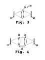
- FIG. 3is a schematic of an optical system having a single lens
- FIG. 4is a schematic of an optical system according to the present invention having two lenses
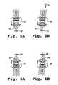
- FIGS. 5A and 5Bare schematics illustrating the effect of a light source being positioned at the optical axis and offset perpendicular from the optical axis, respectively, as the light passes through a collection lens;
- FIGS. 6A and 6Bare schematics illustrating the light rays of FIGS. 5A and 5B, respectively, passing through a reimaging lens onto a light detection device;
- FIGS. 7A and 7Bare schematics illustrating the effect of a light having different wavelength components, such as blue and red light, respectively, as the light passes through the collection lens;
- FIGS. 8A and 8Bare schematics illustrating the blue and red components of FIGS. 7A and 7B, respectively, passing through the reimaging lens onto a light detection device;
- FIG. 9illustrates incident light being spectrally dispersed by a transmission grating
- FIG. 10illustrates the channels on an optical detection device such as a CCD, according to certain embodiments of the present invention
- FIGS. 11A-11Cillustrate the position of an image relative to the desired image plane for light having a long wavelength, medium wavelength, and short wavelength, respectively;
- FIG. 12is a schematic illustrating the effect of chromatic aberration on focusing in certain embodiments of the present invention.
- FIG. 13is a schematic illustrating the effect of tilting a detection plane of a CCD to reduce chromatic aberration
- FIG. 14is a side view of a system for testing the amount of tilting of the detection plane of the CCD to bring the image into focus;
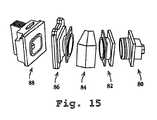
- FIG. 15is a perspective view of an optical system according to an embodiment of the present invention.
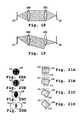
- FIG. 16is a side view of an optical system, illustrating the curved field of focus in certain systems that do not include a correction lens;
- FIG. 17is a side view of an optical system according to embodiments of the present invention, with a correction lens.
- FIG. 18is a schematic of an optical system with no vignetting
- FIG. 19is a schematic of an optical system with vignetting
- FIGS. 20A-20Dare front views illustrating the effect of vignetting as the angle of the incident light becomes more offset
- FIGS. 21A-21Dare top views corresponding to FIGS. 20A-20D respectively;
- FIG. 22is a side view of an optical system according to certain embodiments of the present invention with a light source on the optical axis so that no vignetting occurs;
- FIG. 23is a side view of the optical system of FIG. 22 with the light source displaced from the optical axis so that vignetting occurs;
- FIG. 24illustrates a cat's eye aperture according to certain embodiments of the present invention.
- FIGS. 25A-25Eare front views illustrating the effect of the cat's eye aperture of FIG. 24 on the light throughput of an optical system
- FIGS. 26A-26Eare top views corresponding to FIGS. 25A-25E respectively.
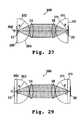
- FIG. 27is a schematic of an optical system according to an embodiment of the present invention, with a hemispherical element
- FIG. 28is a side view of an embodiment of the optical system of FIG. 27.
- FIG. 29is a schematic of another optical system with a hemispherical element.
- the present inventionprovides an optical system for analyzing light from a plurality of samples.
- the optical systemgenerally includes a plurality of sample holders, a collection lens configured to receive and substantially collimate light from the sample holders, a light dispersing element such as a transmission grating configured to spectrally disperse the substantially collimated light from the collection lens, and a reimaging lens configured to receive the light from the light dispersing element and direct the light onto a light detection device.
- the sample holdersare located substantially at the image plane of the collection lens.
- the optical systemis used in a separation system having a plurality of separation lanes.
- the present inventionfurther provides methods of optically analyzing at least one sample in a spectrograph.
- the methodincludes providing at least one sample holder having a sample therein, illuminating the sample with an excitation light to generate an emission light, and collecting the emission light from the sample with a collection lens.
- the excitation lightdoes not pass through the collection lens prior to illuminating the sample.
- the emission lightis substantially collimated by the collection lens.
- the methodfurther includes spectrally dispersing the substantially collimated emission light with a light dispersing element, such as a transmission grating, directing the emission light from the light dispersing element onto a light detection device by a reimaging lens, and optically detecting the spectral characteristics of the emission light.
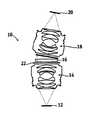
- FIG. 1shows an example of an optical system for analyzing light from a sample according to certain embodiments of the present invention.
- optical system 10includes at least one sample holder, with a sample contained therein.
- the sampleis preferably located at or near the object plane 12 .
- the object planeis a plane at the focal distance from the collection lens 14 .
- the optical systemfurther includes a collection lens 14 , a light dispersing element 16 , a reimaging lens 18 , and an optical detection device 20 .
- the optical systemfurther includes an excitation light blocking filter 22 positioned between the collection lens 14 and the light dispersing element 16 .
- the optical systemincludes at least one sample holder for containing a sample.
- the present inventionwill be described herein for use with a plurality of sample holders. However, the present invention is also suitable for use with a single sample holder.
- the sample holderscomprise a plurality of separation lanes, such as electrophoresis capillaries, located within the object plane of the collection lens.
- a separation laneis a path along which migrating sample components are separated, for example, using electrophoresis, chromatography, sedimentation, or other separation processes.
- FIG. 2shows an example of a capillary arrangement suitable for use with the optical system of certain embodiments of the present invention. This capillary arrangement is known in the art, and is used for purposes of example only.
- FIG. 2The capillary arrangement shown in FIG. 2 is described in greater detail in U.S. Pat. No. 5,498,324 to Yeung et al., the disclosure of which is hereby incorporated in its entirety herein for any purpose.
- Other similar capillary arrangementsare described in U.S. Pat. No. 5,938,908 to Anazawa et al., the disclosure of which is also hereby incorporated in its entirety herein for any purpose.
- the capillary system 200is particularly suited for capillary electrophoresis.
- the capillary system 200includes an array of capillaries 202 with optical fibers 204 inserted into an outflow end of the capillaries 202 .
- a laseris directed at the ends of the optical fibers.
- Spacing capillaries 206 with black coatingare placed between each of the capillaries 202 used for separation. Spacing capillaries 206 act as spacers to prevent crosstalk between separation capillaries 202 .
- This capillary systemis described in greater detail in U.S. Pat. No. 5,498,324 to Yeung et al.
- sixteen capillariesare provided. This number may be varied to range from one to several hundred, depending on the field of view and size and quality of the optical system.
- sample holderscould be used including oligonucleotide arrays as described for example in U.S. Pat. No. 5,445,934 to Fodor et al., and microfluidic devices as described for example in WO97/36681 to Woudenberg et al., the disclosures of which are both hereby incorporated by reference in their entirety herein for any purpose.
- Other types of sample holders suitable for use with the present inventioninclude, but are not limited to, wells, slides, test tubes or any other sample holding device able to confine a sample to a known location.
- an optical system 10 of the present inventionmay be positioned perpendicular to the capillary array.
- an excitation sourcesuch as a laser for generating an excitation light to illuminate the sample (or samples) in the sample holder (or sample holders).
- excitation sourcesmay be provided.
- excitationis provided to the sample by an Argon ion laser as discussed generally above, and in greater detail in U.S. Pat. No. 5,498,324 to Yeung et al.
- Other types of conventional excitation sourcesmay also be used, such as an arc lamp (e.g., mercury/xenon lamp, mercury vapor lamp), xenon lamp, tungsten/halogen lamp, deuterium lamp, light emitting diode (LED), or high-intensity discharge (HID) lamp.
- the excitation sourceis typically selected to emit excitation light at one or several wavelengths or wavelength ranges absorbed by the sample or samples. In one specific example, lasers having a wavelength of 488 and 514 nm are used.
- the sampleWhen the sample is illuminated by a laser or other excitation source, the sample acts as a light source and emits an emission light.
- a laser or excitation sourceIn certain particular embodiments, two lasers are used.
- the provision of a laser or excitation source on opposite sides of the capillaries in certain embodimentshelps to provide a more uniform intensity across a row of samples.
- Some applications of the present inventiondo not require an excitation source in order to illuminate the sample. For example, in chemilluminescence and electrochemilluminescence, a sample emits light without an excitation light source.
- the sampleis located at approximately the focal distance (at the object plane) from the collection lens 14 so that the light emitted from the sample (the emission light) upon being struck with an excitation light (e.g., laser beam) will be optimally collected by the collection lens 14 .
- the sampleis preferably positioned at or near the object plane of the collection lens.
- the collection lens 14is configured to receive and substantially collimate light from at least one sample holder.
- the collection lensis a type of lens that is spaced from the sample and that can collect light.
- An emission light from the sampleis collected by the collection lens and directed toward a light dispersing element.
- the collection lens 14may include a single lens or an assembly of multiple lenses, but will be referred to as a single lens for purposes of illustration. Because the collection lens is a collimating lens, light from the sample holder(s) will be converted into substantially parallel (or collimated) light rays as it passes through the collection lens.
- a source of lighte.g., capillary tube
- the emission light from the samplewill be collimated along the optical axis 15 of the collection lens 14 , as shown in FIG. 5 A.
- the emission lightwill be collimated but at an angle ⁇ to the optical axis 15 of the collection lens 14 .
- Each point on the collection lens' object plane 12maps to a unique angle ⁇ as light emitted from the point passes through the collection lens. Therefore, in the system of the present invention, a plurality of spaced-apart sample holders (e.g., capillary tubes) may be imaged by the same collection lens.
- a collimating lenssuch as the collection lens 14 functions to convert spatial information into angular information.
- a collimating lenssuch as collection lens 14 provides a substantially collimated region 26 as shown in FIG. 4 .
- the lightis substantially collimated in the region between the collection lens 14 and reimaging lens 18 .
- the collimated regionis particularly well suited for the insertion of a variety of optical devices (e.g., apertures, interference filters, etc.).
- An optical lens system with a plurality of lensese.g., a relay lens system
- one lens 30both collects light from an object plane 12 and refocuses the light to an image plane 20 .
- the single lens systemcannot provide a collimated region for the insertion of optical devices, a disadvantage compared to the present invention.
- a lens that may be used as a collection lens in the present inventioninclude, but are not limited to, any positive lens, i.e., a lens that brings collimated light to a focus.
- positive lensesmay include, for example, a still camera lens, a CCD video camera lens, a microscope objective, or an achromatic lens.
- a light dispersing elementmay be provided, along with other optical devices, in the substantially collimated region 26 between the collection lens 14 and reimaging lens 18 .
- the collection lenssubstantially collimates the light and directs it to the light dispersing element.
- a light dispersing elementcan be any element that spectrally separates incoming light into its spectral components. For example, incoming light can be deflected at an angle roughly proportional to the wavelength of the light. Thus, different wavelengths are separated.
- the light dispersing element discussedwill be a transmission grating.
- a transmission gratingthe light rays that strike the grating surface are transmitted through the grating.
- rays of light that strike a transmission grating surfacedeflect at an angle roughly proportional to the wavelength of the light.
- the transmission gratingcan be of several types, such as a flat blazed grating. Blazed gratings have a triangular, saw-tooth shape. The shape of each groove functions like a prism to refract the light.
- a gratingwill have hundreds or thousands of grooves per mm.
- the grating groove densitymay range from about 100 grooves/mm to about 1,200 grooves/mm. This range is for purposes of example only, as larger and smaller groove densities may also be used with the present invention.
- FIG. 9illustrates an incident light 40 striking a transmission grating and being dispersed spectrally into a plurality of distinct light rays 42 , 44 , 46 , 48 , each corresponding to a particular wavelength component of incident light 40 .
- FIGS. 7A and 7Bshow light being emitted from a point on the object plane at the optical axis 15 of the collection lens 14 .
- the emission lightis collimated by the collection lens 14 and strikes the transmission grating 16 .
- the transmission gratingstrikes the transmission grating.
- the lightis dispersed spectrally. With spectral dispersion, a first light ray of a first wavelength will be deflected at a different angle with respect to the optical axis than a second light ray of a second wavelength. This effect is illustrated in FIGS.
- the light dispersing elementspreads the light spectrally in a direction substantially perpendicular to the spectral channels on the light detection device.
- This configurationcreates a two-dimensional image on the light detection device after the light passes through the reimaging lens 18 ; in the first direction the light is spectrally dispersed, in a second direction the light is spatially resolved/separated.
- the lightforms a plurality of images corresponding to channels on the light detection device so that the light from each channel may be analyzed for its spectral components.
- a variety of other types of light dispersing elementssuch as reflection gratings or prisms may be used with the present invention, although a transmission grating is preferred.
- the basic principles of the present inventionare applicable with a variety of other types of light dispersing elements such as prisms, grating prisms (“grisms”), and one or more dichroic filters.
- the light dispersing elementdisperses the collimated light and directs the light toward a reimaging lens.
- the reimaging lens 18receives the spectrally dispersed, but still collimated, light from the light dispersing element and directs it to the light detection device.
- the reimaging lens 18also known as a focusing lens in certain embodiments, takes a collimated light and directs it at or near a point on the image plane of the reimaging lens.
- the reimaging lens 18is optically identical to the collection lens 14 , except that the lens are reversed in direction so that they face each other.
- the image formed by the reimaging lens on the light detection devicemay be at a 1:1 ratio with the sample being analyzed, or it may be magnified or demagnified.
- the reimaging lens 18receives the substantially collimated light from the collection lens, and directs the light toward an image plane 20 .
- the incident collimated lightis centered along the optical axis 19 of the reimaging lens 18 , the light will be focused on the image plane 20 at the optical axis 19 of the reimaging lens, as shown in FIG. 6 A.
- the incident collimated lightis angled relative to the optical axis 19 of the reimaging lens 18 (such as shown in FIG. 5 B), the light will be focused on or near the image plane offset from the optical axis 19 of the reimaging lens, as shown in FIG. 6 B.
- the angle of the collimated light relative to the optical axis 19 of the reimaging lensdetermines a unique location on the image plane 20 of the reimaging lens (within the field of view).
- the angular displacement of the light from the collection lensis converted into a spatial displacement on the light detection device (e.g., CCD) by the reimaging lens.
- the optical systemcan focus light from a plurality of light sources (e.g., a plurality of illuminated capillary tubes).
- light from a given sampletypically includes components having different wavelengths. As shown for example in FIGS. 8A and 8B, these different components (blue and red in the example shown) will remain collimated after passing through the light dispersing element. As shown in FIG. 8A, when the blue collimated rays pass through the reimaging lens, the blue rays will be focused onto a first location on the image plane 20 . As shown in FIG. 8B, the red collimated rays also pass through the reimaging lens and are focused on a second location on the image plane 20 . The second location is displaced from the first location.
- the spectrum for each capillary tube (or other type of sample holder) that is formed on the light detecting deviceis referred to as a channel.
- the number of channelscorresponds to the number of capillary tubes in the field of view.
- the image plane of the reimaging lensis located coplanar with the light detection device 20 for optimized detection.
- a light detection deviceanalyzes light from a sample for its spectral components.
- the light detection devicecomprises a multi-element photodetector.
- the termmeans a detector having a plurality of addressable detector elements.
- Exemplary multi-element photodetectorsmay include, for example, charge-coupled devices (CCDs), diode arrays, photo-multiplier tube arrays and charge-injection devices (CIDs).
- CCDscharge-coupled devices
- diode arraysdiode arrays
- photo-multiplier tube arraysand charge-injection devices (CIDs).
- CIDscharge-injection devices
- the light dispersing elementspecifically a transmission grating in certain embodiments, spectrally spreads the light from each capillary tube so that it can be spectrally analyzed by a CCD.
- a transmission gratingin certain embodiments, spectrally spreads the light from each capillary tube so that it can be spectrally analyzed by a CCD.
- a single photosensorif only one sample or capillary tube is used, it may be desirable to use a single photosensor.
- An optical detection devicesuch as a CCD has an array of detection units, or pixels, arranged on a planar surface.
- a CCDwill typically have a large number of pixels, usually several hundred in each of the two axis. Each pixel will map to a specific channel or portion thereof and specific color (wavelength) of light from a sample in a specific capillary.
- the CCDhas two axes: a spatial axis and a spectral axis. This is shown in FIG. 10 which illustrates an example with five channels 50 on the CCD. Each channel spaced along the spatial axis (x-axis) corresponds to an individual capillary tube. For example, if sixteen capillary tubes are used, there will be sixteen channels on the CCD. In certain embodiments, it is preferred to analyze the center of the sample to get the most accurate results, therefore only the pixels at or adjacent the center of each channel will be analyzed. In certain embodiments of the present invention, the capillary tubes have an inner diameter of approximately 50 ⁇ m, which corresponds to about two or three pixels.
- the spectral axis (y-axis)contains spectral information (e.g., wavelength vs. intensity information) for each of the capillary tubes. The axes could also be reversed if desired.
- the optical systemmay further include one or more blocking filters to prevent significant amounts of excitation light or other background light (e.g., Raman light, ambient light, etc.) from reaching the light detecting device.
- one or more excitation blocking filterssuch as long-pass filters, may be provided in the emission optical path. Excitation blocking filters prevent certain types of excitation light from entering the emission optical path of the optical system.
- FIG. 1shows an excitation blocking filter 22 positioned between the collection lens 14 and the transmission grating.
- interference filtersmay be used as excitation blocking filters in the optical system.
- interference filterssuch as notch, long-pass, and band-pass filters.
- colored glass filterssuch as long-pass and band-pass filters
- Interference filtersmay be configured to significantly block wavelengths below a predetermined threshold from passing to the reimaging lens.
- Excitation blocking filtersmay also be placed at a variety of other positions, such as prior to the collection lens (e.g., between the sample and the collection lens).
- the collimated regionis particularly suited for interference filters, because interference filters typically operate most efficiently when the incident light striking the filter is perpendicular to the surface of the filter (and the light is collimated).
- An interference filter in the collimated regionwill preferably be positioned between the collection lens and the transmission grating.
- Onemay use more than one excitation blocking filter at different positions, or may use one excitation blocking filter at any of the possible positions.
- the present inventionmay also be particularly configured to reduce chromatic aberration.
- Chromatic aberrationis a variation in focal length (and focus quality) with wavelength. Chromatic aberration may be particularly troublesome with wavelengths in the non-visible range, such as infra-red or near infra-red wavelengths.
- FIGS. 11A-11Cillustrate the effect of wavelength on the extent of chromatic aberration as represented by the position of the focal point 23 relative to the mid-wavelength image plane 20 of reimaging lens 18 .
- FIG. 11Ademonstrates that for a longer wavelength, the position of focal point 23 is beyond the mid-wavelength image plane 20 .
- FIG. 11Bdemonstrates that for a middle, optimum wavelength, the position of focal point 23 occurs at the mid-wavelength image plane 20 .
- FIG. 11Cdemonstrates that for a short wavelength, the position of focal point occurs before the mid-wavelength image plane 20 .
- FIG. 12illustrates a possible effect of chromatic aberration on the performance of the optical system.
- the light rays in the center of the image planeat the optical axis of the reimaging lens
- those at the edgeswill be out of focus.
- It is desirable to minimize chromatic aberrationi.e., have the light rays focused on the light detection device at both the center and the edges of the image plane) in order to increase the quality of the image obtained.
- tilting the plane of the light detection device 21can assist in reducing chromatic aberration as described in FIG. 12 .
- tilting the planar surface 21 of the light detecting device (CCD) by a slight angle with respect to the optical axis of the collection lenscompensates for chromatic aberration, thereby improving the quality of the image on the CCD over a wider spectrum of the light wavelength.
- Other adjustments besides tilting the planar surface of the light detection devicemay also be used in order to minimize the effect of chromatic aberration on the quality of the image.
- one or both of the collection lens and transmission gratingmay be tilted with respect to the optical axis of the collection lens.
- any of the filtersmay be also be tilted with respect to the optical axis of the collection lens.
- the tilting of the light detection devicealso assists in reducing the amount of stray light that is reflected off of the light detection device back into the system. Stray light may reduce the desired signal to noise values or cause channel to channel cross-contamination.
- Another method of reducing stray light, besides tilting the light detection device,is to provide anti-reflective coating on the light detection device.
- the anti-reflective coatingmay be provided on the window of the light detection device, or on the planar surface of the light detection device itself. It may also be desirable to provide an anti-reflective coating on any and all of the elements that the light passes through.
- a device and technique for determining the optimal angle of tilt of a planar light detection deviceis provided.
- the detection devicee.g., CCD
- the detection devicemay be tilted at various angles and the resulting images examined for focus quality along a spectral axis of the light detection device.
- the focus along the edges of the imageis then compared to the focus in the center of the image.
- the systemincludes a collection lens 60 , transmission grating 62 , reimaging lens 64 , and charge-coupled device (CCD) 66 , which may be identical to the collection lens 14 , transmission grating 16 , reimaging lens 18 , and charge-coupled device at image plane 20 , respectively, of the system previously described for FIGS. 1-13.
- the charge-coupled device 66is tilted by pivoting about rotational axis 68 shown in FIG. 14 .
- the device for measuring the effect of the tiltingincludes a test aperture 70 with a light diffuser, a light source 72 such as a neon bulb, and an x-y stage 74 . It was discovered that a slight change in the angle of the CCD may substantially reduce the amount of chromatic aberration in the optical system.
- the optical system of the present inventionincludes a collimating assembly 80 with a collimating lens therein, a grating assembly 82 with a transmission grating therein, an angle assembly 84 , a focusing assembly 86 with a reimaging lens therein, and a CCD assembly 88 .
- the collating assembly 80 and focusing assembly 86include camera lenses, such as Nikon camera lenses with an aperture speed of f/1.4. Camera lens having higher or lower aperture speeds, such as f/1.2, for example, are also suitable with the present invention.
- the camera lenseach have a focal length of 50 mm.
- the grating assembly 82includes a transmission grating similar to transmission grating 16 previously described.
- the transmission gratinghas a ruling of 600 grooves/mm.
- the angle assembly 84may include optical elements such as one or more correction lenses, apertures, or gratings.
- the angle assembly 84is configured to be angled to match the amount of diffraction caused by the transmission grating in the grating assembly 82 at a mid-wavelength of interest.
- the CCD assembly 88includes a charge coupled device as previously described.
- the CCDhas a pixel spacing of 24 ⁇ m/pixel and an array of 512 ⁇ 250 pixels.
- the optical systemincludes an interference filter (not shown in FIG.
- the optical systemalso includes a second interference filter (not shown in FIG. 15) positioned between the collimating assembly 80 and the grating assembly 82 . These two interference filters may be identical.
- the optical system of FIG. 15is for purposes of example only.
- the optical componentsmay be mounted in any matter known in the art.
- the componentsmay be placed on supports or other mechanical supporting means and attached to an optical table.
- the optical systemmay include a correction lens.
- a correction lenscan reduce the curvature of the field of focus at the image plane of a lens optimized for a larger field of view than required for the present invention.
- a correction lens 90may be positioned between the collection lens 14 and the reimaging lens 18 .
- the correction lensmay be utilized in particular systems in which curvature is an issue.
- the combination of camera lenses 14 and 18typically result in an overcorrected focus field curvature, such as shown in dashed lines by reference numeral 92 .
- This curved field of focusdoes not typically cause problems in photographic applications.
- the area of interestis limited to a small percentage of the area of interest typically used in normal photography.
- a correction lens 90may be inserted between the collection lens 14 and the reimaging lens 18 .
- the correction lensis a simple achromatic lens 90 as shown in FIG. 17 .
- the correction lenstypically should be configured to reduce the curvature of the field of focus, resulting in a substantially planar field of focus such as shown by reference numeral 94 in FIG. 17 .
- the correction lenstypically should be configured to provide the collimated region as previously described. The use of a correction lens may result in a magnification or demagnification of the image, as shown in FIG. 17 .
- the optical systemreduces variations in light throughput across the field of view, typically referred to as vignetting.
- Vignettingcan be a limiting effect of an optical system where portions of entering light are not permitted to pass through the optical system because of structural obstacles.
- FIG. 18illustrates an optical system with a full light throughput, with no vignetting. In FIG. 18, all of the light that enters the first lens 100 is fully transmitted to the second lens 102 , without any structural obstacles blocking the light.
- FIG. 19illustrates the effect of vignetting. In FIG. 19, the light source is located off-center from the optical axis of the first lens 100 . Therefore, only a portion of the light is transmitted through the second lens 102 to the image plane 20 .
- the light throughput of the optical systemhas dropped because of vignetting.
- FIGS. 20A-20D and 21 A- 21 Dillustrate the effect of vignetting on a hypothetical system as the light source becomes more distant from the optical axis of the system.
- the systemis shown as 110 .
- all the incident light 111will pass through the system 110 as exit light 113 , when the light source is located exactly on the optical axis of the system.
- FIGS. 20B and 21Billustrate the light being at a slight angle to the optical axis of the system.
- a small amount of the outer fringes of the incident light 111will be clipped by the system.
- a large percentage of the incident light 111exits as exit light 113 in the arrangement of FIGS.
- FIGS. 20C and 21Cshow an increase in the angle of the incident light relative to the system
- FIGS. 20D and 21Dshow an even greater increase in the angle of the incident light relative to the system.
- the amount of vignettingincreases as the angle of the incident light 111 relative to the system optical axis increases.
- the amount of light exiting the systemdecreases. In certain embodiments, it is desirable to avoid a decrease in light throughput in an optical spectrograph system.
- FIGS. 22 and 23illustrate the possible effect of vignetting on an optical system with lenses similar to those previously discussed.
- FIG. 22shows the light source being positioned on the optical axis of the collection lens 14 .
- emission light from the light sourcepasses through the optical system to the image plane 20 without interference.
- the light sourceis positioned at the object plane, but spaced perpendicularly from the optical axis.
- a portion of the lightis blocked by the internal structure of the optical system. Therefore, a portion of the initial light is lost, and the light throughput decreases.
- the optical system of certain embodiments of the present inventionis particularly configured to reduce vignetting by placing the reimaging lens 18 as close to the collection lens 14 as possible. This helps to reduce the amount of light that is blocked from passing through the system, thereby reducing vignetting.
- the optical system of certain embodiments of the present inventionmay include a light blocking aperture 112 positioned between the collection lens 14 and the reimaging lens 18 .
- the light blocking aperture 112is preferably positioned at approximately the position of filter 22 in FIG. 1, between the collection lens 14 and the light dispersing element 16 .
- the aperture 112is configured to have a particular geometric shape such as the “cat's eye” or football shape shown in FIG. 24 .
- the cat's eyeis geometrically described as being two arcs joined at a top and bottom, with the width being the smallest at the top and bottom, and greatest at the middle.
- the “cat's eye” apertureis generally in the shape of an American football, as is shown in FIG. 24 . In other embodiments, the aperture could be in other shapes such as circular.
- the cat's eye aperture 112is positioned exactly midway between the collection lens 14 and the reimaging lens 18 . In certain particular embodiments, the cat's eye aperture 112 is positioned at the location where the excitation blocking filter 22 is shown in FIG. 1 .
- the apertureblocks the light so that the amount of light that passes through is always substantially equal to the throughput of the worst off-axis rays striking the collection lens. This is illustrated in FIGS. 25 and 26.
- the cat's eye apertureallows substantially uniform light throughput even when the angle of the input rays vary substantially. The overall throughput of a system with this aperture will be lower compared to a system without an aperture, however this is acceptable in certain embodiments in view of the specifically stated advantages.
- FIGS. 25A-25E and 26 A- 26 Edemonstrate how, in a system with a cat's eye aperture, a substantially uniform light throughput occurs even though the angle of the incident light relative to the system varies.
- FIG. 25illustrates the view looking down the optical system with the cat's eye aperture.
- FIG. 26illustrates a top view of the system with a cat's eye aperture 112 positioned approximately midway through the system.
- FIGS. 25A and 26Aillustrate the incident light 111 at its most off-axis (e.g., at its greatest angle to the optical axis of the system) position to the left of the system.
- a light throughput of a predetermined amountis permitted to pass through the optical system.
- the exiting lightis represented as reference number 113 .
- 25B and 26Billustrate the light throughput when the incident light is at a lower angle relative to the optical axis of the system.
- the shape of the light that passes through the cat's eye aperture (and optical system)is identical to the shape of the light that passed through the cat's eye aperture in FIGS. 25A and 26A. The amount of light throughput therefore does not vary with the angle of the incident light.
- FIGS. 25C and 26Cshow the light throughput when the incident light is centered along the optical axis of the system.
- the shape of the light and the amount of throughput(shown as exit light 113 ) remains the same as for the previous positions.
- the same uniform light throughputis found at the positions shown in FIGS. 25D and 26D, and FIGS. 25E and 26E.
- Uniform light throughputis an advantageous feature in an optical system for a spectrograph. With uniform light throughput for every light detection device channel (or every sample holder being analyzed), the dynamic range of the system may be increased. This is particularly true if the integration time of the system is adjusted to approach the full well charge capacity of the CCD during operation. Another advantage of the cat's eye aperture is that it reduces the f/number of the system a greater amount in the spatial dimension than in the spectral dimension. This increases the image quality in the spatial direction. Spatial image quality may be particularly important to optimize in order to reduce light from one channel from bleeding over into an adjacent channel.
- the optical systemmay include a first substantially hemispherical optical element positioned between the collection lens and the object plane of the collection lens.
- a hemispherical element similar to the hemispherical element of the present inventionis described in ABI PRISM DNA Analyzer Service Manual, Revision A., the contents of which are hereby incorporated herein for any purpose.
- the optical systemalso includes a second substantially hemispherical optical element positioned between the reimaging lens and the image plane of the reimaging lens.
- the hemispherical element or elementsassists in increasing the light collection efficiency of the optical system.
- the hemispherical element or elementspreferably increases the aperture speed (f/number) of the system without degrading the image quality.
- the optical system 300includes a first hemispherical element 302 and a second hemispherical element 304 .
- the first hemispherical element 302includes a substantially hemispherical outer surface 304 and a flat surface 306 as shown schematically in FIG. 27 .
- the hemispherical outer surface 304has a radius of curvature R and a center of curvature at point C.
- the center C of curvature of the hemispherical outer surface 304is positioned at the light source (e.g., at the intersection of the optical axis 308 of the collection lens 14 and the object plane 12 of the collection lens 14 ).
- the center of curvature Cmay be slightly spaced from the image plane 12 as shown in FIG. 27 .
- the flat surface of the hemispherical elementmay be spaced from the top of the sample holder by a minimal amount. It is preferable for the radius of curvature of the hemispherical element to be as large as possible based on the spacing between the object plane 12 and the collection lens 14 . As seen in FIG. 27, the radius of curvature R of the hemispherical element 302 is sized to be almost as large as the spacing between the collection lens 14 and the object plane 12 .
- the optical system 300may further include a second hemispherical element 322 .
- the second hemispherical element 322includes a substantially hemispherical outer surface 324 and a flat surface 326 as shown schematically in FIG. 27 .
- the hemispherical outer surface 324has a radius of curvature R′ and a center of curvature at point C′.
- the center C′ of curvature of the hemispherical outer surface 324is positioned at the light detection surface (e.g., at the intersection of the optical axis 308 and the image plane of the reimaging lens 18 .)
- the center of curvature Cmay be slightly spaced from the image plane 12 as shown in FIG. 27 .
- the second hemispherical element 322functions similarly to the first hemispherical element 302 .
- the hemispherical elementsare constructed of any optically transparent material such as glass and plastic. Preferably, these materials have a high index of refraction. Materials that are particularly suited for the hemispherical elements, include, for example, glasses such as flint glass and sapphire, and polymers such as polycarbonates. In certain embodiments, the index of refraction is uniform throughout the hemispherical element.
- the hemispherical element 302allows light rays to proceed from a point on the sample (positioned at the intersection of the optical axis 308 and the object plane 12 ), to exit the hemispherical element in a direction normal to the hemispherical outer surface 304 (i.e., the light rays travel from the center C of the radius of curvature to the hemispherical outer surface 304 ).
- the angle of a given light ray exiting the hemispherical element to the collection lens 14does not vary when it leaves the hemispherical element. By maintaining a straight path for the light rays (between the sample and the collection lens), aberration is minimized, so that focus is not affected.
- the light rays passing through the hemispherical element and leaving the outer hemispherical surface 304will be substantially normal, without significant aberration.
- the hemispherical elementincreases the percentage of the light from the sample that is available to reach the collection lens 14 , thereby increasing the light throughput of the system.
- the geometry of the hemispherical element 302is shown schematically as a single element in FIG. 27 .
- the hemispherical elementmay also be composed of several different elements as shown in FIG. 28 .
- the hemispherical element 302is composed of several different elements, such as a curved member 330 and rectangular optical elements 332 , 334 , and 336 .
- the rectangular element 336may be a slide or other sample holder.
- the samples 338are preferably positioned at the object plane from the collection lens 14 .
- Each of the elements 330 , 332 , 334 , and 336preferably have a uniform index of refraction.
- the optical systemfurther includes a blocking filter 22 as discussed previously. Alternately, an aperture may be positioned at the location of the blocking filter 22 .
- the optical systemfurther includes a light dispersing element 16 , such as a transmission grating, and a reimaging lens 18 .
- the second hemispherical element 322may also include a plurality of elements, such as curved member 350 and rectangular optical element 352 .
- the second hemispherical elementis sized so that the radius of curvature is slightly less than the space provided between the reimaging lens 18 and the light detection device at or near object plane 20 . If a light detection window 354 is provided as shown in FIG. 28, the second hemispherical element 322 will be designed to fill substantially all of the space between the reimaging lens 18 and the light detection window 354 of the light detection device.
- the hemispherical elementmay be configured so that it slightly magnifies the image of the sample. This is shown for example in optical system 360 of FIG. 29, where a hemispherical element 362 has a center of curvature C spaced from the object plane 12 .
- the radius of curvature R in FIG. 29is smaller than the radius of curvature described in FIG. 27 .
- the hemispherical element 362may include an additional optical element 364 so that a significant gap does not exist between a flat surface of the hemispherical element and the object plane 12 .
- the second hemispherical element 372may have a radius of curvature R′ less than the distance between the reimaging lens 18 and the image plane 20 , for purposes similar to those described for the first hemispherical element 362 .
- the second hemispherical elementmay also include one or more additional optical elements 374 .
- a hemispherical elementit may be desirable to have some of the elements of a hemispherical element made from elements with different indexes of refraction. This may be particular suitable in optical systems in which aberration is a problem.
- an element having a higher or lower index of refraction than the other elementsmay be inserted at any suitable location inside the hemispherical element.
- curved surfacesmay be provided inside of the hemispherical element.
- the hemispherical elementmay be configured to be other shapes than perfectly hemispherical.
- the hemispherical elementmay be slightly non-hemispherical or aspheric.
- Other suitable alternate geometriesmay also be acceptable with the present invention.
- the methodsinclude providing at least one sample holder having a sample therein.
- suitable sample holdersare the separation capillaries 202 shown in FIG. 2 .
- the methodfurther includes illuminating the sample with an excitation light to generate an emission light.
- the sample, or plurality of samplesmay be illuminated by a variety of different excitation sources such as lasers, as previously discussed. One or several of such excitation sources may be provided.
- the samples in the sample holdersare caused to fluoresce by the excitation source so that they emit an emission light.
- the emitted light from the sample holdersis then collected by a collection lens (or first lens unit) that substantially collimates the light.
- the collimated lightis directed toward a light dispersing element, such as a transmission grating, which spectrally disperses the substantially collimated light.
- a light dispersing elementsuch as a transmission grating
- Each of the various wavelengthsis dispersed at a distinct angle by the light dispersing element.
- the dispersed and collimated light from the light dispersing elementis then directed onto a light detection device by a reimaging lens (or second lens unit).
- the light detection deviceis preferably located substantially at the image plane of the reimaging lens.
- the light detection devicefor example, a two-dimensional multi-element planar detector with a plurality of detection elements, detects the spectral characteristics of the emission light. The spectral characteristics may then be analyzed by any means such as a computer.
- the methodmay also comprise other procedures such as blocking a significant portion of light having a wavelength lower than a predetermined wavelength using an interference filter.
- the light detection device or other elementsmay be tilted with respect to the optical axis of the collection lens so that light is focused on a plane of the light detection device.
- at least one of the reimaging lens 18 and transmission grating 16may be tilted with respect to the optical axis of the collection lens so that light is focused on a plane of the light detection device.
- the methodmay also include selectively blocking the light between the collection lens and the reimaging lens with a football shaped aperture.
- the methodmay further include positioning a correction lens between the collection lens and the reimaging lens to reduce curvature of the image on the light detection device.
- Other methods suitable with the optical system described abovemay also be used.
Landscapes
- Physics & Mathematics (AREA)
- Spectroscopy & Molecular Physics (AREA)
- General Physics & Mathematics (AREA)
- Health & Medical Sciences (AREA)
- Life Sciences & Earth Sciences (AREA)
- Chemical & Material Sciences (AREA)
- Immunology (AREA)
- Analytical Chemistry (AREA)
- Biochemistry (AREA)
- General Health & Medical Sciences (AREA)
- Pathology (AREA)
- Molecular Biology (AREA)
- Chemical Kinetics & Catalysis (AREA)
- Electrochemistry (AREA)
- Investigating, Analyzing Materials By Fluorescence Or Luminescence (AREA)
- Investigating Or Analysing Materials By Optical Means (AREA)
- Spectrometry And Color Measurement (AREA)
- Optical Measuring Cells (AREA)
- Investigating Or Analysing Materials By The Use Of Chemical Reactions (AREA)
Abstract
Description
Claims (191)
Priority Applications (10)
| Application Number | Priority Date | Filing Date | Title |
|---|---|---|---|
| US09/564,790US6690467B1 (en) | 2000-05-05 | 2000-05-05 | Optical system and method for optically analyzing light from a sample |
| PCT/US2001/014515WO2001086240A2 (en) | 2000-05-05 | 2001-05-04 | Optical system and method for optically analyzing light from a sample |
| CA002408265ACA2408265A1 (en) | 2000-05-05 | 2001-05-04 | Optical system and method for optically analyzing light from a sample |
| AU2001259506AAU2001259506A1 (en) | 2000-05-05 | 2001-05-04 | Optical system and method for optically analyzing light from a sample |
| JP2001583137AJP2003532887A (en) | 2000-05-05 | 2001-05-04 | Optical system and method for optically analyzing light from a sample |
| EP01933042AEP1281053A2 (en) | 2000-05-05 | 2001-05-04 | Optical system and method for optically analyzing light from a sample |
| US10/773,712US6927852B2 (en) | 2000-05-05 | 2004-02-05 | Optical system and method for optically analyzing light from a sample |
| US11/193,853US7139074B2 (en) | 2000-05-05 | 2005-07-29 | Optical system and method for optically analyzing light from a sample |
| US11/548,210US7477381B2 (en) | 2000-05-05 | 2006-10-10 | Optical system and method for optically analyzing light from a sample |
| US12/352,742US20090116028A1 (en) | 2000-05-05 | 2009-01-13 | Optical System and Method for Optically Analyzing Light From a Sample |
Applications Claiming Priority (1)
| Application Number | Priority Date | Filing Date | Title |
|---|---|---|---|
| US09/564,790US6690467B1 (en) | 2000-05-05 | 2000-05-05 | Optical system and method for optically analyzing light from a sample |
Related Child Applications (1)
| Application Number | Title | Priority Date | Filing Date |
|---|---|---|---|
| US10/773,712ContinuationUS6927852B2 (en) | 2000-05-05 | 2004-02-05 | Optical system and method for optically analyzing light from a sample |
Publications (1)
| Publication Number | Publication Date |
|---|---|
| US6690467B1true US6690467B1 (en) | 2004-02-10 |
Family
ID=24255897
Family Applications (5)
| Application Number | Title | Priority Date | Filing Date |
|---|---|---|---|
| US09/564,790Expired - Fee RelatedUS6690467B1 (en) | 2000-05-05 | 2000-05-05 | Optical system and method for optically analyzing light from a sample |
| US10/773,712Expired - Fee RelatedUS6927852B2 (en) | 2000-05-05 | 2004-02-05 | Optical system and method for optically analyzing light from a sample |
| US11/193,853Expired - Fee RelatedUS7139074B2 (en) | 2000-05-05 | 2005-07-29 | Optical system and method for optically analyzing light from a sample |
| US11/548,210Expired - Fee RelatedUS7477381B2 (en) | 2000-05-05 | 2006-10-10 | Optical system and method for optically analyzing light from a sample |
| US12/352,742AbandonedUS20090116028A1 (en) | 2000-05-05 | 2009-01-13 | Optical System and Method for Optically Analyzing Light From a Sample |
Family Applications After (4)
| Application Number | Title | Priority Date | Filing Date |
|---|---|---|---|
| US10/773,712Expired - Fee RelatedUS6927852B2 (en) | 2000-05-05 | 2004-02-05 | Optical system and method for optically analyzing light from a sample |
| US11/193,853Expired - Fee RelatedUS7139074B2 (en) | 2000-05-05 | 2005-07-29 | Optical system and method for optically analyzing light from a sample |
| US11/548,210Expired - Fee RelatedUS7477381B2 (en) | 2000-05-05 | 2006-10-10 | Optical system and method for optically analyzing light from a sample |
| US12/352,742AbandonedUS20090116028A1 (en) | 2000-05-05 | 2009-01-13 | Optical System and Method for Optically Analyzing Light From a Sample |
Country Status (6)
| Country | Link |
|---|---|
| US (5) | US6690467B1 (en) |
| EP (1) | EP1281053A2 (en) |
| JP (1) | JP2003532887A (en) |
| AU (1) | AU2001259506A1 (en) |
| CA (1) | CA2408265A1 (en) |
| WO (1) | WO2001086240A2 (en) |
Cited By (36)
| Publication number | Priority date | Publication date | Assignee | Title |
|---|---|---|---|---|
| US20040160603A1 (en)* | 2000-05-05 | 2004-08-19 | Applera Corporation | Optical system and method for optically analyzing light from a sample |
| US20040227940A1 (en)* | 2002-12-31 | 2004-11-18 | Wavefront Research, Inc. | Refractive relay spectrometer |
| US20040246597A1 (en)* | 2003-06-04 | 2004-12-09 | Koichi Ono | Optical system for micro analyzing system |
| US20050213093A1 (en)* | 2001-07-25 | 2005-09-29 | Applera Corporation | Time-delay integration in electrophoretic detection systems |
| US6970201B1 (en)* | 2000-09-15 | 2005-11-29 | Panavision, Inc. | Method and lens system for modifying the modulation transfer function of light for a camera |
| US20060008646A1 (en)* | 2002-06-12 | 2006-01-12 | Traptek Llc. | Encapsulated active particles and methods for making and using the same |
| US7006141B1 (en) | 1999-11-23 | 2006-02-28 | Panavision, Inc. | Method and objective lens for spectrally modifying light for an electronic camera |
| WO2007011549A1 (en)* | 2005-06-30 | 2007-01-25 | Applera Corporation | Two-dimensional spectral imaging system |
| US20070035818A1 (en)* | 2005-06-30 | 2007-02-15 | Dar Bahatt | Two-dimensional spectral imaging system |
| US20070035819A1 (en)* | 2005-06-30 | 2007-02-15 | Dar Bahatt | Two-dimensional spectral imaging system |
| US20070281322A1 (en)* | 2006-05-22 | 2007-12-06 | Lumencor, Inc. | Bioanalytical instrumentation using a light source subsystem |
| US20080030728A1 (en)* | 2006-08-02 | 2008-02-07 | Quang-Viet Nguyen | Compact and rugged imaging Raman spectrograph |
| US20090008573A1 (en)* | 2007-07-03 | 2009-01-08 | Conner Arlie R | Light emitting diode illumination system |
| US20100187440A1 (en)* | 2009-01-23 | 2010-07-29 | Lumencor, Inc. | Lighting design of high quality biomedical devices |
| EP2278303A2 (en) | 2005-06-10 | 2011-01-26 | Life Technologies Corporation | Method and system for multiplex genetic analysis |
| US7898665B2 (en) | 2007-08-06 | 2011-03-01 | Lumencor, Inc. | Light emitting diode illumination system |
| US20110278474A1 (en)* | 2005-02-16 | 2011-11-17 | Applied Biosystems, Llc | Axial Illumination for Capillary Electrophoresis |
| US8203710B1 (en) | 2006-06-12 | 2012-06-19 | Wavefront Research, Inc. | Compact wide field fast hyperspectral imager |
| CN102507510A (en)* | 2011-10-26 | 2012-06-20 | 公安部第一研究所 | Multi-sample spectral image detection light path system and method |
| US8389957B2 (en) | 2011-01-14 | 2013-03-05 | Lumencor, Inc. | System and method for metered dosage illumination in a bioanalysis or other system |
| EP2433171A4 (en)* | 2009-05-22 | 2013-03-06 | C8 Medisensors Inc | Large field of view, high numerical aperture compound objective lens with two pairs of identical elements and near ir spectrometer containing two such compound lenses |
| US8466436B2 (en) | 2011-01-14 | 2013-06-18 | Lumencor, Inc. | System and method for metered dosage illumination in a bioanalysis or other system |
| US8967846B2 (en) | 2012-01-20 | 2015-03-03 | Lumencor, Inc. | Solid state continuous white light source |
| US9217561B2 (en) | 2012-06-15 | 2015-12-22 | Lumencor, Inc. | Solid state light source for photocuring |
| US9885606B1 (en)* | 2013-03-14 | 2018-02-06 | Wavefront Research, Inc. | Compact spectrometer with high spectral resolution |
| US10345148B1 (en)* | 2013-03-14 | 2019-07-09 | Wavefront Research, Inc. | Compact spectrometer with high spectral resolution |
| US10451553B2 (en) | 2014-04-03 | 2019-10-22 | Hitachi High-Technologies Corporation | Fluorescence spectrometer |
| CN111247421A (en)* | 2017-09-29 | 2020-06-05 | 株式会社日立高新技术 | Analysis device |
| US10842427B2 (en) | 2005-09-30 | 2020-11-24 | Intuity Medical, Inc. | Body fluid sampling arrangements |
| US11002743B2 (en) | 2009-11-30 | 2021-05-11 | Intuity Medical, Inc. | Calibration material delivery devices and methods |
| US11045125B2 (en) | 2008-05-30 | 2021-06-29 | Intuity Medical, Inc. | Body fluid sampling device-sampling site interface |
| US11051734B2 (en) | 2011-08-03 | 2021-07-06 | Intuity Medical, Inc. | Devices and methods for body fluid sampling and analysis |
| US11399744B2 (en) | 2008-06-06 | 2022-08-02 | Intuity Medical, Inc. | Detection meter and mode of operation |
| US11419532B2 (en) | 2005-06-13 | 2022-08-23 | Intuity Medical, Inc. | Analyte detection devices and methods with hematocrit/volume correction and feedback control |
| US11986298B2 (en) | 2005-09-30 | 2024-05-21 | Intuity Medical, Inc. | Devices and methods for facilitating fluid transport |
| US11986293B2 (en) | 2008-06-06 | 2024-05-21 | Intuity Medical, Inc. | Medical diagnostic devices and methods |
Families Citing this family (74)
| Publication number | Priority date | Publication date | Assignee | Title |
|---|---|---|---|---|
| AU2003234381A1 (en)* | 2002-05-10 | 2003-11-11 | Applera Corporation | Imaging system for reduction of interstitial image regions and its related method |
| JP4262559B2 (en)* | 2003-09-19 | 2009-05-13 | 株式会社日立ハイテクノロジーズ | Electrophoresis analyzer |
| JP4512465B2 (en)* | 2004-10-13 | 2010-07-28 | 株式会社日立ハイテクノロジーズ | Electrophoresis device |
| CA2589996C (en)* | 2004-12-13 | 2012-02-21 | Bayer Healthcare Llc | Transmission spectroscopy system for use in the determination of analytes in body fluid |
| JP4616051B2 (en)* | 2005-04-05 | 2011-01-19 | 株式会社日立ハイテクノロジーズ | Electrophoresis apparatus and electrophoresis method |
| US7805081B2 (en)* | 2005-08-11 | 2010-09-28 | Pacific Biosciences Of California, Inc. | Methods and systems for monitoring multiple optical signals from a single source |
| US7727473B2 (en) | 2005-10-19 | 2010-06-01 | Progentech Limited | Cassette for sample preparation |
| US7754148B2 (en) | 2006-12-27 | 2010-07-13 | Progentech Limited | Instrument for cassette for sample preparation |
| US7315667B2 (en)* | 2005-12-22 | 2008-01-01 | Palo Alto Research Center Incorporated | Propagating light to be sensed |
| US7595876B2 (en)* | 2006-01-11 | 2009-09-29 | Baker Hughes Incorporated | Method and apparatus for estimating a property of a fluid downhole |
| US7576856B2 (en)* | 2006-01-11 | 2009-08-18 | Baker Hughes Incorporated | Method and apparatus for estimating a property of a fluid downhole |
| JP4909744B2 (en)* | 2006-01-16 | 2012-04-04 | 株式会社日立ハイテクノロジーズ | Capillary electrophoresis apparatus and electrophoresis method |
| JP4679375B2 (en)* | 2006-01-25 | 2011-04-27 | 株式会社日立ハイテクノロジーズ | Capillary electrophoresis device |
| US7692783B2 (en)* | 2006-02-13 | 2010-04-06 | Pacific Biosciences Of California | Methods and systems for simultaneous real-time monitoring of optical signals from multiple sources |
| US7995202B2 (en) | 2006-02-13 | 2011-08-09 | Pacific Biosciences Of California, Inc. | Methods and systems for simultaneous real-time monitoring of optical signals from multiple sources |
| US7715001B2 (en) | 2006-02-13 | 2010-05-11 | Pacific Biosciences Of California, Inc. | Methods and systems for simultaneous real-time monitoring of optical signals from multiple sources |
| JP2007285842A (en)* | 2006-04-17 | 2007-11-01 | Nippon Koden Corp | Gas concentration measuring device |
| US7820983B2 (en)* | 2006-09-01 | 2010-10-26 | Pacific Biosciences Of California, Inc. | Substrates, systems and methods for analyzing materials |
| US8207509B2 (en) | 2006-09-01 | 2012-06-26 | Pacific Biosciences Of California, Inc. | Substrates, systems and methods for analyzing materials |
| US20080080059A1 (en)* | 2006-09-28 | 2008-04-03 | Pacific Biosciences Of California, Inc. | Modular optical components and systems incorporating same |
| JP2008159718A (en)* | 2006-12-21 | 2008-07-10 | Sharp Corp | MULTI-CHIP MODULE AND ITS MANUFACTURING METHOD, MULTI-CHIP MODULE MOUNTING STRUCTURE AND ITS MANUFACTURING METHOD |
| US9164037B2 (en) | 2007-01-26 | 2015-10-20 | Palo Alto Research Center Incorporated | Method and system for evaluation of signals received from spatially modulated excitation and emission to accurately determine particle positions and distances |
| US8821799B2 (en) | 2007-01-26 | 2014-09-02 | Palo Alto Research Center Incorporated | Method and system implementing spatially modulated excitation or emission for particle characterization with enhanced sensitivity |
| US20080277595A1 (en)* | 2007-05-10 | 2008-11-13 | Pacific Biosciences Of California, Inc. | Highly multiplexed confocal detection systems and methods of using same |
| US20100167413A1 (en)* | 2007-05-10 | 2010-07-01 | Paul Lundquist | Methods and systems for analyzing fluorescent materials with reduced autofluorescence |
| US8384997B2 (en) | 2008-01-21 | 2013-02-26 | Primesense Ltd | Optical pattern projection |
| EP2235584B1 (en)* | 2008-01-21 | 2020-09-16 | Apple Inc. | Optical designs for zero order reduction |
| US8629981B2 (en)* | 2008-02-01 | 2014-01-14 | Palo Alto Research Center Incorporated | Analyzers with time variation based on color-coded spatial modulation |
| US8834797B2 (en)* | 2008-04-04 | 2014-09-16 | Life Technologies Corporation | Scanning system and method for imaging and sequencing |
| EP4325209A3 (en) | 2008-09-16 | 2024-05-01 | Pacific Biosciences Of California, Inc. | Integrated optical device |
| ES2892342T3 (en) | 2009-01-08 | 2022-02-03 | It Is International Ltd | Optical system to detect light from polymerase chain reactions |
| JP5588310B2 (en)* | 2009-11-15 | 2014-09-10 | プライムセンス リミテッド | Optical projector with beam monitor |
| US20110188054A1 (en)* | 2010-02-02 | 2011-08-04 | Primesense Ltd | Integrated photonics module for optical projection |
| US20110187878A1 (en)* | 2010-02-02 | 2011-08-04 | Primesense Ltd. | Synchronization of projected illumination with rolling shutter of image sensor |
| EP2933629B1 (en) | 2010-02-19 | 2019-04-10 | Pacific Biosciences Of California, Inc. | System for measuring analytical reactions comprising a socket for an optode array chip |
| US8994946B2 (en) | 2010-02-19 | 2015-03-31 | Pacific Biosciences Of California, Inc. | Integrated analytical system and method |
| KR102004319B1 (en) | 2010-02-23 | 2019-07-26 | 루미넥스 코포레이션 | Apparatus and methods for integrated sample preparation, reaction and detection |
| WO2012020380A1 (en) | 2010-08-11 | 2012-02-16 | Primesense Ltd. | Scanning projectors and image capture modules for 3d mapping |
| US9036158B2 (en) | 2010-08-11 | 2015-05-19 | Apple Inc. | Pattern projector |
| EP2643659B1 (en) | 2010-11-19 | 2019-12-25 | Apple Inc. | Depth mapping using time-coded illumination |
| US9167138B2 (en) | 2010-12-06 | 2015-10-20 | Apple Inc. | Pattern projection and imaging using lens arrays |
| EP2705130B1 (en) | 2011-05-04 | 2016-07-06 | Luminex Corporation | Apparatus and methods for integrated sample preparation, reaction and detection |
| US8749796B2 (en) | 2011-08-09 | 2014-06-10 | Primesense Ltd. | Projectors of structured light |
| US8908277B2 (en) | 2011-08-09 | 2014-12-09 | Apple Inc | Lens array projector |
| US9029800B2 (en) | 2011-08-09 | 2015-05-12 | Palo Alto Research Center Incorporated | Compact analyzer with spatial modulation and multiple intensity modulated excitation sources |
| US8723140B2 (en) | 2011-08-09 | 2014-05-13 | Palo Alto Research Center Incorporated | Particle analyzer with spatial modulation and long lifetime bioprobes |
| JP5720540B2 (en)* | 2011-11-17 | 2015-05-20 | コニカミノルタ株式会社 | Interferometer and spectrometer |
| CN104221059B (en) | 2012-03-22 | 2017-05-10 | 苹果公司 | Diffraction-based sensing of mirror position |
| US9372308B1 (en) | 2012-06-17 | 2016-06-21 | Pacific Biosciences Of California, Inc. | Arrays of integrated analytical devices and methods for production |
| EP3734255B1 (en) | 2012-12-18 | 2022-10-19 | Pacific Biosciences Of California, Inc. | An optical analytical device |
| US9624540B2 (en) | 2013-02-22 | 2017-04-18 | Pacific Biosciences Of California, Inc. | Integrated illumination of optical analytical devices |
| DE102013105586B4 (en)* | 2013-05-30 | 2023-10-12 | Carl Zeiss Ag | Device for imaging a sample |
| US9036153B1 (en) | 2013-08-30 | 2015-05-19 | Google Inc. | Instrument for reflectivity measurement |
| US9528906B1 (en) | 2013-12-19 | 2016-12-27 | Apple Inc. | Monitoring DOE performance using total internal reflection |
| US9470633B2 (en) | 2014-02-14 | 2016-10-18 | Google Inc. | Method, apparatus and system for transmittance measurement |
| CN115389599A (en)* | 2014-03-07 | 2022-11-25 | 生命技术公司 | Optical Systems for Capillary Electrophoresis |
| CA2941750C (en)* | 2014-03-27 | 2019-08-20 | Lexmark International, Inc. | Toner level sensing for a replaceable unit of an image forming device |
| US9606068B2 (en) | 2014-08-27 | 2017-03-28 | Pacific Biosciences Of California, Inc. | Arrays of integrated analytical devices |
| WO2016149397A1 (en) | 2015-03-16 | 2016-09-22 | Pacific Biosciences Of California, Inc. | Integrated devices and systems for free-space optical coupling |
| CN114691585B (en) | 2015-05-07 | 2023-10-13 | 加利福尼亚太平洋生物科学股份有限公司 | Multiprocessor pipeline architecture |
| US10365434B2 (en) | 2015-06-12 | 2019-07-30 | Pacific Biosciences Of California, Inc. | Integrated target waveguide devices and systems for optical coupling |
| US10012831B2 (en) | 2015-08-03 | 2018-07-03 | Apple Inc. | Optical monitoring of scan parameters |
| KR20170041359A (en) | 2015-10-07 | 2017-04-17 | 엘지이노텍 주식회사 | An illumination appratus |
| JP6626196B2 (en)* | 2015-11-18 | 2019-12-25 | ラジオメーター・メディカル・アー・ペー・エス | Porous mirror for optically detecting analytes in fluids |
| US10073004B2 (en) | 2016-09-19 | 2018-09-11 | Apple Inc. | DOE defect monitoring utilizing total internal reflection |
| US10502944B2 (en) | 2017-10-02 | 2019-12-10 | Nanotronics Imaging, Inc. | Apparatus and method to reduce vignetting in microscopic imaging |
| US11422292B1 (en) | 2018-06-10 | 2022-08-23 | Apple Inc. | Super-blazed diffractive optical elements with sub-wavelength structures |
| JP7432946B2 (en)* | 2019-03-19 | 2024-02-19 | オメック オプティクス エルティーディー. | unit magnification microscope |
| US11681019B2 (en) | 2019-09-18 | 2023-06-20 | Apple Inc. | Optical module with stray light baffle |
| US11506762B1 (en) | 2019-09-24 | 2022-11-22 | Apple Inc. | Optical module comprising an optical waveguide with reference light path |
| US11754767B1 (en) | 2020-03-05 | 2023-09-12 | Apple Inc. | Display with overlaid waveguide |
| US20240044836A1 (en) | 2020-12-18 | 2024-02-08 | Hitachi High-Tech Corporation | Capillary-array-electrophoresis device |
| WO2022197339A1 (en) | 2021-03-17 | 2022-09-22 | Apple Inc. | Waveguide-based transmitters with adjustable lighting |
| WO2025149736A1 (en)* | 2024-01-12 | 2025-07-17 | Living Optics Limited | Method for generating hyperspectral images, hyperspectral imaging system, and optical dispersion device |
Citations (33)
| Publication number | Priority date | Publication date | Assignee | Title |
|---|---|---|---|---|
| US2847899A (en) | 1953-11-17 | 1958-08-19 | Commw Scient Ind Res Org | Method of and apparatus for spectrochemical analysis |
| US3247758A (en) | 1961-06-26 | 1966-04-26 | G K Turner Associates | Dual monochromator system |
| US3752585A (en) | 1971-01-14 | 1973-08-14 | Spectra Metrics Inc | Spectrometer system containing an interchangeable encoding cassette |
| US3837744A (en) | 1969-09-17 | 1974-09-24 | Environmental Data Corp | Spectrometers |
| US4017185A (en) | 1974-03-22 | 1977-04-12 | Varian Associates | Optical arrangements for coupling monochromators with external systems |
| US4049353A (en) | 1976-08-11 | 1977-09-20 | Spectrametrics, Incorporated | Spectrometric system and cassette |
| US4289401A (en) | 1979-01-03 | 1981-09-15 | Jenoptik Jena Gmbh, Jena | Optical system for spectral devices |
| US4462687A (en) | 1980-12-01 | 1984-07-31 | Erwin Sick Gmbh Optik-Elektronik | Apparatus for spectral analysis of a broad beam of radiation using a dispersive element interposed between two modulators |
| US4714345A (en) | 1984-06-29 | 1987-12-22 | Bernhard Schrader | Sample arrangement for spectrometry, method for the measurement of luminescence and scattering and application of the sample arrangement |
| EP0294524A1 (en) | 1987-06-09 | 1988-12-14 | The Perkin-Elmer Corporation | Real time scanning electrophoresis apparatus for DNA sequencing |
| US4919537A (en) | 1987-10-29 | 1990-04-24 | Beckman Instruments Inc. | UV scanning system for centrifuge |
| US5091652A (en) | 1990-01-12 | 1992-02-25 | The Regents Of The University Of California | Laser excited confocal microscope fluorescence scanner and method |
| US5206701A (en) | 1991-09-20 | 1993-04-27 | Amoco Corporation | Apparatus for near-infrared spectrophotometric analysis |
| EP0543578A1 (en) | 1991-11-16 | 1993-05-26 | RENISHAW plc | Spectroscopic apparatus and methods |
| US5260767A (en) | 1991-12-16 | 1993-11-09 | Hughes Aircraft Company | Compact all-reflective imaging spectrometer |
| US5268080A (en) | 1991-02-28 | 1993-12-07 | Hitachi, Ltd. | DNA detector and DNA detection method |
| US5329353A (en) | 1991-02-07 | 1994-07-12 | Research Development Corp. Of Japan | High sensitive multi-wavelength spectral analyzer |
| US5372783A (en) | 1992-08-03 | 1994-12-13 | Sapidyne, Inc. | Assay system |
| US5442440A (en) | 1993-02-08 | 1995-08-15 | Seiko Instruments Inc. | Spectroscope |
| US5445934A (en) | 1989-06-07 | 1995-08-29 | Affymax Technologies N.V. | Array of oligonucleotides on a solid substrate |
| US5498324A (en)* | 1993-02-05 | 1996-03-12 | Iowa State University Research Foundation, Inc. | Multiplexed fluorescence detector system for capillary electrophoresis |
| US5559597A (en) | 1993-04-21 | 1996-09-24 | Kaiser Optical Systems, Inc. | Spectrograph with multiplexing of different wavelength regions onto a single opto-electric detector array |
| US5638173A (en) | 1994-05-24 | 1997-06-10 | Renishaw Plc | Spectrum splitting spectroscopic apparatus |
| US5644396A (en) | 1995-06-20 | 1997-07-01 | Hewlett-Packard Company | Spectrograph with low focal ratio |
| WO1997036681A1 (en) | 1996-04-03 | 1997-10-09 | The Perkin-Elmer Corporation | Device and method for multiple analyte detection |
| US5742389A (en) | 1994-03-18 | 1998-04-21 | Lucid Technologies Inc. | Spectrophotometer and electro-optic module especially suitable for use therein |
| US5880832A (en) | 1994-03-18 | 1999-03-09 | Lucid Inc. | Spectrophotometry |
| US5938908A (en) | 1996-04-23 | 1999-08-17 | Hitachi, Ltd. | Capillary array electrophoresis system |
| US5949541A (en) | 1997-04-11 | 1999-09-07 | Lucid, Inc | Spectrophotometer system |
| US5949532A (en) | 1996-07-31 | 1999-09-07 | Basf Aktiengesellschaft | Method and apparatus for Raman correlation spectroscopy |
| US6017434A (en)* | 1995-05-09 | 2000-01-25 | Curagen Corporation | Apparatus and method for the generation, separation, detection, and recognition of biopolymer fragments |
| US6038023A (en) | 1998-07-31 | 2000-03-14 | The Research Foundation Of State University Of New York | Sensors for detection and spectroscopy |
| US6103083A (en)* | 1998-02-20 | 2000-08-15 | Tetragen | Capillary electrophoresis apparatus and method |
Family Cites Families (22)
| Publication number | Priority date | Publication date | Assignee | Title |
|---|---|---|---|---|
| DE3403372C1 (en)* | 1984-02-01 | 1985-07-25 | Fraunhofer-Gesellschaft zur Förderung der angewandten Forschung e.V., 8000 München | Multi-channel process spectrometer |
| CA2021052C (en)* | 1990-07-12 | 1995-08-29 | Clifford D. Anger | Pushbroom spectrographic imager |
| EP0615617B1 (en)* | 1991-12-03 | 2000-03-29 | Applied Biosystems, Inc. | Capillary flowcell for multiple wavelength detection |
| US5377004A (en)* | 1993-10-15 | 1994-12-27 | Kaiser Optical Systems | Remote optical measurement probe |
| US5615673A (en)* | 1995-03-27 | 1997-04-01 | Massachusetts Institute Of Technology | Apparatus and methods of raman spectroscopy for analysis of blood gases and analytes |
| US5582705A (en)* | 1995-05-19 | 1996-12-10 | Iowa State University Research Foundation, Inc. | Multiplexed capillary electrophoresis system |
| JPH09145606A (en)* | 1995-11-28 | 1997-06-06 | Shimadzu Corp | Spectrometer |
| EP0798559B1 (en)* | 1996-03-27 | 2003-09-17 | Agilent Technologies, Inc. (a Delaware corporation) | Method of detecting sample substances and fluorescence spectrometer using the method |
| US5754291A (en)* | 1996-09-19 | 1998-05-19 | Molecular Dynamics, Inc. | Micro-imaging system |
| US5898524A (en)* | 1996-12-04 | 1999-04-27 | Nikon Corporation | Microscope objective with ball lens and protection plate |
| DE19701703A1 (en)* | 1997-01-21 | 1998-07-23 | Zeiss Carl Jena Gmbh | Microscope system for determining emission distribution of light emitting samples e.g. in semiconductor ICs |
| US5943128A (en)* | 1997-06-27 | 1999-08-24 | Kaiser Optical Systems | Grating-based optical probe |
| US5946282A (en)* | 1997-07-24 | 1999-08-31 | Kabushiki Kaisha Toshiba | Optical recording/reproducing apparatus |
| US5886827A (en)* | 1997-11-14 | 1999-03-23 | Nikon Corporation | Microscope objective lens with separated lens groups |
| US5998796A (en)* | 1997-12-22 | 1999-12-07 | Spectrumedix Corporation | Detector having a transmission grating beam splitter for multi-wavelength sample analysis |
| JP2000002514A (en)* | 1998-06-17 | 2000-01-07 | Nikon Corp | Film thickness measuring device, alignment sensor and alignment device |
| SE9802558D0 (en)* | 1998-07-16 | 1998-07-16 | Hanning Instr Ab | Device for detection of fluorescent |
| CA2341359A1 (en)* | 1998-08-21 | 2000-03-02 | Ian Walton | Novel optical architectures for microvolume laser-scanning cytometers |
| US6249341B1 (en)* | 1999-01-25 | 2001-06-19 | Amnis Corporation | Imaging and analyzing parameters of small moving objects such as cells |
| US6239871B1 (en)* | 1999-08-24 | 2001-05-29 | Waters Investments Limited | Laser induced fluorescence capillary interface |
| US6690467B1 (en)* | 2000-05-05 | 2004-02-10 | Pe Corporation | Optical system and method for optically analyzing light from a sample |
| US7280207B2 (en)* | 2001-07-25 | 2007-10-09 | Applera Corporation | Time-delay integration in a flow cytometry system |
- 2000
- 2000-05-05USUS09/564,790patent/US6690467B1/ennot_activeExpired - Fee Related
- 2001
- 2001-05-04EPEP01933042Apatent/EP1281053A2/ennot_activeWithdrawn
- 2001-05-04WOPCT/US2001/014515patent/WO2001086240A2/enactiveApplication Filing
- 2001-05-04JPJP2001583137Apatent/JP2003532887A/enactivePending
- 2001-05-04CACA002408265Apatent/CA2408265A1/ennot_activeAbandoned
- 2001-05-04AUAU2001259506Apatent/AU2001259506A1/ennot_activeAbandoned
- 2004
- 2004-02-05USUS10/773,712patent/US6927852B2/ennot_activeExpired - Fee Related
- 2005
- 2005-07-29USUS11/193,853patent/US7139074B2/ennot_activeExpired - Fee Related
- 2006
- 2006-10-10USUS11/548,210patent/US7477381B2/ennot_activeExpired - Fee Related
- 2009
- 2009-01-13USUS12/352,742patent/US20090116028A1/ennot_activeAbandoned
Patent Citations (33)
| Publication number | Priority date | Publication date | Assignee | Title |
|---|---|---|---|---|
| US2847899A (en) | 1953-11-17 | 1958-08-19 | Commw Scient Ind Res Org | Method of and apparatus for spectrochemical analysis |
| US3247758A (en) | 1961-06-26 | 1966-04-26 | G K Turner Associates | Dual monochromator system |
| US3837744A (en) | 1969-09-17 | 1974-09-24 | Environmental Data Corp | Spectrometers |
| US3752585A (en) | 1971-01-14 | 1973-08-14 | Spectra Metrics Inc | Spectrometer system containing an interchangeable encoding cassette |
| US4017185A (en) | 1974-03-22 | 1977-04-12 | Varian Associates | Optical arrangements for coupling monochromators with external systems |
| US4049353A (en) | 1976-08-11 | 1977-09-20 | Spectrametrics, Incorporated | Spectrometric system and cassette |
| US4289401A (en) | 1979-01-03 | 1981-09-15 | Jenoptik Jena Gmbh, Jena | Optical system for spectral devices |
| US4462687A (en) | 1980-12-01 | 1984-07-31 | Erwin Sick Gmbh Optik-Elektronik | Apparatus for spectral analysis of a broad beam of radiation using a dispersive element interposed between two modulators |
| US4714345A (en) | 1984-06-29 | 1987-12-22 | Bernhard Schrader | Sample arrangement for spectrometry, method for the measurement of luminescence and scattering and application of the sample arrangement |
| EP0294524A1 (en) | 1987-06-09 | 1988-12-14 | The Perkin-Elmer Corporation | Real time scanning electrophoresis apparatus for DNA sequencing |
| US4919537A (en) | 1987-10-29 | 1990-04-24 | Beckman Instruments Inc. | UV scanning system for centrifuge |
| US5445934A (en) | 1989-06-07 | 1995-08-29 | Affymax Technologies N.V. | Array of oligonucleotides on a solid substrate |
| US5091652A (en) | 1990-01-12 | 1992-02-25 | The Regents Of The University Of California | Laser excited confocal microscope fluorescence scanner and method |
| US5329353A (en) | 1991-02-07 | 1994-07-12 | Research Development Corp. Of Japan | High sensitive multi-wavelength spectral analyzer |
| US5268080A (en) | 1991-02-28 | 1993-12-07 | Hitachi, Ltd. | DNA detector and DNA detection method |
| US5206701A (en) | 1991-09-20 | 1993-04-27 | Amoco Corporation | Apparatus for near-infrared spectrophotometric analysis |
| EP0543578A1 (en) | 1991-11-16 | 1993-05-26 | RENISHAW plc | Spectroscopic apparatus and methods |
| US5260767A (en) | 1991-12-16 | 1993-11-09 | Hughes Aircraft Company | Compact all-reflective imaging spectrometer |
| US5372783A (en) | 1992-08-03 | 1994-12-13 | Sapidyne, Inc. | Assay system |
| US5498324A (en)* | 1993-02-05 | 1996-03-12 | Iowa State University Research Foundation, Inc. | Multiplexed fluorescence detector system for capillary electrophoresis |
| US5442440A (en) | 1993-02-08 | 1995-08-15 | Seiko Instruments Inc. | Spectroscope |
| US5559597A (en) | 1993-04-21 | 1996-09-24 | Kaiser Optical Systems, Inc. | Spectrograph with multiplexing of different wavelength regions onto a single opto-electric detector array |
| US5880832A (en) | 1994-03-18 | 1999-03-09 | Lucid Inc. | Spectrophotometry |
| US5742389A (en) | 1994-03-18 | 1998-04-21 | Lucid Technologies Inc. | Spectrophotometer and electro-optic module especially suitable for use therein |
| US5638173A (en) | 1994-05-24 | 1997-06-10 | Renishaw Plc | Spectrum splitting spectroscopic apparatus |
| US6017434A (en)* | 1995-05-09 | 2000-01-25 | Curagen Corporation | Apparatus and method for the generation, separation, detection, and recognition of biopolymer fragments |
| US5644396A (en) | 1995-06-20 | 1997-07-01 | Hewlett-Packard Company | Spectrograph with low focal ratio |
| WO1997036681A1 (en) | 1996-04-03 | 1997-10-09 | The Perkin-Elmer Corporation | Device and method for multiple analyte detection |
| US5938908A (en) | 1996-04-23 | 1999-08-17 | Hitachi, Ltd. | Capillary array electrophoresis system |
| US5949532A (en) | 1996-07-31 | 1999-09-07 | Basf Aktiengesellschaft | Method and apparatus for Raman correlation spectroscopy |
| US5949541A (en) | 1997-04-11 | 1999-09-07 | Lucid, Inc | Spectrophotometer system |
| US6103083A (en)* | 1998-02-20 | 2000-08-15 | Tetragen | Capillary electrophoresis apparatus and method |
| US6038023A (en) | 1998-07-31 | 2000-03-14 | The Research Foundation Of State University Of New York | Sensors for detection and spectroscopy |
Non-Patent Citations (3)
| Title |
|---|
| Reel, Richard T., Apr. 23, 1997, "Camera Lens Spectrograph Optics Designed for MegaGUT," from http://www.best.com/~rcuria/report/m_optics.html, printed Mar. 28, 2000. |
| Reel, Richard T., Apr. 23, 1997, "Camera Lens Spectrograph Optics Designed for MegaGUT," from http://www.best.com/˜rcuria/report/m_optics.html, printed Mar. 28, 2000. |
| United States Statutory Invention Registration No. H1152, C. Korendyke, Imaging Channeled Spectrography, published Mar. 2, 1993. |
Cited By (91)
| Publication number | Priority date | Publication date | Assignee | Title |
|---|---|---|---|---|
| US7006141B1 (en) | 1999-11-23 | 2006-02-28 | Panavision, Inc. | Method and objective lens for spectrally modifying light for an electronic camera |
| US20090116028A1 (en)* | 2000-05-05 | 2009-05-07 | Life Technologies Corporation | Optical System and Method for Optically Analyzing Light From a Sample |
| US7477381B2 (en)* | 2000-05-05 | 2009-01-13 | Applied Biosystems Inc. | Optical system and method for optically analyzing light from a sample |
| US6927852B2 (en)* | 2000-05-05 | 2005-08-09 | Applera Corporation | Optical system and method for optically analyzing light from a sample |
| US20040160603A1 (en)* | 2000-05-05 | 2004-08-19 | Applera Corporation | Optical system and method for optically analyzing light from a sample |
| US20070127023A1 (en)* | 2000-05-05 | 2007-06-07 | Applera Corporation | Optical System and Method for Optically Analyzing Light from a Sample |
| US20050270527A1 (en)* | 2000-05-05 | 2005-12-08 | Applera Corporation | Optical system and method for optically analyzing light from a sample |
| US7139074B2 (en) | 2000-05-05 | 2006-11-21 | Applera Corporation | Optical system and method for optically analyzing light from a sample |
| US6970201B1 (en)* | 2000-09-15 | 2005-11-29 | Panavision, Inc. | Method and lens system for modifying the modulation transfer function of light for a camera |
| US7468793B2 (en) | 2001-07-25 | 2008-12-23 | Applied Biosystems Inc. | Time-delay integration in electrophoretic detection systems |
| US20050213093A1 (en)* | 2001-07-25 | 2005-09-29 | Applera Corporation | Time-delay integration in electrophoretic detection systems |
| US20060008646A1 (en)* | 2002-06-12 | 2006-01-12 | Traptek Llc. | Encapsulated active particles and methods for making and using the same |
| US7061611B2 (en)* | 2002-12-31 | 2006-06-13 | Wavefront Research, Inc. | Refractive relay spectrometer |
| US20040227940A1 (en)* | 2002-12-31 | 2004-11-18 | Wavefront Research, Inc. | Refractive relay spectrometer |
| US7259849B2 (en)* | 2003-06-04 | 2007-08-21 | Enplas Corporation | Optical system for micro analyzing system |
| US20040246597A1 (en)* | 2003-06-04 | 2004-12-09 | Koichi Ono | Optical system for micro analyzing system |
| US20120218554A1 (en)* | 2005-02-16 | 2012-08-30 | Applied Biosystems, Llc | Axial illumination for capillary electrophoresis |
| US20110278474A1 (en)* | 2005-02-16 | 2011-11-17 | Applied Biosystems, Llc | Axial Illumination for Capillary Electrophoresis |
| US9285316B2 (en) | 2005-02-16 | 2016-03-15 | Applied Biosystems, Llc | Axial illumination for capillary electrophoresis |
| US8446588B2 (en)* | 2005-02-16 | 2013-05-21 | Applied Biosystems, Llc | Axial illumination for capillary electrophoresis |
| EP2278303A2 (en) | 2005-06-10 | 2011-01-26 | Life Technologies Corporation | Method and system for multiplex genetic analysis |
| US11419532B2 (en) | 2005-06-13 | 2022-08-23 | Intuity Medical, Inc. | Analyte detection devices and methods with hematocrit/volume correction and feedback control |
| WO2007011549A1 (en)* | 2005-06-30 | 2007-01-25 | Applera Corporation | Two-dimensional spectral imaging system |
| US8139213B2 (en) | 2005-06-30 | 2012-03-20 | Life Technologies Corporation | Two-dimensional spectral imaging system |
| US20100039642A1 (en)* | 2005-06-30 | 2010-02-18 | Life Technologies Corporation | Two-Dimensional Spectral Imaging System |
| US9146194B2 (en) | 2005-06-30 | 2015-09-29 | Applied Biosystems Llc | Two-dimensional spectral imaging system |
| US7817273B2 (en) | 2005-06-30 | 2010-10-19 | Life Technologies Corporation | Two-dimensional spectral imaging system |
| US20070035818A1 (en)* | 2005-06-30 | 2007-02-15 | Dar Bahatt | Two-dimensional spectral imaging system |
| US20070035819A1 (en)* | 2005-06-30 | 2007-02-15 | Dar Bahatt | Two-dimensional spectral imaging system |
| US7663750B2 (en) | 2005-06-30 | 2010-02-16 | Applied Biosystems, Llc | Two-dimensional spectral imaging system |
| US9488571B2 (en) | 2005-06-30 | 2016-11-08 | Applied Biosystems, Llc | Two-dimensional spectral imaging system |
| US11986298B2 (en) | 2005-09-30 | 2024-05-21 | Intuity Medical, Inc. | Devices and methods for facilitating fluid transport |
| US10842427B2 (en) | 2005-09-30 | 2020-11-24 | Intuity Medical, Inc. | Body fluid sampling arrangements |
| US20070281322A1 (en)* | 2006-05-22 | 2007-12-06 | Lumencor, Inc. | Bioanalytical instrumentation using a light source subsystem |
| US20110044858A1 (en)* | 2006-05-22 | 2011-02-24 | Lumencor, Inc. | Bioanalytical instrumentation using a light source subsystem |
| US7846391B2 (en) | 2006-05-22 | 2010-12-07 | Lumencor, Inc. | Bioanalytical instrumentation using a light source subsystem |
| US9063007B2 (en) | 2006-05-22 | 2015-06-23 | Lumencor, Inc. | Bioanalytical instrumentation using a light source subsystem |
| US8728399B2 (en) | 2006-05-22 | 2014-05-20 | Lumencor, Inc. | Bioanalytical instrumentation using a light source subsystem |
| US8673218B2 (en) | 2006-05-22 | 2014-03-18 | Lumencor, Inc. | Bioanalytical instrumentation using a light source subsystem |
| US9964443B1 (en) | 2006-06-12 | 2018-05-08 | Wavefront Research, Inc. | Contact wide field fast hyperspectral imager |
| US8203710B1 (en) | 2006-06-12 | 2012-06-19 | Wavefront Research, Inc. | Compact wide field fast hyperspectral imager |
| US9086317B1 (en) | 2006-06-12 | 2015-07-21 | Wavefront Research, Inc. | Compact wide field fast hyperspectral imager |
| US20080030728A1 (en)* | 2006-08-02 | 2008-02-07 | Quang-Viet Nguyen | Compact and rugged imaging Raman spectrograph |
| US7548313B2 (en)* | 2006-08-02 | 2009-06-16 | Quang-Viet Nguyen | Compact and rugged imaging Raman spectrograph |
| US20090008573A1 (en)* | 2007-07-03 | 2009-01-08 | Conner Arlie R | Light emitting diode illumination system |
| US7709811B2 (en) | 2007-07-03 | 2010-05-04 | Conner Arlie R | Light emitting diode illumination system |
| US9395055B2 (en) | 2007-08-06 | 2016-07-19 | Lumencor, Inc. | Light emitting diode illumination system |
| US9062832B2 (en) | 2007-08-06 | 2015-06-23 | Lumencor, Inc. | Light emitting diode illumination system |
| US8493564B2 (en) | 2007-08-06 | 2013-07-23 | Lumencor, Inc. | Light emitting diode illumination system |
| US8525999B2 (en) | 2007-08-06 | 2013-09-03 | Lumencor, Inc. | Light emitting diode illumination system |
| US8625097B2 (en) | 2007-08-06 | 2014-01-07 | Lumencor, Inc. | Light emitting diode illumination system |
| US8629982B2 (en) | 2007-08-06 | 2014-01-14 | Lumencor, Inc. | Light emitting diode illumination system |
| US7898665B2 (en) | 2007-08-06 | 2011-03-01 | Lumencor, Inc. | Light emitting diode illumination system |
| US20110116261A1 (en)* | 2007-08-06 | 2011-05-19 | Lumencor, Inc. | Light emitting diode illumination system |
| US8098375B2 (en) | 2007-08-06 | 2012-01-17 | Lumencor, Inc. | Light emitting diode illumination system |
| US9574722B2 (en) | 2007-08-06 | 2017-02-21 | Lumencor, Inc. | Light emitting diode illumination system |
| US8279442B2 (en) | 2007-08-06 | 2012-10-02 | Lumencor, Inc. | Light emitting diode illumination system |
| US9068703B2 (en) | 2007-08-06 | 2015-06-30 | Lumencor, Inc. | Light emitting diode illumination system |
| US11045125B2 (en) | 2008-05-30 | 2021-06-29 | Intuity Medical, Inc. | Body fluid sampling device-sampling site interface |
| US11399744B2 (en) | 2008-06-06 | 2022-08-02 | Intuity Medical, Inc. | Detection meter and mode of operation |
| US11986293B2 (en) | 2008-06-06 | 2024-05-21 | Intuity Medical, Inc. | Medical diagnostic devices and methods |
| US8309940B2 (en) | 2009-01-23 | 2012-11-13 | Lumencor, Inc. | Lighting design of high quality biomedical devices |
| US20100187440A1 (en)* | 2009-01-23 | 2010-07-29 | Lumencor, Inc. | Lighting design of high quality biomedical devices |
| US8258487B1 (en) | 2009-01-23 | 2012-09-04 | Lumencor, Inc. | Lighting design of high quality biomedical devices |
| US8263949B2 (en) | 2009-01-23 | 2012-09-11 | Lumencor, Inc. | Lighting design of high quality biomedical devices |
| US8242462B2 (en) | 2009-01-23 | 2012-08-14 | Lumencor, Inc. | Lighting design of high quality biomedical devices |
| US8698101B2 (en) | 2009-01-23 | 2014-04-15 | Lumencor, Inc. | Lighting design of high quality biomedical devices |
| EP2433171A4 (en)* | 2009-05-22 | 2013-03-06 | C8 Medisensors Inc | Large field of view, high numerical aperture compound objective lens with two pairs of identical elements and near ir spectrometer containing two such compound lenses |
| US11933789B2 (en) | 2009-11-30 | 2024-03-19 | Intuity Medical, Inc. | Calibration material delivery devices and methods |
| US11002743B2 (en) | 2009-11-30 | 2021-05-11 | Intuity Medical, Inc. | Calibration material delivery devices and methods |
| US9335266B2 (en) | 2011-01-14 | 2016-05-10 | Lumencor, Inc. | System and method for controlled intensity illumination in a bioanalysis or other system |
| US9658160B2 (en) | 2011-01-14 | 2017-05-23 | Lumencor, Inc. | System and method for controlled intensity illumination in a bioanalysis or other system |
| US8389957B2 (en) | 2011-01-14 | 2013-03-05 | Lumencor, Inc. | System and method for metered dosage illumination in a bioanalysis or other system |
| US8466436B2 (en) | 2011-01-14 | 2013-06-18 | Lumencor, Inc. | System and method for metered dosage illumination in a bioanalysis or other system |
| US11382544B2 (en) | 2011-08-03 | 2022-07-12 | Intuity Medical, Inc. | Devices and methods for body fluid sampling and analysis |
| US11051734B2 (en) | 2011-08-03 | 2021-07-06 | Intuity Medical, Inc. | Devices and methods for body fluid sampling and analysis |
| US11672452B2 (en) | 2011-08-03 | 2023-06-13 | Intuity Medical, Inc. | Devices and methods for body fluid sampling and analysis |
| CN102507510A (en)* | 2011-10-26 | 2012-06-20 | 公安部第一研究所 | Multi-sample spectral image detection light path system and method |
| US8967846B2 (en) | 2012-01-20 | 2015-03-03 | Lumencor, Inc. | Solid state continuous white light source |
| US8967811B2 (en) | 2012-01-20 | 2015-03-03 | Lumencor, Inc. | Solid state continuous white light source |
| US9103528B2 (en) | 2012-01-20 | 2015-08-11 | Lumencor, Inc | Solid state continuous white light source |
| US9642515B2 (en) | 2012-01-20 | 2017-05-09 | Lumencor, Inc. | Solid state continuous white light source |
| US9217561B2 (en) | 2012-06-15 | 2015-12-22 | Lumencor, Inc. | Solid state light source for photocuring |
| US10480998B1 (en) | 2013-03-14 | 2019-11-19 | Wavefront Research, Inc. | Compact spectrometer with high spectral resolution |
| US10345148B1 (en)* | 2013-03-14 | 2019-07-09 | Wavefront Research, Inc. | Compact spectrometer with high spectral resolution |
| US9885606B1 (en)* | 2013-03-14 | 2018-02-06 | Wavefront Research, Inc. | Compact spectrometer with high spectral resolution |
| US10451553B2 (en) | 2014-04-03 | 2019-10-22 | Hitachi High-Technologies Corporation | Fluorescence spectrometer |
| DE112015001072B4 (en) | 2014-04-03 | 2021-12-02 | Hitachi High-Tech Corporation | Fluorescence spectrometer |
| CN111247421B (en)* | 2017-09-29 | 2024-01-30 | 株式会社日立高新技术 | Analysis device |
| US10942121B2 (en) | 2017-09-29 | 2021-03-09 | Hitachi High-Tech Corporation | Analysis device |
| CN111247421A (en)* | 2017-09-29 | 2020-06-05 | 株式会社日立高新技术 | Analysis device |
Also Published As
| Publication number | Publication date |
|---|---|
| CA2408265A1 (en) | 2001-11-15 |
| US7139074B2 (en) | 2006-11-21 |
| WO2001086240A3 (en) | 2002-03-21 |
| EP1281053A2 (en) | 2003-02-05 |
| US6927852B2 (en) | 2005-08-09 |
| US7477381B2 (en) | 2009-01-13 |
| AU2001259506A1 (en) | 2001-11-20 |
| US20070127023A1 (en) | 2007-06-07 |
| US20040160603A1 (en) | 2004-08-19 |
| WO2001086240A2 (en) | 2001-11-15 |
| JP2003532887A (en) | 2003-11-05 |
| US20090116028A1 (en) | 2009-05-07 |
| US20050270527A1 (en) | 2005-12-08 |
Similar Documents
| Publication | Publication Date | Title |
|---|---|---|
| US6690467B1 (en) | Optical system and method for optically analyzing light from a sample | |
| US6759662B1 (en) | Optical detection system | |
| US7170597B1 (en) | Microplate reader | |
| US11543355B2 (en) | Light-emitting detection device | |
| US6800860B2 (en) | Optical architectures for microvolume laser-scanning cytometers | |
| US10753873B2 (en) | Multicolor detection device | |
| US20240142366A1 (en) | Methods and systems for fast recompensation of flow cytometery data | |
| WO2007095235A2 (en) | Methods and systems for simultaneous real-time monitoring of optical signals from multiple sources | |
| US7177023B2 (en) | Fluorescent light detection | |
| JP6975704B2 (en) | Multicolor detector | |
| GB2395267A (en) | Assay analysis | |
| GB2578260A (en) | Light-emitting detection device | |
| EP4623282A1 (en) | Optical system and methods for measuring light | |
| GB2583307A (en) | Light-emitting detection device |
Legal Events
| Date | Code | Title | Description |
|---|---|---|---|
| AS | Assignment | Owner name:PE CORPORATION (NY), CALIFORNIA Free format text:ASSIGNMENT OF ASSIGNORS INTEREST;ASSIGNOR:REEL, RICHARD T.;REEL/FRAME:011247/0075 Effective date:20000919 | |
| AS | Assignment | Owner name:APPLERA CORPORATION, CALIFORNIA Free format text:ASSIGNMENT OF ASSIGNORS INTEREST;ASSIGNOR:PE CORPORATION (NY);REEL/FRAME:013367/0173 Effective date:20020628 | |
| FEPP | Fee payment procedure | Free format text:PAYOR NUMBER ASSIGNED (ORIGINAL EVENT CODE: ASPN); ENTITY STATUS OF PATENT OWNER: LARGE ENTITY Free format text:PAYER NUMBER DE-ASSIGNED (ORIGINAL EVENT CODE: RMPN); ENTITY STATUS OF PATENT OWNER: LARGE ENTITY | |
| FPAY | Fee payment | Year of fee payment:4 | |
| AS | Assignment | Owner name:BANK OF AMERICA, N.A, AS COLLATERAL AGENT, WASHING Free format text:SECURITY AGREEMENT;ASSIGNOR:APPLIED BIOSYSTEMS, LLC;REEL/FRAME:021976/0001 Effective date:20081121 Owner name:BANK OF AMERICA, N.A, AS COLLATERAL AGENT,WASHINGT Free format text:SECURITY AGREEMENT;ASSIGNOR:APPLIED BIOSYSTEMS, LLC;REEL/FRAME:021976/0001 Effective date:20081121 | |
| AS | Assignment | Owner name:APPLIED BIOSYSTEMS INC.,CALIFORNIA Free format text:CHANGE OF NAME;ASSIGNOR:APPLERA CORPORATION;REEL/FRAME:023994/0538 Effective date:20080701 Owner name:APPLIED BIOSYSTEMS, LLC,CALIFORNIA Free format text:MERGER;ASSIGNOR:APPLIED BIOSYSTEMS INC.;REEL/FRAME:023994/0587 Effective date:20081121 Owner name:APPLIED BIOSYSTEMS INC., CALIFORNIA Free format text:CHANGE OF NAME;ASSIGNOR:APPLERA CORPORATION;REEL/FRAME:023994/0538 Effective date:20080701 Owner name:APPLIED BIOSYSTEMS, LLC, CALIFORNIA Free format text:MERGER;ASSIGNOR:APPLIED BIOSYSTEMS INC.;REEL/FRAME:023994/0587 Effective date:20081121 | |
| REMI | Maintenance fee reminder mailed | ||
| LAPS | Lapse for failure to pay maintenance fees | ||
| STCH | Information on status: patent discontinuation | Free format text:PATENT EXPIRED DUE TO NONPAYMENT OF MAINTENANCE FEES UNDER 37 CFR 1.362 | |
| FP | Lapsed due to failure to pay maintenance fee | Effective date:20120210 | |
| AS | Assignment | Owner name:APPLIED BIOSYSTEMS, INC., CALIFORNIA Free format text:LIEN RELEASE;ASSIGNOR:BANK OF AMERICA, N.A.;REEL/FRAME:030182/0677 Effective date:20100528 | |
| AS | Assignment | Owner name:APPLIED BIOSYSTEMS, LLC, CALIFORNIA Free format text:CORRECTIVE ASSIGNMENT TO CORRECT THE RECEIVING PARTY NAME PREVIOUSLY RECORDED AT REEL: 030182 FRAME: 0691. ASSIGNOR(S) HEREBY CONFIRMS THE RELEASE OF SECURITY INTEREST;ASSIGNOR:BANK OF AMERICA, N.A.;REEL/FRAME:038001/0001 Effective date:20100528 Owner name:APPLIED BIOSYSTEMS, LLC, CALIFORNIA Free format text:CORRECTIVE ASSIGNMENT TO CORRECT THE RECEIVING PARTY NAME PREVIOUSLY RECORDED AT REEL: 030182 FRAME: 0677. ASSIGNOR(S) HEREBY CONFIRMS THE RELEASE OF SECURITY INTEREST;ASSIGNOR:BANK OF AMERICA, N.A.;REEL/FRAME:038001/0001 Effective date:20100528 |