US6690251B2 - Tunable ferro-electric filter - Google Patents
Tunable ferro-electric filterDownload PDFInfo
- Publication number
- US6690251B2 US6690251B2US09/904,631US90463101AUS6690251B2US 6690251 B2US6690251 B2US 6690251B2US 90463101 AUS90463101 AUS 90463101AUS 6690251 B2US6690251 B2US 6690251B2
- Authority
- US
- United States
- Prior art keywords
- capacitor
- filter
- ferro
- dielectric constant
- degrees celsius
- Prior art date
- Legal status (The legal status is an assumption and is not a legal conclusion. Google has not performed a legal analysis and makes no representation as to the accuracy of the status listed.)
- Expired - Fee Related
Links
- 239000003990capacitorSubstances0.000claimsabstractdescription208
- 229910052751metalInorganic materials0.000claimsabstractdescription63
- 239000002184metalSubstances0.000claimsabstractdescription63
- 238000003780insertionMethods0.000claimsabstractdescription16
- 230000037431insertionEffects0.000claimsabstractdescription16
- 239000000758substrateSubstances0.000claimsdescription39
- 238000000034methodMethods0.000claimsdescription33
- 239000000463materialSubstances0.000claimsdescription28
- 230000008878couplingEffects0.000claimsdescription14
- 238000010168coupling processMethods0.000claimsdescription14
- 238000005859coupling reactionMethods0.000claimsdescription14
- 239000002305electric materialSubstances0.000claimsdescription14
- 230000003746surface roughnessEffects0.000claimsdescription10
- PNEYBMLMFCGWSK-UHFFFAOYSA-Naluminium oxideInorganic materials[O-2].[O-2].[O-2].[Al+3].[Al+3]PNEYBMLMFCGWSK-UHFFFAOYSA-N0.000claimsdescription7
- 229910052594sapphireInorganic materials0.000claimsdescription5
- 239000010980sapphireSubstances0.000claimsdescription5
- CPLXHLVBOLITMK-UHFFFAOYSA-Nmagnesium oxideInorganic materials[Mg]=OCPLXHLVBOLITMK-UHFFFAOYSA-N0.000claimsdescription4
- 229910052454barium strontium titanateInorganic materials0.000claimsdescription2
- 239000000395magnesium oxideSubstances0.000claims1
- AXZKOIWUVFPNLO-UHFFFAOYSA-Nmagnesium;oxygen(2-)Chemical compound[O-2].[Mg+2]AXZKOIWUVFPNLO-UHFFFAOYSA-N0.000claims1
- 239000010408filmSubstances0.000description39
- 238000013461designMethods0.000description18
- 230000001965increasing effectEffects0.000description18
- 238000005259measurementMethods0.000description15
- 230000000694effectsEffects0.000description14
- 238000004519manufacturing processMethods0.000description12
- 230000005540biological transmissionEffects0.000description11
- 230000000903blocking effectEffects0.000description11
- 230000004044responseEffects0.000description10
- 238000012512characterization methodMethods0.000description8
- 230000007423decreaseEffects0.000description8
- 230000003247decreasing effectEffects0.000description7
- 230000007246mechanismEffects0.000description7
- 238000012360testing methodMethods0.000description7
- 230000008901benefitEffects0.000description6
- 229910015846BaxSr1-xTiO3Inorganic materials0.000description5
- 230000005684electric fieldEffects0.000description5
- 230000008569processEffects0.000description5
- 229910052709silverInorganic materials0.000description5
- 238000004891communicationMethods0.000description4
- 230000008021depositionEffects0.000description4
- 239000010409thin filmSubstances0.000description4
- BQCADISMDOOEFD-UHFFFAOYSA-NSilverChemical compound[Ag]BQCADISMDOOEFD-UHFFFAOYSA-N0.000description3
- 230000001413cellular effectEffects0.000description3
- 239000000919ceramicSubstances0.000description3
- 239000004020conductorSubstances0.000description3
- 229910052802copperInorganic materials0.000description3
- 239000010949copperSubstances0.000description3
- 229910052737goldInorganic materials0.000description3
- 239000010931goldSubstances0.000description3
- 238000012545processingMethods0.000description3
- 239000004332silverSubstances0.000description3
- 230000007704transitionEffects0.000description3
- 238000000137annealingMethods0.000description2
- 230000008859changeEffects0.000description2
- 238000001914filtrationMethods0.000description2
- 230000014509gene expressionEffects0.000description2
- 238000000691measurement methodMethods0.000description2
- NJPPVKZQTLUDBO-UHFFFAOYSA-NnovaluronChemical compoundC1=C(Cl)C(OC(F)(F)C(OC(F)(F)F)F)=CC=C1NC(=O)NC(=O)C1=C(F)C=CC=C1FNJPPVKZQTLUDBO-UHFFFAOYSA-N0.000description2
- 239000003973paintSubstances0.000description2
- 230000009467reductionEffects0.000description2
- 239000000523sampleSubstances0.000description2
- 239000004065semiconductorSubstances0.000description2
- 238000000926separation methodMethods0.000description2
- 239000010944silver (metal)Substances0.000description2
- 238000004088simulationMethods0.000description2
- 238000005476solderingMethods0.000description2
- 235000012431wafersNutrition0.000description2
- 238000012935AveragingMethods0.000description1
- RYGMFSIKBFXOCR-UHFFFAOYSA-NCopperChemical compound[Cu]RYGMFSIKBFXOCR-UHFFFAOYSA-N0.000description1
- 230000006978adaptationEffects0.000description1
- 238000005275alloyingMethods0.000description1
- 238000004458analytical methodMethods0.000description1
- 230000015572biosynthetic processEffects0.000description1
- 239000002131composite materialSubstances0.000description1
- 150000001875compoundsChemical class0.000description1
- 238000010276constructionMethods0.000description1
- 238000007796conventional methodMethods0.000description1
- 238000005553drillingMethods0.000description1
- 230000008030eliminationEffects0.000description1
- 238000003379elimination reactionMethods0.000description1
- 230000007613environmental effectEffects0.000description1
- PCHJSUWPFVWCPO-UHFFFAOYSA-NgoldChemical compound[Au]PCHJSUWPFVWCPO-UHFFFAOYSA-N0.000description1
- 238000011065in-situ storageMethods0.000description1
- 238000010348incorporationMethods0.000description1
- 230000001939inductive effectEffects0.000description1
- 238000002156mixingMethods0.000description1
- 239000000203mixtureSubstances0.000description1
- 238000000059patterningMethods0.000description1
- 238000005498polishingMethods0.000description1
- 238000007781pre-processingMethods0.000description1
- 238000001314profilometryMethods0.000description1
- 230000000135prohibitive effectEffects0.000description1
- 230000005855radiationEffects0.000description1
- 229910001404rare earth metal oxideInorganic materials0.000description1
- 229910000679solderInorganic materials0.000description1
Images


Classifications
- G—PHYSICS
- G01—MEASURING; TESTING
- G01R—MEASURING ELECTRIC VARIABLES; MEASURING MAGNETIC VARIABLES
- G01R27/00—Arrangements for measuring resistance, reactance, impedance, or electric characteristics derived therefrom
- G01R27/02—Measuring real or complex resistance, reactance, impedance, or other two-pole characteristics derived therefrom, e.g. time constant
- G01R27/26—Measuring inductance or capacitance; Measuring quality factor, e.g. by using the resonance method; Measuring loss factor; Measuring dielectric constants ; Measuring impedance or related variables
- G01R27/2688—Measuring quality factor or dielectric loss, e.g. loss angle, or power factor
- G01R27/2694—Measuring dielectric loss, e.g. loss angle, loss factor or power factor
- H—ELECTRICITY
- H01—ELECTRIC ELEMENTS
- H01Q—ANTENNAS, i.e. RADIO AERIALS
- H01Q9/00—Electrically-short antennas having dimensions not more than twice the operating wavelength and consisting of conductive active radiating elements
- H01Q9/04—Resonant antennas
- H—ELECTRICITY
- H01—ELECTRIC ELEMENTS
- H01G—CAPACITORS; CAPACITORS, RECTIFIERS, DETECTORS, SWITCHING DEVICES, LIGHT-SENSITIVE OR TEMPERATURE-SENSITIVE DEVICES OF THE ELECTROLYTIC TYPE
- H01G7/00—Capacitors in which the capacitance is varied by non-mechanical means; Processes of their manufacture
- H01G7/06—Capacitors in which the capacitance is varied by non-mechanical means; Processes of their manufacture having a dielectric selected for the variation of its permittivity with applied voltage, i.e. ferroelectric capacitors
- H—ELECTRICITY
- H01—ELECTRIC ELEMENTS
- H01P—WAVEGUIDES; RESONATORS, LINES, OR OTHER DEVICES OF THE WAVEGUIDE TYPE
- H01P1/00—Auxiliary devices
- H01P1/20—Frequency-selective devices, e.g. filters
- H01P1/201—Filters for transverse electromagnetic waves
- H01P1/203—Strip line filters
- H—ELECTRICITY
- H01—ELECTRIC ELEMENTS
- H01P—WAVEGUIDES; RESONATORS, LINES, OR OTHER DEVICES OF THE WAVEGUIDE TYPE
- H01P1/00—Auxiliary devices
- H01P1/20—Frequency-selective devices, e.g. filters
- H01P1/201—Filters for transverse electromagnetic waves
- H01P1/203—Strip line filters
- H01P1/20327—Electromagnetic interstage coupling
- H01P1/20336—Comb or interdigital filters
- H—ELECTRICITY
- H01—ELECTRIC ELEMENTS
- H01P—WAVEGUIDES; RESONATORS, LINES, OR OTHER DEVICES OF THE WAVEGUIDE TYPE
- H01P1/00—Auxiliary devices
- H01P1/20—Frequency-selective devices, e.g. filters
- H01P1/201—Filters for transverse electromagnetic waves
- H01P1/203—Strip line filters
- H01P1/20327—Electromagnetic interstage coupling
- H01P1/20354—Non-comb or non-interdigital filters
- H01P1/20363—Linear resonators
- H—ELECTRICITY
- H01—ELECTRIC ELEMENTS
- H01P—WAVEGUIDES; RESONATORS, LINES, OR OTHER DEVICES OF THE WAVEGUIDE TYPE
- H01P1/00—Auxiliary devices
- H01P1/20—Frequency-selective devices, e.g. filters
- H01P1/201—Filters for transverse electromagnetic waves
- H01P1/203—Strip line filters
- H01P1/20327—Electromagnetic interstage coupling
- H01P1/20354—Non-comb or non-interdigital filters
- H01P1/20381—Special shape resonators
- H—ELECTRICITY
- H01—ELECTRIC ELEMENTS
- H01P—WAVEGUIDES; RESONATORS, LINES, OR OTHER DEVICES OF THE WAVEGUIDE TYPE
- H01P1/00—Auxiliary devices
- H01P1/20—Frequency-selective devices, e.g. filters
- H01P1/201—Filters for transverse electromagnetic waves
- H01P1/203—Strip line filters
- H01P1/2039—Galvanic coupling between Input/Output
- H—ELECTRICITY
- H01—ELECTRIC ELEMENTS
- H01P—WAVEGUIDES; RESONATORS, LINES, OR OTHER DEVICES OF THE WAVEGUIDE TYPE
- H01P1/00—Auxiliary devices
- H01P1/20—Frequency-selective devices, e.g. filters
- H01P1/201—Filters for transverse electromagnetic waves
- H01P1/205—Comb or interdigital filters; Cascaded coaxial cavities
- H01P1/2056—Comb filters or interdigital filters with metallised resonator holes in a dielectric block
- H—ELECTRICITY
- H01—ELECTRIC ELEMENTS
- H01P—WAVEGUIDES; RESONATORS, LINES, OR OTHER DEVICES OF THE WAVEGUIDE TYPE
- H01P1/00—Auxiliary devices
- H01P1/20—Frequency-selective devices, e.g. filters
- H01P1/213—Frequency-selective devices, e.g. filters combining or separating two or more different frequencies
- H—ELECTRICITY
- H01—ELECTRIC ELEMENTS
- H01P—WAVEGUIDES; RESONATORS, LINES, OR OTHER DEVICES OF THE WAVEGUIDE TYPE
- H01P5/00—Coupling devices of the waveguide type
- H01P5/04—Coupling devices of the waveguide type with variable factor of coupling
- H—ELECTRICITY
- H03—ELECTRONIC CIRCUITRY
- H03B—GENERATION OF OSCILLATIONS, DIRECTLY OR BY FREQUENCY-CHANGING, BY CIRCUITS EMPLOYING ACTIVE ELEMENTS WHICH OPERATE IN A NON-SWITCHING MANNER; GENERATION OF NOISE BY SUCH CIRCUITS
- H03B5/00—Generation of oscillations using amplifier with regenerative feedback from output to input
- H03B5/02—Details
- H03B5/04—Modifications of generator to compensate for variations in physical values, e.g. power supply, load, temperature
- H—ELECTRICITY
- H03—ELECTRONIC CIRCUITRY
- H03B—GENERATION OF OSCILLATIONS, DIRECTLY OR BY FREQUENCY-CHANGING, BY CIRCUITS EMPLOYING ACTIVE ELEMENTS WHICH OPERATE IN A NON-SWITCHING MANNER; GENERATION OF NOISE BY SUCH CIRCUITS
- H03B5/00—Generation of oscillations using amplifier with regenerative feedback from output to input
- H03B5/08—Generation of oscillations using amplifier with regenerative feedback from output to input with frequency-determining element comprising lumped inductance and capacitance
- H03B5/12—Generation of oscillations using amplifier with regenerative feedback from output to input with frequency-determining element comprising lumped inductance and capacitance active element in amplifier being semiconductor device
- H03B5/1237—Generation of oscillations using amplifier with regenerative feedback from output to input with frequency-determining element comprising lumped inductance and capacitance active element in amplifier being semiconductor device comprising means for varying the frequency of the generator
- H03B5/124—Generation of oscillations using amplifier with regenerative feedback from output to input with frequency-determining element comprising lumped inductance and capacitance active element in amplifier being semiconductor device comprising means for varying the frequency of the generator the means comprising a voltage dependent capacitance
- H—ELECTRICITY
- H03—ELECTRONIC CIRCUITRY
- H03B—GENERATION OF OSCILLATIONS, DIRECTLY OR BY FREQUENCY-CHANGING, BY CIRCUITS EMPLOYING ACTIVE ELEMENTS WHICH OPERATE IN A NON-SWITCHING MANNER; GENERATION OF NOISE BY SUCH CIRCUITS
- H03B5/00—Generation of oscillations using amplifier with regenerative feedback from output to input
- H03B5/08—Generation of oscillations using amplifier with regenerative feedback from output to input with frequency-determining element comprising lumped inductance and capacitance
- H03B5/12—Generation of oscillations using amplifier with regenerative feedback from output to input with frequency-determining element comprising lumped inductance and capacitance active element in amplifier being semiconductor device
- H03B5/1237—Generation of oscillations using amplifier with regenerative feedback from output to input with frequency-determining element comprising lumped inductance and capacitance active element in amplifier being semiconductor device comprising means for varying the frequency of the generator
- H03B5/1262—Generation of oscillations using amplifier with regenerative feedback from output to input with frequency-determining element comprising lumped inductance and capacitance active element in amplifier being semiconductor device comprising means for varying the frequency of the generator the means comprising switched elements
- H—ELECTRICITY
- H03—ELECTRONIC CIRCUITRY
- H03B—GENERATION OF OSCILLATIONS, DIRECTLY OR BY FREQUENCY-CHANGING, BY CIRCUITS EMPLOYING ACTIVE ELEMENTS WHICH OPERATE IN A NON-SWITCHING MANNER; GENERATION OF NOISE BY SUCH CIRCUITS
- H03B5/00—Generation of oscillations using amplifier with regenerative feedback from output to input
- H03B5/08—Generation of oscillations using amplifier with regenerative feedback from output to input with frequency-determining element comprising lumped inductance and capacitance
- H03B5/12—Generation of oscillations using amplifier with regenerative feedback from output to input with frequency-determining element comprising lumped inductance and capacitance active element in amplifier being semiconductor device
- H03B5/1237—Generation of oscillations using amplifier with regenerative feedback from output to input with frequency-determining element comprising lumped inductance and capacitance active element in amplifier being semiconductor device comprising means for varying the frequency of the generator
- H03B5/1293—Generation of oscillations using amplifier with regenerative feedback from output to input with frequency-determining element comprising lumped inductance and capacitance active element in amplifier being semiconductor device comprising means for varying the frequency of the generator having means for achieving a desired tuning characteristic, e.g. linearising the frequency characteristic across the tuning voltage range
- H—ELECTRICITY
- H03—ELECTRONIC CIRCUITRY
- H03B—GENERATION OF OSCILLATIONS, DIRECTLY OR BY FREQUENCY-CHANGING, BY CIRCUITS EMPLOYING ACTIVE ELEMENTS WHICH OPERATE IN A NON-SWITCHING MANNER; GENERATION OF NOISE BY SUCH CIRCUITS
- H03B5/00—Generation of oscillations using amplifier with regenerative feedback from output to input
- H03B5/18—Generation of oscillations using amplifier with regenerative feedback from output to input with frequency-determining element comprising distributed inductance and capacitance
- H03B5/1841—Generation of oscillations using amplifier with regenerative feedback from output to input with frequency-determining element comprising distributed inductance and capacitance the frequency-determining element being a strip line resonator
- H—ELECTRICITY
- H03—ELECTRONIC CIRCUITRY
- H03B—GENERATION OF OSCILLATIONS, DIRECTLY OR BY FREQUENCY-CHANGING, BY CIRCUITS EMPLOYING ACTIVE ELEMENTS WHICH OPERATE IN A NON-SWITCHING MANNER; GENERATION OF NOISE BY SUCH CIRCUITS
- H03B5/00—Generation of oscillations using amplifier with regenerative feedback from output to input
- H03B5/30—Generation of oscillations using amplifier with regenerative feedback from output to input with frequency-determining element being electromechanical resonator
- H03B5/32—Generation of oscillations using amplifier with regenerative feedback from output to input with frequency-determining element being electromechanical resonator being a piezoelectric resonator
- H03B5/36—Generation of oscillations using amplifier with regenerative feedback from output to input with frequency-determining element being electromechanical resonator being a piezoelectric resonator active element in amplifier being semiconductor device
- H03B5/362—Generation of oscillations using amplifier with regenerative feedback from output to input with frequency-determining element being electromechanical resonator being a piezoelectric resonator active element in amplifier being semiconductor device the amplifier being a single transistor
- H—ELECTRICITY
- H03—ELECTRONIC CIRCUITRY
- H03F—AMPLIFIERS
- H03F1/00—Details of amplifiers with only discharge tubes, only semiconductor devices or only unspecified devices as amplifying elements
- H03F1/56—Modifications of input or output impedances, not otherwise provided for
- H—ELECTRICITY
- H03—ELECTRONIC CIRCUITRY
- H03F—AMPLIFIERS
- H03F3/00—Amplifiers with only discharge tubes or only semiconductor devices as amplifying elements
- H03F3/189—High-frequency amplifiers, e.g. radio frequency amplifiers
- H03F3/19—High-frequency amplifiers, e.g. radio frequency amplifiers with semiconductor devices only
- H03F3/191—Tuned amplifiers
- H—ELECTRICITY
- H03—ELECTRONIC CIRCUITRY
- H03H—IMPEDANCE NETWORKS, e.g. RESONANT CIRCUITS; RESONATORS
- H03H7/00—Multiple-port networks comprising only passive electrical elements as network components
- H03H7/18—Networks for phase shifting
- H03H7/20—Two-port phase shifters providing an adjustable phase shift
- H—ELECTRICITY
- H03—ELECTRONIC CIRCUITRY
- H03J—TUNING RESONANT CIRCUITS; SELECTING RESONANT CIRCUITS
- H03J5/00—Discontinuous tuning; Selecting predetermined frequencies; Selecting frequency bands with or without continuous tuning in one or more of the bands, e.g. push-button tuning, turret tuner
- H03J5/24—Discontinuous tuning; Selecting predetermined frequencies; Selecting frequency bands with or without continuous tuning in one or more of the bands, e.g. push-button tuning, turret tuner with a number of separate pretuned tuning circuits or separate tuning elements selectively brought into circuit, e.g. for waveband selection or for television channel selection
- H03J5/246—Discontinuous tuning; Selecting predetermined frequencies; Selecting frequency bands with or without continuous tuning in one or more of the bands, e.g. push-button tuning, turret tuner with a number of separate pretuned tuning circuits or separate tuning elements selectively brought into circuit, e.g. for waveband selection or for television channel selection using electronic means
- H—ELECTRICITY
- H03—ELECTRONIC CIRCUITRY
- H03L—AUTOMATIC CONTROL, STARTING, SYNCHRONISATION OR STABILISATION OF GENERATORS OF ELECTRONIC OSCILLATIONS OR PULSES
- H03L1/00—Stabilisation of generator output against variations of physical values, e.g. power supply
- H03L1/02—Stabilisation of generator output against variations of physical values, e.g. power supply against variations of temperature only
- H03L1/022—Stabilisation of generator output against variations of physical values, e.g. power supply against variations of temperature only by indirect stabilisation, i.e. by generating an electrical correction signal which is a function of the temperature
- H—ELECTRICITY
- H03—ELECTRONIC CIRCUITRY
- H03L—AUTOMATIC CONTROL, STARTING, SYNCHRONISATION OR STABILISATION OF GENERATORS OF ELECTRONIC OSCILLATIONS OR PULSES
- H03L7/00—Automatic control of frequency or phase; Synchronisation
- H03L7/06—Automatic control of frequency or phase; Synchronisation using a reference signal applied to a frequency- or phase-locked loop
- H03L7/16—Indirect frequency synthesis, i.e. generating a desired one of a number of predetermined frequencies using a frequency- or phase-locked loop
- H03L7/18—Indirect frequency synthesis, i.e. generating a desired one of a number of predetermined frequencies using a frequency- or phase-locked loop using a frequency divider or counter in the loop
- H—ELECTRICITY
- H04—ELECTRIC COMMUNICATION TECHNIQUE
- H04B—TRANSMISSION
- H04B1/00—Details of transmission systems, not covered by a single one of groups H04B3/00 - H04B13/00; Details of transmission systems not characterised by the medium used for transmission
- H04B1/02—Transmitters
- H04B1/04—Circuits
- H04B1/0458—Arrangements for matching and coupling between power amplifier and antenna or between amplifying stages
- H—ELECTRICITY
- H04—ELECTRIC COMMUNICATION TECHNIQUE
- H04B—TRANSMISSION
- H04B1/00—Details of transmission systems, not covered by a single one of groups H04B3/00 - H04B13/00; Details of transmission systems not characterised by the medium used for transmission
- H04B1/06—Receivers
- H04B1/16—Circuits
- H04B1/30—Circuits for homodyne or synchrodyne receivers
- H—ELECTRICITY
- H04—ELECTRIC COMMUNICATION TECHNIQUE
- H04B—TRANSMISSION
- H04B1/00—Details of transmission systems, not covered by a single one of groups H04B3/00 - H04B13/00; Details of transmission systems not characterised by the medium used for transmission
- H04B1/38—Transceivers, i.e. devices in which transmitter and receiver form a structural unit and in which at least one part is used for functions of transmitting and receiving
- H04B1/40—Circuits
- H—ELECTRICITY
- H10—SEMICONDUCTOR DEVICES; ELECTRIC SOLID-STATE DEVICES NOT OTHERWISE PROVIDED FOR
- H10D—INORGANIC ELECTRIC SEMICONDUCTOR DEVICES
- H10D84/00—Integrated devices formed in or on semiconductor substrates that comprise only semiconducting layers, e.g. on Si wafers or on GaAs-on-Si wafers
- H10D84/201—Integrated devices formed in or on semiconductor substrates that comprise only semiconducting layers, e.g. on Si wafers or on GaAs-on-Si wafers characterised by the integration of only components covered by H10D1/00 or H10D8/00, e.g. RLC circuits
- H10D84/204—Integrated devices formed in or on semiconductor substrates that comprise only semiconducting layers, e.g. on Si wafers or on GaAs-on-Si wafers characterised by the integration of only components covered by H10D1/00 or H10D8/00, e.g. RLC circuits of combinations of diodes or capacitors or resistors
- H10D84/212—Integrated devices formed in or on semiconductor substrates that comprise only semiconducting layers, e.g. on Si wafers or on GaAs-on-Si wafers characterised by the integration of only components covered by H10D1/00 or H10D8/00, e.g. RLC circuits of combinations of diodes or capacitors or resistors of only capacitors
- H10D84/215—Integrated devices formed in or on semiconductor substrates that comprise only semiconducting layers, e.g. on Si wafers or on GaAs-on-Si wafers characterised by the integration of only components covered by H10D1/00 or H10D8/00, e.g. RLC circuits of combinations of diodes or capacitors or resistors of only capacitors of only varactors
- H—ELECTRICITY
- H03—ELECTRONIC CIRCUITRY
- H03F—AMPLIFIERS
- H03F2200/00—Indexing scheme relating to amplifiers
- H03F2200/111—Indexing scheme relating to amplifiers the amplifier being a dual or triple band amplifier, e.g. 900 and 1800 MHz, e.g. switched or not switched, simultaneously or not
- H—ELECTRICITY
- H03—ELECTRONIC CIRCUITRY
- H03F—AMPLIFIERS
- H03F2200/00—Indexing scheme relating to amplifiers
- H03F2200/294—Indexing scheme relating to amplifiers the amplifier being a low noise amplifier [LNA]
- H—ELECTRICITY
- H03—ELECTRONIC CIRCUITRY
- H03F—AMPLIFIERS
- H03F2200/00—Indexing scheme relating to amplifiers
- H03F2200/372—Noise reduction and elimination in amplifier
- H—ELECTRICITY
- H03—ELECTRONIC CIRCUITRY
- H03H—IMPEDANCE NETWORKS, e.g. RESONANT CIRCUITS; RESONATORS
- H03H7/00—Multiple-port networks comprising only passive electrical elements as network components
- H03H7/01—Frequency selective two-port networks
- H03H7/0123—Frequency selective two-port networks comprising distributed impedance elements together with lumped impedance elements
- H—ELECTRICITY
- H03—ELECTRONIC CIRCUITRY
- H03H—IMPEDANCE NETWORKS, e.g. RESONANT CIRCUITS; RESONATORS
- H03H7/00—Multiple-port networks comprising only passive electrical elements as network components
- H03H7/01—Frequency selective two-port networks
- H03H7/12—Bandpass or bandstop filters with adjustable bandwidth and fixed centre frequency
- H—ELECTRICITY
- H04—ELECTRIC COMMUNICATION TECHNIQUE
- H04B—TRANSMISSION
- H04B1/00—Details of transmission systems, not covered by a single one of groups H04B3/00 - H04B13/00; Details of transmission systems not characterised by the medium used for transmission
- H04B1/005—Details of transmission systems, not covered by a single one of groups H04B3/00 - H04B13/00; Details of transmission systems not characterised by the medium used for transmission adapting radio receivers, transmitters andtransceivers for operation on two or more bands, i.e. frequency ranges
- H04B1/0053—Details of transmission systems, not covered by a single one of groups H04B3/00 - H04B13/00; Details of transmission systems not characterised by the medium used for transmission adapting radio receivers, transmitters andtransceivers for operation on two or more bands, i.e. frequency ranges with common antenna for more than one band
Definitions
- Filterssuch as bandpass filters
- BPFsbandpass filters
- the design of such filtersis complicated because they must achieve the lowest possible passband insertion loss (I.L.) while simultaneously achieving a specified large out-of-band rejection.
- I.L.passband insertion loss
- full band PCS CDMA handsets using fixed bandwidth filtersThe PCS transmit (TX) band should have no more than ⁇ 3.5 dB I.L. in-band (1850 to 1910 MHz in the U.S.) while having at least a 38.0 dB out-of-band rejection in the receive (RX) band (1930 to 1990 MHz range).
- this BPFmust meet these specifications with a maximum constraint on height.
- a typical height constraint in present day handsetsfor example, is 4.0 mm or less.
- high order (>2 nd order) fixed-tuned filters constructed from either individual coaxial resonator elements or monoblock structuresare usually necessary.
- a transmission zerois usually required, increasing I.L. at the band edge. Because of variations in ceramics and fabrication tolerances, vendors must individually adjust the characteristics of fixed-tuned filters during their manufacture, driving costs higher.
- a tunable BPFwould allow the use of one BPF over several bands, or of a lower order filter to cover a bandwidth wider than a required passband at any particular time.
- a component capable of providing a variable capacitanceis typically used.
- variable capacitorSeveral structures are presently used to implement a variable capacitor. For example, movable parallel plates have been used for many years as the tuner in home radios. However, such plates are far too bulky, noisy, and impractical for use in most modern applications.
- the electronic varactoris a semiconductor device that adjusts capacitance responsive to an applied voltage. Because the varactor is typically noisy and lossy, particularly in applications above 500 MHz, it is ineffective for high-frequency, low-loss applications where high performance is required.
- MEMSmicro-electro-mechanical-system
- Ferroelectric tunable capacitorsare another alternative that has been attempted.
- Ferroelectric (f-e) materialsare a class of materials, typically ceramic rare-earth oxides, whose prominent feature is that their dielectric constant ( ⁇ ), and as a consequence, the electric permittivity ( ⁇ ) changes in response to an applied slowly varying (DC or low frequency) electric field.
- the relationship of the dielectric constant ( ⁇ ) and the electric permittivity ( ⁇ ) of a materialis given as follows:
- ⁇ 0is the electric permittivity of a vacuum.
- f-ethe electric permittivity of a vacuum.
- a tunable f-e capacitoris realized as a parallel plate (overlay), interdigital (IDC), or a gap capacitor.
- a layer of an appropriate f-e materialsuch as barium strontium titanate, Ba x Sr 1 ⁇ x TiO 3 (BSTO) is disposed adjacent to one or both conductors of a capacitor.
- BSTObarium strontium titanate
- the capacitancechanges.
- T cCurie temperature
- the f-e materialis in the ferroelectric state and will exhibit hysteresis in its response to a changing electric field.
- T cthe f-e material is in the paraelectric state and will not exhibit hysteresis.
- Tunable filtersmust satisfy stringent size, insertion loss and out of band rejection, among other requirements. Tunable filters would be useful in replacing fixed tuned bandpass filters if they could meet these requirements. Lower order, or otherwise better, tunable filters might be used to tune over ranges requiring higher order fixed tuned filters. Or a single tunable filter could replace more than one fixed tuned filter. However, tunable filters require tunable components that have consistently shown themselves to be to high in insertion loss, unreliable, or possessing other prohibitive qualities.
- Another object of the inventionis to provide a methodology for designing tunable bandpass filters. This methodology quantifies and minimizes loss mechanisms in tunable ferro-electric capacitors to select optimal structures for a tunable bandpass filter incorporating tunable ferro-electric capacitors.
- the primary object of this processis to allow the user to design minimum loss BPF's that meet or exceed all other electrical and mechanical specifications placed on a conventional fix-tuned BPF that it replaces.
- the meeting or exceeding of performance specificationsis critical if a tunable BPF is to replace a fix-tuned BPF in practical applications.
- a methodfor choosing a bandwidth and filter order for a tunable bandpass filter to satisfy an out-of-band rejection requirement and a passband insertion loss requirement. Given a topology for a ferro-electric capacitor, the method calculates the non-ferro-electric losses for the ferro-electric capacitor. Given a resonator having a first quality factor for coupling to the ferro-electric capacitor, the method determining the required ferro-electric loss of the f-e capacitor based upon the calculated non-ferro-electric losses and the first quality factor to achieve an insertion loss requirement for the tunable bandpass filter.
- FIG. 1 ais a plan view of a ferro-electric gap capacitor.
- FIG. 1 bis a cross-sectional view of the ferro-electric gap capacitor of FIG. 1 a taken along line A.
- FIG. 2 ais a plan view of a ferro-electric overlay capacitor, along with an accompanying DC blocking capacitor.
- FIG. 2 bis a plan view of the first metal layer in the overlay capacitor of FIG. 2 a.
- FIG. 2 cis a cross-sectional view of the overlay capacitor of FIG. 2 a taken along line B in FIG. 2 a.
- FIG. 3illustrates an enlarged view of area C in FIG. 2 a.
- FIG. 4is a plan view of a ferro-electric interdigital capacitor.
- FIG. 5is a schematic of a resonator coupled to a tunable ferro-electric capacitor.
- FIG. 6is a schematic of a single pole tunable filter.
- FIG. 7is a planar circuit implementation of the single pole filter of FIG. 6 .
- FIG. 8 ais a schematic of a double pole tunable filter having a ferro-electric capacitor configured to compensate for frequency response distortions induced by tuning.
- FIG. 8 bis a schematic of a double pole tunable filter having a two ferro-electric capacitors configured to compensate for frequency response distortions induced by tuning.
- FIG. 9is a schematic of a divider network and direct current voltage source used to tune the two ferro-electric capacitors configured to compensate for frequency response distortions induced by tuning shown in FIG. 8 b.
- FIG. 10shows one implementation of the divider network shown in FIG. 9 .
- FIG. 11 ais a plan view of the tunable filter shown in FIG. 8 a.
- FIG. 11 bis a cross-sectional view of the tunable filter shown in FIG. 11 a , taken along line D.
- BPFbandpass filter
- a tunable BPFfor a tunable BPF to be a commercially viable replacement for a fixed-tuned BPF, its performance should exceed that of the fixed-tuned BPF it is replacing in terms of most or all of the electrical and mechanical requirements.
- passband I.L.In demanding applications such as wireless handsets, passband I.L. must be minimized to prevent placing an even greater burden on other components in the handset. If a tunable BPF has I.L. greater than the fixed-tuned BPF it is to replace, the added I.L. may prove to be too great a burden on the overall system performance.
- pass bandis defined by the points where the bandpass filter response falls to 3.0 dB below the mid-band, or band-center insertion loss (I.L 0 .).
- I.L 0 .any fixed filter response can be used to define the pass band.
- Higher order (more resonators) bandpass filtersare typically required to meet a specific out-of-band rejection requirement. But increasing the filter order will increase the I.L 0 .
- Nthe filter order
- g iare the filter element values for a given topology (Chebyshev vs. Butterworth).
- a Chebyshev responseis preferable as it gives a steeper rejection response compared to that given by a Butterworth filter for a given filter order.
- increasing the ripple in a Chebychev BPFfurther increases out of band rejection.
- a larger passbandresults in lower I.L 0 . as Q l will decrease as BW increases. This lower I.L o . comes at the expense of decreased selectivity.
- the filter order Nmust be increased, at the expense of I.L 0 .
- equation (1)represents the best one can do for a given system requirement and filter order.
- Tunabilityallows the low order narrowband BPF to replace a wider band, fix-tuned BPF.
- a tunable narrowband low order BPFcan cover the entire band of interest, overcoming the limitation of having a narrow bandwidth. This assumes that the desired channel (information) bandwidth is narrower than the total system bandwidth.
- Tunable BPFshave the best chance of replacing fixed-tuned BPFs in those cases where the fixed-tuned BPF covers a system bandwidth that is greater than that required for transmission or reception of a single channel.
- a fixed-tuned BPF in a handset for operation in the U.S. CDMA PCS bandcovers such a BW.
- U.S. cellular CDMAand many other standards.
- the techniques, methods and devices taught hereinare applicable to many standards besides U.S. CDMA PCS.
- U.S. CDMA PCSis discussed as an example only.
- the full U.S. PCS band60 MHz is allocated for Tx (1850 to 1910 MHz) and 60 MHz for Rx (1930 to 1990 MHz) for full band operation.
- the CDMA standardis a full duplex system, meaning the handset must simultaneously transmit and receive. To accomplish this, a duplexer filter is needed to separate the bands and prevent interference. While the PCS band is 60 MHz wide, the individual CDMA channel is only 1.25 MHz wide. Current system architecture, however, forces CDMA PCS bandpass filters and multiplexers (including duplexers) to have a BW ⁇ 60 MHz as the system must allow for and accommodate operation of any 1.25 MHz channel in any region of the 60 MHz band.
- a tunable PCS band filtercould alter this situation by meeting the worst case rejection specifications while providing a lower order BPF of simpler topology that occupies a smaller physical area.
- Such a lower order filterwould necessarily provide lower I.L 0 . by virtue of equation (1).
- partial band operationcovering a band less than 60 MHz, is desired. Tunable BPF's would be equally advantageous in these circumstances.
- the fractional bandwidth (i.e. Q 1 ) of the low-order BPF and the chosen topologymust be such that the worst case rejection specification is met.
- Q lf 0 /BW
- the 3 dB bandwidth (BW)decreases, the I.L. increases.
- BWis too small relative to f 0
- the resulting BPFwill have an unacceptably high I.L., requiring a tradeoff between BW and I.L.
- a low-order tunable BPFshould have the lowest possible I.L. consistent with meeting the worst-case required rejection.
- Some topologiesare preferred in that they naturally provide a low side (below the transmission band) zero or a high side (above the transmission band) zero.
- a topology such as that shown in FIG. 8 a , where the resonators 404 and 408 are electromagnetically coupled along their entire length,is one such topology. It produces a high or low side zero depending upon the capacitance of capacitor 432 . This zero allows for a wider BW to be used, along with a BPF topology of lower ripple (resulting in numerically smaller g 1 values), thus providing a lower I.L. 0 as seen in equation (1).
- the low-order tunable filtermust be tunable to cover the entire BW, just as with a fixed-tuned filter.
- the tunable capacitor used within the low-order tunable filtershould be of sufficiently low loss so the resulting filter has an I.L. that meets or exceeds specifications.
- a tunable 1 st or 2 nd order bandpass filterwill be of minimum added loss compared to a higher order (N>2) fixed-tuned bandpass filter design
- the tunable component(variable f-e capacitor) must have a fast tuning mechanism and be tunable to cover the entire bandpass range, using the available tuning voltage.
- L tmay be given by the quantity ( ⁇ *R s *C), where ⁇ is the frequency in radians, R s is the total series resistance of the capacitor, and C is the capacitance.
- ⁇is the frequency in radians
- R sis the total series resistance of the capacitor
- Cis the capacitance.
- Qis valid for frequencies which are below self resonance due to the reactance of stray inductance associated with any real capacitor and above the frequency at which Rp effectively shunts C, that is, the capacitive reactance is much smaller than Rp.
- a real capacitorcan be modeled as a resistance Rs in series with the desired capacitance.
- Qis inversely proportional to the quantity ( ⁇ *R s *C).
- Q Tthe total Q of the f-e capacitor and the resonator or inductor combined
- Q uthe Q of the unloaded resonator or alternatively, the Q of an inductor used to create a parallel resonant circuit.
- Q cAs Q c increases, it will affect the Q T less and less. If Q c is infinite, it has no affect on Q T . For practical purposes, this is also true if Q c is approximately 10*Q u . The converse is true too. As Q u becomes higher and higher relative to Q c , Q u has less and less effect on Q T . In either case, the highest practical Q c is desired.
- L tL geom +L attach +L metal +L sub +L rad +L meas +L f-e ;
- L geomis derived from the topology of the capacitor
- L metalis the total metal loss
- L subis the base substrate loss (if present)
- L radis the radiation loss, both desired and undesired
- L measis the total loss arising from measurement errors
- L f-eis the f-e loss tangent.
- This loss allocationcan first be used to obtain an accurate value of L f-e (or f-e tan ⁇ ) at the desired operating frequency in the manner in which the f-e capacitor will be used.
- L f-ethe loss allocation can be used to correctly derive L f-e .
- L geomwill vary according to topology, being best for an overlay capacitor, worse for a gap capacitor, and much worse for an IDC capacitor.
- This losscan be reduced and controlled, it is inherent to a device. Consequently, the choice of topology for a given f-e capacitor will affect the best possible Q c attainable from the f-e capacitor.
- Electromagnetic (EM) softwarecan establish a baseline loss for a desired geometry, assuming a lossless f-e film. This baseline loss represents the best (lowest) loss for a given geometry.
- a gap capacitoris easiest to fabricate.
- An IDCis next easiest, and an overlay capacitor is hardest of these three.
- the gap capacitorwill have a better Q but lower capacitance per unit cross section (W in FIG. 1 a ).
- the IDC's capacitanceis greater due to the use of a number of fingers per unit cross section.
- large capacitanceC ⁇ 4.0 pF
- a gap capacitoroften can provide adequate capacitance.
- the inherently high value of ⁇ for most f-e filmshelps provide relatively high capacitance per unit cross section, W, compared to a conventional gap capacitor.
- L attacharises from discrete device attachment techniques, including, for example, solder, silver paint, or wire bonding. These attachment losses may be large and unpredictable. The lowest losses are achieved by direct fabrication of the f-e capacitor to the resonator or other RF circuitry, thus minimizing if not eliminating this loss component.
- connection between the f-e capacitor and the resonatorshould provide the lowest added resistance.
- the electric currents and charges associated with the f-e capacitorshould see a minimum added loss.
- Conventional bonding or mounting techniquessuch as (but not limited to) soldering, wire bonding or silver paint or paste do not provide for such a low loss, controllable bond.
- the f-e capacitor structureshould be directly fabricated onto or with the resonator it is meant to tune or onto other essential RF circuitry. Only by direct fabrication can there be a minimum loss transition for electromagnetic (EM) sources (currents) from the f-e tuning elements to the resonator.
- EMelectromagnetic
- the desirable effects of direct f-e capacitor fabrication onto or with a resonatorcan be enhanced by the lack of sharp corners or transitions.
- Factors for L metalinclude the surface roughness (SR) of the metal, metal thickness as compared to skin depth, ⁇ s, and conductivity. SR may be effectively eliminated as a factor if SR is less than aproximately 10 micro inches root mean square (rms) for operating frequencies in the L and S band (1-4 GHz). The metal thickness may be reduced as a factor if the thickness is 1.5 ⁇ s or greater, or effectively eliminated if the thickness is ⁇ 5 ⁇ s. For electrode contacts, metal thickness (t m ) can be approximately 1.5 ⁇ s.
- the metal thicknessshould be closer to about 5 ⁇ s or greater.
- L metalcan be reduced and controlled, but not eliminated as a factor. Its effect, however, can be calculated by expressions well known to those skilled in the art, or by using line calculator tools available in commonly used circuit simulators, such as Eagleware or Touchstone. Further, precise fabrication control can bound geometric variations in L metal .
- the loss contribution represented by L submay be minimized by choosing a low loss substrate with a loss tangent less than 0.001 and preferably less than 0.0005 at the operating frequency of interest.
- Suitable materialsinclude >99% pure alumina, a best current choice for loss/cost benefits.
- Sapphire or MgOare better than alumina in that they have lower loss tangents, but they are more expensive. All these materials will accept f-e thin films without buffer layers and have a surface roughness that is acceptable with little or no further polishing.
- Semiconductor substratesare poor choices because of their relatively high conductivity. In addition to the factors of loss tangent, surface roughness and price, suitable substrates should not be brittle, can be fabricated as larger area wafers, and can be easily metallized without extensive preprocessing.
- L subSeparating out L sub from the total loss of a composite substrate (f-e film plus substrate) can be achieved by using EM field or circuit simulation software. For example, Sonnet, Momentum, or IE3D may be used. Thus, L sub can be reduced significantly and calculated precisely.
- L radcan be eliminated by proper shielding and design, and so is typically not a factor. It should be noted that a wide variety of filters, especially planar filters such as combline or hairpin, depend upon radiative coupling to achieve their desired performance. In these cases, one should ensure that the unwanted, stray coupling is reduced, if not eliminated.
- L meascan add significantly to the circuit loss error because small, added loss significantly reduces the measured Q of the device-under-test (DUT) or system thus obscuring the intrinsic Q of the DUT.
- the conventional method for measuring dielectric constant and loss tangent in a materialis the cavity perturbation technique, which is well known to anyone skilled in the art. At L-band, however, the size of the cavity becomes quite large.
- f-e filmsWhen characterizing thin films (as opposed to bulk) with film thickness ⁇ 1.5 ⁇ m, such as f-e films, the problem becomes very difficult as measurement errors can be severe.
- f-e capacitoror filter in a manner most similar to how it will be used.
- the preferred way to characterize f-e compounds or filmsis by microstrip resonator techniques.
- microstrip techniquesare preferred to, for example, stripline or other volumetric techniques for f-e film characterization for the following reasons:
- Microstrip circuitsare planar systems with no substrate as a top cover (which would be a stripline circuit), so no bonding of hard substrates as top covers is required. So there is also no need for continuity of ground planes (top to bottom) as needed in a stripline, for example.
- gap capacitorsand alternatively, IDC's, can be readily fabricated and measured.
- a network analyzeris the preferred choice. To minimize measurement loss and attain the most accurate measurement, one should calibrate out loss to the DUT, perform a full two port calibration of the network analyzer, and use averaging for calibration and measurement. Finally, proper analysis of the measured data, such as that outlined in “Data Reduction Method for Q Measurements of Strip-Line Resonators,” IEEE Transactions in MTT, S. Toncich and R. E. Collin, Vol. 40, No. 9, September 1992, pp. 1833-1836, hereby incorporated by reference, is required to accurately extract the Q, or loss, of the capacitor under test.
- L geom and L metalmay be quantified and removed analytically to obtain an accurate measure of L f-e .
- L geomcan be determined from an accurate electromagnetic simulation of the circuit based on a lossless f-e material assumption.
- L metalcan be determined using the expressions for metal loss assuming conductivity, SR (if applicable), and skin depth.
- the final term, ⁇ L miscrepresents a combination of the incomplete removal of the other loss mechanisms or from the finite bounds on or incomplete removal of L metal and L geom or both. As such it represents an irreducible error term.
- SRconductivity
- ⁇ L miscrepresents a combination of the incomplete removal of the other loss mechanisms or from the finite bounds on or incomplete removal of L metal and L geom or both. As such it represents an irreducible error term.
- a preferred f-e tunable gap capacitor 10is shown in FIGS. 1 a and 1 b for use in the cellular band (800 to 1000 MHz) and the L-band (1-2 GHz) for wireless handsets.
- the gap capacitor 10is preferably formed on a ⁇ 99% pure, 0.5 to 1.0 mm thick alumina, MgO, or sapphire substrate 12 , having an SR less than a 5.0 micro inch RMS.
- the gap capacitorcan be directly patterned on the front or rear face or a side-wall of any number of resonators structures. Examples are coaxial, monoblock or stripline resonators. Such a capacitor should be fabricated as close to its point of electrical connection to the resonator as possible.
- the substrate 12may have a metal ground plane 14 depending on other requirements. However, the preferred embodiment is without a ground plane to minimize stray capacitance.
- a f-e layer 16 of approximately 0.1 to 2.0 microns in thickness formed of BSTO or other suitable or desirable f-e material for maximum capacitance and tuning rangeis deposited on the substrate 12 . More preferably, layer 16 is 0.5 to 1.0 microns in thickness.
- the Ba/Sr fraction, doping, alloying, mixing with other components, and/or annealingdetermine the desired tuning characteristics and loss (tan ⁇ ), and therefore Q also.
- the tuning characteristicsmeet the minimum required tuning range with the minimum tuning voltage.
- x0.5 in the Ba x Sr 1 ⁇ x TiO 3 composition for room temperature operation, regardless of doping with other elements and pre- or post-process annealing. It will be appreciated that other f-e materials beside BSTO may be used as well.
- a metal layer 18 formed on the f-e layer 16defines a gap 20 that is preferentially 3.0 to 5.0 microns wide.
- metal layer 18is 0.5 to 6.0 microns thick. More preferably, metal layer 18 is 1.5 to 2.5 microns thick. It will be appreciated that the gap 20 can be wider or narrower than this range depending on requirements and processing equipment.
- the resulting capacitancewill be approximately 0.6 pF to 1.5 pF at 0 volts DC while for the cellular CDMA band it will be about 1.0 pF to 3.0 pF.
- the width of the capacitor, W 17will further determine the f-e capacitance, depending on the particular f-e film used and the desired gap 20 .
- the widthwill typically be from 0.25 mm to 2.0 mm.
- the capacitanceis typically 0.6 to 3.0 pF.
- the resulting capacitorshould provide a Q of at least 80 at 2.0 GHz to meet the existing worst case CDMA PCS band BPF loss specification.
- D f-eshould be large enough to ensure that the gap 20 can be repeatedly patterned over the f-e film in manufacturing (allowing for mask alignment tolerance) and to cover the needed area under the gap 20 for tuning purposes.
- D f-e0.2 to 0.5 mm is adequate with 0.2 mm preferred.
- F-E film properties and fabricationwill play a significant role in overall capacitor loss. Many techniques exist to mitigate and minimize f-e film loss.
- One feature of f-e filmsis that f-e film loss and tunability usually have an inverse relationship. That is, they usually must be traded off against each other. The greater the f-e ⁇ tuning range, the greater the f-e loss in most cases.
- f-e materialscan achieve a ⁇ tuning range of about 3 to 1, less tuning may be acceptable for a given filter application. In that case, less tuning would be chosen, with the benefit of less loss.
- the tuning requirement in the transmit bandis from 1850 MHz to 1910 MHz, or about 4%.
- the f-e materialcan have significantly less tunability than 3 to 1.
- an f-e gap capacitor with 0.6 pF at 0V DC biasneeds to tune 33%, (from 0.6 pF down to 0.4 pF) to tune over the PCS transmit band.
- the actual tuning rangedepends on the BPF topology and the band over which the BPF must be tuned.
- the required tuning voltage to provide the 33% tuning in this exampledepends on the f-e capacitor geometry, including f-e film thickness, and the f-e film characteristics.
- ⁇ tunability on frequency tunabilityis determined by the filter topology. This effect must also be considered in choosing an f-e material. But without accurate characterization of the f-e loss to f-e ⁇ tunability trade-off, a designer cannot even begin to choose an optimum f-e material. Accurate characterization of this trade-off allows a designer to choose an optimum f-e material (providing the lowest loss while meeting the tuning requirements).
- an overlay capacitorIn comparison to gap and interdigital capacitors, an overlay capacitor has the lowest L geom .
- An overlay capacitoris an example of a parallel plate geometry where the plate dimensions (length and width) are much greater than the plate separation. Given such a geometry, most of the electric field between the plates is uniform except for fringing along the edges. The fringing effect can be reduced significantly by the use of a guard band, as is well known in the art. Thus, the geometric loss from a parallel plate capacitor is quite low.
- parallel plate geometriescan provide high capacitances along with high tuning from small control voltage swings.
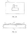
- a preferred overlay capacitor 30is illustrated in FIGS. 2 a , 2 b , 2 c , and 3 that minimizes contributions to L geom .
- the capacitor 30is deposited directly on a 25 mil alumina substrate 31 .
- a first metal layer 34bonds to the substrate 31 .
- the shape of metal layer 34is also illustrated in FIG. 2 b .
- a ferro-electric layer 36overlies the metal layer 34 .
- a metal pad 40 formed on the ferro-electric layer 36overlaps a portion of the first metal layer 34 .
- FIG. 3illustrates an enlarged view of the overlapping portions.
- Both the metal pad 40 and the metal layer 34have a tapering region that forms an overlay capacitor 30 of the appropriate capacitance.
- An additional metal pad 41overlaps the metal layer 34 to form a DC blocking capacitor 42 .
- the metal pad 41is tapered to form an appropriate capacitance for the DC blocking capacitor 42 .
- the overlay capacitor 30may be quite small in area and still provide a capacitance (C f-e ) of 1.5 pF.
- a bonding bias pad 44is provided for attachment of a high value (500-1000 k ⁇ ) chip resistor.
- the f-e filmis deposited not only under the overlay capacitor 30 but also the blocking capacitor 42 .
- the effect on the capacitance (C DC ) of the DC blocking capacitor 42is irrelevant if C DC ⁇ 180 pF and C f-e ⁇ 1.5 pF, even under maximum V DC bias (preferably 10V DC). This is because the DC blocking capacitor has a high enough capacitance that even when the capacitance is reduced by f-e tuning, it still has a minimal effect on C f-e .
- 0.7 ⁇ C f-e ⁇ 1.5 pF, f-e ⁇is approximately 1000
- the overlapped portion of the metal pad 40 forming the overlap capacitor 30is approximately 7.0 ⁇ m ⁇ 7.0 ⁇ m
- the f-e film thicknessis approximately 1.0 ⁇ m.
- the metal layer 34may be Pt and have a thickness of ⁇ 0.5 ⁇ m.
- the metal pads 40 and 41may be Ag and have a thickness of approximately 1.5-2.5 ⁇ m.
- L f-e of an overlay capacitormay be higher, as all of the rf field is concentrated in the f-e film.
- the rf fieldis partially in air, partially in the f-e film and partially in the substrate.
- an overlay capacitorhas greater capacitance tunability for a given applied voltage than a gap capacitor.
- an IDCcan provide a higher capacitance than a gap capacitor. It is more lossy, however, with the main contributions to L geom including the gap spacing; loss increases as the gap spacing decreases. Similarly, loss increases as finger width decreases. The finger length also affects loss with loss increasing as finger length increases; especially in a microstrip (the most common) realization of an IDC as the odd mode loss dominates in such a structure. In addition, loss increases as the number of fingers increases due to loss introduced from the additional sharp corners; note that increasing the number of fingers is typically used to increase the capacitance of an IDC.
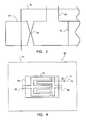
- a preferred IDC capacitor 60is illustrated in FIG. 4 that minimizes the contributions to L geom . It is formed on a 99.5% pure alumina, MgO, sapphire or other suitable substrate 62 of thickness of approximately 0.2 to 1.5 mm. A f-e layer 64 is formed on the substrate 62 . An input port 66 and output port 68 couple to the IDC capacitor 60 . A metal layer 70 having a thickness of 1.5 to 3.0 microns and deposited on the f-e layer 64 forms a gap spacing 72 of approximately 5.0 microns and a finger width 70 of about 150 microns, or greater if possible.
- a general methodology for constructing a tunable bandpass filtermay now be described.
- a designermust tradeoff the 3 dB bandwidth of the tunable filter with filter order to achieve the required out-of-band rejection.
- the rolloffis modeled as beginning at either of the 3 dB points defining the 3 dB bandwidth (BW).
- BW3 dB bandwidth
- the lowest order filteris desired. Typically, this will be a 2 nd order BPF.
- a low order BPFhas a further advantage of being simpler to fabricate and tune, using fewer tunable resonators.
- a Chebychev prototype BPFis preferred over a Butterworth as this gives the designer flexibility to trade off passband ripple with out-of-band rejection.
- the designershould strive to meet the worst case rejection specification by bandwidth adjustment without the addition of extra transmission zeros as transmission zeros increase filter complexity, cost and loss at the corresponding passband edge.
- the narrowest BWshould be chosen that meets the required rejection specification over all specified operating conditions. If the chosen BW provides an unacceptable insertion loss, the BW should be increased, perhaps also requiring an increase in filter order or increased passband ripple (if acceptable). An additional high or low side transmission zero may be added if desired.
- a tunable BPFrequires control circuitry. This is an added expense, not required of fixed-tuned BPF's.
- a desirable tunable filter designshould provide a decreased insertion loss, smaller size, or other benefit over that of a fixed-tuned BPF while meeting rejection specifications, to offset this expense.
- the principles of the inventionmay be advantageously used to design tunable f-e filters of arbitrary order.
- each stage 100is formed by a resonator 102 coupled to a f-e capacitor 104 .
- the f-e capacitor 104may assume one of the forms described herein.
- the resonator 102is shown as a grounded quarter wavelength resonator but an open circuit one-half wavelength resonator may also be used. Moreover, the resonator may be of other suitable electrical length.
- the basic stage 100may be considered a tunable EM resonator.
- the f-e capacitor 104may be coupled either in series or in shunt with the resonator 102 as determined by the nature of their connection. As shown in FIG. 6, the f-e capacitor 104 is coupled in shunt with the resonator 102 such that Q f-e of the f-e capacitor 104 affects the Q of the fix-tuned EM resonator 102 .
- Volumetric resonatorse.g., coaxial, stripline, and monoblock
- Whether a tunable capacitor is placed in series or shunt with a volumetric resonatoris often determined by the case of the connection; sometimes only one placement is even possible.
- Another key feature in determining whether a tunable capacitor is placed in series or shuntis that of minimum added loss and to a lesser extent, tuning range.
- a shunt connectionwill typically produce a more physically compact tunable filter than a series connection. It is usually easier to achieve as well.
- a series connectioncan provide better tuning in the case where electromagnetically coupled resonators (like monoblock, coaxial or stripline) are coupled along their entire extent (rather than coupled through a small aperture).
- a series connectionis a more natural choice in these cases from a fabrication perspective.
- the attachment lossesmay be significant if the f-e capacitor 104 is not integrated with the resonator 102 or other RF circuitry.
- its Q cmay be derived as discussed above.
- Q cis the Q of the f-e capacitor.
- the designermay use equation (1) to determine if the required I.L. will be achieved or exceeded. Should the I.L. be too high, the designer may obtain a lower I.L. by increasing either or both of Q c or Q u . If either Q c or Q u cannot be increased further, they will ultimately limit Q T . Further reduction of I.L. o can then be obtained only by switching to a lower loss topology. For example, Q u may be increased if a volumetric instead of a microstrip resonator is used for a given footprint (area).
- transverse electromagnetic (TEM) wave volumetric resonatorsare preferred.
- volumetric resonatorscan be either ceramic loaded coaxial resonators, slabline (monoblock) or stripline, to name the three most common realizations.
- the standard narrow band (typically defined as a BW ⁇ 10% of f o ) topologycan be realized using top capacitively coupled (TCC) BPF's fabricated with either coaxial or stripline resonators.
- TCCtop capacitively coupled
- Stepped impedance realizations of monoblock BPF'scan be used as well.
- Monoblock resonatorsare typically EM coupled along their entire length, a direct consequence of their design. While they lend themselves to series f-e tuning, shunt tuning can be effectively used as well. Their electrical lengths can be tuned by the selective deposition and patterning of f-e tuning capacitors.
- Non-TEM resonatorscan be used as well, including, but not limited to, dielectric loaded waveguide resonators or dielectric pucks (with or without a shielded enclosure).
- FIG. 11 aThe formation of a “pedestal” on which the f-e capacitors can be optimally integrated as shown in FIG. 11 a for a TCC structure using coaxial resonators as an example.
- the f-e capacitorsare integrated as extensions of the input and output capacitors 315 a and 315 b in FIG. 11 a on the pedestal.
- the f-e capacitorscan be patterned and fabricated on the open ends (faces) (not shown) of the coaxial or monoblock resonators.
- Q cwould have to be increased instead by, for example, replacing an IDC f-e capacitor with a gap or an overlay f-e capacitor.
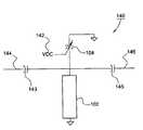
- the bandpass filter 140will include the f-e capacitor 104 and the resonator 102 .
- a variable DC voltage 142 applied to the f-e capacitor 104tunes the filter 140 .
- the RF signal to be filteredis applied at input port 144 and is output at output port 146 . Note that the input port 144 and output port 46 are interchangeable.
- a capacitor 143is defined both between the input port 144 and the resonator 102 .
- Another capacitor 145is defined between the output port 146 and the resonator 102 .
- the f-e capacitor 104regardless of whether it is a gap, overlay, or IDC capacitor, is constructed to minimize losses in the manner described above.
- the resonator 102which may be either a shorted 1 ⁇ 4 wavelength resonator or a 1 ⁇ 2 wavelength open circuit resonator, is selected to maximize Q u .
- a higher Q uwill be provided by a volumetric resonator such as a coaxial resonator, a dielectric loaded waveguide, a monoblock, or a stripline resonator in a smaller footprint and at a lower cost.
- a larger area planar resonatorsuch as a microstrip resonator may be used if specifications and price constraints permit.
- Most microstrip resonator circuitswould be fabricated by thin film process on a hard substrate. As a result, they achieve less metal thickness than TEM resonators like coaxial and monoblock resonators that are metalized by thick film processes.
- Microstrip resonatorsare of larger size since part of the EM field is the air region above the microstrip.
- Resonator 102is formed by a microstrip line 152 grounded through via 154 .
- microstrip line 152could also be terminated in a suitable lossless ground plane (not illustrated), obviating the need for via 154 .
- Capacitors 153 and 155are formed by gaps between the input and output microstrip lines 156 and 158 and the resonator microstrip line 152 . It is desirable to make the capacitance of capacitors 153 and 155 as large, as practical (approximately 0.25 pF) to maximize input and output coupling while still maintaining a planar structure.
- the microstrip linesare formed on substrate 157 of 99.5% pure alumina, MgO, or sapphire that is preferably of thickness approximately 1.0 mm for providing a maximum microstrip resonator Q.
- the f-e capacitor 104is formed as a gap capacitor by pad 160 and mircrostrip line 152 , with f-e layer 162 underneath pad 160 and microstrip line 152 .
- a variable DC voltage sourcebiases pad 160 through resistor 164 .
- a DC blocking capacitoris positioned between pads 160 and 166 , where pad 166 includes a via 168 to ground. Note that pad 166 could also be terminated in a suitable lossless ground plane (not illustrated), obviating the need for via 168 .
- the DC blocking capacitoris needed if the resonator is shunted as shown in FIG. 7 .
- the capacitance of the DC blocking capacitoris ideally at least 100C f-e to minimize its loading effects on C f-e .
- Its Qis ideally ⁇ 40 in the band of interest. It will be appreciated that the choice of a gap capacitor and a microstrip resonator is arbitrary—any of the forms discussed herein could be employed consistent with the teachings of the present invention.
- the bandpass filter of FIG. 7may be ideally used as a test circuit to characterize an f-e film as described herein. As such, the bandpass filter of FIG. 7 provides the following advantages:
- the f-e capacitorcan be fabricated as it is to be used, particularly if that realization is a gap capacitor or IDC. Selective f-e deposition is used.
- a gap capacitorhas a simpler geometry. It is easier to fabricate and has lower geometric loss compared to an IDC. It is also easier to fabricate than an overlay capacitor.
- Metal thicknesscan be accurately measured by profilometry.
- Metal typecan be selected as desired (Au, Ag or Cu).
- a high Q microstrip circuitcompletes the fixed resonator part of the circuit.
- the f-e capacitoris directly fabricated in the resonator. There is no added loss due to soldering, bonding, etc.
- the transition from resonator to f-e capacitoris uniform, or it can be tapered, if desired.
- This circuitcan be fabricated without f-e film to determine a base loss (at a higher f o , of course) of the circuit for correlation to simulations.
- the circuit in FIG. 7can be fabricated with an aperture in the base substrate where the f-e cap is shown. Now, independent f-e caps can be placed over the aperture, held in place with pressure, allowing the f-e caps to be tested as stand-alone components.
- each stage of bandpass filter 400comprises a resonator 404 and 408 and f-e capacitor 410 a and 410 b .
- the resonators 404 and 408are shown as 1 ⁇ 4 wavelength short-circuited resonators but may also be 1 ⁇ 2 wavelength open circuit resonators. In either case, the resonator length is reduced by the presence of C f-e .
- a variable DC voltage applied to the f-e capacitors 410 a and 410 btunes the bandpass filter 400 .
- the ferro-electric capacitors 410 a and 410 bcouple to ground through DC blocking capacitors 412 a and 412 b , since the resonators are shorted in this example.
- An RF signalis received at input port 402 and output at output port 406 .
- input port 402 and output port 406are interchangeable.
- an additional capacitor 432is provided as an impedance or admittance inverter between the resonators 404 and 408 to create the desired BPF response. It will be appreciated that capacitor 432 can also be a discrete element or implemented through aperture coupling between resonators 404 and 408 .
- the tunable two-stage filters 400 and 450 illustrated in FIGS. 8 a and 8 bhave a basic topology which creates a high or low side zero by the addition of electromagnetic coupling along the entire length of resonators 404 and 408 .
- the zerocan be used to provide better rejection for a given passband I.L.
- the passband I.L. and out-of-band rejectionwill change as the ferro-electric capacitors tune the bandpass filter across the passband.
- capacitor 432may be a f-e capacitor. Tuning capacitors 413 and 419 makes the zero track in frequency with the tunable passband.
- capacitor 432may be replaced by f-e capacitors 437 a and 437 b as shown in FIG. 8 b .
- Capacitors 437 a and 437 bideally have a capacitance twice that of capacitor 432 .
- the ferro-electric capacitors 410 a , 410 b , 437 a and 437 bmay all be tuned using a single DC tuning voltage VDC.
- different f-e materialscan be deposited for capacitors 437 a and 437 b than that used for capacitors 410 a and 410 b .
- greater versatilitymay be obtained in tuning with a single voltage.
- the single DC tuning voltage for the f-e capacitorsmay be arranged as shown in FIG. 9 .
- V DCis coupled to a divider network 505 .
- the divider network 505is coupled to both f-e capacitors 437 a and 437 b .
- the divider network 505is configured to provide the appropriate tuning range to the f-e capacitors 437 a and 437 b so as to cause the zero to track with the passband, as described above.
- the divider network 505may be constructed as shown in FIG. 10 .
- V DCis coupled to R 1 .
- R 1is coupled to R 2 and to both capacitors 437 a and 437 b .
- R 2is also coupled to ground.
- R 1 and R 2are chosen to cause the zero to track with the passband, as described above.
- a separate voltagecan be used to tune both capacitors 437 a and 437 b.
- FIG. 11 aa tunable two-stage filter 300 using coaxial, monoblock resonators 302 a and 302 b is illustrated. Note that other resonator types could also be used.
- the resonators 302 a and 302 bmay be open or short circuited.
- the resonators 302 a and 302 battach to a first surface of a substrate 301 . Pads 304 a and 304 b formed on the first surface of the substrate 301 couple to the resonators 302 a and 302 b through leads 305 a and 305 b .
- Pads 306 a and 306 b formed on the first surface of substrate 301couple to pads 304 a and 304 b creating the desired gap for the ferro-electric capacitors 310 a and 310 b .
- Ferro-electric layers 312 a and 312 b underlying the pads 304 a and 304 b and 306 a and 306 bcomplete ferro-electric gap capacitors 310 a and 310 b . Note that the drawings are not to scale. Typically, the gap spacing is increased for clarity.
- transmission lines 320 a and 320 bon a second surface of substrate 301 . These transmission lines are used as input and output ports 320 a and 320 b for signals RF in and RF out.
- the input and output capacitors 315 a and 315 bare formed between the transmission lines 320 a and 320 b and the pads 304 a and 304 b with substrate 301 in between, as shown in FIG. 11 b .
- FIG. 11 bis a cross-sectional view of a portion of filter 300 shown in FIG. 11 a . The cross-section is taken along line B.
- capacitor 321is formed as a gap capacitor by the separation of pads 304 a and 304 b .
- the coupling provided by capacitor 321may alternatively be provided though aperture coupling between coaxial resonators 302 a and 302 b , eliminating the need for capacitor 321 .
- the coaxial resonators 302 a and 302 bare shown as separate structures, they may share a common wall to save space and permit any aperture coupling. Additionally, there may be no space and no wall between them. I.e., they may be mutually coupled monoblock resonators.
- a bias voltage VDCcouples through resistors 340 a and 340 b to tune the ferro-electric capacitors 310 a and 310 b .
- Each of the ferro-electric gap capacitors 310 a and 310 bcouple to ground through DC blocking capacitors 341 a and 341 b.
Landscapes
- Physics & Mathematics (AREA)
- Electromagnetism (AREA)
- Engineering & Computer Science (AREA)
- Power Engineering (AREA)
- Computer Networks & Wireless Communication (AREA)
- Signal Processing (AREA)
- General Physics & Mathematics (AREA)
- Microelectronics & Electronic Packaging (AREA)
- Control Of Motors That Do Not Use Commutators (AREA)
- Waveguide Aerials (AREA)
- Transceivers (AREA)
- Measurement Of Resistance Or Impedance (AREA)
- Semiconductor Integrated Circuits (AREA)
- Inductance-Capacitance Distribution Constants And Capacitance-Resistance Oscillators (AREA)
- Oscillators With Electromechanical Resonators (AREA)
- Filters And Equalizers (AREA)
- Fixed Capacitors And Capacitor Manufacturing Machines (AREA)
- Microwave Amplifiers (AREA)
Abstract
Description
This application claims the benefit of U.S. Provisional Application No. 60/283,093, filed Apr. 11, 2001, titled Low Loss Tunable Ferro-Electric Device and Method of Characterization, which is hereby incorporated by reference.
Filters, such as bandpass filters, have numerous applications in communications and electronics. For example, in wireless communications a given frequency band must accommodate many wireless users. To accommodate so many users, stringent bandpass filtering requirements must be achieved because of the crowded frequency allocations provided.
At present, wireless handsets use fixed-tuned bandpass filters (BPFs) to meet their filtering specifications. The design of such filters is complicated because they must achieve the lowest possible passband insertion loss (I.L.) while simultaneously achieving a specified large out-of-band rejection. As a specific example, consider full band PCS CDMA handsets using fixed bandwidth filters. The PCS transmit (TX) band should have no more than −3.5 dB I.L. in-band (1850 to 1910 MHz in the U.S.) while having at least a 38.0 dB out-of-band rejection in the receive (RX) band (1930 to 1990 MHz range).
Further, this BPF must meet these specifications with a maximum constraint on height. A typical height constraint in present day handsets, for example, is 4.0 mm or less. To meet these demanding electrical requirements yet possess the smallest possible size and height, high order (>2ndorder) fixed-tuned filters constructed from either individual coaxial resonator elements or monoblock structures are usually necessary. In addition, to satisfy out-of-band rejection specifications, a transmission zero is usually required, increasing I.L. at the band edge. Because of variations in ceramics and fabrication tolerances, vendors must individually adjust the characteristics of fixed-tuned filters during their manufacture, driving costs higher.
Moreover, if more than one frequency band were to be supported (e.g., supporting the PCS bands in the U.S., Korea, and India) multiple fixed-tuned BPFs would be necessary, requiring extra switches which introduces additional loss. This is true, even if the power amplifier and low noise amplifier used have sufficient bandwidth to operate over these multiple bands.
A tunable BPF would allow the use of one BPF over several bands, or of a lower order filter to cover a bandwidth wider than a required passband at any particular time. To provide the tunability in a tunable BPF, a component capable of providing a variable capacitance is typically used.
Several structures are presently used to implement a variable capacitor. For example, movable parallel plates have been used for many years as the tuner in home radios. However, such plates are far too bulky, noisy, and impractical for use in most modern applications.
Another alternative, the electronic varactor, is a semiconductor device that adjusts capacitance responsive to an applied voltage. Because the varactor is typically noisy and lossy, particularly in applications above 500 MHz, it is ineffective for high-frequency, low-loss applications where high performance is required.
Another alternative, a micro-electro-mechanical-system (MEMS) is a miniature switching device that may switch between capacitors responsive to an applied control signal. It, however, is costly, difficult to manufacture and of unproven reliability. In most cases, it provides discrete tuning, in that a system must select between a finite (and small) number of fixed capacitors.
Ferroelectric tunable capacitors are another alternative that has been attempted. Ferroelectric (f-e) materials are a class of materials, typically ceramic rare-earth oxides, whose prominent feature is that their dielectric constant (κ), and as a consequence, the electric permittivity (∈) changes in response to an applied slowly varying (DC or low frequency) electric field. The relationship of the dielectric constant (κ) and the electric permittivity (∈) of a material is given as follows:
where ∈0is the electric permittivity of a vacuum. At present, there are several hundred known materials that possess f-e properties. In a typical f-e material, one can obtain a range in κ by a factor of as much as approximately 3:1. The required DC voltage to generate such a change in κ depends on the dimensions of the f-e material over which a DC control voltage is applied. As a result of their variable dielectric constant, one can make tunable capacitors using f-e materials, because the capacitance of a capacitor depends on the dielectric constant of the dielectric proximate the capacitor conductors. Typically, a tunable f-e capacitor is realized as a parallel plate (overlay), interdigital (IDC), or a gap capacitor.
In known f-e variable capacitors, a layer of an appropriate f-e material, such as barium strontium titanate, BaxSr1−xTiO3(BSTO) is disposed adjacent to one or both conductors of a capacitor. Depending upon the strength of the electric field applied to the f-e material and the intrinsic properties of the f-e material selected, the capacitance changes. Typically, below the Curie temperature, Tc, of the f-e film, the f-e material is in the ferroelectric state and will exhibit hysteresis in its response to a changing electric field. Above Tc, f-e material is in the paraelectric state and will not exhibit hysteresis. Thus, one generally picks an f-e material whose Tcis lower than the expected operating temperature so as to operate in the paraelectric state, avoiding the hysteresis effects of the ferroelectric state.
However, conventional f-e variable capacitors have proven to be too lossy for use in insertion-loss-sensitive applications such as handsets. Moreover, these devices often perform unpredictably, preventing optimal design, construction, and use of f-e tunable filters.
Accordingly, there is a need in the art for improved tunable f-e filters capable of providing a tuning range over a desired frequency range with low I.L. and high out-of-band rejections and methods for designing the same.
Fixed tuned bandpass filters must satisfy stringent size, insertion loss and out of band rejection, among other requirements. Tunable filters would be useful in replacing fixed tuned bandpass filters if they could meet these requirements. Lower order, or otherwise better, tunable filters might be used to tune over ranges requiring higher order fixed tuned filters. Or a single tunable filter could replace more than one fixed tuned filter. However, tunable filters require tunable components that have consistently shown themselves to be to high in insertion loss, unreliable, or possessing other prohibitive qualities.
It is desirable to provide a tunable bandpass filter that has superior insertion loss properties with respect to fixed-tuned bandpass filters yet still achieves required rejection performance and satisfies other requirements. It is therefore an object of this invention to provide tunable bandpass filters incorporating ferro-electric materials to tune the filters while maintaining a low insertion loss, meeting stringent out of band rejection requirements and satisfying other requirements. This is made possible by the advantageous design of capacitors and filters based on a correct recognition of the loss characteristics of the ferro-electric materials.
Another object of the invention is to provide a methodology for designing tunable bandpass filters. This methodology quantifies and minimizes loss mechanisms in tunable ferro-electric capacitors to select optimal structures for a tunable bandpass filter incorporating tunable ferro-electric capacitors.
The primary object of this process is to allow the user to design minimum loss BPF's that meet or exceed all other electrical and mechanical specifications placed on a conventional fix-tuned BPF that it replaces. The meeting or exceeding of performance specifications is critical if a tunable BPF is to replace a fix-tuned BPF in practical applications.
Proper f-e film characterization, along with optimum tunable BPF design procedures are mandatory if one is to achieve minimum loss tunable BPF's that simultaneously meet a stringent rejection specification.
In accordance with one embodiment of the invention, a method is provided for choosing a bandwidth and filter order for a tunable bandpass filter to satisfy an out-of-band rejection requirement and a passband insertion loss requirement. Given a topology for a ferro-electric capacitor, the method calculates the non-ferro-electric losses for the ferro-electric capacitor. Given a resonator having a first quality factor for coupling to the ferro-electric capacitor, the method determining the required ferro-electric loss of the f-e capacitor based upon the calculated non-ferro-electric losses and the first quality factor to achieve an insertion loss requirement for the tunable bandpass filter.
In accordance with another embodiment of the invention, a process is described by which a wide variety of f-e films can be efficiently and correctly characterized.
Further aspects and features of the invention are set forth in the following description together with the accompanying drawings.
FIG. 1ais a plan view of a ferro-electric gap capacitor.
FIG. 1bis a cross-sectional view of the ferro-electric gap capacitor of FIG. 1ataken along line A.
FIG. 2ais a plan view of a ferro-electric overlay capacitor, along with an accompanying DC blocking capacitor.
FIG. 2bis a plan view of the first metal layer in the overlay capacitor of FIG. 2a.
FIG. 2cis a cross-sectional view of the overlay capacitor of FIG. 2ataken along line B in FIG. 2a.
FIG. 3 illustrates an enlarged view of area C in FIG. 2a.
FIG. 4 is a plan view of a ferro-electric interdigital capacitor.
FIG. 5 is a schematic of a resonator coupled to a tunable ferro-electric capacitor.
FIG. 6 is a schematic of a single pole tunable filter.
FIG. 7 is a planar circuit implementation of the single pole filter of FIG.6.
FIG. 8ais a schematic of a double pole tunable filter having a ferro-electric capacitor configured to compensate for frequency response distortions induced by tuning.
FIG. 8bis a schematic of a double pole tunable filter having a two ferro-electric capacitors configured to compensate for frequency response distortions induced by tuning.
FIG. 9 is a schematic of a divider network and direct current voltage source used to tune the two ferro-electric capacitors configured to compensate for frequency response distortions induced by tuning shown in FIG. 8b.
FIG. 10 shows one implementation of the divider network shown in FIG.9.
FIG. 11ais a plan view of the tunable filter shown in FIG. 8a.
FIG. 11bis a cross-sectional view of the tunable filter shown in FIG. 11a, taken along line D.
Use of the same reference symbols in different figures indicates similar or identical items.
In designing a tunable bandpass filter (BPF) for use and application in electronic signal processing systems, such as, for example, communications systems, one must usually meet or exceed both out-of-band rejection and pass band insertion loss (I.L.) requirements as well as size, weight and other mechanical, environmental and electrical requirements imposed on fix-tuned BPF's. Further, any such designs targeted for high volume products must be manufacturable and repeatable, with consistent unit-to-unit performance, requiring a minimum (and preferably no) added tuning or testing in-situ.
Thus, for a tunable BPF to be a commercially viable replacement for a fixed-tuned BPF, its performance should exceed that of the fixed-tuned BPF it is replacing in terms of most or all of the electrical and mechanical requirements. In demanding applications such as wireless handsets, passband I.L. must be minimized to prevent placing an even greater burden on other components in the handset. If a tunable BPF has I.L. greater than the fixed-tuned BPF it is to replace, the added I.L. may prove to be too great a burden on the overall system performance.
Many definitions of what defines a “pass band” may be used. Typically the pass band is defined by the points where the bandpass filter response falls to 3.0 dB below the mid-band, or band-center insertion loss (I.L0.). However, any fixed filter response can be used to define the pass band. Higher order (more resonators) bandpass filters are typically required to meet a specific out-of-band rejection requirement. But increasing the filter order will increase the I.L0. A useful basic relationship between filter order, topology and I.L0. is given by the following equation:

where N is the filter order,
Quis the unloaded Q of the resonators used,
Q1=f0/BW (BW is the 3 dB passband and f0is the midband frequency), and
giare the filter element values for a given topology (Chebyshev vs. Butterworth).
Generally, a Chebyshev response is preferable as it gives a steeper rejection response compared to that given by a Butterworth filter for a given filter order. Additionally, increasing the ripple in a Chebychev BPF further increases out of band rejection. As can be seen from equation (1), for a given filter order N, a larger passband results in lower I.L0. as Qlwill decrease as BW increases. This lower I.Lo. comes at the expense of decreased selectivity. To regain selectivity, the filter order N must be increased, at the expense of I.L0. One of ordinary skill in the art of bandpass filter design will appreciate that equation (1) represents the best one can do for a given system requirement and filter order. Using a higher order filter (more resonators of a given unloaded Q) quickly increases I.L0., because the givalues get progressively larger in magnitude, even as there are more of them to sum (increased N). Note that equation (1) neglects implementation losses, which further increase I.L.o, especially as the band edge is approached.
It can be seen from equation (1) that using a first or second order bandpass filter reduces I.L0. At these lower orders, both the number (N) of the gicoefficients decreases as well as the magnitudes of the gi. These low-order filters should be constructed from resonators that have the lowest loss (highest Qu) so as to give the minimum I.L0. possible. The resulting 1stor 2ndorder bandpass filter will always have lower I.L0. for a given resonator size and type (i.e., for a given Qu) than the comparable fixed-tuned bandpass filter design of higher order. Tunability allows the low order narrowband BPF to replace a wider band, fix-tuned BPF. A tunable narrowband low order BPF can cover the entire band of interest, overcoming the limitation of having a narrow bandwidth. This assumes that the desired channel (information) bandwidth is narrower than the total system bandwidth.
Tunable BPFs have the best chance of replacing fixed-tuned BPFs in those cases where the fixed-tuned BPF covers a system bandwidth that is greater than that required for transmission or reception of a single channel. For example, a fixed-tuned BPF in a handset for operation in the U.S. CDMA PCS band covers such a BW. It will be understood that this is also true of U.S. cellular CDMA and many other standards. The techniques, methods and devices taught herein are applicable to many standards besides U.S. CDMA PCS. U.S. CDMA PCS is discussed as an example only.
In the full U.S. PCS band, 60 MHz is allocated for Tx (1850 to 1910 MHz) and 60 MHz for Rx (1930 to 1990 MHz) for full band operation. The CDMA standard is a full duplex system, meaning the handset must simultaneously transmit and receive. To accomplish this, a duplexer filter is needed to separate the bands and prevent interference. While the PCS band is 60 MHz wide, the individual CDMA channel is only 1.25 MHz wide. Current system architecture, however, forces CDMA PCS bandpass filters and multiplexers (including duplexers) to have a BW≧60 MHz as the system must allow for and accommodate operation of any 1.25 MHz channel in any region of the 60 MHz band.
A tunable PCS band filter could alter this situation by meeting the worst case rejection specifications while providing a lower order BPF of simpler topology that occupies a smaller physical area. Such a lower order filter would necessarily provide lower I.L0. by virtue of equation (1). In some circumstances partial band operation, covering a band less than 60 MHz, is desired. Tunable BPF's would be equally advantageous in these circumstances.
To effectively replace a high-order fixed-tuned BPF with a low-order tunable BPF, three factors should be considered. First, the fractional bandwidth (i.e. Q1) of the low-order BPF and the chosen topology must be such that the worst case rejection specification is met. Because Ql=f0/BW, as the 3 dB bandwidth (BW) decreases, the I.L. increases. Thus, if BW is too small relative to f0, the resulting BPF will have an unacceptably high I.L., requiring a tradeoff between BW and I.L. For practical designs, a low-order tunable BPF should have the lowest possible I.L. consistent with meeting the worst-case required rejection. Some topologies are preferred in that they naturally provide a low side (below the transmission band) zero or a high side (above the transmission band) zero.
A topology such as that shown in FIG. 8a, where theresonators capacitor 432. This zero allows for a wider BW to be used, along with a BPF topology of lower ripple (resulting in numerically smaller g1values), thus providing a lower I.L.0as seen in equation (1).
Second, the low-order tunable filter must be tunable to cover the entire BW, just as with a fixed-tuned filter. Finally, the tunable capacitor used within the low-order tunable filter should be of sufficiently low loss so the resulting filter has an I.L. that meets or exceeds specifications. Although a tunable 1stor 2ndorder bandpass filter will be of minimum added loss compared to a higher order (N>2) fixed-tuned bandpass filter design, the tunable component (variable f-e capacitor) must have a fast tuning mechanism and be tunable to cover the entire bandpass range, using the available tuning voltage.
The total loss of a capacitor, Lt, whether tunable or not, is given by a ratio of its dissipated to stored energy, where the energy is stored in the electric field and dissipated in resistance, i.e., Lt=(dissipated energy)/(stored energy). The inverse of this loss is the quality factor, Q=1/Lt.
For a capacitor, Ltmay be given by the quantity (ω*Rs*C), where ω is the frequency in radians, Rsis the total series resistance of the capacitor, and C is the capacitance. This definition of Q is valid for frequencies which are below self resonance due to the reactance of stray inductance associated with any real capacitor and above the frequency at which Rp effectively shunts C, that is, the capacitive reactance is much smaller than Rp. Over this range of frequencies, a real capacitor can be modeled as a resistance Rs in series with the desired capacitance. Thus, Q is inversely proportional to the quantity (ω*Rs*C). For example, as any of the quantities, C, ω and Rsis increased or decreased, all other factors being held constant, Q decreases or increases, respectively. Or, to keep Q constant, if one of the quantities, C, ω, or Rsis decreased or increased the product of the other two quantities must be increased or decreased, respectively.
The importance of determining the total loss given by an f-e capacitor in a resonant circuit can be seen from the following equations: Lc=1/Qcand 1/QT=1/Qc+1/Qu, where,
Lc=the loss of the capacitor;
QT=the total Q of the f-e capacitor and the resonator or inductor combined;
Qc=the Q of the capacitor; and
Qu=the Q of the unloaded resonator or alternatively, the Q of an inductor used to create a parallel resonant circuit.
As Qcincreases, it will affect the QTless and less. If Qcis infinite, it has no affect on QT. For practical purposes, this is also true if Qcis approximately 10*Qu. The converse is true too. As Qubecomes higher and higher relative to Qc, Quhas less and less effect on QT. In either case, the highest practical Qcis desired.
For example, in the PCS band, for a 1.0 pF tunable capacitor to have a Qc=250 at 2.0 GHz requires that Rsbe 0.32 Ω (ohms). This assumes Rp, the parallel resistance, which shunts C, is much greater than Zc, the impedance of the capacitor, at 2.0 GHz (where Rp>about 1.6 kΩ here, for example, as the absolute value of Zc=0.0126 Ω), and that the capacitor self resonant frequency is well above 2.0 GHz, so that the series inductance is negligible. To minimize loss (obtain a low Rs) requires an accounting of all loss mechanisms present and an elimination of these loss mechanisms if possible.
For f-e devices, the total loss is governed by summing each source contribution as follows:
where Lgeomis derived from the topology of the capacitor,
Lattachis loss due to device attachment,
Lmetalis the total metal loss,
Lsubis the base substrate loss (if present),
Lradis the radiation loss, both desired and undesired,
Lmeasis the total loss arising from measurement errors, and
Lf-eis the f-e loss tangent.
This loss allocation can first be used to obtain an accurate value of Lf-e(or f-e tan δ) at the desired operating frequency in the manner in which the f-e capacitor will be used. To correctly derive Lf-e, one must eliminate or constrain all of the other loss contribution sources just described. For example, Lgeomwill vary according to topology, being best for an overlay capacitor, worse for a gap capacitor, and much worse for an IDC capacitor. Although this loss can be reduced and controlled, it is inherent to a device. Consequently, the choice of topology for a given f-e capacitor will affect the best possible Qcattainable from the f-e capacitor. Electromagnetic (EM) software can establish a baseline loss for a desired geometry, assuming a lossless f-e film. This baseline loss represents the best (lowest) loss for a given geometry.
In general, a gap capacitor is easiest to fabricate. An IDC is next easiest, and an overlay capacitor is hardest of these three. Compared to an IDC, the gap capacitor will have a better Q but lower capacitance per unit cross section (W in FIG. 1a). The IDC's capacitance is greater due to the use of a number of fingers per unit cross section. For many communication filter applications, however, large capacitance (C≧4.0 pF) is not needed. Thus, a gap capacitor often can provide adequate capacitance. The inherently high value of κ for most f-e films helps provide relatively high capacitance per unit cross section, W, compared to a conventional gap capacitor.
Lattacharises from discrete device attachment techniques, including, for example, solder, silver paint, or wire bonding. These attachment losses may be large and unpredictable. The lowest losses are achieved by direct fabrication of the f-e capacitor to the resonator or other RF circuitry, thus minimizing if not eliminating this loss component.
The inherent loss of a stand-alone f-e capacitor is of little consequence. What is of much greater consequence is any added loss arising from the attachment of the f-e capacitor to a circuit. Even if the f-e capacitor were lossless, should a large loss connection be used, the overall effect is that of a lossy f-e device. For example, if a Q≧250 at 2.0 GHz is desired for a capacitance of 1.0 pF, then the total series resistance Rsmust be ≦0.32 ohm. Any additional loss will thus further reduce the Q of this capacitor. That this additional loss is external to the actual capacitor is irrelevant. Even unavoidable loss mechanisms, such as those due to mounting, for example, lower the effective Q of the capacitor from the perspective of its effect on the system.
For minimum added loss, the connection between the f-e capacitor and the resonator should provide the lowest added resistance. Thus, the electric currents and charges associated with the f-e capacitor should see a minimum added loss. Conventional bonding or mounting techniques, such as (but not limited to) soldering, wire bonding or silver paint or paste do not provide for such a low loss, controllable bond.
The added, unpredictable loss arising from the use of such bonding methods degrade the realized Q regardless of whether or not the f-e capacitor is being used for resonator tuning purposes or characterization of an f-e film. Thus, for best performance (lowest loss) the f-e capacitor structure should be directly fabricated onto or with the resonator it is meant to tune or onto other essential RF circuitry. Only by direct fabrication can there be a minimum loss transition for electromagnetic (EM) sources (currents) from the f-e tuning elements to the resonator. The desirable effects of direct f-e capacitor fabrication onto or with a resonator can be enhanced by the lack of sharp corners or transitions.
Factors for Lmetalinclude the surface roughness (SR) of the metal, metal thickness as compared to skin depth, δs, and conductivity. SR may be effectively eliminated as a factor if SR is less than aproximately 10 micro inches root mean square (rms) for operating frequencies in the L and S band (1-4 GHz). The metal thickness may be reduced as a factor if the thickness is 1.5 δs or greater, or effectively eliminated if the thickness is ≧5 δs. For electrode contacts, metal thickness (tm) can be approximately 1.5 δs. For the case of electromagnetic resonators, where a travelling or standing wave must be supported, i.e., where the metal in question extends for an appreciable fraction of a wavelength (about 10% or greater), the metal thickness should be closer to about 5 δs or greater.
Conductivity is best for silver, copper and gold (Ag, Cu, and Au, respectively). Thus, Lmetalcan be reduced and controlled, but not eliminated as a factor. Its effect, however, can be calculated by expressions well known to those skilled in the art, or by using line calculator tools available in commonly used circuit simulators, such as Eagleware or Touchstone. Further, precise fabrication control can bound geometric variations in Lmetal.
The loss contribution represented by Lsubmay be minimized by choosing a low loss substrate with a loss tangent less than 0.001 and preferably less than 0.0005 at the operating frequency of interest. Suitable materials include >99% pure alumina, a best current choice for loss/cost benefits. Sapphire or MgO are better than alumina in that they have lower loss tangents, but they are more expensive. All these materials will accept f-e thin films without buffer layers and have a surface roughness that is acceptable with little or no further polishing. Semiconductor substrates are poor choices because of their relatively high conductivity. In addition to the factors of loss tangent, surface roughness and price, suitable substrates should not be brittle, can be fabricated as larger area wafers, and can be easily metallized without extensive preprocessing.
Separating out Lsubfrom the total loss of a composite substrate (f-e film plus substrate) can be achieved by using EM field or circuit simulation software. For example, Sonnet, Momentum, or IE3D may be used. Thus, Lsubcan be reduced significantly and calculated precisely.
Lradcan be eliminated by proper shielding and design, and so is typically not a factor. It should be noted that a wide variety of filters, especially planar filters such as combline or hairpin, depend upon radiative coupling to achieve their desired performance. In these cases, one should ensure that the unwanted, stray coupling is reduced, if not eliminated.
Lmeascan add significantly to the circuit loss error because small, added loss significantly reduces the measured Q of the device-under-test (DUT) or system thus obscuring the intrinsic Q of the DUT. The conventional method for measuring dielectric constant and loss tangent in a material is the cavity perturbation technique, which is well known to anyone skilled in the art. At L-band, however, the size of the cavity becomes quite large. When characterizing thin films (as opposed to bulk) with film thickness ≧1.5 μm, such as f-e films, the problem becomes very difficult as measurement errors can be severe. Furthermore, one should characterize an f-e capacitor (or filter) in a manner most similar to how it will be used. Thus, the preferred way to characterize f-e compounds or films is by microstrip resonator techniques.
For the purposes of determining f-e film characteristics and characterizing f-e capacitors, microstrip techniques are preferred to, for example, stripline or other volumetric techniques for f-e film characterization for the following reasons:
1) Microstrip circuits are planar systems with no substrate as a top cover (which would be a stripline circuit), so no bonding of hard substrates as top covers is required. So there is also no need for continuity of ground planes (top to bottom) as needed in a stripline, for example.
2) Preferably gap capacitors, and alternatively, IDC's, can be readily fabricated and measured.
3) A large body of knowledge exists as to the characterization of microstrip resonators.
4) No complex fixturing or fabrication or both are needed as are required for dielectric cavities, for example.
One should measure high-Q circuits using resonator techniques because broadband measurement may not accurately resolve sub-ohm resistive losses at RF/microwave frequencies with any accuracy. For the same reason, LRC meters are not a good choice.
Measurement at radio frequency is requried to correctly obtain Q, and consequently Rs, for an f-e capacitor, since low frequency measurement, especially those below about 10 to 100 MHz, is dominated by a large parallel resistance, Rp, that shunts the capacitance in question. The dominance of Rp, along with the relatively small values of the capacitance in question (≦4.0 to 5.0 pF) prevents reliable Q (and therefore Rs) measurement at low frequencies.
When used to measure losses, wafer probe stations must be carefully used because it is difficult to calibrate out resistive and inductive loss at RF/microwave frequencies. Probe tips along with their ground connections are also sensitive to placement on the DUT as well as the pressure used to apply them. As a consequence, it is better to use a resonant test circuit that allows for direct measurement of the desired parameters in a way that does not require individual device loss measurements.
Thus, for measurements on resonant circuits, a network analyzer is the preferred choice. To minimize measurement loss and attain the most accurate measurement, one should calibrate out loss to the DUT, perform a full two port calibration of the network analyzer, and use averaging for calibration and measurement. Finally, proper analysis of the measured data, such as that outlined in “Data Reduction Method for Q Measurements of Strip-Line Resonators,” IEEE Transactions in MTT, S. Toncich and R. E. Collin, Vol. 40, No. 9, September 1992, pp. 1833-1836, hereby incorporated by reference, is required to accurately extract the Q, or loss, of the capacitor under test.
Using the results of above discussion to minimize, eliminate, or bound each of the foregoing losses, the total loss may be re-expressed as:
As discussed above, both Lgeomand Lmetalmay be quantified and removed analytically to obtain an accurate measure of Lf-e. Lgeomcan be determined from an accurate electromagnetic simulation of the circuit based on a lossless f-e material assumption. Lmetalcan be determined using the expressions for metal loss assuming conductivity, SR (if applicable), and skin depth. The final term, ΔLmisc, represents a combination of the incomplete removal of the other loss mechanisms or from the finite bounds on or incomplete removal of Lmetaland Lgeomor both. As such it represents an irreducible error term. For accurate measurements of f-e film/component properties, it should be minimized and bounded, as described in the preceding sections.
Finally, to reduce the effect of Lf-eto a minimum one must use selective f-e film deposition to place the f-e film only in regions where it is needed for tuning and nowhere else.
The process of accounting for all loss mechanisms and eliminating or bounding these losses not only determines f-e loss but also establishes correct design guidelines for low-loss tunable filters. Knowledge of Lf-egives the designer a baseline for the f-e film that is necessary for doing any type of optimum design using f-e films. This knowledge is necessary if one is to effectively trade-off loss tangent for tunability, for example. In short, accurate fabrication and measurement techniques result in consistent f-e film loss characterization and application.
Given the above techniques for minimizing loss, preferred embodiments for the three types of f-e capacitors may now be discussed. It will be appreciated, that although these designs are for use in the L band (1-2 GHz), the teachings of the present invention may be used to design f-e capacitors for other frequency bands.
A preferred f-etunable gap capacitor 10 is shown in FIGS. 1aand1bfor use in the cellular band (800 to 1000 MHz) and the L-band (1-2 GHz) for wireless handsets. Thegap capacitor 10 is preferably formed on a ≧99% pure, 0.5 to 1.0 mm thick alumina, MgO, orsapphire substrate 12, having an SR less than a 5.0 micro inch RMS. Alternatively, the gap capacitor can be directly patterned on the front or rear face or a side-wall of any number of resonators structures. Examples are coaxial, monoblock or stripline resonators. Such a capacitor should be fabricated as close to its point of electrical connection to the resonator as possible.
Thesubstrate 12 may have ametal ground plane 14 depending on other requirements. However, the preferred embodiment is without a ground plane to minimize stray capacitance. Preferably, af-e layer 16 of approximately 0.1 to 2.0 microns in thickness formed of BSTO or other suitable or desirable f-e material for maximum capacitance and tuning range is deposited on thesubstrate 12. More preferably,layer 16 is 0.5 to 1.0 microns in thickness. The Ba/Sr fraction, doping, alloying, mixing with other components, and/or annealing determine the desired tuning characteristics and loss (tan δ), and therefore Q also.
Generally, it is preferred that the tuning characteristics meet the minimum required tuning range with the minimum tuning voltage. Preferably, x=0.5 in the BaxSr1−xTiO3composition for room temperature operation, regardless of doping with other elements and pre- or post-process annealing. It will be appreciated that other f-e materials beside BSTO may be used as well. Ametal layer 18 formed on thef-e layer 16 defines agap 20 that is preferentially 3.0 to 5.0 microns wide. Preferably,metal layer 18 is 0.5 to 6.0 microns thick. More preferably,metal layer 18 is 1.5 to 2.5 microns thick. It will be appreciated that thegap 20 can be wider or narrower than this range depending on requirements and processing equipment. For minimum added loss in the PCS band, the resulting capacitance will be approximately 0.6 pF to 1.5 pF at 0 volts DC while for the cellular CDMA band it will be about 1.0 pF to 3.0 pF. The width of the capacitor,W 17, will further determine the f-e capacitance, depending on the particular f-e film used and the desiredgap 20. The width will typically be from 0.25 mm to 2.0 mm. The capacitance is typically 0.6 to 3.0 pF. The resulting capacitor should provide a Q of at least 80 at 2.0 GHz to meet the existing worst case CDMA PCS band BPF loss specification.
To minimize the added loss from the f-e film, selective deposition must be used, i.e., the f-e film is deposited only where needed for tuning and nowhere else as stated above. For example, in thegap capacitor 20 of FIG. 1a, one could deposit the desiredf-e film 16 in a narrow region Df-earound thegap 20, as shown in FIG. 1a. Df-eshould be large enough to ensure that thegap 20 can be repeatedly patterned over the f-e film in manufacturing (allowing for mask alignment tolerance) and to cover the needed area under thegap 20 for tuning purposes. For the L-band PCS filters, Df-e=0.2 to 0.5 mm is adequate with 0.2 mm preferred. As the operating frequency increases Df-ecan decrease. As the operating frequency decreases, Df-ecan increase.
F-E film properties and fabrication will play a significant role in overall capacitor loss. Many techniques exist to mitigate and minimize f-e film loss. One feature of f-e films is that f-e film loss and tunability usually have an inverse relationship. That is, they usually must be traded off against each other. The greater the f-e κ tuning range, the greater the f-e loss in most cases.
Thus, even though f-e materials can achieve a κ tuning range of about 3 to 1, less tuning may be acceptable for a given filter application. In that case, less tuning would be chosen, with the benefit of less loss. For example, in the U.S. PCS CDMA band, the tuning requirement in the transmit band is from 1850 MHz to 1910 MHz, or about 4%. Thus, the f-e material can have significantly less tunability than 3 to 1.
For example, an f-e gap capacitor with 0.6 pF at 0V DC bias, needs to tune 33%, (from 0.6 pF down to 0.4 pF) to tune over the PCS transmit band. The actual tuning range depends on the BPF topology and the band over which the BPF must be tuned. The required tuning voltage to provide the 33% tuning in this example depends on the f-e capacitor geometry, including f-e film thickness, and the f-e film characteristics.
The effect of κ tunability on frequency tunability is determined by the filter topology. This effect must also be considered in choosing an f-e material. But without accurate characterization of the f-e loss to f-e κ tunability trade-off, a designer cannot even begin to choose an optimum f-e material. Accurate characterization of this trade-off allows a designer to choose an optimum f-e material (providing the lowest loss while meeting the tuning requirements).
With respect to Lgeomfor a gap capacitor, the major contributions to loss are the four corners formed by the gap. These losses can be reduced by rounding the corners.
In comparison to gap and interdigital capacitors, an overlay capacitor has the lowest Lgeom. An overlay capacitor is an example of a parallel plate geometry where the plate dimensions (length and width) are much greater than the plate separation. Given such a geometry, most of the electric field between the plates is uniform except for fringing along the edges. The fringing effect can be reduced significantly by the use of a guard band, as is well known in the art. Thus, the geometric loss from a parallel plate capacitor is quite low. In addition, parallel plate geometries can provide high capacitances along with high tuning from small control voltage swings.
Apreferred overlay capacitor 30 is illustrated in FIGS. 2a,2b,2c, and3 that minimizes contributions to Lgeom. Thecapacitor 30 is deposited directly on a 25mil alumina substrate 31. Afirst metal layer 34 bonds to thesubstrate 31. The shape ofmetal layer 34 is also illustrated in FIG. 2b. A ferro-electric layer 36 overlies themetal layer 34. To form theoverlay capacitor 30, ametal pad 40 formed on the ferro-electric layer 36 overlaps a portion of thefirst metal layer 34. FIG. 3 illustrates an enlarged view of the overlapping portions. Both themetal pad 40 and themetal layer 34 have a tapering region that forms anoverlay capacitor 30 of the appropriate capacitance. Anadditional metal pad 41 overlaps themetal layer 34 to form aDC blocking capacitor 42. Themetal pad 41 is tapered to form an appropriate capacitance for theDC blocking capacitor 42.
Due to the high dielectric constant (κ) of the most likely f-e films to be used, theoverlay capacitor 30 may be quite small in area and still provide a capacitance (Cf-e) of 1.5 pF. Abonding bias pad 44 is provided for attachment of a high value (500-1000 kΩ) chip resistor. Note that the f-e film is deposited not only under theoverlay capacitor 30 but also the blockingcapacitor 42. However, the effect on the capacitance (CDC) of theDC blocking capacitor 42 is irrelevant if CDC≧180 pF and Cf-e≦1.5 pF, even under maximum VDCbias (preferably 10V DC). This is because the DC blocking capacitor has a high enough capacitance that even when the capacitance is reduced by f-e tuning, it still has a minimal effect on Cf-e.
In such an embodiment, 0.7≦Cf-e≦1.5 pF, f-e κ is approximately 1000, the overlapped portion of themetal pad 40 forming theoverlap capacitor 30 is approximately 7.0 μm×7.0 μm, and the f-e film thickness is approximately 1.0 μm. Themetal layer 34 may be Pt and have a thickness of ≦0.5 μm. Themetal pads
While the Lgeomof an overlay capacitor is lower than that of a gap capacitor, Lf-eof an overlay capacitor may be higher, as all of the rf field is concentrated in the f-e film. In a gap capacitor the rf field is partially in air, partially in the f-e film and partially in the substrate. For the same reasons, an overlay capacitor has greater capacitance tunability for a given applied voltage than a gap capacitor.
For a given cross sectional area, an IDC can provide a higher capacitance than a gap capacitor. It is more lossy, however, with the main contributions to Lgeomincluding the gap spacing; loss increases as the gap spacing decreases. Similarly, loss increases as finger width decreases. The finger length also affects loss with loss increasing as finger length increases; especially in a microstrip (the most common) realization of an IDC as the odd mode loss dominates in such a structure. In addition, loss increases as the number of fingers increases due to loss introduced from the additional sharp corners; note that increasing the number of fingers is typically used to increase the capacitance of an IDC.
Many investigators in the f-e area have used IDC's with narrow finger widths and gaps (≦5.0 μm for each) to characterize f-e film. This is problematic, as such an IDC structure gives a high Lgeomand therefore a low Q by itself. Typically, Q is much less than 100 at 2.0 GHz for about 1.0 pF, even without any Lf-e. This makes it quite difficult to measure Lf-e. The wide spread use of broad band measurement techniques, as described above, further obfuscates any Lf-emeasurement.
Apreferred IDC capacitor 60 is illustrated in FIG. 4 that minimizes the contributions to Lgeom. It is formed on a 99.5% pure alumina, MgO, sapphire or othersuitable substrate 62 of thickness of approximately 0.2 to 1.5 mm. Af-e layer 64 is formed on thesubstrate 62. Aninput port 66 andoutput port 68 couple to theIDC capacitor 60. Ametal layer 70 having a thickness of 1.5 to 3.0 microns and deposited on thef-e layer 64 forms a gap spacing72 of approximately 5.0 microns and afinger width 70 of about 150 microns, or greater if possible.
A general methodology for constructing a tunable bandpass filter may now be described. As a first step, a designer must tradeoff the 3 dB bandwidth of the tunable filter with filter order to achieve the required out-of-band rejection. As is well known, as the filter order is increased, its rolloff rate increases, making it easier to achieve a required rejection specification. The rolloff is modeled as beginning at either of the 3 dB points defining the 3 dB bandwidth (BW). Thus, as the BW is decreased, it also becomes easier to achieve a required rejection specification.
For minimum loss the lowest order filter is desired. Typically, this will be a 2ndorder BPF. A low order BPF has a further advantage of being simpler to fabricate and tune, using fewer tunable resonators.
A Chebychev prototype BPF is preferred over a Butterworth as this gives the designer flexibility to trade off passband ripple with out-of-band rejection. The designer should strive to meet the worst case rejection specification by bandwidth adjustment without the addition of extra transmission zeros as transmission zeros increase filter complexity, cost and loss at the corresponding passband edge. One can, however, exploit topologies that have naturally occurring high or low side transmission zeros in this case.
Narrowing BW too much, however, will increase the insertion loss, as discussed above. Thus, the narrowest BW should be chosen that meets the required rejection specification over all specified operating conditions. If the chosen BW provides an unacceptable insertion loss, the BW should be increased, perhaps also requiring an increase in filter order or increased passband ripple (if acceptable). An additional high or low side transmission zero may be added if desired.
A tunable BPF requires control circuitry. This is an added expense, not required of fixed-tuned BPF's. Thus, a desirable tunable filter design should provide a decreased insertion loss, smaller size, or other benefit over that of a fixed-tuned BPF while meeting rejection specifications, to offset this expense. To achieve decreased insertion loss and smaller size, it is preferable to use no more than a one or two stage tunable filter. However, it will be appreciated that the principles of the invention may be advantageously used to design tunable f-e filters of arbitrary order.
Given a choice for filter order and BW that satisfies the rejection requirements, the highest possible Qufor a resonator should be used to meet or exceed the required I.L., given size and height constraints. To define Qu, a topology should be chosen for thebasic stage 100 illustrated in FIG.5. Eachstage 100 is formed by aresonator 102 coupled to af-e capacitor 104. Thef-e capacitor 104 may assume one of the forms described herein. Theresonator 102 is shown as a grounded quarter wavelength resonator but an open circuit one-half wavelength resonator may also be used. Moreover, the resonator may be of other suitable electrical length.
Thebasic stage 100 may be considered a tunable EM resonator. Thef-e capacitor 104 may be coupled either in series or in shunt with theresonator 102 as determined by the nature of their connection. As shown in FIG. 6, thef-e capacitor 104 is coupled in shunt with theresonator 102 such that Qf-eof thef-e capacitor 104 affects the Q of the fix-tunedEM resonator 102. Volumetric resonators (e.g., coaxial, stripline, and monoblock) are preferred, as they provide the highest Quand smallest area and height at a minimal price compared to planar, i.e., microstrip or coplanar waveguide (CPW) alternatives.
Whether a tunable capacitor is placed in series or shunt with a volumetric resonator is often determined by the case of the connection; sometimes only one placement is even possible. Another key feature in determining whether a tunable capacitor is placed in series or shunt is that of minimum added loss and to a lesser extent, tuning range. A shunt connection will typically produce a more physically compact tunable filter than a series connection. It is usually easier to achieve as well. A series connection can provide better tuning in the case where electromagnetically coupled resonators (like monoblock, coaxial or stripline) are coupled along their entire extent (rather than coupled through a small aperture). A series connection is a more natural choice in these cases from a fabrication perspective.
As discussed above, the attachment losses may be significant if thef-e capacitor 104 is not integrated with theresonator 102 or other RF circuitry. Once a topology for thef-e capacitor 104 is chosen, its Qcmay be derived as discussed above. QTfor the overallbasic stage 100 is then given by 1/QT=1/Qc+1/Qu,
where Quis the unloaded Q of theresonator 102;
and Qcis the Q of the f-e capacitor.
Given the QTfor thebasic stage 100, the designer may use equation (1) to determine if the required I.L. will be achieved or exceeded. Should the I.L. be too high, the designer may obtain a lower I.L. by increasing either or both of Qcor Qu. If either Qcor Qucannot be increased further, they will ultimately limit QT. Further reduction of I.L.ocan then be obtained only by switching to a lower loss topology. For example, Qumay be increased if a volumetric instead of a microstrip resonator is used for a given footprint (area).
For high volume applications, such as CDMA wireless handsets, transverse electromagnetic (TEM) wave volumetric resonators are preferred. Such volumetric resonators can be either ceramic loaded coaxial resonators, slabline (monoblock) or stripline, to name the three most common realizations. The standard narrow band (typically defined as a BW≦10% of fo) topology can be realized using top capacitively coupled (TCC) BPF's fabricated with either coaxial or stripline resonators. The TCC topology as shown in FIG. 8, lends itself to shunt f-e tuning, as this provides the most compact realization (having a smaller footprint than a TCC topology with series f-e tuning). Since grounded quarter wave resonators behave as parallel LC tuned circuits near resonance, placing an f-e tuning capacitor in shunt is advantageous.
Stepped impedance realizations of monoblock BPF's can be used as well. Monoblock resonators are typically EM coupled along their entire length, a direct consequence of their design. While they lend themselves to series f-e tuning, shunt tuning can be effectively used as well. Their electrical lengths can be tuned by the selective deposition and patterning of f-e tuning capacitors. Non-TEM resonators can be used as well, including, but not limited to, dielectric loaded waveguide resonators or dielectric pucks (with or without a shielded enclosure).
However, height restrictions may limit the achievable Qufrom volumetric resonators. An alternative to a volumetric coaxial resonator in such height-constrained systems is to use a stripline resonator. Here, one can make the center conductor wider (up to a point) thus improving Quwhile keeping the total height fixed. This embodiment has further merit in that the incorporation of a planar f-e capacitor such as a gap capacitor or IDC can be realized efficiently by making the top cover of the stripline resonator end before the location of the f-e capacitor. In this manner, the planar f-e capacitor would be formed on the portion of the substrate forming the bottom cover of the stripline resonator that extends beyond the top cover.
The formation of a “pedestal” on which the f-e capacitors can be optimally integrated as shown in FIG. 11afor a TCC structure using coaxial resonators as an example. The f-e capacitors are integrated as extensions of the input andoutput capacitors
Regardless of the particular resonator being implemented, if height restrictions prevent any further increase in the Quof the resonator, Qcwould have to be increased instead by, for example, replacing an IDC f-e capacitor with a gap or an overlay f-e capacitor.
For many applications a singlestage bandpass filter 140 will be satisfactory as illustrated in FIG.6. As discussed with respect to FIG. 5, thebandpass filter 140 will include thef-e capacitor 104 and theresonator 102. Avariable DC voltage 142 applied to thef-e capacitor 104 tunes thefilter 140. The RF signal to be filtered is applied atinput port 144 and is output atoutput port 146. Note that theinput port 144 and output port46 are interchangeable. Acapacitor 143 is defined both between theinput port 144 and theresonator 102. Anothercapacitor 145 is defined between theoutput port 146 and theresonator 102. Thef-e capacitor 104, regardless of whether it is a gap, overlay, or IDC capacitor, is constructed to minimize losses in the manner described above. Similarly, theresonator 102, which may be either a shorted ¼ wavelength resonator or a ½ wavelength open circuit resonator, is selected to maximize Qu.
A higher Quwill be provided by a volumetric resonator such as a coaxial resonator, a dielectric loaded waveguide, a monoblock, or a stripline resonator in a smaller footprint and at a lower cost. Alternatively, a larger area planar resonator such as a microstrip resonator may be used if specifications and price constraints permit. Most microstrip resonator circuits would be fabricated by thin film process on a hard substrate. As a result, they achieve less metal thickness than TEM resonators like coaxial and monoblock resonators that are metalized by thick film processes. Microstrip resonators are of larger size since part of the EM field is the air region above the microstrip.
Turning now to FIG. 7, aplanar realization 150 of thebandpass filter 140 is illustrated.Resonator 102 is formed by amicrostrip line 152 grounded through via154. Note thatmicrostrip line 152 could also be terminated in a suitable lossless ground plane (not illustrated), obviating the need for via154.Capacitors output microstrip lines resonator microstrip line 152. It is desirable to make the capacitance ofcapacitors substrate 157 of 99.5% pure alumina, MgO, or sapphire that is preferably of thickness approximately 1.0 mm for providing a maximum microstrip resonator Q. Thef-e capacitor 104 is formed as a gap capacitor bypad 160 andmircrostrip line 152, withf-e layer 162 underneathpad 160 andmicrostrip line 152.
A variable DC voltage source biases pad160 throughresistor 164. A DC blocking capacitor is positioned betweenpads pad 166 includes a via168 to ground. Note thatpad 166 could also be terminated in a suitable lossless ground plane (not illustrated), obviating the need for via168.
The DC blocking capacitor is needed if the resonator is shunted as shown in FIG.7. The capacitance of the DC blocking capacitor is ideally at least 100Cf-eto minimize its loading effects on Cf-e. Its Q is ideally ≧40 in the band of interest. It will be appreciated that the choice of a gap capacitor and a microstrip resonator is arbitrary—any of the forms discussed herein could be employed consistent with the teachings of the present invention.
The bandpass filter of FIG. 7 may be ideally used as a test circuit to characterize an f-e film as described herein. As such, the bandpass filter of FIG. 7 provides the following advantages:
1) The f-e capacitor can be fabricated as it is to be used, particularly if that realization is a gap capacitor or IDC. Selective f-e deposition is used.
2) While an f-e gap capacitor is shown, an IDC could be used as well. A gap capacitor has a simpler geometry. It is easier to fabricate and has lower geometric loss compared to an IDC. It is also easier to fabricate than an overlay capacitor.
3) Since the circuit is fabricated with thin film processing techniques the geometry can be precisely controlled and measured.
4) Metal thickness can be accurately measured by profilometry. Metal type can be selected as desired (Au, Ag or Cu).
5) A high Q microstrip circuit completes the fixed resonator part of the circuit.
6) The f-e capacitor is directly fabricated in the resonator. There is no added loss due to soldering, bonding, etc. The transition from resonator to f-e capacitor is uniform, or it can be tapered, if desired.
7) No via holes are needed if large area ground planes and a Wiltron test fixture (with jaws to hold and ground the circuit top and bottom) is used. Drilling vias in hard substrates is a significant cost adder and reduces the number of such test circuits that can be fabricated.
8) This circuit can be accurately modeled in EM software.
9) This circuit can be fabricated without f-e film to determine a base loss (at a higher fo, of course) of the circuit for correlation to simulations.
10) The use of a low loss substrate minimizes its effect on the overall circuit.
11) Measured results of foand I.Lo. can be used to extract f-e film dielectric constant and tan δ.
12) The circuit in FIG. 7 can be fabricated with an aperture in the base substrate where the f-e cap is shown. Now, independent f-e caps can be placed over the aperture, held in place with pressure, allowing the f-e caps to be tested as stand-alone components.
Referring now to FIG. 8a, a two stage TCCtunable BPF 400 is illustrated. As discussed with respect to FIG. 5, each stage ofbandpass filter 400 comprises aresonator f-e capacitor resonators
A variable DC voltage applied to thef-e capacitors bandpass filter 400. The ferro-electric capacitors DC blocking capacitors
An RF signal is received atinput port 402 and output atoutput port 406. Note thatinput port 402 andoutput port 406 are interchangeable. In addition toinput capacitor 434aandoutput capacitor 434b, which are functionally similar tocapacitors additional capacitor 432 is provided as an impedance or admittance inverter between theresonators capacitor 432 can also be a discrete element or implemented through aperture coupling betweenresonators
The tunable two-stage filters resonators capacitor 432 may be a f-e capacitor. Tuning capacitors413 and419 makes the zero track in frequency with the tunable passband.
To facilitate the biasing and tuning of f-e capacitor coupling between theresonators capacitor 432 may be replaced byf-e capacitors Capacitors capacitor 432. In this embodiment, the ferro-electric capacitors capacitors capacitors
The single DC tuning voltage for the f-e capacitors may be arranged as shown in FIG.9. In FIG. 9, VDCis coupled to adivider network 505. Thedivider network 505 is coupled to bothf-e capacitors divider network 505 is configured to provide the appropriate tuning range to thef-e capacitors
Thedivider network 505 may be constructed as shown in FIG.10. In FIG. 10, VDCis coupled to R1. R1is coupled to R2and to bothcapacitors
Alternatively, a separate voltage can be used to tune bothcapacitors
Turning now to FIG. 11a, a tunable two-stage filter 300 using coaxial,monoblock resonators resonators resonators substrate 301.Pads substrate 301 couple to theresonators leads Pads substrate 301 couple topads electric capacitors electric layers pads electric gap capacitors
There aretransmission lines substrate 301. These transmission lines are used as input andoutput ports output capacitors transmission lines pads substrate 301 in between, as shown in FIG.11b. FIG. 11bis a cross-sectional view of a portion offilter 300 shown in FIG. 11a. The cross-section is taken along line B.
In addition,capacitor 321 is formed as a gap capacitor by the separation ofpads capacitor 321 may alternatively be provided though aperture coupling betweencoaxial resonators capacitor 321. It will be appreciated that although thecoaxial resonators capacitor 321 is implemented through aperture coupling, thepads resistors electric capacitors electric gap capacitors DC blocking capacitors
Although the invention has been described with reference to particular embodiments, the description is only an example of the invention's application and should not be taken as a limitation. Consequently, various adaptations and combinations of features of the embodiments disclosed are within the scope of the invention as encompassed by the following claims.
Claims (23)
1. A tunable electromagnetic signal filter comprising:
a dielectric constant adjustment signal generator for generating a dielectric constant adjustment signal;
an element having a capacitance and a quality factor;
a volumetric resonator;
the element and the resonator configured as an electromagnetic signal filter having a resonant frequency;
a ferro-electric material positioned proximate the first element for adjusting, responsive to the dielectric constant adjustment signal, the capacitance of the first element for adjusting the resonant frequency; and
wherein the quality factor, when operated in a temperature range between about −50 degrees Celsius and 100 degrees Celsius, is greater than about 180 in a frequency range between 0.25 GHz and 7.0 GHz.
2. A tunable electromagnetic signal filter comprising:
a dielectric constant adjustment signal generator for generating a dielectric constant adjustment signal;
a first element having a capacitance;
a second element having an inductance;
the first and second elements configured as an electromagnetic signal filter having a resonant frequency;
a ferro-electric material positioned proximate the first element for adjusting, responsive to the dielectric constant adjustment signal, the capacitance of the first element for adjusting the resonant frequency;
wherein a quality factor of the first element, when operated in a temperature range between about −50 degrees Celsius and 100 degrees Celsius, is greater than about 80; and
further comprising an overlay capacitor comprising:
a substrate;
a first metal layer on a first surface of the substrate,
a second metal layer, and
a ferro-electric layer disposed between the first and second metal layers, wherein the ferro-electric layer has a thickness of approximately 1 micron, the first metal layer has a thickness of less than approximately 0.5 micron and the second metal layer has a thickness of between approximately 1.5 to 2.5 microns.
3. A tunable electromagnetic signal filter comprising:
a dielectric constant adjustment signal generator for generating a dielectric constant adjustment signal;
a first element having a capacitance;
a second element having an inductance;
the first and second elements configured as an electromagnetic signal filter having a resonant frequency;
a ferro-electric material positioned proximate the first element for adjusting, responsive to the dielectric constant adjustment signal, the capacitance of the first element for adjusting the resonant frequency;
wherein a quality factor of the first element, when operated in a temperature range between about −50 degrees Celsius and 100 degrees Celsius, is greater than about 80; and
wherein the quality factor, when operated in a temperature range between about −50 degrees Celsius and 100 degrees Celsius, is greater than about 80 in a frequency range between 0.25 GHz and 7.0 GHz.
4. A tunable electromagnetic signal filter comprising:
a dielectric constant adjustment signal generator for generating a dielectric constant adjustment signal;
an element having a capacitance and a quality factor;
a volumetric resonator;
the element and the resonator configured as an electromagnetic signal filter having a resonant frequency;
a ferro-electric material positioned proximate the first element for adjusting, responsive to the dielectric constant adjustment signal, the capacitance of the first element for adjusting the resonant frequency; and
wherein the quality factor, when operated in a temperature range between about −50 degrees Celsius and 100 degrees Celsius, is greater than about 80 in a frequency range between 0.25 GHz and 7.0 GHz.
5. A tunable electromagnetic signal filter comprising:
a dielectric constant adjustment signal generator for generating a dielectric constant adjustment signal;
an element having a capacitance and a quality factor;
a volumetric resonator;
the element and the resonator configured as an electromagnetic signal filter having a resonant frequency;
a ferro-electric material positioned proximate the first element for adjusting, responsive to the dielectric constant adjustment signal, the capacitance of the first element for adjusting the resonant frequency; and
further comprising an overlay capacitor comprising:
a substrate;
a first metal layer on a first surface of the substrate,
a second metal layer, and
a ferro-electric layer disposed between the first and second metal layers, wherein the ferro-electric layer has a thickness of approximately 1 micron, the first metal layer has a thickness of less than approximately 0.5 micron and the second metal layer has a thickness of between approximately 1.5 to 2.5 microns.
6. The filter ofclaim 1 or4 wherein the quality factor, when operated in a temperature range between about −50 degrees Celsius and 100 degrees Celsius, is greater than about 80 in a frequency range between about 0.8 GHz and 7.0 GHz.
7. The filter ofclaim 6 , wherein the quality factor, when operated in a temperature range between about −50 degrees Celsius and 100 degrees Celsius, is greater than about 80 in a frequency range between about 0.25 GHz and 2.5 GHz.
8. The filter ofclaim 7 , wherein the quality factor, when operated in a temperature range between about −50 degrees Celsius and 100 degrees Celsius, is greater than about 80 in a frequency range between about 0.8 GHz and 2.5 GHz.
9. A tunable electromagnetic signal filter comprising:
a dielectric constant adjustment signal generator for generating a dielectric constant adjustment signal;
a first element having a capacitance;
a second element having an inductance;
the first and second elements configured as an electromagnetic signal filter having a resonant frequency;
a ferro-electric material positioned proximate the first element for adjusting, responsive to the dielectric constant adjustment signal, the capacitance of the first element for adjusting the resonant frequency;
wherein a quality factor of the first element, when operated in a temperature range between about −50 degrees Celsius and 100 degrees Celsius, is greater than about 80; and
wherein the quality factor, when operated in a temperature range between about −50 degrees Celsius and 100 degrees Celsius, is greater than about 180 in a frequency range between 0.25 GHz and 7.0 GHz.
10. The filter ofclaim 3 or4 , wherein the quality factor, when operated in a temperature range between about −50 degrees Celsius and 100 degrees Celsius, is greater than about 180 in a frequency range between about 0.8 GHz and 2.5 GHz.
11. A method of designing a tunable bandpass filter, comprising:
choosing a bandwidth and filter order to satisfy an out-of-band rejection and passband insertion loss requirement;
choosing a topology for a ferro-electric capacitor;
calculation the non-ferro-electric losses for the chosen topology;
choosing a resonator having a first quality factor for coupling to the f-e capacitor; and
determining, based upon the calculated non-ferro-electric losses and first quality factor, the required ferro-electric loss of the ferro-electric capacitor to satisfy the insertion loss requirement for the tunable filter.
12. The method ofclaim 11 , wherein the topology chosen for the f-e capacitor is a gap capacitor.
13. The method ofclaim 11 , wherein the topology chosen for the f-e capacitor is an overlay capacitor.
14. The method ofclaim 11 , wherein the topology chosen for the f-e capacitor is an IDC capacitor.
15. A tunable electromagnetic signal filter comprising:
a dielectric constant adjustment signal generator for generating a dielectric constant adjustment signal;
a first element having a capacitance;
a second element having an inductance;
the first and second elements configured as an electromagnetic signal filter having a resonant frequency;
a ferro-electric material positioned proximate the first element for adjusting, responsive to the dielectric constant adjustment signal, the capacitance of the first element for adjusting the resonant frequency;
wherein a quality factor of the first element, when operated in a temperature range between about −50 degrees Celsius and 100 degrees Celsius, is greater than about 80; and
further comprising a gap capacitor comprising:
a substrate;
a metal layer on a first surface of the substrate, the metal layer defining the gap;
a ferro-electric layer between the metal layer and the substrate; and wherein:
the substrate is a low loss material having a thickness between approximately 0.5 and 1.0 mm;
the metal layer is formed to have a surface roughness less than approximately 5.0 micro inch; and
the gap spacing of the gap defined by the metal layer is approximately 3.0 to 5.0 microns.
16. A tunable electromagnetic signal filter comprising:
a dielectric constant adjustment signal generator for generating a dielectric constant adjustment signal;
an element having a capacitance and a quality factor;
a volumetric resonator;
the element and the resonator configured as an electromagnetic signal filter having a resonant frequency;
a ferro-electric material positioned proximate the first element for adjusting, responsive to the dielectric constant adjustment signal, the capacitance of the first element for adjusting the resonant frequency; and
further comprising a gap capacitor comprising:
a substrate;
a metal layer on a first surface of the substrate, the metal layer defining the gap;
a ferro-electric layer between the metal layer and the substrate; and wherein:
the substrate is a low loss material having a thickness between approximately 0.5 and 1.0 mm;
the metal layer is formed to have a surface roughness less than approximately 5.0 micro inch; and
the gap spacing of the gap defined by the metal layer is approximately 3.0 to 5.0 microns.
17. The filter ofclaim 15 or16 , wherein the gap capacitor comprises metal lines having a width of approximately 0.25 mm to 2.0 mm.
18. The filter ofclaim 15 or16 , wherein the ferro-electric material is localized in the area of the gap.
19. The filter ofclaim 18 , wherein the ferro-electric material is contained within about 2.0 microns of the gap.
20. The filter ofclaim 15 or16 , wherein the metal lines defining the gap have rounded corners.
21. The filter ofclaim 15 or16 , wherein the low loss material is selected from the group consisting of magnesium oxide, sapphire, and at least 99% pure alumina.
22. The filter ofclaim 15 or16 , wherein the metal layer has a thickness of approximately 1.5 to 2.5 microns and the ferro-electric material comprises barium strontium titanate having a thickness of approximately 0.5 to 1.0 microns.
23. A tunable electromagnetic signal filter comprising:
a dielectric constant adjustment signal generator for generating a dielectric constant adjustment signal;
an element having a capacitance and a quality factor;
a volumetric resonator;
the element and the resonator configured as an electromagnetic signal filter having a resonant frequency;
a ferro-electric material positioned proximate the first element for adjusting, responsive to the dielectric constant adjustment signal, the capacitance of the first element for adjusting the resonant frequency; and
wherein the resonator comprises a coaxial dielectric loaded resonator.
Priority Applications (90)
| Application Number | Priority Date | Filing Date | Title |
|---|---|---|---|
| US09/904,631US6690251B2 (en) | 2001-04-11 | 2001-07-13 | Tunable ferro-electric filter |
| ES02722534TES2315361T3 (en) | 2001-04-11 | 2002-04-02 | ADJUSTABLE ADAPTATION CIRCUIT. |
| EP02722535AEP1382083B1 (en) | 2001-04-11 | 2002-04-02 | Tunable multiplexer |
| PCT/IB2002/001026WO2002087082A1 (en) | 2001-04-11 | 2002-04-02 | Tunable matching circuit |
| CNB028107446ACN100419440C (en) | 2001-04-11 | 2002-04-02 | Method for determining ferroelectric element induced wear |
| EP02716979AEP1377994B1 (en) | 2001-04-11 | 2002-04-02 | Tunable ferro-electric filter |
| KR1020037013374AKR100798616B1 (en) | 2001-04-11 | 2002-04-02 | Tuned Multiplexer |
| KR1020037013373AKR100976339B1 (en) | 2001-04-11 | 2002-04-02 | Tuned Ferroelectric Filter |
| DE60228430TDE60228430D1 (en) | 2001-04-11 | 2002-04-02 | TUNABLE ADJUSTMENT |
| AT02722534TATE405986T1 (en) | 2001-04-11 | 2002-04-02 | TUNABLE ADJUSTABLE CIRCUIT |
| PCT/IB2002/001027WO2002084310A1 (en) | 2001-04-11 | 2002-04-02 | Low-loss tunable ferro-electric device and method of characterization |
| CN2010101292437ACN101800522B (en) | 2001-04-11 | 2002-04-02 | Tunable ferro-electric filter |
| EP02718436AEP1377839B1 (en) | 2001-04-11 | 2002-04-02 | Low-loss tunable ferro-electric device and method of characterization |
| CNB028113454ACN1294673C (en) | 2001-04-11 | 2002-04-02 | Tuning multiplexer |
| DE60230498TDE60230498D1 (en) | 2001-04-11 | 2002-04-02 | TUNABLE MULTIPLEXER |
| CNB028111672ACN100557738C (en) | 2001-04-11 | 2002-04-02 | Tunable ferroelectric filter |
| KR1020037013372AKR100942134B1 (en) | 2001-04-11 | 2002-04-02 | Low-loss tunable ferro-electric device and method of characterization |
| PCT/IB2002/001028WO2002084685A1 (en) | 2001-04-11 | 2002-04-02 | Tunable ferro-electric filter |
| ES02718436TES2252442T3 (en) | 2001-04-11 | 2002-04-02 | FERO-ELECTRIC DEVICE, ADJUSTABLE WITH LOW LOSSES AND CHARACTERIZATION METHOD. |
| CN201010129230XACN101814903B (en) | 2001-04-11 | 2002-04-02 | Tunable ferro-electric filter |
| EP02722534AEP1380106B1 (en) | 2001-04-11 | 2002-04-02 | Tunable matching circuit |
| DE60207697TDE60207697T2 (en) | 2001-04-11 | 2002-04-02 | TUNABLE FERROELECTRIC ELEMENT WITH LOW LOSSES AND METHOD FOR THE CHARACTERIZATION THEREOF |
| AT02718436TATE311606T1 (en) | 2001-04-11 | 2002-04-02 | LOW LOSS TUNABLE FERROELECTRIC ELEMENT AND METHOD FOR CHARACTERIZING SAME |
| JP2002582012AJP2004536287A (en) | 2001-04-11 | 2002-04-02 | Low loss tunable ferroelectric device and method of characterization |
| AT02716979TATE483238T1 (en) | 2001-04-11 | 2002-04-02 | TUNABLE FERRO-ELECTRIC FILTER |
| JP2002584476AJP2004524778A (en) | 2001-04-11 | 2002-04-02 | Tunable matching circuit |
| JP2002581541AJP4077322B2 (en) | 2001-04-11 | 2002-04-02 | Tunable ferroelectric filter |
| ES02722535TES2319106T3 (en) | 2001-04-11 | 2002-04-02 | TUNING MULTIPLEXOR. |
| CN2007101357923ACN101136618B (en) | 2001-04-11 | 2002-04-02 | Tunable ferro-electric filter |
| PCT/IB2002/001030WO2002084781A1 (en) | 2001-04-11 | 2002-04-02 | Tunable multiplexer |
| JP2002581616AJP2004530360A (en) | 2001-04-11 | 2002-04-02 | Tunable multiplexer |
| AT02722535TATE418801T1 (en) | 2001-04-11 | 2002-04-02 | TUNABLE MULTIPLEXER |
| DE60237808TDE60237808D1 (en) | 2001-04-11 | 2002-04-02 | TUNABLE FERRO ELECTRIC FILTER |
| EP02722541AEP1384281B1 (en) | 2001-04-11 | 2002-04-04 | Antenna interface unit |
| PCT/IB2002/001077WO2002084782A2 (en) | 2001-04-11 | 2002-04-04 | Antenna interface unit |
| JP2002581617AJP4216080B2 (en) | 2001-04-11 | 2002-04-04 | Antenna interface unit |
| AT02718438TATE364916T1 (en) | 2001-04-11 | 2002-04-04 | FERROELECTRIC ANTENNA AND METHOD FOR TUNING SAME |
| DE60207546TDE60207546T2 (en) | 2001-04-11 | 2002-04-04 | ANTENNA INTERFACE UNIT |
| KR1020037013377AKR101110382B1 (en) | 2001-04-11 | 2002-04-04 | Ferroelectric antenna and method for tuning same |
| AT02722541TATE311018T1 (en) | 2001-04-11 | 2002-04-04 | ANTENNA INTERFACE UNIT |
| EP06123190AEP1753084B1 (en) | 2001-04-11 | 2002-04-04 | Ferroelectric slot antenna |
| PCT/IB2002/001087WO2002084788A1 (en) | 2001-04-11 | 2002-04-04 | Tunable antenna matching circuit |
| PCT/IB2002/001078WO2002087016A1 (en) | 2001-04-11 | 2002-04-04 | Ferroelectric antenna and method for tuning same |
| EP02718438AEP1384285B1 (en) | 2001-04-11 | 2002-04-04 | Ferroelectric antenna and method for tuning same |
| JP2002584427AJP2005502227A (en) | 2001-04-11 | 2002-04-04 | Ferroelectric antenna and method for adjusting the same |
| DE60220664TDE60220664T2 (en) | 2001-04-11 | 2002-04-04 | FERROELECTRIC ANTENNA AND METHOD OF VOTING THEREOF |
| ES02718438TES2287264T3 (en) | 2001-04-11 | 2002-04-04 | RAILWAY ANTENNA AND METHOD TO TUNE IT. |
| ES02722541TES2252445T3 (en) | 2001-04-11 | 2002-04-04 | ANTENNA INTERFACE UNIT. |
| PCT/IB2002/001082WO2002084783A1 (en) | 2001-04-11 | 2002-04-05 | Tunable isolator |
| PCT/IB2002/001098WO2002084869A1 (en) | 2001-04-11 | 2002-04-05 | Tunable power amplifier matching circuit |
| PCT/IB2002/001097WO2002084684A2 (en) | 2001-04-11 | 2002-04-05 | Tunable planar capacitor |
| PCT/IB2002/001086WO2002084868A1 (en) | 2001-04-11 | 2002-04-05 | Tunable impedance matching circuit |
| AU2002249507AAU2002249507A1 (en) | 2001-04-11 | 2002-04-05 | Tunable planar capacitor |
| AT02718443TATE415734T1 (en) | 2001-04-11 | 2002-04-08 | TUNABLE VOLTAGE CONTROLLED OSCILLATOR |
| DE60230030TDE60230030D1 (en) | 2001-04-11 | 2002-04-08 | TUNABLE VOLTAGE CONTROLLED OSCILLATOR |
| PCT/IB2002/001107WO2002084857A1 (en) | 2001-04-11 | 2002-04-08 | Tunable voltage controlled oscillator |
| EP02718443AEP1384312B1 (en) | 2001-04-11 | 2002-04-08 | Tunable voltage controlled oscillator |
| ES02718443TES2314045T3 (en) | 2001-04-11 | 2002-04-08 | TENSION CONTROLLED OSCILLATOR AND TUNING. |
| JP2002581679AJP4666564B2 (en) | 2001-04-11 | 2002-04-08 | Tunable voltage controlled oscillator |
| PCT/IB2002/001119WO2002084858A1 (en) | 2001-04-11 | 2002-04-09 | Tunable voltage-controlled temperature-compensated crystal oscillator |
| EP02718445AEP1384286B9 (en) | 2001-04-11 | 2002-04-09 | Inverted-f ferroelectric antenna |
| JP2002581630AJP4452444B2 (en) | 2001-04-11 | 2002-04-09 | Inverted F ferroelectric antenna |
| ES02718445TES2265493T3 (en) | 2001-04-11 | 2002-04-09 | FERROELECTRICA ANTENA INVESTED IN F. |
| PCT/IB2002/001120WO2002084798A1 (en) | 2001-04-11 | 2002-04-09 | Inverted-f ferroelectric antenna |
| DE60212370TDE60212370T2 (en) | 2001-04-11 | 2002-04-09 | INVERTED-F FERROELECTRIC ANTENNA |
| AT02718445TATE330340T1 (en) | 2001-04-11 | 2002-04-09 | INVERTED-F FERROELECTRIC ANTENNA |
| JP2002581614AJP4031367B2 (en) | 2001-04-11 | 2002-04-10 | Tunable phase shifter and applications for it |
| AT02720351TATE338351T1 (en) | 2001-04-11 | 2002-04-10 | TUNABLE PHASE SHIFTER AND APPLICATIONS THEREOF |
| EP02720351AEP1393403B1 (en) | 2001-04-11 | 2002-04-10 | Tunable phase shifter and applications for same |
| ES02720351TES2269673T3 (en) | 2001-04-11 | 2002-04-10 | VARIATOR OF TUNING PHASE AND APPLICATIONS OF THE SAME. |
| DE60214368TDE60214368T2 (en) | 2001-04-11 | 2002-04-10 | TUNABLE PHASE SLIDER AND APPLICATIONS THEREOF |
| US10/120,938US7164329B2 (en) | 2001-04-11 | 2002-04-10 | Tunable phase shifer with a control signal generator responsive to DC offset in a mixed signal |
| PCT/IB2002/001144WO2002084686A1 (en) | 2001-04-11 | 2002-04-10 | Band switchable filter |
| PCT/IB2002/001143WO2002084778A2 (en) | 2001-04-11 | 2002-04-10 | Tunable phase shifter and applications for same |
| US10/685,239US6885263B2 (en) | 2001-04-11 | 2003-10-14 | Tunable ferro-electric filter |
| US10/974,391US7221243B2 (en) | 2001-04-11 | 2004-10-26 | Apparatus and method for combining electrical signals |
| JP2005344385AJP2006109512A (en) | 2001-04-11 | 2005-11-29 | Tunable multiplexer |
| JP2006223573AJP2006320026A (en) | 2001-04-11 | 2006-08-18 | Tunable ferro-electric filter |
| JP2007211848AJP2008005534A (en) | 2001-04-11 | 2007-08-15 | Inverted-f ferroelectric antenna |
| JP2007211849AJP4286304B2 (en) | 2001-04-11 | 2007-08-15 | Inverted F ferroelectric antenna |
| JP2007211986AJP2007295635A (en) | 2001-04-11 | 2007-08-15 | Ferroelectric slot antenna |
| JP2007235997AJP4268205B2 (en) | 2001-04-11 | 2007-09-11 | Tunable phase shifter and applications for it |
| JP2007235998AJP2007325321A (en) | 2001-04-11 | 2007-09-11 | Tunable phase shifter and application for the same |
| JP2007265010AJP2008072740A (en) | 2001-04-11 | 2007-10-10 | Tunable multiplexer |
| JP2007265009AJP2008022585A (en) | 2001-04-11 | 2007-10-10 | Tunable multiplexer |
| JP2007273222AJP2008035569A (en) | 2001-04-11 | 2007-10-19 | Tunable ferroelectric filter |
| JP2008031166AJP2008167474A (en) | 2001-04-11 | 2008-02-12 | Ferroelectric antenna and method for tuning the same |
| JP2008054162AJP2008219900A (en) | 2001-04-11 | 2008-03-04 | Low loss tunable ferroelectric device and method of characterization |
| JP2008068315AJP2008228315A (en) | 2001-04-11 | 2008-03-17 | Inverted-f ferroelectric antenna |
| JP2009136312AJP2009268122A (en) | 2001-04-11 | 2009-06-05 | Tunable matching circuit |
Applications Claiming Priority (2)
| Application Number | Priority Date | Filing Date | Title |
|---|---|---|---|
| US28309301P | 2001-04-11 | 2001-04-11 | |
| US09/904,631US6690251B2 (en) | 2001-04-11 | 2001-07-13 | Tunable ferro-electric filter |
Related Child Applications (3)
| Application Number | Title | Priority Date | Filing Date |
|---|---|---|---|
| US09/927,732Continuation-In-PartUS6690176B2 (en) | 2001-04-11 | 2001-08-08 | Low-loss tunable ferro-electric device and method of characterization |
| US10/120,938Continuation-In-PartUS7164329B2 (en) | 2001-04-11 | 2002-04-10 | Tunable phase shifer with a control signal generator responsive to DC offset in a mixed signal |
| US10/685,239ContinuationUS6885263B2 (en) | 2001-04-11 | 2003-10-14 | Tunable ferro-electric filter |
Publications (2)
| Publication Number | Publication Date |
|---|---|
| US20020158717A1 US20020158717A1 (en) | 2002-10-31 |
| US6690251B2true US6690251B2 (en) | 2004-02-10 |
Family
ID=36806192
Family Applications (29)
| Application Number | Title | Priority Date | Filing Date |
|---|---|---|---|
| US09/904,631Expired - Fee RelatedUS6690251B2 (en) | 2001-04-11 | 2001-07-13 | Tunable ferro-electric filter |
| US09/912,753Expired - Fee RelatedUS6639491B2 (en) | 2001-04-11 | 2001-07-24 | Tunable ferro-electric multiplexer |
| US09/927,732Expired - Fee RelatedUS6690176B2 (en) | 2001-04-11 | 2001-08-08 | Low-loss tunable ferro-electric device and method of characterization |
| US09/927,136Expired - LifetimeUS6825818B2 (en) | 2001-04-11 | 2001-08-10 | Tunable matching circuit |
| US10/044,522Expired - Fee RelatedUS6737930B2 (en) | 2001-04-11 | 2002-01-11 | Tunable planar capacitor |
| US10/076,171Expired - Fee RelatedUS6816714B2 (en) | 2001-04-11 | 2002-02-12 | Antenna interface unit |
| US10/075,507Expired - LifetimeUS6859104B2 (en) | 2001-04-11 | 2002-02-12 | Tunable power amplifier matching circuit |
| US10/075,896Expired - LifetimeUS6765540B2 (en) | 2001-04-11 | 2002-02-12 | Tunable antenna matching circuit |
| US10/075,727Expired - Fee RelatedUS6903612B2 (en) | 2001-04-11 | 2002-02-12 | Tunable low noise amplifier |
| US10/077,654Expired - LifetimeUS7265643B2 (en) | 2001-04-11 | 2002-02-14 | Tunable isolator |
| US10/117,628Expired - Fee RelatedUS6861985B2 (en) | 2001-04-11 | 2002-04-04 | Ferroelectric antenna and method for tuning same |
| US10/118,530AbandonedUS20020149443A1 (en) | 2001-04-11 | 2002-04-08 | Tunable voltage controlled oscillator |
| US10/120,603Expired - Fee RelatedUS6885341B2 (en) | 2001-04-11 | 2002-04-09 | Inverted-F ferroelectric antenna |
| US10/120,596Expired - Fee RelatedUS6819194B2 (en) | 2001-04-11 | 2002-04-09 | Tunable voltage-controlled temperature-compensated crystal oscillator |
| US10/120,646Expired - Fee RelatedUS6727786B2 (en) | 2001-04-11 | 2002-04-10 | Band switchable filter |
| US10/121,391Expired - Fee RelatedUS6756947B2 (en) | 2001-04-11 | 2002-04-11 | Tunable slot antenna |
| US10/121,632Expired - Fee RelatedUS6833820B2 (en) | 2001-04-11 | 2002-04-11 | Tunable monopole antenna |
| US10/122,399Expired - Fee RelatedUS6867744B2 (en) | 2001-04-11 | 2002-04-11 | Tunable horn antenna |
| US10/121,773Expired - Fee RelatedUS6741211B2 (en) | 2001-04-11 | 2002-04-11 | Tunable dipole antenna |
| US10/122,968Expired - Fee RelatedUS6741217B2 (en) | 2001-04-11 | 2002-04-11 | Tunable waveguide antenna |
| US10/670,075Expired - Fee RelatedUS6744327B2 (en) | 2001-04-11 | 2003-09-24 | Tunable voltage controlled oscillator |
| US10/685,239Expired - Fee RelatedUS6885263B2 (en) | 2001-04-11 | 2003-10-14 | Tunable ferro-electric filter |
| US10/750,304Expired - Fee RelatedUS6927644B2 (en) | 2001-04-11 | 2003-12-31 | Low-loss tunable ferro-electric device and method of characterization |
| US10/770,089Expired - Fee RelatedUS6970055B2 (en) | 2001-04-11 | 2004-02-02 | Tunable planar capacitor |
| US10/800,525Expired - LifetimeUS7009455B2 (en) | 2001-04-11 | 2004-03-15 | Tunable power amplifier matching circuit |
| US10/804,817Expired - Fee RelatedUS6909344B2 (en) | 2001-04-11 | 2004-03-19 | Band switchable filter |
| US10/981,814Expired - LifetimeUS7116954B2 (en) | 2001-04-11 | 2004-11-05 | Tunable bandpass filter and method thereof |
| US10/982,494Expired - LifetimeUS7221327B2 (en) | 2001-04-11 | 2004-11-05 | Tunable matching circuit |
| US11/538,019Expired - Fee RelatedUS7509100B2 (en) | 2001-04-11 | 2006-10-02 | Antenna interface unit |
Family Applications After (28)
| Application Number | Title | Priority Date | Filing Date |
|---|---|---|---|
| US09/912,753Expired - Fee RelatedUS6639491B2 (en) | 2001-04-11 | 2001-07-24 | Tunable ferro-electric multiplexer |
| US09/927,732Expired - Fee RelatedUS6690176B2 (en) | 2001-04-11 | 2001-08-08 | Low-loss tunable ferro-electric device and method of characterization |
| US09/927,136Expired - LifetimeUS6825818B2 (en) | 2001-04-11 | 2001-08-10 | Tunable matching circuit |
| US10/044,522Expired - Fee RelatedUS6737930B2 (en) | 2001-04-11 | 2002-01-11 | Tunable planar capacitor |
| US10/076,171Expired - Fee RelatedUS6816714B2 (en) | 2001-04-11 | 2002-02-12 | Antenna interface unit |
| US10/075,507Expired - LifetimeUS6859104B2 (en) | 2001-04-11 | 2002-02-12 | Tunable power amplifier matching circuit |
| US10/075,896Expired - LifetimeUS6765540B2 (en) | 2001-04-11 | 2002-02-12 | Tunable antenna matching circuit |
| US10/075,727Expired - Fee RelatedUS6903612B2 (en) | 2001-04-11 | 2002-02-12 | Tunable low noise amplifier |
| US10/077,654Expired - LifetimeUS7265643B2 (en) | 2001-04-11 | 2002-02-14 | Tunable isolator |
| US10/117,628Expired - Fee RelatedUS6861985B2 (en) | 2001-04-11 | 2002-04-04 | Ferroelectric antenna and method for tuning same |
| US10/118,530AbandonedUS20020149443A1 (en) | 2001-04-11 | 2002-04-08 | Tunable voltage controlled oscillator |
| US10/120,603Expired - Fee RelatedUS6885341B2 (en) | 2001-04-11 | 2002-04-09 | Inverted-F ferroelectric antenna |
| US10/120,596Expired - Fee RelatedUS6819194B2 (en) | 2001-04-11 | 2002-04-09 | Tunable voltage-controlled temperature-compensated crystal oscillator |
| US10/120,646Expired - Fee RelatedUS6727786B2 (en) | 2001-04-11 | 2002-04-10 | Band switchable filter |
| US10/121,391Expired - Fee RelatedUS6756947B2 (en) | 2001-04-11 | 2002-04-11 | Tunable slot antenna |
| US10/121,632Expired - Fee RelatedUS6833820B2 (en) | 2001-04-11 | 2002-04-11 | Tunable monopole antenna |
| US10/122,399Expired - Fee RelatedUS6867744B2 (en) | 2001-04-11 | 2002-04-11 | Tunable horn antenna |
| US10/121,773Expired - Fee RelatedUS6741211B2 (en) | 2001-04-11 | 2002-04-11 | Tunable dipole antenna |
| US10/122,968Expired - Fee RelatedUS6741217B2 (en) | 2001-04-11 | 2002-04-11 | Tunable waveguide antenna |
| US10/670,075Expired - Fee RelatedUS6744327B2 (en) | 2001-04-11 | 2003-09-24 | Tunable voltage controlled oscillator |
| US10/685,239Expired - Fee RelatedUS6885263B2 (en) | 2001-04-11 | 2003-10-14 | Tunable ferro-electric filter |
| US10/750,304Expired - Fee RelatedUS6927644B2 (en) | 2001-04-11 | 2003-12-31 | Low-loss tunable ferro-electric device and method of characterization |
| US10/770,089Expired - Fee RelatedUS6970055B2 (en) | 2001-04-11 | 2004-02-02 | Tunable planar capacitor |
| US10/800,525Expired - LifetimeUS7009455B2 (en) | 2001-04-11 | 2004-03-15 | Tunable power amplifier matching circuit |
| US10/804,817Expired - Fee RelatedUS6909344B2 (en) | 2001-04-11 | 2004-03-19 | Band switchable filter |
| US10/981,814Expired - LifetimeUS7116954B2 (en) | 2001-04-11 | 2004-11-05 | Tunable bandpass filter and method thereof |
| US10/982,494Expired - LifetimeUS7221327B2 (en) | 2001-04-11 | 2004-11-05 | Tunable matching circuit |
| US11/538,019Expired - Fee RelatedUS7509100B2 (en) | 2001-04-11 | 2006-10-02 | Antenna interface unit |
Country Status (3)
| Country | Link |
|---|---|
| US (29) | US6690251B2 (en) |
| KR (4) | KR100798616B1 (en) |
| CN (3) | CN101174507B (en) |
Cited By (12)
| Publication number | Priority date | Publication date | Assignee | Title |
|---|---|---|---|---|
| US20040178867A1 (en)* | 2003-02-05 | 2004-09-16 | Rahman Mohammed Mahbubur | LTCC based electronically tunable multilayer microstrip-stripline combline filter |
| US20040183626A1 (en)* | 2003-02-05 | 2004-09-23 | Qinghua Kang | Electronically tunable block filter with tunable transmission zeros |
| US20040207486A1 (en)* | 2003-04-21 | 2004-10-21 | York Robert A. | Tunable bridge circuit |
| US20050116797A1 (en)* | 2003-02-05 | 2005-06-02 | Khosro Shamsaifar | Electronically tunable block filter |
| US20050116796A1 (en)* | 2000-08-22 | 2005-06-02 | Yongfei Zhu | Electronically tunable combline filters tuned by tunable dielectric capacitors |
| US20050122660A1 (en)* | 2003-11-17 | 2005-06-09 | Kyocera Corporation | Variable capacitor |
| US20060098723A1 (en)* | 2004-11-05 | 2006-05-11 | Toncich Stanley S | Frequency agile transceiver for use in a multi-band handheld communications device |
| US20070171005A1 (en)* | 2006-01-26 | 2007-07-26 | Tdk Corporation | Stacked resonator |
| US20090002581A1 (en)* | 2006-08-28 | 2009-01-01 | National Chiao Tung University | Tunable terahertz wavelength selector device using magnetically controlled birefringence of liquid crystals |
| US20100188281A1 (en)* | 2007-06-14 | 2010-07-29 | Kyocera Corporation | Direct-Current Blocking Circuit, Hybrid Circuit Device, Transmitter, Receiver, Transmitter-Receiver, and Radar Device |
| US8686655B2 (en) | 2010-07-22 | 2014-04-01 | Panasonic Corporation | Lighting circuit, lamp, and illumination apparatus |
| US11277158B2 (en) | 2020-03-17 | 2022-03-15 | Kabushiki Kaisha Toshiba | Semiconductor device |
Families Citing this family (634)
| Publication number | Priority date | Publication date | Assignee | Title |
|---|---|---|---|---|
| US20100044080A1 (en)* | 1999-08-27 | 2010-02-25 | Lex Kosowsky | Metal Deposition |
| US20120195018A1 (en)* | 2005-11-22 | 2012-08-02 | Lex Kosowsky | Wireless communication device using voltage switchable dielectric material |
| US7825491B2 (en)* | 2005-11-22 | 2010-11-02 | Shocking Technologies, Inc. | Light-emitting device using voltage switchable dielectric material |
| US7695644B2 (en)* | 1999-08-27 | 2010-04-13 | Shocking Technologies, Inc. | Device applications for voltage switchable dielectric material having high aspect ratio particles |
| WO2001017320A1 (en) | 1999-08-27 | 2001-03-08 | Lex Kosowsky | Current carrying structure using voltage switchable dielectric material |
| US7446030B2 (en)* | 1999-08-27 | 2008-11-04 | Shocking Technologies, Inc. | Methods for fabricating current-carrying structures using voltage switchable dielectric materials |
| US8064188B2 (en) | 2000-07-20 | 2011-11-22 | Paratek Microwave, Inc. | Optimized thin film capacitors |
| US8744384B2 (en) | 2000-07-20 | 2014-06-03 | Blackberry Limited | Tunable microwave devices with auto-adjusting matching circuit |
| EP1301960A1 (en) | 2000-07-20 | 2003-04-16 | Paratek Microwave, Inc. | Tunable microwave devices with auto-adjusting matching circuit |
| US7865154B2 (en) | 2000-07-20 | 2011-01-04 | Paratek Microwave, Inc. | Tunable microwave devices with auto-adjusting matching circuit |
| US6683513B2 (en)* | 2000-10-26 | 2004-01-27 | Paratek Microwave, Inc. | Electronically tunable RF diplexers tuned by tunable capacitors |
| TW503345B (en)* | 2001-03-26 | 2002-09-21 | Mediatec Inc | Power controller |
| US6690251B2 (en) | 2001-04-11 | 2004-02-10 | Kyocera Wireless Corporation | Tunable ferro-electric filter |
| US7154440B2 (en) | 2001-04-11 | 2006-12-26 | Kyocera Wireless Corp. | Phase array antenna using a constant-gain phase shifter |
| US7221243B2 (en) | 2001-04-11 | 2007-05-22 | Kyocera Wireless Corp. | Apparatus and method for combining electrical signals |
| US7164329B2 (en)* | 2001-04-11 | 2007-01-16 | Kyocera Wireless Corp. | Tunable phase shifer with a control signal generator responsive to DC offset in a mixed signal |
| US7174147B2 (en) | 2001-04-11 | 2007-02-06 | Kyocera Wireless Corp. | Bandpass filter with tunable resonator |
| US7746292B2 (en) | 2001-04-11 | 2010-06-29 | Kyocera Wireless Corp. | Reconfigurable radiation desensitivity bracket systems and methods |
| US7394430B2 (en) | 2001-04-11 | 2008-07-01 | Kyocera Wireless Corp. | Wireless device reconfigurable radiation desensitivity bracket systems and methods |
| WO2002083549A1 (en)* | 2001-04-17 | 2002-10-24 | Telefonaktiebolaget Lm Ericsson (Publ) | Printed circuit board integrated switch |
| US6897704B2 (en)* | 2001-05-25 | 2005-05-24 | Thunder Creative Technologies, Inc. | Electronic isolator |
| ATE263456T1 (en)* | 2001-07-11 | 2004-04-15 | Ttp Communications Ltd | TRANSMITTER FOR MOBILE TELECOMMUNICATIONS TERMINAL |
| JP2003051751A (en)* | 2001-08-07 | 2003-02-21 | Hitachi Ltd | Electronic components and wireless communication equipment |
| JP2003124754A (en)* | 2001-10-18 | 2003-04-25 | Hitachi Ltd | High frequency amplifier |
| US7071776B2 (en) | 2001-10-22 | 2006-07-04 | Kyocera Wireless Corp. | Systems and methods for controlling output power in a communication device |
| US6674321B1 (en)* | 2001-10-31 | 2004-01-06 | Agile Materials & Technologies, Inc. | Circuit configuration for DC-biased capacitors |
| US20040259316A1 (en)* | 2001-12-05 | 2004-12-23 | Baki Acikel | Fabrication of parallel plate capacitors using BST thin films |
| US6683341B1 (en)* | 2001-12-05 | 2004-01-27 | Agile Materials & Technologies, Inc. | Voltage-variable capacitor with increased current conducting perimeter |
| US7236068B2 (en)* | 2002-01-17 | 2007-06-26 | Paratek Microwave, Inc. | Electronically tunable combine filter with asymmetric response |
| JP3972663B2 (en)* | 2002-01-22 | 2007-09-05 | 松下電器産業株式会社 | High frequency signal receiver |
| US7176845B2 (en)* | 2002-02-12 | 2007-02-13 | Kyocera Wireless Corp. | System and method for impedance matching an antenna to sub-bands in a communication band |
| US7180467B2 (en)* | 2002-02-12 | 2007-02-20 | Kyocera Wireless Corp. | System and method for dual-band antenna matching |
| US7184727B2 (en) | 2002-02-12 | 2007-02-27 | Kyocera Wireless Corp. | Full-duplex antenna system and method |
| JP2003258520A (en)* | 2002-02-28 | 2003-09-12 | Toshiba Corp | Electronic device and antenna mounting method |
| US20040008140A1 (en)* | 2002-04-15 | 2004-01-15 | Sengupta Louise C. | Frequency agile, directive beam patch antennas |
| AU2003248649A1 (en)* | 2002-06-10 | 2003-12-22 | University Of Florida | High gain integrated antenna and devices therefrom |
| JP4010881B2 (en)* | 2002-06-13 | 2007-11-21 | 新光電気工業株式会社 | Semiconductor module structure |
| US6784766B2 (en)* | 2002-08-21 | 2004-08-31 | Raytheon Company | MEMS tunable filters |
| US7224366B2 (en)* | 2002-10-17 | 2007-05-29 | Amx, Llc | Method and system for control system software |
| EP1542311A4 (en)* | 2002-11-01 | 2011-01-05 | Fujitsu Ltd | DEVICE AND METHOD FOR CONTROLLING |
| US7010279B2 (en)* | 2002-11-27 | 2006-03-07 | Broadcom Corporation | Radio frequency integrated circuit electro-static discharge circuit |
| AU2003297813A1 (en)* | 2002-12-09 | 2004-06-30 | Glenn E. Elmore | Method and apparatus for launching a surfacewave onto a single conductor transmission line |
| US6944427B2 (en)* | 2003-01-31 | 2005-09-13 | Motorola, Inc. | Reduced crossmodulation operation of a multimode communication device |
| US7048992B2 (en)* | 2003-02-05 | 2006-05-23 | Paratek Microwave, Inc. | Fabrication of Parascan tunable dielectric chips |
| US20040224649A1 (en)* | 2003-02-05 | 2004-11-11 | Khosro Shamsaifar | Electronically tunable power amplifier tuner |
| US6815958B2 (en)* | 2003-02-07 | 2004-11-09 | Multimetrixs, Llc | Method and apparatus for measuring thickness of thin films with improved accuracy |
| WO2004084406A1 (en)* | 2003-03-19 | 2004-09-30 | Philips Intellectual Property & Standards Gmbh | Microstrip filter of short length |
| ATE328400T1 (en)* | 2003-03-19 | 2006-06-15 | Sony Ericsson Mobile Comm Ab | SWITCHABLE ANTENNA ARRANGEMENT |
| JP2004328128A (en)* | 2003-04-22 | 2004-11-18 | Alps Electric Co Ltd | Antenna system |
| US7049906B2 (en)* | 2003-05-29 | 2006-05-23 | Sony Ericsson Mobile Communications Ab | Quad band antenna interface modules including matching network ports |
| US20040242289A1 (en)* | 2003-06-02 | 2004-12-02 | Roger Jellicoe | Configuration driven automatic antenna impedance matching |
| US7720443B2 (en)* | 2003-06-02 | 2010-05-18 | Kyocera Wireless Corp. | System and method for filtering time division multiple access telephone communications |
| JP3839421B2 (en)* | 2003-07-03 | 2006-11-01 | 松下電器産業株式会社 | High frequency amplifier circuit and mobile communication terminal using the same |
| JP3839001B2 (en)* | 2003-07-28 | 2006-11-01 | 埼玉日本電気株式会社 | Portable radio |
| JP4292914B2 (en)* | 2003-08-07 | 2009-07-08 | パナソニック株式会社 | Portable receiver and duplexer used therefor |
| US7280590B1 (en)* | 2003-09-11 | 2007-10-09 | Xilinx, Inc. | Receiver termination network and application thereof |
| US7030463B1 (en) | 2003-10-01 | 2006-04-18 | University Of Dayton | Tuneable electromagnetic bandgap structures based on high resistivity silicon substrates |
| US7197291B2 (en)* | 2003-10-03 | 2007-03-27 | Motorola, Inc. | Multimode receiver and method for controlling signal interference |
| US6989785B2 (en)* | 2003-10-06 | 2006-01-24 | General Motors Corporation | Low-profile, multi-band antenna module |
| JP4226037B2 (en)* | 2003-10-20 | 2009-02-18 | ユニバーシティ・オブ・デイトン | Ferroelectric varactor suitable for capacitive shunt switch |
| US7719392B2 (en)* | 2003-10-20 | 2010-05-18 | University Of Dayton | Ferroelectric varactors suitable for capacitive shunt switching |
| US20070069264A1 (en)* | 2003-10-20 | 2007-03-29 | Guru Subramanyam | Ferroelectric varactors suitable for capacitive shunt switching and wireless sensing |
| US7250626B2 (en)* | 2003-10-22 | 2007-07-31 | Cascade Microtech, Inc. | Probe testing structure |
| DE10352642B4 (en)* | 2003-11-11 | 2018-11-29 | Snaptrack, Inc. | Circuit with reduced insertion loss and device with the circuit |
| WO2005057719A1 (en)* | 2003-12-08 | 2005-06-23 | Matsushita Electric Industrial Co., Ltd. | Demultiplexer and multiplexer |
| KR100549967B1 (en)* | 2003-12-10 | 2006-02-08 | 한국전자통신연구원 | Ferroelectric epitaxial thin film for ultrahigh frequency variable elements and ultrahigh frequency variable element using the same |
| US7161440B2 (en)* | 2003-12-11 | 2007-01-09 | Seiko Epson Corporation | Temperature compensation circuit |
| US7167058B2 (en)* | 2003-12-11 | 2007-01-23 | Seiko Epson Corporation | Temperature compensation for a variable frequency oscillator without reducing pull range |
| FI121037B (en)* | 2003-12-15 | 2010-06-15 | Pulse Finland Oy | Adjustable multiband antenna |
| TWI373925B (en) | 2004-02-10 | 2012-10-01 | Tridev Res L L C | Tunable resonant circuit, tunable voltage controlled oscillator circuit, tunable low noise amplifier circuit and method of tuning a resonant circuit |
| US7508898B2 (en) | 2004-02-10 | 2009-03-24 | Bitwave Semiconductor, Inc. | Programmable radio transceiver |
| WO2005076408A1 (en)* | 2004-02-10 | 2005-08-18 | Telefonaktiebolaget L M Ericsson (Publ) | Tunable arrangements |
| WO2005086363A1 (en)* | 2004-03-04 | 2005-09-15 | Murata Manufacturing Co., Ltd. | Antenna device and radio communication device using the same |
| KR20050089604A (en)* | 2004-03-05 | 2005-09-08 | 주식회사 팬택앤큐리텔 | Radio frequency signal characteristic compensating apparatus in a mobile communication terminal |
| US20050195541A1 (en)* | 2004-03-05 | 2005-09-08 | Hsiao-Chin Chen | Load and matching circuit having electrically controllable frequency range |
| US7257383B2 (en) | 2004-03-08 | 2007-08-14 | Broadcom Corporation | Method and system for improving dynamic range for communication systems using upstream analog information |
| WO2005089051A2 (en)* | 2004-03-15 | 2005-09-29 | Energenius, Inc. | Thin-film ferroelectric microwave components and devices on flexible metal foil substrates |
| JPWO2005088833A1 (en)* | 2004-03-16 | 2008-01-31 | 日立金属株式会社 | High frequency circuit and high frequency components |
| US20050206482A1 (en)* | 2004-03-17 | 2005-09-22 | Dutoit Nicolaas | Electronically tunable switched-resonator filter bank |
| JP4499457B2 (en)* | 2004-03-25 | 2010-07-07 | 日本電波工業株式会社 | Crystal oscillator |
| US7058531B2 (en)* | 2004-03-31 | 2006-06-06 | International Business Machines Corporation | Temperature compensation in maximum frequency measurement and speed sort |
| US7180646B2 (en)* | 2004-03-31 | 2007-02-20 | Intel Corporation | High efficiency micro-display system |
| DE102004021153B3 (en) | 2004-04-29 | 2005-09-15 | Infineon Technologies Ag | Ultra-wideband signal amplifier for radio receiver uses tunable narrow band amplifier connected to frequency control circuit with store for sequence of chosen bands |
| US20050255812A1 (en)* | 2004-05-17 | 2005-11-17 | Samsung Electronics Co., Ltd. | RF front-end apparatus in a TDD wireless communication system |
| RU2264005C1 (en)* | 2004-06-17 | 2005-11-10 | ЗАО "Интеграционная промышленная система" | Method for exciting ferroelectric antenna and mechanical design of the latter |
| US7928914B2 (en)* | 2004-06-21 | 2011-04-19 | Motorola Mobility, Inc. | Multi-frequency conductive-strip antenna system |
| JP2006050543A (en)* | 2004-07-07 | 2006-02-16 | Hitachi Metals Ltd | Non-reciprocal circuit device |
| US7248845B2 (en) | 2004-07-09 | 2007-07-24 | Kyocera Wireless Corp. | Variable-loss transmitter and method of operation |
| WO2006019910A1 (en)* | 2004-07-26 | 2006-02-23 | Kyocera Wireless Corp. | Full-duplex antenna system and method |
| US7333057B2 (en)* | 2004-07-31 | 2008-02-19 | Harris Corporation | Stacked patch antenna with distributed reactive network proximity feed |
| TWI239116B (en)* | 2004-09-01 | 2005-09-01 | Ind Tech Res Inst | Dual-band bandpass filter |
| US20060055603A1 (en)* | 2004-09-10 | 2006-03-16 | Joseph Jesson | Concealed planar antenna |
| CN101019140A (en)* | 2004-09-14 | 2007-08-15 | 皇家飞利浦电子股份有限公司 | Overvoltage protection device and radio frequency receiver and radio frequency identification tag comprising such a device |
| CN100578914C (en)* | 2004-10-11 | 2010-01-06 | Lm爱立信电话有限公司 | Varactor device with reduced temperature dependence |
| KR100714163B1 (en)* | 2004-10-12 | 2007-05-02 | 삼성전자주식회사 | Antenna matching device and method of a portable wireless terminal having a built-in antenna |
| US20090115525A1 (en)* | 2004-10-22 | 2009-05-07 | University Of Florida Research Foundation, Inc. | Frequency tunable low noise amplifier |
| KR100651724B1 (en)* | 2004-12-13 | 2006-12-01 | 한국전자통신연구원 | Horizontal Capacitor and Ultra-High Frequency Variable Device |
| US7606184B2 (en)* | 2005-01-04 | 2009-10-20 | Tdk Corporation | Multiplexers employing bandpass-filter architectures |
| US7769355B2 (en)* | 2005-01-19 | 2010-08-03 | Micro Mobio Corporation | System-in-package wireless communication device comprising prepackaged power amplifier |
| KR100701310B1 (en)* | 2005-02-03 | 2007-03-29 | 삼성전자주식회사 | Antenna with specific frequency band blocking |
| US8396431B2 (en)* | 2005-02-17 | 2013-03-12 | Kyocera Corporation | Mobile station traffic state antenna tuning systems and methods |
| US9118216B2 (en)* | 2005-02-18 | 2015-08-25 | Cpg Technologies, Llc | Parametric power multiplication |
| US20060190511A1 (en) | 2005-02-18 | 2006-08-24 | Corum James F | Electrical power multiplication |
| US20060212176A1 (en) | 2005-02-18 | 2006-09-21 | Corum James F | Use of electrical power multiplication for power smoothing in power distribution |
| EP1710926A1 (en)* | 2005-04-05 | 2006-10-11 | Stmicroelectronics Sa | Receiving circuit for a multimode reconfigurable telephone |
| US20060274476A1 (en)* | 2005-04-13 | 2006-12-07 | Andrew Cervin-Lawry | Low loss thin film capacitor and methods of manufacturing the same |
| TWI252605B (en)* | 2005-05-31 | 2006-04-01 | Ind Tech Res Inst | Multilayered chip-type triplexer |
| JP2008544600A (en)* | 2005-06-09 | 2008-12-04 | テレフオンアクチーボラゲット エル エム エリクソン(パブル) | Tunable circuit configuration and method for providing such a circuit configuration |
| EA008787B1 (en)* | 2005-06-10 | 2007-08-31 | Общество С Ограниченной Ответственностью "Сэлма" | Small-size ferroelectric antenna and method for manufacturing a working body of an antenna active element |
| US7453328B2 (en)* | 2005-07-18 | 2008-11-18 | Jue Martin F | Bandwidth high-power T network tuner |
| FI20055420A0 (en) | 2005-07-25 | 2005-07-25 | Lk Products Oy | Adjustable multi-band antenna |
| US20070024393A1 (en)* | 2005-07-27 | 2007-02-01 | Forse Roger J | Tunable notch duplexer |
| US7495886B2 (en)* | 2005-07-27 | 2009-02-24 | Agile Rf, Inc. | Dampening of electric field-induced resonance in parallel plate capacitors |
| US7443269B2 (en)* | 2005-07-27 | 2008-10-28 | Avago Technologies General Ip (Singapore) Pte. Ltd. | Method and apparatus for selectively blocking radio frequency (RF) signals in a radio frequency (RF) switching circuit |
| TWI267182B (en)* | 2005-08-12 | 2006-11-21 | Tatung Co | Method for eliminating resonance effect of parallel capacitors |
| JP4441458B2 (en)* | 2005-08-22 | 2010-03-31 | アルプス電気株式会社 | Electronic circuit unit |
| US20070063777A1 (en)* | 2005-08-26 | 2007-03-22 | Mircea Capanu | Electrostrictive devices |
| KR100696205B1 (en)* | 2005-08-26 | 2007-03-20 | 한국전자통신연구원 | Optical Modules and Optical Module Packages |
| US7324043B2 (en)* | 2005-09-02 | 2008-01-29 | Delphi Technologies, Inc. | Phase shifters deposited en masse for an electronically scanned antenna |
| US7304339B2 (en)* | 2005-09-22 | 2007-12-04 | Agile Rf, Inc. | Passivation structure for ferroelectric thin-film devices |
| US7728377B2 (en)* | 2005-09-23 | 2010-06-01 | Agile Rf, Inc. | Varactor design using area to perimeter ratio for improved tuning range |
| FI119009B (en) | 2005-10-03 | 2008-06-13 | Pulse Finland Oy | Multiple-band antenna |
| FI118782B (en) | 2005-10-14 | 2008-03-14 | Pulse Finland Oy | Adjustable antenna |
| US9406444B2 (en) | 2005-11-14 | 2016-08-02 | Blackberry Limited | Thin film capacitors |
| KR101651382B1 (en)* | 2005-11-18 | 2016-08-25 | 레저넌트 인크. | Low-loss tunable radio frequency filter |
| EP1969627A4 (en) | 2005-11-22 | 2010-01-20 | Shocking Technologies Inc | SEMICONDUCTOR DEVICES COMPRISING VOLTAGE SWITCHING MATERIALS PROVIDING OVERVOLTAGE PROTECTION |
| JP4838572B2 (en)* | 2005-11-24 | 2011-12-14 | 株式会社エヌ・ティ・ティ・ドコモ | Stabilization circuit, multiband amplifier circuit |
| US7548762B2 (en) | 2005-11-30 | 2009-06-16 | Kyocera Corporation | Method for tuning a GPS antenna matching network |
| FR2894737B1 (en)* | 2005-12-13 | 2008-03-14 | Cnes Epic | TEST BENCH, SIMULATOR AND METHOD FOR SIMULATING PHASE NOISE. |
| US7564316B2 (en)* | 2005-12-23 | 2009-07-21 | Avago Technologies Wireless Ip (Singapore) Pte. Ltd. | Variable-frequency oscillator incorporating thin-film bulk acoustic resonators |
| US8018397B2 (en)* | 2005-12-30 | 2011-09-13 | Industrial Technology Research Institute | High dielectric antenna substrate and antenna thereof |
| TWI351130B (en)* | 2005-12-30 | 2011-10-21 | Ind Tech Res Inst | High dielectric antenna substrate and antenna thereof |
| US8325097B2 (en) | 2006-01-14 | 2012-12-04 | Research In Motion Rf, Inc. | Adaptively tunable antennas and method of operation therefore |
| US7711337B2 (en) | 2006-01-14 | 2010-05-04 | Paratek Microwave, Inc. | Adaptive impedance matching module (AIMM) control architectures |
| US8125399B2 (en)* | 2006-01-14 | 2012-02-28 | Paratek Microwave, Inc. | Adaptively tunable antennas incorporating an external probe to monitor radiated power |
| US7899409B2 (en)* | 2006-01-30 | 2011-03-01 | Broadcom Corporation | Apparatus for controlling impedance |
| US7675388B2 (en)* | 2006-03-07 | 2010-03-09 | Agile Rf, Inc. | Switchable tunable acoustic resonator using BST material |
| CN101438366B (en)* | 2006-03-08 | 2011-10-26 | 维斯普瑞公司 | Microelectromechanical systems (MEMS) variable capacitors, actuation components, and related methods |
| TWI326934B (en)* | 2006-03-24 | 2010-07-01 | Univ Nat Taiwan | Active bandpass filter |
| JP4915130B2 (en)* | 2006-04-18 | 2012-04-11 | ソニー株式会社 | Variable capacitor |
| FR2901061B1 (en)* | 2006-05-12 | 2008-11-14 | Centre Nat Rech Scient | ELECTROMAGNETIC WAVE CONVERTER IN CONTINUOUS VOLTAGE |
| US7466269B2 (en)* | 2006-05-24 | 2008-12-16 | Wavebender, Inc. | Variable dielectric constant-based antenna and array |
| US20070279159A1 (en)* | 2006-06-02 | 2007-12-06 | Heinz Georg Bachmann | Techniques to reduce circuit non-linear distortion |
| EP2031702A1 (en)* | 2006-06-12 | 2009-03-04 | Murata Manufacturing Co. Ltd. | Surface-mounted antenna and antenna device |
| US7675369B2 (en)* | 2006-06-12 | 2010-03-09 | Honeywell International Inc. | Frequency hopping oscillator circuit |
| US20080153451A1 (en)* | 2006-06-14 | 2008-06-26 | Knecht Thomas A | RF Rx front end module for picocell and microcell base station transceivers |
| US7855983B2 (en)* | 2006-06-14 | 2010-12-21 | Cts Corporation | Time division duplex front end module |
| US7672645B2 (en) | 2006-06-15 | 2010-03-02 | Bitwave Semiconductor, Inc. | Programmable transmitter architecture for non-constant and constant envelope modulation |
| US20080007365A1 (en)* | 2006-06-15 | 2008-01-10 | Jeff Venuti | Continuous gain compensation and fast band selection in a multi-standard, multi-frequency synthesizer |
| EA012794B1 (en)* | 2006-07-05 | 2009-12-30 | Сайнмет Ла, Инкорпорейтед | Antenna (enbodiments) and method for managing antenna operation |
| US8618990B2 (en) | 2011-04-13 | 2013-12-31 | Pulse Finland Oy | Wideband antenna and methods |
| US20080032049A1 (en)* | 2006-07-29 | 2008-02-07 | Lex Kosowsky | Voltage switchable dielectric material having high aspect ratio particles |
| US7968014B2 (en) | 2006-07-29 | 2011-06-28 | Shocking Technologies, Inc. | Device applications for voltage switchable dielectric material having high aspect ratio particles |
| WO2008020382A2 (en)* | 2006-08-14 | 2008-02-21 | Nxp B.V. | Antenna system |
| KR100802358B1 (en)* | 2006-08-22 | 2008-02-13 | 주식회사 이엠따블유안테나 | Transmission line |
| US7649426B2 (en)* | 2006-09-12 | 2010-01-19 | Cts Corporation | Apparatus and method for temperature compensation of crystal oscillators |
| WO2008036423A2 (en) | 2006-09-24 | 2008-03-27 | Shocking Technologies, Inc. | Formulations for voltage switchable dielectric material having a stepped voltage response and methods for making the same |
| US8081940B2 (en)* | 2006-09-29 | 2011-12-20 | Broadcom Corporation | Method and system for dynamically tuning and calibrating an antenna using an on-chip digitally controlled array of capacitors |
| US7583950B2 (en)* | 2006-10-05 | 2009-09-01 | Harris Corporation | High linearity tunable bandpass filter |
| US8280323B2 (en)* | 2006-10-11 | 2012-10-02 | Bae Systems Information And Electronic Systems Integration Inc. | Fuzzy logic control of an RF power amplifier for automatic self-tuning |
| US7376535B1 (en)* | 2006-10-12 | 2008-05-20 | The United States Of America As Represented By The Secretary Of The Navy | Wideband matching circuit and method of effectuating same |
| US7800048B2 (en)* | 2006-10-13 | 2010-09-21 | Delphi Technologies, Inc. | System and method for determining a change of temperature of a SBT pixel element |
| WO2008048154A1 (en)* | 2006-10-17 | 2008-04-24 | Telefonaktiebolaget Lm Ericsson (Publ) | Radio frequency handling device |
| KR100828948B1 (en)* | 2006-10-30 | 2008-05-13 | 주식회사 이엠따블유안테나 | Interdigital Capacitors, Inductors, and Transmission Lines and Couplers Using Them |
| US8299867B2 (en) | 2006-11-08 | 2012-10-30 | Research In Motion Rf, Inc. | Adaptive impedance matching module |
| US7714676B2 (en) | 2006-11-08 | 2010-05-11 | Paratek Microwave, Inc. | Adaptive impedance matching apparatus, system and method |
| US7535312B2 (en) | 2006-11-08 | 2009-05-19 | Paratek Microwave, Inc. | Adaptive impedance matching apparatus, system and method with improved dynamic range |
| FR2904911A1 (en)* | 2006-11-10 | 2008-02-15 | Thomson Licensing Sas | Transmission and reception front end for e.g. multi-band cellular wireless telephone, has elements including selective transmission and reception band filters adjusted in selected channel frequency band belonging either to frequency bands |
| US7371005B1 (en) | 2006-11-16 | 2008-05-13 | Intersil Americas Inc. | Automatic circuit and method for temperature compensation of oscillator frequency variation over temperature for a real time clock chip |
| RU2438232C2 (en)* | 2006-11-17 | 2011-12-27 | Нокиа Корпорейшн | Device providing use of common feeder for two elements |
| CN101536309A (en) | 2006-11-17 | 2009-09-16 | 诺基亚公司 | An apparatus for enabling two elements to share a common feed |
| US20080122712A1 (en)* | 2006-11-28 | 2008-05-29 | Agile Rf, Inc. | Tunable antenna including tunable capacitor inserted inside the antenna |
| US20080129610A1 (en)* | 2006-12-01 | 2008-06-05 | Texas Instruments Incorporated | Adaptive antenna matching for portable radio operating at VHF with single-chip based implementation |
| US7589604B2 (en)* | 2006-12-01 | 2009-09-15 | Broadcom Corporation | Selectable notch filter |
| US7813777B2 (en)* | 2006-12-12 | 2010-10-12 | Paratek Microwave, Inc. | Antenna tuner with zero volts impedance fold back |
| US7646268B1 (en)* | 2006-12-22 | 2010-01-12 | Christos Tsironis | Low frequency harmonic load pull tuner and method |
| JP4287902B2 (en)* | 2007-01-11 | 2009-07-01 | パナソニック株式会社 | Broadband slot antenna |
| US20080174936A1 (en)* | 2007-01-19 | 2008-07-24 | Western Lights Semiconductor Corp. | Apparatus and Method to Store Electrical Energy |
| US7706759B2 (en)* | 2007-01-30 | 2010-04-27 | Broadcom Corporation | RF reception system with programmable impedance matching networks and methods for use therewith |
| US7808124B2 (en)* | 2007-02-02 | 2010-10-05 | Cpg Technologies, Llc | Electric power storage |
| US7969042B2 (en) | 2007-02-02 | 2011-06-28 | Cpg Technologies, Llc | Application of power multiplication to electric power distribution |
| DE102007007579B4 (en)* | 2007-02-15 | 2015-05-21 | Infineon Technologies Ag | transmitter circuit |
| US8461631B2 (en)* | 2007-02-23 | 2013-06-11 | Sensor Electronic Technology, Inc. | Composite contact for semiconductor device |
| US8027699B2 (en)* | 2007-03-02 | 2011-09-27 | Alcatel Lucent | Systems and methods of band amplification with a shared amplifier |
| US7903592B2 (en)* | 2007-03-02 | 2011-03-08 | Alcatel Lucent | Systems and methods of efficient band amplification |
| CN101017930B (en)* | 2007-03-08 | 2011-03-16 | 西北工业大学 | Electric tuning micro-band antenna |
| US8467169B2 (en)* | 2007-03-22 | 2013-06-18 | Research In Motion Rf, Inc. | Capacitors adapted for acoustic resonance cancellation |
| US7859478B2 (en)* | 2007-04-03 | 2010-12-28 | Tdk Corporation | Dipole antenna with improved performance in the low frequency range |
| FI20075269A0 (en) | 2007-04-19 | 2007-04-19 | Pulse Finland Oy | Method and arrangement for antenna matching |
| TW200843209A (en)* | 2007-04-20 | 2008-11-01 | Advanced Connectek Inc | Wideband antenna |
| US7917104B2 (en)* | 2007-04-23 | 2011-03-29 | Paratek Microwave, Inc. | Techniques for improved adaptive impedance matching |
| US8213886B2 (en) | 2007-05-07 | 2012-07-03 | Paratek Microwave, Inc. | Hybrid techniques for antenna retuning utilizing transmit and receive power information |
| US8005448B1 (en)* | 2007-05-10 | 2011-08-23 | Rf Micro Devices, Inc. | Radio frequency duplex filter for removing transmit signals from a receive path |
| WO2008147932A2 (en)* | 2007-05-24 | 2008-12-04 | Bitwave Semiconductor, Incorporated | Reconfigurable tunable rf power amplifier |
| US7629860B2 (en)* | 2007-06-08 | 2009-12-08 | Stats Chippac, Ltd. | Miniaturized wide-band baluns for RF applications |
| US7793236B2 (en)* | 2007-06-13 | 2010-09-07 | Shocking Technologies, Inc. | System and method for including protective voltage switchable dielectric material in the design or simulation of substrate devices |
| KR101651383B1 (en) | 2007-06-27 | 2016-08-25 | 레저넌트 인크. | Low-loss tunable radio frequency filter |
| US7750739B2 (en)* | 2007-07-19 | 2010-07-06 | Intel Corporation | Dual reactive shunt low noise amplifier |
| KR101269402B1 (en) | 2007-08-29 | 2013-05-31 | 에이저 시스템즈 엘엘시 | Electronically steerable antenna |
| FI120427B (en) | 2007-08-30 | 2009-10-15 | Pulse Finland Oy | Adjustable multiband antenna |
| US9173890B2 (en)* | 2007-09-20 | 2015-11-03 | Abbott Cardiovascular Systems Inc. | Sustained release of Apo A-I mimetic peptides and methods of treatment |
| US20090088105A1 (en)* | 2007-09-28 | 2009-04-02 | Ahmadreza Rofougaran | Method and system for utilizing a programmable coplanar waveguide or microstrip bandpass filter for undersampling in a receiver |
| JP5337041B2 (en)* | 2007-10-09 | 2013-11-06 | パナソニック株式会社 | Circuit equipment |
| US7991363B2 (en) | 2007-11-14 | 2011-08-02 | Paratek Microwave, Inc. | Tuning matching circuits for transmitter and receiver bands as a function of transmitter metrics |
| WO2009064229A1 (en)* | 2007-11-14 | 2009-05-22 | Telefonaktiebolaget Lm Ericsson (Publ) | An improved antenna switching arrangement |
| US8206614B2 (en) | 2008-01-18 | 2012-06-26 | Shocking Technologies, Inc. | Voltage switchable dielectric material having bonded particle constituents |
| US8355688B2 (en)* | 2008-02-19 | 2013-01-15 | Broadcom Corporation | Method and system for frequency selection using microstrip transceivers for high-speed applications |
| KR101027970B1 (en) | 2008-02-26 | 2011-04-13 | 전자부품연구원 | Amplifier with Variable Internal Matching Circuit Using Ferroelectric |
| US7917170B2 (en)* | 2008-03-13 | 2011-03-29 | Kyocera Corporation | Multiple-band radio frequency (RF) circuit and method for a wireless communication device |
| US8203421B2 (en) | 2008-04-14 | 2012-06-19 | Shocking Technologies, Inc. | Substrate device or package using embedded layer of voltage switchable dielectric material in a vertical switching configuration |
| CN107093995A (en)* | 2008-04-25 | 2017-08-25 | 维斯普瑞公司 | Tunable matching network circuit topology is selected |
| US8040190B2 (en)* | 2008-05-01 | 2011-10-18 | Csem Centre Suisse D'electronique Et De Microtechnique Sa-Recherche Et Developpement | Phase-locked loop |
| US8310093B1 (en) | 2008-05-08 | 2012-11-13 | Corum James F | Multiply-connected power processing |
| DE102008024482B4 (en)* | 2008-05-21 | 2016-10-06 | Qualcomm Technologies, Inc. (N.D.Ges.D. Staates Delaware) | Circuit arrangement for impedance matching, electronic component and mobile device |
| KR200449198Y1 (en)* | 2008-06-26 | 2010-06-24 | 유파인테크놀러지스 주식회사 | LNA integrated multiplexer |
| US7906839B2 (en)* | 2008-07-02 | 2011-03-15 | Stats Chippac, Ltd. | Semiconductor device and method of shunt test measurement for passive circuits |
| US7922975B2 (en)* | 2008-07-14 | 2011-04-12 | University Of Dayton | Resonant sensor capable of wireless interrogation |
| US8374700B2 (en)* | 2008-07-31 | 2013-02-12 | Medtronic, Inc. | Adjustable impedance matching circuit |
| KR100986049B1 (en)* | 2008-08-11 | 2010-10-07 | 주식회사 에이스테크놀로지 | Modular active antenna for multicast reception |
| WO2010025095A1 (en)* | 2008-08-29 | 2010-03-04 | Agile Rf, Inc. | Tunable dual-band antenna using lc resonator |
| US8072285B2 (en) | 2008-09-24 | 2011-12-06 | Paratek Microwave, Inc. | Methods for tuning an adaptive impedance matching network with a look-up table |
| US7934190B1 (en) | 2008-09-25 | 2011-04-26 | The United States Of America As Represented By The Secretary Of The Navy | Multiple amplifier matching over lumped networks of arbitrary topology |
| JP2010258402A (en)* | 2008-09-26 | 2010-11-11 | Sony Corp | Capacitance element and resonance circuit |
| KR101653426B1 (en)* | 2008-09-30 | 2016-09-01 | 쇼킹 테크놀로지스 인코포레이티드 | Voltage switchable dielectric material containing conductive core shelled particles |
| US9208931B2 (en) | 2008-09-30 | 2015-12-08 | Littelfuse, Inc. | Voltage switchable dielectric material containing conductor-on-conductor core shelled particles |
| US20100085130A1 (en)* | 2008-10-03 | 2010-04-08 | Toyota Motor Engineering & Manufacturing North America, Inc. | Manufacturable tunable matching network for wire and ribbon bond compensation |
| US9375272B2 (en)* | 2008-10-13 | 2016-06-28 | Covidien Lp | Antenna assemblies for medical applications |
| US8130054B1 (en)* | 2008-10-14 | 2012-03-06 | Rf Micro Devices, Inc. | Frequency-adjustable radio frequency isolator circuitry |
| US8067858B2 (en) | 2008-10-14 | 2011-11-29 | Paratek Microwave, Inc. | Low-distortion voltage variable capacitor assemblies |
| US20100096678A1 (en)* | 2008-10-20 | 2010-04-22 | University Of Dayton | Nanostructured barium strontium titanate (bst) thin-film varactors on sapphire |
| US8362871B2 (en)* | 2008-11-05 | 2013-01-29 | Shocking Technologies, Inc. | Geometric and electric field considerations for including transient protective material in substrate devices |
| WO2010068954A1 (en)* | 2008-12-12 | 2010-06-17 | Wavebender, Inc. | Integrated waveguide cavity antenna and reflector dish |
| US8338871B2 (en)* | 2008-12-23 | 2012-12-25 | Sensor Electronic Technology, Inc. | Field effect transistor with electric field and space-charge control contact |
| US8395392B2 (en)* | 2008-12-23 | 2013-03-12 | Sensor Electronic Technology, Inc. | Parameter extraction using radio frequency signals |
| FR2940503B1 (en)* | 2008-12-23 | 2011-03-04 | Thales Sa | MEMS COMPACT SWITCHING CAPACITOR |
| US8680952B2 (en)* | 2008-12-30 | 2014-03-25 | Tdk Corporation | Bandpass filter with dual band response |
| KR101026414B1 (en) | 2009-01-21 | 2011-04-07 | 한국과학기술원 | Ultra Wideband Signal Generator Using Differential Pulse Oscillator |
| DE102009024747A1 (en)* | 2009-01-22 | 2010-07-29 | Epcos Ag | Adaptive impedance matching circuit and adaptation method for duplexing standards |
| US9226391B2 (en) | 2009-01-27 | 2015-12-29 | Littelfuse, Inc. | Substrates having voltage switchable dielectric materials |
| US8399773B2 (en) | 2009-01-27 | 2013-03-19 | Shocking Technologies, Inc. | Substrates having voltage switchable dielectric materials |
| US8272123B2 (en) | 2009-01-27 | 2012-09-25 | Shocking Technologies, Inc. | Substrates having voltage switchable dielectric materials |
| US20100203922A1 (en)* | 2009-02-10 | 2010-08-12 | Knecht Thomas A | Time Division Duplex Front End Module |
| US8197473B2 (en) | 2009-02-20 | 2012-06-12 | Vivant Medical, Inc. | Leaky-wave antennas for medical applications |
| FR2942915A1 (en)* | 2009-03-06 | 2010-09-10 | Thomson Licensing | COMPACT ANTENNA SYSTEM |
| WO2010110909A1 (en) | 2009-03-26 | 2010-09-30 | Shocking Technologies, Inc. | Components having voltage switchable dielectric materials |
| US8106728B2 (en)* | 2009-04-15 | 2012-01-31 | International Business Machines Corporation | Circuit structure and design structure for an optionally switchable on-chip slow wave transmission line band-stop filter and a method of manufacture |
| US8326233B2 (en)* | 2009-05-11 | 2012-12-04 | Broadcom Corporation | Method and system for a configurable tuned MOS capacitor |
| CN202586956U (en)* | 2009-05-15 | 2012-12-05 | Cts公司 | High performance radio frequency division duplex receiving module |
| US9143172B2 (en)* | 2009-06-03 | 2015-09-22 | Qualcomm Incorporated | Tunable matching circuits for power amplifiers |
| US8963611B2 (en)* | 2009-06-19 | 2015-02-24 | Qualcomm Incorporated | Power and impedance measurement circuits for a wireless communication device |
| CN101630769B (en)* | 2009-06-24 | 2012-10-24 | 华东交通大学 | Microwave double-frequency bandpass filtering device |
| WO2011001769A1 (en)* | 2009-07-02 | 2011-01-06 | 株式会社村田製作所 | High-frequency circuit for radio communication, and radio communication device |
| KR101615760B1 (en)* | 2009-07-22 | 2016-04-27 | 삼성전자주식회사 | Fabrication method for antenna device of mobile communiction terminal |
| US8750810B2 (en)* | 2009-07-24 | 2014-06-10 | Qualcomm Incorporated | Power amplifier with switched output matching for multi-mode operation |
| US8536950B2 (en)* | 2009-08-03 | 2013-09-17 | Qualcomm Incorporated | Multi-stage impedance matching |
| US8102205B2 (en) | 2009-08-04 | 2012-01-24 | Qualcomm, Incorporated | Amplifier module with multiple operating modes |
| US9559639B2 (en)* | 2009-08-19 | 2017-01-31 | Qualcomm Incorporated | Protection circuit for power amplifier |
| US8072272B2 (en)* | 2009-08-19 | 2011-12-06 | Qualcomm, Incorporated | Digital tunable inter-stage matching circuit |
| US8472888B2 (en)* | 2009-08-25 | 2013-06-25 | Research In Motion Rf, Inc. | Method and apparatus for calibrating a communication device |
| WO2011024506A1 (en)* | 2009-08-25 | 2011-03-03 | 株式会社村田製作所 | Antenna device |
| US9053844B2 (en) | 2009-09-09 | 2015-06-09 | Littelfuse, Inc. | Geometric configuration or alignment of protective material in a gap structure for electrical devices |
| WO2011034471A1 (en)* | 2009-09-15 | 2011-03-24 | Telefonaktiebolaget L M Ericsson (Publ) | Method and arrangement in a mobile communication system |
| US9026062B2 (en) | 2009-10-10 | 2015-05-05 | Blackberry Limited | Method and apparatus for managing operations of a communication device |
| JP5375521B2 (en)* | 2009-10-27 | 2013-12-25 | ソニー株式会社 | High frequency amplifier and wireless communication device |
| FI20096134A0 (en) | 2009-11-03 | 2009-11-03 | Pulse Finland Oy | Adjustable antenna |
| KR101097605B1 (en)* | 2009-11-04 | 2011-12-22 | 알.에프 에이치아이씨 주식회사 | Doherty amplifier |
| FI20096251A0 (en) | 2009-11-27 | 2009-11-27 | Pulse Finland Oy | MIMO antenna |
| GB2476035B (en)* | 2009-12-08 | 2016-06-01 | Microsoft Technology Licensing Llc | Improvements relating to power amplifiers and antennas |
| KR101730139B1 (en)* | 2009-12-14 | 2017-05-11 | 삼성전자주식회사 | Battery pack with wireless power transmission resonator |
| US8847833B2 (en) | 2009-12-29 | 2014-09-30 | Pulse Finland Oy | Loop resonator apparatus and methods for enhanced field control |
| US9654128B2 (en) | 2010-01-05 | 2017-05-16 | Syntropy Systems, Llc | Multi-mode sampling/quantization converters |
| CN101777688B (en)* | 2010-01-11 | 2013-04-17 | 南通大学 | Microwave terminal short circuit half-wavelength tunable resonator and microwave tunable filter manufactured by same |
| EP2524428B1 (en)* | 2010-01-15 | 2018-03-21 | Wispry, Inc. | Tunable matching network circuit topology devices and methods |
| FI20105158L (en) | 2010-02-18 | 2011-08-19 | Pulse Finland Oy | ANTENNA EQUIPPED WITH SHELL RADIATOR |
| DE102010008920A1 (en)* | 2010-02-23 | 2011-08-25 | Epcos Ag, 81669 | Broadband operable impedance matching circuit |
| US9082622B2 (en) | 2010-02-26 | 2015-07-14 | Littelfuse, Inc. | Circuit elements comprising ferroic materials |
| US9320135B2 (en) | 2010-02-26 | 2016-04-19 | Littelfuse, Inc. | Electric discharge protection for surface mounted and embedded components |
| US9224728B2 (en) | 2010-02-26 | 2015-12-29 | Littelfuse, Inc. | Embedded protection against spurious electrical events |
| DE102010011649B4 (en)* | 2010-03-17 | 2019-01-24 | Snaptrack, Inc. | Front-end circuit for a mobile communication device with improved impedance matching |
| US8803631B2 (en) | 2010-03-22 | 2014-08-12 | Blackberry Limited | Method and apparatus for adapting a variable impedance network |
| CN101814927B (en)* | 2010-04-14 | 2014-07-02 | 中兴通讯股份有限公司 | Multimode all-frequency-band radio-frequency emitting device and method |
| JP5901612B2 (en) | 2010-04-20 | 2016-04-13 | ブラックベリー リミテッド | Method and apparatus for managing interference in a communication device |
| US9406998B2 (en) | 2010-04-21 | 2016-08-02 | Pulse Finland Oy | Distributed multiband antenna and methods |
| US8968603B2 (en) | 2010-05-12 | 2015-03-03 | General Electric Company | Dielectric materials |
| US8586495B2 (en) | 2010-05-12 | 2013-11-19 | General Electric Company | Dielectric materials |
| US8968609B2 (en) | 2010-05-12 | 2015-03-03 | General Electric Company | Dielectric materials for power transfer system |
| US9174876B2 (en)* | 2010-05-12 | 2015-11-03 | General Electric Company | Dielectric materials for power transfer system |
| US9209772B2 (en)* | 2010-05-28 | 2015-12-08 | Advantest Corporation | Electrical filter structure |
| US8686920B2 (en)* | 2010-05-28 | 2014-04-01 | The Regents Of The University Of Michigan | Miniaturized radio repeater |
| US8599726B2 (en)* | 2010-06-03 | 2013-12-03 | Broadcom Corporation | Front end module with a tunable balancing network |
| US8416023B2 (en)* | 2010-06-08 | 2013-04-09 | Nxp B.V. | System and method for compensating for changes in an output impedance of a power amplifier |
| ITRM20100391A1 (en)* | 2010-07-15 | 2012-01-16 | Clu Tech Srl | MINIATURIZED PRINTED ANTENNA WITH COMBINED REACTIVE LOADS |
| IT1401585B1 (en)* | 2010-07-15 | 2013-07-26 | Clu Tech Srl | DEVICE FOR THE CONVERSION OF CIRCUITS PRINTED IN RADIANT ELEMENTS. |
| WO2012025946A1 (en) | 2010-08-25 | 2012-03-01 | Commscope Italy S.R.L. | Tunable bandpass filter |
| US8502608B2 (en)* | 2010-11-01 | 2013-08-06 | Samsung Electronics Co., Ltd. | Tunable power amplifier using laminate MEMS capacitors |
| US9379454B2 (en) | 2010-11-08 | 2016-06-28 | Blackberry Limited | Method and apparatus for tuning antennas in a communication device |
| US8659496B1 (en)* | 2010-11-24 | 2014-02-25 | R.A. Miller Industries, Inc. | Heat sink for a high power antenna |
| US10341038B2 (en) | 2010-12-14 | 2019-07-02 | Arris Enterprises Llc | Multiplex conversion for a passive optical network |
| DE102010056048A1 (en)* | 2010-12-23 | 2012-06-28 | Kathrein-Werke Kg | Tunable high frequency filter |
| CN102116804A (en)* | 2010-12-29 | 2011-07-06 | 电子科技大学 | Method for testing complex dielectric constant of microwave dielectric material |
| FR2970129B1 (en) | 2010-12-30 | 2013-01-18 | Thales Sa | CAPACITOR VARIABLE FILTER SWITCHED USING MEMS COMPONENTS |
| FI20115072A0 (en) | 2011-01-25 | 2011-01-25 | Pulse Finland Oy | Multi-resonance antenna, antenna module and radio unit |
| US8648752B2 (en) | 2011-02-11 | 2014-02-11 | Pulse Finland Oy | Chassis-excited antenna apparatus and methods |
| US9673507B2 (en) | 2011-02-11 | 2017-06-06 | Pulse Finland Oy | Chassis-excited antenna apparatus and methods |
| US8586997B2 (en) | 2011-02-15 | 2013-11-19 | Sensor Electronic Technology, Inc. | Semiconductor device with low-conducting field-controlling element |
| US8712340B2 (en) | 2011-02-18 | 2014-04-29 | Blackberry Limited | Method and apparatus for radio antenna frequency tuning |
| US8655286B2 (en) | 2011-02-25 | 2014-02-18 | Blackberry Limited | Method and apparatus for tuning a communication device |
| US8594584B2 (en) | 2011-05-16 | 2013-11-26 | Blackberry Limited | Method and apparatus for tuning a communication device |
| US8626083B2 (en) | 2011-05-16 | 2014-01-07 | Blackberry Limited | Method and apparatus for tuning a communication device |
| US8922315B2 (en) | 2011-05-17 | 2014-12-30 | Bae Systems Information And Electronic Systems Integration Inc. | Flexible ultracapacitor cloth for feeding portable electronic device |
| GB2491111B (en)* | 2011-05-19 | 2015-08-19 | Oxford Instr Nanotechnology Tools Ltd | Charge-sensitive amplifier |
| US9024701B1 (en)* | 2011-06-08 | 2015-05-05 | Marvell International Ltd. | Method and apparatus for controlling a line side impedance in a network device |
| US8866689B2 (en) | 2011-07-07 | 2014-10-21 | Pulse Finland Oy | Multi-band antenna and methods for long term evolution wireless system |
| US9450291B2 (en) | 2011-07-25 | 2016-09-20 | Pulse Finland Oy | Multiband slot loop antenna apparatus and methods |
| EP2551988A3 (en)* | 2011-07-28 | 2013-03-27 | General Electric Company | Dielectric materials for power transfer system |
| EP2740221B1 (en) | 2011-08-05 | 2019-06-26 | BlackBerry Limited | Method and apparatus for band tuning in a communication device |
| RU2473889C1 (en)* | 2011-09-05 | 2013-01-27 | Учреждение Российской академии наук Институт проблем управления им. В.А. Трапезникова РАН | Method of measuring physical quantity |
| US20130056753A1 (en) | 2011-09-06 | 2013-03-07 | Grigory Simin | Semiconductor Device with Low-Conducting Field-controlling Element |
| DE202011105662U1 (en)* | 2011-09-14 | 2012-05-09 | IAD Gesellschaft für Informatik, Automatisierung und Datenverarbeitung mbH | Reconfigurable bandpass filter based on planar comb filters with varactor diodes |
| US9048805B2 (en) | 2011-10-04 | 2015-06-02 | Rf Micro Devices, Inc. | Tunable duplexer architecture |
| US9123990B2 (en) | 2011-10-07 | 2015-09-01 | Pulse Finland Oy | Multi-feed antenna apparatus and methods |
| US8923794B2 (en)* | 2011-11-02 | 2014-12-30 | Triquint Semiconductor, Inc. | Temperature compensation of acoustic resonators in the electrical domain |
| US9154851B2 (en) | 2011-11-10 | 2015-10-06 | Arris Technology, Inc. | Tunable RF return path filter with automatic channel plan detection |
| US8994035B2 (en) | 2011-11-21 | 2015-03-31 | Sensor Electronic Technology, Inc. | Semiconductor device with low-conducting buried and/or surface layers |
| US9673285B2 (en) | 2011-11-21 | 2017-06-06 | Sensor Electronic Technology, Inc. | Semiconductor device with low-conducting buried and/or surface layers |
| DE102011088617A1 (en) | 2011-12-14 | 2013-06-20 | Forschungsverbund Berlin E.V. | Electrically tunable impedance matching network of an RF power transistor |
| US9531058B2 (en) | 2011-12-20 | 2016-12-27 | Pulse Finland Oy | Loosely-coupled radio antenna apparatus and methods |
| US9484619B2 (en) | 2011-12-21 | 2016-11-01 | Pulse Finland Oy | Switchable diversity antenna apparatus and methods |
| US8639286B2 (en) | 2011-12-23 | 2014-01-28 | Broadcom Corporation | RF transmitter having broadband impedance matching for multi-band application support |
| US9048809B2 (en) | 2012-01-03 | 2015-06-02 | International Business Machines Corporation | Method of manufacturing switchable filters |
| US8803615B2 (en)* | 2012-01-23 | 2014-08-12 | Qualcomm Incorporated | Impedance matching circuit with tunable notch filters for power amplifier |
| US10076383B2 (en) | 2012-01-25 | 2018-09-18 | Covidien Lp | Electrosurgical device having a multiplexer |
| RU2488200C1 (en)* | 2012-02-03 | 2013-07-20 | Федеральное Государственное Автономное Образовательное Учреждение Высшего Профессионального Образования "Сибирский Федеральный Университет" | Miscrostrip diplexer |
| US9190979B2 (en) | 2012-02-07 | 2015-11-17 | Rf Micro Devices, Inc. | Hybrid coupler |
| US9083518B2 (en)* | 2012-02-07 | 2015-07-14 | Rf Micro Devices, Inc. | Tunable hybrid coupler |
| US9184722B2 (en)* | 2012-02-10 | 2015-11-10 | Infineon Technologies Ag | Adjustable impedance matching network |
| US9166640B2 (en)* | 2012-02-10 | 2015-10-20 | Infineon Technologies Ag | Adjustable impedance matching network |
| WO2013126952A1 (en)* | 2012-02-29 | 2013-09-06 | Micreo Limited | An electronic gain shaper and a method for storing parameters |
| US8836587B2 (en) | 2012-03-30 | 2014-09-16 | Apple Inc. | Antenna having flexible feed structure with components |
| KR101893187B1 (en)* | 2012-04-04 | 2018-08-30 | 한국전자통신연구원 | Apparatus for analyzing interference of wireless communication device, system and method for analyzing interference by using the same |
| US8988296B2 (en) | 2012-04-04 | 2015-03-24 | Pulse Finland Oy | Compact polarized antenna and methods |
| US8742991B2 (en)* | 2012-04-10 | 2014-06-03 | Htc Corporation | Handheld electronic devices and methods involving tunable dielectric materials |
| US8749312B2 (en)* | 2012-04-18 | 2014-06-10 | Qualcomm Incorporated | Optimizing cascade gain stages in a communication system |
| US8868011B2 (en)* | 2012-04-30 | 2014-10-21 | Triquint Semiconductor, Inc. | Power amplifier with fast loadline modulation |
| US9779878B2 (en) | 2012-05-24 | 2017-10-03 | The Board Of Trustees Of The University Of Alabama For And On Behalf Of The University Of Alabama | Magnetic supercapacitors |
| US8761296B2 (en)* | 2012-06-01 | 2014-06-24 | Qualcomm Incorporated | Method and apparatus for antenna tuning and transmit path selection |
| US8948889B2 (en) | 2012-06-01 | 2015-02-03 | Blackberry Limited | Methods and apparatus for tuning circuit components of a communication device |
| US9000866B2 (en) | 2012-06-26 | 2015-04-07 | University Of Dayton | Varactor shunt switches with parallel capacitor architecture |
| US9853363B2 (en) | 2012-07-06 | 2017-12-26 | Blackberry Limited | Methods and apparatus to control mutual coupling between antennas |
| US9246223B2 (en) | 2012-07-17 | 2016-01-26 | Blackberry Limited | Antenna tuning for multiband operation |
| US9413066B2 (en) | 2012-07-19 | 2016-08-09 | Blackberry Limited | Method and apparatus for beam forming and antenna tuning in a communication device |
| US9350405B2 (en) | 2012-07-19 | 2016-05-24 | Blackberry Limited | Method and apparatus for antenna tuning and power consumption management in a communication device |
| US9362891B2 (en) | 2012-07-26 | 2016-06-07 | Blackberry Limited | Methods and apparatus for tuning a communication device |
| US9697951B2 (en) | 2012-08-29 | 2017-07-04 | General Electric Company | Contactless power transfer system |
| US9773587B1 (en)* | 2012-10-22 | 2017-09-26 | Hrl Laboratories, Llc | Tunable cavity for material measurement |
| US9979078B2 (en) | 2012-10-25 | 2018-05-22 | Pulse Finland Oy | Modular cell antenna apparatus and methods |
| US9214967B2 (en) | 2012-10-29 | 2015-12-15 | Skyworks Solutions, Inc. | Circuits and methods for reducing insertion loss effects associated with radio-frequency power couplers |
| US8897734B2 (en)* | 2012-10-30 | 2014-11-25 | Ericsson Modems Sa | Standing wave ratio meter for integrated antenna tuner |
| US10069209B2 (en) | 2012-11-06 | 2018-09-04 | Pulse Finland Oy | Capacitively coupled antenna apparatus and methods |
| US10009065B2 (en) | 2012-12-05 | 2018-06-26 | At&T Intellectual Property I, L.P. | Backhaul link for distributed antenna system |
| US9113347B2 (en) | 2012-12-05 | 2015-08-18 | At&T Intellectual Property I, Lp | Backhaul link for distributed antenna system |
| US9374113B2 (en) | 2012-12-21 | 2016-06-21 | Blackberry Limited | Method and apparatus for adjusting the timing of radio antenna tuning |
| US10404295B2 (en) | 2012-12-21 | 2019-09-03 | Blackberry Limited | Method and apparatus for adjusting the timing of radio antenna tuning |
| WO2014121290A1 (en) | 2013-02-04 | 2014-08-07 | Kumu Networks | Signal cancellation using feedforward and feedback paths |
| US9093752B2 (en)* | 2013-03-08 | 2015-07-28 | Apple Inc. | Electronic device with capacitively loaded antenna |
| US9647338B2 (en) | 2013-03-11 | 2017-05-09 | Pulse Finland Oy | Coupled antenna structure and methods |
| US10079428B2 (en) | 2013-03-11 | 2018-09-18 | Pulse Finland Oy | Coupled antenna structure and methods |
| EP2973994B1 (en)* | 2013-03-15 | 2021-07-21 | Dockon AG | Logarithmic amplifier with universal demodulation capabilities |
| US20140273887A1 (en)* | 2013-03-15 | 2014-09-18 | Motorola Mobility Llc | Tunable ila and dila matching for simultaneous high and low band operation |
| US8963644B2 (en)* | 2013-03-25 | 2015-02-24 | Mitsubishi Electric Research Laboratories, Inc. | Reconfigurable output matching network for multiple power mode power amplifiers |
| JP5713150B2 (en)* | 2013-03-29 | 2015-05-07 | 株式会社村田製作所 | Variable capacitance element and communication device |
| US9929850B2 (en) | 2013-04-17 | 2018-03-27 | Snaptrack, Inc. | Circuit arrangement |
| WO2014176401A1 (en)* | 2013-04-24 | 2014-10-30 | Purdue Research Foundation | Band-reconfigurable and load-adaptive power amplifier |
| US9154094B2 (en)* | 2013-05-21 | 2015-10-06 | Telefonaktiebolaget L M Ericsson (Publ) | Efficient power amplification over large operating average power range |
| US9999038B2 (en) | 2013-05-31 | 2018-06-12 | At&T Intellectual Property I, L.P. | Remote distributed antenna system |
| US9660607B2 (en)* | 2013-05-31 | 2017-05-23 | Maury Microwave, Inc. | Solid state impedance tuners |
| US9525524B2 (en) | 2013-05-31 | 2016-12-20 | At&T Intellectual Property I, L.P. | Remote distributed antenna system |
| US20140375514A1 (en)* | 2013-06-19 | 2014-12-25 | Infineon Technologies Ag | Antenna Tuning Circuit, Method for Tuning an Antenna, Antenna Arrangement and Method for Operating the Same |
| US9634383B2 (en) | 2013-06-26 | 2017-04-25 | Pulse Finland Oy | Galvanically separated non-interacting antenna sector apparatus and methods |
| EP2830089B1 (en)* | 2013-07-25 | 2017-07-12 | Ampleon Netherlands B.V. | RF power device |
| WO2015021461A1 (en) | 2013-08-09 | 2015-02-12 | Kumu Networks, Inc. | Systems and methods for non-linear digital self-interference cancellation |
| US9698860B2 (en) | 2013-08-09 | 2017-07-04 | Kumu Networks, Inc. | Systems and methods for self-interference canceller tuning |
| US9036749B2 (en) | 2013-08-09 | 2015-05-19 | Kumu Networks, Inc. | Systems and methods for frequency independent analog self-interference cancellation |
| US9054795B2 (en) | 2013-08-14 | 2015-06-09 | Kumu Networks, Inc. | Systems and methods for phase noise mitigation |
| US9647631B2 (en) | 2013-08-15 | 2017-05-09 | Peregrine Semiconductor Corporation | Tunable impedance matching network |
| US10673519B2 (en) | 2013-08-29 | 2020-06-02 | Kuma Networks, Inc. | Optically enhanced self-interference cancellation |
| WO2015031830A1 (en) | 2013-08-29 | 2015-03-05 | Kumu Networks, Inc. | Full-duplex relays |
| FR3010263B1 (en)* | 2013-09-04 | 2017-12-08 | Commissariat Energie Atomique | AUTOMATIC IMPEDANCE ADAPTATION METHOD AND CORRESPONDING TRANSMISSION CHAIN |
| JP6341461B2 (en)* | 2013-09-11 | 2018-06-13 | 株式会社村田製作所 | Power amplifier |
| US9520983B2 (en) | 2013-09-11 | 2016-12-13 | Kumu Networks, Inc. | Systems for delay-matched analog self-interference cancellation |
| WO2015037693A1 (en)* | 2013-09-13 | 2015-03-19 | 株式会社村田製作所 | Non-reciprocal circuit element |
| US8897697B1 (en) | 2013-11-06 | 2014-11-25 | At&T Intellectual Property I, Lp | Millimeter-wave surface-wave communications |
| US9425753B2 (en) | 2013-11-07 | 2016-08-23 | Qualcomm Incorporated | Low-noise amplifier matching |
| US9680212B2 (en) | 2013-11-20 | 2017-06-13 | Pulse Finland Oy | Capacitive grounding methods and apparatus for mobile devices |
| US9590308B2 (en) | 2013-12-03 | 2017-03-07 | Pulse Electronics, Inc. | Reduced surface area antenna apparatus and mobile communications devices incorporating the same |
| US9209902B2 (en) | 2013-12-10 | 2015-12-08 | At&T Intellectual Property I, L.P. | Quasi-optical coupler |
| US10230422B2 (en) | 2013-12-12 | 2019-03-12 | Kumu Networks, Inc. | Systems and methods for modified frequency-isolation self-interference cancellation |
| US9774405B2 (en) | 2013-12-12 | 2017-09-26 | Kumu Networks, Inc. | Systems and methods for frequency-isolated self-interference cancellation |
| US9350081B2 (en) | 2014-01-14 | 2016-05-24 | Pulse Finland Oy | Switchable multi-radiator high band antenna apparatus |
| US9712312B2 (en) | 2014-03-26 | 2017-07-18 | Kumu Networks, Inc. | Systems and methods for near band interference cancellation |
| CN105518936B (en) | 2014-06-16 | 2019-01-08 | 华为技术有限公司 | Antenna adjustment method and relevant apparatus based on variable capacitance |
| US9391656B2 (en) | 2014-08-11 | 2016-07-12 | Syntropy Systems, Llc | Distributed noise shaping apparatus |
| US9634700B2 (en) | 2014-08-11 | 2017-04-25 | Syntropy Systems, Llc | Distributed noise shaping apparatus |
| DE102014111909B3 (en) | 2014-08-20 | 2016-02-04 | Epcos Ag | Tunable HF filter with series resonators |
| DE102014111901B4 (en) | 2014-08-20 | 2019-05-23 | Snaptrack, Inc. | duplexer |
| US9973228B2 (en) | 2014-08-26 | 2018-05-15 | Pulse Finland Oy | Antenna apparatus with an integrated proximity sensor and methods |
| US9692101B2 (en) | 2014-08-26 | 2017-06-27 | At&T Intellectual Property I, L.P. | Guided wave couplers for coupling electromagnetic waves between a waveguide surface and a surface of a wire |
| US9948002B2 (en) | 2014-08-26 | 2018-04-17 | Pulse Finland Oy | Antenna apparatus with an integrated proximity sensor and methods |
| US9722308B2 (en) | 2014-08-28 | 2017-08-01 | Pulse Finland Oy | Low passive intermodulation distributed antenna system for multiple-input multiple-output systems and methods of use |
| WO2016033756A1 (en) | 2014-09-03 | 2016-03-10 | 华为技术有限公司 | Composite right/left-handed transmission line antenna |
| US9768833B2 (en) | 2014-09-15 | 2017-09-19 | At&T Intellectual Property I, L.P. | Method and apparatus for sensing a condition in a transmission medium of electromagnetic waves |
| US10063280B2 (en) | 2014-09-17 | 2018-08-28 | At&T Intellectual Property I, L.P. | Monitoring and mitigating conditions in a communication network |
| US9628854B2 (en) | 2014-09-29 | 2017-04-18 | At&T Intellectual Property I, L.P. | Method and apparatus for distributing content in a communication network |
| US9615269B2 (en) | 2014-10-02 | 2017-04-04 | At&T Intellectual Property I, L.P. | Method and apparatus that provides fault tolerance in a communication network |
| US9685992B2 (en) | 2014-10-03 | 2017-06-20 | At&T Intellectual Property I, L.P. | Circuit panel network and methods thereof |
| US9503189B2 (en) | 2014-10-10 | 2016-11-22 | At&T Intellectual Property I, L.P. | Method and apparatus for arranging communication sessions in a communication system |
| US9973299B2 (en) | 2014-10-14 | 2018-05-15 | At&T Intellectual Property I, L.P. | Method and apparatus for adjusting a mode of communication in a communication network |
| US9762289B2 (en) | 2014-10-14 | 2017-09-12 | At&T Intellectual Property I, L.P. | Method and apparatus for transmitting or receiving signals in a transportation system |
| US9521023B2 (en)* | 2014-10-17 | 2016-12-13 | Kumu Networks, Inc. | Systems for analog phase shifting |
| US9653770B2 (en) | 2014-10-21 | 2017-05-16 | At&T Intellectual Property I, L.P. | Guided wave coupler, coupling module and methods for use therewith |
| US9312919B1 (en) | 2014-10-21 | 2016-04-12 | At&T Intellectual Property I, Lp | Transmission device with impairment compensation and methods for use therewith |
| US9769020B2 (en) | 2014-10-21 | 2017-09-19 | At&T Intellectual Property I, L.P. | Method and apparatus for responding to events affecting communications in a communication network |
| US9520945B2 (en) | 2014-10-21 | 2016-12-13 | At&T Intellectual Property I, L.P. | Apparatus for providing communication services and methods thereof |
| US9780834B2 (en) | 2014-10-21 | 2017-10-03 | At&T Intellectual Property I, L.P. | Method and apparatus for transmitting electromagnetic waves |
| US9577306B2 (en) | 2014-10-21 | 2017-02-21 | At&T Intellectual Property I, L.P. | Guided-wave transmission device and methods for use therewith |
| US9564947B2 (en) | 2014-10-21 | 2017-02-07 | At&T Intellectual Property I, L.P. | Guided-wave transmission device with diversity and methods for use therewith |
| US9627768B2 (en) | 2014-10-21 | 2017-04-18 | At&T Intellectual Property I, L.P. | Guided-wave transmission device with non-fundamental mode propagation and methods for use therewith |
| US9712313B2 (en) | 2014-11-03 | 2017-07-18 | Kumu Networks, Inc. | Systems for multi-peak-filter-based analog self-interference cancellation |
| US9544006B2 (en) | 2014-11-20 | 2017-01-10 | At&T Intellectual Property I, L.P. | Transmission device with mode division multiplexing and methods for use therewith |
| US10243784B2 (en) | 2014-11-20 | 2019-03-26 | At&T Intellectual Property I, L.P. | System for generating topology information and methods thereof |
| US9654173B2 (en) | 2014-11-20 | 2017-05-16 | At&T Intellectual Property I, L.P. | Apparatus for powering a communication device and methods thereof |
| US10009067B2 (en) | 2014-12-04 | 2018-06-26 | At&T Intellectual Property I, L.P. | Method and apparatus for configuring a communication interface |
| US9461706B1 (en) | 2015-07-31 | 2016-10-04 | At&T Intellectual Property I, Lp | Method and apparatus for exchanging communication signals |
| US9997819B2 (en) | 2015-06-09 | 2018-06-12 | At&T Intellectual Property I, L.P. | Transmission medium and method for facilitating propagation of electromagnetic waves via a core |
| US9742462B2 (en) | 2014-12-04 | 2017-08-22 | At&T Intellectual Property I, L.P. | Transmission medium and communication interfaces and methods for use therewith |
| US9800327B2 (en) | 2014-11-20 | 2017-10-24 | At&T Intellectual Property I, L.P. | Apparatus for controlling operations of a communication device and methods thereof |
| US9680670B2 (en) | 2014-11-20 | 2017-06-13 | At&T Intellectual Property I, L.P. | Transmission device with channel equalization and control and methods for use therewith |
| US9954287B2 (en) | 2014-11-20 | 2018-04-24 | At&T Intellectual Property I, L.P. | Apparatus for converting wireless signals and electromagnetic waves and methods thereof |
| US10340573B2 (en) | 2016-10-26 | 2019-07-02 | At&T Intellectual Property I, L.P. | Launcher with cylindrical coupling device and methods for use therewith |
| US9438319B2 (en) | 2014-12-16 | 2016-09-06 | Blackberry Limited | Method and apparatus for antenna selection |
| US9673854B2 (en) | 2015-01-29 | 2017-06-06 | Kumu Networks, Inc. | Method for pilot signal based self-inteference cancellation tuning |
| US10144036B2 (en) | 2015-01-30 | 2018-12-04 | At&T Intellectual Property I, L.P. | Method and apparatus for mitigating interference affecting a propagation of electromagnetic waves guided by a transmission medium |
| US9876570B2 (en) | 2015-02-20 | 2018-01-23 | At&T Intellectual Property I, Lp | Guided-wave transmission device with non-fundamental mode propagation and methods for use therewith |
| US9793599B2 (en) | 2015-03-06 | 2017-10-17 | Apple Inc. | Portable electronic device with antenna |
| US9749013B2 (en) | 2015-03-17 | 2017-08-29 | At&T Intellectual Property I, L.P. | Method and apparatus for reducing attenuation of electromagnetic waves guided by a transmission medium |
| US10224981B2 (en) | 2015-04-24 | 2019-03-05 | At&T Intellectual Property I, Lp | Passive electrical coupling device and methods for use therewith |
| US9705561B2 (en) | 2015-04-24 | 2017-07-11 | At&T Intellectual Property I, L.P. | Directional coupling device and methods for use therewith |
| US9948354B2 (en) | 2015-04-28 | 2018-04-17 | At&T Intellectual Property I, L.P. | Magnetic coupling device with reflective plate and methods for use therewith |
| US9793954B2 (en) | 2015-04-28 | 2017-10-17 | At&T Intellectual Property I, L.P. | Magnetic coupling device and methods for use therewith |
| CN104882277B (en)* | 2015-05-04 | 2017-12-29 | 北京大学 | The method of the controllable electric capacity of layered composite structure and piezoelectric stress regulation and control dielectric |
| US9748626B2 (en) | 2015-05-14 | 2017-08-29 | At&T Intellectual Property I, L.P. | Plurality of cables having different cross-sectional shapes which are bundled together to form a transmission medium |
| US9871282B2 (en) | 2015-05-14 | 2018-01-16 | At&T Intellectual Property I, L.P. | At least one transmission medium having a dielectric surface that is covered at least in part by a second dielectric |
| US9490869B1 (en) | 2015-05-14 | 2016-11-08 | At&T Intellectual Property I, L.P. | Transmission medium having multiple cores and methods for use therewith |
| US10650940B2 (en) | 2015-05-15 | 2020-05-12 | At&T Intellectual Property I, L.P. | Transmission medium having a conductive material and methods for use therewith |
| US10679767B2 (en) | 2015-05-15 | 2020-06-09 | At&T Intellectual Property I, L.P. | Transmission medium having a conductive material and methods for use therewith |
| US9917341B2 (en) | 2015-05-27 | 2018-03-13 | At&T Intellectual Property I, L.P. | Apparatus and method for launching electromagnetic waves and for modifying radial dimensions of the propagating electromagnetic waves |
| US9912381B2 (en) | 2015-06-03 | 2018-03-06 | At&T Intellectual Property I, Lp | Network termination and methods for use therewith |
| US10812174B2 (en) | 2015-06-03 | 2020-10-20 | At&T Intellectual Property I, L.P. | Client node device and methods for use therewith |
| US9866309B2 (en) | 2015-06-03 | 2018-01-09 | At&T Intellectual Property I, Lp | Host node device and methods for use therewith |
| US10154493B2 (en) | 2015-06-03 | 2018-12-11 | At&T Intellectual Property I, L.P. | Network termination and methods for use therewith |
| US10103801B2 (en) | 2015-06-03 | 2018-10-16 | At&T Intellectual Property I, L.P. | Host node device and methods for use therewith |
| US10348391B2 (en) | 2015-06-03 | 2019-07-09 | At&T Intellectual Property I, L.P. | Client node device with frequency conversion and methods for use therewith |
| US9913139B2 (en) | 2015-06-09 | 2018-03-06 | At&T Intellectual Property I, L.P. | Signal fingerprinting for authentication of communicating devices |
| US9608692B2 (en) | 2015-06-11 | 2017-03-28 | At&T Intellectual Property I, L.P. | Repeater and methods for use therewith |
| US10142086B2 (en) | 2015-06-11 | 2018-11-27 | At&T Intellectual Property I, L.P. | Repeater and methods for use therewith |
| US9820146B2 (en) | 2015-06-12 | 2017-11-14 | At&T Intellectual Property I, L.P. | Method and apparatus for authentication and identity management of communicating devices |
| US9667317B2 (en) | 2015-06-15 | 2017-05-30 | At&T Intellectual Property I, L.P. | Method and apparatus for providing security using network traffic adjustments |
| KR102324960B1 (en) | 2015-06-25 | 2021-11-12 | 삼성전자 주식회사 | Communication device and electronic device including the same |
| US9640850B2 (en) | 2015-06-25 | 2017-05-02 | At&T Intellectual Property I, L.P. | Methods and apparatus for inducing a non-fundamental wave mode on a transmission medium |
| US9509415B1 (en) | 2015-06-25 | 2016-11-29 | At&T Intellectual Property I, L.P. | Methods and apparatus for inducing a fundamental wave mode on a transmission medium |
| US9865911B2 (en) | 2015-06-25 | 2018-01-09 | At&T Intellectual Property I, L.P. | Waveguide system for slot radiating first electromagnetic waves that are combined into a non-fundamental wave mode second electromagnetic wave on a transmission medium |
| US9722318B2 (en) | 2015-07-14 | 2017-08-01 | At&T Intellectual Property I, L.P. | Method and apparatus for coupling an antenna to a device |
| US10170840B2 (en) | 2015-07-14 | 2019-01-01 | At&T Intellectual Property I, L.P. | Apparatus and methods for sending or receiving electromagnetic signals |
| US10033108B2 (en) | 2015-07-14 | 2018-07-24 | At&T Intellectual Property I, L.P. | Apparatus and methods for generating an electromagnetic wave having a wave mode that mitigates interference |
| US10033107B2 (en) | 2015-07-14 | 2018-07-24 | At&T Intellectual Property I, L.P. | Method and apparatus for coupling an antenna to a device |
| US9836957B2 (en) | 2015-07-14 | 2017-12-05 | At&T Intellectual Property I, L.P. | Method and apparatus for communicating with premises equipment |
| US10320586B2 (en) | 2015-07-14 | 2019-06-11 | At&T Intellectual Property I, L.P. | Apparatus and methods for generating non-interfering electromagnetic waves on an insulated transmission medium |
| US9853342B2 (en) | 2015-07-14 | 2017-12-26 | At&T Intellectual Property I, L.P. | Dielectric transmission medium connector and methods for use therewith |
| US10044409B2 (en) | 2015-07-14 | 2018-08-07 | At&T Intellectual Property I, L.P. | Transmission medium and methods for use therewith |
| US9882257B2 (en) | 2015-07-14 | 2018-01-30 | At&T Intellectual Property I, L.P. | Method and apparatus for launching a wave mode that mitigates interference |
| US9847566B2 (en) | 2015-07-14 | 2017-12-19 | At&T Intellectual Property I, L.P. | Method and apparatus for adjusting a field of a signal to mitigate interference |
| US10148016B2 (en) | 2015-07-14 | 2018-12-04 | At&T Intellectual Property I, L.P. | Apparatus and methods for communicating utilizing an antenna array |
| US10790593B2 (en) | 2015-07-14 | 2020-09-29 | At&T Intellectual Property I, L.P. | Method and apparatus including an antenna comprising a lens and a body coupled to a feedline having a structure that reduces reflections of electromagnetic waves |
| US10439290B2 (en) | 2015-07-14 | 2019-10-08 | At&T Intellectual Property I, L.P. | Apparatus and methods for wireless communications |
| US10205655B2 (en) | 2015-07-14 | 2019-02-12 | At&T Intellectual Property I, L.P. | Apparatus and methods for communicating utilizing an antenna array and multiple communication paths |
| US9628116B2 (en) | 2015-07-14 | 2017-04-18 | At&T Intellectual Property I, L.P. | Apparatus and methods for transmitting wireless signals |
| US10341142B2 (en) | 2015-07-14 | 2019-07-02 | At&T Intellectual Property I, L.P. | Apparatus and methods for generating non-interfering electromagnetic waves on an uninsulated conductor |
| US10129057B2 (en) | 2015-07-14 | 2018-11-13 | At&T Intellectual Property I, L.P. | Apparatus and methods for inducing electromagnetic waves on a cable |
| US10511346B2 (en) | 2015-07-14 | 2019-12-17 | At&T Intellectual Property I, L.P. | Apparatus and methods for inducing electromagnetic waves on an uninsulated conductor |
| US9608740B2 (en) | 2015-07-15 | 2017-03-28 | At&T Intellectual Property I, L.P. | Method and apparatus for launching a wave mode that mitigates interference |
| US9793951B2 (en) | 2015-07-15 | 2017-10-17 | At&T Intellectual Property I, L.P. | Method and apparatus for launching a wave mode that mitigates interference |
| US10090606B2 (en) | 2015-07-15 | 2018-10-02 | At&T Intellectual Property I, L.P. | Antenna system with dielectric array and methods for use therewith |
| US9912027B2 (en) | 2015-07-23 | 2018-03-06 | At&T Intellectual Property I, L.P. | Method and apparatus for exchanging communication signals |
| US9948333B2 (en) | 2015-07-23 | 2018-04-17 | At&T Intellectual Property I, L.P. | Method and apparatus for wireless communications to mitigate interference |
| US9749053B2 (en) | 2015-07-23 | 2017-08-29 | At&T Intellectual Property I, L.P. | Node device, repeater and methods for use therewith |
| US9871283B2 (en) | 2015-07-23 | 2018-01-16 | At&T Intellectual Property I, Lp | Transmission medium having a dielectric core comprised of plural members connected by a ball and socket configuration |
| US10784670B2 (en) | 2015-07-23 | 2020-09-22 | At&T Intellectual Property I, L.P. | Antenna support for aligning an antenna |
| US9906260B2 (en) | 2015-07-30 | 2018-02-27 | Pulse Finland Oy | Sensor-based closed loop antenna swapping apparatus and methods |
| US9735833B2 (en) | 2015-07-31 | 2017-08-15 | At&T Intellectual Property I, L.P. | Method and apparatus for communications management in a neighborhood network |
| US9967173B2 (en) | 2015-07-31 | 2018-05-08 | At&T Intellectual Property I, L.P. | Method and apparatus for authentication and identity management of communicating devices |
| US10020587B2 (en) | 2015-07-31 | 2018-07-10 | At&T Intellectual Property I, L.P. | Radial antenna and methods for use therewith |
| US9904535B2 (en) | 2015-09-14 | 2018-02-27 | At&T Intellectual Property I, L.P. | Method and apparatus for distributing software |
| US9705571B2 (en) | 2015-09-16 | 2017-07-11 | At&T Intellectual Property I, L.P. | Method and apparatus for use with a radio distributed antenna system |
| US10136434B2 (en) | 2015-09-16 | 2018-11-20 | At&T Intellectual Property I, L.P. | Method and apparatus for use with a radio distributed antenna system having an ultra-wideband control channel |
| US10079661B2 (en) | 2015-09-16 | 2018-09-18 | At&T Intellectual Property I, L.P. | Method and apparatus for use with a radio distributed antenna system having a clock reference |
| US10009063B2 (en) | 2015-09-16 | 2018-06-26 | At&T Intellectual Property I, L.P. | Method and apparatus for use with a radio distributed antenna system having an out-of-band reference signal |
| US10051629B2 (en) | 2015-09-16 | 2018-08-14 | At&T Intellectual Property I, L.P. | Method and apparatus for use with a radio distributed antenna system having an in-band reference signal |
| US10009901B2 (en) | 2015-09-16 | 2018-06-26 | At&T Intellectual Property I, L.P. | Method, apparatus, and computer-readable storage medium for managing utilization of wireless resources between base stations |
| US10566689B2 (en)* | 2015-09-25 | 2020-02-18 | Apple Inc. | Antenna system |
| US9769128B2 (en) | 2015-09-28 | 2017-09-19 | At&T Intellectual Property I, L.P. | Method and apparatus for encryption of communications over a network |
| US9729197B2 (en) | 2015-10-01 | 2017-08-08 | At&T Intellectual Property I, L.P. | Method and apparatus for communicating network management traffic over a network |
| US9876264B2 (en) | 2015-10-02 | 2018-01-23 | At&T Intellectual Property I, Lp | Communication system, guided wave switch and methods for use therewith |
| US9882277B2 (en) | 2015-10-02 | 2018-01-30 | At&T Intellectual Property I, Lp | Communication device and antenna assembly with actuated gimbal mount |
| US10074890B2 (en) | 2015-10-02 | 2018-09-11 | At&T Intellectual Property I, L.P. | Communication device and antenna with integrated light assembly |
| US9634823B1 (en) | 2015-10-13 | 2017-04-25 | Kumu Networks, Inc. | Systems for integrated self-interference cancellation |
| US10051483B2 (en) | 2015-10-16 | 2018-08-14 | At&T Intellectual Property I, L.P. | Method and apparatus for directing wireless signals |
| US10355367B2 (en) | 2015-10-16 | 2019-07-16 | At&T Intellectual Property I, L.P. | Antenna structure for exchanging wireless signals |
| US10665942B2 (en) | 2015-10-16 | 2020-05-26 | At&T Intellectual Property I, L.P. | Method and apparatus for adjusting wireless communications |
| US9800275B2 (en) | 2015-12-16 | 2017-10-24 | Kumu Networks, Inc. | Systems and methods for out-of band-interference mitigation |
| EP3391459B1 (en) | 2015-12-16 | 2022-06-15 | Kumu Networks, Inc. | Time delay filters |
| US9742593B2 (en) | 2015-12-16 | 2017-08-22 | Kumu Networks, Inc. | Systems and methods for adaptively-tuned digital self-interference cancellation |
| US10666305B2 (en) | 2015-12-16 | 2020-05-26 | Kumu Networks, Inc. | Systems and methods for linearized-mixer out-of-band interference mitigation |
| KR102059285B1 (en)* | 2015-12-28 | 2019-12-24 | 가부시키가이샤 무라타 세이사쿠쇼 | Multiplexer |
| JP6430974B2 (en)* | 2016-01-27 | 2018-11-28 | 太陽誘電株式会社 | Resonant circuit and filter circuit |
| US10454444B2 (en) | 2016-04-25 | 2019-10-22 | Kumu Networks, Inc. | Integrated delay modules |
| WO2017189592A1 (en) | 2016-04-25 | 2017-11-02 | Kumu Networks, Inc. | Integrated delay modules |
| KR102134087B1 (en)* | 2016-06-14 | 2020-07-14 | 가부시키가이샤 무라타 세이사쿠쇼 | Multiplexer, high frequency front end circuit and communication device |
| US9912419B1 (en) | 2016-08-24 | 2018-03-06 | At&T Intellectual Property I, L.P. | Method and apparatus for managing a fault in a distributed antenna system |
| US9860075B1 (en) | 2016-08-26 | 2018-01-02 | At&T Intellectual Property I, L.P. | Method and communication node for broadband distribution |
| US10291311B2 (en) | 2016-09-09 | 2019-05-14 | At&T Intellectual Property I, L.P. | Method and apparatus for mitigating a fault in a distributed antenna system |
| US11032819B2 (en) | 2016-09-15 | 2021-06-08 | At&T Intellectual Property I, L.P. | Method and apparatus for use with a radio distributed antenna system having a control channel reference signal |
| US10044087B2 (en)* | 2016-10-14 | 2018-08-07 | Microelectronics Technology, Inc. | Switchable radiators and operating method for the same |
| US10135146B2 (en) | 2016-10-18 | 2018-11-20 | At&T Intellectual Property I, L.P. | Apparatus and methods for launching guided waves via circuits |
| US10135147B2 (en) | 2016-10-18 | 2018-11-20 | At&T Intellectual Property I, L.P. | Apparatus and methods for launching guided waves via an antenna |
| US10340600B2 (en) | 2016-10-18 | 2019-07-02 | At&T Intellectual Property I, L.P. | Apparatus and methods for launching guided waves via plural waveguide systems |
| US9876605B1 (en) | 2016-10-21 | 2018-01-23 | At&T Intellectual Property I, L.P. | Launcher and coupling system to support desired guided wave mode |
| US9991580B2 (en) | 2016-10-21 | 2018-06-05 | At&T Intellectual Property I, L.P. | Launcher and coupling system for guided wave mode cancellation |
| US10374316B2 (en) | 2016-10-21 | 2019-08-06 | At&T Intellectual Property I, L.P. | System and dielectric antenna with non-uniform dielectric |
| US10811767B2 (en) | 2016-10-21 | 2020-10-20 | At&T Intellectual Property I, L.P. | System and dielectric antenna with convex dielectric radome |
| US10312567B2 (en) | 2016-10-26 | 2019-06-04 | At&T Intellectual Property I, L.P. | Launcher with planar strip antenna and methods for use therewith |
| US10498044B2 (en) | 2016-11-03 | 2019-12-03 | At&T Intellectual Property I, L.P. | Apparatus for configuring a surface of an antenna |
| US10224634B2 (en) | 2016-11-03 | 2019-03-05 | At&T Intellectual Property I, L.P. | Methods and apparatus for adjusting an operational characteristic of an antenna |
| US10291334B2 (en) | 2016-11-03 | 2019-05-14 | At&T Intellectual Property I, L.P. | System for detecting a fault in a communication system |
| US10225025B2 (en) | 2016-11-03 | 2019-03-05 | At&T Intellectual Property I, L.P. | Method and apparatus for detecting a fault in a communication system |
| US10178445B2 (en) | 2016-11-23 | 2019-01-08 | At&T Intellectual Property I, L.P. | Methods, devices, and systems for load balancing between a plurality of waveguides |
| US10340601B2 (en) | 2016-11-23 | 2019-07-02 | At&T Intellectual Property I, L.P. | Multi-antenna system and methods for use therewith |
| US10535928B2 (en) | 2016-11-23 | 2020-01-14 | At&T Intellectual Property I, L.P. | Antenna system and methods for use therewith |
| US10090594B2 (en) | 2016-11-23 | 2018-10-02 | At&T Intellectual Property I, L.P. | Antenna system having structural configurations for assembly |
| US10340603B2 (en) | 2016-11-23 | 2019-07-02 | At&T Intellectual Property I, L.P. | Antenna system having shielded structural configurations for assembly |
| US10305190B2 (en) | 2016-12-01 | 2019-05-28 | At&T Intellectual Property I, L.P. | Reflecting dielectric antenna system and methods for use therewith |
| US10361489B2 (en) | 2016-12-01 | 2019-07-23 | At&T Intellectual Property I, L.P. | Dielectric dish antenna system and methods for use therewith |
| US10694379B2 (en) | 2016-12-06 | 2020-06-23 | At&T Intellectual Property I, L.P. | Waveguide system with device-based authentication and methods for use therewith |
| US10819035B2 (en) | 2016-12-06 | 2020-10-27 | At&T Intellectual Property I, L.P. | Launcher with helical antenna and methods for use therewith |
| US9927517B1 (en) | 2016-12-06 | 2018-03-27 | At&T Intellectual Property I, L.P. | Apparatus and methods for sensing rainfall |
| US10382976B2 (en) | 2016-12-06 | 2019-08-13 | At&T Intellectual Property I, L.P. | Method and apparatus for managing wireless communications based on communication paths and network device positions |
| US10727599B2 (en) | 2016-12-06 | 2020-07-28 | At&T Intellectual Property I, L.P. | Launcher with slot antenna and methods for use therewith |
| US10135145B2 (en) | 2016-12-06 | 2018-11-20 | At&T Intellectual Property I, L.P. | Apparatus and methods for generating an electromagnetic wave along a transmission medium |
| US10326494B2 (en) | 2016-12-06 | 2019-06-18 | At&T Intellectual Property I, L.P. | Apparatus for measurement de-embedding and methods for use therewith |
| US10020844B2 (en) | 2016-12-06 | 2018-07-10 | T&T Intellectual Property I, L.P. | Method and apparatus for broadcast communication via guided waves |
| US10637149B2 (en) | 2016-12-06 | 2020-04-28 | At&T Intellectual Property I, L.P. | Injection molded dielectric antenna and methods for use therewith |
| US10439675B2 (en) | 2016-12-06 | 2019-10-08 | At&T Intellectual Property I, L.P. | Method and apparatus for repeating guided wave communication signals |
| US10755542B2 (en) | 2016-12-06 | 2020-08-25 | At&T Intellectual Property I, L.P. | Method and apparatus for surveillance via guided wave communication |
| US10027397B2 (en) | 2016-12-07 | 2018-07-17 | At&T Intellectual Property I, L.P. | Distributed antenna system and methods for use therewith |
| US10547348B2 (en) | 2016-12-07 | 2020-01-28 | At&T Intellectual Property I, L.P. | Method and apparatus for switching transmission mediums in a communication system |
| US9893795B1 (en) | 2016-12-07 | 2018-02-13 | At&T Intellectual Property I, Lp | Method and repeater for broadband distribution |
| US10446936B2 (en) | 2016-12-07 | 2019-10-15 | At&T Intellectual Property I, L.P. | Multi-feed dielectric antenna system and methods for use therewith |
| US10168695B2 (en) | 2016-12-07 | 2019-01-01 | At&T Intellectual Property I, L.P. | Method and apparatus for controlling an unmanned aircraft |
| US10139820B2 (en) | 2016-12-07 | 2018-11-27 | At&T Intellectual Property I, L.P. | Method and apparatus for deploying equipment of a communication system |
| US10389029B2 (en) | 2016-12-07 | 2019-08-20 | At&T Intellectual Property I, L.P. | Multi-feed dielectric antenna system with core selection and methods for use therewith |
| US10243270B2 (en) | 2016-12-07 | 2019-03-26 | At&T Intellectual Property I, L.P. | Beam adaptive multi-feed dielectric antenna system and methods for use therewith |
| US10359749B2 (en) | 2016-12-07 | 2019-07-23 | At&T Intellectual Property I, L.P. | Method and apparatus for utilities management via guided wave communication |
| US9998870B1 (en) | 2016-12-08 | 2018-06-12 | At&T Intellectual Property I, L.P. | Method and apparatus for proximity sensing |
| US10069535B2 (en) | 2016-12-08 | 2018-09-04 | At&T Intellectual Property I, L.P. | Apparatus and methods for launching electromagnetic waves having a certain electric field structure |
| US10530505B2 (en) | 2016-12-08 | 2020-01-07 | At&T Intellectual Property I, L.P. | Apparatus and methods for launching electromagnetic waves along a transmission medium |
| US10389037B2 (en) | 2016-12-08 | 2019-08-20 | At&T Intellectual Property I, L.P. | Apparatus and methods for selecting sections of an antenna array and use therewith |
| US10411356B2 (en) | 2016-12-08 | 2019-09-10 | At&T Intellectual Property I, L.P. | Apparatus and methods for selectively targeting communication devices with an antenna array |
| US10916969B2 (en) | 2016-12-08 | 2021-02-09 | At&T Intellectual Property I, L.P. | Method and apparatus for providing power using an inductive coupling |
| US10103422B2 (en) | 2016-12-08 | 2018-10-16 | At&T Intellectual Property I, L.P. | Method and apparatus for mounting network devices |
| US10938108B2 (en) | 2016-12-08 | 2021-03-02 | At&T Intellectual Property I, L.P. | Frequency selective multi-feed dielectric antenna system and methods for use therewith |
| US10601494B2 (en) | 2016-12-08 | 2020-03-24 | At&T Intellectual Property I, L.P. | Dual-band communication device and method for use therewith |
| US10326689B2 (en) | 2016-12-08 | 2019-06-18 | At&T Intellectual Property I, L.P. | Method and system for providing alternative communication paths |
| US10777873B2 (en) | 2016-12-08 | 2020-09-15 | At&T Intellectual Property I, L.P. | Method and apparatus for mounting network devices |
| US9911020B1 (en) | 2016-12-08 | 2018-03-06 | At&T Intellectual Property I, L.P. | Method and apparatus for tracking via a radio frequency identification device |
| US10340983B2 (en) | 2016-12-09 | 2019-07-02 | At&T Intellectual Property I, L.P. | Method and apparatus for surveying remote sites via guided wave communications |
| US10264586B2 (en) | 2016-12-09 | 2019-04-16 | At&T Mobility Ii Llc | Cloud-based packet controller and methods for use therewith |
| US9838896B1 (en) | 2016-12-09 | 2017-12-05 | At&T Intellectual Property I, L.P. | Method and apparatus for assessing network coverage |
| DE102017100264A1 (en)* | 2017-01-09 | 2018-07-12 | Endress + Hauser Wetzer Gmbh + Co. Kg | Apparatus and method for in situ calibration of a thermometer |
| US10069464B1 (en)* | 2017-02-21 | 2018-09-04 | The Boeing Company | 3D low flux, high-powered MMIC amplifiers |
| US10847859B2 (en)* | 2017-02-23 | 2020-11-24 | Intel Corporation | Single wire communication arrangement |
| US10608311B2 (en) | 2017-02-23 | 2020-03-31 | Intel Corporation | Cable assembly comprising a single wire coupled to a signal launcher and housed in a first cover portion and in a second ferrite cover portion |
| US9973940B1 (en) | 2017-02-27 | 2018-05-15 | At&T Intellectual Property I, L.P. | Apparatus and methods for dynamic impedance matching of a guided wave launcher |
| US10298293B2 (en) | 2017-03-13 | 2019-05-21 | At&T Intellectual Property I, L.P. | Apparatus of communication utilizing wireless network devices |
| JP2018157242A (en)* | 2017-03-15 | 2018-10-04 | 株式会社デンソーウェーブ | Antenna device |
| CN110463047B (en) | 2017-03-27 | 2021-08-27 | 库姆网络公司 | System and method for tunable out-of-band interference suppression |
| WO2018183352A1 (en) | 2017-03-27 | 2018-10-04 | Kumu Networks, Inc. | Enhanced linearity mixer |
| WO2018183384A1 (en) | 2017-03-27 | 2018-10-04 | Kumu Networks, Inc. | Systems and methods for intelligently-tunded digital self-interference cancellation |
| US10366035B2 (en)* | 2017-03-29 | 2019-07-30 | Intel Corporation | Single wire communication board-to-board interconnect |
| CN111133682B (en)* | 2017-05-05 | 2022-06-10 | 意法半导体有限公司 | Method for controlling the matching of an antenna to a transmission path and corresponding device |
| US10071605B1 (en)* | 2017-07-20 | 2018-09-11 | Keycore Technology Corp. | Specific multi-band antenna impedance matching circuit and tire-pressure monitoring device using same |
| US10200076B1 (en) | 2017-08-01 | 2019-02-05 | Kumu Networks, Inc. | Analog self-interference cancellation systems for CMTS |
| US10497774B2 (en) | 2017-10-23 | 2019-12-03 | Blackberry Limited | Small-gap coplanar tunable capacitors and methods for manufacturing thereof |
| US10332687B2 (en) | 2017-10-23 | 2019-06-25 | Blackberry Limited | Tunable coplanar capacitor with vertical tuning and lateral RF path and methods for manufacturing thereof |
| US10141971B1 (en) | 2017-11-17 | 2018-11-27 | Silicon Laboratories Inc. | Transceiver circuit having a single impedance matching network |
| JP6835358B2 (en)* | 2017-11-24 | 2021-02-24 | 森田テック 株式会社 | Antenna device, antenna system, and measurement system |
| EP3759844A4 (en) | 2018-02-27 | 2021-11-24 | Kumu Networks, Inc. | Systems and methods for configurable hybrid self-interference cancellation |
| US10735045B2 (en) | 2018-04-23 | 2020-08-04 | Qorvo Us, Inc. | Diplexer circuit |
| CN110556925B (en) | 2018-05-31 | 2022-12-27 | 华为技术有限公司 | Wireless charger and control method |
| WO2020139681A1 (en)* | 2018-12-26 | 2020-07-02 | Avx Corporation | System and method for controlling a voltage tunable multilayer capacitor |
| US11245432B2 (en)* | 2019-03-06 | 2022-02-08 | Skyworks Solutions, Inc. | Radio frequency device with integrated antenna tuner and multiplexer |
| US11621269B2 (en)* | 2019-03-11 | 2023-04-04 | Globalfoundries U.S. Inc. | Multi-level ferroelectric memory cell |
| US10868661B2 (en) | 2019-03-14 | 2020-12-15 | Kumu Networks, Inc. | Systems and methods for efficiently-transformed digital self-interference cancellation |
| WO2020198349A1 (en)* | 2019-03-25 | 2020-10-01 | The Texas A&M University System | Millimeter-wave fully-integrated full duplexer modules with and without internal low noise amplifier and power amplifier for 5g applications |
| CN110113858B (en)* | 2019-05-29 | 2023-04-18 | 中国科学院近代物理研究所 | Minimum Q value self-excitation tuning system and tuning method |
| CN110224707A (en)* | 2019-05-31 | 2019-09-10 | 惠州Tcl移动通信有限公司 | A kind of suppression circuit and intelligent terminal of band14 signal |
| CN112151954B (en)* | 2019-06-26 | 2023-07-28 | Oppo广东移动通信有限公司 | Housing assembly, electronic device, and method for adjusting dielectric constant of housing assembly |
| CN112151944A (en)* | 2019-06-28 | 2020-12-29 | Oppo广东移动通信有限公司 | Antenna module, electronic equipment and antenna frequency band adjusting method of electronic equipment |
| US10658999B1 (en) | 2019-07-09 | 2020-05-19 | Silicon Laboratories Inc. | On-chip harmonic filtering for radio frequency (RF) communications |
| US11349448B2 (en) | 2019-09-27 | 2022-05-31 | Silicon Laboratories Inc. | Harmonic filtering for high power radio frequency (RF) communications |
| EP4052091A4 (en) | 2019-10-29 | 2023-11-22 | Psiquantum, Corp. | Method and system for formation of stabilized tetragonal barium titanate |
| JP2021072563A (en)* | 2019-10-31 | 2021-05-06 | 株式会社村田製作所 | Multiplexer |
| WO2021100246A1 (en)* | 2019-11-20 | 2021-05-27 | 株式会社村田製作所 | High-frequency module and communication device |
| JP7331942B2 (en)* | 2019-12-09 | 2023-08-23 | 日本電信電話株式会社 | distributed circuit |
| US11296670B2 (en)* | 2020-01-23 | 2022-04-05 | Qualcomm Incorporated | Impedance matching transceiver |
| WO2021155271A1 (en)* | 2020-01-31 | 2021-08-05 | The Texas A&M University System | An ultra-wideband ultra-isolation fully integrated fdd transmit-receive duplexer front-end module for 5g and next-generation wireless communication |
| CN111326835B (en)* | 2020-02-28 | 2021-03-05 | 西南电子技术研究所(中国电子科技集团公司第十研究所) | Three-dimensional stacked SIW duplexer |
| US11258412B2 (en) | 2020-05-28 | 2022-02-22 | Eagle Technology, Llc | Radio frequency (RF) device having tunable RF power amplifier and associated methods |
| JP2022002364A (en)* | 2020-06-19 | 2022-01-06 | 株式会社村田製作所 | High frequency module and communication device |
| US11631938B2 (en) | 2020-10-13 | 2023-04-18 | Eagle Technology, Llc | Multi-band tunable strip antenna with dynamic bandwidth selection |
| CN112964936B (en)* | 2021-01-30 | 2023-03-21 | 天津理工大学 | Miniature antenna sensor sensitive to dielectric constant of surrounding environment |
| CN113271078B (en)* | 2021-05-19 | 2023-10-24 | 上海鸿晔电子科技股份有限公司 | Manufacturing method of filter |
| US11699990B2 (en) | 2021-07-19 | 2023-07-11 | Txc Corporation | Oscillating device |
| TWI831374B (en)* | 2022-09-15 | 2024-02-01 | 特崴光波導股份有限公司 | Multi-band filter |
| US20240322768A1 (en)* | 2023-03-24 | 2024-09-26 | Qualcomm Incorporated | Antenna tuner |
| US20240372533A1 (en)* | 2023-05-05 | 2024-11-07 | Innolux Corporation | Electronic device |
Citations (56)
| Publication number | Priority date | Publication date | Assignee | Title |
|---|---|---|---|---|
| US3413543A (en) | 1965-04-23 | 1968-11-26 | Gen Motors Corp | Compensated ferroelectric hysteresiscope employing ground reference |
| US3676803A (en) | 1970-05-01 | 1972-07-11 | Communications Satellite Corp | Electronically tunable matching circuit for circulators |
| US3678305A (en) | 1970-02-06 | 1972-07-18 | Aviat Supply Uk | Acoustic surface wave devices |
| US3836874A (en) | 1973-06-25 | 1974-09-17 | Hitachi Ltd | Lumped element circulator |
| US3918012A (en) | 1973-08-03 | 1975-11-04 | Commissariat Energie Atomique | Method and device for providing a variable delay line |
| US4475108A (en) | 1982-08-04 | 1984-10-02 | Allied Corporation | Electronically tunable microstrip antenna |
| US4733328A (en) | 1984-09-24 | 1988-03-22 | Allied Corporation | Process for manufacturing capacitive devices and capacitive devices manufactured by the process |
| US4799066A (en) | 1985-07-26 | 1989-01-17 | The Marconi Company Limited | Impedance matching arrangement |
| US4835499A (en) | 1988-03-09 | 1989-05-30 | Motorola, Inc. | Voltage tunable bandpass filter |
| DE4036866A1 (en) | 1990-01-18 | 1991-07-25 | Alps Electric Co Ltd | OVERLAY OCILLATOR CIRCUIT |
| US5166857A (en) | 1991-12-24 | 1992-11-24 | Motorola Inc. | Electronically tunable capacitor switch |
| US5212463A (en) | 1992-07-22 | 1993-05-18 | The United States Of America As Represented By The Secretary Of The Army | Planar ferro-electric phase shifter |
| US5216392A (en) | 1991-07-05 | 1993-06-01 | Motorola, Inc. | Automatically controlled varactor tuned matching networks for a crystal filter |
| US5307033A (en) | 1993-01-19 | 1994-04-26 | The United States Of America As Represented By The Secretary Of The Army | Planar digital ferroelectric phase shifter |
| WO1994013028A1 (en) | 1992-12-01 | 1994-06-09 | Superconducting Core Technologies, Inc. | Tunable microwave devices incorporating high temperature superconducting and ferroelectric films |
| EP0637131A1 (en) | 1993-07-29 | 1995-02-01 | Nec Corporation | Microwave amplifier having a variable-impedance impedance matching circuit |
| EP0638953A1 (en) | 1993-08-09 | 1995-02-15 | Oki Electric Industry Co., Ltd. | LC-type dielectric filter and duplexer |
| US5427988A (en) | 1993-06-09 | 1995-06-27 | The United States Of America As Represented By The Secretary Of The Army | Ceramic ferroelectric composite material - BSTO-MgO |
| US5450092A (en) | 1993-04-26 | 1995-09-12 | Das; Satyendranath | Ferroelectric scanning RF antenna |
| EP0680108A1 (en) | 1994-04-26 | 1995-11-02 | Murata Manufacturing Co., Ltd. | Duplexer |
| US5472935A (en) | 1992-12-01 | 1995-12-05 | Yandrofski; Robert M. | Tuneable microwave devices incorporating high temperature superconducting and ferroelectric films |
| US5496795A (en) | 1994-08-16 | 1996-03-05 | Das; Satyendranath | High TC superconducting monolithic ferroelectric junable b and pass filter |
| US5557286A (en) | 1994-06-15 | 1996-09-17 | The Penn State Research Foundation | Voltage tunable dielectric ceramics which exhibit low dielectric constants and applications thereof to antenna structure |
| US5561407A (en) | 1995-01-31 | 1996-10-01 | The United States Of America As Represented By The Secretary Of The Army | Single substrate planar digital ferroelectric phase shifter |
| US5617104A (en) | 1995-03-28 | 1997-04-01 | Das; Satyendranath | High Tc superconducting tunable ferroelectric transmitting system |
| US5640042A (en) | 1995-12-14 | 1997-06-17 | The United States Of America As Represented By The Secretary Of The Army | Thin film ferroelectric varactor |
| EP0795922A1 (en) | 1996-03-11 | 1997-09-17 | Murata Manufacturing Co., Ltd. | Matching circuit and antenna apparatus |
| US5729239A (en) | 1995-08-31 | 1998-03-17 | The United States Of America As Represented By The Secretary Of The Navy | Voltage controlled ferroelectric lens phased array |
| EP0843374A2 (en) | 1996-11-19 | 1998-05-20 | Sharp Kabushiki Kaisha | Voltage-controlled variable-passband filter and high-frequency circuit module incorporating same |
| US5778308A (en) | 1994-05-25 | 1998-07-07 | Nokia Mobile Phones Limited | Adaptive antenna matching |
| US5777524A (en) | 1997-07-29 | 1998-07-07 | Motorola, Inc. | Temperature compensation circuit for a crystal oscillator and associated circuitry |
| EP0881700A1 (en) | 1997-05-30 | 1998-12-02 | Murata Manufacturing Co., Ltd. | Dielectric filter, dielectric duplexer and communication apparatus |
| US5880921A (en) | 1997-04-28 | 1999-03-09 | Rockwell Science Center, Llc | Monolithically integrated switched capacitor bank using micro electro mechanical system (MEMS) technology |
| EP0909024A2 (en) | 1997-10-07 | 1999-04-14 | Sharp Kabushiki Kaisha | Impedance matching device |
| US5908811A (en)* | 1997-03-03 | 1999-06-01 | Das; Satyendranath | High Tc superconducting ferroelectric tunable filters |
| US5945887A (en) | 1997-03-21 | 1999-08-31 | Murata Manufacturing Co., Ltd. | Nonreciprocal circuit device and composite electronic component |
| US5973567A (en) | 1997-06-16 | 1999-10-26 | Hughes Electronics Corporation | Tunable impedance matching network for a mic power amplifier module |
| US5973568A (en) | 1998-06-01 | 1999-10-26 | Motorola Inc. | Power amplifier output module for dual-mode digital systems |
| US5987314A (en) | 1996-06-21 | 1999-11-16 | Nec Corporation | Radio communication apparatus having a high receiving sensitivity |
| US6026311A (en)* | 1993-05-28 | 2000-02-15 | Superconductor Technologies, Inc. | High temperature superconducting structures and methods for high Q, reduced intermodulation resonators and filters |
| US6028561A (en) | 1997-03-10 | 2000-02-22 | Hitachi, Ltd | Tunable slot antenna |
| US6049726A (en)* | 1996-05-24 | 2000-04-11 | Robert Bosch Gmbh | Planar filter with ferroelectric and/or antiferroelectric elements |
| US6052036A (en) | 1997-10-31 | 2000-04-18 | Telefonaktiebolaget L M Ericsson | Crystal oscillator with AGC and on-chip tuning |
| WO2000028613A1 (en) | 1998-11-09 | 2000-05-18 | Paratek Microwave, Inc. | Ferroelectric varactor with built-in dc blocks |
| WO2000035042A1 (en) | 1998-12-11 | 2000-06-15 | Paratek Microwave, Inc. | Electrically tunable filters with dielectric varactors |
| US6094588A (en)* | 1997-05-23 | 2000-07-25 | Northrop Grumman Corporation | Rapidly tunable, high-temperature superconductor, microwave filter apparatus and method and radar receiver employing such filter in a simplified configuration with full dynamic range |
| US6097263A (en)* | 1996-06-28 | 2000-08-01 | Robert M. Yandrofski | Method and apparatus for electrically tuning a resonating device |
| US6108191A (en)* | 1996-05-21 | 2000-08-22 | Siemens Aktiengesellschaft | Multilayer capacitor with high specific capacitance and production process therefor |
| EP1043741A2 (en) | 1999-04-03 | 2000-10-11 | Philips Corporate Intellectual Property GmbH | Voltage dependant thin film capacitor |
| WO2000062367A1 (en) | 1999-04-13 | 2000-10-19 | Telefonaktiebolaget Lm Ericsson (Publ) | Tunable microwave devices |
| US6160524A (en) | 1999-03-17 | 2000-12-12 | The United States Of America As Represented By The Secretary Of The Army | Apparatus and method for reducing the temperature sensitivity of ferroelectric microwave devices |
| WO2000079645A1 (en) | 1999-06-18 | 2000-12-28 | Telefonaktiebolaget Lm Ericsson (Publ) | Tuneable spiral antenna |
| WO2000079648A1 (en) | 1999-06-17 | 2000-12-28 | The Penn State Research Foundation | Tunable dual-band ferroelectric antenna |
| US6198441B1 (en) | 1998-07-21 | 2001-03-06 | Hitachi, Ltd. | Wireless handset |
| US6292143B1 (en) | 2000-05-04 | 2001-09-18 | The United States Of America As Represented By The Administrator Of The National Aeronautics And Space Administration | Multi-mode broadband patch antenna |
| JP2001338839A (en) | 2000-05-29 | 2001-12-07 | Kyocera Corp | Variable capacitance capacitor |
Family Cites Families (159)
| Publication number | Priority date | Publication date | Assignee | Title |
|---|---|---|---|---|
| US608659A (en)* | 1898-08-09 | Folding pedestal | ||
| US3239838A (en) | 1963-05-29 | 1966-03-08 | Kenneth S Kelleher | Dipole antenna mounted in open-faced resonant cavity |
| US3680135A (en) | 1968-02-05 | 1972-07-25 | Joseph M Boyer | Tunable radio antenna |
| US3569795A (en)* | 1969-05-29 | 1971-03-09 | Us Army | Voltage-variable, ferroelectric capacitor |
| US3673803A (en) | 1969-10-06 | 1972-07-04 | Rohr Corp | Method and apparatus for suppressing the noise of a fan-jet engine |
| US3737814A (en) | 1971-10-06 | 1973-06-05 | Hughes Aircraft Co | Crystal filter circuit with sharply defined passband edge |
| US3739299A (en)* | 1972-04-20 | 1973-06-12 | Zenith Radio Corp | Adjustable piezoelectric tunable oscillator for acoustic signal generating system |
| US4122400A (en) | 1976-11-08 | 1978-10-24 | Rca Corporation | Amplifier protection circuit |
| FR2434495A1 (en)* | 1978-07-10 | 1980-03-21 | Lignes Telegraph Telephon | BROADBAND POWER CIRCULATOR FOR VERY HIGH AND ULTRA HIGH FREQUENCY WAVES |
| FR2501434B1 (en) | 1981-03-03 | 1985-10-11 | Cepe | CONTROLLED FREQUENCY OSCILLATOR COMPRISING A PIEZOELECTRIC ELEMENT AND HAVING AN EXTENDED FREQUENCY VARIATION RANGE |
| US4378534A (en) | 1981-03-31 | 1983-03-29 | Motorola, Inc. | Wideband modulation sensitivity compensated voltage controlled oscillator |
| US4494081A (en) | 1982-05-24 | 1985-01-15 | Rca Corporation | Variable frequency U. H. F. local oscillator for a television receiver |
| US4525720A (en) | 1982-10-15 | 1985-06-25 | The United States Of America As Represented By The Secretary Of The Navy | Integrated spiral antenna and printed circuit balun |
| DE3316881C1 (en) | 1983-05-07 | 1990-01-25 | Deutsche Thomson-Brandt Gmbh, 7730 Villingen-Schwenningen | Oscillator circuit for television receivers |
| JPH0770918B2 (en)* | 1984-06-05 | 1995-07-31 | ソニー株式会社 | Tuned oscillator |
| US4746925A (en) | 1985-07-31 | 1988-05-24 | Toyota Jidosha Kabushiki Kaisha | Shielded dipole glass antenna with coaxial feed |
| US4604593A (en) | 1985-08-20 | 1986-08-05 | The United States Of America As Represented By The Secretary Of The Air Force | π-section digital phase shifter apparatus |
| US4835540A (en) | 1985-09-18 | 1989-05-30 | Mitsubishi Denki Kabushiki Kaisha | Microstrip antenna |
| US4792939A (en)* | 1986-01-24 | 1988-12-20 | Hitachi Denshi Kabushiki Kaisha | Duplex radio communication transceiver |
| US4737797A (en) | 1986-06-26 | 1988-04-12 | Motorola, Inc. | Microstrip balun-antenna apparatus |
| US4736169A (en) | 1986-09-29 | 1988-04-05 | Hughes Aircraft Company | Voltage controlled oscillator with frequency sensitivity control |
| JPS63128618A (en)* | 1986-11-18 | 1988-06-01 | 日本電気株式会社 | Variable capacitor |
| JPS63128618U (en) | 1987-02-14 | 1988-08-23 | ||
| JPS63300655A (en) | 1987-05-29 | 1988-12-07 | Canon Inc | dialing device |
| US4975604A (en) | 1987-05-29 | 1990-12-04 | Triquint Semiconductor, Inc. | Automatic return-loss optimization of a variable fet attenuator |
| US4847626A (en) | 1987-07-01 | 1989-07-11 | Motorola, Inc. | Microstrip balun-antenna |
| EP0346089B1 (en) | 1988-06-10 | 1993-09-29 | Nippon Sheet Glass Co., Ltd. | Reception system |
| US5231407A (en) | 1989-04-18 | 1993-07-27 | Novatel Communications, Ltd. | Duplexing antenna for portable radio transceiver |
| FR2653430B1 (en)* | 1989-10-23 | 1991-12-20 | Pf Medicament | NEW DIHYDRO-1,2 OXO-2 QUINOXALINE DERIVATIVES, THEIR PREPARATION AND THEIR THERAPEUTIC APPLICATION. |
| US5045821A (en) | 1989-11-03 | 1991-09-03 | Motorola, Inc. | Broadband multi-phase hybrid |
| US5160870A (en) | 1990-06-25 | 1992-11-03 | Carson Paul L | Ultrasonic image sensing array and method |
| GB2247125B (en) | 1990-08-16 | 1995-01-11 | Technophone Ltd | Tunable bandpass filter |
| EP0473373A3 (en) | 1990-08-24 | 1993-03-03 | Rockwell International Corporation | Calibration system for direct conversion receiver |
| CN1019590B (en)* | 1990-09-03 | 1992-12-23 | 张学明 | High-efficiency hydrogen and oxygen production device by water electrolysis |
| US5164358A (en) | 1990-10-22 | 1992-11-17 | Westinghouse Electric Corp. | Superconducting filter with reduced electromagnetic leakage |
| DE4036868A1 (en) | 1990-11-19 | 1992-05-21 | Windmoeller & Hoelscher | Thickness meter for blown film tubing - is mounted on ring round tubing and above extruder nozzle, and is rotated independently of speed of rotating or reversing extruder head |
| US5173709A (en) | 1991-06-03 | 1992-12-22 | Motorola, Inc. | Electronic direction finder |
| US5392018A (en) | 1991-06-27 | 1995-02-21 | Applied Materials, Inc. | Electronically tuned matching networks using adjustable inductance elements and resonant tank circuits |
| DE4129353A1 (en) | 1991-09-04 | 1993-06-17 | Wandel & Goltermann | CALIBRATION LINE TO REALIZE ADJUSTABLE GROUP RUNNING TIMES |
| ES2097881T3 (en) | 1991-09-04 | 1997-04-16 | Nec Corp | RADIO TRANSCEIVER. |
| FR2681994B1 (en) | 1991-09-26 | 1994-09-30 | Alcatel Telspace | DIGITAL TRANSMISSION DEVICE COMPRISING A RECEIVER WITH CONSISTENT DEMODULATION DIRECTLY MADE IN MICROWAVE. |
| JPH0590827A (en)* | 1991-09-27 | 1993-04-09 | Pioneer Electron Corp | Variable tuned microstrip antenna |
| US5293408A (en) | 1991-10-14 | 1994-03-08 | Matsushita Electric Industrial Co., Ltd. | FSK data receiving system |
| JP3045419B2 (en) | 1991-11-08 | 2000-05-29 | ローム株式会社 | Dielectric film capacitors |
| JPH05182857A (en)* | 1991-12-27 | 1993-07-23 | Rohm Co Ltd | Thin film capacitor |
| KR950003713B1 (en) | 1992-05-29 | 1995-04-17 | 삼성전자 주식회사 | Parallel line bandpass filter |
| JP3407204B2 (en)* | 1992-07-23 | 2003-05-19 | オリンパス光学工業株式会社 | Ferroelectric integrated circuit and method of manufacturing the same |
| US5388021A (en) | 1992-09-18 | 1995-02-07 | The United States Of America As Represented By The Secretary Of The Navy | Voltage surge suppression power circuits |
| US5325099A (en) | 1993-04-28 | 1994-06-28 | Itt Corporation | Modular solid-state radar transmitter apparatus and method for producing variable waveforms |
| EP0622864B1 (en) | 1993-04-28 | 2000-06-21 | Casio Computer Co., Ltd. | Antenna apparatus capable of producing desirable antenna radiation patterns without modifying antenna structure |
| WO1994027376A1 (en) | 1993-05-06 | 1994-11-24 | Motorola Inc. | Tunable filter circuit and method therefor |
| US5451915A (en)* | 1993-05-26 | 1995-09-19 | Hittite Microwave Corporation | Active filter resonator and system and negative resistance generator usable therein |
| JP2885612B2 (en) | 1993-06-25 | 1999-04-26 | 日本電気株式会社 | Interference wave canceller |
| US5583524A (en) | 1993-08-10 | 1996-12-10 | Hughes Aircraft Company | Continuous transverse stub element antenna arrays using voltage-variable dielectric material |
| US5564086A (en) | 1993-11-29 | 1996-10-08 | Motorola, Inc. | Method and apparatus for enhancing an operating characteristic of a radio transmitter |
| US5459123A (en)* | 1994-04-08 | 1995-10-17 | Das; Satyendranath | Ferroelectric electronically tunable filters |
| US5502422A (en) | 1994-08-12 | 1996-03-26 | Motorola, Inc. | Filter with an adjustable shunt zero |
| JPH0879069A (en) | 1994-09-08 | 1996-03-22 | Mitsubishi Electric Corp | VCO circuit and PLL circuit |
| US5649306A (en)* | 1994-09-16 | 1997-07-15 | Motorola, Inc. | Portable radio housing incorporating diversity antenna structure |
| US5495215A (en) | 1994-09-20 | 1996-02-27 | Motorola, Inc. | Coaxial resonator filter with variable reactance circuitry for adjusting bandwidth |
| US5496796A (en)* | 1994-09-20 | 1996-03-05 | Das; Satyendranath | High Tc superconducting band reject ferroelectric filter (TFF) |
| US5479139A (en) | 1995-04-19 | 1995-12-26 | The United States Of America As Represented By The Secretary Of The Army | System and method for calibrating a ferroelectric phase shifter |
| JP3568621B2 (en) | 1995-04-20 | 2004-09-22 | 株式会社日立製作所 | Map display device |
| US5701595A (en)* | 1995-05-04 | 1997-12-23 | Nippondenso Co., Ltd. | Half duplex RF transceiver having low transmit path signal loss |
| US5965494A (en)* | 1995-05-25 | 1999-10-12 | Kabushiki Kaisha Toshiba | Tunable resonance device controlled by separate permittivity adjusting electrodes |
| US6384785B1 (en) | 1995-05-29 | 2002-05-07 | Nippon Telegraph And Telephone Corporation | Heterogeneous multi-lamination microstrip antenna |
| US5703020A (en)* | 1995-05-30 | 1997-12-30 | Das; Satyendranath | High Tc superconducting ferroelectric MMIC phase shifters |
| US5673001A (en)* | 1995-06-07 | 1997-09-30 | Motorola, Inc. | Method and apparatus for amplifying a signal |
| US5577025A (en) | 1995-06-30 | 1996-11-19 | Qualcomm Incorporated | Signal acquisition in a multi-user communication system using multiple walsh channels |
| US5717772A (en)* | 1995-08-07 | 1998-02-10 | Motorola, Inc. | Method and apparatus for suppressing acoustic feedback in an audio system |
| US6104934A (en) | 1995-08-09 | 2000-08-15 | Spectral Solutions, Inc. | Cryoelectronic receiver front end |
| US5652599A (en) | 1995-09-11 | 1997-07-29 | Qualcomm Incorporated | Dual-band antenna system |
| US5907665A (en)* | 1995-10-11 | 1999-05-25 | Hewlett-Packard Company | Method and apparatus for transforming image data |
| US5710984A (en)* | 1995-10-20 | 1998-01-20 | Sharp Microelectronics Technology, Inc. | Radio transceiver with impedance matched test port |
| US6008659A (en)* | 1996-03-15 | 1999-12-28 | Ramtron International Corporation | Method of measuring retention performance and imprint degradation of ferroelectric films |
| US5673188A (en) | 1996-03-25 | 1997-09-30 | Hughes Electronic | Zero voltage switching series resonant half bridge VHF inverter |
| US5830591A (en) | 1996-04-29 | 1998-11-03 | Sengupta; Louise | Multilayered ferroelectric composite waveguides |
| US6216020B1 (en) | 1996-05-31 | 2001-04-10 | The Regents Of The University Of California | Localized electrical fine tuning of passive microwave and radio frequency devices |
| JP3296189B2 (en)* | 1996-06-03 | 2002-06-24 | 三菱電機株式会社 | Antenna device |
| US5764190A (en)* | 1996-07-15 | 1998-06-09 | The Hong Kong University Of Science & Technology | Capacitively loaded PIFA |
| US5864932A (en)* | 1996-08-20 | 1999-02-02 | Ramtron International Corporation | Partially or completely encapsulated top electrode of a ferroelectric capacitor |
| EP0837504A3 (en)* | 1996-08-20 | 1999-01-07 | Ramtron International Corporation | Partially or completely encapsulated ferroelectric device |
| SG54559A1 (en)* | 1996-09-13 | 1998-11-16 | Hitachi Ltd | Power transmission system ic card and information communication system using ic card |
| US5870670A (en) | 1996-09-23 | 1999-02-09 | Motorola, Inc. | Integrated image reject mixer |
| EP0872953A4 (en) | 1996-09-26 | 2006-06-14 | Matsushita Electric Industrial Co Ltd | SEPARATOR FILTER AND SHARED DEVICE, AND MOBILE COMMUNICATION APPARATUS WITH TWO FREQUENCY BANDS USING THE FILTER |
| US5892486A (en) | 1996-10-11 | 1999-04-06 | Channel Master Llc | Broad band dipole element and array |
| US5986515A (en) | 1997-01-14 | 1999-11-16 | Citizen Watch Co., Ltd. | Temperature compensation crystal oscillator |
| US5973519A (en) | 1997-01-20 | 1999-10-26 | Nec Corporation | Voltage controlled oscillator circuit capable of switching between oscillation frequency bands |
| US5889852A (en) | 1997-02-10 | 1999-03-30 | Nokia Mobile Phones Limited | Photo screen scroll graphic user interface |
| US5834975A (en) | 1997-03-12 | 1998-11-10 | Rockwell Science Center, Llc | Integrated variable gain power amplifier and method |
| JPH10276112A (en)* | 1997-03-28 | 1998-10-13 | Sanyo Electric Co Ltd | Radio receiver |
| US6084951A (en) | 1997-04-23 | 2000-07-04 | Nortel Networks Corporation | Iconized name list |
| US6658239B1 (en)* | 1997-05-09 | 2003-12-02 | Micrel Incorporated | Fully integrated ALL-CMOS AM transmitter with automatic antenna tuning |
| EP0880108A1 (en) | 1997-05-23 | 1998-11-25 | Koninklijke Philips Electronics N.V. | Image processing method including a chaining step and medical imaging apparatus including means for carrying out this method |
| FI113212B (en) | 1997-07-08 | 2004-03-15 | Nokia Corp | Dual resonant antenna design for multiple frequency ranges |
| JPH11122139A (en) | 1997-10-17 | 1999-04-30 | Murata Mfg Co Ltd | Antenna multicoupler |
| US6054908A (en)* | 1997-12-12 | 2000-04-25 | Trw Inc. | Variable bandwidth filter |
| EP0987789A4 (en) | 1998-03-31 | 2004-09-22 | Matsushita Electric Industrial Co Ltd | ANTENNA AND DIGITAL TELEVISION |
| SE512036C2 (en) | 1998-05-08 | 2000-01-17 | Ericsson Telefon Ab L M | Device for impedance matching comprising two serial quartz wave transformers |
| US6327463B1 (en) | 1998-05-29 | 2001-12-04 | Silicon Laboratories, Inc. | Method and apparatus for generating a variable capacitance for synthesizing high-frequency signals for wireless communications |
| FI106894B (en) | 1998-06-02 | 2001-04-30 | Nokia Mobile Phones Ltd | resonator structures |
| US6100843A (en) | 1998-09-21 | 2000-08-08 | Tantivy Communications Inc. | Adaptive antenna for use in same frequency networks |
| US6600456B2 (en) | 1998-09-21 | 2003-07-29 | Tantivy Communications, Inc. | Adaptive antenna for use in wireless communication systems |
| US6281534B1 (en)* | 1998-10-13 | 2001-08-28 | Symetrix Corporation | Low imprint ferroelectric material for long retention memory and method of making the same |
| KR20010089305A (en)* | 1998-10-16 | 2001-09-29 | 추후기재 | Voltage tunable laminated dielectric materials for microwave applications |
| EA200100448A1 (en)* | 1998-10-16 | 2001-10-22 | Паратек Майкровэйв, Инк. | VARIABLE VARIABLES AND ADJUSTABLE DEVICES BASED ON THEIR BASIS |
| EP1650865B1 (en)* | 1998-10-27 | 2009-10-21 | Murata Manufacturing Co., Ltd. | Composite high frequency component and mobile communication device including the same |
| US6727535B1 (en) | 1998-11-09 | 2004-04-27 | Paratek Microwave, Inc. | Ferroelectric varactor with built-in DC blocks |
| US6181777B1 (en) | 1998-11-19 | 2001-01-30 | Excelsus Technologies, Inc. | Impedance blocking filter circuit |
| US6272336B1 (en) | 1998-12-30 | 2001-08-07 | Samsung Electronics Co., Ltd. | Traffic-weighted closed loop power detection system for use with an RF power amplifier and method of operation |
| JP3283493B2 (en) | 1999-02-02 | 2002-05-20 | 東洋通信機株式会社 | High stability piezoelectric oscillator |
| SE521870C2 (en) | 1999-02-24 | 2003-12-16 | Ericsson Telefon Ab L M | Ferroelectric modulator |
| US6721293B1 (en) | 1999-03-10 | 2004-04-13 | Nokia Corporation | Unsupervised adaptive chip separation filter for CDMA terminal |
| US6347237B1 (en) | 1999-03-16 | 2002-02-12 | Superconductor Technologies, Inc. | High temperature superconductor tunable filter |
| US6101102A (en)* | 1999-04-28 | 2000-08-08 | Raytheon Company | Fixed frequency regulation circuit employing a voltage variable dielectric capacitor |
| US6359444B1 (en)* | 1999-05-28 | 2002-03-19 | University Of Kentucky Research Foundation | Remote resonant-circuit analyte sensing apparatus with sensing structure and associated method of sensing |
| JP3475858B2 (en) | 1999-06-03 | 2003-12-10 | 株式会社村田製作所 | Antenna duplexer and communication device |
| CN1319277A (en)* | 1999-07-29 | 2001-10-24 | Tdk株式会社 | Isolator with built-in power amplifier |
| US6842086B1 (en)* | 1999-08-20 | 2005-01-11 | Eagle Comtronics, Inc. | Two-pole notch filter |
| KR100344790B1 (en) | 1999-10-07 | 2002-07-19 | 엘지전자주식회사 | Super-high frequency tunable filter using micromechanical systems |
| US6917789B1 (en)* | 1999-10-21 | 2005-07-12 | Broadcom Corporation | Adaptive radio transceiver with an antenna matching circuit |
| US6362785B1 (en)* | 1999-10-29 | 2002-03-26 | The United States Of America As Repesented By The Secretary Of The Army | Compact cylindrical microstrip antenna |
| WO2001033660A1 (en) | 1999-11-04 | 2001-05-10 | Paratek Microwave, Inc. | Microstrip tunable filters tuned by dielectric varactors |
| JP2001136026A (en) | 1999-11-05 | 2001-05-18 | Hitachi Ltd | Portable wireless terminal |
| US6559737B1 (en)* | 1999-11-24 | 2003-05-06 | The Regents Of The University Of California | Phase shifters using transmission lines periodically loaded with barium strontium titanate (BST) capacitors |
| JP3818624B2 (en)* | 2000-02-23 | 2006-09-06 | 株式会社ルネサステクノロジ | Wireless communication system |
| US6362690B1 (en) | 2000-04-19 | 2002-03-26 | Ophir Rf, Inc. | System and method for closed loop VSWR correction and tuning in RF power amplifiers |
| JP3570375B2 (en) | 2000-04-19 | 2004-09-29 | 株式会社村田製作所 | Frequency variable filter, antenna duplexer and communication device |
| JP3640595B2 (en) | 2000-05-18 | 2005-04-20 | シャープ株式会社 | Multilayer pattern antenna and wireless communication apparatus including the same |
| DE10024483A1 (en) | 2000-05-18 | 2001-11-22 | Siemens Ag | Device for sending and receiving signals with antenna has switching unit in form of computer unit and analogue to digital converter for varying tuning element electrical characteristics |
| JP3363870B2 (en)* | 2000-05-29 | 2003-01-08 | 沖電気工業株式会社 | Surface acoustic wave duplexer |
| AU2001279270A1 (en) | 2000-06-28 | 2002-01-08 | The Penn State Research Foundation | Miniaturized conformal wideband fractal antennas on high dielectric substrates and chiral layers |
| EP1301960A1 (en)* | 2000-07-20 | 2003-04-16 | Paratek Microwave, Inc. | Tunable microwave devices with auto-adjusting matching circuit |
| EP1407476A4 (en) | 2000-08-08 | 2007-08-29 | Advanced Power Technology | MOS POWER DEVICE IN ASYMMETRIC CHANNEL |
| US6285337B1 (en) | 2000-09-05 | 2001-09-04 | Rockwell Collins | Ferroelectric based method and system for electronically steering an antenna |
| US6421016B1 (en) | 2000-10-23 | 2002-07-16 | Motorola, Inc. | Antenna system with channeled RF currents |
| JP2002135828A (en) | 2000-10-24 | 2002-05-10 | Nec Corp | Mobile telephone set, mobile telephone system and base station to be used therefor |
| US6344823B1 (en) | 2000-11-21 | 2002-02-05 | Accton Technology Corporation | Structure of an antenna and method for manufacturing the same |
| US6686817B2 (en) | 2000-12-12 | 2004-02-03 | Paratek Microwave, Inc. | Electronic tunable filters with dielectric varactors |
| US6362789B1 (en) | 2000-12-22 | 2002-03-26 | Rangestar Wireless, Inc. | Dual band wideband adjustable antenna assembly |
| US6586786B2 (en)* | 2000-12-27 | 2003-07-01 | Matsushita Electric Industrial Co., Ltd. | High frequency switch and mobile communication equipment |
| JP2002314372A (en) | 2001-02-07 | 2002-10-25 | Murata Mfg Co Ltd | Surface acoustic wave filter device |
| FI113813B (en) | 2001-04-02 | 2004-06-15 | Nokia Corp | Electrically tunable multiband antenna |
| WO2002084310A1 (en) | 2001-04-11 | 2002-10-24 | Kyocera Wireless Corporation | Low-loss tunable ferro-electric device and method of characterization |
| US6690251B2 (en)* | 2001-04-11 | 2004-02-10 | Kyocera Wireless Corporation | Tunable ferro-electric filter |
| US6456236B1 (en) | 2001-04-24 | 2002-09-24 | Rockwell Collins, Inc. | Ferroelectric/paraelectric/composite material loaded phased array network |
| US6667723B2 (en) | 2001-07-03 | 2003-12-23 | Kyocera Wireless Corp. | System and method for a GPS enabled antenna |
| DE10137753A1 (en) | 2001-08-01 | 2003-02-13 | Siemens Ag | Housing-integrated planar inverted-F antenna for multiband mobile radio terminal has device for switching resonant frequency e.g. by grounding antenna area |
| JP3502071B2 (en) | 2001-08-08 | 2004-03-02 | 松下電器産業株式会社 | Radio antenna device |
| FI118069B (en) | 2001-09-14 | 2007-06-15 | Flextronics Sales & Marketing | Grounding device for a device using wireless data transmission |
| DE60232945D1 (en) | 2001-11-22 | 2009-08-27 | Yamaha Corp | Electronic device |
| WO2003058759A1 (en) | 2001-12-21 | 2003-07-17 | Motorola, Inc., A Corporation Of The State Of Delaware | Slot antenna having independent antenna elements and associated circuitry |
| US7176845B2 (en) | 2002-02-12 | 2007-02-13 | Kyocera Wireless Corp. | System and method for impedance matching an antenna to sub-bands in a communication band |
| US7180467B2 (en) | 2002-02-12 | 2007-02-20 | Kyocera Wireless Corp. | System and method for dual-band antenna matching |
| JP2004005492A (en) | 2002-04-26 | 2004-01-08 | Casio Comput Co Ltd | Data communication device, data communication system, document display method with moving image, and document displaying program with moving image |
| JP4374610B2 (en) | 2003-04-18 | 2009-12-02 | カシオ計算機株式会社 | Imaging apparatus, image data storage method, and program |
| US6985113B2 (en) | 2003-04-18 | 2006-01-10 | Matsushita Electric Industrial Co., Ltd. | Radio antenna apparatus provided with controller for controlling SAR and radio communication apparatus using the same radio antenna apparatus |
| US6873294B1 (en) | 2003-09-09 | 2005-03-29 | Motorola, Inc. | Antenna arrangement having magnetic field reduction in near-field by high impedance element |
| US11974817B2 (en) | 2021-02-01 | 2024-05-07 | Biosense Webster (Israel) Ltd. | Catheter representation via voxels within organ |
- 2001
- 2001-07-13USUS09/904,631patent/US6690251B2/ennot_activeExpired - Fee Related
- 2001-07-24USUS09/912,753patent/US6639491B2/ennot_activeExpired - Fee Related
- 2001-08-08USUS09/927,732patent/US6690176B2/ennot_activeExpired - Fee Related
- 2001-08-10USUS09/927,136patent/US6825818B2/ennot_activeExpired - Lifetime
- 2002
- 2002-01-11USUS10/044,522patent/US6737930B2/ennot_activeExpired - Fee Related
- 2002-02-12USUS10/076,171patent/US6816714B2/ennot_activeExpired - Fee Related
- 2002-02-12USUS10/075,507patent/US6859104B2/ennot_activeExpired - Lifetime
- 2002-02-12USUS10/075,896patent/US6765540B2/ennot_activeExpired - Lifetime
- 2002-02-12USUS10/075,727patent/US6903612B2/ennot_activeExpired - Fee Related
- 2002-02-14USUS10/077,654patent/US7265643B2/ennot_activeExpired - Lifetime
- 2002-04-02CNCN2006100988929Apatent/CN101174507B/ennot_activeExpired - Fee Related
- 2002-04-02KRKR1020037013374Apatent/KR100798616B1/ennot_activeExpired - Fee Related
- 2002-04-02CNCN2007101357923Apatent/CN101136618B/ennot_activeExpired - Fee Related
- 2002-04-02KRKR1020037013372Apatent/KR100942134B1/ennot_activeExpired - Fee Related
- 2002-04-02KRKR1020037013373Apatent/KR100976339B1/ennot_activeExpired - Fee Related
- 2002-04-04KRKR1020037013377Apatent/KR101110382B1/ennot_activeExpired - Fee Related
- 2002-04-04CNCNB028116232Apatent/CN100499264C/ennot_activeExpired - Fee Related
- 2002-04-04USUS10/117,628patent/US6861985B2/ennot_activeExpired - Fee Related
- 2002-04-08USUS10/118,530patent/US20020149443A1/ennot_activeAbandoned
- 2002-04-09USUS10/120,603patent/US6885341B2/ennot_activeExpired - Fee Related
- 2002-04-09USUS10/120,596patent/US6819194B2/ennot_activeExpired - Fee Related
- 2002-04-10USUS10/120,646patent/US6727786B2/ennot_activeExpired - Fee Related
- 2002-04-11USUS10/121,391patent/US6756947B2/ennot_activeExpired - Fee Related
- 2002-04-11USUS10/121,632patent/US6833820B2/ennot_activeExpired - Fee Related
- 2002-04-11USUS10/122,399patent/US6867744B2/ennot_activeExpired - Fee Related
- 2002-04-11USUS10/121,773patent/US6741211B2/ennot_activeExpired - Fee Related
- 2002-04-11USUS10/122,968patent/US6741217B2/ennot_activeExpired - Fee Related
- 2003
- 2003-09-24USUS10/670,075patent/US6744327B2/ennot_activeExpired - Fee Related
- 2003-10-14USUS10/685,239patent/US6885263B2/ennot_activeExpired - Fee Related
- 2003-12-31USUS10/750,304patent/US6927644B2/ennot_activeExpired - Fee Related
- 2004
- 2004-02-02USUS10/770,089patent/US6970055B2/ennot_activeExpired - Fee Related
- 2004-03-15USUS10/800,525patent/US7009455B2/ennot_activeExpired - Lifetime
- 2004-03-19USUS10/804,817patent/US6909344B2/ennot_activeExpired - Fee Related
- 2004-11-05USUS10/981,814patent/US7116954B2/ennot_activeExpired - Lifetime
- 2004-11-05USUS10/982,494patent/US7221327B2/ennot_activeExpired - Lifetime
- 2006
- 2006-10-02USUS11/538,019patent/US7509100B2/ennot_activeExpired - Fee Related
Patent Citations (58)
| Publication number | Priority date | Publication date | Assignee | Title |
|---|---|---|---|---|
| US3413543A (en) | 1965-04-23 | 1968-11-26 | Gen Motors Corp | Compensated ferroelectric hysteresiscope employing ground reference |
| US3678305A (en) | 1970-02-06 | 1972-07-18 | Aviat Supply Uk | Acoustic surface wave devices |
| US3676803A (en) | 1970-05-01 | 1972-07-11 | Communications Satellite Corp | Electronically tunable matching circuit for circulators |
| US3836874A (en) | 1973-06-25 | 1974-09-17 | Hitachi Ltd | Lumped element circulator |
| US3918012A (en) | 1973-08-03 | 1975-11-04 | Commissariat Energie Atomique | Method and device for providing a variable delay line |
| US4475108A (en) | 1982-08-04 | 1984-10-02 | Allied Corporation | Electronically tunable microstrip antenna |
| US4733328A (en) | 1984-09-24 | 1988-03-22 | Allied Corporation | Process for manufacturing capacitive devices and capacitive devices manufactured by the process |
| US4799066A (en) | 1985-07-26 | 1989-01-17 | The Marconi Company Limited | Impedance matching arrangement |
| US4835499A (en) | 1988-03-09 | 1989-05-30 | Motorola, Inc. | Voltage tunable bandpass filter |
| DE4036866A1 (en) | 1990-01-18 | 1991-07-25 | Alps Electric Co Ltd | OVERLAY OCILLATOR CIRCUIT |
| US5216392A (en) | 1991-07-05 | 1993-06-01 | Motorola, Inc. | Automatically controlled varactor tuned matching networks for a crystal filter |
| US5166857A (en) | 1991-12-24 | 1992-11-24 | Motorola Inc. | Electronically tunable capacitor switch |
| US5212463A (en) | 1992-07-22 | 1993-05-18 | The United States Of America As Represented By The Secretary Of The Army | Planar ferro-electric phase shifter |
| WO1994013028A1 (en) | 1992-12-01 | 1994-06-09 | Superconducting Core Technologies, Inc. | Tunable microwave devices incorporating high temperature superconducting and ferroelectric films |
| US5589845A (en) | 1992-12-01 | 1996-12-31 | Superconducting Core Technologies, Inc. | Tuneable electric antenna apparatus including ferroelectric material |
| US5472935A (en) | 1992-12-01 | 1995-12-05 | Yandrofski; Robert M. | Tuneable microwave devices incorporating high temperature superconducting and ferroelectric films |
| US5307033A (en) | 1993-01-19 | 1994-04-26 | The United States Of America As Represented By The Secretary Of The Army | Planar digital ferroelectric phase shifter |
| US5450092A (en) | 1993-04-26 | 1995-09-12 | Das; Satyendranath | Ferroelectric scanning RF antenna |
| US6026311A (en)* | 1993-05-28 | 2000-02-15 | Superconductor Technologies, Inc. | High temperature superconducting structures and methods for high Q, reduced intermodulation resonators and filters |
| US5427988A (en) | 1993-06-09 | 1995-06-27 | The United States Of America As Represented By The Secretary Of The Army | Ceramic ferroelectric composite material - BSTO-MgO |
| EP0637131A1 (en) | 1993-07-29 | 1995-02-01 | Nec Corporation | Microwave amplifier having a variable-impedance impedance matching circuit |
| EP0638953A1 (en) | 1993-08-09 | 1995-02-15 | Oki Electric Industry Co., Ltd. | LC-type dielectric filter and duplexer |
| EP0680108A1 (en) | 1994-04-26 | 1995-11-02 | Murata Manufacturing Co., Ltd. | Duplexer |
| US5778308A (en) | 1994-05-25 | 1998-07-07 | Nokia Mobile Phones Limited | Adaptive antenna matching |
| US5557286A (en) | 1994-06-15 | 1996-09-17 | The Penn State Research Foundation | Voltage tunable dielectric ceramics which exhibit low dielectric constants and applications thereof to antenna structure |
| US5496795A (en) | 1994-08-16 | 1996-03-05 | Das; Satyendranath | High TC superconducting monolithic ferroelectric junable b and pass filter |
| US5561407A (en) | 1995-01-31 | 1996-10-01 | The United States Of America As Represented By The Secretary Of The Army | Single substrate planar digital ferroelectric phase shifter |
| US5617104A (en) | 1995-03-28 | 1997-04-01 | Das; Satyendranath | High Tc superconducting tunable ferroelectric transmitting system |
| US5729239A (en) | 1995-08-31 | 1998-03-17 | The United States Of America As Represented By The Secretary Of The Navy | Voltage controlled ferroelectric lens phased array |
| US5640042A (en) | 1995-12-14 | 1997-06-17 | The United States Of America As Represented By The Secretary Of The Army | Thin film ferroelectric varactor |
| EP0795922A1 (en) | 1996-03-11 | 1997-09-17 | Murata Manufacturing Co., Ltd. | Matching circuit and antenna apparatus |
| US6108191A (en)* | 1996-05-21 | 2000-08-22 | Siemens Aktiengesellschaft | Multilayer capacitor with high specific capacitance and production process therefor |
| US6049726A (en)* | 1996-05-24 | 2000-04-11 | Robert Bosch Gmbh | Planar filter with ferroelectric and/or antiferroelectric elements |
| US5987314A (en) | 1996-06-21 | 1999-11-16 | Nec Corporation | Radio communication apparatus having a high receiving sensitivity |
| US6097263A (en)* | 1996-06-28 | 2000-08-01 | Robert M. Yandrofski | Method and apparatus for electrically tuning a resonating device |
| EP0843374A2 (en) | 1996-11-19 | 1998-05-20 | Sharp Kabushiki Kaisha | Voltage-controlled variable-passband filter and high-frequency circuit module incorporating same |
| US5908811A (en)* | 1997-03-03 | 1999-06-01 | Das; Satyendranath | High Tc superconducting ferroelectric tunable filters |
| US6028561A (en) | 1997-03-10 | 2000-02-22 | Hitachi, Ltd | Tunable slot antenna |
| US5945887A (en) | 1997-03-21 | 1999-08-31 | Murata Manufacturing Co., Ltd. | Nonreciprocal circuit device and composite electronic component |
| US5880921A (en) | 1997-04-28 | 1999-03-09 | Rockwell Science Center, Llc | Monolithically integrated switched capacitor bank using micro electro mechanical system (MEMS) technology |
| US6094588A (en)* | 1997-05-23 | 2000-07-25 | Northrop Grumman Corporation | Rapidly tunable, high-temperature superconductor, microwave filter apparatus and method and radar receiver employing such filter in a simplified configuration with full dynamic range |
| EP0881700A1 (en) | 1997-05-30 | 1998-12-02 | Murata Manufacturing Co., Ltd. | Dielectric filter, dielectric duplexer and communication apparatus |
| US5973567A (en) | 1997-06-16 | 1999-10-26 | Hughes Electronics Corporation | Tunable impedance matching network for a mic power amplifier module |
| US5777524A (en) | 1997-07-29 | 1998-07-07 | Motorola, Inc. | Temperature compensation circuit for a crystal oscillator and associated circuitry |
| EP0909024A2 (en) | 1997-10-07 | 1999-04-14 | Sharp Kabushiki Kaisha | Impedance matching device |
| US6052036A (en) | 1997-10-31 | 2000-04-18 | Telefonaktiebolaget L M Ericsson | Crystal oscillator with AGC and on-chip tuning |
| US5973568A (en) | 1998-06-01 | 1999-10-26 | Motorola Inc. | Power amplifier output module for dual-mode digital systems |
| US6198441B1 (en) | 1998-07-21 | 2001-03-06 | Hitachi, Ltd. | Wireless handset |
| WO2000028613A1 (en) | 1998-11-09 | 2000-05-18 | Paratek Microwave, Inc. | Ferroelectric varactor with built-in dc blocks |
| WO2000035042A1 (en) | 1998-12-11 | 2000-06-15 | Paratek Microwave, Inc. | Electrically tunable filters with dielectric varactors |
| US6160524A (en) | 1999-03-17 | 2000-12-12 | The United States Of America As Represented By The Secretary Of The Army | Apparatus and method for reducing the temperature sensitivity of ferroelectric microwave devices |
| EP1043741A2 (en) | 1999-04-03 | 2000-10-11 | Philips Corporate Intellectual Property GmbH | Voltage dependant thin film capacitor |
| WO2000062367A1 (en) | 1999-04-13 | 2000-10-19 | Telefonaktiebolaget Lm Ericsson (Publ) | Tunable microwave devices |
| WO2000079648A1 (en) | 1999-06-17 | 2000-12-28 | The Penn State Research Foundation | Tunable dual-band ferroelectric antenna |
| US6333719B1 (en) | 1999-06-17 | 2001-12-25 | The Penn State Research Foundation | Tunable electromagnetic coupled antenna |
| WO2000079645A1 (en) | 1999-06-18 | 2000-12-28 | Telefonaktiebolaget Lm Ericsson (Publ) | Tuneable spiral antenna |
| US6292143B1 (en) | 2000-05-04 | 2001-09-18 | The United States Of America As Represented By The Administrator Of The National Aeronautics And Space Administration | Multi-mode broadband patch antenna |
| JP2001338839A (en) | 2000-05-29 | 2001-12-07 | Kyocera Corp | Variable capacitance capacitor |
Non-Patent Citations (38)
| Title |
|---|
| A. Presser, "Varactor-Tunable, High-Q Microwave Filter," RCA Review, vol. 42, Dec. 1981, pp. 691-705. |
| B. Hopf, I. Wolff, and M. Guglielmi, "Coplanar MMIC Active Bandpass Filters Using Negative Resistance Circuits," 1994 IEEE MTT-S Symposium Digest, pp. 1183-1185. |
| B. Nauta, "A CMOS Transconductance-C Filter Technique for Very High Frequencies," IEEE Journal of Solid-State Circuits, vol. 27, No. 2, Feb. 1992, pp. 142-153. |
| B. Yu, Kapilevich, "Understand the Operation of Channelized Active Filters," Microwaves & RF, Jan. 1997, pp. 89-92. |
| B. Yu, Kapilevich, "Variety of Approaches to Designing Microwave Active Filters," Proc. 27th European Microwave Conf., Jerusalem, vol. 1, 1997, pp. 397-408. |
| C. Chang and T. Itoh, "Microwave Active Filters Based on Coupled Negative Resistance Method," IEEE Trans. on Microwave Theory and Techniques, vol. 38, No. 12, Dec. 1990, pp. 1879-1884. |
| Communication Relating to the Results of the Partial International Search: PCT/IB 02/01077 (2002). |
| E. G. Fubini and E.A. Guillemin, "Minimum Insertion Loss Filters," Proc. IRE 47, Jan. 1959, pp. 37-41. |
| E.S. Kuh and M. Fukada, "Optimum Sunthesis of Wide-Band Parametric Amplifiers and Converters," IRE Trans. PCCT-8, Dec. 1961, pp. 410-415. |
| G. L. Matthaei, "An Electronically Tunable Up-Converter," Proc. IRE 49, Nov. 1961, pp. 1703-1704. |
| I. C. Hunter and John D. Rhodes, "Electronically Tunable Microwave Bandpass Filters," IEEE Trans. on MTT, vol. 30, No. 9, Sep. 1982, pp. 1354-1367. |
| International Search Report: PCT/IB 02/01026 (Jun. 28, 2002). |
| International Search Report: PCT/IB 02/01027 (Jun. 25, 2002). |
| International Search Report: PCT/IB 02/01078 (Jul. 10, 2002). |
| International Search Report: PCT/IB 02/01082 (Jul. 8, 2002). |
| International Search Report: PCT/IB 02/01086 (Jun. 24, 2002). |
| International Search Report: PCT/IB 02/01087 (Jul. 19, 2002). |
| International Search Report: PCT/IB 02/01098 (Jul. 4, 2002). |
| International Search Report: PCT/IB 02/01107 (Jul. 11, 2002). |
| International Search Report: PCT/IB 02/01120 (Jul. 11, 2002). |
| International Search Report: PCT/IB 02/01144 (Jul. 12, 2002). |
| J. Smuk, P. Katzin, "MMIC Phase Locked L-S Band Oscillators," 1994 IEEE GaAs Symposium Digest, pp. 27-29. |
| J.J. Taub and B. F. Bogner, "Design of Three-Resonator Dissipative Band-Pass Filters Having Minimum Insertion Loss," Proc. IRE 45, pp. 681-687 (May 1957). |
| J.P. Louhos and I. Pankinaho, "Electrical Tuning of Integrated Mobile Phone Antennas," Nokia Mobile Phones, pp. 69-97 (Sep. 15, 1999). |
| K Fujita, H. Itoh, R. Yamamoto, "A 15.6 GHz Commercially Based 1/8 GaAs Dynnamic Presealer," 1989 IEEE GaAs IC Symposium, pp. 113-116. |
| K.L. Kotzebue, "Broadband Electronically-Tunable Microwave Filters," 1960 IRE Wescon Convention Record, Part 1, pp. 21-27. |
| M. Dishal, "Alignment and Adjustment of Synchronously Tuned Multiple Resonator-Circuit Filters" Proc. IRE 39, Nov. 1951, pp. 1448-1455. |
| P. K. Panayi, M. Al-Nuaimi, and L. P. Ivrissimtzis, "Tuning Techniques for the Planar inverted-F Antenna," National Conference on Antennas and Propagation Publication, No. 461, pp. 259-262 (Apr. 1999). |
| P. Katzin, B. Bedard, and Y. Ayasli, "Narrow-Band MMIC Filters with Automatic Tuning and Q-Factor Control," 1993 IEEE MTT-S Int. Microwave Symp. Digest pp. 403-406. |
| R. L. Sleven, "Design of a Tunable Multi-Cavity Waveguide Band-Pass Filter," 1959 IRE National Convention Record, Part 3, pp. 91-112. |
| S. B. Cohn, "Dissipation Loss in Multiple-Coupled-Resonator Filters," Proc. IRE 47, Aug. 1959, pp. 1342-1348. |
| S. R. Chandler, I. C. Hunter, and J.G. Gardiner, "Active Varactor Tunable Bandpass Filter," IEEE Microwave and Guided Wave Letters, vol. 3, No. 3, Mar. 1993, pp. 70-71. |
| S. Toyoda, "Quarter-wavelength Coupled Variable Bandstop and Bandpass Filters Using Varactor Diodes," IEEE Trans. on Mtt, vol. 30, No. 9, Sep. 1982, pp. 1387-1389. |
| Satoshi Makioka, et al., "A High Efficiency GaAs MCM Power Amplifier for 1.9 GHz Digital Cordless Telephones," IEEE 1994 Microwave and Millimeter-Wave Monolithic Circuits Symposium, pp. 51-54 (1994). |
| U. Karacaoglu and I.D. Robertson, "High Selectivity Varactor-Tuned MMIC Bandpass Filter Using Lossless Active Resonators," 1994 IEEE MTT-Symposium Digest, pp. 1191-1194. |
| V. K. Varadan, K. A. Jose, V. V. Varadan, "Design and Development of Electronically Tunable Microstrip Antennas," IOP Publishing Ltd., pp. 238-242 (1999). |
| W. J. Getsinger and G.L. Matthaei, "Some Aspects of the Design of Wide-Band Up-Converters and Nondegenerate Parametric Amplifiers," IEEE Trans. PTGMTT-12, Jan. 1964, pp. 77-87. |
| W.J. Getsinger, "Prototypes for Use in Broadbanding Reflection Amplifiers," IEEE Trans. PTGMTT-11, Nov. 1963, pp. 486-497. |
Cited By (18)
| Publication number | Priority date | Publication date | Assignee | Title |
|---|---|---|---|---|
| US20050116796A1 (en)* | 2000-08-22 | 2005-06-02 | Yongfei Zhu | Electronically tunable combline filters tuned by tunable dielectric capacitors |
| US20040178867A1 (en)* | 2003-02-05 | 2004-09-16 | Rahman Mohammed Mahbubur | LTCC based electronically tunable multilayer microstrip-stripline combline filter |
| US20040183626A1 (en)* | 2003-02-05 | 2004-09-23 | Qinghua Kang | Electronically tunable block filter with tunable transmission zeros |
| US20050116797A1 (en)* | 2003-02-05 | 2005-06-02 | Khosro Shamsaifar | Electronically tunable block filter |
| US20040207486A1 (en)* | 2003-04-21 | 2004-10-21 | York Robert A. | Tunable bridge circuit |
| US7012483B2 (en)* | 2003-04-21 | 2006-03-14 | Agile Materials And Technologies, Inc. | Tunable bridge circuit |
| US20050122660A1 (en)* | 2003-11-17 | 2005-06-09 | Kyocera Corporation | Variable capacitor |
| US6952337B2 (en)* | 2003-11-17 | 2005-10-04 | Kyocera Corporation | Variable capacitor |
| US20060098723A1 (en)* | 2004-11-05 | 2006-05-11 | Toncich Stanley S | Frequency agile transceiver for use in a multi-band handheld communications device |
| US8145141B2 (en) | 2004-11-05 | 2012-03-27 | Qualcomm, Incorporated | Frequency agile transceiver for use in a multi-band handheld communications device |
| US20070171005A1 (en)* | 2006-01-26 | 2007-07-26 | Tdk Corporation | Stacked resonator |
| US7902944B2 (en)* | 2006-01-26 | 2011-03-08 | Tdk Corporation | Stacked resonator |
| US20090002581A1 (en)* | 2006-08-28 | 2009-01-01 | National Chiao Tung University | Tunable terahertz wavelength selector device using magnetically controlled birefringence of liquid crystals |
| US7483088B2 (en) | 2006-08-28 | 2009-01-27 | National Chiao Tung University | Tunable terahertz wavelength selector device using magnetically controlled birefringence of liquid crystals |
| US20100188281A1 (en)* | 2007-06-14 | 2010-07-29 | Kyocera Corporation | Direct-Current Blocking Circuit, Hybrid Circuit Device, Transmitter, Receiver, Transmitter-Receiver, and Radar Device |
| US8179304B2 (en)* | 2007-06-14 | 2012-05-15 | Kyocera Corporation | Direct-current blocking circuit, hybrid circuit device, transmitter, receiver, transmitter-receiver, and radar device |
| US8686655B2 (en) | 2010-07-22 | 2014-04-01 | Panasonic Corporation | Lighting circuit, lamp, and illumination apparatus |
| US11277158B2 (en) | 2020-03-17 | 2022-03-15 | Kabushiki Kaisha Toshiba | Semiconductor device |
Also Published As
Similar Documents
| Publication | Publication Date | Title |
|---|---|---|
| US6690251B2 (en) | Tunable ferro-electric filter | |
| EP1377994B1 (en) | Tunable ferro-electric filter | |
| EP1417794A1 (en) | Methods and systems for load sharing signaling messages among signaling links |
Legal Events
| Date | Code | Title | Description |
|---|---|---|---|
| AS | Assignment | Owner name:KYOCERA WIRELESS CORP., CALIFORNIA Free format text:ASSIGNMENT OF ASSIGNORS INTEREST;ASSIGNOR:TONCICH, STANLEY S.;REEL/FRAME:013124/0368 Effective date:20020522 | |
| REMI | Maintenance fee reminder mailed | ||
| FPAY | Fee payment | Year of fee payment:4 | |
| SULP | Surcharge for late payment | ||
| AS | Assignment | Owner name:KYOCERA CORPORATION,JAPAN Free format text:ASSIGNMENT OF ASSIGNORS INTEREST;ASSIGNOR:KYOCERA WIRELESS CORP.;REEL/FRAME:024170/0005 Effective date:20100326 Owner name:KYOCERA CORPORATION, JAPAN Free format text:ASSIGNMENT OF ASSIGNORS INTEREST;ASSIGNOR:KYOCERA WIRELESS CORP.;REEL/FRAME:024170/0005 Effective date:20100326 | |
| REMI | Maintenance fee reminder mailed | ||
| LAPS | Lapse for failure to pay maintenance fees | ||
| STCH | Information on status: patent discontinuation | Free format text:PATENT EXPIRED DUE TO NONPAYMENT OF MAINTENANCE FEES UNDER 37 CFR 1.362 | |
| FP | Lapsed due to failure to pay maintenance fee | Effective date:20120210 |