US6690191B2 - Bi-directional output buffer - Google Patents
Bi-directional output bufferDownload PDFInfo
- Publication number
- US6690191B2 US6690191B2US10/027,544US2754401AUS6690191B2US 6690191 B2US6690191 B2US 6690191B2US 2754401 AUS2754401 AUS 2754401AUS 6690191 B2US6690191 B2US 6690191B2
- Authority
- US
- United States
- Prior art keywords
- buffer
- detecting
- transistors
- mode
- impedance
- Prior art date
- Legal status (The legal status is an assumption and is not a legal conclusion. Google has not performed a legal analysis and makes no representation as to the accuracy of the status listed.)
- Expired - Lifetime
Links
Images


Classifications
- G—PHYSICS
- G06—COMPUTING OR CALCULATING; COUNTING
- G06F—ELECTRIC DIGITAL DATA PROCESSING
- G06F13/00—Interconnection of, or transfer of information or other signals between, memories, input/output devices or central processing units
- G06F13/38—Information transfer, e.g. on bus
- G06F13/40—Bus structure
- G06F13/4063—Device-to-bus coupling
- G06F13/4068—Electrical coupling
- G06F13/4086—Bus impedance matching, e.g. termination
- H—ELECTRICITY
- H04—ELECTRIC COMMUNICATION TECHNIQUE
- H04L—TRANSMISSION OF DIGITAL INFORMATION, e.g. TELEGRAPHIC COMMUNICATION
- H04L25/00—Baseband systems
- H04L25/02—Details ; arrangements for supplying electrical power along data transmission lines
- H04L25/0264—Arrangements for coupling to transmission lines
- H04L25/0278—Arrangements for impedance matching
- H—ELECTRICITY
- H04—ELECTRIC COMMUNICATION TECHNIQUE
- H04L—TRANSMISSION OF DIGITAL INFORMATION, e.g. TELEGRAPHIC COMMUNICATION
- H04L5/00—Arrangements affording multiple use of the transmission path
- H04L5/14—Two-way operation using the same type of signal, i.e. duplex
- H04L5/1461—Suppression of signals in the return path, i.e. bidirectional control circuits
Definitions
- This inventionrelates to digital communication systems, and more particularly to I/O devices.
- one or more electrically resistive elementsmay be inserted between a driver and an end of a transmission line in order to cause the effective output impedance of the driver to more closely match the characteristic impedance of the transmission line.
- one or more electrically resistive elementsmay be coupled to an end of a transmission line at a receiver in order to cause the effective input impedance of the receiver to more closely match the characteristic impedance of the transmission line.
- FIG. 1Aillustrates one example of a driver and receiver which utilize termination.
- an output buffer(driver) includes transistors 180 and 182 configured to drive an output signal 124 .
- a receiverincludes a comparator 190 coupled to receive an input voltage 186 and reference voltage Vref.
- a series resistor 186has been added to the transmission line 183 in order to reduce signal reflections and distortion within the transmission line.
- Series resistor 186may, for example, have a value equal to the characteristic impedance of the transmission line.
- a second termination resistor 184also having a value equal to the characteristic impedance of transmission line 183 , is connected between the first input terminal of op amp 190 and power supply voltage level VTT.
- first termination resistor 186 and second termination resistor 184are coupled to opposite ends of transmission line 183 in order to reduce signal reflections and distortion, they form a voltage divider network which restricts the range of voltage levels which may be used to convey signals from the driver to the receiver. Consequently, a more sensitive receiver is required.
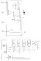
- FIG. 1Billustrates one example of a typical bi-directional output buffer 100 .
- buffer 100is coupled to memory modules 194 A- 194 B via bus 197 .
- Buffer 100is configured to receive output enable 102 , data out 104 , and data in 106 . Included in buffer 100 are nand gate 130 , inverter 132 , and nor gate 134 .
- transistor 120is turned on when both the output enable 102 and data out 104 are asserted, and the output signal 124 is driven via I/O pad 160 . If both the output enable 102 and data out 104 are low, then transistor 122 is turned on and a corresponding signal 124 driven out via I/O pad 160 .
- Bus 197includes termination resistors 191 and 192 .
- Buffer 100is configured to both drive and receive signals.
- buffer 100may both write to, and receive data from, memory modules 194 .
- output enable 102will be negated when receiving data via I/O pad 160 .
- both transistors 120 and 122are turned off.
- Each of memory modules 194include a particular output impedance.
- the output impedance of buffer 100may not be equal to that of memory modules 194 . Consequently, utilizing series resistor 191 to create an output impedance for buffer 100 which matches the characteristic impedance of bus 197 may be appropriate for when buffer 100 is driving, but may not be an appropriate value for when modules 194 are driving and buffer 100 is receiving.
- a bi-directional output bufferwhich includes active termination.
- the bufferhas at least two operating modes, including a driving mode and a receiving mode.
- a high impedance modemay also be included.
- the bufferWhen operating in driving mode, the buffer is configured to have an output impedance of a specified strength.
- the bufferWhen operating in a receiving mode, is configured to another specified impedance as an active termination.
- the buffermay also be configured such that resistive components are shared between the driving and receiving modes.
- FIG. 1Aillustrates a prior art output buffer
- FIG. 1Billustrates a prior art bi-directional output buffer.
- FIG. 2is a block diagram of one embodiment of a bi-directional buffer.
- FIG. 3is a diagram of one embodiment of a bi-directional buffer.
- FIG. 4is a table describing one embodiment of the operation of the buffer in FIG. 3 .
- FIG. 5is a block diagram of one embodiment of a bi-directional buffer.
- FIG. 6is a diagram of one embodiment of a bi-directional buffer.
- FIG. 7is a table describing one embodiment of the operation of the buffer in FIG. 3 .
- FIG. 8illustrates on embodiment of a system including a bi-directional buffer.
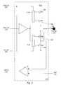
- Buffer 200includes a driver 210 and receiver 212 .
- Buffer 200is configured to receive Term_En signal 220 , Drv_En signal 224 , and Data Out signal 226 .
- Driver 210includes resistive elements 202 and 204 .
- Element 202is coupled to VCC and element 204 is coupled to ground.
- switch 208is also included in driver 210 which is configured to alternately couple element 202 or element 204 to output signal 230 .
- Buffer 200is also configured to receive signals via I/O pad 240 which are conveyed to comparator 212 .
- Comparator 212is also coupled to Term_En signal 220 .
- buffer 200is configured to operate in at least two modes—driving and receiving.
- buffer 200may be configured to operate in a third, high impedance, mode.
- Term_En signal 220is configured to operate as a termination enable signal. When active, Term_En configures buffer 200 to provide termination in receiving mode.
- Drv_En 224is configured to act as a driver enable signal.
- Data Out 226provides data to buffer 220 which is to be driven.
- Term_En 220is also coupled to comparator 212 via inverted enable input. Consequently, when Term_En 220 is active, driver 210 is configured to provide receive termination and comparator 212 is configured to receive data via I/O pad 240 , which is then conveyed as Data In 228 .
- buffer 200is configured to provide active termination when in receiving mode.
- the active termination impedance provided by buffer 200may be different than the output impedance of buffer 200 .
- buffer 200is configured to reduce the number of components required by sharing components between both driving and receiving modes.
- FIG. 3illustrates one embodiment of buffer 200 .
- buffer 200includes p-channel transistors Ru 1 302 and Ru 2 306 , and n-channel transistors Rd 1 304 and Rd 2 308 .
- circuitry 310 Awhich is coupled to Term_En 220 , Data Out 226 , Ru 1 302 gate, and Rd 1 304 gate.
- Circuit 310 Bis coupled to Data Out 226 , Drv_En 224 , Ru 2 306 gate, and Rd 2 308 gate.
- Circuits 310are configured to apply selected values to the gates of transistors 302 - 308 in order to either turn on or off each transistor.
- Term-En 220is also coupled to receive circuitry 229 via inverted input.
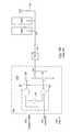
- Table 400which describes the operation of the embodiment of buffer 200 shown in FIG. 3 .
- Table 400includes nine columns and six rows.
- Column 401indicates a mode of operation of buffer 200 , which each of the remaining columns of table 400 indicate the value of a particular signal or component of buffer 200 .
- Four modes of operationare described by each of rows 402 - 408 .
- a mode of operation wherein Term_En 220 is asserted and Drv_En 224 is also assertedis not permitted, or undefined.
- a first mode of operation, Hi Z,is described in row 402 .
- circuits 310are configured to turn off all transistors 302 - 310 , and place output signal 230 in a high impedance state.
- buffer 200is configured to drive, or transmit (TX), a logic high signal.
- TXtransmit
- buffer 200is configured to drive the value of Data Out 226 as output signal 230 .
- circuits 310are configured to turn off transistors Ru 1 302 and Ru 2 306 , and turn on transistors Rd 1 304 and Rd 2 308 .
- circuits 310are configured to turn on transistors Ru 1 302 and Ru 2 306 , while turning off transistors Rd 1 304 and Rd 2 308 .
- buffer 200is configured to operate in receiving (RX) mode 408 .
- circuits 310are configured to turn on transistors Ru 1 302 and Rd 1 306 , while turning off transistors Ru 2 306 and Rd 2 308 .
- transistors Ru 1 302 and Rd 1 304are weaker than transistors Ru 2 306 and Rd 2 308 , respectively.
- buffer 200when buffer 200 is driving both a strong transistor and a weak transistor will be on. This combination of strong and weak transistor has a particular driving impedance.
- weaker transistors Ru 1 302 and Rd 1 304when buffer 200 is in receiving mode, weaker transistors Ru 1 302 and Rd 1 304 are turned on and provide an active receiving termination.
- transistors Ru 1 302 and Rd 1 304are weak relative to those transistors which are on when driving. Consequently, the active termination provided by transistors Ru 1 302 and Rd 1 304 may have a lower impedance than the driving impedance. In this manner, improved impedance matching may be obtained for both driving and receiving modes in a single buffer. Further, by sharing resistive elements, transistors in this case, between driving and receiving modes, fewer elements may be required in the construction of buffer 200 .
- FIG. 5a block diagram of an alternative embodiment of a bi-directional buffer 590 is shown.
- the buffer 590 of FIG. 5is similar to the buffer 200 of FIG. 2, with the exception of particular signals input to buffer 590 .
- buffer 590does not include the Term_En signal 220 and Drv_En signal 224 of buffer 200 . Rather, buffer 590 includes a Hi-z signal 560 and Enable signal 562 .
- FIG. 6illustrates one embodiment of buffer 590 .
- Enable signal 562is coupled to circuitry 610 and receive circuitry 229 .
- Hi-z signal 560is coupled to circuitry 610 .
- Operation of buffer 590is illustrated by table 700 of FIG. 7 . Rows 702 - 708 describe various modes of operation of buffer 590 .
- Hi_z signal 562is asserted, transistors 302 , 304 , 306 , and 308 are turned off, and output 230 is placed in a Hi-z state.
- buffer 590In a second mode 704 of operation, buffer 590 is configured to transmit a logic low signal (Data Out 226 is low).
- Enable signal 560is asserted, Hi-z 562 is negated, transistors 302 and 306 are off, and transistors 304 and 308 are turned on.
- a logic low signalis then driven on Output 230 .
- Enable 560is asserted, Hi_z 562 is negated, transistors 302 and 306 are turned on, and transistors 304 and 308 are turned off.
- both Enable 560 and Hi_z 562are negated, transistors 302 and 304 are turned on, and transistors 306 and 308 are turned off.
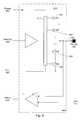
- FIG. 8illustrates one embodiment of a system 500 incorporating a bi-directional buffer as described above.
- FIG. 8includes a memory controller 502 coupled to memory modules 194 A- 194 D and clock source 520 .
- Controller 502is coupled to memory modules 194 A and 194 B via command/address bus 510 A.
- Controller 502is coupled to memory modules 194 C and 194 D via command/address bus 510 B.
- controller 502includes bi-directional buffer 550 which is coupled to each of memory modules 194 via data bus 530 .
- buses 510 and 530are terminated 560 with resistors RT.
- clock source 520is also coupled to each of memory modules 194 .
- system 500is a synchronous DRAM (SDRAM) system.
- SDRAMsynchronous DRAM
- buffer 550is configured to both drive and receive data via data bus 530 .
- buffer 550sees a particular load impedance and may be configured to provide a matching impedance to improve signal integrity.
- the impedance with which buffer 550 is configured for drivingmay not be appropriate for receiving. Consequently, buffer 550 is configured to provide active termination with a different impedance than the driving impedance. Because buffer 550 is configured to provide active termination, no series resistor is needed on bus 530 .
- buffer 550may be configured to share components in providing both the driving and receiving impedances which may reduce the size and/or component count of buffer 550 .
Landscapes
- Engineering & Computer Science (AREA)
- Signal Processing (AREA)
- General Engineering & Computer Science (AREA)
- Theoretical Computer Science (AREA)
- Computer Networks & Wireless Communication (AREA)
- Physics & Mathematics (AREA)
- Computer Hardware Design (AREA)
- General Physics & Mathematics (AREA)
- Power Engineering (AREA)
- Logic Circuits (AREA)
- Dram (AREA)
- Memory System (AREA)
- Networks Using Active Elements (AREA)
Abstract
Description
1. Field of the Invention
This invention relates to digital communication systems, and more particularly to I/O devices.
2. Description of the Relevant Art
One issue that is typically considered when designing electrical communication systems is that of ringing, or reflections, on transmission lines. Various termination techniques are often utilized in order to reduce the ringing, and the resultant signal distortion, that may occur on a transmission line. For example, one or more electrically resistive elements (e.g., resistors) may be inserted between a driver and an end of a transmission line in order to cause the effective output impedance of the driver to more closely match the characteristic impedance of the transmission line. Similarly, one or more electrically resistive elements may be coupled to an end of a transmission line at a receiver in order to cause the effective input impedance of the receiver to more closely match the characteristic impedance of the transmission line.
FIG. 1A illustrates one example of a driver and receiver which utilize termination. In the example shown, an output buffer (driver) includestransistors output signal 124. A receiver includes acomparator 190 coupled to receive aninput voltage 186 and reference voltage Vref. Aseries resistor 186 has been added to thetransmission line 183 in order to reduce signal reflections and distortion within the transmission line.Series resistor 186 may, for example, have a value equal to the characteristic impedance of the transmission line. Asecond termination resistor 184, also having a value equal to the characteristic impedance oftransmission line 183, is connected between the first input terminal ofop amp 190 and power supply voltage level VTT.
While both ends termination as illustrated in FIG. 1A reduces signal reflections, it also results in half amplitude received signals. Whenfirst termination resistor 186 andsecond termination resistor 184 are coupled to opposite ends oftransmission line 183 in order to reduce signal reflections and distortion, they form a voltage divider network which restricts the range of voltage levels which may be used to convey signals from the driver to the receiver. Consequently, a more sensitive receiver is required.
FIG. 1B illustrates one example of a typicalbi-directional output buffer 100. In the example shown,buffer 100 is coupled tomemory modules 194A-194B viabus 197.Buffer 100 is configured to receive output enable102, data out104, and data in106. Included inbuffer 100 arenand gate 130,inverter 132, and norgate 134. As is apparent from the figure,transistor 120 is turned on when both the output enable102 and data out104 are asserted, and theoutput signal 124 is driven via I/O pad 160. If both the output enable102 and data out104 are low, thentransistor 122 is turned on and acorresponding signal 124 driven out via I/O pad 160.Bus 197 includestermination resistors
What is desired is a bi-directional buffer with improved performance characteristics.
A bi-directional output buffer is contemplated which includes active termination. The buffer has at least two operating modes, including a driving mode and a receiving mode. A high impedance mode may also be included. When operating in driving mode, the buffer is configured to have an output impedance of a specified strength. When operating in a receiving mode, the buffer is configured to another specified impedance as an active termination. In addition to providing for differing driving and receiving impedances, the buffer may also be configured such that resistive components are shared between the driving and receiving modes.
Other objects and advantages of the invention will become apparent upon reading the following detailed description and upon reference to the accompanying drawings in which:
FIG. 1A illustrates a prior art output buffer.
FIG. 1B illustrates a prior art bi-directional output buffer.
FIG. 2 is a block diagram of one embodiment of a bi-directional buffer.
FIG. 3 is a diagram of one embodiment of a bi-directional buffer.
FIG. 4 is a table describing one embodiment of the operation of the buffer in FIG.3.
FIG. 5 is a block diagram of one embodiment of a bi-directional buffer.
FIG. 6 is a diagram of one embodiment of a bi-directional buffer.
FIG. 7 is a table describing one embodiment of the operation of the buffer in FIG.3.
FIG. 8 illustrates on embodiment of a system including a bi-directional buffer.
While the invention is susceptible to various modifications and alternative forms, specific embodiments thereof are shown by way of example in the drawings and will herein be described in detail. It should be understood, however, that the drawings and detailed description thereto are not intended to limit the invention to the particular form disclosed, but on the contrary, the intention is to cover all modifications, equivalents and alternatives falling within the spirit and scope of the present invention as defined by the appended claims.
Turning now to FIG. 2, a block diagram of one embodiment of abi-directional buffer 200 is shown.Buffer 200 includes adriver 210 andreceiver 212.Buffer 200 is configured to receiveTerm_En signal 220,Drv_En signal 224, andData Out signal 226.Driver 210 includesresistive elements Element 202 is coupled to VCC andelement 204 is coupled to ground. Also included indriver 210 isswitch 208 which is configured to alternatelycouple element 202 orelement 204 tooutput signal 230.Buffer 200 is also configured to receive signals via I/O pad 240 which are conveyed tocomparator 212.Comparator 212 is also coupled to Term_En signal220.
Generally speaking, in the embodiment shown,buffer 200 is configured to operate in at least two modes—driving and receiving. In addition,buffer 200 may be configured to operate in a third, high impedance, mode.Term_En signal 220 is configured to operate as a termination enable signal. When active, Term_En configuresbuffer 200 to provide termination in receiving mode.Drv_En 224 is configured to act as a driver enable signal.Data Out 226 provides data to buffer220 which is to be driven. As can be seen from the example of FIG. 2,Term_En 220 is also coupled tocomparator 212 via inverted enable input. Consequently, whenTerm_En 220 is active,driver 210 is configured to provide receive termination andcomparator 212 is configured to receive data via I/O pad 240, which is then conveyed as Data In228.
As mentioned above,buffer 200 is configured to provide active termination when in receiving mode. The active termination impedance provided bybuffer 200 may be different than the output impedance ofbuffer 200. Still further, as will be discussed below,buffer 200 is configured to reduce the number of components required by sharing components between both driving and receiving modes.
FIG. 3 illustrates one embodiment ofbuffer 200. In the embodiment of FIG. 3,buffer 200 includes p-channel transistors Ru1 302 andRu2 306, and n-channel transistors Rd1304 andRd2 308. Also included iscircuitry 310A which is coupled toTerm_En 220,Data Out 226,Ru1 302 gate, andRd1 304 gate.Circuit 310B is coupled toData Out 226,Drv_En 224,Ru2 306 gate, andRd2 308 gate. Circuits310 are configured to apply selected values to the gates of transistors302-308 in order to either turn on or off each transistor. Term-En 220 is also coupled to receive circuitry229 via inverted input.
Referring to FIG. 4, a table400 is shown which describes the operation of the embodiment ofbuffer 200 shown in FIG.3. Table400 includes nine columns and six rows.Column 401 indicates a mode of operation ofbuffer 200, which each of the remaining columns of table400 indicate the value of a particular signal or component ofbuffer 200. Four modes of operation are described by each of rows402-408. In one embodiment, a mode of operation whereinTerm_En 220 is asserted andDrv_En 224 is also asserted is not permitted, or undefined.
A first mode of operation, Hi Z, is described inrow 402. WhenTerm_En 220 andDrv_En 224 are both negated, circuits310 are configured to turn off all transistors302-310, andplace output signal 230 in a high impedance state. In a second mode of operation,buffer 200 is configured to drive, or transmit (TX), a logic high signal. In response to detectingTerm_En 220 is low andDrv_En 224 is high,buffer 200 is configured to drive the value ofData Out 226 asoutput signal 230. When driving andData Out 226 is low, a binary “0” in this example, circuits310 are configured to turn offtransistors Ru1 302 andRu2 306, and turn on transistors Rd1304 andRd2 308. On the other hand, when driving andData Out 226 is high, circuits310 are configured to turn ontransistors Ru1 302 andRu2 306, while turning off transistors Rd1304 andRd2 308. Finally, whenTerm_En 220 is asserted andDrv_En 224 is negated,buffer 200 is configured to operate in receiving (RX)mode 408. When in receivingmode 408, circuits310 are configured to turn ontransistors Ru1 302 andRd1 306, while turning offtransistors Ru2 306 andRd2 308.
In one embodiment,transistors Ru1 302 andRd1 304 are weaker than transistors Ru2306 andRd2 308, respectively. As described above, whenbuffer 200 is driving both a strong transistor and a weak transistor will be on. This combination of strong and weak transistor has a particular driving impedance. In contrast, whenbuffer 200 is in receiving mode, weaker transistors Ru1302 andRd1 304 are turned on and provide an active receiving termination. In addition,transistors Ru1 302 andRd1 304 are weak relative to those transistors which are on when driving. Consequently, the active termination provided by transistors Ru1302 andRd1 304 may have a lower impedance than the driving impedance. In this manner, improved impedance matching may be obtained for both driving and receiving modes in a single buffer. Further, by sharing resistive elements, transistors in this case, between driving and receiving modes, fewer elements may be required in the construction ofbuffer 200.
Turning now to FIG. 5, a block diagram of an alternative embodiment of abi-directional buffer 590 is shown. Thebuffer 590 of FIG. 5 is similar to thebuffer 200 of FIG. 2, with the exception of particular signals input to buffer590. For example,buffer 590 does not include theTerm_En signal 220 and Drv_En signal224 ofbuffer 200. Rather, buffer590 includes a Hi-z signal 560 and Enable signal562.
FIG. 6 illustrates one embodiment ofbuffer 590. Enablesignal 562 is coupled tocircuitry 610 and receive circuitry229. Hi-z signal 560 is coupled tocircuitry 610. Operation ofbuffer 590 is illustrated by table700 of FIG.7. Rows702-708 describe various modes of operation ofbuffer 590. In afirst mode 702 of operation,Hi_z signal 562 is asserted,transistors output 230 is placed in a Hi-z state. In asecond mode 704 of operation,buffer 590 is configured to transmit a logic low signal (Data Out 226 is low). In this mode of operation, Enable signal560 is asserted, Hi-z 562 is negated,transistors transistors Output 230. When driving a logic high signal (Data Out 226 is high),Enable 560 is asserted,Hi_z 562 is negated,transistors transistors termination mode 708, bothEnable 560 andHi_z 562 are negated,transistors transistors
FIG. 8 illustrates one embodiment of a system500 incorporating a bi-directional buffer as described above. FIG. 8 includes amemory controller 502 coupled tomemory modules 194A-194D andclock source 520.Controller 502 is coupled tomemory modules address bus 510A.Controller 502 is coupled tomemory modules address bus 510B. In addition,controller 502 includesbi-directional buffer 550 which is coupled to each of memory modules194 viadata bus 530. Each ofbuses 510 and530 are terminated560 with resistors RT. Finally,clock source 520 is also coupled to each of memory modules194.
In one embodiment, system500 is a synchronous DRAM (SDRAM) system. However, numerous other possible memory configurations and applications are possible and are contemplated. In a manner as described above,buffer 550 is configured to both drive and receive data viadata bus 530. When driving,buffer 550 sees a particular load impedance and may be configured to provide a matching impedance to improve signal integrity. However, as already noted, when receiving, the impedance with whichbuffer 550 is configured for driving may not be appropriate for receiving. Consequently,buffer 550 is configured to provide active termination with a different impedance than the driving impedance. Becausebuffer 550 is configured to provide active termination, no series resistor is needed onbus 530. By eliminating the need for the series resistor, passive components (such as series resistors) on the printed circuit board (PCB) may be reduced and more routing channels between thecontroller 502 and the memory modules194 may be realized. Still further, buffer550 may be configured to share components in providing both the driving and receiving impedances which may reduce the size and/or component count ofbuffer 550.
While the present invention has been described with reference to particular embodiments, it will be understood that the embodiments are illustrative and that the invention scope is not limited to these embodiments. For example, while CMOS components are used in the above illustrations, other components and switching mechanisms may be utilized as well. In addition, it will be recognized that alternative embodiments may utilize alternate logic states to assert or negate signals. Many variations, modifications, additions and improvements to the embodiments described are possible. These variations, modifications, additions and improvements may fall within the scope of the invention as detailed within the following claims.
Claims (17)
1. A bi-directional buffer comprising:
a driver component;
a receiver component; and
circuitry configured to:
select a driving mode of operation in response to detecting a first condition, wherein said driving mode comprises a first impedance; and
select a receiving mode of operation in response to detecting a second condition, wherein said receiving mode provides active termination;
wherein said active termination comprises a second impedance which is different than said first impedance.
2. The buffer ofclaim 1 , wherein said driver component comprises four transistors including a first transistor, a second transistor, a third transistor, and a fourth transistor, and wherein said active termination comprises at least two of said transistors.
3. The buffer ofclaim 2 , wherein said circuitry is configured to turn on said first and third transistors, and turn off said second and fourth transistors, in response to detecting said driving mode and detecting a data with a high logic value is being driven.
4. The buffer ofclaim 2 , wherein said circuitry is configured to turn on said second and fourth transistors, and turn off said first and third transistors, in response to detecting said driving mode and detecting a data with a low logic value is being driven.
5. The buffer ofclaim 2 , wherein said circuitry is configured to turn on said first and second transistors, and turn off said third and fourth transistors, in response to detecting said receiving mode.
6. The buffer ofclaim 1 , wherein detecting said first condition comprises detecting the assertion of a drive enable signal, and wherein detecting said second condition comprises detecting the assertion of a termination enable signal.
7. The buffer ofclaim 1 , wherein said circuitry is further configured to provide a high impedance mode of operation.
8. A system comprising:
a data bus;
a storage device coupled to said data bus; and
a memory controller including a buffer coupled to said data bus, wherein said buffer is configured to:
drive data onto said data bus in response to detecting a first mode of operation, wherein said first mode comprises a first impedance; and
receive data via said data bus in response to detecting a second mode of operation, wherein said second mode provides active termination with a second impedance which is different than said first impedance.
9. The system ofclaim 8 , wherein said buffer comprises four transistors including a first transistor, a second transistor, a third transistor, and a fourth transistor, and wherein said active termination comprises at least two of said transistors.
10. The system ofclaim 9 , wherein said buffer is configured to turn on said first and third transistors, and turn off said second and fourth transistors, in response to detecting said first mode of operation and detecting a data with a high logic value is being driven.
11. The system ofclaim 10 , wherein said buffer is configured to turn on said second and fourth transistors, and turn off said first and third transistors, in response to detecting said first mode of operation and detecting a data with a low logic value is being driven.
12. The system ofclaim 11 , wherein said buffer is configured to turn on said first and second transistors, and turn off said third and fourth transistors, in response to detecting said receiving mode.
13. The system ofclaim 8 , wherein detecting said first mode of operation comprises detecting the assertion of a drive enable signal, and wherein detecting said second mode of operation comprises detecting the assertion of a termination enable signal.
14. The system ofclaim 8 , wherein said buffer is further configured to provide a high impedance mode of operation.
15. The system ofclaim 8 , wherein said data bus comprises an impedance substantially equivalent to said first impedance.
16. A method of bi-directional communication comprising:
selecting a driving mode of operation in response to detecting a first condition, wherein said driving mode comprises a first impedance;
selecting a receiving mode of operation in response to detecting a second condition, wherein said receiving mode comprises an active termination with a second impedance which is different than said first impedance.
17. The method ofclaim 16 , wherein said first and second impedance comprise shared components.
Priority Applications (3)
| Application Number | Priority Date | Filing Date | Title |
|---|---|---|---|
| US10/027,544US6690191B2 (en) | 2001-12-21 | 2001-12-21 | Bi-directional output buffer |
| EP02258756AEP1324554A3 (en) | 2001-12-21 | 2002-12-19 | Bi-directional buffer with impedance matching |
| JP2002372994AJP4505653B2 (en) | 2001-12-21 | 2002-12-24 | Bidirectional output buffer |
Applications Claiming Priority (1)
| Application Number | Priority Date | Filing Date | Title |
|---|---|---|---|
| US10/027,544US6690191B2 (en) | 2001-12-21 | 2001-12-21 | Bi-directional output buffer |
Publications (2)
| Publication Number | Publication Date |
|---|---|
| US20030117172A1 US20030117172A1 (en) | 2003-06-26 |
| US6690191B2true US6690191B2 (en) | 2004-02-10 |
Family
ID=21838331
Family Applications (1)
| Application Number | Title | Priority Date | Filing Date |
|---|---|---|---|
| US10/027,544Expired - LifetimeUS6690191B2 (en) | 2001-12-21 | 2001-12-21 | Bi-directional output buffer |
Country Status (3)
| Country | Link |
|---|---|
| US (1) | US6690191B2 (en) |
| EP (1) | EP1324554A3 (en) |
| JP (1) | JP4505653B2 (en) |
Cited By (64)
| Publication number | Priority date | Publication date | Assignee | Title |
|---|---|---|---|---|
| US20030023788A1 (en)* | 2001-07-24 | 2003-01-30 | International Business Machines Corporation | Data input/output device, memory system, data input/output circuit, and data input/output method |
| US20030234664A1 (en)* | 2002-06-20 | 2003-12-25 | Mitsubishi Denki Kabushiki Kaisha | Data bus |
| US20040019758A1 (en)* | 2002-07-29 | 2004-01-29 | Elpida Memory, Inc. | Memory module and memory system suitable for high speed operation |
| US20040036498A1 (en)* | 2002-08-23 | 2004-02-26 | Park Youn-Sik | Semiconductor integrated circuit having on-chip termination |
| US20040114412A1 (en)* | 2002-12-12 | 2004-06-17 | International Business Machines Corporation | Method and system for intelligent bi-direction signal net with dynamically configurable input/output cell |
| US20040135646A1 (en)* | 2002-08-01 | 2004-07-15 | Bernhard Rall | Circuit for adapting characteristic wave impedance |
| US20040145393A1 (en)* | 2002-07-29 | 2004-07-29 | Samsung Electronics Co., Ltd. | Integrated circuit with on-chip termination |
| US20040186956A1 (en)* | 2000-01-05 | 2004-09-23 | Richard Perego | Configurable width buffered module |
| US20040201401A1 (en)* | 2003-04-09 | 2004-10-14 | Agere Systems, Inc. | Bi-directional impedance matching circuit |
| US20040223365A1 (en)* | 2003-05-07 | 2004-11-11 | Choi Jung-Hwan | Semiconductor device and method for inputting/outputting data simultaneously through single pad |
| US20040256638A1 (en)* | 2000-01-05 | 2004-12-23 | Richard Perego | Configurable width buffered module having a bypass circuit |
| US6842038B1 (en)* | 2003-09-25 | 2005-01-11 | International Business Machines Corporation | Self optimizing off chip driver |
| US20050007805A1 (en)* | 2000-01-05 | 2005-01-13 | Fred Ware | Configurable width buffered module having flyby elements |
| US20050010737A1 (en)* | 2000-01-05 | 2005-01-13 | Fred Ware | Configurable width buffered module having splitter elements |
| US20050151563A1 (en)* | 2002-08-23 | 2005-07-14 | Park Youn-Sik | Semiconductor integrated circuit having on-chip termination |
| US20050166026A1 (en)* | 2000-01-05 | 2005-07-28 | Fred Ware | Configurable width buffered module having switch elements |
| US20060022702A1 (en)* | 2004-07-30 | 2006-02-02 | Fujitsu Limited | Interface circuit and constituting method thereof |
| US20060170450A1 (en)* | 2005-01-31 | 2006-08-03 | Pelley Perry H | Integrated circuit with programmable-impedance output buffer and method therefor |
| US20060214681A1 (en)* | 2005-01-07 | 2006-09-28 | Shoji Kojima | Impedance matching circuit, input-output circuit and semiconductor test apparatus |
| US20070058471A1 (en)* | 2005-09-02 | 2007-03-15 | Rajan Suresh N | Methods and apparatus of stacking DRAMs |
| US20070070669A1 (en)* | 2005-09-26 | 2007-03-29 | Rambus Inc. | Memory module including a plurality of integrated circuit memory devices and a plurality of buffer devices in a matrix topology |
| US20070085576A1 (en)* | 2005-10-14 | 2007-04-19 | Hector Sanchez | Output driver circuit with multiple gate devices |
| US20070192563A1 (en)* | 2006-02-09 | 2007-08-16 | Rajan Suresh N | System and method for translating an address associated with a command communicated between a system and memory circuits |
| US20070204075A1 (en)* | 2006-02-09 | 2007-08-30 | Rajan Suresh N | System and method for reducing command scheduling constraints of memory circuits |
| US20070216445A1 (en)* | 2006-03-14 | 2007-09-20 | Inphi Corporation | Output buffer with switchable output impedance |
| US20080027697A1 (en)* | 2006-07-31 | 2008-01-31 | Metaram, Inc. | Memory circuit simulation system and method with power saving capabilities |
| US20080028136A1 (en)* | 2006-07-31 | 2008-01-31 | Schakel Keith R | Method and apparatus for refresh management of memory modules |
| US20080025136A1 (en)* | 2006-07-31 | 2008-01-31 | Metaram, Inc. | System and method for storing at least a portion of information received in association with a first operation for use in performing a second operation |
| US20080025122A1 (en)* | 2006-07-31 | 2008-01-31 | Metaram, Inc. | Memory refresh system and method |
| US20080031166A1 (en)* | 2006-08-03 | 2008-02-07 | Fujitsu Limited | Bidirectional transmission circuit and sending/receiving element |
| US20080079457A1 (en)* | 2006-09-29 | 2008-04-03 | Mediatek Inc. | High speed IO buffer |
| US20080080261A1 (en)* | 2005-09-26 | 2008-04-03 | Rambus Inc. | Memory system topologies including a buffer device and an integrated circuit memory device |
| US20080106836A1 (en)* | 2002-05-14 | 2008-05-08 | Darrin Benzer | Io clamping circuit method utilizing output driver transistors |
| US20080115006A1 (en)* | 2006-07-31 | 2008-05-15 | Michael John Sebastian Smith | System and method for adjusting the timing of signals associated with a memory system |
| US20080126690A1 (en)* | 2006-02-09 | 2008-05-29 | Rajan Suresh N | Memory module with memory stack |
| US20080133825A1 (en)* | 2006-07-31 | 2008-06-05 | Suresh Natarajan Rajan | System and method for simulating an aspect of a memory circuit |
| US20080191734A1 (en)* | 2007-02-09 | 2008-08-14 | Samsung Electronics Co., Ltd. | Semiconductor device including on-die termination control circuit having pipe line varying with frequency range |
| US20080284466A1 (en)* | 2007-05-18 | 2008-11-20 | Cranford Jr Hayden Clavie | Driver Circuit |
| US20090024790A1 (en)* | 2006-07-31 | 2009-01-22 | Suresh Natarajan Rajan | Memory circuit system and method |
| US20090174437A1 (en)* | 2008-01-08 | 2009-07-09 | Fujitsu Microelectronics Limited | Semiconductor Device and Method for Controlling Thereof |
| US20090216939A1 (en)* | 2008-02-21 | 2009-08-27 | Smith Michael J S | Emulation of abstracted DIMMs using abstracted DRAMs |
| US20090319719A1 (en)* | 2000-01-05 | 2009-12-24 | Rambus Inc. | System Having A Controller Device, A Buffer Device And A Plurality Of Memory Devices |
| US20100257304A1 (en)* | 2006-07-31 | 2010-10-07 | Google Inc. | Apparatus and method for power management of memory circuits by a system or component thereof |
| US20100281280A1 (en)* | 2006-07-31 | 2010-11-04 | Google Inc. | Interface Circuit System And Method For Performing Power Management Operations In Conjunction With Only A Portion Of A Memory Circuit |
| US20110095783A1 (en)* | 2009-06-09 | 2011-04-28 | Google Inc. | Programming of dimm termination resistance values |
| US8080874B1 (en) | 2007-09-14 | 2011-12-20 | Google Inc. | Providing additional space between an integrated circuit and a circuit board for positioning a component therebetween |
| US8111566B1 (en) | 2007-11-16 | 2012-02-07 | Google, Inc. | Optimal channel design for memory devices for providing a high-speed memory interface |
| US8130560B1 (en) | 2006-11-13 | 2012-03-06 | Google Inc. | Multi-rank partial width memory modules |
| US8335894B1 (en) | 2008-07-25 | 2012-12-18 | Google Inc. | Configurable memory system with interface circuit |
| US8370566B2 (en) | 2006-10-05 | 2013-02-05 | Google Inc. | System and method for increasing capacity, performance, and flexibility of flash storage |
| US8386722B1 (en) | 2008-06-23 | 2013-02-26 | Google Inc. | Stacked DIMM memory interface |
| US8386833B2 (en) | 2005-06-24 | 2013-02-26 | Google Inc. | Memory systems and memory modules |
| US8397013B1 (en) | 2006-10-05 | 2013-03-12 | Google Inc. | Hybrid memory module |
| US8566556B2 (en) | 2006-02-09 | 2013-10-22 | Google Inc. | Memory module with memory stack and interface with enhanced capabilities |
| US8588017B2 (en) | 2010-10-20 | 2013-11-19 | Samsung Electronics Co., Ltd. | Memory circuits, systems, and modules for performing DRAM refresh operations and methods of operating the same |
| US8595419B2 (en) | 2006-07-31 | 2013-11-26 | Google Inc. | Memory apparatus operable to perform a power-saving operation |
| US8705240B1 (en) | 2007-12-18 | 2014-04-22 | Google Inc. | Embossed heat spreader |
| US8796830B1 (en) | 2006-09-01 | 2014-08-05 | Google Inc. | Stackable low-profile lead frame package |
| US8949519B2 (en) | 2005-06-24 | 2015-02-03 | Google Inc. | Simulating a memory circuit |
| US9171585B2 (en) | 2005-06-24 | 2015-10-27 | Google Inc. | Configurable memory circuit system and method |
| US9507739B2 (en) | 2005-06-24 | 2016-11-29 | Google Inc. | Configurable memory circuit system and method |
| US10013371B2 (en) | 2005-06-24 | 2018-07-03 | Google Llc | Configurable memory circuit system and method |
| US10498385B2 (en) | 2017-05-24 | 2019-12-03 | SK Hynix Inc. | Tranceiver circuit and receiver circuit |
| US11328764B2 (en) | 2005-09-26 | 2022-05-10 | Rambus Inc. | Memory system topologies including a memory die stack |
Families Citing this family (14)
| Publication number | Priority date | Publication date | Assignee | Title |
|---|---|---|---|---|
| US7110400B2 (en) | 2002-04-10 | 2006-09-19 | Integrated Device Technology, Inc. | Random access memory architecture and serial interface with continuous packet handling capability |
| KR100583636B1 (en)* | 2003-08-19 | 2006-05-26 | 삼성전자주식회사 | Device for controlling impedance of termination circuit and off-chip drive circuit using single reference resistor |
| TWI355792B (en)* | 2003-08-29 | 2012-01-01 | Rohm Co Ltd | Power supply and electronic device having same |
| CN103116565A (en)* | 2005-04-21 | 2013-05-22 | 提琴存储器公司 | Configurable switching element, interconnection network and interconnection method among networks |
| US8112655B2 (en)* | 2005-04-21 | 2012-02-07 | Violin Memory, Inc. | Mesosynchronous data bus apparatus and method of data transmission |
| US9286198B2 (en) | 2005-04-21 | 2016-03-15 | Violin Memory | Method and system for storage of data in non-volatile media |
| US8452929B2 (en)* | 2005-04-21 | 2013-05-28 | Violin Memory Inc. | Method and system for storage of data in non-volatile media |
| US9582449B2 (en) | 2005-04-21 | 2017-02-28 | Violin Memory, Inc. | Interconnection system |
| US9384818B2 (en) | 2005-04-21 | 2016-07-05 | Violin Memory | Memory power management |
| US8028186B2 (en) | 2006-10-23 | 2011-09-27 | Violin Memory, Inc. | Skew management in an interconnection system |
| JP5157661B2 (en)* | 2008-06-12 | 2013-03-06 | 富士通セミコンダクター株式会社 | Termination resistance adjustment circuit and bus system |
| KR20110027387A (en)* | 2009-09-10 | 2011-03-16 | 삼성전자주식회사 | A transmission / reception system, a semiconductor device of the system, and a data transmission / reception method of the system |
| US9698778B2 (en)* | 2014-09-30 | 2017-07-04 | Taiwan Semiconductor Manufacturing Company, Ltd. | On-die termination/driving circuit and method of using the same |
| CN117220650A (en)* | 2023-11-07 | 2023-12-12 | 合肥奎芯集成电路设计有限公司 | Pre-punching processing circuit with de-emphasis function |
Citations (7)
| Publication number | Priority date | Publication date | Assignee | Title |
|---|---|---|---|---|
| US5371424A (en)* | 1992-11-25 | 1994-12-06 | Motorola, Inc. | Transmitter/receiver circuit and method therefor |
| US5498990A (en)* | 1991-11-05 | 1996-03-12 | Monolithic System Technology, Inc. | Reduced CMOS-swing clamping circuit for bus lines |
| US5532621A (en) | 1993-12-24 | 1996-07-02 | Kawasaki Steel Corporation | Output buffer circuit, input buffer circuit and bi-directional buffer circuit for plural voltage systems |
| US5652528A (en)* | 1994-11-25 | 1997-07-29 | Hitachi, Ltd. | Transceiver circuit and method of transmitting a signal which uses an output transistor to send data and assist in pulling up a bus |
| US5929657A (en) | 1996-06-29 | 1999-07-27 | Hyundai Electronics Industries Co., | Circuit for controlling sense amplifiers |
| US6054881A (en)* | 1998-01-09 | 2000-04-25 | Advanced Micro Devices, Inc. | Input/output (I/O) buffer selectively providing resistive termination for a transmission line coupled thereto |
| US6127849A (en) | 1998-08-11 | 2000-10-03 | Texas Instruments Incorporated | Simultaneous bi-directional input/output (I/O) circuit |
Family Cites Families (4)
| Publication number | Priority date | Publication date | Assignee | Title |
|---|---|---|---|---|
| US5504782A (en)* | 1994-07-29 | 1996-04-02 | Motorola Inc. | Current mode transmitter and receiver for reduced RFI |
| US6051989A (en)* | 1997-05-30 | 2000-04-18 | Lucent Technologies Inc. | Active termination of a conductor for bi-directional signal transmission |
| FR2785409B1 (en)* | 1998-10-30 | 2001-09-21 | Bull Sa | TWO-WAY BIPINT CMOS LINK ADAPTED FOR RECEPTION AND TRANSMISSION |
| US6937111B2 (en)* | 2001-11-21 | 2005-08-30 | Hynix Semiconductor Inc. | Device and system having self-terminated driver and active terminator for high speed interface |
- 2001
- 2001-12-21USUS10/027,544patent/US6690191B2/ennot_activeExpired - Lifetime
- 2002
- 2002-12-19EPEP02258756Apatent/EP1324554A3/ennot_activeWithdrawn
- 2002-12-24JPJP2002372994Apatent/JP4505653B2/ennot_activeExpired - Lifetime
Patent Citations (7)
| Publication number | Priority date | Publication date | Assignee | Title |
|---|---|---|---|---|
| US5498990A (en)* | 1991-11-05 | 1996-03-12 | Monolithic System Technology, Inc. | Reduced CMOS-swing clamping circuit for bus lines |
| US5371424A (en)* | 1992-11-25 | 1994-12-06 | Motorola, Inc. | Transmitter/receiver circuit and method therefor |
| US5532621A (en) | 1993-12-24 | 1996-07-02 | Kawasaki Steel Corporation | Output buffer circuit, input buffer circuit and bi-directional buffer circuit for plural voltage systems |
| US5652528A (en)* | 1994-11-25 | 1997-07-29 | Hitachi, Ltd. | Transceiver circuit and method of transmitting a signal which uses an output transistor to send data and assist in pulling up a bus |
| US5929657A (en) | 1996-06-29 | 1999-07-27 | Hyundai Electronics Industries Co., | Circuit for controlling sense amplifiers |
| US6054881A (en)* | 1998-01-09 | 2000-04-25 | Advanced Micro Devices, Inc. | Input/output (I/O) buffer selectively providing resistive termination for a transmission line coupled thereto |
| US6127849A (en) | 1998-08-11 | 2000-10-03 | Texas Instruments Incorporated | Simultaneous bi-directional input/output (I/O) circuit |
Non-Patent Citations (2)
| Title |
|---|
| "EIA/JEDEC Standard", Stub Series Terminated Logic for 3.3 Volts (SSTL_3), EIA/JESD8-8; Electronic Industries Association, Engineering Department; Aug. 1996. |
| "SSTL for DIMM Applications"; Texas Instruments; Dec. 1997. |
Cited By (153)
| Publication number | Priority date | Publication date | Assignee | Title |
|---|---|---|---|---|
| US7356639B2 (en) | 2000-01-05 | 2008-04-08 | Rambus Inc. | Configurable width buffered module having a bypass circuit |
| US20040256638A1 (en)* | 2000-01-05 | 2004-12-23 | Richard Perego | Configurable width buffered module having a bypass circuit |
| US20050010737A1 (en)* | 2000-01-05 | 2005-01-13 | Fred Ware | Configurable width buffered module having splitter elements |
| US7404032B2 (en) | 2000-01-05 | 2008-07-22 | Rambus Inc. | Configurable width buffered module having switch elements |
| US20040186956A1 (en)* | 2000-01-05 | 2004-09-23 | Richard Perego | Configurable width buffered module |
| US7266634B2 (en) | 2000-01-05 | 2007-09-04 | Rambus Inc. | Configurable width buffered module having flyby elements |
| US20050166026A1 (en)* | 2000-01-05 | 2005-07-28 | Fred Ware | Configurable width buffered module having switch elements |
| US20050007805A1 (en)* | 2000-01-05 | 2005-01-13 | Fred Ware | Configurable width buffered module having flyby elements |
| US20090319719A1 (en)* | 2000-01-05 | 2009-12-24 | Rambus Inc. | System Having A Controller Device, A Buffer Device And A Plurality Of Memory Devices |
| US7526597B2 (en) | 2000-01-05 | 2009-04-28 | Rambus Inc. | Buffered memory having a control bus and dedicated data lines |
| US7363422B2 (en) | 2000-01-05 | 2008-04-22 | Rambus Inc. | Configurable width buffered module |
| US6961802B2 (en)* | 2001-07-24 | 2005-11-01 | International Business Machines Corporation | Data input/output device, memory system, data input/output circuit, and data input/output method |
| US20030023788A1 (en)* | 2001-07-24 | 2003-01-30 | International Business Machines Corporation | Data input/output device, memory system, data input/output circuit, and data input/output method |
| US20080106836A1 (en)* | 2002-05-14 | 2008-05-08 | Darrin Benzer | Io clamping circuit method utilizing output driver transistors |
| US6844754B2 (en)* | 2002-06-20 | 2005-01-18 | Renesas Technology Corp. | Data bus |
| US20030234664A1 (en)* | 2002-06-20 | 2003-12-25 | Mitsubishi Denki Kabushiki Kaisha | Data bus |
| US7016212B2 (en)* | 2002-07-29 | 2006-03-21 | Elpida Memory Inc. | Memory module and memory system suitable for high speed operation |
| US20040019758A1 (en)* | 2002-07-29 | 2004-01-29 | Elpida Memory, Inc. | Memory module and memory system suitable for high speed operation |
| US6930508B2 (en)* | 2002-07-29 | 2005-08-16 | Samsung Electronics Co., Ltd. | Integrated circuit with on-chip termination |
| US20040145393A1 (en)* | 2002-07-29 | 2004-07-29 | Samsung Electronics Co., Ltd. | Integrated circuit with on-chip termination |
| US6856165B2 (en)* | 2002-08-01 | 2005-02-15 | Daimlerchrysler Ag | Circuit for adapting characteristic wave impedance |
| US20040135646A1 (en)* | 2002-08-01 | 2004-07-15 | Bernhard Rall | Circuit for adapting characteristic wave impedance |
| US6856164B2 (en)* | 2002-08-23 | 2005-02-15 | Samsung Electronics Co., Ltd | Semiconductor integrated circuit having on-chip termination |
| US20050151563A1 (en)* | 2002-08-23 | 2005-07-14 | Park Youn-Sik | Semiconductor integrated circuit having on-chip termination |
| US7268579B2 (en) | 2002-08-23 | 2007-09-11 | Samsung Electronics Co., Ltd. | Semiconductor integrated circuit having on-chip termination |
| US20040036498A1 (en)* | 2002-08-23 | 2004-02-26 | Park Youn-Sik | Semiconductor integrated circuit having on-chip termination |
| US20040114412A1 (en)* | 2002-12-12 | 2004-06-17 | International Business Machines Corporation | Method and system for intelligent bi-direction signal net with dynamically configurable input/output cell |
| US6900664B2 (en)* | 2002-12-12 | 2005-05-31 | International Business Machines Corporation | Method and system for intelligent bi-direction signal net with dynamically configurable input/output cell |
| US6850091B2 (en)* | 2003-04-09 | 2005-02-01 | Agere Systems, Inc. | Bi-directional impedance matching circuit |
| US20040201401A1 (en)* | 2003-04-09 | 2004-10-14 | Agere Systems, Inc. | Bi-directional impedance matching circuit |
| US20040223365A1 (en)* | 2003-05-07 | 2004-11-11 | Choi Jung-Hwan | Semiconductor device and method for inputting/outputting data simultaneously through single pad |
| US7023742B2 (en)* | 2003-05-07 | 2006-04-04 | Samsung Electronics Co., Ltd. | Semiconductor device and method for inputting/outputting data simultaneously through single pad |
| US6842038B1 (en)* | 2003-09-25 | 2005-01-11 | International Business Machines Corporation | Self optimizing off chip driver |
| US20060022702A1 (en)* | 2004-07-30 | 2006-02-02 | Fujitsu Limited | Interface circuit and constituting method thereof |
| US20060214681A1 (en)* | 2005-01-07 | 2006-09-28 | Shoji Kojima | Impedance matching circuit, input-output circuit and semiconductor test apparatus |
| US7317336B2 (en)* | 2005-01-07 | 2008-01-08 | Advantest Corp. | Impedance matching circuit, input-output circuit and semiconductor test apparatus |
| US20060170450A1 (en)* | 2005-01-31 | 2006-08-03 | Pelley Perry H | Integrated circuit with programmable-impedance output buffer and method therefor |
| US7285976B2 (en)* | 2005-01-31 | 2007-10-23 | Freescale Semiconductor, Inc. | Integrated circuit with programmable-impedance output buffer and method therefor |
| US9507739B2 (en) | 2005-06-24 | 2016-11-29 | Google Inc. | Configurable memory circuit system and method |
| US8773937B2 (en) | 2005-06-24 | 2014-07-08 | Google Inc. | Memory refresh apparatus and method |
| US8359187B2 (en) | 2005-06-24 | 2013-01-22 | Google Inc. | Simulating a different number of memory circuit devices |
| US8386833B2 (en) | 2005-06-24 | 2013-02-26 | Google Inc. | Memory systems and memory modules |
| US20080027702A1 (en)* | 2005-06-24 | 2008-01-31 | Metaram, Inc. | System and method for simulating a different number of memory circuits |
| US9171585B2 (en) | 2005-06-24 | 2015-10-27 | Google Inc. | Configurable memory circuit system and method |
| US8615679B2 (en) | 2005-06-24 | 2013-12-24 | Google Inc. | Memory modules with reliability and serviceability functions |
| US8949519B2 (en) | 2005-06-24 | 2015-02-03 | Google Inc. | Simulating a memory circuit |
| US10013371B2 (en) | 2005-06-24 | 2018-07-03 | Google Llc | Configurable memory circuit system and method |
| US8619452B2 (en) | 2005-09-02 | 2013-12-31 | Google Inc. | Methods and apparatus of stacking DRAMs |
| US8811065B2 (en) | 2005-09-02 | 2014-08-19 | Google Inc. | Performing error detection on DRAMs |
| US20070058471A1 (en)* | 2005-09-02 | 2007-03-15 | Rajan Suresh N | Methods and apparatus of stacking DRAMs |
| US8213205B2 (en) | 2005-09-02 | 2012-07-03 | Google Inc. | Memory system including multiple memory stacks |
| US20100020585A1 (en)* | 2005-09-02 | 2010-01-28 | Rajan Suresh N | Methods and apparatus of stacking drams |
| US8582339B2 (en) | 2005-09-02 | 2013-11-12 | Google Inc. | System including memory stacks |
| US20100146199A1 (en)* | 2005-09-26 | 2010-06-10 | Rambus Inc. | Memory System Topologies Including A Buffer Device And An Integrated Circuit Memory Device |
| US10535398B2 (en) | 2005-09-26 | 2020-01-14 | Rambus Inc. | Memory system topologies including a buffer device and an integrated circuit memory device |
| US11328764B2 (en) | 2005-09-26 | 2022-05-10 | Rambus Inc. | Memory system topologies including a memory die stack |
| US11043258B2 (en) | 2005-09-26 | 2021-06-22 | Rambus Inc. | Memory system topologies including a memory die stack |
| US9563583B2 (en) | 2005-09-26 | 2017-02-07 | Rambus Inc. | Memory system topologies including a buffer device and an integrated circuit memory device |
| US8539152B2 (en) | 2005-09-26 | 2013-09-17 | Rambus Inc. | Memory system topologies including a buffer device and an integrated circuit memory device |
| US8108607B2 (en) | 2005-09-26 | 2012-01-31 | Rambus Inc. | Memory system topologies including a buffer device and an integrated circuit memory device |
| US7464225B2 (en) | 2005-09-26 | 2008-12-09 | Rambus Inc. | Memory module including a plurality of integrated circuit memory devices and a plurality of buffer devices in a matrix topology |
| US10672458B1 (en) | 2005-09-26 | 2020-06-02 | Rambus Inc. | Memory system topologies including a buffer device and an integrated circuit memory device |
| US20110228614A1 (en)* | 2005-09-26 | 2011-09-22 | Rambus Inc. | Memory System Topologies Including A Buffer Device And An Integrated Circuit Memory Device |
| US7729151B2 (en) | 2005-09-26 | 2010-06-01 | Rambus Inc. | System including a buffered memory module |
| US11727982B2 (en) | 2005-09-26 | 2023-08-15 | Rambus Inc. | Memory system topologies including a memory die stack |
| US7562271B2 (en) | 2005-09-26 | 2009-07-14 | Rambus Inc. | Memory system topologies including a buffer device and an integrated circuit memory device |
| US20090198924A1 (en)* | 2005-09-26 | 2009-08-06 | Rambus Inc. | Memory System Topologies Including A Buffer Device And An Integrated Circuit Memory Device |
| US9117035B2 (en) | 2005-09-26 | 2015-08-25 | Rambus Inc. | Memory system topologies including a buffer device and an integrated circuit memory device |
| US20070070669A1 (en)* | 2005-09-26 | 2007-03-29 | Rambus Inc. | Memory module including a plurality of integrated circuit memory devices and a plurality of buffer devices in a matrix topology |
| US9865329B2 (en) | 2005-09-26 | 2018-01-09 | Rambus Inc. | Memory system topologies including a buffer device and an integrated circuit memory device |
| US20080080261A1 (en)* | 2005-09-26 | 2008-04-03 | Rambus Inc. | Memory system topologies including a buffer device and an integrated circuit memory device |
| US7685364B2 (en) | 2005-09-26 | 2010-03-23 | Rambus Inc. | Memory system topologies including a buffer device and an integrated circuit memory device |
| US10381067B2 (en) | 2005-09-26 | 2019-08-13 | Rambus Inc. | Memory system topologies including a buffer device and an integrated circuit memory device |
| US12394471B2 (en) | 2005-09-26 | 2025-08-19 | Rambus Inc. | Memory system topologies including a memory die stack |
| US20070085576A1 (en)* | 2005-10-14 | 2007-04-19 | Hector Sanchez | Output driver circuit with multiple gate devices |
| US9727458B2 (en) | 2006-02-09 | 2017-08-08 | Google Inc. | Translating an address associated with a command communicated between a system and memory circuits |
| US8797779B2 (en) | 2006-02-09 | 2014-08-05 | Google Inc. | Memory module with memory stack and interface with enhanced capabilites |
| US20070204075A1 (en)* | 2006-02-09 | 2007-08-30 | Rajan Suresh N | System and method for reducing command scheduling constraints of memory circuits |
| US20080120443A1 (en)* | 2006-02-09 | 2008-05-22 | Suresh Natarajan Rajan | System and method for reducing command scheduling constraints of memory circuits |
| US20080126690A1 (en)* | 2006-02-09 | 2008-05-29 | Rajan Suresh N | Memory module with memory stack |
| US8566556B2 (en) | 2006-02-09 | 2013-10-22 | Google Inc. | Memory module with memory stack and interface with enhanced capabilities |
| US9542352B2 (en) | 2006-02-09 | 2017-01-10 | Google Inc. | System and method for reducing command scheduling constraints of memory circuits |
| US9542353B2 (en) | 2006-02-09 | 2017-01-10 | Google Inc. | System and method for reducing command scheduling constraints of memory circuits |
| US20070192563A1 (en)* | 2006-02-09 | 2007-08-16 | Rajan Suresh N | System and method for translating an address associated with a command communicated between a system and memory circuits |
| US9632929B2 (en) | 2006-02-09 | 2017-04-25 | Google Inc. | Translating an address associated with a command communicated between a system and memory circuits |
| US20070216445A1 (en)* | 2006-03-14 | 2007-09-20 | Inphi Corporation | Output buffer with switchable output impedance |
| US7479799B2 (en)* | 2006-03-14 | 2009-01-20 | Inphi Corporation | Output buffer with switchable output impedance |
| US20100257304A1 (en)* | 2006-07-31 | 2010-10-07 | Google Inc. | Apparatus and method for power management of memory circuits by a system or component thereof |
| US8112266B2 (en) | 2006-07-31 | 2012-02-07 | Google Inc. | Apparatus for simulating an aspect of a memory circuit |
| US8181048B2 (en) | 2006-07-31 | 2012-05-15 | Google Inc. | Performing power management operations |
| US8745321B2 (en) | 2006-07-31 | 2014-06-03 | Google Inc. | Simulating a memory standard |
| US8244971B2 (en) | 2006-07-31 | 2012-08-14 | Google Inc. | Memory circuit system and method |
| US8280714B2 (en) | 2006-07-31 | 2012-10-02 | Google Inc. | Memory circuit simulation system and method with refresh capabilities |
| US8327104B2 (en) | 2006-07-31 | 2012-12-04 | Google Inc. | Adjusting the timing of signals associated with a memory system |
| US20080027697A1 (en)* | 2006-07-31 | 2008-01-31 | Metaram, Inc. | Memory circuit simulation system and method with power saving capabilities |
| US8340953B2 (en) | 2006-07-31 | 2012-12-25 | Google, Inc. | Memory circuit simulation with power saving capabilities |
| US8122207B2 (en) | 2006-07-31 | 2012-02-21 | Google Inc. | Apparatus and method for power management of memory circuits by a system or component thereof |
| US9047976B2 (en) | 2006-07-31 | 2015-06-02 | Google Inc. | Combined signal delay and power saving for use with a plurality of memory circuits |
| US20080028136A1 (en)* | 2006-07-31 | 2008-01-31 | Schakel Keith R | Method and apparatus for refresh management of memory modules |
| US8972673B2 (en) | 2006-07-31 | 2015-03-03 | Google Inc. | Power management of memory circuits by virtual memory simulation |
| US20090024790A1 (en)* | 2006-07-31 | 2009-01-22 | Suresh Natarajan Rajan | Memory circuit system and method |
| US8407412B2 (en) | 2006-07-31 | 2013-03-26 | Google Inc. | Power management of memory circuits by virtual memory simulation |
| US20080025136A1 (en)* | 2006-07-31 | 2008-01-31 | Metaram, Inc. | System and method for storing at least a portion of information received in association with a first operation for use in performing a second operation |
| US8868829B2 (en) | 2006-07-31 | 2014-10-21 | Google Inc. | Memory circuit system and method |
| US20080123459A1 (en)* | 2006-07-31 | 2008-05-29 | Metaram, Inc. | Combined signal delay and power saving system and method for use with a plurality of memory circuits |
| US8566516B2 (en) | 2006-07-31 | 2013-10-22 | Google Inc. | Refresh management of memory modules |
| US20080115006A1 (en)* | 2006-07-31 | 2008-05-15 | Michael John Sebastian Smith | System and method for adjusting the timing of signals associated with a memory system |
| US8077535B2 (en) | 2006-07-31 | 2011-12-13 | Google Inc. | Memory refresh apparatus and method |
| US20080025122A1 (en)* | 2006-07-31 | 2008-01-31 | Metaram, Inc. | Memory refresh system and method |
| US8595419B2 (en) | 2006-07-31 | 2013-11-26 | Google Inc. | Memory apparatus operable to perform a power-saving operation |
| US8601204B2 (en) | 2006-07-31 | 2013-12-03 | Google Inc. | Simulating a refresh operation latency |
| US20080109598A1 (en)* | 2006-07-31 | 2008-05-08 | Schakel Keith R | Method and apparatus for refresh management of memory modules |
| US20100281280A1 (en)* | 2006-07-31 | 2010-11-04 | Google Inc. | Interface Circuit System And Method For Performing Power Management Operations In Conjunction With Only A Portion Of A Memory Circuit |
| US20080109597A1 (en)* | 2006-07-31 | 2008-05-08 | Schakel Keith R | Method and apparatus for refresh management of memory modules |
| US8631220B2 (en) | 2006-07-31 | 2014-01-14 | Google Inc. | Adjusting the timing of signals associated with a memory system |
| US8667312B2 (en) | 2006-07-31 | 2014-03-04 | Google Inc. | Performing power management operations |
| US8671244B2 (en) | 2006-07-31 | 2014-03-11 | Google Inc. | Simulating a memory standard |
| US20080133825A1 (en)* | 2006-07-31 | 2008-06-05 | Suresh Natarajan Rajan | System and method for simulating an aspect of a memory circuit |
| US20080031166A1 (en)* | 2006-08-03 | 2008-02-07 | Fujitsu Limited | Bidirectional transmission circuit and sending/receiving element |
| US8796830B1 (en) | 2006-09-01 | 2014-08-05 | Google Inc. | Stackable low-profile lead frame package |
| US20080079457A1 (en)* | 2006-09-29 | 2008-04-03 | Mediatek Inc. | High speed IO buffer |
| US7446558B2 (en)* | 2006-09-29 | 2008-11-04 | Mediatek Inc. | High speed IO buffer |
| US7755384B2 (en) | 2006-09-29 | 2010-07-13 | Mediatek Inc. | High speed IO buffer |
| US8397013B1 (en) | 2006-10-05 | 2013-03-12 | Google Inc. | Hybrid memory module |
| US8977806B1 (en) | 2006-10-05 | 2015-03-10 | Google Inc. | Hybrid memory module |
| US8751732B2 (en) | 2006-10-05 | 2014-06-10 | Google Inc. | System and method for increasing capacity, performance, and flexibility of flash storage |
| US8370566B2 (en) | 2006-10-05 | 2013-02-05 | Google Inc. | System and method for increasing capacity, performance, and flexibility of flash storage |
| US8446781B1 (en) | 2006-11-13 | 2013-05-21 | Google Inc. | Multi-rank partial width memory modules |
| US8760936B1 (en) | 2006-11-13 | 2014-06-24 | Google Inc. | Multi-rank partial width memory modules |
| US8130560B1 (en) | 2006-11-13 | 2012-03-06 | Google Inc. | Multi-rank partial width memory modules |
| US20080191734A1 (en)* | 2007-02-09 | 2008-08-14 | Samsung Electronics Co., Ltd. | Semiconductor device including on-die termination control circuit having pipe line varying with frequency range |
| US7663397B2 (en)* | 2007-02-09 | 2010-02-16 | Samsung Electronics Co., Ltd. | Semiconductor device including on-die termination control circuit having pipe line varying with frequency range |
| US7692447B2 (en)* | 2007-05-18 | 2010-04-06 | International Business Machines Corporation | Driver circuit |
| US20080284466A1 (en)* | 2007-05-18 | 2008-11-20 | Cranford Jr Hayden Clavie | Driver Circuit |
| US8080874B1 (en) | 2007-09-14 | 2011-12-20 | Google Inc. | Providing additional space between an integrated circuit and a circuit board for positioning a component therebetween |
| US8111566B1 (en) | 2007-11-16 | 2012-02-07 | Google, Inc. | Optimal channel design for memory devices for providing a high-speed memory interface |
| US8675429B1 (en) | 2007-11-16 | 2014-03-18 | Google Inc. | Optimal channel design for memory devices for providing a high-speed memory interface |
| US8730670B1 (en) | 2007-12-18 | 2014-05-20 | Google Inc. | Embossed heat spreader |
| US8705240B1 (en) | 2007-12-18 | 2014-04-22 | Google Inc. | Embossed heat spreader |
| US7710145B2 (en)* | 2008-01-08 | 2010-05-04 | Fujitsu Microelectronics Limited | Semiconductor device and method for controlling thereof |
| US20090174437A1 (en)* | 2008-01-08 | 2009-07-09 | Fujitsu Microelectronics Limited | Semiconductor Device and Method for Controlling Thereof |
| US8631193B2 (en) | 2008-02-21 | 2014-01-14 | Google Inc. | Emulation of abstracted DIMMS using abstracted DRAMS |
| US20090216939A1 (en)* | 2008-02-21 | 2009-08-27 | Smith Michael J S | Emulation of abstracted DIMMs using abstracted DRAMs |
| US8438328B2 (en) | 2008-02-21 | 2013-05-07 | Google Inc. | Emulation of abstracted DIMMs using abstracted DRAMs |
| US8762675B2 (en) | 2008-06-23 | 2014-06-24 | Google Inc. | Memory system for synchronous data transmission |
| US8386722B1 (en) | 2008-06-23 | 2013-02-26 | Google Inc. | Stacked DIMM memory interface |
| US8819356B2 (en) | 2008-07-25 | 2014-08-26 | Google Inc. | Configurable multirank memory system with interface circuit |
| US8335894B1 (en) | 2008-07-25 | 2012-12-18 | Google Inc. | Configurable memory system with interface circuit |
| US8169233B2 (en)* | 2009-06-09 | 2012-05-01 | Google Inc. | Programming of DIMM termination resistance values |
| US8710862B2 (en) | 2009-06-09 | 2014-04-29 | Google Inc. | Programming of DIMM termination resistance values |
| US20110095783A1 (en)* | 2009-06-09 | 2011-04-28 | Google Inc. | Programming of dimm termination resistance values |
| US8588017B2 (en) | 2010-10-20 | 2013-11-19 | Samsung Electronics Co., Ltd. | Memory circuits, systems, and modules for performing DRAM refresh operations and methods of operating the same |
| US10498385B2 (en) | 2017-05-24 | 2019-12-03 | SK Hynix Inc. | Tranceiver circuit and receiver circuit |
Also Published As
| Publication number | Publication date |
|---|---|
| EP1324554A3 (en) | 2006-05-03 |
| US20030117172A1 (en) | 2003-06-26 |
| EP1324554A2 (en) | 2003-07-02 |
| JP4505653B2 (en) | 2010-07-21 |
| JP2003224464A (en) | 2003-08-08 |
Similar Documents
| Publication | Publication Date | Title |
|---|---|---|
| US6690191B2 (en) | Bi-directional output buffer | |
| US6853213B2 (en) | Input/output circuit, reference-voltage generating circuit, and semiconductor integrated circuit | |
| US20200287542A1 (en) | On-die termination control | |
| US7595661B2 (en) | Low voltage differential signaling drivers including branches with series resistors | |
| US7034567B2 (en) | Semiconductor devices with reference voltage generators and termination circuits configured to reduce termination mismatch | |
| EP2171844B1 (en) | Dynamic impedance control for input/output buffers | |
| US7940086B2 (en) | Interface circuit that can switch between single-ended transmission and differential transmission | |
| US7446558B2 (en) | High speed IO buffer | |
| KR100332455B1 (en) | variable impedance Control circuit and off-chip driver circuit in semiconductor device and variable impedance Control method therefor | |
| US6037798A (en) | Line receiver circuit having termination impedances with transmission gates connected in parallel | |
| US7208973B2 (en) | On die termination circuit | |
| US7990175B2 (en) | Output buffer circuit and integrated circuit including same | |
| US7093041B2 (en) | Dual purpose PCI-X DDR configurable terminator/driver | |
| US5705937A (en) | Apparatus for programmable dynamic termination | |
| US6060905A (en) | Variable voltage, variable impedance CMOS off-chip driver and receiver interface and circuits | |
| KR20070088845A (en) | Impedance calibration method of memory module and semiconductor devices included in memory module | |
| US7512024B2 (en) | High-speed memory device easily testable by low-speed automatic test equipment and input/output pin control method thereof | |
| US7888962B1 (en) | Impedance matching circuit | |
| US5426432A (en) | IC card | |
| JP2002007309A (en) | Memory interface system and data processing system | |
| US20030146434A1 (en) | Semiconductor memory device | |
| EP0897629B1 (en) | Integrated and switchable line termination | |
| WO2001040955A9 (en) | Input-output bus driver | |
| Taguchi | High-speed, small-amplitude I/O interface circuits for memory bus application | |
| US6784691B2 (en) | Integrated circuit having a connection pad for stipulating one of a plurality of organization forms, and method for operating the circuit |
Legal Events
| Date | Code | Title | Description |
|---|---|---|---|
| AS | Assignment | Owner name:SUN MICROSYSTEMS, INC., CALIFORNIA Free format text:ASSIGNMENT OF ASSIGNORS INTEREST;ASSIGNORS:WU, CHUNG-HSIAO R.;JONG, JYH-MING;REEL/FRAME:012411/0450 Effective date:20011204 | |
| STCF | Information on status: patent grant | Free format text:PATENTED CASE | |
| FPAY | Fee payment | Year of fee payment:4 | |
| FPAY | Fee payment | Year of fee payment:8 | |
| FPAY | Fee payment | Year of fee payment:12 | |
| AS | Assignment | Owner name:ORACLE AMERICA, INC., CALIFORNIA Free format text:MERGER AND CHANGE OF NAME;ASSIGNORS:ORACLE USA, INC.;SUN MICROSYSTEMS, INC.;ORACLE AMERICA, INC.;REEL/FRAME:037278/0727 Effective date:20100212 |