US6689695B1 - Multi-purpose composite mask for dual damascene patterning - Google Patents
Multi-purpose composite mask for dual damascene patterningDownload PDFInfo
- Publication number
- US6689695B1 US6689695B1US10/184,790US18479002AUS6689695B1US 6689695 B1US6689695 B1US 6689695B1US 18479002 AUS18479002 AUS 18479002AUS 6689695 B1US6689695 B1US 6689695B1
- Authority
- US
- United States
- Prior art keywords
- dielectric layer
- dielectric
- layer
- forming
- thickness
- Prior art date
- Legal status (The legal status is an assumption and is not a legal conclusion. Google has not performed a legal analysis and makes no representation as to the accuracy of the status listed.)
- Expired - Lifetime
Links
- 230000009977dual effectEffects0.000titleclaimsabstractdescription27
- 239000002131composite materialSubstances0.000titleclaimsabstractdescription18
- 238000000059patterningMethods0.000titleclaimsdescription14
- 238000000034methodMethods0.000claimsabstractdescription71
- XUIMIQQOPSSXEZ-UHFFFAOYSA-NSiliconChemical compound[Si]XUIMIQQOPSSXEZ-UHFFFAOYSA-N0.000claimsabstractdescription20
- 229910052710siliconInorganic materials0.000claimsabstractdescription20
- 239000010703siliconSubstances0.000claimsabstractdescription20
- 229910052751metalInorganic materials0.000claimsdescription29
- 239000002184metalSubstances0.000claimsdescription29
- 239000000758substrateSubstances0.000claimsdescription29
- 238000005530etchingMethods0.000claimsdescription26
- 239000000463materialSubstances0.000claimsdescription26
- 150000004767nitridesChemical class0.000claimsdescription16
- 230000004888barrier functionEffects0.000claimsdescription9
- 239000010432diamondSubstances0.000claimsdescription6
- VYPSYNLAJGMNEJ-UHFFFAOYSA-NSilicium dioxideChemical compoundO=[Si]=OVYPSYNLAJGMNEJ-UHFFFAOYSA-N0.000claimsdescription5
- QVGXLLKOCUKJST-UHFFFAOYSA-Natomic oxygenChemical compound[O]QVGXLLKOCUKJST-UHFFFAOYSA-N0.000claimsdescription5
- 239000001301oxygenSubstances0.000claimsdescription5
- 229910052760oxygenInorganic materials0.000claimsdescription5
- 229910052814silicon oxideInorganic materials0.000claimsdescription5
- 238000004380ashingMethods0.000claimsdescription4
- 230000001012protectorEffects0.000claimsdescription2
- 238000004140cleaningMethods0.000claims2
- 229910004541SiNInorganic materials0.000claims1
- 229920002120photoresistant polymerPolymers0.000abstractdescription19
- 231100000572poisoningToxicity0.000abstractdescription6
- 230000000607poisoning effectEffects0.000abstractdescription6
- 230000001681protective effectEffects0.000abstractdescription6
- 238000001459lithographyMethods0.000abstractdescription4
- 239000010410layerSubstances0.000description130
- 239000003989dielectric materialSubstances0.000description8
- 238000004519manufacturing processMethods0.000description5
- 239000004065semiconductorSubstances0.000description5
- 229920000642polymerPolymers0.000description4
- 239000000126substanceSubstances0.000description4
- RYGMFSIKBFXOCR-UHFFFAOYSA-NCopperChemical compound[Cu]RYGMFSIKBFXOCR-UHFFFAOYSA-N0.000description3
- 229910052581Si3N4Inorganic materials0.000description3
- UMIVXZPTRXBADB-UHFFFAOYSA-NbenzocyclobuteneChemical compoundC1=CC=C2CCC2=C1UMIVXZPTRXBADB-UHFFFAOYSA-N0.000description3
- 229910052802copperInorganic materials0.000description3
- 239000010949copperSubstances0.000description3
- 238000010943off-gassingMethods0.000description3
- HQVNEWCFYHHQES-UHFFFAOYSA-Nsilicon nitrideChemical compoundN12[Si]34N5[Si]62N3[Si]51N64HQVNEWCFYHHQES-UHFFFAOYSA-N0.000description3
- IJGRMHOSHXDMSA-UHFFFAOYSA-NAtomic nitrogenChemical compoundN#NIJGRMHOSHXDMSA-UHFFFAOYSA-N0.000description2
- 230000015572biosynthetic processEffects0.000description2
- 239000011810insulating materialSubstances0.000description2
- 238000009413insulationMethods0.000description2
- 239000005360phosphosilicate glassSubstances0.000description2
- 229920003209poly(hydridosilsesquioxane)Polymers0.000description2
- 229940058401polytetrafluoroethyleneDrugs0.000description2
- 239000004810polytetrafluoroethyleneSubstances0.000description2
- UFHFLCQGNIYNRP-UHFFFAOYSA-NHydrogenChemical compound[H][H]UFHFLCQGNIYNRP-UHFFFAOYSA-N0.000description1
- 239000004642PolyimideSubstances0.000description1
- 229910052782aluminiumInorganic materials0.000description1
- XAGFODPZIPBFFR-UHFFFAOYSA-NaluminiumChemical compound[Al]XAGFODPZIPBFFR-UHFFFAOYSA-N0.000description1
- 239000011248coating agentSubstances0.000description1
- 238000000576coating methodMethods0.000description1
- 229910052681coesiteInorganic materials0.000description1
- 239000004020conductorSubstances0.000description1
- 230000007797corrosionEffects0.000description1
- 238000005260corrosionMethods0.000description1
- 229910052906cristobaliteInorganic materials0.000description1
- 230000008021depositionEffects0.000description1
- 238000009792diffusion processMethods0.000description1
- 238000005516engineering processMethods0.000description1
- 239000000945fillerSubstances0.000description1
- 239000001257hydrogenSubstances0.000description1
- 229910052739hydrogenInorganic materials0.000description1
- 239000012212insulatorSubstances0.000description1
- 230000010354integrationEffects0.000description1
- 230000003993interactionEffects0.000description1
- QLOAVXSYZAJECW-UHFFFAOYSA-Nmethane;molecular fluorineChemical compoundC.FFQLOAVXSYZAJECW-UHFFFAOYSA-N0.000description1
- 229910052757nitrogenInorganic materials0.000description1
- 239000012044organic layerSubstances0.000description1
- 239000011368organic materialSubstances0.000description1
- 230000003647oxidationEffects0.000description1
- 238000007254oxidation reactionMethods0.000description1
- 238000000206photolithographyMethods0.000description1
- 238000005498polishingMethods0.000description1
- 229910021420polycrystalline siliconInorganic materials0.000description1
- 229920001721polyimidePolymers0.000description1
- 229920005591polysiliconPolymers0.000description1
- 230000035945sensitivityEffects0.000description1
- 239000000377silicon dioxideSubstances0.000description1
- 239000002904solventSubstances0.000description1
- 229910052682stishoviteInorganic materials0.000description1
- 229910052905tridymiteInorganic materials0.000description1
Images


Classifications
- H—ELECTRICITY
- H01—ELECTRIC ELEMENTS
- H01L—SEMICONDUCTOR DEVICES NOT COVERED BY CLASS H10
- H01L21/00—Processes or apparatus adapted for the manufacture or treatment of semiconductor or solid state devices or of parts thereof
- H01L21/70—Manufacture or treatment of devices consisting of a plurality of solid state components formed in or on a common substrate or of parts thereof; Manufacture of integrated circuit devices or of parts thereof
- H01L21/71—Manufacture of specific parts of devices defined in group H01L21/70
- H01L21/768—Applying interconnections to be used for carrying current between separate components within a device comprising conductors and dielectrics
- H01L21/76801—Applying interconnections to be used for carrying current between separate components within a device comprising conductors and dielectrics characterised by the formation and the after-treatment of the dielectrics, e.g. smoothing
- H01L21/76802—Applying interconnections to be used for carrying current between separate components within a device comprising conductors and dielectrics characterised by the formation and the after-treatment of the dielectrics, e.g. smoothing by forming openings in dielectrics
- H01L21/76807—Applying interconnections to be used for carrying current between separate components within a device comprising conductors and dielectrics characterised by the formation and the after-treatment of the dielectrics, e.g. smoothing by forming openings in dielectrics for dual damascene structures
- H01L21/76808—Applying interconnections to be used for carrying current between separate components within a device comprising conductors and dielectrics characterised by the formation and the after-treatment of the dielectrics, e.g. smoothing by forming openings in dielectrics for dual damascene structures involving intermediate temporary filling with material
- H—ELECTRICITY
- H01—ELECTRIC ELEMENTS
- H01L—SEMICONDUCTOR DEVICES NOT COVERED BY CLASS H10
- H01L21/00—Processes or apparatus adapted for the manufacture or treatment of semiconductor or solid state devices or of parts thereof
- H01L21/02—Manufacture or treatment of semiconductor devices or of parts thereof
- H01L21/027—Making masks on semiconductor bodies for further photolithographic processing not provided for in group H01L21/18 or H01L21/34
- H01L21/0271—Making masks on semiconductor bodies for further photolithographic processing not provided for in group H01L21/18 or H01L21/34 comprising organic layers
- H—ELECTRICITY
- H01—ELECTRIC ELEMENTS
- H01L—SEMICONDUCTOR DEVICES NOT COVERED BY CLASS H10
- H01L21/00—Processes or apparatus adapted for the manufacture or treatment of semiconductor or solid state devices or of parts thereof
- H01L21/02—Manufacture or treatment of semiconductor devices or of parts thereof
- H01L21/027—Making masks on semiconductor bodies for further photolithographic processing not provided for in group H01L21/18 or H01L21/34
- H01L21/033—Making masks on semiconductor bodies for further photolithographic processing not provided for in group H01L21/18 or H01L21/34 comprising inorganic layers
- H01L21/0332—Making masks on semiconductor bodies for further photolithographic processing not provided for in group H01L21/18 or H01L21/34 comprising inorganic layers characterised by their composition, e.g. multilayer masks, materials
- H—ELECTRICITY
- H01—ELECTRIC ELEMENTS
- H01L—SEMICONDUCTOR DEVICES NOT COVERED BY CLASS H10
- H01L21/00—Processes or apparatus adapted for the manufacture or treatment of semiconductor or solid state devices or of parts thereof
- H01L21/02—Manufacture or treatment of semiconductor devices or of parts thereof
- H01L21/027—Making masks on semiconductor bodies for further photolithographic processing not provided for in group H01L21/18 or H01L21/34
- H01L21/033—Making masks on semiconductor bodies for further photolithographic processing not provided for in group H01L21/18 or H01L21/34 comprising inorganic layers
- H01L21/0334—Making masks on semiconductor bodies for further photolithographic processing not provided for in group H01L21/18 or H01L21/34 comprising inorganic layers characterised by their size, orientation, disposition, behaviour, shape, in horizontal or vertical plane
- H01L21/0338—Process specially adapted to improve the resolution of the mask
- H—ELECTRICITY
- H01—ELECTRIC ELEMENTS
- H01L—SEMICONDUCTOR DEVICES NOT COVERED BY CLASS H10
- H01L21/00—Processes or apparatus adapted for the manufacture or treatment of semiconductor or solid state devices or of parts thereof
- H01L21/02—Manufacture or treatment of semiconductor devices or of parts thereof
- H01L21/04—Manufacture or treatment of semiconductor devices or of parts thereof the devices having potential barriers, e.g. a PN junction, depletion layer or carrier concentration layer
- H01L21/18—Manufacture or treatment of semiconductor devices or of parts thereof the devices having potential barriers, e.g. a PN junction, depletion layer or carrier concentration layer the devices having semiconductor bodies comprising elements of Group IV of the Periodic Table or AIIIBV compounds with or without impurities, e.g. doping materials
- H01L21/30—Treatment of semiconductor bodies using processes or apparatus not provided for in groups H01L21/20 - H01L21/26
- H01L21/31—Treatment of semiconductor bodies using processes or apparatus not provided for in groups H01L21/20 - H01L21/26 to form insulating layers thereon, e.g. for masking or by using photolithographic techniques; After treatment of these layers; Selection of materials for these layers
- H01L21/3105—After-treatment
- H01L21/311—Etching the insulating layers by chemical or physical means
- H01L21/31144—Etching the insulating layers by chemical or physical means using masks
Definitions
- the present inventionrelates to the manufacture of semiconductor devices in general, and in particular, to a method of dual damascene patterning using a multi-purpose composite mask.
- via protectionis important especially in using the via-first approach, which is explained more in detail below.
- the typical via protection materialsare organic, such as photoresist or anti-reflection coating (ARC). It is usually difficult to have a conformal filling of the via with this type of filler materials, especially for small geometry features where consistent filling height is sought. In addition, these organic materials react with the outgassing that occurs from the sidewalls of the vias, thus causing via poisoning. It is disclosed later in the embodiments of the present invention a method of alleviating these via filling problems.
- the term ‘damascene’is derived from a form of inlaid metal jewelry. In the context of integrated circuits it implies a patterned layer imbedded on and in another layer such that the top surfaces of the two layers are coplanar. Thus, in semiconductor manufacturing, trenches and holes in appropriate locations in the trenches are formed in an insulative material by etching, which are then filled with metal. Metal in trenches form the horizontal metal line interconnects while the metal in the underlying holes form the vertical connections to the layers of metal interconnects formed in the previous damascene structure.
- Dual damascenetakes the process one step further in that, in addition to forming the trenches of a single damascene, hole openings are also formed at appropriate places in the trench further into the insulative layer.
- the resulting composite structure of trenches and holesare filled with metal. The process is repeated as many times as required to form the multi-level interconnections between metal lines and the holes formed therebetween.
- Substrate ( 100 )is provided with metal layer ( 110 ) and another etch-stop layer or via-stop liner ( 115 ).
- Metal layercan be the commonly used aluminum or copper, while the liner can be another dielectric layer.
- a desired trench or trench pattern ( 150 )is first etched into the upper insulative material ( 130 ) using conventional photolithographic methods and photoresist ( 140 ). The etching stops on trench-stop layer ( 125 ).
- a second photoresist layer ( 160 )is formed over the substrate, thus filling the trench opening ( 150 ), and patterned with hole opening ( 170 ), as shown in FIG. 1 b.
- the hole patternis then etched into the lower insulative layer ( 120 ) as shown in FIG. 1 c and photoresist removed, thus forming the dual damascene structure shown in FIG. 1 f.
- the order in which the trench and the hole are formedcan be reversed so that the hole is formed first, which is called the “via-first” process.
- the fact that the trench is formed later over the hole, the processis sometimes referred to as “counter-bore” as in forming a counter-bore for a screw.
- the upper insulative layer ( 130 )is first etched, or patterned, with hole ( 170 ), as shown in FIG. 1 d.
- the hole patternis also formed into etch-stop layer ( 125 ).
- the upper layeris etched to form trench ( 150 ) while at the same time the etching transfers the hole pattern in the etch-stop layer into lower insulation layer ( 120 ), as shown in FIG. 1 e.
- trench-stop layer ( 125 )stops the etching of the trench into the lower insulation layer.
- via-stop layer ( 115 )also stops etching.
- layer ( 115 ) at the bottom of opening ( 170 )is removed before metal is deposited at the next step.
- Loudescribes a method for forming a dual damascene contact and interconnect with the steps of: forming an insulating layer on a substrate; forming a nitride layer over said insulating layer; forming a cap oxide layer over said nitride layer; patterning and etching said insulating layer, nitride layer, and cap oxide layer to correspond to the location of said contacts; patterning and etching said nitride layer and said cap oxide layer to correspond to the pattern of said interconnects; and performing a reflow step.
- Leediscloses a fabrication process for a copper dual damascene structure where a composite insulator layer, comprising silicon oxide layers, and multiple silicon nitride layers as stop layers are used.
- a method of forming a self-aligned dual damascene structureis described by Wang, et al., in U.S. Pat. Nos. 6,207,576 and 6,207,577.
- a nitride etch stop layeris formed on an oxide layer on a substrate, and a low k dielectric layer is formed on the nitride etch stop layer.
- a trenchis etched into the low k dielectric layer, followed by the etching of a via into the oxide dielectric layer.
- the oxide dielectric material and low k dielectric materialare selected so that they have different sensitivity to at least one etchant chemistry. Undercutting in the second dielectric layer caused by over etching is prevented during the etching of the via in the second dielectric layer by employing an etch chemistry that etches only the oxide dielectric material and not the low k dielectric material.
- a robust damascene processwhere the substructure in a substrate is protected from damage caused by multiple etchings required in a damascene process by filling a contact or via hole opening with a protective material prior to the forming of the conductive line opening of the damascene structure having an etch-stop layer separating a lower and an upper dielectric layer.
- the protective materialis partially removed from the hole opening reaching the substructure prior to the forming of the upper conductive line opening by etching.
- the protective material in the holeis removed at the same time the upper conductive line opening is formed by etching.
- the disclosed processis applied without the need for an etch-stop layer.
- a dual damascene with a sacrificial via fillis described in U.S. Pat. No. 5,705,430 by Avanzino, et al.
- a first layer of insulating materialis formed with via openings. The openings are filled with a sacrificial removable material.
- a second layer of insulating materialis deposed on the first layer.
- the etch selectivity to the etchant of the second layeris essentially the same as the sacrificial via fill and is substantially higher than second layer.
- conductive line pattern aligned with the via openingsconductive line openings are etched in the second insulating layer and, during etching. The sacrificial fill is removed from the via openings.
- the sacrificial materialis not etchable by the etchant for forming the conductive line openings and, after formation of the conductive line openings, the sacrificial material is removed with an etchant to which the first insulating layer is resistive or less selective. A conductive material now is deposited in the conductive line and via openings.
- a method for making metal interconnections and buried metal plug structures for multilevel interconnections on semiconductor integrated circuitsis disclosed in U.S. Pat. No. 5,702,982.
- the methodutilizes a single patterned photoresist layer for etching trenches in an insulating layer, while at the same time protecting the device contact areas in the contact openings from being etched, thereby reducing process complexity and manufacturing cost.
- die patterned photoresist layer and the photoresist in the contact openingsare removed by plasma ashing and a metal layer is deposited and etched back or chemical-mechanical polished to form concurrently the metal interconnections and the buried metal plug contacts.
- the surface of the metal interconnectionsis coplanar with the insulating surface, thereby allowing the process to be repeated several times to complete the necessary multilevel of metal wiring needed to wire-up the integrated circuits while maintaining a planar surface.
- a different method of forming a damascene structureis disclosed later in the embodiments of the present invention where some of the prior art problems of filling vias are alleviated.
- a substratehaving a stack of dielectric layers comprising a barrier layer, a first dielectric layer, an etch-stop layer, a second dielectric layer and a cap layer formed thereon in said order; forming a via opening in said stack of dielectric layers; forming a polymeric dielectric layer over said substrate, including over said via opening; forming a silicon based dielectric layer over said polymeric dielectric layer; patterning said silicon based and polymeric dielectric layers to define a trench opening, and partially removing said polymeric dielectric layer from said via opening; using said polymeric dielectric as a via protector, etching further said trench opening until said etch-stop layer is reached; and leaning any remaining polymeric dielectric in said via to complete the forming of said dual damascene structure.
- FIGS. 1 a - 1 cshow the forming of a dual damascene structure where a trench opening is etched first into an upper second dielectric layer until an etch-stop layer is reached, and then the hole pattern etched into the lower first dielectric layer, according to prior art.
- FIGS. 1 d - 1 eshow the forming of a dual damascene structure with “via-first”, or, “counter-bore” approach where a via opening is etched first into an upper second dielectric layer until an etch-stop layer is reached, and then the trench opening etched into the top layer while at the same time the via opening is transferred into the lower first dielectric layer, according to prior art.
- FIG. 1 fshows a dual damascene structure formed by either one of the methods shown in FIGS. 1 a - 1 c or FIGS. 1 d - 1 e, according to prior art.
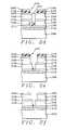
- FIG. 2 ais a partial cross-sectional view of a substrate showing the forming of a via opening in a stack of dielectric layers on the substrate, according to the present invention.
- FIG. 2 bis a partial cross-sectional view of a substrate showing the forming of a composite mask, according to the present invention.
- FIG. 2 cis a partial cross-sectional view of a substrate showing the patterning of a trench opening in a photoresist, according to the present invention.
- FIG. 2 dis a partial cross-sectional view of a substrate showing the forming of the trench opening of FIG. 2 c in the composite mask of the same substrate, according to the present invention.
- FIG. 2 eis a partial cross-sectional view of a substrate showing the transfer of the trench opening in the composite mask of FIG. 2 d into the fourth dielectric layer of the substrate, according to the present invention.
- FIG. 2 fis a partial cross-sectional view of a substrate showing the completion of the dual damascene structure of this invention after the removal of the residual polymer from the via of FIG. 2 e, according to the present invention.
- FIGS. 2 a - 2 fthere is shown a method of forming a composite mask in order to prevent via poisoning, as well as for the multi-purpose of improving the lithographic characteristics in the forming of a dual damascene structure.
- Thisis accomplished by using a mask comprising silicon-based as well as polymeric dielectric layers.
- the polymeric dielectricmakes it possible to protect the via openings by conformally covering the sidewalls of the via and, at the same time, by bringing controllability to the height of the protective dielectric in the via opening.
- the polymeric dielectricalso serves as the main plasma resisting layer during the trench etch, as disclosed below, the required photoresist is much thinner, thereby alleviating the lithography process loading.
- FIG. 2 ashows a portion of a semiconductor substrate ( 200 ), which is preferably silicon having an intermetal dielectric (IMD) layer formed on a substructure of gates and interlevel dielectric layers (ILD) already formed thereon.
- IMDintermetal dielectric
- ILD layersare formed between metal layers which are formed after forming an ILD layer over polysilicon gates and before first metal layer is formed.
- the substrateis provided with a metal layer ( 210 ) and dielectric layer ( 220 ) which serves as a diffusion barrier to the underlying metal layer.
- the barrier layerprotects the pre-existing interconnect layer ( 210 ) from oxidation or corrosion during later process steps.
- the interconnect metalis preferably copper with a thickness between about 2000 to 7000 ⁇
- the barrier layercomprises nitride or carbide with a thickness between about 300 to 1000 ⁇ , which can also serve as an etch-stop layer.
- a low-k dielectric material with a dielectric constant less than 4.0is next spun over, or grown over the barrier layer to form layer ( 230 ), as shown in FIG. 2 a.
- Some of the conventional low-k materialsinclude black diamond, while some others are usually fluorinated, such as the amorphous fluorinated carbon ( ⁇ -C:F), poly-tetra-fluoro-ethylene (PTFE), fluorinated polyimide, fluorinated or SiO 2 , phosphosilicate glass (PSG).
- Some others, such as benzocyclobutene (BCB), hydrogen silsesquioxane (HSQ) or the material known as FLARE manufactured by Allied Signal or SILK manufactured by Dow Chemicalhave even lower dielectric constants.
- the low-k dielectricis black diamond having a thickness between about 2000 to 6000 ⁇ .
- dielectric layer ( 230 )can also comprise an organic low-k material, such as BCB, FLARE, and SILK, and a chemical vapor deposited (CVD) oxide, the combination called a “hybrid low-k” dielectric having a thickness between about 2000 to 6000 ⁇ , where the top organic layer has a thickness between about 1000 to 5000 ⁇ and the lower CVD oxide layer has a thickness between about 200 to 1000 ⁇ .
- these low-k materialsare incompatible with conventional photoresist stripping using oxygen ashers or solvents.
- the patterning of the low-k materials to form the trenches and vias of a damascene formationis a difficult task due to this incompatibility of the low-k materials with conventional photoresist stripping. That is, in most cases, the low-k etch chemistry etches the photoresist at approximately the same rate as the low k dielectric. It is, therefore, a key aspect of the present invention to use a hard mask which would have a low loss when etching the low-k dielectric.
- a full stack of high selectivity materialpreferably, selected from a group consisting of nitride, oxynitride, carbide and other high oxide etch selectivity materials is used, having a thickness between about 200 to 1000 ⁇ .
- layer ( 240 )is used as a hard mask to pattern low-k dielectric layer ( 230 ) with an organic etch.
- layer ( 240 )is nitride or carbide and has a thickness between about 10 to 1000 ⁇ .
- Dielectric layer ( 250 )is also a low-k material, similar to layer ( 230 ), and has a thickness between about 2000 to 6000° C.
- Next dielectric layer ( 260 ), serving as a cap layer, altocomprises nitride or carbide having a thickness between about 200 to 1000 ⁇ .
- a first photoresist layeris formed over the substrate including over the stack of five dielectric layers ( 220 ) through ( 260 ) shown in FIG. 2 a. Then, using the “via-first” or “counter-bore” approach, the photoresist is patterned with a via hole, and via hole ( 265 ) is etched through the stack of dielectric layers reaching first dielectric layer ( 220 ) as shown in the same FIG. 2 a. The etching is accomplished with a recipe comprising C x F y , N 2 , O 2 .)
- a polymeric dielectric layer ( 270 ), preferably SiLK by Dow Chemicalis first spun on the substrate to a thickness between about 1000 to 5000 ⁇ .
- the spun-on polymer over the substratefills via opening ( 265 ) completely, and it especially has the property of filling conformally and well small openings in high scale integration of sub-micron technologies. Because of its conformal filling capabilities, it will be apparent at a later step that it will be possible to retain a portion of the polymeric dielectric in the via opening as a protective cover during the subsequent process steps.
- silicon-based dielectric layer ( 280 )is deposited over layer ( 270 ) as shown in FIG. 2 b. It is preferred that layer ( 280 ) is selected from a group consisting of silicon oxynitride (SiON), silicon nitride (SiN) and SiO x and that it has a thickness between about 200 to 1000 ⁇ . Then photoresist layer ( 290 ) is formed over the silicon-based dielectric layer to perform trench photolithography.
- the required thickness of photoresist layer ( 290 )is only between about 1000 to 3000 ⁇ so that, thereby alleviating the well-known lithography process loading, that is, extending the lithography process window.
- the photoresistis then patterned with trench opening ( 295 ) (shown in FIG. 2 c ) and the opening is etched into the underlying silicon-based layer ( 280 ) which will be used as a hard mask for etching the trench opening into the low-k dielectric layer on the substrate.
- the trench patternis defined in the polymeric dielectric by etching the pattern using an oxygen, (O 2 ) or nitrogen/hydrogen (N 2 /H 2 ) based plasma etch, as shown in FIG. 2 d.
- a portion of the polymeric dielectricis left in via opening ( 265 ).
- height ( 275 ) of the remaining portionis between about 1000 to 4000 ⁇ so that when the trench etch is performed at the next step, the corner edge of the via will avoid, what is called “polymer fence” and not be faceted, that is, it will have a well defined corner. Also, the presence of the polymeric dielectric in the via provides protection from via poisoning that would otherwise be caused by the interaction between the outgassing from the sidewalls of the via and the photoresist.
- trench etchis performed with a recipe comprising C x F y , N 2 , O 2 such that trench opening ( 295 ) is transferred into dielectric layer ( 250 ) comprising low-k material and stopping on middle etch-stop layer ( 240 ).
- any polymeric dielectric material remaining in the via openingis removed, that is cleaned up completely by using oxygen plasma ashing as shown in FIG. 2 f.
- the dual damascene structure so completedis now ready for further processing to fill with metal to form the desired interconnect to the underlying first metal layer, layer ( 210 ).
Landscapes
- Engineering & Computer Science (AREA)
- Physics & Mathematics (AREA)
- Condensed Matter Physics & Semiconductors (AREA)
- General Physics & Mathematics (AREA)
- Manufacturing & Machinery (AREA)
- Computer Hardware Design (AREA)
- Microelectronics & Electronic Packaging (AREA)
- Power Engineering (AREA)
- Chemical & Material Sciences (AREA)
- Inorganic Chemistry (AREA)
- Internal Circuitry In Semiconductor Integrated Circuit Devices (AREA)
Abstract
Description
(1) Field of the Invention
The present invention relates to the manufacture of semiconductor devices in general, and in particular, to a method of dual damascene patterning using a multi-purpose composite mask.
(2) Description of the Related Art
In forming dual a damascene structure, via protection is important especially in using the via-first approach, which is explained more in detail below. In this via-first (or, counter-bore) approach, the typical via protection materials are organic, such as photoresist or anti-reflection coating (ARC). It is usually difficult to have a conformal filling of the via with this type of filler materials, especially for small geometry features where consistent filling height is sought. In addition, these organic materials react with the outgassing that occurs from the sidewalls of the vias, thus causing via poisoning. It is disclosed later in the embodiments of the present invention a method of alleviating these via filling problems.
The term ‘damascene’ is derived from a form of inlaid metal jewelry. In the context of integrated circuits it implies a patterned layer imbedded on and in another layer such that the top surfaces of the two layers are coplanar. Thus, in semiconductor manufacturing, trenches and holes in appropriate locations in the trenches are formed in an insulative material by etching, which are then filled with metal. Metal in trenches form the horizontal metal line interconnects while the metal in the underlying holes form the vertical connections to the layers of metal interconnects formed in the previous damascene structure.
Thus, in a single damascene semiconductor manufacturing process, incisions, or trenches, are formed in an insulative layer and filled with metal to form conductive lines. Dual damascene takes the process one step further in that, in addition to forming the trenches of a single damascene, hole openings are also formed at appropriate places in the trench further into the insulative layer. The resulting composite structure of trenches and holes are filled with metal. The process is repeated as many times as required to form the multi-level interconnections between metal lines and the holes formed therebetween.
In one approach for a dual damascene process shown in FIG. 1a,two insulative layers (120) and (130), sometimes referred to as intermetal dielectrics (IMD), are formed on a substrate (100) with an intervening etch-stop or trench-stop layer (125). Substrate (100) is provided with metal layer (110) and another etch-stop layer or via-stop liner (115). Metal layer can be the commonly used aluminum or copper, while the liner can be another dielectric layer. A desired trench or trench pattern (150) is first etched into the upper insulative material (130) using conventional photolithographic methods and photoresist (140). The etching stops on trench-stop layer (125). Next, a second photoresist layer (160) is formed over the substrate, thus filling the trench opening (150), and patterned with hole opening (170), as shown in FIG. 1b.The hole pattern is then etched into the lower insulative layer (120) as shown in FIG. 1cand photoresist removed, thus forming the dual damascene structure shown in FIG. 1f.
Or, the order in which the trench and the hole are formed can be reversed so that the hole is formed first, which is called the “via-first” process. The fact that the trench is formed later over the hole, the process is sometimes referred to as “counter-bore” as in forming a counter-bore for a screw. Thus, the upper insulative layer (130) is first etched, or patterned, with hole (170), as shown in FIG. 1d.The hole pattern is also formed into etch-stop layer (125). Then, the upper layer is etched to form trench (150) while at the same time the etching transfers the hole pattern in the etch-stop layer into lower insulation layer (120), as shown in FIG. 1e.It will be noted that trench-stop layer (125) stops the etching of the trench into the lower insulation layer. Similarly, via-stop layer (115) also stops etching. However, layer (115) at the bottom of opening (170) is removed before metal is deposited at the next step. Thus, after the completion of the thusly formed dual damascene structure, both the hole opening and trench opening are filled with metal (180), and any excess material on the surface of the substrate is removed by chemical mechanical polishing, as seen in FIG. 1f.
In prior art, various methods of forming damascene structures are described. In U.S. Pat. No. 6,074,942, Lou describes a method for forming a dual damascene contact and interconnect with the steps of: forming an insulating layer on a substrate; forming a nitride layer over said insulating layer; forming a cap oxide layer over said nitride layer; patterning and etching said insulating layer, nitride layer, and cap oxide layer to correspond to the location of said contacts; patterning and etching said nitride layer and said cap oxide layer to correspond to the pattern of said interconnects; and performing a reflow step.
In U.S. Pat. No. 6,083,822, Lee discloses a fabrication process for a copper dual damascene structure where a composite insulator layer, comprising silicon oxide layers, and multiple silicon nitride layers as stop layers are used. A method of forming a self-aligned dual damascene structure is described by Wang, et al., in U.S. Pat. Nos. 6,207,576 and 6,207,577. A nitride etch stop layer is formed on an oxide layer on a substrate, and a low k dielectric layer is formed on the nitride etch stop layer. A trench is etched into the low k dielectric layer, followed by the etching of a via into the oxide dielectric layer. The oxide dielectric material and low k dielectric material are selected so that they have different sensitivity to at least one etchant chemistry. Undercutting in the second dielectric layer caused by over etching is prevented during the etching of the via in the second dielectric layer by employing an etch chemistry that etches only the oxide dielectric material and not the low k dielectric material.
In another U.S. Pat. No. 6,042,999 by Line, et al., a robust damascene process is disclosed where the substructure in a substrate is protected from damage caused by multiple etchings required in a damascene process by filling a contact or via hole opening with a protective material prior to the forming of the conductive line opening of the damascene structure having an etch-stop layer separating a lower and an upper dielectric layer. In a first embodiment, the protective material is partially removed from the hole opening reaching the substructure prior to the forming of the upper conductive line opening by etching. In the second embodiment, the protective material in the hole is removed at the same time the upper conductive line opening is formed by etching. In a third embodiment, the disclosed process is applied without the need for an etch-stop layer.
A dual damascene with a sacrificial via fill is described in U.S. Pat. No. 5,705,430 by Avanzino, et al. A first layer of insulating material is formed with via openings. The openings are filled with a sacrificial removable material. A second layer of insulating material is deposed on the first layer. In one embodiment, the etch selectivity to the etchant of the second layer is essentially the same as the sacrificial via fill and is substantially higher than second layer. Using a conductive line pattern aligned with the via openings, conductive line openings are etched in the second insulating layer and, during etching. The sacrificial fill is removed from the via openings. In a second embodiment, the sacrificial material is not etchable by the etchant for forming the conductive line openings and, after formation of the conductive line openings, the sacrificial material is removed with an etchant to which the first insulating layer is resistive or less selective. A conductive material now is deposited in the conductive line and via openings.
A method for making metal interconnections and buried metal plug structures for multilevel interconnections on semiconductor integrated circuits is disclosed in U.S. Pat. No. 5,702,982. The method utilizes a single patterned photoresist layer for etching trenches in an insulating layer, while at the same time protecting the device contact areas in the contact openings from being etched, thereby reducing process complexity and manufacturing cost. After the trenches arc formed, die patterned photoresist layer and the photoresist in the contact openings are removed by plasma ashing and a metal layer is deposited and etched back or chemical-mechanical polished to form concurrently the metal interconnections and the buried metal plug contacts. The surface of the metal interconnections is coplanar with the insulating surface, thereby allowing the process to be repeated several times to complete the necessary multilevel of metal wiring needed to wire-up the integrated circuits while maintaining a planar surface.
A different method of forming a damascene structure is disclosed later in the embodiments of the present invention where some of the prior art problems of filling vias are alleviated.
It is therefore an object of this invention to provide a method of forming a multi-purpose composite mask for patterning dual damascene structures.
It is another object of the present invention to provide a method of using certain dielectric materials in order to achieve conformally filled via openings, especially those with small geometry features, in order to prevent via poisoning resulting from outgassing from unprotected walls of the openings.
It is yet another object of the present invention to provide a method of forming a composite mask for serving not only to prevent via poisoning, but for the multi-purpose of also improving the lithographic characteristics of forming a dual damascene structure.
It is still another object of the present invention to provide a method for better controlling the conformity on the sidewalls as well as the height in the via opening of the via protection material in order to improve the characteristics of the resulting dual damascene structure.
These objects are accomplished by providing a substrate having a stack of dielectric layers comprising a barrier layer, a first dielectric layer, an etch-stop layer, a second dielectric layer and a cap layer formed thereon in said order; forming a via opening in said stack of dielectric layers; forming a polymeric dielectric layer over said substrate, including over said via opening; forming a silicon based dielectric layer over said polymeric dielectric layer; patterning said silicon based and polymeric dielectric layers to define a trench opening, and partially removing said polymeric dielectric layer from said via opening; using said polymeric dielectric as a via protector, etching further said trench opening until said etch-stop layer is reached; and leaning any remaining polymeric dielectric in said via to complete the forming of said dual damascene structure.
FIGS. 1a-1cshow the forming of a dual damascene structure where a trench opening is etched first into an upper second dielectric layer until an etch-stop layer is reached, and then the hole pattern etched into the lower first dielectric layer, according to prior art.
FIGS. 1d-1eshow the forming of a dual damascene structure with “via-first”, or, “counter-bore” approach where a via opening is etched first into an upper second dielectric layer until an etch-stop layer is reached, and then the trench opening etched into the top layer while at the same time the via opening is transferred into the lower first dielectric layer, according to prior art.
FIG. 1fshows a dual damascene structure formed by either one of the methods shown in FIGS. 1a-1cor FIGS. 1d-1e,according to prior art.
FIG. 2ais a partial cross-sectional view of a substrate showing the forming of a via opening in a stack of dielectric layers on the substrate, according to the present invention.
FIG. 2bis a partial cross-sectional view of a substrate showing the forming of a composite mask, according to the present invention.
FIG. 2cis a partial cross-sectional view of a substrate showing the patterning of a trench opening in a photoresist, according to the present invention.
FIG. 2dis a partial cross-sectional view of a substrate showing the forming of the trench opening of FIG. 2cin the composite mask of the same substrate, according to the present invention.
FIG. 2eis a partial cross-sectional view of a substrate showing the transfer of the trench opening in the composite mask of FIG. 2dinto the fourth dielectric layer of the substrate, according to the present invention.
FIG. 2fis a partial cross-sectional view of a substrate showing the completion of the dual damascene structure of this invention after the removal of the residual polymer from the via of FIG. 2e,according to the present invention.
Referring now to the drawings, FIGS. 2a-2f,there is shown a method of forming a composite mask in order to prevent via poisoning, as well as for the multi-purpose of improving the lithographic characteristics in the forming of a dual damascene structure. This is accomplished by using a mask comprising silicon-based as well as polymeric dielectric layers. Thus, one of the components of the composite mask, namely, the polymeric dielectric, makes it possible to protect the via openings by conformally covering the sidewalls of the via and, at the same time, by bringing controllability to the height of the protective dielectric in the via opening. In addition, because the polymeric dielectric also serves as the main plasma resisting layer during the trench etch, as disclosed below, the required photoresist is much thinner, thereby alleviating the lithography process loading.
More specifically, FIG. 2ashows a portion of a semiconductor substrate (200), which is preferably silicon having an intermetal dielectric (IMD) layer formed on a substructure of gates and interlevel dielectric layers (ILD) already formed thereon. It will be understood by those skilled in the art that IMD layers are formed between metal layers which are formed after forming an ILD layer over polysilicon gates and before first metal layer is formed. In FIG. 2a,the substrate is provided with a metal layer (210) and dielectric layer (220) which serves as a diffusion barrier to the underlying metal layer. The barrier layer protects the pre-existing interconnect layer (210) from oxidation or corrosion during later process steps. The interconnect metal is preferably copper with a thickness between about 2000 to 7000 Å, and the barrier layer comprises nitride or carbide with a thickness between about 300 to 1000 Å, which can also serve as an etch-stop layer.
A low-k dielectric material with a dielectric constant less than 4.0 is next spun over, or grown over the barrier layer to form layer (230), as shown in FIG. 2a.Some of the conventional low-k materials include black diamond, while some others are usually fluorinated, such as the amorphous fluorinated carbon (α-C:F), poly-tetra-fluoro-ethylene (PTFE), fluorinated polyimide, fluorinated or SiO2, phosphosilicate glass (PSG). Some others, such as benzocyclobutene (BCB), hydrogen silsesquioxane (HSQ) or the material known as FLARE manufactured by Allied Signal or SILK manufactured by Dow Chemical have even lower dielectric constants. In the preferred embodiment, the low-k dielectric is black diamond having a thickness between about 2000 to 6000 Å. It will be understood that dielectric layer (230) can also comprise an organic low-k material, such as BCB, FLARE, and SILK, and a chemical vapor deposited (CVD) oxide, the combination called a “hybrid low-k” dielectric having a thickness between about 2000 to 6000 Å, where the top organic layer has a thickness between about 1000 to 5000 Å and the lower CVD oxide layer has a thickness between about 200 to 1000 Å.
In many cases, these low-k materials are incompatible with conventional photoresist stripping using oxygen ashers or solvents. Thus, the patterning of the low-k materials to form the trenches and vias of a damascene formation is a difficult task due to this incompatibility of the low-k materials with conventional photoresist stripping. That is, in most cases, the low-k etch chemistry etches the photoresist at approximately the same rate as the low k dielectric. It is, therefore, a key aspect of the present invention to use a hard mask which would have a low loss when etching the low-k dielectric. For this purpose, a full stack of high selectivity material, preferably, selected from a group consisting of nitride, oxynitride, carbide and other high oxide etch selectivity materials is used, having a thickness between about 200 to 1000 Å. Thus, layer (240) is used as a hard mask to pattern low-k dielectric layer (230) with an organic etch.
A third dielectric layer (240), which also serves as an etch-stop layer, is formed over layer (230). Preferably layer (240) is nitride or carbide and has a thickness between about 10 to 1000 Å. Dielectric layer (250) is also a low-k material, similar to layer (230), and has a thickness between about 2000 to 6000° C. Next dielectric layer (260), serving as a cap layer, alto comprises nitride or carbide having a thickness between about 200 to 1000 Å.
A first photoresist layer, not shown, is formed over the substrate including over the stack of five dielectric layers (220) through (260) shown in FIG. 2a.Then, using the “via-first” or “counter-bore” approach, the photoresist is patterned with a via hole, and via hole (265) is etched through the stack of dielectric layers reaching first dielectric layer (220) as shown in the same FIG. 2a.The etching is accomplished with a recipe comprising CxFy, N2, O2.)
After the first via etch, trench etch is performed next. However, as a main feature and key aspect of the instant invention, multi-dielectric deposition is used to form a multi-purpose mask prior to etching the trench. Namely, a polymeric dielectric layer (270), preferably SiLK by Dow Chemical is first spun on the substrate to a thickness between about 1000 to 5000 Å. It will be noted that the spun-on polymer over the substrate fills via opening (265) completely, and it especially has the property of filling conformally and well small openings in high scale integration of sub-micron technologies. Because of its conformal filling capabilities, it will be apparent at a later step that it will be possible to retain a portion of the polymeric dielectric in the via opening as a protective cover during the subsequent process steps.
At the next step, silicon-based dielectric layer (280) is deposited over layer (270) as shown in FIG. 2b.It is preferred that layer (280) is selected from a group consisting of silicon oxynitride (SiON), silicon nitride (SiN) and SiOxand that it has a thickness between about 200 to 1000 Å. Then photoresist layer (290) is formed over the silicon-based dielectric layer to perform trench photolithography. It will be noted that because of the underlying composite mask comprising silicon-based and polymeric layers (280) and (2870), respectively, the required thickness of photoresist layer (290) is only between about 1000 to 3000 Å so that, thereby alleviating the well-known lithography process loading, that is, extending the lithography process window.
The photoresist is then patterned with trench opening (295) (shown in FIG. 2c) and the opening is etched into the underlying silicon-based layer (280) which will be used as a hard mask for etching the trench opening into the low-k dielectric layer on the substrate. However, first, the trench pattern is defined in the polymeric dielectric by etching the pattern using an oxygen, (O2) or nitrogen/hydrogen (N2/H2) based plasma etch, as shown in FIG. 2d.At the same time, a portion of the polymeric dielectric is left in via opening (265). It is very critical that height (275) of the remaining portion is between about 1000 to 4000 Å so that when the trench etch is performed at the next step, the corner edge of the via will avoid, what is called “polymer fence” and not be faceted, that is, it will have a well defined corner. Also, the presence of the polymeric dielectric in the via provides protection from via poisoning that would otherwise be caused by the interaction between the outgassing from the sidewalls of the via and the photoresist.
Thus, using the composite mask of layers (280) and (270) as a hard mask, at the next step, trench etch is performed with a recipe comprising CxFy, N2, O2such that trench opening (295) is transferred into dielectric layer (250) comprising low-k material and stopping on middle etch-stop layer (240). Subsequently, any polymeric dielectric material remaining in the via opening is removed, that is cleaned up completely by using oxygen plasma ashing as shown in FIG. 2f.The dual damascene structure so completed is now ready for further processing to fill with metal to form the desired interconnect to the underlying first metal layer, layer (210).
Though these numerous details of the disclosed method are set forth here, such as process parameters, to provide an understanding of the present invention, it will be obvious, however, to those skilled in the art that these specific details need not be employed to practice the present invention. At the same time, it will be evident that the same methods may be employed in other similar process steps that are too many to cite, such as in filling vias with other polymers having good filling properties.
While the invention has been particularly shown and described with reference to the preferred embodiments thereof, it will be understood by those skilled in the art that various changes in form and details may be made without departing from the spirit and scope of the. invention.
Claims (34)
1. A method of forming a multi-purpose composite mask for dual damascene patterning comprising the steps of:
providing a substrate having a stack of dielectric layers comprising a barrier layer, a first dielectric layer, an etch-stop layer, a second dielectric layer and a cap layer formed thereon in said order wherein said first dielectric layer comprises a low-k material including black diamond;
forming a via opening in said stack of dielectric layers;
forming a polymeric dielectric layer over said substrate, including over said via opening;
forming a silicon based dielectric layer over said polymeric dielectric layer;
patterning said silicon based and polymeric dielectric layers to define a trench opening, and partially removing said polymeric dielectric layer from said via opening;
using said polymeric dielectric as a via protector, etching further said trench opening until said etch-stop layer is reached; and
cleaning any remaining polymeric dielectric in said via to complete the forming of said dual damascene structure.
2. The method according toclaim 1 , wherein said barrier layer comprises nitride or a carbide.
3. The method according toclaim 1 , wherein said barrier layer has a thickness between about 200 to 1000 Å.
4. The method according toclaim 1 , wherein said first dielectric has a thickness between about 2000 to 6000 Å.
5. The method according toclaim 1 , wherein said etch-stop layer comprises nitride or carbide.
6. The method according toclaim 1 , wherein said etch-stop layer has a thickness between about 200 to 6000 Å.
7. The method according toclaim 1 , wherein said second dielectric layer comprises a low-k material including black diamond.
8. The method according toclaim 1 , wherein said second dielectric has a thickness between about 2000 to 6000 Å.
9. The method according toclaim 1 , wherein said cap layer comprises nitride or carbide.
10. The method according toclaim 1 , wherein said cap layer has a thickness between about 200 to 1000 Å.
11. The method according toclaim 1 , wherein said via opening is accomplished with an etch recipe comprising CxFy, N2, and O2.
12. The method according toclaim 1 , wherein said polymeric dielectric layer has a thickness between about 1000 to 5000 Å.
13. The method according toclaim 1 , wherein said silicon based dielectric layer comprises SiON, SiN, or siOx.
14. The method according toclaim 1 , wherein said silicon based dielectric layer has a thickness between about 200 to 1000 Å.
15. The method according toclaim 1 , wherein said patterning to define said trench opening is accomplished with a recipe comprising O2 or N2/H2 based plasma.
16. The method according toclaim 1 , wherein said etching further said trench opening until said etch-stop layer is reached is accomplished with a recipe comprising CxFy, N2, and O2.
17. The method according toclaim 1 , wherein said cleaning said remaining polymeric dielectric is accomplished by oxygen plasma ashing.
18. A method of forming a multi-purpose composite mask for dual damascene patterning comprising the steps of:
providing a substrate having a first metal layer formed thereon;
forming a first dielectric layer over said first metal layer;
forming a second dielectric layer over said first dielectric layer wherein said second dielectric layer comprises a low-k material including black diamond;
forming a third dielectric layer over said second dielectric layer;
forming a fourth dielectric layer over said third dielectric layer;
forming a fifth dielectric layer over said fourth dielectric layer;
forming a via opening starting from said fifth dielectric layer until reaching to and stopping on said first dielectric layer on said substrate;
forming a polymeric dielectric layer over said substrate, including over said via opening;
forming a silicon based dielectric layer over said polymeric dielectric layer;
patterning said silicon based dielectric layer to define a hard mask for trench opening;
using said silicon based dielectric layer as a hard mask, etching to transfer said trench opening into said polymeric dielectric layer, while at the same time leaving a portion of said polymeric dielectric in said via opening;
using said silicon based and polymeric dielectric layers as a mask, further trench etching the underlying said fifth and fourth dielectric layers until stopping on said third dielectric layer; and
removing said portion of said polymeric dielectric from the bottom of said via opening until said first dielectric via is reached, and said dual damascene structure is formed.
19. The method according toclaim 18 , wherein said first dielectric layer is a barrier layer comprising nitride or a carbide.
20. The method according toclaim 18 , wherein said first dielectric layer has a thickness between about 200 to 1000 Å.
21. The method according toclaim 18 , wherein said second dielectric has a thickness between about 2000 to 6000 Å.
22. The method according toclaim 18 , wherein said third dielectric layer is an etch-stop layer comprising nitride or carbide.
23. The method according toclaim 18 , wherein said third dielectric layer has a thickness between about 200 to 1000 Å.
24. The method according toclaim 18 , wherein said fourth dielectric layer comprises a low-k material including black diamond.
25. The method according toclaim 18 , wherein said fourth dielectric has a thickness between about 2000 to 6000 Å.
26. The method according toclaim 18 , wherein said fifth dielectric layer is a cap layer comprising nitride or carbide.
27. The method according toclaim 18 , wherein said fifth dielectric layer has a thickness between about 200 to 1000 Å.
28. The method according toclaim 18 , wherein said via opening is accomplished with an etch recipe comprising CxFy, N2, and O2.
29. The method according toclaim 18 , wherein said polymeric dielectric layer has a thickness between about 1000 to 5000 Å.
30. The method according toclaim 18 , wherein said silicon based dielectric layer comprises SiON, SiN, or SiOx.
31. The method according toclaim 18 , wherein said silicon based dielectric layer has a thickness between about 200 to 1000 Å.
32. The method according toclaim 18 , wherein said patterning to define for said trench opening is accomplished with a recipe comprising O2 or N2/H2 based plasma.
33. The method according toclaim 18 , wherein said further trench etching until stopping on said third dielectric layer is accomplished with a recipe comprising CxFy, N2, and O2.
34. The method according toclaim 18 , wherein said removing said portion of said polymeric dielectric is accomplished by oxygen plasma ashing.
Priority Applications (1)
| Application Number | Priority Date | Filing Date | Title |
|---|---|---|---|
| US10/184,790US6689695B1 (en) | 2002-06-28 | 2002-06-28 | Multi-purpose composite mask for dual damascene patterning |
Applications Claiming Priority (1)
| Application Number | Priority Date | Filing Date | Title |
|---|---|---|---|
| US10/184,790US6689695B1 (en) | 2002-06-28 | 2002-06-28 | Multi-purpose composite mask for dual damascene patterning |
Publications (1)
| Publication Number | Publication Date |
|---|---|
| US6689695B1true US6689695B1 (en) | 2004-02-10 |
Family
ID=30769449
Family Applications (1)
| Application Number | Title | Priority Date | Filing Date |
|---|---|---|---|
| US10/184,790Expired - LifetimeUS6689695B1 (en) | 2002-06-28 | 2002-06-28 | Multi-purpose composite mask for dual damascene patterning |
Country Status (1)
| Country | Link |
|---|---|
| US (1) | US6689695B1 (en) |
Cited By (72)
| Publication number | Priority date | Publication date | Assignee | Title |
|---|---|---|---|---|
| US20030216057A1 (en)* | 2002-05-17 | 2003-11-20 | Hussein Makarem A. | Method integrating polymeric interlayer dielectric in integrated circuits |
| US20040058280A1 (en)* | 2002-09-25 | 2004-03-25 | Samsung Electronics Co., Ltd. | Method for manufacturing a semiconductor device |
| US20040121581A1 (en)* | 2002-12-17 | 2004-06-24 | Abbas Ali | Method of forming dual-damascene structure |
| US20040183203A1 (en)* | 2003-03-20 | 2004-09-23 | Meagley Robert P. | Composite sacrificial material |
| US20040266201A1 (en)* | 2003-06-24 | 2004-12-30 | International Business Machines Corporation | Method for forming damascene structure utilizing planarizing material coupled with diffusion barrier material |
| US20050006340A1 (en)* | 2003-07-10 | 2005-01-13 | Tien-I Bao | Method for preventing formation of photoresist scum |
| US20060046201A1 (en)* | 2004-09-02 | 2006-03-02 | Sandhu Gurtej S | Method to align mask patterns |
| US20060046200A1 (en)* | 2004-09-01 | 2006-03-02 | Abatchev Mirzafer K | Mask material conversion |
| US20060046422A1 (en)* | 2004-08-31 | 2006-03-02 | Micron Technology, Inc. | Methods for increasing photo alignment margins |
| EP1646083A1 (en)* | 2004-10-08 | 2006-04-12 | Interuniversitair Microelektronica Centrum ( Imec) | Alternative dual damascene patterning approach |
| US20060139496A1 (en)* | 2004-12-27 | 2006-06-29 | Sanyo Electric Co., Ltd. | Video signal processing apparatus |
| US20060141777A1 (en)* | 2004-12-23 | 2006-06-29 | Yeong-Sil Kim | Methods for patterning a layer of a semiconductor device |
| US20060163731A1 (en)* | 2005-01-21 | 2006-07-27 | Keishi Inoue | Dual damascene interconnections employing a copper alloy at the copper/barrier interface |
| US20060178002A1 (en)* | 2005-02-05 | 2006-08-10 | Samsung Electronics Co., Ltd. | Methods for forming dual damascene wiring for semiconductor devices using protective via capping layer |
| US20060211260A1 (en)* | 2005-03-15 | 2006-09-21 | Luan Tran | Pitch reduced patterns relative to photolithography features |
| US20060216923A1 (en)* | 2005-03-28 | 2006-09-28 | Tran Luan C | Integrated circuit fabrication |
| DE102005020060A1 (en)* | 2005-04-29 | 2006-11-02 | Advanced Micro Devices, Inc., Sunnyvale | Low-k dielectric layer patterning method for integrated circuits, involves forming patterned hard mask above low-k dielectric layer of semiconductor metallization layer |
| US20060258162A1 (en)* | 2004-09-02 | 2006-11-16 | Abatchev Mirzafer K | Method for integrated circuit fabrication using pitch multiplication |
| US20060263699A1 (en)* | 2005-05-23 | 2006-11-23 | Mirzafer Abatchev | Methods for forming arrays of a small, closely spaced features |
| US20060273456A1 (en)* | 2005-06-02 | 2006-12-07 | Micron Technology, Inc., A Corporation | Multiple spacer steps for pitch multiplication |
| US20060278911A1 (en)* | 2005-06-14 | 2006-12-14 | Eppich Anton P | Relaxed-pitch method of aligning active area to digit line |
| US20060281266A1 (en)* | 2005-06-09 | 2006-12-14 | Wells David H | Method and apparatus for adjusting feature size and position |
| US20070018206A1 (en)* | 2005-07-06 | 2007-01-25 | Leonard Forbes | Surround gate access transistors with grown ultra-thin bodies |
| SG128529A1 (en)* | 2005-06-28 | 2007-01-30 | United Microelectronics Corp | Method for eliminating bridging defect in vial first dual damascene process |
| US20070033098A1 (en)* | 2005-08-05 | 2007-02-08 | International Business Machines Corporation | Method, system and storage medium for creating sales recommendations |
| US20070050748A1 (en)* | 2005-08-30 | 2007-03-01 | Micron Technology, Inc., A Corporation | Method and algorithm for random half pitched interconnect layout with constant spacing |
| US20070049011A1 (en)* | 2005-09-01 | 2007-03-01 | Micron Technology, Inc., A Corporation | Method of forming isolated features using pitch multiplication |
| US20070049040A1 (en)* | 2005-03-15 | 2007-03-01 | Micron Technology, Inc., A Corporation | Multiple deposition for integration of spacers in pitch multiplication process |
| US20070049030A1 (en)* | 2005-09-01 | 2007-03-01 | Sandhu Gurtej S | Pitch multiplication spacers and methods of forming the same |
| US20070049032A1 (en)* | 2005-09-01 | 2007-03-01 | Mirzafer Abatchev | Protective coating for planarization |
| US20070048674A1 (en)* | 2005-09-01 | 2007-03-01 | Wells David H | Methods for forming arrays of small, closely spaced features |
| US20070051997A1 (en)* | 2005-08-31 | 2007-03-08 | Gordon Haller | Semiconductor memory device |
| US20070072406A1 (en)* | 2005-09-28 | 2007-03-29 | Lee Kyoung W | Methods of forming integrated circuit devices having metal interconnect structures therein |
| US20070090363A1 (en)* | 2005-07-25 | 2007-04-26 | Abbott Todd R | Dram including a vertical surround gate transistor |
| US20070105357A1 (en)* | 2005-09-01 | 2007-05-10 | Micron Technology, Inc. | Silicided recessed silicon |
| US7238619B2 (en) | 2005-07-06 | 2007-07-03 | United Microelectronics Corp. | Method for eliminating bridging defect in via first dual damascene process |
| US20070159617A1 (en)* | 2006-01-11 | 2007-07-12 | Mackey Jeffrey L | Photolithographic systems and methods for producing sub-diffraction-limited features |
| US20070205443A1 (en)* | 2006-03-02 | 2007-09-06 | Werner Juengling | Vertical gated access transistor |
| US20070205438A1 (en)* | 2006-03-02 | 2007-09-06 | Werner Juengling | Masking process for simultaneously patterning separate regions |
| US20070238308A1 (en)* | 2006-04-07 | 2007-10-11 | Ardavan Niroomand | Simplified pitch doubling process flow |
| US20070249170A1 (en)* | 2006-04-25 | 2007-10-25 | David Kewley | Process for improving critical dimension uniformity of integrated circuit arrays |
| US20070261016A1 (en)* | 2006-04-24 | 2007-11-08 | Sandhu Gurtej S | Masking techniques and templates for dense semiconductor fabrication |
| US20070275554A1 (en)* | 2003-05-30 | 2007-11-29 | Nec Electronics Corporation | Semiconductor device with interconnection structure for reducing stress migration |
| US20070281219A1 (en)* | 2006-06-01 | 2007-12-06 | Sandhu Gurtej S | Masking techniques and contact imprint reticles for dense semiconductor fabrication |
| US20080057692A1 (en)* | 2006-08-30 | 2008-03-06 | Wells David H | Single spacer process for multiplying pitch by a factor greater than two and related intermediate IC structures |
| US20080064199A1 (en)* | 2006-09-12 | 2008-03-13 | Wan Jae Park | Methods of Forming Electrical Interconnect Structures Using Polymer Residues to Increase Etching Selectivity Through Dielectric Layers |
| US20080070165A1 (en)* | 2006-09-14 | 2008-03-20 | Mark Fischer | Efficient pitch multiplication process |
| CN100378951C (en)* | 2005-07-12 | 2008-04-02 | 联华电子股份有限公司 | Method for manufacturing via-first dual damascene |
| US20080085612A1 (en)* | 2006-10-05 | 2008-04-10 | Micron Technology, Inc. | Method to deposit conformal low temperature SiO2 |
| US20080149593A1 (en)* | 2005-08-25 | 2008-06-26 | Micron Technology, Inc. | Multiple deposition for integration of spacers in pitch multiplication process |
| US7413981B2 (en) | 2005-07-29 | 2008-08-19 | Micron Technology, Inc. | Pitch doubled circuit layout |
| US20080299753A1 (en)* | 2005-09-01 | 2008-12-04 | Figura Thomas A | Peripheral Gate Stacks and Recessed Array Gates |
| US20080299774A1 (en)* | 2007-06-04 | 2008-12-04 | Micron Technology, Inc. | Pitch multiplication using self-assembling materials |
| US20090026572A1 (en)* | 2007-07-25 | 2009-01-29 | Gabriel Dehlinger | Method of Manufacturing a Semiconductor Device, Method of Manufacturing a SOI Device, Semiconductor Device, and SOI Device |
| US20090035665A1 (en)* | 2007-07-31 | 2009-02-05 | Micron Technology, Inc. | Process of semiconductor fabrication with mask overlay on pitch multiplied features and associated structures |
| US20090152645A1 (en)* | 2007-12-18 | 2009-06-18 | Micron Technology, Inc. | Methods for isolating portions of a loop of pitch-multiplied material and related structures |
| CN101609814A (en)* | 2008-06-17 | 2009-12-23 | 三星电子株式会社 | Method for forming semiconductor device and memory system |
| US7659208B2 (en) | 2007-12-06 | 2010-02-09 | Micron Technology, Inc | Method for forming high density patterns |
| US20100062579A1 (en)* | 2008-09-11 | 2010-03-11 | Micron Technology, Inc. | Self-aligned trench formation |
| US7687342B2 (en) | 2005-09-01 | 2010-03-30 | Micron Technology, Inc. | Method of manufacturing a memory device |
| US20100130016A1 (en)* | 2008-11-24 | 2010-05-27 | Micron Technology, Inc. | Methods of forming a masking pattern for integrated circuits |
| US7737039B2 (en) | 2007-11-01 | 2010-06-15 | Micron Technology, Inc. | Spacer process for on pitch contacts and related structures |
| US7829262B2 (en) | 2005-08-31 | 2010-11-09 | Micron Technology, Inc. | Method of forming pitch multipled contacts |
| CN101645414B (en)* | 2008-08-04 | 2011-05-04 | 中芯国际集成电路制造(北京)有限公司 | Double-embedded structure forming method |
| US20110121383A1 (en)* | 2005-05-13 | 2011-05-26 | Micron Technology, Inc. | Memory array with surrounding gate access transistors and capacitors with global and staggered local bit lines |
| US20110165744A1 (en)* | 2005-05-13 | 2011-07-07 | Micron Technology | Memory array with ultra-thin etched pillar surround gate access transistors and buried data/bit lines |
| CN102201365A (en)* | 2010-03-22 | 2011-09-28 | 中芯国际集成电路制造(上海)有限公司 | Method for producing semiconductor device |
| US8030218B2 (en) | 2008-03-21 | 2011-10-04 | Micron Technology, Inc. | Method for selectively modifying spacing between pitch multiplied structures |
| US8076208B2 (en) | 2008-07-03 | 2011-12-13 | Micron Technology, Inc. | Method for forming transistor with high breakdown voltage using pitch multiplication technique |
| US8114573B2 (en) | 2006-06-02 | 2012-02-14 | Micron Technology, Inc. | Topography based patterning |
| US20180005937A1 (en)* | 2016-06-30 | 2018-01-04 | International Business Machines Corporation | Enhanced self-alignment of vias for a semiconductor device |
| US11322362B2 (en) | 2018-11-30 | 2022-05-03 | Taiwan Semiconductor Manufacturing Co., Ltd. | Landing metal etch process for improved overlay control |
Citations (10)
| Publication number | Priority date | Publication date | Assignee | Title |
|---|---|---|---|---|
| US5702982A (en) | 1996-03-28 | 1997-12-30 | Taiwan Semiconductor Manufacturing Company, Ltd. | Method for making metal contacts and interconnections concurrently on semiconductor integrated circuits |
| US5705430A (en) | 1995-06-07 | 1998-01-06 | Advanced Micro Devices, Inc. | Dual damascene with a sacrificial via fill |
| US6042999A (en) | 1998-05-07 | 2000-03-28 | Taiwan Semiconductor Manufacturing Company | Robust dual damascene process |
| US6074942A (en) | 1998-06-03 | 2000-06-13 | Worldwide Semiconductor Manufacturing Corporation | Method for forming a dual damascene contact and interconnect |
| US6083822A (en) | 1999-08-12 | 2000-07-04 | Industrial Technology Research Institute | Fabrication process for copper structures |
| US6100184A (en)* | 1997-08-20 | 2000-08-08 | Sematech, Inc. | Method of making a dual damascene interconnect structure using low dielectric constant material for an inter-level dielectric layer |
| US6207577B1 (en) | 1999-01-27 | 2001-03-27 | Advanced Micro Devices, Inc. | Self-aligned dual damascene arrangement for metal interconnection with oxide dielectric layer and low k dielectric constant layer |
| US6207576B1 (en) | 1999-01-05 | 2001-03-27 | Advanced Micro Devices, Inc. | Self-aligned dual damascene arrangement for metal interconnection with low k dielectric constant materials and oxide etch stop layer |
| US6514860B1 (en)* | 2001-01-31 | 2003-02-04 | Advanced Micro Devices, Inc. | Integration of organic fill for dual damascene process |
| US6521542B1 (en)* | 2000-06-14 | 2003-02-18 | International Business Machines Corp. | Method for forming dual damascene structure |
- 2002
- 2002-06-28USUS10/184,790patent/US6689695B1/ennot_activeExpired - Lifetime
Patent Citations (10)
| Publication number | Priority date | Publication date | Assignee | Title |
|---|---|---|---|---|
| US5705430A (en) | 1995-06-07 | 1998-01-06 | Advanced Micro Devices, Inc. | Dual damascene with a sacrificial via fill |
| US5702982A (en) | 1996-03-28 | 1997-12-30 | Taiwan Semiconductor Manufacturing Company, Ltd. | Method for making metal contacts and interconnections concurrently on semiconductor integrated circuits |
| US6100184A (en)* | 1997-08-20 | 2000-08-08 | Sematech, Inc. | Method of making a dual damascene interconnect structure using low dielectric constant material for an inter-level dielectric layer |
| US6042999A (en) | 1998-05-07 | 2000-03-28 | Taiwan Semiconductor Manufacturing Company | Robust dual damascene process |
| US6074942A (en) | 1998-06-03 | 2000-06-13 | Worldwide Semiconductor Manufacturing Corporation | Method for forming a dual damascene contact and interconnect |
| US6207576B1 (en) | 1999-01-05 | 2001-03-27 | Advanced Micro Devices, Inc. | Self-aligned dual damascene arrangement for metal interconnection with low k dielectric constant materials and oxide etch stop layer |
| US6207577B1 (en) | 1999-01-27 | 2001-03-27 | Advanced Micro Devices, Inc. | Self-aligned dual damascene arrangement for metal interconnection with oxide dielectric layer and low k dielectric constant layer |
| US6083822A (en) | 1999-08-12 | 2000-07-04 | Industrial Technology Research Institute | Fabrication process for copper structures |
| US6521542B1 (en)* | 2000-06-14 | 2003-02-18 | International Business Machines Corp. | Method for forming dual damascene structure |
| US6514860B1 (en)* | 2001-01-31 | 2003-02-04 | Advanced Micro Devices, Inc. | Integration of organic fill for dual damascene process |
Non-Patent Citations (1)
| Title |
|---|
| IBM Tech. Discl. Bull. vol. 30, No. 7, pp. 128-129 (Dec. 1987). (Disclosure Text , 1 page only).* |
Cited By (290)
| Publication number | Priority date | Publication date | Assignee | Title |
|---|---|---|---|---|
| US20030216057A1 (en)* | 2002-05-17 | 2003-11-20 | Hussein Makarem A. | Method integrating polymeric interlayer dielectric in integrated circuits |
| US6774037B2 (en)* | 2002-05-17 | 2004-08-10 | Intel Corporation | Method integrating polymeric interlayer dielectric in integrated circuits |
| US7083899B2 (en)* | 2002-09-25 | 2006-08-01 | Samsung Electronics Co., Ltd. | Method for manufacturing a semiconductor device |
| US20040058280A1 (en)* | 2002-09-25 | 2004-03-25 | Samsung Electronics Co., Ltd. | Method for manufacturing a semiconductor device |
| US6774031B2 (en)* | 2002-12-17 | 2004-08-10 | Texas Instruments Incorporated | Method of forming dual-damascene structure |
| US20040121581A1 (en)* | 2002-12-17 | 2004-06-24 | Abbas Ali | Method of forming dual-damascene structure |
| US20040183203A1 (en)* | 2003-03-20 | 2004-09-23 | Meagley Robert P. | Composite sacrificial material |
| US6858528B2 (en)* | 2003-03-20 | 2005-02-22 | Intel Corporation | Composite sacrificial material |
| US20050124152A1 (en)* | 2003-03-20 | 2005-06-09 | Meagley Robert P. | Composite sacrificial material |
| US7018920B2 (en)* | 2003-03-20 | 2006-03-28 | Intel Corporation | Composite sacrificial material |
| US20070275554A1 (en)* | 2003-05-30 | 2007-11-29 | Nec Electronics Corporation | Semiconductor device with interconnection structure for reducing stress migration |
| US7807567B2 (en)* | 2003-05-30 | 2010-10-05 | Nec Electronics Corporation | Semiconductor device with interconnection structure for reducing stress migration |
| US20040266201A1 (en)* | 2003-06-24 | 2004-12-30 | International Business Machines Corporation | Method for forming damascene structure utilizing planarizing material coupled with diffusion barrier material |
| US7326651B2 (en)* | 2003-06-24 | 2008-02-05 | International Business Machines Corporation | Method for forming damascene structure utilizing planarizing material coupled with compressive diffusion barrier material |
| US20050079701A1 (en)* | 2003-06-24 | 2005-04-14 | International Business Machines Corporation | Method for forming damascene structure utilizing planarizing material coupled with compressive diffusion barrier material |
| US7030031B2 (en)* | 2003-06-24 | 2006-04-18 | International Business Machines Corporation | Method for forming damascene structure utilizing planarizing material coupled with diffusion barrier material |
| US20050006340A1 (en)* | 2003-07-10 | 2005-01-13 | Tien-I Bao | Method for preventing formation of photoresist scum |
| US7015136B2 (en)* | 2003-07-10 | 2006-03-21 | Taiwan Semiconductor Manufacturing Co., Ltd. | Method for preventing formation of photoresist scum |
| US7361569B2 (en) | 2004-08-31 | 2008-04-22 | Micron Technology, Inc. | Methods for increasing photo-alignment margins |
| US20060046422A1 (en)* | 2004-08-31 | 2006-03-02 | Micron Technology, Inc. | Methods for increasing photo alignment margins |
| US7151040B2 (en) | 2004-08-31 | 2006-12-19 | Micron Technology, Inc. | Methods for increasing photo alignment margins |
| US8030222B2 (en) | 2004-08-31 | 2011-10-04 | Round Rock Research, Llc | Structures with increased photo-alignment margins |
| US7368362B2 (en) | 2004-08-31 | 2008-05-06 | Micron Technology, Inc. | Methods for increasing photo alignment margins |
| US7268054B2 (en) | 2004-08-31 | 2007-09-11 | Micron Technology, Inc. | Methods for increasing photo-alignment margins |
| US20060228854A1 (en)* | 2004-08-31 | 2006-10-12 | Luan Tran | Methods for increasing photo alignment margins |
| US20060264000A1 (en)* | 2004-08-31 | 2006-11-23 | Luan Tran | Methods for increasing photo-alignment margins |
| US8486610B2 (en) | 2004-09-01 | 2013-07-16 | Micron Technology, Inc. | Mask material conversion |
| US20060046200A1 (en)* | 2004-09-01 | 2006-03-02 | Abatchev Mirzafer K | Mask material conversion |
| US7910288B2 (en) | 2004-09-01 | 2011-03-22 | Micron Technology, Inc. | Mask material conversion |
| US8895232B2 (en) | 2004-09-01 | 2014-11-25 | Micron Technology, Inc. | Mask material conversion |
| US7629693B2 (en) | 2004-09-02 | 2009-12-08 | Micron Technology, Inc | Method for integrated circuit fabrication using pitch multiplication |
| US7435536B2 (en) | 2004-09-02 | 2008-10-14 | Micron Technology, Inc. | Method to align mask patterns |
| US20060262511A1 (en)* | 2004-09-02 | 2006-11-23 | Abatchev Mirzafer K | Method for integrated circuit fabrication using pitch multiplication |
| US20060258162A1 (en)* | 2004-09-02 | 2006-11-16 | Abatchev Mirzafer K | Method for integrated circuit fabrication using pitch multiplication |
| US7655387B2 (en) | 2004-09-02 | 2010-02-02 | Micron Technology, Inc. | Method to align mask patterns |
| US20060240362A1 (en)* | 2004-09-02 | 2006-10-26 | Sandhu Gurtej S | Method to align mask patterns |
| US20100092890A1 (en)* | 2004-09-02 | 2010-04-15 | Micron Technology, Inc. | Method to align mask patterns |
| US7547640B2 (en) | 2004-09-02 | 2009-06-16 | Micron Technology, Inc. | Method for integrated circuit fabrication using pitch multiplication |
| US8674512B2 (en) | 2004-09-02 | 2014-03-18 | Micron Technology, Inc. | Method to align mask patterns |
| US7687408B2 (en) | 2004-09-02 | 2010-03-30 | Micron Technology, Inc. | Method for integrated circuit fabrication using pitch multiplication |
| US20100203727A1 (en)* | 2004-09-02 | 2010-08-12 | Micron Technology, Inc. | Method for integrated circuit fabrication using pitch multiplication |
| US7455956B2 (en) | 2004-09-02 | 2008-11-25 | Micron Technology, Inc. | Method to align mask patterns |
| US20060046201A1 (en)* | 2004-09-02 | 2006-03-02 | Sandhu Gurtej S | Method to align mask patterns |
| US20070190463A1 (en)* | 2004-09-02 | 2007-08-16 | Micron Technology, Inc. | Method to align mask patterns |
| US8338085B2 (en) | 2004-09-02 | 2012-12-25 | Micron Technology, Inc. | Method to align mask patterns |
| US8216949B2 (en) | 2004-09-02 | 2012-07-10 | Round Rock Research, Llc | Method for integrated circuit fabrication using pitch multiplication |
| EP1646083A1 (en)* | 2004-10-08 | 2006-04-12 | Interuniversitair Microelektronica Centrum ( Imec) | Alternative dual damascene patterning approach |
| US20060141777A1 (en)* | 2004-12-23 | 2006-06-29 | Yeong-Sil Kim | Methods for patterning a layer of a semiconductor device |
| US20060139496A1 (en)* | 2004-12-27 | 2006-06-29 | Sanyo Electric Co., Ltd. | Video signal processing apparatus |
| US20060163731A1 (en)* | 2005-01-21 | 2006-07-27 | Keishi Inoue | Dual damascene interconnections employing a copper alloy at the copper/barrier interface |
| US7541276B2 (en)* | 2005-02-05 | 2009-06-02 | Samsung Electronics Co., Ltd. | Methods for forming dual damascene wiring for semiconductor devices using protective via capping layer |
| US20060178002A1 (en)* | 2005-02-05 | 2006-08-10 | Samsung Electronics Co., Ltd. | Methods for forming dual damascene wiring for semiconductor devices using protective via capping layer |
| US20070049040A1 (en)* | 2005-03-15 | 2007-03-01 | Micron Technology, Inc., A Corporation | Multiple deposition for integration of spacers in pitch multiplication process |
| US20100210111A1 (en)* | 2005-03-15 | 2010-08-19 | Round Rock Research, Llc | Pitch reduced patterns relative tophotolithography features |
| US20110117743A1 (en)* | 2005-03-15 | 2011-05-19 | Round Rock Research, Llc | Multiple deposition for integration of spacers in pitch multiplication process |
| US20070128856A1 (en)* | 2005-03-15 | 2007-06-07 | Micron Technology, Inc. | Pitch reduced patterns relative to photolithography features |
| US7253118B2 (en) | 2005-03-15 | 2007-08-07 | Micron Technology, Inc. | Pitch reduced patterns relative to photolithography features |
| US8119535B2 (en) | 2005-03-15 | 2012-02-21 | Round Rock Research, Llc | Pitch reduced patterns relative to photolithography features |
| US7884022B2 (en) | 2005-03-15 | 2011-02-08 | Round Rock Research, Llc | Multiple deposition for integration of spacers in pitch multiplication process |
| US8207576B2 (en) | 2005-03-15 | 2012-06-26 | Round Rock Research, Llc | Pitch reduced patterns relative to photolithography features |
| US7651951B2 (en) | 2005-03-15 | 2010-01-26 | Micron Technology, Inc. | Pitch reduced patterns relative to photolithography features |
| US20070138526A1 (en)* | 2005-03-15 | 2007-06-21 | Micron Technology, Inc. | Pitch reduced patterns relative to photolithography features |
| US20060211260A1 (en)* | 2005-03-15 | 2006-09-21 | Luan Tran | Pitch reduced patterns relative to photolithography features |
| KR100921588B1 (en)* | 2005-03-15 | 2009-10-13 | 마이크론 테크놀로지, 인크. | Pitch reduced patterns relative to photolithography features |
| US7718540B2 (en) | 2005-03-15 | 2010-05-18 | Round Rock Research, Llc | Pitch reduced patterns relative to photolithography features |
| US8598632B2 (en) | 2005-03-15 | 2013-12-03 | Round Rock Research Llc | Integrated circuit having pitch reduced patterns relative to photoithography features |
| US8048812B2 (en) | 2005-03-15 | 2011-11-01 | Round Rock Research, Llc | Pitch reduced patterns relative to photolithography features |
| WO2006101695A1 (en)* | 2005-03-15 | 2006-09-28 | Micron Technology, Inc. | Pitch reduced patterns relative to photolithography features |
| US20100092891A1 (en)* | 2005-03-15 | 2010-04-15 | Micron Technology, Inc. | Pitch reduced patterns relative to photolithography features |
| CN100576447C (en)* | 2005-03-15 | 2009-12-30 | 美光科技公司 | Reduced pitch pattern relative to lithographic features |
| US7390746B2 (en) | 2005-03-15 | 2008-06-24 | Micron Technology, Inc. | Multiple deposition for integration of spacers in pitch multiplication process |
| US8859362B2 (en) | 2005-03-28 | 2014-10-14 | Micron Technology, Inc. | Integrated circuit fabrication |
| US20080227293A1 (en)* | 2005-03-28 | 2008-09-18 | Micron Technology, Inc. | Integrated circuit fabrication |
| US20060216922A1 (en)* | 2005-03-28 | 2006-09-28 | Tran Luan C | Integrated circuit fabrication |
| US20060216923A1 (en)* | 2005-03-28 | 2006-09-28 | Tran Luan C | Integrated circuit fabrication |
| US8158476B2 (en) | 2005-03-28 | 2012-04-17 | Micron Technology, Inc. | Integrated circuit fabrication |
| US9412594B2 (en) | 2005-03-28 | 2016-08-09 | Micron Technology, Inc. | Integrated circuit fabrication |
| US9147608B2 (en) | 2005-03-28 | 2015-09-29 | Micron Technology, Inc. | Integrated circuit fabrication |
| US7611944B2 (en) | 2005-03-28 | 2009-11-03 | Micron Technology, Inc. | Integrated circuit fabrication |
| US8507341B2 (en) | 2005-03-28 | 2013-08-13 | Micron Technology, Inc. | Integrated circuit fabrication |
| US7776683B2 (en) | 2005-03-28 | 2010-08-17 | Micron Technology, Inc. | Integrated circuit fabrication |
| US7648919B2 (en) | 2005-03-28 | 2010-01-19 | Tran Luan C | Integrated circuit fabrication |
| US7416992B2 (en) | 2005-04-29 | 2008-08-26 | Advanced Micro Devices, Inc. | Method of patterning a low-k dielectric using a hard mask |
| DE102005020060A1 (en)* | 2005-04-29 | 2006-11-02 | Advanced Micro Devices, Inc., Sunnyvale | Low-k dielectric layer patterning method for integrated circuits, involves forming patterned hard mask above low-k dielectric layer of semiconductor metallization layer |
| DE102005020060B4 (en)* | 2005-04-29 | 2012-02-23 | Advanced Micro Devices, Inc. | A method of patterning a low-k dielectric using a hardmask |
| US8350320B2 (en) | 2005-05-13 | 2013-01-08 | Micron Technology, Inc. | Memory array and memory device |
| US8637362B2 (en) | 2005-05-13 | 2014-01-28 | Micron Technology, Inc. | Memory array with ultra-thin etched pillar surround gate access transistors and buried data/bit lines |
| US20110121383A1 (en)* | 2005-05-13 | 2011-05-26 | Micron Technology, Inc. | Memory array with surrounding gate access transistors and capacitors with global and staggered local bit lines |
| US20110165744A1 (en)* | 2005-05-13 | 2011-07-07 | Micron Technology | Memory array with ultra-thin etched pillar surround gate access transistors and buried data/bit lines |
| US8101992B2 (en) | 2005-05-13 | 2012-01-24 | Micron Technology, Inc. | Memory array with surrounding gate access transistors and capacitors with global and staggered local bit lines |
| US8227305B2 (en) | 2005-05-13 | 2012-07-24 | Micron Technology, Inc. | Memory array with ultra-thin etched pillar surround gate access transistors and buried data/bit lines |
| US8609523B2 (en) | 2005-05-13 | 2013-12-17 | Micron Technology, Inc. | Method of making a memory array with surrounding gate access transistors and capacitors with global staggered local bit lines |
| US20060263699A1 (en)* | 2005-05-23 | 2006-11-23 | Mirzafer Abatchev | Methods for forming arrays of a small, closely spaced features |
| US8207614B2 (en) | 2005-05-23 | 2012-06-26 | Micron Technology, Inc. | Methods for forming arrays of small, closely spaced features |
| US9099402B2 (en) | 2005-05-23 | 2015-08-04 | Micron Technology, Inc. | Integrated circuit structure having arrays of small, closely spaced features |
| US7429536B2 (en) | 2005-05-23 | 2008-09-30 | Micron Technology, Inc. | Methods for forming arrays of small, closely spaced features |
| US8003542B2 (en) | 2005-06-02 | 2011-08-23 | Micron Technology, Inc. | Multiple spacer steps for pitch multiplication |
| US8598041B2 (en) | 2005-06-02 | 2013-12-03 | Micron Technology, Inc. | Method for positioning spacers in pitch multiplication |
| US8173550B2 (en) | 2005-06-02 | 2012-05-08 | Micron Technology, Inc. | Method for positioning spacers for pitch multiplication |
| US20060273456A1 (en)* | 2005-06-02 | 2006-12-07 | Micron Technology, Inc., A Corporation | Multiple spacer steps for pitch multiplication |
| US20090258492A1 (en)* | 2005-06-02 | 2009-10-15 | Micron Technology, Inc. | Multiple spacer steps for pitch multiplication |
| US8865598B2 (en) | 2005-06-02 | 2014-10-21 | Micron Technology, Inc. | Method for positioning spacers in pitch multiplication |
| US9117766B2 (en) | 2005-06-02 | 2015-08-25 | Micron Technology, Inc. | Method for positioning spacers in pitch multiplication |
| US7560390B2 (en) | 2005-06-02 | 2009-07-14 | Micron Technology, Inc. | Multiple spacer steps for pitch multiplication |
| US8703616B2 (en) | 2005-06-09 | 2014-04-22 | Round Rock Research, Llc | Method for adjusting feature size and position |
| US20060281266A1 (en)* | 2005-06-09 | 2006-12-14 | Wells David H | Method and apparatus for adjusting feature size and position |
| US20080254627A1 (en)* | 2005-06-09 | 2008-10-16 | Micron Technology, Inc. | Method for adjusting feature size and position |
| US7396781B2 (en) | 2005-06-09 | 2008-07-08 | Micron Technology, Inc. | Method and apparatus for adjusting feature size and position |
| US7915116B2 (en) | 2005-06-14 | 2011-03-29 | Micron Technology, Inc. | Relaxed-pitch method of aligning active area to digit line |
| US20090215236A1 (en)* | 2005-06-14 | 2009-08-27 | Micron Technology, Inc. | Relaxed-pitch method of aligning active area to digit line |
| US20060278911A1 (en)* | 2005-06-14 | 2006-12-14 | Eppich Anton P | Relaxed-pitch method of aligning active area to digit line |
| US20110156116A1 (en)* | 2005-06-14 | 2011-06-30 | Micron Technology, Inc. | Relaxed-pitch method of aligning active area to digit line |
| US8354317B2 (en) | 2005-06-14 | 2013-01-15 | Micron Technology, Inc. | Relaxed-pitch method of aligning active area to digit line |
| US7541632B2 (en) | 2005-06-14 | 2009-06-02 | Micron Technology, Inc. | Relaxed-pitch method of aligning active area to digit line |
| SG128529A1 (en)* | 2005-06-28 | 2007-01-30 | United Microelectronics Corp | Method for eliminating bridging defect in vial first dual damascene process |
| US20070114576A1 (en)* | 2005-07-06 | 2007-05-24 | Leonard Forbes | Surround gate access transistors with grown ultra-thin bodies |
| US20110140184A1 (en)* | 2005-07-06 | 2011-06-16 | Leonard Forbes | Surround gate access transistors with grown ultra-thin bodies |
| US7626219B2 (en) | 2005-07-06 | 2009-12-01 | Micron Technology, Inc. | Surround gate access transistors with grown ultra-thin bodies |
| US7238619B2 (en) | 2005-07-06 | 2007-07-03 | United Microelectronics Corp. | Method for eliminating bridging defect in via first dual damascene process |
| US7601595B2 (en) | 2005-07-06 | 2009-10-13 | Micron Technology, Inc. | Surround gate access transistors with grown ultra-thin bodies |
| US8115243B2 (en) | 2005-07-06 | 2012-02-14 | Micron Technology, Inc. | Surround gate access transistors with grown ultra-thin bodies |
| US7888721B2 (en) | 2005-07-06 | 2011-02-15 | Micron Technology, Inc. | Surround gate access transistors with grown ultra-thin bodies |
| US20070018206A1 (en)* | 2005-07-06 | 2007-01-25 | Leonard Forbes | Surround gate access transistors with grown ultra-thin bodies |
| CN100378951C (en)* | 2005-07-12 | 2008-04-02 | 联华电子股份有限公司 | Method for manufacturing via-first dual damascene |
| US20070090363A1 (en)* | 2005-07-25 | 2007-04-26 | Abbott Todd R | Dram including a vertical surround gate transistor |
| US7768051B2 (en) | 2005-07-25 | 2010-08-03 | Micron Technology, Inc. | DRAM including a vertical surround gate transistor |
| US7566620B2 (en) | 2005-07-25 | 2009-07-28 | Micron Technology, Inc. | DRAM including a vertical surround gate transistor |
| US8264010B2 (en) | 2005-07-29 | 2012-09-11 | Round Rock Research, Llc | Layout for high density conductive interconnects |
| US20110006347A1 (en)* | 2005-07-29 | 2011-01-13 | Round Rock Research, Llc | Layout for high density conductive interconnects |
| US7413981B2 (en) | 2005-07-29 | 2008-08-19 | Micron Technology, Inc. | Pitch doubled circuit layout |
| US20080290374A1 (en)* | 2005-07-29 | 2008-11-27 | Micron Technology, Inc. | Layout for high density conductive interconnects |
| US7767573B2 (en) | 2005-07-29 | 2010-08-03 | Round Rock Research, Llc | Layout for high density conductive interconnects |
| US20070033098A1 (en)* | 2005-08-05 | 2007-02-08 | International Business Machines Corporation | Method, system and storage medium for creating sales recommendations |
| US8123968B2 (en) | 2005-08-25 | 2012-02-28 | Round Rock Research, Llc | Multiple deposition for integration of spacers in pitch multiplication process |
| US20080149593A1 (en)* | 2005-08-25 | 2008-06-26 | Micron Technology, Inc. | Multiple deposition for integration of spacers in pitch multiplication process |
| US8148247B2 (en) | 2005-08-30 | 2012-04-03 | Micron Technology, Inc. | Method and algorithm for random half pitched interconnect layout with constant spacing |
| US20110034024A1 (en)* | 2005-08-30 | 2011-02-10 | Micron Technology, Inc. | Method and algorithm for random half pitched interconnect layout with constant spacing |
| US8877639B2 (en) | 2005-08-30 | 2014-11-04 | Micron Technology, Inc. | Method and algorithm for random half pitched interconnect layout with constant spacing |
| US7816262B2 (en) | 2005-08-30 | 2010-10-19 | Micron Technology, Inc. | Method and algorithm for random half pitched interconnect layout with constant spacing |
| US20070050748A1 (en)* | 2005-08-30 | 2007-03-01 | Micron Technology, Inc., A Corporation | Method and algorithm for random half pitched interconnect layout with constant spacing |
| US8426118B2 (en) | 2005-08-31 | 2013-04-23 | Micron Technology, Inc. | Method of forming pitch multiplied contacts |
| US8481385B2 (en) | 2005-08-31 | 2013-07-09 | Micron Technology, Inc. | Methods of fabricating a memory device |
| US8546215B2 (en) | 2005-08-31 | 2013-10-01 | Micron Technology, Inc. | Methods of fabricating a memory device |
| US20100144107A1 (en)* | 2005-08-31 | 2010-06-10 | Micron Technology, Inc. | Semiconductor Memory Device |
| US7696567B2 (en) | 2005-08-31 | 2010-04-13 | Micron Technology, Inc | Semiconductor memory device |
| US8609324B2 (en) | 2005-08-31 | 2013-12-17 | Micron Technology, Inc. | Method of forming pitch multiplied contacts |
| US8222105B2 (en) | 2005-08-31 | 2012-07-17 | Micron Technology, Inc. | Methods of fabricating a memory device |
| US20110014574A1 (en)* | 2005-08-31 | 2011-01-20 | Micron Technology, Inc. | Method of forming pitch multipled contacts |
| US20070051997A1 (en)* | 2005-08-31 | 2007-03-08 | Gordon Haller | Semiconductor memory device |
| US7829262B2 (en) | 2005-08-31 | 2010-11-09 | Micron Technology, Inc. | Method of forming pitch multipled contacts |
| US20070105357A1 (en)* | 2005-09-01 | 2007-05-10 | Micron Technology, Inc. | Silicided recessed silicon |
| US20080261349A1 (en)* | 2005-09-01 | 2008-10-23 | Micron Technology, Inc. | Protective coating for planarization |
| US20090271758A1 (en)* | 2005-09-01 | 2009-10-29 | Micron Technology, Inc. | Methods for forming arrays of small, closely spaced features |
| US20100243161A1 (en)* | 2005-09-01 | 2010-09-30 | Micron Technology, Inc. | Pitch multiplied mask patterns for isolated features |
| US20100267240A1 (en)* | 2005-09-01 | 2010-10-21 | Micron Technology, Inc. | Pitch multiplication spacers and methods of forming the same |
| US9003651B2 (en) | 2005-09-01 | 2015-04-14 | Micron Technology, Inc. | Methods for integrated circuit fabrication with protective coating for planarization |
| US7393789B2 (en) | 2005-09-01 | 2008-07-01 | Micron Technology, Inc. | Protective coating for planarization |
| US8479384B2 (en) | 2005-09-01 | 2013-07-09 | Micron Technology, Inc. | Methods for integrated circuit fabrication with protective coating for planarization |
| US9076888B2 (en) | 2005-09-01 | 2015-07-07 | Micron Technology, Inc. | Silicided recessed silicon |
| US10396281B2 (en) | 2005-09-01 | 2019-08-27 | Micron Technology, Inc. | Methods for forming arrays of small, closely spaced features |
| US8431971B2 (en) | 2005-09-01 | 2013-04-30 | Micron Technology, Inc. | Pitch multiplied mask patterns for isolated features |
| US9082829B2 (en) | 2005-09-01 | 2015-07-14 | Micron Technology, Inc. | Methods for forming arrays of small, closely spaced features |
| US7776744B2 (en) | 2005-09-01 | 2010-08-17 | Micron Technology, Inc. | Pitch multiplication spacers and methods of forming the same |
| US20070049011A1 (en)* | 2005-09-01 | 2007-03-01 | Micron Technology, Inc., A Corporation | Method of forming isolated features using pitch multiplication |
| US20090239366A1 (en)* | 2005-09-01 | 2009-09-24 | Hasan Nejad | Method Of Forming A Transistor Gate Of A Recessed Access Device, Method Of Forming A Recessed Transistor Gate And A Non-Recessed Transistor Gate, And Method Of Fabricating An Integrated Circuit |
| US20070049030A1 (en)* | 2005-09-01 | 2007-03-01 | Sandhu Gurtej S | Pitch multiplication spacers and methods of forming the same |
| US9099314B2 (en) | 2005-09-01 | 2015-08-04 | Micron Technology, Inc. | Pitch multiplication spacers and methods of forming the same |
| US8266558B2 (en) | 2005-09-01 | 2012-09-11 | Micron Technology, Inc. | Methods for forming arrays of small, closely spaced features |
| US7935999B2 (en) | 2005-09-01 | 2011-05-03 | Micron Technology, Inc. | Memory device |
| US9679781B2 (en) | 2005-09-01 | 2017-06-13 | Micron Technology, Inc. | Methods for integrated circuit fabrication with protective coating for planarization |
| US7939409B2 (en) | 2005-09-01 | 2011-05-10 | Micron Technology, Inc. | Peripheral gate stacks and recessed array gates |
| US8252646B2 (en) | 2005-09-01 | 2012-08-28 | Micron Technology, Inc. | Peripheral gate stacks and recessed array gates |
| US7759197B2 (en) | 2005-09-01 | 2010-07-20 | Micron Technology, Inc. | Method of forming isolated features using pitch multiplication |
| US20100148249A1 (en)* | 2005-09-01 | 2010-06-17 | Micron Technology, Inc. | Method Of Manufacturing A Memory Device |
| US8601410B2 (en) | 2005-09-01 | 2013-12-03 | Micron Technology, Inc. | Methods for forming arrays of small, closely spaced features |
| US20070049032A1 (en)* | 2005-09-01 | 2007-03-01 | Mirzafer Abatchev | Protective coating for planarization |
| US7977236B2 (en) | 2005-09-01 | 2011-07-12 | Micron Technology, Inc. | Method of forming a transistor gate of a recessed access device, method of forming a recessed transistor gate and a non-recessed transistor gate, and method of fabricating an integrated circuit |
| US20070048674A1 (en)* | 2005-09-01 | 2007-03-01 | Wells David H | Methods for forming arrays of small, closely spaced features |
| US20110183507A1 (en)* | 2005-09-01 | 2011-07-28 | Micron Technology Inc. | Peripheral Gate Stacks and Recessed Array Gates |
| US7572572B2 (en) | 2005-09-01 | 2009-08-11 | Micron Technology, Inc. | Methods for forming arrays of small, closely spaced features |
| US7687342B2 (en) | 2005-09-01 | 2010-03-30 | Micron Technology, Inc. | Method of manufacturing a memory device |
| US8011090B2 (en) | 2005-09-01 | 2011-09-06 | Micron Technology, Inc. | Method for forming and planarizing adjacent regions of an integrated circuit |
| US8043915B2 (en) | 2005-09-01 | 2011-10-25 | Micron Technology, Inc. | Pitch multiplied mask patterns for isolated features |
| US20080299753A1 (en)* | 2005-09-01 | 2008-12-04 | Figura Thomas A | Peripheral Gate Stacks and Recessed Array Gates |
| US7435673B2 (en) | 2005-09-28 | 2008-10-14 | Samsung Electronics Co., Ltd. | Methods of forming integrated circuit devices having metal interconnect structures therein |
| US20070072406A1 (en)* | 2005-09-28 | 2007-03-29 | Lee Kyoung W | Methods of forming integrated circuit devices having metal interconnect structures therein |
| US20070159617A1 (en)* | 2006-01-11 | 2007-07-12 | Mackey Jeffrey L | Photolithographic systems and methods for producing sub-diffraction-limited features |
| US20090203216A1 (en)* | 2006-01-11 | 2009-08-13 | Micron Technology, Inc. | Photolithographic systems and methods for producing sub-diffraction-limited features |
| US7538858B2 (en) | 2006-01-11 | 2009-05-26 | Micron Technology, Inc. | Photolithographic systems and methods for producing sub-diffraction-limited features |
| US20070205443A1 (en)* | 2006-03-02 | 2007-09-06 | Werner Juengling | Vertical gated access transistor |
| US20090104744A1 (en)* | 2006-03-02 | 2009-04-23 | Micron Technology, Inc. | Vertical gated access transistor |
| US9184161B2 (en) | 2006-03-02 | 2015-11-10 | Micron Technology, Inc. | Vertical gated access transistor |
| US20100230733A1 (en)* | 2006-03-02 | 2010-09-16 | Micron Technology, Inc. | Vertical gated access transistor |
| US7842558B2 (en) | 2006-03-02 | 2010-11-30 | Micron Technology, Inc. | Masking process for simultaneously patterning separate regions |
| US7476933B2 (en) | 2006-03-02 | 2009-01-13 | Micron Technology, Inc. | Vertical gated access transistor |
| US8592898B2 (en) | 2006-03-02 | 2013-11-26 | Micron Technology, Inc. | Vertical gated access transistor |
| US8039348B2 (en) | 2006-03-02 | 2011-10-18 | Micron Technology, Inc. | Vertical gated access transistor |
| US7736980B2 (en) | 2006-03-02 | 2010-06-15 | Micron Technology, Inc. | Vertical gated access transistor |
| US20110042755A1 (en)* | 2006-03-02 | 2011-02-24 | Micron Technology, Inc. | Memory device comprising an array portion and a logic portion |
| US8772840B2 (en) | 2006-03-02 | 2014-07-08 | Micron Technology, Inc. | Memory device comprising an array portion and a logic portion |
| US20070205438A1 (en)* | 2006-03-02 | 2007-09-06 | Werner Juengling | Masking process for simultaneously patterning separate regions |
| US8207583B2 (en) | 2006-03-02 | 2012-06-26 | Micron Technology, Inc. | Memory device comprising an array portion and a logic portion |
| US7732343B2 (en) | 2006-04-07 | 2010-06-08 | Micron Technology, Inc. | Simplified pitch doubling process flow |
| US20070238299A1 (en)* | 2006-04-07 | 2007-10-11 | Micron Technology, Inc. | Simplified pitch doubling process flow |
| US7902074B2 (en) | 2006-04-07 | 2011-03-08 | Micron Technology, Inc. | Simplified pitch doubling process flow |
| US8030217B2 (en) | 2006-04-07 | 2011-10-04 | Micron Technology, Inc. | Simplified pitch doubling process flow |
| US9184159B2 (en) | 2006-04-07 | 2015-11-10 | Micron Technology, Inc. | Simplified pitch doubling process flow |
| US20070238308A1 (en)* | 2006-04-07 | 2007-10-11 | Ardavan Niroomand | Simplified pitch doubling process flow |
| US8338959B2 (en) | 2006-04-07 | 2012-12-25 | Micron Technology, Inc. | Simplified pitch doubling process flow |
| US8003310B2 (en) | 2006-04-24 | 2011-08-23 | Micron Technology, Inc. | Masking techniques and templates for dense semiconductor fabrication |
| US20070261016A1 (en)* | 2006-04-24 | 2007-11-08 | Sandhu Gurtej S | Masking techniques and templates for dense semiconductor fabrication |
| US20090130852A1 (en)* | 2006-04-25 | 2009-05-21 | Micron Technology, Inc. | Process for improving critical dimension uniformity of integrated circuit arrays |
| US8334211B2 (en) | 2006-04-25 | 2012-12-18 | Micron Technology, Inc. | Process for improving critical dimension uniformity of integrated circuit arrays |
| US20070249170A1 (en)* | 2006-04-25 | 2007-10-25 | David Kewley | Process for improving critical dimension uniformity of integrated circuit arrays |
| US8889020B2 (en) | 2006-04-25 | 2014-11-18 | Micron Technology, Inc. | Process for improving critical dimension uniformity of integrated circuit arrays |
| US9553082B2 (en) | 2006-04-25 | 2017-01-24 | Micron Technology, Inc. | Process for improving critical dimension uniformity of integrated circuit arrays |
| US7488685B2 (en) | 2006-04-25 | 2009-02-10 | Micron Technology, Inc. | Process for improving critical dimension uniformity of integrated circuit arrays |
| US8449805B2 (en) | 2006-06-01 | 2013-05-28 | Micron Technology, Inc. | Masking techniques and contact imprint reticles for dense semiconductor fabrication |
| US20100258966A1 (en)* | 2006-06-01 | 2010-10-14 | Micron Technology, Inc. | Masking techniques and contact imprint reticles for dense semiconductor fabrication |
| US20070281219A1 (en)* | 2006-06-01 | 2007-12-06 | Sandhu Gurtej S | Masking techniques and contact imprint reticles for dense semiconductor fabrication |
| US7795149B2 (en) | 2006-06-01 | 2010-09-14 | Micron Technology, Inc. | Masking techniques and contact imprint reticles for dense semiconductor fabrication |
| US8663532B2 (en) | 2006-06-01 | 2014-03-04 | Micron Technology, Inc. | Masking techniques and contact imprint reticles for dense semiconductor fabrication |
| US8592940B2 (en) | 2006-06-02 | 2013-11-26 | Micron Technology, Inc. | Topography based patterning |
| US8114573B2 (en) | 2006-06-02 | 2012-02-14 | Micron Technology, Inc. | Topography based patterning |
| US8557704B2 (en) | 2006-08-30 | 2013-10-15 | Micron Technology, Inc. | Single spacer process for multiplying pitch by a factor greater than two and related intermediate IC structures |
| US7611980B2 (en) | 2006-08-30 | 2009-11-03 | Micron Technology, Inc. | Single spacer process for multiplying pitch by a factor greater than two and related intermediate IC structures |
| US8883644B2 (en) | 2006-08-30 | 2014-11-11 | Micron Technology, Inc. | Single spacer process for multiplying pitch by a factor greater than two and related intermediate IC structures |
| US20080057692A1 (en)* | 2006-08-30 | 2008-03-06 | Wells David H | Single spacer process for multiplying pitch by a factor greater than two and related intermediate IC structures |
| US9478497B2 (en) | 2006-08-30 | 2016-10-25 | Micron Technology, Inc. | Single spacer process for multiplying pitch by a factor greater than two and related intermediate IC structures |
| US20100029081A1 (en)* | 2006-08-30 | 2010-02-04 | Micron Technology, Inc. | Single spacer process for multiplying pitch by a factor greater than two and related intermediate ic structures |
| US20080064199A1 (en)* | 2006-09-12 | 2008-03-13 | Wan Jae Park | Methods of Forming Electrical Interconnect Structures Using Polymer Residues to Increase Etching Selectivity Through Dielectric Layers |
| US7488687B2 (en)* | 2006-09-12 | 2009-02-10 | Samsung Electronics Co., Ltd. | Methods of forming electrical interconnect structures using polymer residues to increase etching selectivity through dielectric layers |
| US7666578B2 (en) | 2006-09-14 | 2010-02-23 | Micron Technology, Inc. | Efficient pitch multiplication process |
| US9035416B2 (en) | 2006-09-14 | 2015-05-19 | Micron Technology, Inc. | Efficient pitch multiplication process |
| US8450829B2 (en) | 2006-09-14 | 2013-05-28 | Micron Technology, Inc. | Efficient pitch multiplication process |
| US8012674B2 (en) | 2006-09-14 | 2011-09-06 | Micron Technology, Inc. | Efficient pitch multiplication process |
| US20080070165A1 (en)* | 2006-09-14 | 2008-03-20 | Mark Fischer | Efficient pitch multiplication process |
| US20100112489A1 (en)* | 2006-09-14 | 2010-05-06 | Micron Technology, Inc. | Efficient pitch multiplication process |
| US8129289B2 (en) | 2006-10-05 | 2012-03-06 | Micron Technology, Inc. | Method to deposit conformal low temperature SiO2 |
| US20080085612A1 (en)* | 2006-10-05 | 2008-04-10 | Micron Technology, Inc. | Method to deposit conformal low temperature SiO2 |
| US20080299774A1 (en)* | 2007-06-04 | 2008-12-04 | Micron Technology, Inc. | Pitch multiplication using self-assembling materials |
| US7923373B2 (en) | 2007-06-04 | 2011-04-12 | Micron Technology, Inc. | Pitch multiplication using self-assembling materials |
| US10515801B2 (en) | 2007-06-04 | 2019-12-24 | Micron Technology, Inc. | Pitch multiplication using self-assembling materials |
| US20090026572A1 (en)* | 2007-07-25 | 2009-01-29 | Gabriel Dehlinger | Method of Manufacturing a Semiconductor Device, Method of Manufacturing a SOI Device, Semiconductor Device, and SOI Device |
| US7982281B2 (en)* | 2007-07-25 | 2011-07-19 | Infineon Technologies Ag | Method of manufacturing a semiconductor device, method of manufacturing a SOI device, semiconductor device, and SOI device |
| US20090035665A1 (en)* | 2007-07-31 | 2009-02-05 | Micron Technology, Inc. | Process of semiconductor fabrication with mask overlay on pitch multiplied features and associated structures |
| US9412591B2 (en) | 2007-07-31 | 2016-08-09 | Micron Technology, Inc. | Process of semiconductor fabrication with mask overlay on pitch multiplied features and associated structures |
| US8563229B2 (en) | 2007-07-31 | 2013-10-22 | Micron Technology, Inc. | Process of semiconductor fabrication with mask overlay on pitch multiplied features and associated structures |
| US8211803B2 (en) | 2007-11-01 | 2012-07-03 | Micron Technology, Inc. | Spacer process for on pitch contacts and related structures |
| US7737039B2 (en) | 2007-11-01 | 2010-06-15 | Micron Technology, Inc. | Spacer process for on pitch contacts and related structures |
| US8772166B2 (en) | 2007-11-01 | 2014-07-08 | Micron Technology, Inc. | Spacer process for on pitch contacts and related structures |
| US8871648B2 (en) | 2007-12-06 | 2014-10-28 | Micron Technology, Inc. | Method for forming high density patterns |
| US8324107B2 (en) | 2007-12-06 | 2012-12-04 | Micron Technology, Inc. | Method for forming high density patterns |
| US7659208B2 (en) | 2007-12-06 | 2010-02-09 | Micron Technology, Inc | Method for forming high density patterns |
| US9941155B2 (en) | 2007-12-18 | 2018-04-10 | Micron Technology, Inc. | Methods for isolating portions of a loop of pitch-multiplied material and related structures |
| US8390034B2 (en) | 2007-12-18 | 2013-03-05 | Micron Technology, Inc. | Methods for isolating portions of a loop of pitch-multiplied material and related structures |
| US20090152645A1 (en)* | 2007-12-18 | 2009-06-18 | Micron Technology, Inc. | Methods for isolating portions of a loop of pitch-multiplied material and related structures |
| US7790531B2 (en) | 2007-12-18 | 2010-09-07 | Micron Technology, Inc. | Methods for isolating portions of a loop of pitch-multiplied material and related structures |
| US10497611B2 (en) | 2007-12-18 | 2019-12-03 | Micron Technology, Inc. | Methods for isolating portions of a loop of pitch-multiplied material and related structures |
| US8932960B2 (en) | 2007-12-18 | 2015-01-13 | Micron Technology, Inc. | Methods for isolating portions of a loop of pitch-multiplied material and related structures |
| US9666695B2 (en) | 2007-12-18 | 2017-05-30 | Micron Technology, Inc. | Methods for isolating portions of a loop of pitch-multiplied material and related structures |
| US20100289070A1 (en)* | 2007-12-18 | 2010-11-18 | Micron Technology, Inc. | Methods for isolating portions of a loop of pitch-multiplied material and related structures |
| US8507384B2 (en) | 2008-03-21 | 2013-08-13 | Micron Technology, Inc. | Method for selectively modifying spacing between pitch multiplied structures |
| US8030218B2 (en) | 2008-03-21 | 2011-10-04 | Micron Technology, Inc. | Method for selectively modifying spacing between pitch multiplied structures |
| US9048194B2 (en) | 2008-03-21 | 2015-06-02 | Micron Technology, Inc. | Method for selectively modifying spacing between pitch multiplied structures |
| CN101609814B (en)* | 2008-06-17 | 2013-07-24 | 三星电子株式会社 | Method of forming semiconductor device and storage system |
| US9093454B2 (en) | 2008-06-17 | 2015-07-28 | Samsung Electronics Co., Ltd. | Semiconductor devices having fine patterns |
| US20100090349A1 (en)* | 2008-06-17 | 2010-04-15 | Samsung Electronics Co., Ltd. | Methods of forming fine patterns in the fabrication of semiconductor devices |
| CN101609814A (en)* | 2008-06-17 | 2009-12-23 | 三星电子株式会社 | Method for forming semiconductor device and memory system |
| US8686563B2 (en) | 2008-06-17 | 2014-04-01 | Samsung Electronics Co., Ltd. | Methods of forming fine patterns in the fabrication of semiconductor devices |
| US8928111B2 (en) | 2008-07-03 | 2015-01-06 | Micron Technology, Inc. | Transistor with high breakdown voltage having separated drain extensions |
| US8076208B2 (en) | 2008-07-03 | 2011-12-13 | Micron Technology, Inc. | Method for forming transistor with high breakdown voltage using pitch multiplication technique |
| CN101645414B (en)* | 2008-08-04 | 2011-05-04 | 中芯国际集成电路制造(北京)有限公司 | Double-embedded structure forming method |
| US20100062579A1 (en)* | 2008-09-11 | 2010-03-11 | Micron Technology, Inc. | Self-aligned trench formation |
| US8343875B2 (en) | 2008-09-11 | 2013-01-01 | Micron Technology, Inc. | Methods of forming an integrated circuit with self-aligned trench formation |
| US8101497B2 (en) | 2008-09-11 | 2012-01-24 | Micron Technology, Inc. | Self-aligned trench formation |
| US8685859B2 (en) | 2008-09-11 | 2014-04-01 | Micron Technology, Inc. | Self-aligned semiconductor trench structures |
| US8552526B2 (en) | 2008-09-11 | 2013-10-08 | Micron Technology, Inc. | Self-aligned semiconductor trench structures |
| US8871646B2 (en) | 2008-11-24 | 2014-10-28 | Micron Technology, Inc. | Methods of forming a masking pattern for integrated circuits |
| US8492282B2 (en) | 2008-11-24 | 2013-07-23 | Micron Technology, Inc. | Methods of forming a masking pattern for integrated circuits |
| US20100130016A1 (en)* | 2008-11-24 | 2010-05-27 | Micron Technology, Inc. | Methods of forming a masking pattern for integrated circuits |
| CN102201365B (en)* | 2010-03-22 | 2014-06-04 | 中芯国际集成电路制造(上海)有限公司 | Method for producing semiconductor device |
| CN102201365A (en)* | 2010-03-22 | 2011-09-28 | 中芯国际集成电路制造(上海)有限公司 | Method for producing semiconductor device |
| US20180005937A1 (en)* | 2016-06-30 | 2018-01-04 | International Business Machines Corporation | Enhanced self-alignment of vias for a semiconductor device |
| US20180254242A1 (en)* | 2016-06-30 | 2018-09-06 | International Business Machines Corporation | Enhanced self-alignment of vias for a semiconductor device |
| US10211151B2 (en)* | 2016-06-30 | 2019-02-19 | International Business Machines Corporation | Enhanced self-alignment of vias for asemiconductor device |
| US10515894B2 (en)* | 2016-06-30 | 2019-12-24 | International Business Machines Corporation | Enhanced self-alignment of vias for a semiconductor device |
| US11322362B2 (en) | 2018-11-30 | 2022-05-03 | Taiwan Semiconductor Manufacturing Co., Ltd. | Landing metal etch process for improved overlay control |
| US11798812B2 (en) | 2018-11-30 | 2023-10-24 | Taiwan Semiconductor Manufacturing Company, Ltd. | Landing metal etch process for improved overlay control |
| US12125712B2 (en) | 2018-11-30 | 2024-10-22 | Taiwan Semiconductor Manufacturing Company, Ltd. | Landing metal etch process for improved overlay control |
Similar Documents
| Publication | Publication Date | Title |
|---|---|---|
| US6689695B1 (en) | Multi-purpose composite mask for dual damascene patterning | |
| US6924228B2 (en) | Method of forming a via contact structure using a dual damascene technique | |
| US6472306B1 (en) | Method of forming a dual damascene opening using CVD Low-K material and spin-on-polymer | |
| US6274497B1 (en) | Copper damascene manufacturing process | |
| US6638871B2 (en) | Method for forming openings in low dielectric constant material layer | |
| US6696222B2 (en) | Dual damascene process using metal hard mask | |
| US7192863B2 (en) | Method of eliminating etch ridges in a dual damascene process | |
| US6372665B1 (en) | Method for forming a semiconductor device | |
| US6331479B1 (en) | Method to prevent degradation of low dielectric constant material in copper damascene interconnects | |
| US6465888B2 (en) | Composite silicon-metal nitride barrier to prevent formation of metal fluorides in copper damascene | |
| US7064059B2 (en) | Method of forming dual damascene metal interconnection employing sacrificial metal oxide layer | |
| US7541276B2 (en) | Methods for forming dual damascene wiring for semiconductor devices using protective via capping layer | |
| US6376366B1 (en) | Partial hard mask open process for hard mask dual damascene etch | |
| US6265319B1 (en) | Dual damascene method employing spin-on polymer (SOP) etch stop layer | |
| US7790601B1 (en) | Forming interconnects with air gaps | |
| US20030216026A1 (en) | Method of forming dual damascene pattern using dual bottom anti-reflective coatings (BARC) | |
| US6617232B2 (en) | Method of forming wiring using a dual damascene process | |
| CN100444329C (en) | Damascene structure and method of forming the same | |
| US7015133B2 (en) | Dual damascene structure formed of low-k dielectric materials | |
| US7436009B2 (en) | Via structures and trench structures and dual damascene structures | |
| US20070232048A1 (en) | Damascene interconnection having a SiCOH low k layer | |
| US20060024958A1 (en) | HSQ/SOG dry strip process | |
| US7169701B2 (en) | Dual damascene trench formation to avoid low-K dielectric damage | |
| US7488687B2 (en) | Methods of forming electrical interconnect structures using polymer residues to increase etching selectivity through dielectric layers | |
| US8415799B2 (en) | Dual damascene interconnect in hybrid dielectric |
Legal Events
| Date | Code | Title | Description |
|---|---|---|---|
| AS | Assignment | Owner name:TAIWAN SEMICONDUCTOR MANUFACTURING COMPANY, TAIWAN Free format text:ASSIGNMENT OF ASSIGNORS INTEREST;ASSIGNORS:LUI, MENG-HUEI;SUNG, MEI-HUI;REEL/FRAME:013063/0825 Effective date:20020404 | |
| STCF | Information on status: patent grant | Free format text:PATENTED CASE | |
| FPAY | Fee payment | Year of fee payment:4 | |
| FPAY | Fee payment | Year of fee payment:8 | |
| FPAY | Fee payment | Year of fee payment:12 |