US6689671B1 - Low temperature solid-phase epitaxy fabrication process for MOS devices built on strained semiconductor substrate - Google Patents
Low temperature solid-phase epitaxy fabrication process for MOS devices built on strained semiconductor substrateDownload PDFInfo
- Publication number
- US6689671B1 US6689671B1US10/151,946US15194602AUS6689671B1US 6689671 B1US6689671 B1US 6689671B1US 15194602 AUS15194602 AUS 15194602AUS 6689671 B1US6689671 B1US 6689671B1
- Authority
- US
- United States
- Prior art keywords
- layer
- semiconductor layer
- strained lattice
- strained
- lattice semiconductor
- Prior art date
- Legal status (The legal status is an assumption and is not a legal conclusion. Google has not performed a legal analysis and makes no representation as to the accuracy of the status listed.)
- Expired - Lifetime, expires
Links
Images


Classifications
- H—ELECTRICITY
- H01—ELECTRIC ELEMENTS
- H01L—SEMICONDUCTOR DEVICES NOT COVERED BY CLASS H10
- H01L21/00—Processes or apparatus adapted for the manufacture or treatment of semiconductor or solid state devices or of parts thereof
- H01L21/02—Manufacture or treatment of semiconductor devices or of parts thereof
- H01L21/04—Manufacture or treatment of semiconductor devices or of parts thereof the devices having potential barriers, e.g. a PN junction, depletion layer or carrier concentration layer
- H01L21/18—Manufacture or treatment of semiconductor devices or of parts thereof the devices having potential barriers, e.g. a PN junction, depletion layer or carrier concentration layer the devices having semiconductor bodies comprising elements of Group IV of the Periodic Table or AIIIBV compounds with or without impurities, e.g. doping materials
- H01L21/26—Bombardment with radiation
- H01L21/263—Bombardment with radiation with high-energy radiation
- H01L21/265—Bombardment with radiation with high-energy radiation producing ion implantation
- H01L21/26506—Bombardment with radiation with high-energy radiation producing ion implantation in group IV semiconductors
- H—ELECTRICITY
- H01—ELECTRIC ELEMENTS
- H01L—SEMICONDUCTOR DEVICES NOT COVERED BY CLASS H10
- H01L21/00—Processes or apparatus adapted for the manufacture or treatment of semiconductor or solid state devices or of parts thereof
- H01L21/02—Manufacture or treatment of semiconductor devices or of parts thereof
- H01L21/02104—Forming layers
- H01L21/02365—Forming inorganic semiconducting materials on a substrate
- H01L21/02367—Substrates
- H01L21/0237—Materials
- H01L21/02373—Group 14 semiconducting materials
- H01L21/02381—Silicon, silicon germanium, germanium
- H—ELECTRICITY
- H01—ELECTRIC ELEMENTS
- H01L—SEMICONDUCTOR DEVICES NOT COVERED BY CLASS H10
- H01L21/00—Processes or apparatus adapted for the manufacture or treatment of semiconductor or solid state devices or of parts thereof
- H01L21/02—Manufacture or treatment of semiconductor devices or of parts thereof
- H01L21/02104—Forming layers
- H01L21/02365—Forming inorganic semiconducting materials on a substrate
- H01L21/02436—Intermediate layers between substrates and deposited layers
- H01L21/02439—Materials
- H01L21/02441—Group 14 semiconducting materials
- H01L21/0245—Silicon, silicon germanium, germanium
- H—ELECTRICITY
- H01—ELECTRIC ELEMENTS
- H01L—SEMICONDUCTOR DEVICES NOT COVERED BY CLASS H10
- H01L21/00—Processes or apparatus adapted for the manufacture or treatment of semiconductor or solid state devices or of parts thereof
- H01L21/02—Manufacture or treatment of semiconductor devices or of parts thereof
- H01L21/02104—Forming layers
- H01L21/02365—Forming inorganic semiconducting materials on a substrate
- H01L21/02436—Intermediate layers between substrates and deposited layers
- H01L21/02494—Structure
- H01L21/02496—Layer structure
- H01L21/0251—Graded layers
- H—ELECTRICITY
- H01—ELECTRIC ELEMENTS
- H01L—SEMICONDUCTOR DEVICES NOT COVERED BY CLASS H10
- H01L21/00—Processes or apparatus adapted for the manufacture or treatment of semiconductor or solid state devices or of parts thereof
- H01L21/02—Manufacture or treatment of semiconductor devices or of parts thereof
- H01L21/02104—Forming layers
- H01L21/02365—Forming inorganic semiconducting materials on a substrate
- H01L21/02518—Deposited layers
- H01L21/02521—Materials
- H01L21/02524—Group 14 semiconducting materials
- H01L21/02532—Silicon, silicon germanium, germanium
- H—ELECTRICITY
- H01—ELECTRIC ELEMENTS
- H01L—SEMICONDUCTOR DEVICES NOT COVERED BY CLASS H10
- H01L21/00—Processes or apparatus adapted for the manufacture or treatment of semiconductor or solid state devices or of parts thereof
- H01L21/02—Manufacture or treatment of semiconductor devices or of parts thereof
- H01L21/02104—Forming layers
- H01L21/02365—Forming inorganic semiconducting materials on a substrate
- H01L21/02656—Special treatments
- H01L21/02664—Aftertreatments
- H01L21/02667—Crystallisation or recrystallisation of non-monocrystalline semiconductor materials, e.g. regrowth
- H—ELECTRICITY
- H01—ELECTRIC ELEMENTS
- H01L—SEMICONDUCTOR DEVICES NOT COVERED BY CLASS H10
- H01L21/00—Processes or apparatus adapted for the manufacture or treatment of semiconductor or solid state devices or of parts thereof
- H01L21/02—Manufacture or treatment of semiconductor devices or of parts thereof
- H01L21/04—Manufacture or treatment of semiconductor devices or of parts thereof the devices having potential barriers, e.g. a PN junction, depletion layer or carrier concentration layer
- H01L21/18—Manufacture or treatment of semiconductor devices or of parts thereof the devices having potential barriers, e.g. a PN junction, depletion layer or carrier concentration layer the devices having semiconductor bodies comprising elements of Group IV of the Periodic Table or AIIIBV compounds with or without impurities, e.g. doping materials
- H01L21/26—Bombardment with radiation
- H01L21/263—Bombardment with radiation with high-energy radiation
- H01L21/265—Bombardment with radiation with high-energy radiation producing ion implantation
- H01L21/26506—Bombardment with radiation with high-energy radiation producing ion implantation in group IV semiconductors
- H01L21/26513—Bombardment with radiation with high-energy radiation producing ion implantation in group IV semiconductors of electrically active species
- H—ELECTRICITY
- H10—SEMICONDUCTOR DEVICES; ELECTRIC SOLID-STATE DEVICES NOT OTHERWISE PROVIDED FOR
- H10D—INORGANIC ELECTRIC SEMICONDUCTOR DEVICES
- H10D30/00—Field-effect transistors [FET]
- H10D30/01—Manufacture or treatment
- H10D30/021—Manufacture or treatment of FETs having insulated gates [IGFET]
- H10D30/0223—Manufacture or treatment of FETs having insulated gates [IGFET] having source and drain regions or source and drain extensions self-aligned to sides of the gate
- H10D30/0227—Manufacture or treatment of FETs having insulated gates [IGFET] having source and drain regions or source and drain extensions self-aligned to sides of the gate having both lightly-doped source and drain extensions and source and drain regions self-aligned to the sides of the gate, e.g. lightly-doped drain [LDD] MOSFET or double-diffused drain [DDD] MOSFET
- H—ELECTRICITY
- H10—SEMICONDUCTOR DEVICES; ELECTRIC SOLID-STATE DEVICES NOT OTHERWISE PROVIDED FOR
- H10D—INORGANIC ELECTRIC SEMICONDUCTOR DEVICES
- H10D30/00—Field-effect transistors [FET]
- H10D30/60—Insulated-gate field-effect transistors [IGFET]
- H10D30/67—Thin-film transistors [TFT]
- H10D30/674—Thin-film transistors [TFT] characterised by the active materials
- H10D30/6741—Group IV materials, e.g. germanium or silicon carbide
- H10D30/6748—Group IV materials, e.g. germanium or silicon carbide having a multilayer structure or superlattice structure
Definitions
- the present inventionrelates generally to the manufacture of high speed MOS semiconductor devices fabricated on strained lattice semiconductor substrates, and devices obtained thereby. Specifically, the present invention relates to an improved method of performing thermal annealing of amorphized and dopant-implanted regions of strained lattice semiconductor layers for effecting epitaxial re-crystallization thereof and dopant activation, without incurring significant stress relaxation of the strained lattice.
- strained siliconOne such material which shows promise in attaining the goal of higher device operating speeds is termed “strained silicon”.
- a very thin, tensilely strained, crystalline silicon (Si) layeris grown on a relaxed, graded composition Si—Ge buffer layer several microns thick, which Si—Ge buffer layer in turn is formed on a suitable crystalline substrate, e.g., a Si wafer or a silicon-on-insulator (SOI) wafer.
- a suitable crystalline substratee.g., a Si wafer or a silicon-on-insulator (SOI) wafer.
- Strained Si technologyis based upon the tendency of the Si atoms, when deposited on the Si—Ge buffer layer, to align with the greater lattice constant (spacing) of the Si and Ge atoms therein (relative to pure Si).
- Si atomsbeing deposited on a substrate (Si—Ge) comprised of atoms which are spaced further apart, they “stretch” to align with the underlying Si and Ge atoms, thereby “stretching” or tensilely straining the deposited Si layer.
- Electrons and holes in such strained Si layershave greater mobility than in conventional, relaxed Si layers with smaller inter-atom spacings, i.e., there is less resistance to electron and/or hole flow.
- electron flow in strained Simay be up to about 70% faster compared to electron flow in conventional Si.
- Transistors and IC devices formed with such strained Si layerscan exhibit operating speeds up to about 35% faster than those of equivalent devices formed with conventional Si, without necessity for reduction in transistor size.
- strained semiconductor layerse.g., strained Si layers
- many device fabrication stepsincluding for example, annealing for re-crystallization of amorphized regions and activation of implanted dopant species, frequently involve high temperature processing at temperatures on the order of about 900-1,100° C.
- thermal annealing processing for re-crystallization and dopant activation of amorphized, dopant-implanted source and drain regions forming part of MOS-type transistors and CMOS devicesis performed at a minimum temperature sufficient to cause epitaxial re-crystallization of amorphous, dopant-implanted region in a strained lattice semiconductor layer to re-form an epitaxial, strained lattice semiconductor layer having substantially the original amount of lattice strain, effectively eliminates, or at least minimizes, disadvantageous strain relaxation of the strained lattice semiconductor arising from the thermal annealing.
- the inventive methodologyfacilitates manufacture of high speed, high performance, reduced power consumption semiconductor devices utilizing strained semiconductor technology. Further the methodology afforded by the present invention enjoys diverse utility in the manufacture of numerous and various semiconductor devices and/or components therefor which require use of strained semiconductor technology for enhancement of device speed and lower power consumption.
- An advantage of the present inventionis an improved method for manufacturing a semiconductor device comprising a strained lattice semiconductor layer.
- Another advantage of the present inventionis an improved method for manufacturing a semiconductor device comprising epitaxial re-crystallization of an amorphous, dopant-implanted region of a strained lattice semiconductor layer without incurring significant stress relaxation.
- Yet another advantage of the present inventionis an improved method for manufacturing high-speed MOS-type semiconductor devices comprising strained lattice semiconductor layers.
- Still another advantage of the present inventionis improved, high-speed MOS-type semiconductor devices fabricated on or within substrates including strained lattice semiconductor layers.
- step (b)further comprises implanting a dopant species in the at least one amorphous region
- step (c)further comprises simultaneously epitaxial re-crystallizing the at least one amorphous region in the strained lattice semiconductor layer and activating the implanted dopant species therein.
- step (a)comprises providing a semiconductor substrate comprising a crystalline semiconductor layer below the strained lattice semiconductor layer;
- step (b)still further comprises forming at least one amorphous region in at least one portion of the crystalline semiconductor layer and implanting a dopant species therein;
- step (c)still further comprises simultaneously epitaxial re-crystallizing the at least one amorphous region in the strained lattice semiconductor layer and activating the implanted dopant species therein, and re-crystallizing the at least one amorphous region in the at least one portion of the crystalline semiconductor layer and activating the implanted dopant species therein.
- step (c)comprises performing laser thermal annealing (LTA) or rapid thermal annealing (RTA).
- LTAlaser thermal annealing
- RTArapid thermal annealing
- Embodiments of the inventioninclude, as step (b), forming a PMOS transistor, an NMOS transistor, or a CMOS device, wherein:
- step (a)comprises providing a semiconductor substrate including a crystalline, graded composition silicon-germanium (Si—Ge) layer, with a lattice-matched crystalline silicon (Si) layer on a first side of the Si—Ge layer and comprising the strained lattice semiconductor layer.
- Si—Gesilicon-germanium
- Silattice-matched crystalline silicon
- step (a)comprises providing a semiconductor substrate which further includes a crystalline silicon layer on a second, opposite side of the Si—Ge layer;
- step (b)comprises sequential steps of:
- step (c)comprises thermal annealing the device structure to simultaneously re-crystallize the at least one pair of amorphous regions in the Si strained lattice semiconductor layer and activate the implanted dopant species therein.
- step (a)comprises providing a semiconductor substrate with a Si strained lattice semiconductor layer having a pre-selected thickness
- steps (b) and (c)together form at least one pair of source/drain extension regions vertically aligned with side edges of the gate oxide layer/gate electrode layer stack and extending in the Si strained lattice semiconductor layer to a depth above and proximate an interface between the Si strained lattice semiconductor layer and the graded composition Si—Ge layer.
- step (b)further comprises sequential steps of:
- step (c)further comprises thermal annealing the device structure to simultaneously epitaxial re-crystallize the at least one pair of amorphous regions in the Si strained lattice semiconductor layer and activate the implanted dopant species therein, and to re-crystallize the at least one pair of amorphous regions in the Si—Ge layer and activate the implanted dopant species therein.
- steps (b) and (c) togetherfurther form at least one pair of source/drain regions vertically aligned with the sidewall spacers on the side edges of the gate oxide layer/gate electrode layer stack and extending to a pre-selected depth in the Si—Ge layer.
- Embodiments of the present inventioninclude performing step (c) by laser thermal annealing (LTA) or rapid thermal annealing (RTA) at a temperature from about 500 to about 600° C. for from about 30 sec. to about 5 hrs. to simultaneously re-crystallize and activate implanted dopant species in each of the amorphous regions in the Si strained lattice semiconductor layer and the Si—Ge layer.
- LTAlaser thermal annealing
- RTArapid thermal annealing
- Another aspect of the present inventionis a semiconductor device comprising a semiconductor substrate including a crystalline, strained lattice semiconductor layer at an upper surface thereof, the strained lattice semiconductor layer including at least one epitaxial recrystallized region formed by a thermal annealing process conducted at a minimum temperature sufficient to effect epitaxial re-crystallization of at least one amorphous region therein to re-form a crystalline, strained lattice semiconductor layer without incurring strain relaxation of the strained lattice semiconductor arising from the thermal annealing.
- the at least one recrystallized regionfurther comprises a dopant therein
- the semiconductor devicecomprises at least one MOS device which includes one or more of a PMOS transistor, an NMOS transistor, and a CMOS device.
- the semiconductor substrateincludes a crystalline, graded composition silicon-germanium (Si—Ge) layer, with a lattice-matched crystalline silicon (Si) layer on a first side of the Si—Ge layer and comprising the strained lattice semiconductor layer, and a crystalline silicon layer on a second, opposite side of the Si—Ge layer.
- Si—Gesilicon-germanium
- Silattice-matched crystalline silicon
- the semiconductor deviceis formed according to a process comprising sequential steps of:
- thermal annealingto simultaneously re-crystallize the at least one pair of amorphous regions in the Si strained lattice semiconductor layer and activate the implanted dopant species therein, the thermal annealing performed at a minimum temperature sufficient to effect epitaxial re-crystallization of the at least one pair of amorphous regions in the strained lattice semiconductor layer to re-form a strained lattice semiconductor layer having substantially the pre-selected amount of lattice strain, whereby strain relaxation of the strained lattice semiconductor arising from the thermal annealing is substantially eliminated or minimized;
- steps (b)-(d)form at least one pair of source/drain extension regions vertically aligned with side edges of the gate oxide layer/gate electrode layer stack and extending in the Si strained lattice semiconductor layer to a depth above and proximate an interface between the Si strained lattice semiconductor layer and the graded composition Si—Ge layer.
- the semiconductor deviceis formed according to a process which further comprises sequential steps of:
- step (e)forming sidewall spacers on opposite side edge surfaces of the at least one gate oxide layer/gate electrode layer stack after step (c) and before step (d);
- step (d)further comprises thermal annealing to simultaneously epitaxial re-crystallize the at least one pair of amorphous regions in the Si strained lattice semiconductor layer and activate the inplanted dopant species therein, and to re-crystallize the at least one pair of amorphous regions in the Si—Ge layer and activate the implanted dopant species therein;
- steps (d)-(g)form at least one pair of source/drain regions vertically aligned with the sidewall spacers on the side edges of the gate oxide layer/gate electrode layer stack and extending to a pre-selected depth in the Si—Ge layer.
- step (c)comprises performing laser thermal annealing (LTA) or rapid thermal annealing (RTA) at a temperature from about 500 to about 600° C. for from about 30 sec. to about 5 hrs. to simultaneously re-crystallize and activate implanted dopant species in each of the amorphous regions in the Si strained lattice semiconductor layer and the Si—Ge layer.
- LTAlaser thermal annealing
- RTArapid thermal annealing
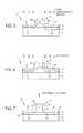
- FIGS. 1-7are schematic, simplified, cross-sectional views illustrating stages in a process for forming a MOS transistor according to an embodiment of the present invention.
- the present inventionis based upon the discovery that formation of high quality, high speed semiconductor devices, e.g., MOS devices such as PMOS transistors, NMOS transistors, and CMOS devices, suitable for use in the manufacture of integrated circuit (IC) devices, can be readily fabricated on or within strained lattice semiconductor materials and substrates by means of a process which substantially eliminates, or at least minimizes, stress relaxation in the strained lattice semiconductor material arising from elevated temperature processing during device fabrication, which stress relaxation disadvantageously mitigates the benefit of increased electron and/or hole mobility, hence operating speed, attributed to the strained lattice.
- MOS devicese.g., MOS devices such as PMOS transistors, NMOS transistors, and CMOS devices
- ICintegrated circuit
- a key feature of the present inventionis performing thermal annealing of amorphized and dopant implanted regions of strained lattice semiconductor materials at temperatures substantially lower than those associated with conventional thermal annealing methodologies, e.g., rapid thermal annealing (RTA), and is based upon recognition by the inventors that such thermal annealing performed at lower-than-conventional RTA temperatures can effect simultaneous recrystallization of the amorphized regions and activation of dopant species implanted therein to reform the regions as source/drain regions of strained lattice semiconductor material having the same amount of lattice strain as the starting material.
- RTArapid thermal annealing
- inventive methodologythe advantages of increased charge carrier mobility, including increased device operating speed, attributable to the use of strained lattice semiconductor material, are retained, i.e., not lost or reduced as a result of lattice stress relaxation arising from thermal processing at elevated temperatures.
- inventive methodologymay be utilized in the manufacture of all manner of semiconductor devices fabricated on or within strained lattice semiconductor substrates, while maintaining full compatibility with all other aspects of process step sequences for the automated manufacture of semiconductor devices such as MOS-based transistors and CMOS devices.
- FIGS. 1-7shown therein are schematic, simplified, cross-sectional views illustrating stages in a process for forming a MOS transistor according to an embodiment of the present invention.
- a substrate/workpiece 1comprising a thin, strained lattice semiconductor layer 2 at an upper surface thereof is provided, which thin, strained lattice semiconductor layer 2 is lattice-matched to a relatively thicker, underlying crystalline semiconductor buffer layer 3 of different composition, the latter being in overlying contact with a suitable substrate 4 .
- the thin, strained lattice semiconductor layer 2comprises a tensilely strained, crystalline Si layer from about 50 to about 200 ⁇ thick, grown on a strain-relaxed, graded composition Si—Ge buffer layer 3 several ⁇ m thick, in turn formed on a suitable substrate 4 , e.g., a crystalline Si wafer or a silicon-on-insulator (SOI) substrate.
- a suitable substrate 4e.g., a crystalline Si wafer or a silicon-on-insulator (SOI) substrate.
- the Si atoms of the strained lattice semiconductor layer 2are deposited on the Si—Ge buffer layer 3 in alignment with the greater lattice constant (spacing) of the Si and Ge atoms therein, relative to pure Si, the deposited Si atoms tend to “stretch” to align with the underlying lattice of Si and Ge atoms, thereby “stretching” or tensilely straining Si layer 2 .
- Typical thicknesses of the graded composition Si—Ge buffer layers 3range from about 500 ⁇ to about 2 ⁇ m.
- Electron and/or hole mobilities in such Si strained lattice semiconductor layers 2 formed on Si—Ge buffer layers 3can be as much as about 70% faster than in conventional, relaxed lattice Si, and transistors and IC devices formed therewith can be up to about 35% faster than equivalent devices formed with conventional Si, without any requirement for size reduction.
- a gate layer stack 5comprised of a thin gate insulator layer 6 , typically a silicon oxide layer less than about 150 ⁇ thick, and a relatively thicker, electrically conductive gate electrode layer 7 , typically a doped polysilicon layer, are formed on a portion of the surface of the Si strained lattice semiconductor layer 2 , as by conventional processing techniques not described herein for brevity.
- shallow implant regions 8 , 8 ′extend for about 10-15 nm below the top surface of strained lattice layer 2 and comprise amorphous Si. formed by implanting ions therein, e.g., Si, Ge, or Xe ions, at implantation energies in the range from about 10 to about 100 KeV.
- substrate/workpiece 1 with shallow pre-amorphized regions 8 , 8 ′ formed thereinis then subjected to a dopant implantation process utilizing the gate layer stack 5 as an implantation mask, to selectively form shallow doped source/drain extension regions 9 , 9 ′ in the exposed regions of the Si strained lattice semiconductor layer 2 , which shallow doped source/drain extension regions 9 , 9 ′ extend beneath respective lateral edges of the gate layer stack 5 and beneath the top surface of layer 2 to a depth just above the interface with the Si—Ge buffer layer 3 (typically 30 nm or less below the surface of the Si strained lattice layer 2 ).
- the dopant speciesmay be n- or p-type, depending upon whether an NMOS or PMOS transistor is to be formed. Implantation may be performed at a dosage of about 10 13 da/cm 2 and suitable dopant species include Sb, As, B, In, or P-containing ions.
- insulative sidewall spacers 9 , 9 ′are formed on the opposite side edges of the gate layer stack 5 , as by conventional blanket insulative layer deposition+anisotropic etching techniques (not described herein in detail for brevity), and the resultant substrate/workpiece 1 is then subjected to a deep post-amorphization implantation process utilizing the gate layer stack 5 +sidewall spacers 10 , 10 ′ as an implantation mask, to selectively form relatively deeper, post-amorphized regions 11 , 11 ′ in the portions of the Si—Ge buffer layer 3 beneath the exposed regions of the Si strained lattice semiconductor layer 2 , for gettering point defects generated during the previous ion implantation process for forming source/drain extension regions 9 , 9 ′ and create vacancies for compensating for interstitials created during dopant implantation, thereby reducing defect density and transient enhanced diffusion (TED) and facilitating formation of ultra-shallow source/d
- TEDdefect density and transient enhanced diffusion
- the post-amorphization regions 11 , 11 ′are amorphous Si—Ge regions formed in substrate/workpiece 1 to extend for a depth into the Si—Ge buffer layer 3 , e.g., by implantation of Si, Ge, or Xe ions of sufficient energy to a depth from about 150 to about 200 nm below the surface of layer 2 .
- the resultant substrate/workpiece 1 with post-amorphization regions 11 , 11 ′ of amorphous Si—Ge formed in the Si—Ge buffer layer 3is then subjected to a deep dopant implantation process utilizing the gate layer stack 5 plus sidewall spacers 10 , 10 ′ as an implantation mask, to selectively form relatively deeper, dopant-implanted source/drain regions 12 , 12 ′ in the portions of the Si—Ge buffer layer 3 beneath the exposed regions of the Si strained lattice semiconductor layer 2 .
- the relatively deeper, dopant-implanted source/drain regions 12 , 12 ′extend for a depth into the Si—Ge buffer layer 3 , and may be formed by, e.g., implantation of 10-100 KeV Sb, As, B, In, or P-containing ions at a dosage of about 1 ⁇ 10 ⁇ 13 to about 1 ⁇ 10 14 da/cm 2 to a depth from about 150 to about 200 nm below the surface of layer 2 .
- the thus-formed substrate/workpiece 1comprising the shallow pre-amorphized regions 7 , 7 ′, shallow dopant-implanted source/drain extension regions 9 , 9 ′, deep post-amorphized regions 11 , 11 ′, and deep dopant-implanted source/drain regions 12 , 12 ′ is subjected to laser thermal annealing (LTA) or rapid thermal annealing (RTA) to reform the shallow pre-amorphized regions 8 , 8 ′ of layer 2 into strained Si by epitaxial re-crystallization with substantially no, or at least minimal, strain relaxation, and to activate the dopants in the shallow source/drain extension regions 9 , 9 ′.
- LTAlaser thermal annealing
- RTArapid thermal annealing
- the deep post-amorphized regions 11 , 11 ′are re-formed by epitaxial re-crystallization and the dopant species in the deep dopant-implanted source/drain regions 12 , 12 ′ are activated.
- thermal annealing of the substrate/workpiece 1is performed at a minimum temperature sufficient to effect epitaxial re-crystallization of the amorphized regions of the Si strained lattice semiconductor layer 2 to re-form a strained lattice semiconductor layer having substantially the original amount of lattice strain (prior to amorphization), whereby strain relaxation of said strained lattice semiconductor arising from said thermal annealing is substantially eliminated or minimized.
- laser thermal annealing (LTA) or rapid thermal annealing (RTA) of the substrate/workpiece of FIG. 7may be performed at a substantially lower-than-conventional temperature from about 500 to about 600° C. for from about 30 sec. to about 5 hrs. to simultaneously re-crystallize and activate implanted dopant species in each of said amorphous regions in said Si strained lattice semiconductor layer and said Si—Ge layer.
- the present inventionthus enables reliable formation of high-quality, high operating speed semiconductor devices based upon strained lattice technology, including MOS transistors and CMOS devices.
- inventive methodologyenjoys utility in the manufacture of numerous other devices requiring enhanced mobility charge carriers.
- the inventioncan be practiced by use of conventional methodologies and instrumentalities at rates consistent with the throughput requirements of automated manufacturing processes and is fully compatible with conventional process flow for the manufacture of high-density integration semiconductor devices.
Landscapes
- Engineering & Computer Science (AREA)
- Physics & Mathematics (AREA)
- Microelectronics & Electronic Packaging (AREA)
- Condensed Matter Physics & Semiconductors (AREA)
- General Physics & Mathematics (AREA)
- Manufacturing & Machinery (AREA)
- Computer Hardware Design (AREA)
- Power Engineering (AREA)
- High Energy & Nuclear Physics (AREA)
- Toxicology (AREA)
- Health & Medical Sciences (AREA)
- Chemical & Material Sciences (AREA)
- Materials Engineering (AREA)
- Crystallography & Structural Chemistry (AREA)
- Insulated Gate Type Field-Effect Transistor (AREA)
Abstract
Description
Claims (12)
Priority Applications (1)
| Application Number | Priority Date | Filing Date | Title |
|---|---|---|---|
| US10/151,946US6689671B1 (en) | 2002-05-22 | 2002-05-22 | Low temperature solid-phase epitaxy fabrication process for MOS devices built on strained semiconductor substrate |
Applications Claiming Priority (1)
| Application Number | Priority Date | Filing Date | Title |
|---|---|---|---|
| US10/151,946US6689671B1 (en) | 2002-05-22 | 2002-05-22 | Low temperature solid-phase epitaxy fabrication process for MOS devices built on strained semiconductor substrate |
Publications (1)
| Publication Number | Publication Date |
|---|---|
| US6689671B1true US6689671B1 (en) | 2004-02-10 |
Family
ID=30769172
Family Applications (1)
| Application Number | Title | Priority Date | Filing Date |
|---|---|---|---|
| US10/151,946Expired - LifetimeUS6689671B1 (en) | 2002-05-22 | 2002-05-22 | Low temperature solid-phase epitaxy fabrication process for MOS devices built on strained semiconductor substrate |
Country Status (1)
| Country | Link |
|---|---|
| US (1) | US6689671B1 (en) |
Cited By (62)
| Publication number | Priority date | Publication date | Assignee | Title |
|---|---|---|---|---|
| US20020084000A1 (en)* | 1997-06-24 | 2002-07-04 | Eugene A. Fitzgerald | Controlling threading dislocation densities in Ge on Si using graded GeSi layers and planarization |
| US20040000691A1 (en)* | 2002-06-28 | 2004-01-01 | Karsten Wieczorek | SOI field effect transistor element having a recombination region and method of forming same |
| US6756276B1 (en)* | 2002-09-30 | 2004-06-29 | Advanced Micro Devices, Inc. | Strained silicon MOSFET having improved source/drain extension dopant diffusion resistance and method for its fabrication |
| US20040175860A1 (en)* | 2003-03-07 | 2004-09-09 | Kwangju Institute Of Science And Technology | Method for manufacturing zinc oxide semiconductors |
| US20040217391A1 (en)* | 2003-04-29 | 2004-11-04 | Micron Technology, Inc. | Localized strained semiconductor on insulator |
| US20040217896A1 (en)* | 2003-01-24 | 2004-11-04 | Stmicroelectronics S.R.L | Multistage analog-to-digital converter |
| US20040221792A1 (en)* | 2003-05-07 | 2004-11-11 | Micron Technology, Inc. | Strained Si/SiGe structures by ion implantation |
| US20040224480A1 (en)* | 2003-05-07 | 2004-11-11 | Micron Technology, Inc. | Micromechanical strained semiconductor by wafer bonding |
| US20040232488A1 (en)* | 2003-05-21 | 2004-11-25 | Micron Technology, Inc. | Silicon oxycarbide substrates for bonded silicon on insulator |
| US20040232487A1 (en)* | 2003-05-21 | 2004-11-25 | Micron Technology, Inc. | Ultra-thin semiconductors bonded on glass substrates |
| US20040232422A1 (en)* | 2003-05-21 | 2004-11-25 | Micron Technology, Inc. | Wafer gettering using relaxed silicon germanium epitaxial proximity layers |
| US6825102B1 (en)* | 2003-09-18 | 2004-11-30 | International Business Machines Corporation | Method of improving the quality of defective semiconductor material |
| US20050020094A1 (en)* | 2003-07-21 | 2005-01-27 | Micron Technology, Inc. | Strained semiconductor by full wafer bonding |
| US6849527B1 (en)* | 2003-10-14 | 2005-02-01 | Advanced Micro Devices | Strained silicon MOSFET having improved carrier mobility, strained silicon CMOS device, and methods of their formation |
| US20050026400A1 (en)* | 2003-06-13 | 2005-02-03 | Todd Michael A. | Methods for depositing amorphous materials and using them as templates for epitaxial films by solid phase epitaxy |
| US20050029619A1 (en)* | 2003-08-05 | 2005-02-10 | Micron Technology, Inc. | Strained Si/SiGe/SOI islands and processes of making same |
| US20050037548A1 (en)* | 2002-06-28 | 2005-02-17 | Advanced Micro Devices, Inc. | SOI field effect transistor element having a recombination region and method of forming same |
| US20050054145A1 (en)* | 2003-09-09 | 2005-03-10 | International Business Machines Corporation | Method for reduced n+ diffusion in strained si on sige substrate |
| US20050112831A1 (en)* | 2003-10-17 | 2005-05-26 | Surdeanu Radu C. | Method and apparatus for forming a semiconductor substrate with a layer structure of activated dopants |
| US6905923B1 (en)* | 2003-07-15 | 2005-06-14 | Advanced Micro Devices, Inc. | Offset spacer process for forming N-type transistors |
| US20050142707A1 (en)* | 2003-12-24 | 2005-06-30 | Kim Yong H. | Method of crystallizing/activating polysilicon layer and method of fabricating thin film transistor having the same polysilicon layer |
| US20050233558A1 (en)* | 2003-06-20 | 2005-10-20 | Fujitsu Limited | Semiconductor device and manufacturing method thereof |
| WO2005064644A3 (en)* | 2003-09-09 | 2005-11-10 | Advanced Micro Devices Inc | Strained silicon mosfets having reduced diffusion of n-type dopants |
| US20060011982A1 (en)* | 2003-03-05 | 2006-01-19 | Micron Technology, Inc. | Micro-mechanically strained semiconductor film |
| US20060014366A1 (en)* | 2002-06-07 | 2006-01-19 | Amberwave Systems Corporation | Control of strain in device layers by prevention of relaxation |
| US20060097281A1 (en)* | 2003-04-29 | 2006-05-11 | Micron Technology, Inc. | Strained semiconductor by wafer bonding with misorientation |
| US7045433B1 (en)* | 2004-04-06 | 2006-05-16 | Advanced Micro Devices, Inc. | Tip architecture with SPE for buffer and deep source/drain regions |
| US20060113568A1 (en)* | 2004-11-30 | 2006-06-01 | International Business Machines Corporation | Structure and method of applying stresses to pfet and nfet transistor channels for improved performance |
| US20060157751A1 (en)* | 2004-12-30 | 2006-07-20 | Soo Cho Y | Metal oxide semiconductor field effect transistor and method of fabricating the same |
| US20060214236A1 (en)* | 2005-03-22 | 2006-09-28 | Chin-Cheng Chien | Semiconductor transistor and method for making the same |
| US20060220112A1 (en)* | 2005-04-01 | 2006-10-05 | International Business Machines Corporation | Semiconductor device forming method and structure for retarding dopant-enhanced diffusion |
| US20060234455A1 (en)* | 2005-04-19 | 2006-10-19 | Chien-Hao Chen | Structures and methods for forming a locally strained transistor |
| US20060258063A1 (en)* | 2003-05-21 | 2006-11-16 | Micron Technology, Inc. | Gettering of silicon on insulator using relaxed silicon germanium epitaxial proximity layers |
| US20070042572A1 (en)* | 2003-07-23 | 2007-02-22 | Matthias Bauer | Deposition of silicon germanium on silicon-on-insulator structures and bulk substrates |
| US20070166960A1 (en)* | 2003-12-16 | 2007-07-19 | Koninklijke Philips Electronic, N.V. | Method for forming a strained si-channel in a mosfet structure |
| US20070173022A1 (en)* | 2006-01-20 | 2007-07-26 | Chih-Hao Wang | Defect-free SiGe source/drain formation by epitaxy-free process |
| US20070281435A1 (en)* | 2006-05-30 | 2007-12-06 | Voon-Yew Thean | Engineering strain in thick strained-soi substrates |
| US20080029840A1 (en)* | 2006-08-02 | 2008-02-07 | Micron Technology, Inc. | Strained semiconductor, devices and systems and methods of formation |
| US20080029832A1 (en)* | 2006-08-03 | 2008-02-07 | Micron Technology, Inc. | Bonded strained semiconductor with a desired surface orientation and conductance direction |
| US20080042211A1 (en)* | 2006-08-18 | 2008-02-21 | Micron Technology, Inc. | Strained semiconductor channels and methods of formation |
| US20080102590A1 (en)* | 2006-10-31 | 2008-05-01 | Andreas Gehring | Method of forming a semiconductor structure comprising a field effect transistor having a stressed channel region |
| WO2008054679A1 (en)* | 2006-10-31 | 2008-05-08 | Advanced Micro Devices, Inc. | Method of forming a semiconductor structure comprising a field effect transistor having a stressed channel region |
| US20080124858A1 (en)* | 2006-08-07 | 2008-05-29 | Bich-Yen Nguyen | Selective stress relaxation by amorphizing implant in strained silicon on insulator integrated circuit |
| US20080171426A1 (en)* | 2007-01-12 | 2008-07-17 | International Business Machines Corporation | Uniaxial strain relaxation of biaxial-strained thin films using ion implantation |
| US20090053865A1 (en)* | 2007-08-20 | 2009-02-26 | Frank Scott Johnson | Method and apparatus for de-interlacing video data |
| CN100477128C (en)* | 2005-07-06 | 2009-04-08 | 台湾积体电路制造股份有限公司 | Methods of Forming Semiconductor Structures |
| US7524740B1 (en) | 2008-04-24 | 2009-04-28 | International Business Machines Corporation | Localized strain relaxation for strained Si directly on insulator |
| US20090108293A1 (en)* | 2007-10-30 | 2009-04-30 | Victor Moroz | Method for Suppressing Lattice Defects in a Semiconductor Substrate |
| US20090298301A1 (en)* | 2003-04-22 | 2009-12-03 | Siegfried Mantl | Method of producing a tensioned layer on a substrate |
| US20100112788A1 (en)* | 2008-10-31 | 2010-05-06 | Deepak Ramappa | Method to reduce surface damage and defects |
| US20110078639A1 (en)* | 2007-10-26 | 2011-03-31 | Synopsys, Inc. | Filler cells for design optimization in a place-and-route system |
| US20110291191A1 (en)* | 2010-01-28 | 2011-12-01 | Shanghai Institute Of Microsystem And Information Technology, Chinese Academy | MOS Structure with Suppressed SOI Floating Body Effect and Manufacturing Method thereof |
| CN101577229B (en)* | 2008-05-06 | 2012-03-28 | 联华电子股份有限公司 | Semiconductor element and manufacturing method thereof |
| US8227309B2 (en) | 2006-02-16 | 2012-07-24 | Micron Technology, Inc. | Localized compressive strained semiconductor |
| US8642434B2 (en) | 2007-01-04 | 2014-02-04 | International Business Machines Corporation | Structure and method for mobility enhanced MOSFETS with unalloyed silicide |
| US20140147981A1 (en)* | 2006-12-08 | 2014-05-29 | Taiwan Semiconductor Manufacturing Company, Ltd. | Inducement of Strain in a Semiconductor Layer |
| US20140242759A1 (en)* | 2010-11-30 | 2014-08-28 | Taiwan Semiconductor Manufacturing Company, Ltd. | Reducing wafer distortion through a high cte layer |
| US20150084130A1 (en)* | 2012-04-28 | 2015-03-26 | Institute of Microelectronics, Chinese Academy of Sciences | Semiconductor structure and method for manufacturing the same |
| US20150145046A1 (en)* | 2012-04-28 | 2015-05-28 | Institute of Microelectronics, Chinese Academy of Sciences | Semiconductor structure and method for manufacturing the same |
| US20150155170A1 (en)* | 2013-11-29 | 2015-06-04 | Commissariat A L'energie Atomique Et Aux Ene Alt | Method of fabricating a semiconductor substrate on insulator |
| US9847229B2 (en)* | 2014-05-09 | 2017-12-19 | Infineon Technologies Ag | Method for forming a semiconductor device and semiconductor device |
| US20190067485A1 (en)* | 2017-08-31 | 2019-02-28 | Semiconductor Manufacturing International (Shanghai) Corporation | Semiconductor structure and fabrication method thereof |
Citations (15)
| Publication number | Priority date | Publication date | Assignee | Title |
|---|---|---|---|---|
| US3269A (en) | 1843-09-14 | Xoltx new new | ||
| US8284A (en) | 1851-08-05 | Bkick-machiwe | ||
| US16383A (en) | 1857-01-13 | Improvement in flour-bolts as | ||
| US24884A (en) | 1859-07-26 | Daxiel morris | ||
| US5565690A (en)* | 1995-02-02 | 1996-10-15 | Motorola, Inc. | Method for doping strained heterojunction semiconductor devices and structure |
| US5759898A (en) | 1993-10-29 | 1998-06-02 | International Business Machines Corporation | Production of substrate for tensilely strained semiconductor |
| US5953615A (en) | 1999-01-27 | 1999-09-14 | Advance Micro Devices | Pre-amorphization process for source/drain junction |
| US6039803A (en) | 1996-06-28 | 2000-03-21 | Massachusetts Institute Of Technology | Utilization of miscut substrates to improve relaxed graded silicon-germanium and germanium layers on silicon |
| US6180476B1 (en) | 1998-11-06 | 2001-01-30 | Advanced Micro Devices, Inc. | Dual amorphization implant process for ultra-shallow drain and source extensions |
| US6180490B1 (en) | 1999-05-25 | 2001-01-30 | Chartered Semiconductor Manufacturing Ltd. | Method of filling shallow trenches |
| US6207530B1 (en) | 1998-06-19 | 2001-03-27 | International Business Machines Corporation | Dual gate FET and process |
| US6214653B1 (en) | 1999-06-04 | 2001-04-10 | International Business Machines Corporation | Method for fabricating complementary metal oxide semiconductor (CMOS) devices on a mixed bulk and silicon-on-insulator (SOI) substrate |
| US6251751B1 (en) | 1997-10-16 | 2001-06-26 | International Business Machines Corporation | Bulk and strained silicon on insulator using local selective oxidation |
| US6300172B1 (en) | 1999-10-01 | 2001-10-09 | Chartered Semiconductor Manufacturing Ltd. | Method of field isolation in silicon-on-insulator technology |
| US6313486B1 (en) | 2000-06-15 | 2001-11-06 | Board Of Regents, The University Of Texas System | Floating gate transistor having buried strained silicon germanium channel layer |
- 2002
- 2002-05-22USUS10/151,946patent/US6689671B1/ennot_activeExpired - Lifetime
Patent Citations (15)
| Publication number | Priority date | Publication date | Assignee | Title |
|---|---|---|---|---|
| US8284A (en) | 1851-08-05 | Bkick-machiwe | ||
| US16383A (en) | 1857-01-13 | Improvement in flour-bolts as | ||
| US24884A (en) | 1859-07-26 | Daxiel morris | ||
| US3269A (en) | 1843-09-14 | Xoltx new new | ||
| US5759898A (en) | 1993-10-29 | 1998-06-02 | International Business Machines Corporation | Production of substrate for tensilely strained semiconductor |
| US5565690A (en)* | 1995-02-02 | 1996-10-15 | Motorola, Inc. | Method for doping strained heterojunction semiconductor devices and structure |
| US6039803A (en) | 1996-06-28 | 2000-03-21 | Massachusetts Institute Of Technology | Utilization of miscut substrates to improve relaxed graded silicon-germanium and germanium layers on silicon |
| US6251751B1 (en) | 1997-10-16 | 2001-06-26 | International Business Machines Corporation | Bulk and strained silicon on insulator using local selective oxidation |
| US6207530B1 (en) | 1998-06-19 | 2001-03-27 | International Business Machines Corporation | Dual gate FET and process |
| US6180476B1 (en) | 1998-11-06 | 2001-01-30 | Advanced Micro Devices, Inc. | Dual amorphization implant process for ultra-shallow drain and source extensions |
| US5953615A (en) | 1999-01-27 | 1999-09-14 | Advance Micro Devices | Pre-amorphization process for source/drain junction |
| US6180490B1 (en) | 1999-05-25 | 2001-01-30 | Chartered Semiconductor Manufacturing Ltd. | Method of filling shallow trenches |
| US6214653B1 (en) | 1999-06-04 | 2001-04-10 | International Business Machines Corporation | Method for fabricating complementary metal oxide semiconductor (CMOS) devices on a mixed bulk and silicon-on-insulator (SOI) substrate |
| US6300172B1 (en) | 1999-10-01 | 2001-10-09 | Chartered Semiconductor Manufacturing Ltd. | Method of field isolation in silicon-on-insulator technology |
| US6313486B1 (en) | 2000-06-15 | 2001-11-06 | Board Of Regents, The University Of Texas System | Floating gate transistor having buried strained silicon germanium channel layer |
Non-Patent Citations (1)
| Title |
|---|
| Yeo et al. "Nanoscale Ulta-thin-body silicon-on-insulator P-MOSFET with a SiGe/Si Heterostructure channel" IEEE Electron Device Letters vol. 21, No. 4, Apr. 2000.* |
Cited By (145)
| Publication number | Priority date | Publication date | Assignee | Title |
|---|---|---|---|---|
| US20020084000A1 (en)* | 1997-06-24 | 2002-07-04 | Eugene A. Fitzgerald | Controlling threading dislocation densities in Ge on Si using graded GeSi layers and planarization |
| US7250359B2 (en)* | 1997-06-24 | 2007-07-31 | Massachusetts Institute Of Technology | Controlling threading dislocation densities in Ge on Si using graded GeSi layers and planarization |
| US7335545B2 (en)* | 2002-06-07 | 2008-02-26 | Amberwave Systems Corporation | Control of strain in device layers by prevention of relaxation |
| US20060014366A1 (en)* | 2002-06-07 | 2006-01-19 | Amberwave Systems Corporation | Control of strain in device layers by prevention of relaxation |
| US6812074B2 (en)* | 2002-06-28 | 2004-11-02 | Advanced Micro Devices, Inc. | SOI field effect transistor element having a recombination region and method of forming same |
| US20050037548A1 (en)* | 2002-06-28 | 2005-02-17 | Advanced Micro Devices, Inc. | SOI field effect transistor element having a recombination region and method of forming same |
| US20040000691A1 (en)* | 2002-06-28 | 2004-01-01 | Karsten Wieczorek | SOI field effect transistor element having a recombination region and method of forming same |
| US7170084B1 (en) | 2002-09-30 | 2007-01-30 | Advanced Micro Devices, Inc. | Strained silicon MOSFET having improved source/drain extension dopant diffusion resistance and method for its fabrication |
| US6756276B1 (en)* | 2002-09-30 | 2004-06-29 | Advanced Micro Devices, Inc. | Strained silicon MOSFET having improved source/drain extension dopant diffusion resistance and method for its fabrication |
| US20040217896A1 (en)* | 2003-01-24 | 2004-11-04 | Stmicroelectronics S.R.L | Multistage analog-to-digital converter |
| US20070164361A1 (en)* | 2003-03-05 | 2007-07-19 | Micron Technology, Inc. | Micro-mechanically strained semiconductor film |
| US7202530B2 (en) | 2003-03-05 | 2007-04-10 | Micron Technology, Inc. | Micro-mechanically strained semiconductor film |
| US7405444B2 (en) | 2003-03-05 | 2008-07-29 | Micron Technology, Inc. | Micro-mechanically strained semiconductor film |
| US20060011982A1 (en)* | 2003-03-05 | 2006-01-19 | Micron Technology, Inc. | Micro-mechanically strained semiconductor film |
| US20040175860A1 (en)* | 2003-03-07 | 2004-09-09 | Kwangju Institute Of Science And Technology | Method for manufacturing zinc oxide semiconductors |
| US6852623B2 (en)* | 2003-03-07 | 2005-02-08 | Kwangju Institute Of Science And Technology | Method for manufacturing zinc oxide semiconductors |
| US20090298301A1 (en)* | 2003-04-22 | 2009-12-03 | Siegfried Mantl | Method of producing a tensioned layer on a substrate |
| US7915148B2 (en)* | 2003-04-22 | 2011-03-29 | Forschungszentrum Julich Gmbh | Method of producing a tensioned layer on a substrate |
| US7023051B2 (en) | 2003-04-29 | 2006-04-04 | Micron Technology, Inc. | Localized strained semiconductor on insulator |
| US7041575B2 (en) | 2003-04-29 | 2006-05-09 | Micron Technology, Inc. | Localized strained semiconductor on insulator |
| US20040217391A1 (en)* | 2003-04-29 | 2004-11-04 | Micron Technology, Inc. | Localized strained semiconductor on insulator |
| US20060097281A1 (en)* | 2003-04-29 | 2006-05-11 | Micron Technology, Inc. | Strained semiconductor by wafer bonding with misorientation |
| US7084429B2 (en) | 2003-04-29 | 2006-08-01 | Micron, Technology, Inc. | Strained semiconductor by wafer bonding with misorientation |
| US20050023616A1 (en)* | 2003-04-29 | 2005-02-03 | Micron Technology, Inc. | Localized strained semiconductor on insulator |
| US7429763B2 (en) | 2003-04-29 | 2008-09-30 | Micron Technology, Inc. | Memory with strained semiconductor by wafer bonding with misorientation |
| US7482190B2 (en) | 2003-05-07 | 2009-01-27 | Micron Technology, Inc. | Micromechanical strained semiconductor by wafer bonding |
| US20050032296A1 (en)* | 2003-05-07 | 2005-02-10 | Micron Technology, Inc. | Micromechanical strained semiconductor by wafer bonding |
| US20040221792A1 (en)* | 2003-05-07 | 2004-11-11 | Micron Technology, Inc. | Strained Si/SiGe structures by ion implantation |
| US20040224480A1 (en)* | 2003-05-07 | 2004-11-11 | Micron Technology, Inc. | Micromechanical strained semiconductor by wafer bonding |
| US20050285139A1 (en)* | 2003-05-07 | 2005-12-29 | Micron Technology, Inc. | Strained Si/SiGe structures by ion implantation |
| US7045874B2 (en) | 2003-05-07 | 2006-05-16 | Micron Technology, Inc. | Micromechanical strained semiconductor by wafer bonding |
| US6987037B2 (en)* | 2003-05-07 | 2006-01-17 | Micron Technology, Inc. | Strained Si/SiGe structures by ion implantation |
| US7394111B2 (en) | 2003-05-07 | 2008-07-01 | Micron Technology, Inc. | Strained Si/SiGe structures by ion implantation |
| US7273788B2 (en) | 2003-05-21 | 2007-09-25 | Micron Technology, Inc. | Ultra-thin semiconductors bonded on glass substrates |
| US20060001094A1 (en)* | 2003-05-21 | 2006-01-05 | Micron Technology, Inc. | Semiconductor on insulator structure |
| US7501329B2 (en) | 2003-05-21 | 2009-03-10 | Micron Technology, Inc. | Wafer gettering using relaxed silicon germanium epitaxial proximity layers |
| US20060263994A1 (en)* | 2003-05-21 | 2006-11-23 | Micron Technology, Inc. | Semiconductors bonded on glass substrates |
| US20040232488A1 (en)* | 2003-05-21 | 2004-11-25 | Micron Technology, Inc. | Silicon oxycarbide substrates for bonded silicon on insulator |
| US20060258063A1 (en)* | 2003-05-21 | 2006-11-16 | Micron Technology, Inc. | Gettering of silicon on insulator using relaxed silicon germanium epitaxial proximity layers |
| US7687329B2 (en) | 2003-05-21 | 2010-03-30 | Micron Technology, Inc. | Gettering of silicon on insulator using relaxed silicon germanium epitaxial proximity layers |
| US7008854B2 (en) | 2003-05-21 | 2006-03-07 | Micron Technology, Inc. | Silicon oxycarbide substrates for bonded silicon on insulator |
| US7662701B2 (en) | 2003-05-21 | 2010-02-16 | Micron Technology, Inc. | Gettering of silicon on insulator using relaxed silicon germanium epitaxial proximity layers |
| US7504310B2 (en) | 2003-05-21 | 2009-03-17 | Micron Technology, Inc. | Semiconductors bonded on glass substrates |
| US7271445B2 (en) | 2003-05-21 | 2007-09-18 | Micron Technology, Inc. | Ultra-thin semiconductors bonded on glass substrates |
| US20040232487A1 (en)* | 2003-05-21 | 2004-11-25 | Micron Technology, Inc. | Ultra-thin semiconductors bonded on glass substrates |
| US20040232422A1 (en)* | 2003-05-21 | 2004-11-25 | Micron Technology, Inc. | Wafer gettering using relaxed silicon germanium epitaxial proximity layers |
| US7528463B2 (en) | 2003-05-21 | 2009-05-05 | Micron Technolgy, Inc. | Semiconductor on insulator structure |
| US20050026400A1 (en)* | 2003-06-13 | 2005-02-03 | Todd Michael A. | Methods for depositing amorphous materials and using them as templates for epitaxial films by solid phase epitaxy |
| US7029995B2 (en) | 2003-06-13 | 2006-04-18 | Asm America, Inc. | Methods for depositing amorphous materials and using them as templates for epitaxial films by solid phase epitaxy |
| US8084338B2 (en)* | 2003-06-20 | 2011-12-27 | Fujitsu Semiconductor Limited | Semiconductor device and manufacturing method thereof |
| US20050233558A1 (en)* | 2003-06-20 | 2005-10-20 | Fujitsu Limited | Semiconductor device and manufacturing method thereof |
| US6905923B1 (en)* | 2003-07-15 | 2005-06-14 | Advanced Micro Devices, Inc. | Offset spacer process for forming N-type transistors |
| US7439158B2 (en) | 2003-07-21 | 2008-10-21 | Micron Technology, Inc. | Strained semiconductor by full wafer bonding |
| US7989311B2 (en) | 2003-07-21 | 2011-08-02 | Micron Technlogy, Inc. | Strained semiconductor by full wafer bonding |
| US7994595B2 (en) | 2003-07-21 | 2011-08-09 | Micron Technology, Inc. | Strained semiconductor by full wafer bonding |
| US20050020094A1 (en)* | 2003-07-21 | 2005-01-27 | Micron Technology, Inc. | Strained semiconductor by full wafer bonding |
| US8470687B2 (en) | 2003-07-21 | 2013-06-25 | Micron Technology, Inc. | Strained semiconductor by full wafer bonding |
| US20090042360A1 (en)* | 2003-07-21 | 2009-02-12 | Micron Technology Inc. | Strained semiconductor by full wafer bonding |
| US20070042572A1 (en)* | 2003-07-23 | 2007-02-22 | Matthias Bauer | Deposition of silicon germanium on silicon-on-insulator structures and bulk substrates |
| US20050087842A1 (en)* | 2003-08-05 | 2005-04-28 | Micron Technology, Inc. | Strained Si/SiGe/SOI islands and processes of making same |
| US7153753B2 (en) | 2003-08-05 | 2006-12-26 | Micron Technology, Inc. | Strained Si/SiGe/SOI islands and processes of making same |
| US20050029619A1 (en)* | 2003-08-05 | 2005-02-10 | Micron Technology, Inc. | Strained Si/SiGe/SOI islands and processes of making same |
| US7262428B2 (en) | 2003-08-05 | 2007-08-28 | Micron Technology, Inc. | Strained Si/SiGe/SOI islands and processes of making same |
| US7297601B2 (en) | 2003-09-09 | 2007-11-20 | International Business Machines Corporation | Method for reduced N+ diffusion in strained Si on SiGe substrate |
| WO2005064644A3 (en)* | 2003-09-09 | 2005-11-10 | Advanced Micro Devices Inc | Strained silicon mosfets having reduced diffusion of n-type dopants |
| US7410846B2 (en)* | 2003-09-09 | 2008-08-12 | International Business Machines Corporation | Method for reduced N+ diffusion in strained Si on SiGe substrate |
| US20050145992A1 (en)* | 2003-09-09 | 2005-07-07 | Dureseti Chidambarrao | Method for reduced N+ diffusion in strained Si on SiGe substrate |
| US20050054145A1 (en)* | 2003-09-09 | 2005-03-10 | International Business Machines Corporation | Method for reduced n+ diffusion in strained si on sige substrate |
| US7345329B2 (en) | 2003-09-09 | 2008-03-18 | International Business Machines Corporation | Method for reduced N+ diffusion in strained Si on SiGe substrate |
| US6825102B1 (en)* | 2003-09-18 | 2004-11-30 | International Business Machines Corporation | Method of improving the quality of defective semiconductor material |
| US6849527B1 (en)* | 2003-10-14 | 2005-02-01 | Advanced Micro Devices | Strained silicon MOSFET having improved carrier mobility, strained silicon CMOS device, and methods of their formation |
| US7214592B2 (en)* | 2003-10-17 | 2007-05-08 | Interuniversitair Microelektronica Centrum (Imec) | Method and apparatus for forming a semiconductor substrate with a layer structure of activated dopants |
| US20070267660A1 (en)* | 2003-10-17 | 2007-11-22 | Interuniversitair Microelektronica Centrum (Imec) | Method and apparatus for forming a semiconductor substrate with a layer structure of activated dopants |
| US20050112831A1 (en)* | 2003-10-17 | 2005-05-26 | Surdeanu Radu C. | Method and apparatus for forming a semiconductor substrate with a layer structure of activated dopants |
| US7416957B2 (en)* | 2003-12-16 | 2008-08-26 | Nxp B.V. | Method for forming a strained Si-channel in a MOSFET structure |
| US20070166960A1 (en)* | 2003-12-16 | 2007-07-19 | Koninklijke Philips Electronic, N.V. | Method for forming a strained si-channel in a mosfet structure |
| US20050142707A1 (en)* | 2003-12-24 | 2005-06-30 | Kim Yong H. | Method of crystallizing/activating polysilicon layer and method of fabricating thin film transistor having the same polysilicon layer |
| US7517740B2 (en)* | 2003-12-24 | 2009-04-14 | Electronics And Telecommunications Research Institute | Method of crystallizing/activating polysilicon layer and method of fabricating thin film transistor having the same polysilicon layer |
| US7045433B1 (en)* | 2004-04-06 | 2006-05-16 | Advanced Micro Devices, Inc. | Tip architecture with SPE for buffer and deep source/drain regions |
| US20060113568A1 (en)* | 2004-11-30 | 2006-06-01 | International Business Machines Corporation | Structure and method of applying stresses to pfet and nfet transistor channels for improved performance |
| US7193254B2 (en) | 2004-11-30 | 2007-03-20 | International Business Machines Corporation | Structure and method of applying stresses to PFET and NFET transistor channels for improved performance |
| US7432541B2 (en)* | 2004-12-30 | 2008-10-07 | Dongbuanam Semiconductor Inc. | Metal oxide semiconductor field effect transistor |
| US7622356B2 (en) | 2004-12-30 | 2009-11-24 | Dongbu Electronics Co., Ltd. | Method of fabricating metal oxide semiconductor field effect transistor |
| US20080318386A1 (en)* | 2004-12-30 | 2008-12-25 | Dongbu Electronics Co., Ltd. | Metal oxide semiconductor field effect transistor and method of fabricating the same |
| US20060157751A1 (en)* | 2004-12-30 | 2006-07-20 | Soo Cho Y | Metal oxide semiconductor field effect transistor and method of fabricating the same |
| US20070254439A1 (en)* | 2005-03-22 | 2007-11-01 | Chin-Cheng Chien | Method for making semiconductor transistor |
| US7545023B2 (en)* | 2005-03-22 | 2009-06-09 | United Microelectronics Corp. | Semiconductor transistor |
| US20060214236A1 (en)* | 2005-03-22 | 2006-09-28 | Chin-Cheng Chien | Semiconductor transistor and method for making the same |
| US20060220112A1 (en)* | 2005-04-01 | 2006-10-05 | International Business Machines Corporation | Semiconductor device forming method and structure for retarding dopant-enhanced diffusion |
| US20060234455A1 (en)* | 2005-04-19 | 2006-10-19 | Chien-Hao Chen | Structures and methods for forming a locally strained transistor |
| CN100477128C (en)* | 2005-07-06 | 2009-04-08 | 台湾积体电路制造股份有限公司 | Methods of Forming Semiconductor Structures |
| US20070173022A1 (en)* | 2006-01-20 | 2007-07-26 | Chih-Hao Wang | Defect-free SiGe source/drain formation by epitaxy-free process |
| US8900980B2 (en) | 2006-01-20 | 2014-12-02 | Taiwan Semiconductor Manufacturing Company, Ltd. | Defect-free SiGe source/drain formation by epitaxy-free process |
| US9899519B2 (en) | 2006-01-20 | 2018-02-20 | Taiwan Semiconductor Manufacturing Company, Ltd. | Defect-Free SiGe source/drain formation by epitaxy-free process |
| US8227309B2 (en) | 2006-02-16 | 2012-07-24 | Micron Technology, Inc. | Localized compressive strained semiconductor |
| US8435850B2 (en) | 2006-02-16 | 2013-05-07 | Micron Technology, Inc. | Localized compressive strained semiconductor |
| US7468313B2 (en) | 2006-05-30 | 2008-12-23 | Freescale Semiconductor, Inc. | Engineering strain in thick strained-SOI substrates |
| US20070281435A1 (en)* | 2006-05-30 | 2007-12-06 | Voon-Yew Thean | Engineering strain in thick strained-soi substrates |
| US7888744B2 (en) | 2006-08-02 | 2011-02-15 | Micron Technology, Inc. | Strained semiconductor, devices and systems and methods of formation |
| US7485544B2 (en) | 2006-08-02 | 2009-02-03 | Micron Technology, Inc. | Strained semiconductor, devices and systems and methods of formation |
| US20090108363A1 (en)* | 2006-08-02 | 2009-04-30 | Leonard Forbes | Strained semiconductor, devices and systems and methods of formation |
| US20080029840A1 (en)* | 2006-08-02 | 2008-02-07 | Micron Technology, Inc. | Strained semiconductor, devices and systems and methods of formation |
| US8962447B2 (en) | 2006-08-03 | 2015-02-24 | Micron Technology, Inc. | Bonded strained semiconductor with a desired surface orientation and conductance direction |
| US20080029832A1 (en)* | 2006-08-03 | 2008-02-07 | Micron Technology, Inc. | Bonded strained semiconductor with a desired surface orientation and conductance direction |
| US20080124858A1 (en)* | 2006-08-07 | 2008-05-29 | Bich-Yen Nguyen | Selective stress relaxation by amorphizing implant in strained silicon on insulator integrated circuit |
| US9379241B2 (en) | 2006-08-18 | 2016-06-28 | Micron Technology, Inc. | Semiconductor device with strained channels |
| US20080042211A1 (en)* | 2006-08-18 | 2008-02-21 | Micron Technology, Inc. | Strained semiconductor channels and methods of formation |
| US7968960B2 (en) | 2006-08-18 | 2011-06-28 | Micron Technology, Inc. | Methods of forming strained semiconductor channels |
| US20080102590A1 (en)* | 2006-10-31 | 2008-05-01 | Andreas Gehring | Method of forming a semiconductor structure comprising a field effect transistor having a stressed channel region |
| WO2008054679A1 (en)* | 2006-10-31 | 2008-05-08 | Advanced Micro Devices, Inc. | Method of forming a semiconductor structure comprising a field effect transistor having a stressed channel region |
| US7772077B2 (en) | 2006-10-31 | 2010-08-10 | Advanced Micro Devices, Inc. | Method of forming a semiconductor structure comprising a field effect transistor having a stressed channel region |
| GB2456712B (en)* | 2006-10-31 | 2011-08-17 | Advanced Micro Devices Inc | Method of forming a semiconductor structure comprising a field effect transistor having a stressed channel region |
| GB2456712A (en)* | 2006-10-31 | 2009-07-29 | Advanced Micro Devices Inc | Method of forming a semiconductor structure comprising a field effect transistor having a stressed channel region |
| KR101365714B1 (en)* | 2006-10-31 | 2014-02-21 | 어드밴스드 마이크로 디바이시즈, 인코포레이티드 | Method of forming a semiconductor structure comprising a field effect transistor having a stressed channel region |
| US9484434B2 (en)* | 2006-12-08 | 2016-11-01 | Taiwan Semiconductor Manufacturing Company, Ltd. | Inducement of strain in a semiconductor layer |
| US20140147981A1 (en)* | 2006-12-08 | 2014-05-29 | Taiwan Semiconductor Manufacturing Company, Ltd. | Inducement of Strain in a Semiconductor Layer |
| US8642434B2 (en) | 2007-01-04 | 2014-02-04 | International Business Machines Corporation | Structure and method for mobility enhanced MOSFETS with unalloyed silicide |
| US9059316B2 (en) | 2007-01-04 | 2015-06-16 | International Business Machines Corporation | Structure and method for mobility enhanced MOSFETs with unalloyed silicide |
| US20080171426A1 (en)* | 2007-01-12 | 2008-07-17 | International Business Machines Corporation | Uniaxial strain relaxation of biaxial-strained thin films using ion implantation |
| US7494886B2 (en)* | 2007-01-12 | 2009-02-24 | International Business Machines Corporation | Uniaxial strain relaxation of biaxial-strained thin films using ion implantation |
| US20090053865A1 (en)* | 2007-08-20 | 2009-02-26 | Frank Scott Johnson | Method and apparatus for de-interlacing video data |
| WO2009026350A3 (en)* | 2007-08-20 | 2009-04-30 | Texas Instruments Inc | Semiconductor device source and drain regions formed utilizing dual capping layers and split thermal processes |
| US7785970B2 (en) | 2007-08-20 | 2010-08-31 | Texas Instruments Incorporated | Method of forming source and drain regions utilizing dual capping layers and split thermal processes |
| US20110078639A1 (en)* | 2007-10-26 | 2011-03-31 | Synopsys, Inc. | Filler cells for design optimization in a place-and-route system |
| US8504969B2 (en) | 2007-10-26 | 2013-08-06 | Synopsys, Inc. | Filler cells for design optimization in a place-and-route system |
| JP2011501437A (en)* | 2007-10-30 | 2011-01-06 | シノプシス, インコーポレイテッド | Method for suppressing lattice defects in semiconductor substrates |
| US9472423B2 (en)* | 2007-10-30 | 2016-10-18 | Synopsys, Inc. | Method for suppressing lattice defects in a semiconductor substrate |
| US20090108293A1 (en)* | 2007-10-30 | 2009-04-30 | Victor Moroz | Method for Suppressing Lattice Defects in a Semiconductor Substrate |
| US20100025777A1 (en)* | 2007-10-30 | 2010-02-04 | Synopsys, Inc. | Method for suppressing lattice defects in a semiconductor substrate |
| US7524740B1 (en) | 2008-04-24 | 2009-04-28 | International Business Machines Corporation | Localized strain relaxation for strained Si directly on insulator |
| CN101577229B (en)* | 2008-05-06 | 2012-03-28 | 联华电子股份有限公司 | Semiconductor element and manufacturing method thereof |
| US20100112788A1 (en)* | 2008-10-31 | 2010-05-06 | Deepak Ramappa | Method to reduce surface damage and defects |
| US20110291191A1 (en)* | 2010-01-28 | 2011-12-01 | Shanghai Institute Of Microsystem And Information Technology, Chinese Academy | MOS Structure with Suppressed SOI Floating Body Effect and Manufacturing Method thereof |
| US20140242759A1 (en)* | 2010-11-30 | 2014-08-28 | Taiwan Semiconductor Manufacturing Company, Ltd. | Reducing wafer distortion through a high cte layer |
| US9153435B2 (en)* | 2010-11-30 | 2015-10-06 | Taiwan Semiconductor Manufacturing Company, Ltd. | Reducing wafer distortion through a high CTE layer |
| US20150145046A1 (en)* | 2012-04-28 | 2015-05-28 | Institute of Microelectronics, Chinese Academy of Sciences | Semiconductor structure and method for manufacturing the same |
| US9548317B2 (en)* | 2012-04-28 | 2017-01-17 | Institute of Microelectronics, Chinese Academy of Sciences | FDSOI semiconductor structure and method for manufacturing the same |
| US20150084130A1 (en)* | 2012-04-28 | 2015-03-26 | Institute of Microelectronics, Chinese Academy of Sciences | Semiconductor structure and method for manufacturing the same |
| US20150155170A1 (en)* | 2013-11-29 | 2015-06-04 | Commissariat A L'energie Atomique Et Aux Ene Alt | Method of fabricating a semiconductor substrate on insulator |
| US9899217B2 (en)* | 2013-11-29 | 2018-02-20 | Commissariat A L'energie Atomique Et Aux Energies Alternatives | Method for producing a strained semiconductor on insulator substrate |
| US9847229B2 (en)* | 2014-05-09 | 2017-12-19 | Infineon Technologies Ag | Method for forming a semiconductor device and semiconductor device |
| US20190067485A1 (en)* | 2017-08-31 | 2019-02-28 | Semiconductor Manufacturing International (Shanghai) Corporation | Semiconductor structure and fabrication method thereof |
| CN109427681A (en)* | 2017-08-31 | 2019-03-05 | 中芯国际集成电路制造(上海)有限公司 | Semiconductor structure and forming method thereof |
| CN109427681B (en)* | 2017-08-31 | 2020-12-22 | 中芯国际集成电路制造(上海)有限公司 | Semiconductor structure and method of forming the same |
| US11038063B2 (en)* | 2017-08-31 | 2021-06-15 | Semiconductor Manufacturing International (Shanghai) Corporation | Semiconductor structure and fabrication method thereof |
Similar Documents
| Publication | Publication Date | Title |
|---|---|---|
| US6689671B1 (en) | Low temperature solid-phase epitaxy fabrication process for MOS devices built on strained semiconductor substrate | |
| US8067805B2 (en) | Ultra shallow junction formation by epitaxial interface limited diffusion | |
| KR100414736B1 (en) | A method for forming a transistor of a semiconductor device | |
| US7217627B2 (en) | Semiconductor devices having diffusion barrier regions and halo implant regions and methods of fabricating the same | |
| CN101523608B (en) | N-channel mosfets comprising dual stressors, and methods for forming the same | |
| US6638802B1 (en) | Forming strained source drain junction field effect transistors | |
| US7867851B2 (en) | Methods of forming field effect transistors on substrates | |
| US20040173815A1 (en) | Strained-channel transistor structure with lattice-mismatched zone | |
| US6403433B1 (en) | Source/drain doping technique for ultra-thin-body SOI MOS transistors | |
| US20090087971A1 (en) | Method for fabricating semiconductor devices with reduced junction diffusion | |
| US6180476B1 (en) | Dual amorphization implant process for ultra-shallow drain and source extensions | |
| US7550336B2 (en) | Method for fabricating an NMOS transistor | |
| US20070184600A1 (en) | Stressed-channel CMOS transistors | |
| US20060088969A1 (en) | Solid phase epitaxy recrystallization by laser annealing | |
| JPH11168069A (en) | Method for manufacturing semiconductor device | |
| JPH06310719A (en) | Ge-Si SOI MOS transistor and method of manufacturing the same | |
| US6808970B2 (en) | Semiconductor device having an improved strained surface layer and method of forming a strained surface layer in a semiconductor device | |
| US8653604B1 (en) | Multiple transistor types formed in a common epitaxial layer by differential out-diffusion from a doped underlayer | |
| US8173503B2 (en) | Fabrication of source/drain extensions with ultra-shallow junctions | |
| US6809016B1 (en) | Diffusion stop implants to suppress as punch-through in SiGe | |
| US20080009111A1 (en) | Manufacturing method of semiconductor device | |
| US6727136B1 (en) | Formation of ultra-shallow depth source/drain extensions for MOS transistors | |
| US6630386B1 (en) | CMOS manufacturing process with self-amorphized source/drain junctions and extensions | |
| US6905923B1 (en) | Offset spacer process for forming N-type transistors | |
| US6423601B1 (en) | Retrograde well structure formation by nitrogen implantation |
Legal Events
| Date | Code | Title | Description |
|---|---|---|---|
| AS | Assignment | Owner name:ADVANCED MICRO DEVICES, INC., CALIFORNIA Free format text:ASSIGNMENT OF ASSIGNORS INTEREST;ASSIGNORS:YU, BIN;WRISTERS, DERICK J.;REEL/FRAME:012923/0265;SIGNING DATES FROM 20020419 TO 20020425 | |
| STCF | Information on status: patent grant | Free format text:PATENTED CASE | |
| FPAY | Fee payment | Year of fee payment:4 | |
| AS | Assignment | Owner name:GLOBALFOUNDRIES INC., CAYMAN ISLANDS Free format text:AFFIRMATION OF PATENT ASSIGNMENT;ASSIGNOR:ADVANCED MICRO DEVICES, INC.;REEL/FRAME:023119/0083 Effective date:20090630 | |
| FPAY | Fee payment | Year of fee payment:8 | |
| FPAY | Fee payment | Year of fee payment:12 | |
| AS | Assignment | Owner name:WILMINGTON TRUST, NATIONAL ASSOCIATION, DELAWARE Free format text:SECURITY AGREEMENT;ASSIGNOR:GLOBALFOUNDRIES INC.;REEL/FRAME:049490/0001 Effective date:20181127 | |
| AS | Assignment | Owner name:GLOBALFOUNDRIES U.S. INC., CALIFORNIA Free format text:ASSIGNMENT OF ASSIGNORS INTEREST;ASSIGNOR:GLOBALFOUNDRIES INC.;REEL/FRAME:054633/0001 Effective date:20201022 | |
| AS | Assignment | Owner name:GLOBALFOUNDRIES INC., CAYMAN ISLANDS Free format text:RELEASE BY SECURED PARTY;ASSIGNOR:WILMINGTON TRUST, NATIONAL ASSOCIATION;REEL/FRAME:054636/0001 Effective date:20201117 | |
| AS | Assignment | Owner name:GLOBALFOUNDRIES U.S. INC., NEW YORK Free format text:RELEASE BY SECURED PARTY;ASSIGNOR:WILMINGTON TRUST, NATIONAL ASSOCIATION;REEL/FRAME:056987/0001 Effective date:20201117 |