US6689660B1 - 4 F2 folded bit line DRAM cell structure having buried bit and word lines - Google Patents
4 F2 folded bit line DRAM cell structure having buried bit and word linesDownload PDFInfo
- Publication number
- US6689660B1 US6689660B1US09/527,981US52798100AUS6689660B1US 6689660 B1US6689660 B1US 6689660B1US 52798100 AUS52798100 AUS 52798100AUS 6689660 B1US6689660 B1US 6689660B1
- Authority
- US
- United States
- Prior art keywords
- forming
- layer
- transistors
- vertical transistors
- trenches
- Prior art date
- Legal status (The legal status is an assumption and is not a legal conclusion. Google has not performed a legal analysis and makes no representation as to the accuracy of the status listed.)
- Expired - Lifetime
Links
- 230000015654memoryEffects0.000claimsabstractdescription125
- 238000000034methodMethods0.000claimsabstractdescription76
- 229910052710siliconInorganic materials0.000claimsabstractdescription47
- 239000010703siliconSubstances0.000claimsabstractdescription47
- 230000008569processEffects0.000claimsabstractdescription20
- 238000002955isolationMethods0.000claimsabstractdescription18
- 239000012212insulatorSubstances0.000claimsabstractdescription11
- 239000000758substrateSubstances0.000claimsdescription61
- XUIMIQQOPSSXEZ-UHFFFAOYSA-NSiliconChemical compound[Si]XUIMIQQOPSSXEZ-UHFFFAOYSA-N0.000claimsdescription57
- 239000000463materialSubstances0.000claimsdescription51
- 239000004065semiconductorSubstances0.000claimsdescription47
- 239000003990capacitorSubstances0.000claimsdescription17
- 238000003860storageMethods0.000claimsdescription15
- 229910021420polycrystalline siliconInorganic materials0.000claimsdescription14
- 229920005591polysiliconPolymers0.000claimsdescription14
- 239000004020conductorSubstances0.000claimsdescription13
- 239000003989dielectric materialSubstances0.000claimsdescription10
- 230000006870functionEffects0.000claimsdescription8
- 238000004519manufacturing processMethods0.000claimsdescription5
- 230000001590oxidative effectEffects0.000claimsdescription5
- 239000002210silicon-based materialSubstances0.000claimsdescription5
- 238000000151depositionMethods0.000claimsdescription4
- 238000005530etchingMethods0.000claimsdescription4
- 125000006850spacer groupChemical group0.000claimsdescription3
- VYPSYNLAJGMNEJ-UHFFFAOYSA-NSilicium dioxideChemical compoundO=[Si]=OVYPSYNLAJGMNEJ-UHFFFAOYSA-N0.000description41
- 239000000377silicon dioxideSubstances0.000description16
- 229910052681coesiteInorganic materials0.000description14
- 229910052906cristobaliteInorganic materials0.000description14
- 229910052682stishoviteInorganic materials0.000description14
- 229910052905tridymiteInorganic materials0.000description14
- 229910052581Si3N4Inorganic materials0.000description10
- 238000005229chemical vapour depositionMethods0.000description6
- 238000005516engineering processMethods0.000description5
- KRHYYFGTRYWZRS-UHFFFAOYSA-NFluoraneChemical compoundFKRHYYFGTRYWZRS-UHFFFAOYSA-N0.000description4
- 230000003647oxidationEffects0.000description4
- 238000007254oxidation reactionMethods0.000description4
- 229920002120photoresistant polymerPolymers0.000description4
- 230000015572biosynthetic processEffects0.000description3
- 239000000872bufferSubstances0.000description3
- 239000000126substanceSubstances0.000description3
- 230000005669field effectEffects0.000description2
- 239000011159matrix materialSubstances0.000description2
- QPJSUIGXIBEQAC-UHFFFAOYSA-Nn-(2,4-dichloro-5-propan-2-yloxyphenyl)acetamideChemical compoundCC(C)OC1=CC(NC(C)=O)=C(Cl)C=C1ClQPJSUIGXIBEQAC-UHFFFAOYSA-N0.000description2
- 230000009467reductionEffects0.000description2
- 235000012239silicon dioxideNutrition0.000description2
- HQVNEWCFYHHQES-UHFFFAOYSA-Nsilicon nitrideChemical compoundN12[Si]34N5[Si]62N3[Si]51N64HQVNEWCFYHHQES-UHFFFAOYSA-N0.000description2
- QTBSBXVTEAMEQO-UHFFFAOYSA-NAcetic acidChemical groupCC(O)=OQTBSBXVTEAMEQO-UHFFFAOYSA-N0.000description1
- GRYLNZFGIOXLOG-UHFFFAOYSA-NNitric acidChemical compoundO[N+]([O-])=OGRYLNZFGIOXLOG-UHFFFAOYSA-N0.000description1
- 230000004913activationEffects0.000description1
- 230000015556catabolic processEffects0.000description1
- 230000000295complement effectEffects0.000description1
- 238000007796conventional methodMethods0.000description1
- 230000007423decreaseEffects0.000description1
- 238000006731degradation reactionMethods0.000description1
- 230000036039immunityEffects0.000description1
- 238000002513implantationMethods0.000description1
- 238000005468ion implantationMethods0.000description1
- 150000002500ionsChemical class0.000description1
- 239000002184metalSubstances0.000description1
- 239000000203mixtureSubstances0.000description1
- 229910021421monocrystalline siliconInorganic materials0.000description1
- 229910017604nitric acidInorganic materials0.000description1
- 239000002245particleSubstances0.000description1
- 238000005498polishingMethods0.000description1
- 230000004044responseEffects0.000description1
- 238000005549size reductionMethods0.000description1
- 230000003068static effectEffects0.000description1
- 230000001360synchronised effectEffects0.000description1
- 238000012876topographyMethods0.000description1
Images


Classifications
- H—ELECTRICITY
- H10—SEMICONDUCTOR DEVICES; ELECTRIC SOLID-STATE DEVICES NOT OTHERWISE PROVIDED FOR
- H10B—ELECTRONIC MEMORY DEVICES
- H10B12/00—Dynamic random access memory [DRAM] devices
- H10B12/01—Manufacture or treatment
- H10B12/02—Manufacture or treatment for one transistor one-capacitor [1T-1C] memory cells
- H10B12/05—Making the transistor
- H10B12/053—Making the transistor the transistor being at least partially in a trench in the substrate
- H—ELECTRICITY
- H10—SEMICONDUCTOR DEVICES; ELECTRIC SOLID-STATE DEVICES NOT OTHERWISE PROVIDED FOR
- H10B—ELECTRONIC MEMORY DEVICES
- H10B12/00—Dynamic random access memory [DRAM] devices
- H10B12/30—DRAM devices comprising one-transistor - one-capacitor [1T-1C] memory cells
- H10B12/34—DRAM devices comprising one-transistor - one-capacitor [1T-1C] memory cells the transistor being at least partially in a trench in the substrate
Definitions
- the present inventionrelates generally to semiconductor memory devices, and in particular, the present invention relates to a folded bit line memory cell structure including buried bit and word lines for a dynamic random access memory device.
- DRAMsdynamic random access memories
- FETfield-effect transistor
- capacitorwhich functions as a storage element.
- VLSIvery large scale integrated
- DRAMdynamic random access memory
- Cell structures used through the 256 Megabit generationhave been fundamentally limited to a size of at least 8 F 2 , where F is a minimum lithographic feature size.
- This size limitationis imposed by the wiring requirements of passing both an active and passing word lines through the cell to achieve the low noise benefits of folded bit line architecture. This limitation can be removed by either relinquishing the folded bit line architecture or by devising a sub lithographic wiring technique.
- a further limitationis imposed by the area required to form the source region, the drain region and the channel region of the FET array device on a planar surface.
- Another limitationis imposed by the area that is required for fabricating the storage capacitor which, in a stacked capacitor technology, must compete with the bit line and word line wiring for space above the silicon surface.
- a memory cell structure for a semiconductor memory devicesuch as dynamic random access memory device, which employs a folded bit line architecture and in which the surface area of the memory cells is minimized, providing a memory cell structure that is less than 8 F 2 in size, resulting in increased density for the memory device.
- the present inventionprovides a memory array cell structure for a semiconductor memory device.
- the memory arrayincludes buried bit and word lines, and access transistors are formed as vertical structures on the bit lines. Isolation trenches extend orthogonally to the bit lines between the access transistors of adjacent memory cells. First and second word lines, which are located in each of the isolation trenches, are adapted to gate alternate ones of the access transistors located adjacent to the trench, allowing both an active and a passing word line to be contained within each memory cell, thereby providing a folded bit line architecture for the memory array.
- the width of the access transistorsis determined by the width F of the bit lines, where F is a minimum feature size.
- each memory cell of the memory arrayhas a surface area that is approximately 4 F 2 while maintaining a folded bit line architecture.
- the memory cell structure provided by the inventionresults in a high density semiconductor memory array having an improved topography and which achieves the low noise benefits of a folded bit line architecture.
- a method for producing a memory array including a plurality of memory cells on a semiconductor substrateincludes the steps of providing a semiconductor substrate and forming a plurality of layers of semiconducting material on a surface of the substrate, including a first layer of a material of a first conductivity type formed on the substrate, a second layer of a material of a second conductivity type formed on the first layer, and a third layer of a material of the first conductivity type formed on the second layer.
- a plurality of first trenchesare formed in the layers of semiconducting material to form a plurality of bars having the first, second and third layers of semiconducting material, with the first layer of semiconducting material of each of the bars functioning as a bit line for the memory array.
- a plurality of second trenchesare formed in the stack of layers of semiconducting material in a direction that is orthogonal to the direction of the bit lines to define a plurality of in-line access transistors on each of the bit lines, with each of the access transistors having a vertical channel region, defined by the second layer of material, exposed in a sidewall of one of the second trenches.
- a gate oxideis formed on a sidewall of the trench, overlying the channel regions of each of the access transistors.
- first and second word linesare formed in each of the second trenches, with the first word line extending in the proximity of the channel regions of the access transistors on first alternate ones of the bit lines; and with the second word line extending in the proximity of the channel regions of the access transistors on second alternate ones of the bit lines.
- the second trenchesare filled with a dielectric material to bury the first and second word lines in the dielectric material in the second trenches.
- the methodcan be carried out using either bulk silicon or silicon on insulator processing techniques.
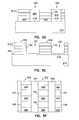
- FIG. 1is a representation of a semiconductor memory device including a matrix of the memory cells provided by the invention
- FIG. 2is a perspective view of a portion of a semiconductor memory device provided by the invention and produced using a bulk silicon processing technique, and illustrating a plurality of the memory cells of the memory device;
- FIG. 3is a plan view of the memory device portion of FIG. 2;
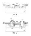
- FIG. 4is a section view taken along the line 4 — 4 of FIG. 3;
- FIGS. 5A-5Millustrate steps in the process of forming the semiconductor memory device in accordance with the invention
- FIG. 6is a perspective view of a portion of a semiconductor memory device provided by the invention and which is produced using a silicon on insulator process, and illustrating a plurality of the memory cells of the memory device;
- FIG. 7is a vertical section view taken along the line 7 — 7 of FIG. 6;
- FIGS. 8A-8Cillustrate steps relating to a silicon on insulator process used in fabricating the semiconductor memory device of FIG. 6 .
- wafer and substrate used in the following descriptioninclude any semiconductor-based structure having an exposed silicon surface in which to form the integrated circuit structure of the invention. Wafer and substrate are used interchangeably to refer to semiconductor structures during processing.
- FIG. 1is a representation of a semiconductor memory device 100 incorporating the memory cells provided by the invention.
- the semiconductor memory device 100is a dynamic random access memory (DRAM).
- DRAMdynamic random access memory
- the inventioncan be applied to other semiconductor memory devices, such as static random access memory devices, synchronous random access memory devices or other types of memory devices that include a matrix of memory cells that are selected or addressed by selectively activation of row and column conductors.
- the basic memory device 100is well known in the art to include a memory array 110 constructed of rows and columns of memory cells 112 having inputs and outputs corresponding to rows and columns.
- the array 110has N rows and N columns with complementary, paired bit lines BL 0 , BL 0 * . . . BLn, BLn*, and word (address) lines WL 0 , WL 1 . . . WLn.
- bit line pairs BL 0 , BL 0 * . . . BLn, BLn*are used to write information into the memory cells 112 and to read data from the memory cells.
- the word lines WL 0 -WLnare used to address or select the memory cell to which data is to be written or read.
- Address buffer circuits 114control row decoders 116 , and column decoders of column decoder and input/output circuitry 118 to access the memory cells 112 of the memory array 110 in response to address signals AO-AN that are provided on address lines 120 during write and read operations.
- Sense amplifiers 124are connected to each bit line pair.
- Data provided on data input/outputs 122is written into the memory, and data read from the memory is applied to the data input/outputs 122 .
- the address signalsare provided by an external controller (not shown), such as a standard microprocessor. All of the memory cells 112 of the memory array 110 are identical, and accordingly, only one memory cell is described herein.
- Each memory cell 112includes an n-channel field-effect transistor 130 and a storage capacitor 132 .
- the n-channel transistor 130has a source-to-drain circuit connected to a bit line BL, which represents any one of the bit lines BL 0 , BL 1 . . . BLn, BLn, shown in FIG. 1, and a gate electrode connected to a word line WL, which represents any one of the word lines WL 0 -WLn shown in FIG. 1 .
- memory device 100receives an address of a selected memory cell at address buffers 114 .
- Address buffers 114identify one of the word lines WL 0 -WLn of a selected memory cell to the row decoder 116 .
- the row decoder 116activates the selected word line to activate the access transistors 130 of each cells connected to the selected word line.
- the column decoders of column decoder and input/output circuitry 118select the particular memory cell indicated by the address.
- data provided on the data input/outputs 122causes the storage capacitor 132 of the selected cell to be charged, or to be maintained discharged, to represent the data.
- the data stored in the selected cellis transferred to the data input/outputs 122 .
- FIG. 2is a perspective view of a portion of a DRAM device provided in accordance with one embodiment of the invention, and illustrates two memory cells, indicated by reference numerals 112 a and 112 b , and the transistors 130 for two other memory cells, indicated by reference numerals 112 c and 112 d , along with segments of a bitline pair 202 , 204 , which can be any one of the bitline pairs BL 0 , BL 0 * . . . BLn, BLn* and segments of word lines 206 , 207 and 208 , which can be any of the word lines WL 0 -WLn.
- FIG. 3is a plan view of the portion of the memory device shown in FIG. 2, and FIG. 4 is a vertical section view taken along the line 4 — 4 of FIG. 3 .
- the memory deviceis fabricated on a substrate 210 using bulk silicon processing techniques.
- the transistor 130 of each memory cellis formed as a vertical device including a layer of n+ material 212 formed on substrate 210 , a layer of p ⁇ material 214 formed on the layer of n-type material 212 , and a further layer of n+ material 216 formed on the layer of p ⁇ material 214 .
- the n+ layer 212forms one of the source/drain regions of the transistor 130 and functions as the bit line for the memory cell.
- the n+ layer 216forms the other one of the source/drain regions of the transistor 130 .
- the p ⁇ layer 214 of the vertically oriented transistor 130functions as the body portion of the transistor and defines the channel portion of the transistor 130 .
- a gate oxide layer 218which is formed on the sidewall of transistor structure, overlies the channel portion of the transistor 130 on one side of the transistor 130 .
- the active devices or transistors 130 of the memory cellsare isolated from one another by isolation trenches 220 , 221 and 222 that are filled with a dielectric material, such as silicon dioxide 224 (not shown in FIG. 2 ).
- the trenches 220extend in the bit line direction for isolating the transistors 130 of the memory cells on adjacent bit lines, such as the transistors 130 of memory cells 112 a and 112 c , and the transistors 130 of memory cells 112 b and 112 d .
- the trench 221extends orthogonal to the trench 220 , and to the bit lines 202 and 204 , defining the transistors 130 of in-line pairs of the memory cells, such as transistors 130 of the memory cell pair 112 a and 112 b , and transistors 130 of the memory cell pair 112 c and 112 d .
- trench 222defines the transistors of in-line memory cells 112 b and 112 d and the transistors of further memory cells (not shown).
- the gate oxide 218is grown on a sidewall 219 of the trench 221 at which one side of the transistor structure is exposed during fabrication of the memory cell.
- the body portion 214 of each of the semiconductor devices that forms one of the transistors of the memory cellsis floating and is fully depleted.
- the cell transistors 130 for the memory cells 112are formed on the bit line.
- Each of the bit linessuch as bit lines 202 and 204 , consists of a single crystal silicon bar upon which a row of separate memory cells is formed.
- memory cells 112 a and 112 bare formed on a portion of bit line 202
- memory cells 112 c and 112 dare formed on a portion of bit line 204 .
- the bit linesare fabricated to be in contact with the silicon substrate 210 as is shown in FIGS. 2 and 4, for example.
- the word linessuch as word lines 206 and 207 , which gate the transistors 130 , are located in the isolation channel or trench 221 between memory cells, spaced apart from one another by the dielectric material 224 , such as SiO 2 .
- the word linesare oriented vertically widthwise in the trench.
- the word linescan be formed of an n+ polysilicon or a suitable metal.
- Two word lines, such as word lines 206 and 207are formed within a single trench 221 that extends between the memory cells 112 a - 112 d . As shown in FIG.
- both an active word line, defined by word line portion 228 of word line 206 , and a passing word line, defined by passing word line portion 229 of word line 207 ,can be contained within each cell to provide folded bit line architecture.
- Each word linegates the transistors of alternate in-line memory devices.
- the word line 206is positioned to be spaced apart from the vertical sidewall 219 of the transistor 130 of memory cell 112 c by a layer 225 of SiO 2 that is formed together with layer 224 of SiO 2
- Word line 206includes ajog that defines active word line portion 228 adjacent to the transistor 130 of memory cell 112 a that the word line 206 gates, so that the word line 206 contacts the gate oxide 218 formed on the sidewall 219 .
- the other word line 207 that is located within the trench 221is spaced apart from the transistor 130 of memory cell 112 b by oxide 224 and includes ajog 228 so that the word line 207 engages the gate oxide 218 of the transistor 130 of the memory cell 112 d that the word line 207 gates.
- word line 206gates the access transistor 130 of memory cell 112 a and is isolated by dielectric material 224 from the access transistor 130 of memory cell 112 c .
- Word line 207is isolated from the access transistor 130 of memory cell 112 b and gates the access transistor 130 of memory cell 112 d .
- the access transistor of memory cell 112 bis gated by word line 208 which is isolated from the access transistor of memory cell 112 d
- the access transistor of memory cell 112 cis gated by a further word line (not shown) that extends in a trench along the opposite sidewall of the transistor.
- the width of the cell transistor 130corresponds to the width of the bit line, or one feature size “F” and the length to the cell transistor is approximately “F”.
- the word linesare oriented vertically widthwise, with both active and passing word lines contained in each memory cell to provide a folded bit line architecture.
- the surface area of each memory cellis approximately “4F 2 ”, while preserving the folded bit line architecture.
- Word line wiringis achieved on a half “F” (0.5F) pitch by using the sidewall spaced defined conductors which gate alternate cell devices.
- all of the bit lines BL 0 , BL 0 * . . . BLn, BLn* and all of the word lines WL 0 . . . WLnare fabricated to be located beneath the surface of the silicon.
- the bit line pair 202 , 204 and the word lines 206 , 207 and 208are located beneath the active silicon surface 230 . This frees up space on the upper portion of the memory device for formation of the capacitor of the memory cell on the upper portion of the memory cell, thus maximizing the possible storage area that is available for a given cell area.
- Contacts to the bit lines and to the word linescan be made outside of the memory array by using conventional methods of contact hole etching and stud formation.
- a stacked capacitorsuch as the capacitors 132 illustrated for memory devices 112 a and 112 b , is formed on the top of the vertical device pillar using any of the many capacitor structures and process sequences known in the art.
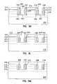
- FIGS. 5A-5MOne process for fabricating the memory cells 112 is described with reference to FIGS. 5A-5M.
- the memory cells 112are produced using bulk silicon processing techniques.
- the dimensionsare appropriate to a 0.2 ⁇ m CD technology and can be scaled accordingly for other CD sizes.
- certain of the elements that correspond to elements of the memory cells 112 of FIGS. 2-4have been given the same reference numerals in FIGS. 5A-5M.
- a layer 212 of n+ materialis formed on the substrate 210 by ion implantation or epitaxial growth.
- the thickness of the layer 212is that of the desired bit line thickness which is typically in the range of 0.2 to 0.5 ⁇ m.
- An epitaxial layer 214 of p ⁇ siliconis grown to contain the device channel.
- the thickness of the layer 214 of p ⁇ materialcan be in the order of 0.4 ⁇ m.
- the upper layer 216 of n+ materialis formed by implantation or epitaxial growth.
- a pad layer 510is formed by depositing a thin layer 512 of SiO 2 on the upper layer 216 n+ material.
- the SiO 2 layer 512can be 10 nm in thickness.
- a layer 514 of silicon nitride Si 3 N 4is deposited on the SiO 2 layer 512 using techniques well known in the art, such as chemical vapor deposition (CVD).
- the thickness of the layer 514 of Si 3 N 4can be 100 nm.
- photo resistis applied and masked to expose rows or bars 516 containing the stacked layers of n+ material 212 , p ⁇ material 214 and n+ material 216 , with the bars 516 being oriented in the bit line direction.
- the pad 510 and the siliconare directionally etched to form the trenches 220 as shown in FIG. 5 C.
- the exposed pad and silicon regionscan be etched away with a directional etchant, preferably a reactive ion etch (RIE), to form trenches in the substrate.
- RIEreactive ion etch
- the silicon barscan have a width of one micron or less and preferably corresponds to the minimum feature size F.
- the trench widthcan be approximately equal to the width of the silicon bars.
- SiO 2 material 224is deposited to fill the trenches 220 , providing the structure shown in FIG. 5 D.
- the surfaceis planarized using a conventional planarization method, such as chemical mechanical polishing (CMP).
- FIGS. 5E and 5Fare views of the semiconductor structure rotated clockwise ninety degrees relative to FIG. 5D, then, a photo resist material is applied and masked to expose bars 532 , that are formed using a directional etch, preferably RIE, in a direction that is orthogonal to the bit line direction and which define the transistors 130 .
- the adjacent access transistors in each of the rowsi.e., the transistors on adjacent bit lines, being separated from one another by the oxide filled trenches 220 .
- the orthogonal relationship between the oxide filled trenches 220 and trenches 221 , 222is shown in FIG. 5F, for example, which is a plan view of the portion of the memory device.
- the exposed SiO 2 and siliconare etched into the bar 204 , that functions as the bit line, to a depth of about 100 nm as is shown in FIG. 5E, forming a plurality of pillars 538 , shown in FIG. 5G, each of the pillars including stacked layers of n+ material 212 , p ⁇ material 214 , and n+ material 216 that define the access transistor 130 for one of the memory cells 112 .
- a conformal layer 540 of silicon nitride Si 3 N 4is deposited and directionally etched to leave the Si 3 N 4 only on the sidewalls 219 of the pillars 538 that define the transistors 130 .
- the thickness of the layer 540 of Si 3 N 4is about 20 nm.
- a layer 542 of thermal oxide SiO 2is grown on the base of the trenches 221 and 222 to insulate the exposed bit line bars.
- the thickness of the layer of SiO 2is about 100 nm. After the layer of SiO 2 has been grown, the thin layer of Si 3 N 4 is stripped.
- intrinsic polysiliconis deposited using CVD to a thickness of about 50 nm, providing the structure shown in FIG. 5 H.
- the layer 544 of polysiliconis etched directionally to leave polysilicon on only the vertical sidewalls of the pillars 538 .
- photo resistis applied and masked to expose the sidewall 219 of each pillar on which the device channels are to be formed, and a gate oxide 218 is grown on the exposed sidewall of the pillar, providing the structure shown in FIG. 5 I.
- the gate oxidealso is grown on the remaining intrinsic polysilicon.
- n+ polysilicon or other suitable conductoris CVD deposited to a thickness of approximately 60 nm, to form the word line conductors 206 , 207 , 208 and 209 .
- the polysiliconis directionally etched, forming the pattern shown in FIG. 3, leaving the polysilicon that forms the active portion 228 (FIG. 3) of the word line conductor 207 only on the gate oxide 218 that overlies the vertical sidewall of the access transistor for memory cell 112 d , and active portion 228 of word line conductor 208 , exposed in the trenches 221 and 222 , and leaving the polysilicon that forms the passive portions 229 (FIG. 3) of the word line conductors 206 and 207 only on the intrinsic polysilicon 544 , providing the structure shown in FIG. 5 J.
- a brief oxide etchis performed to expose the top portion of the intrinsic polysilicon. Then, an isotropic etch is carried out to remove all of the remaining intrinsic polysilicon, forming a cavity 550 between each word line and the sidewall that is adjacent to the word line as is shown in FIG. 5 K.
- the word linessuch as word lines 206 and 207 that extend within trench 221 , are spaced apart from one another forming a gap 552 therebetween.
- an anisotropic etchis carried out to recess the top of the word lines, such as word lines 206 and 207 , to below the approximate level of the silicon surface, which is defined by the interface between layer 512 of SiO 2 and the upper layer 216 n+ silicon material.
- a dielectric materialsuch as SiO 2 , indicated by reference numeral 224 , is CVD deposited to fill in the cavities 550 that are created as the result of removal of the intrinsic polysilicon and to fill the spaces 552 between the word line conductors, providing the structure shown in FIG. 5 L.
- the surfaceis planarized down to the Si 3 N 4 layer 514 using CMP or any other suitable planarization process.
- the remaining Si 3 N 4 layer 514is removed using an etching process.
- a layer 224 of SiO 2is CVD deposited to cover the active surface of the substrate, providing the structure shown in FIG. 5 M.
- the structure thus formedis then processed using known techniques to fabricate a storage capacitor on the upper surface of the structure, followed by conventional back end of line (BEOL) procedures.
- BEOLback end of line
- FIGS. 6 and 7there is shown a portion of a DRAM device provided in accordance with a second embodiment of the invention.
- the DRAM deviceincludes memory cells 112 a - 112 d that are similar to those for DRAM device shown in FIGS. 2-4. Accordingly, elements of the memory cells of the DRAM device shown in FIG. 6 have been given the same reference number as like elements of the memory cells of DRAM device shown in FIG. 2 .
- the memory cellsare fabricated using a silicon on insulator (SOI) process. This provides a layer 602 of silicon dioxide Si 0 2 that isolates the bit lines, such as the bit lines 202 and 204 , and the transistors 130 formed thereon, from the substrate 210 .
- SOIsilicon on insulator
- the process for fabricating the memory cells for the DRAM deviceis similar to that described above with reference to FIGS. 5A-5M for fabricating the memory cells for the DRAM device shown in FIGS. 2-4, except for the formation of the isolation layer 602 between the substrate and the active devices of the memory cells.
- the isolation layer between the substrate and the active devices of the memory cellscan be produced using the procedure described in the U.S. patent application, Ser. No. 08/706,230 of Leonard Forbes, which is entitled “Technique For Producing Small Islands of Silicon on Insulator” and which is assigned to Micron Technology, Inc. This patent application is incorporated herein by reference.
- n material 212 , p ⁇ material 214 and n material 216are formed on the substrate 210 , as described above with reference to FIGS. 5A-5C, and the trenches 220 are formed, defining the silicon bars 516 on which the transistors 130 are defined in subsequent process steps.
- the depth of the etchis to the full SOI depth, which is below the surface 802 of the substrate and which is greater than or approximately equal to 0.6 ⁇ m, providing the structure shown in FIG. 8 A.
- an isotropic chemical etchis used to partially undercut the bars 516 of silicon, as shown in FIG. 8B.
- a standard chemical etch using hydrofluoric acid (HF) or a commercial etchant sold under the trade name CP4 (a mixture of approximately 1 part (46% HF): 1 t (CH 3 COOH):3 parts (HNO3))is used for the isotropic etchant. It is important to use an isotropic etch for this step to compensate for the volume of oxide to be formed in the next step. In general, the volume of oxide formed is approximately twice that of the silicon 210 consumed.
- the substrate 210is then oxidized using a standard silicon processing furnace at a temperature of approximately 900 to 1,100 degrees Celsius, providing the structure shown in FIG. 8C which includes an oxide layer 602 isolating the bit lines and the active devices formed on the bit lines from the substrate 210 .
- a wet, oxidizing ambientis used in the furnace chamber to oxidize the exposed silicon regions on the lower part of the trenches in a parallel direction to the surface of the substrate 210 .
- the substrate 210is oxidized for a time period, such that oxide fully undercuts the bottom of the silicon rows, leaving isolated silicon rows. By using narrow, sub-micron rows of silicon and appropriately designed process conditions, generally planar structures are formed. The larger volume of oxide fills the trenches between the rows.
- the time period for oxidationdepends on the width of the rows and the effective width after the undercut step. As the desired size of the silicon rows decreases, so does the required oxidation time. For example, for sub-0.25 micron technology, oxidation time is approximately 1 hour.
- Undercutting the silicon rowsreduces the effective width of the rows to a distance small enough that a relatively short, simple oxidation can fully undercut the silicon rows. Fully undercutting the rows of silicon is possible because the width of the rows is one micron or less.
- the processthen continues with the steps described above with reference to FIGS. 5D-5M, to fill the trenches 220 with oxide 224 , to produce the trenches 221 and 222 , and to form the word line conductors 206 - 209 in the trenches 221 and 222 , providing the structure shown in FIGS. 6-7.
- the inventionprovides a memory cell structure for a DRAM memory device.
- the memory cell structureincludes a vertical transistor fabricated on the bit line for the memory cell.
- the word line conductorsare buried in the oxide contained in an isolation trench that extends between the access transistors for the memory cell. Forming the access transistors on the bit lines of the memory array, with the feature size of the access transistors defined by the bit lines, and with the vertical orientation and 0.5F pitch of the word lines of the memory array, allows the surface area of each of the memory cells to be approximately 4F 2 .
- each isolation trenchcontains both an active word line and a passing word line to provide folded bit line architecture for the memory array.
- Each word linegates the transistors of alternate in-line memory devices.
- the memory cell structurecan be formed using a bulk silicon process or by using silicon on insulator techniques.
Landscapes
- Engineering & Computer Science (AREA)
- Manufacturing & Machinery (AREA)
- Semiconductor Memories (AREA)
Abstract
Description
Claims (41)
Priority Applications (1)
| Application Number | Priority Date | Filing Date | Title |
|---|---|---|---|
| US09/527,981US6689660B1 (en) | 1997-07-08 | 2000-03-17 | 4 F2 folded bit line DRAM cell structure having buried bit and word lines |
Applications Claiming Priority (2)
| Application Number | Priority Date | Filing Date | Title |
|---|---|---|---|
| US08/889,463US6072209A (en) | 1997-07-08 | 1997-07-08 | Four F2 folded bit line DRAM cell structure having buried bit and word lines |
| US09/527,981US6689660B1 (en) | 1997-07-08 | 2000-03-17 | 4 F2 folded bit line DRAM cell structure having buried bit and word lines |
Related Parent Applications (1)
| Application Number | Title | Priority Date | Filing Date |
|---|---|---|---|
| US08/889,463DivisionUS6072209A (en) | 1997-07-08 | 1997-07-08 | Four F2 folded bit line DRAM cell structure having buried bit and word lines |
Publications (1)
| Publication Number | Publication Date |
|---|---|
| US6689660B1true US6689660B1 (en) | 2004-02-10 |
Family
ID=25395152
Family Applications (3)
| Application Number | Title | Priority Date | Filing Date |
|---|---|---|---|
| US08/889,463Expired - LifetimeUS6072209A (en) | 1997-07-08 | 1997-07-08 | Four F2 folded bit line DRAM cell structure having buried bit and word lines |
| US09/527,981Expired - LifetimeUS6689660B1 (en) | 1997-07-08 | 2000-03-17 | 4 F2 folded bit line DRAM cell structure having buried bit and word lines |
| US09/571,352Expired - LifetimeUS6476434B1 (en) | 1997-07-08 | 2000-05-16 | 4 F2 folded bit line dram cell structure having buried bit and word lines |
Family Applications Before (1)
| Application Number | Title | Priority Date | Filing Date |
|---|---|---|---|
| US08/889,463Expired - LifetimeUS6072209A (en) | 1997-07-08 | 1997-07-08 | Four F2 folded bit line DRAM cell structure having buried bit and word lines |
Family Applications After (1)
| Application Number | Title | Priority Date | Filing Date |
|---|---|---|---|
| US09/571,352Expired - LifetimeUS6476434B1 (en) | 1997-07-08 | 2000-05-16 | 4 F2 folded bit line dram cell structure having buried bit and word lines |
Country Status (1)
| Country | Link |
|---|---|
| US (3) | US6072209A (en) |
Cited By (233)
| Publication number | Priority date | Publication date | Assignee | Title |
|---|---|---|---|---|
| US20030008461A1 (en)* | 2001-02-09 | 2003-01-09 | Micron Technology, Inc. | Flash memory with ultra thin vertical body transistors |
| US20030045078A1 (en)* | 2001-08-30 | 2003-03-06 | Micron Technology, Inc. | Highly reliable amorphous high-K gate oxide ZrO2 |
| US20030107402A1 (en)* | 2001-02-09 | 2003-06-12 | Micron Technology, Inc. | Programmable logic arrays with ultra thin body transistors |
| US20030218199A1 (en)* | 2001-02-09 | 2003-11-27 | Micron Technology, Inc. | Open bit line DRAM with ultra-thin body transistors |
| US20040007721A1 (en)* | 2001-02-09 | 2004-01-15 | Micron Technology, Inc. | Folded bit line DRAM with vertical ultra thin body transistors |
| US20040032773A1 (en)* | 2001-02-09 | 2004-02-19 | Micron Technology, Inc. | Programmable memory address and decode circuits with vertical body transistors |
| US20050026349A1 (en)* | 2001-08-30 | 2005-02-03 | Micron Technology, Inc. | Flash memory with low tunnel barrier interpoly insulators |
| US20060046522A1 (en)* | 2004-08-31 | 2006-03-02 | Micron Technology, Inc. | Atomic layer deposited lanthanum aluminum oxide dielectric layer |
| US20060043473A1 (en)* | 2004-09-01 | 2006-03-02 | Eppich Anton P | Memory cell, array, device and system with overlapping buried digit line and active area and method for forming same |
| US20060043492A1 (en)* | 2004-08-26 | 2006-03-02 | Micron Technology, Inc. | Ruthenium gate for a lanthanide oxide dielectric layer |
| US20060125030A1 (en)* | 2004-12-13 | 2006-06-15 | Micron Technology, Inc. | Hybrid ALD-CVD of PrxOy/ZrO2 films as gate dielectrics |
| US20060172483A1 (en)* | 2005-02-03 | 2006-08-03 | Micron Technology, Inc. | DRAM arrays, vertical transistor structures and methods of forming transistor structures and DRAM arrays |
| US20060177975A1 (en)* | 2005-02-10 | 2006-08-10 | Micron Technology, Inc. | Atomic layer deposition of CeO2/Al2O3 films as gate dielectrics |
| KR100660881B1 (en) | 2005-10-12 | 2006-12-26 | 삼성전자주식회사 | Semiconductor device with vertical channel transistor and manufacturing method thereof |
| US20070048926A1 (en)* | 2005-08-31 | 2007-03-01 | Micron Technology, Inc. | Lanthanum aluminum oxynitride dielectric films |
| US20070048940A1 (en)* | 2005-07-18 | 2007-03-01 | Saifun Semiconductors Ltd. | Dense non-volatile memory array and method of fabrication |
| US20070049054A1 (en)* | 2005-08-31 | 2007-03-01 | Micron Technology, Inc. | Cobalt titanium oxide dielectric films |
| US20070105357A1 (en)* | 2005-09-01 | 2007-05-10 | Micron Technology, Inc. | Silicided recessed silicon |
| US20070101929A1 (en)* | 2002-05-02 | 2007-05-10 | Micron Technology, Inc. | Methods for atomic-layer deposition |
| US20070120180A1 (en)* | 2005-11-25 | 2007-05-31 | Boaz Eitan | Transition areas for dense memory arrays |
| US20070178643A1 (en)* | 2002-07-08 | 2007-08-02 | Micron Technology, Inc. | Memory utilizing oxide-conductor nanolaminates |
| KR100800469B1 (en) | 2005-10-05 | 2008-02-01 | 삼성전자주식회사 | Circuit device and manufacturing method comprising vertical transistor connected to buried bit line |
| US20080048333A1 (en)* | 2006-08-24 | 2008-02-28 | Samsung Electronics Co., Ltd. | Semiconductor Device Having Buried Word Line Interconnects and Method of Fabricating the Same |
| US7405454B2 (en) | 2003-03-04 | 2008-07-29 | Micron Technology, Inc. | Electronic apparatus with deposited dielectric layers |
| US20080258204A1 (en)* | 2007-04-20 | 2008-10-23 | Macronix International Co., Ltd. | Memory structure and operating method thereof |
| US20080299753A1 (en)* | 2005-09-01 | 2008-12-04 | Figura Thomas A | Peripheral Gate Stacks and Recessed Array Gates |
| US7560793B2 (en) | 2002-05-02 | 2009-07-14 | Micron Technology, Inc. | Atomic layer deposition and conversion |
| US20090206400A1 (en)* | 2008-02-19 | 2009-08-20 | Micron Technology, Inc. | Systems and devices including fin transistors and methods of using, making, and operating the same |
| US20090206443A1 (en)* | 2008-02-19 | 2009-08-20 | Micron Technology, Inc. | Devices including fin transistors robust to gate shorts and methods of making the same |
| US20090207681A1 (en)* | 2008-02-19 | 2009-08-20 | Micron Technology, Inc. | Systems and devices including local data lines and methods of using, making, and operating the same |
| US20090224357A1 (en)* | 2008-03-06 | 2009-09-10 | Micron Technology, Inc. | Devices with cavity-defined gates and methods of making the same |
| US20090237996A1 (en)* | 2008-03-20 | 2009-09-24 | Micron Technology, Inc. | Memory structure having volatile and non-volatile memory portions |
| US20090238010A1 (en)* | 2008-03-20 | 2009-09-24 | Micron Technology, Inc. | Systems and devices including multi-transistor cells and methods of using, making, and operating the same |
| US20090238000A1 (en)* | 2008-03-20 | 2009-09-24 | Micron Technology, Inc. | Systems and devices including multi-gate transistors and methods of using, making, and operating the same |
| US20090251946A1 (en)* | 2008-04-03 | 2009-10-08 | Micron Technology, Inc. | Data cells with drivers and methods of making and operating the same |
| US20090261415A1 (en)* | 2008-04-17 | 2009-10-22 | Adkisson James W | Fully-depleted low-body doping field effect transistor (fet) with reverse short channel effects (sce) induced by self-aligned edge back-gate(s) |
| US20090294842A1 (en)* | 2008-05-30 | 2009-12-03 | Micron Technology, Inc. | Methods of forming data cells and connections to data cells |
| US20090303794A1 (en)* | 2008-06-04 | 2009-12-10 | Macronix International Co., Ltd. | Structure and Method of A Field-Enhanced Charge Trapping-DRAM |
| US7662729B2 (en) | 2005-04-28 | 2010-02-16 | Micron Technology, Inc. | Atomic layer deposition of a ruthenium layer to a lanthanide oxide dielectric layer |
| US7709402B2 (en) | 2006-02-16 | 2010-05-04 | Micron Technology, Inc. | Conductive layers for hafnium silicon oxynitride films |
| US7728626B2 (en) | 2002-07-08 | 2010-06-01 | Micron Technology, Inc. | Memory utilizing oxide nanolaminates |
| US20100148249A1 (en)* | 2005-09-01 | 2010-06-17 | Micron Technology, Inc. | Method Of Manufacturing A Memory Device |
| US20100173464A1 (en)* | 2004-10-14 | 2010-07-08 | Eli Lusky | Non-volatile memory structure and method of fabrication |
| US20100173727A1 (en)* | 2007-07-03 | 2010-07-08 | Sullivan Michael J | Golf ball having reduced surface hardness |
| US20100173460A1 (en)* | 2005-06-13 | 2010-07-08 | Micron Technology, Inc. | Vertical transistor, memory cell, device, system and method of forming same |
| US20100276748A1 (en)* | 2007-06-28 | 2010-11-04 | Ahn Kie Y | Method of forming lutetium and lanthanum dielectric structures |
| CN101369582B (en)* | 2007-08-15 | 2011-03-30 | 旺宏电子股份有限公司 | Vertical non-volatile memory and manufacturing method thereof |
| US20110081757A1 (en)* | 2007-01-22 | 2011-04-07 | Werner Juengling | Memory having a vertical access device |
| US20110101448A1 (en)* | 2009-10-30 | 2011-05-05 | Inotera Memories, Inc. | Vertical transistor and manufacturing method thereof |
| WO2011062605A1 (en)* | 2009-11-17 | 2011-05-26 | Magic Technologies, Inc. | Method of high density field induced mram process |
| US8148776B2 (en) | 2008-09-15 | 2012-04-03 | Micron Technology, Inc. | Transistor with a passive gate |
| US20120104491A1 (en)* | 2010-11-01 | 2012-05-03 | Lars Heineck | Memory Cells, Arrays Of Memory Cells, And Methods Of Forming Memory Cells |
| US8254173B2 (en) | 2010-08-31 | 2012-08-28 | Micron Technology, Inc. | NAND memory constructions |
| US8329567B2 (en) | 2010-11-03 | 2012-12-11 | Micron Technology, Inc. | Methods of forming doped regions in semiconductor substrates |
| US20130001674A1 (en)* | 2011-06-30 | 2013-01-03 | Infineon Technologies Austria Ag | Semiconductor device with voltage compensation structure |
| US8450175B2 (en) | 2011-02-22 | 2013-05-28 | Micron Technology, Inc. | Methods of forming a vertical transistor and at least a conductive line electrically coupled therewith |
| US8501563B2 (en) | 2005-07-20 | 2013-08-06 | Micron Technology, Inc. | Devices with nanocrystals and methods of formation |
| US8569831B2 (en) | 2011-05-27 | 2013-10-29 | Micron Technology, Inc. | Integrated circuit arrays and semiconductor constructions |
| US8716116B2 (en) | 2010-03-10 | 2014-05-06 | Micron Technology, Inc. | Method of forming a DRAM array of devices with vertically integrated recessed access device and digitline |
| US8810310B2 (en) | 2010-11-19 | 2014-08-19 | Micron Technology, Inc. | Vertically stacked fin transistors and methods of fabricating and operating the same |
| US9006060B2 (en) | 2012-08-21 | 2015-04-14 | Micron Technology, Inc. | N-type field effect transistors, arrays comprising N-type vertically-oriented transistors, methods of forming an N-type field effect transistor, and methods of forming an array comprising vertically-oriented N-type transistors |
| US9036391B2 (en) | 2012-03-06 | 2015-05-19 | Micron Technology, Inc. | Arrays of vertically-oriented transistors, memory arrays including vertically-oriented transistors, and memory cells |
| US9111853B2 (en) | 2013-03-15 | 2015-08-18 | Micron Technology, Inc. | Methods of forming doped elements of semiconductor device structures |
| US9129896B2 (en) | 2012-08-21 | 2015-09-08 | Micron Technology, Inc. | Arrays comprising vertically-oriented transistors, integrated circuitry comprising a conductive line buried in silicon-comprising semiconductor material, methods of forming a plurality of conductive lines buried in silicon-comprising semiconductor material, and methods of forming an array comprising vertically-oriented transistors |
| US9166005B2 (en) | 2013-03-01 | 2015-10-20 | Infineon Technologies Austria Ag | Semiconductor device with charge compensation structure |
| US9478550B2 (en) | 2012-08-27 | 2016-10-25 | Micron Technology, Inc. | Arrays of vertically-oriented transistors, and memory arrays including vertically-oriented transistors |
| US20180047707A1 (en)* | 2012-12-22 | 2018-02-15 | Monolithic 3D Inc. | 3d semiconductor device and structure |
| US20180254286A1 (en)* | 2000-08-14 | 2018-09-06 | Sandisk Technologies Llc | Dense arrays and charge storage devices |
| US10127344B2 (en) | 2013-04-15 | 2018-11-13 | Monolithic 3D Inc. | Automation for monolithic 3D devices |
| US10224279B2 (en) | 2013-03-15 | 2019-03-05 | Monolithic 3D Inc. | Semiconductor device and structure |
| US10297586B2 (en) | 2015-03-09 | 2019-05-21 | Monolithic 3D Inc. | Methods for processing a 3D semiconductor device |
| US10325651B2 (en) | 2013-03-11 | 2019-06-18 | Monolithic 3D Inc. | 3D semiconductor device with stacked memory |
| US10366970B2 (en) | 2009-10-12 | 2019-07-30 | Monolithic 3D Inc. | 3D semiconductor device and structure |
| US10381328B2 (en) | 2015-04-19 | 2019-08-13 | Monolithic 3D Inc. | Semiconductor device and structure |
| US10388863B2 (en) | 2009-10-12 | 2019-08-20 | Monolithic 3D Inc. | 3D memory device and structure |
| US10418369B2 (en) | 2015-10-24 | 2019-09-17 | Monolithic 3D Inc. | Multi-level semiconductor memory device and structure |
| US10497713B2 (en) | 2010-11-18 | 2019-12-03 | Monolithic 3D Inc. | 3D semiconductor memory device and structure |
| US10515801B2 (en) | 2007-06-04 | 2019-12-24 | Micron Technology, Inc. | Pitch multiplication using self-assembling materials |
| US10515981B2 (en) | 2015-09-21 | 2019-12-24 | Monolithic 3D Inc. | Multilevel semiconductor device and structure with memory |
| US10522225B1 (en) | 2015-10-02 | 2019-12-31 | Monolithic 3D Inc. | Semiconductor device with non-volatile memory |
| US10600888B2 (en) | 2012-04-09 | 2020-03-24 | Monolithic 3D Inc. | 3D semiconductor device |
| US10600657B2 (en) | 2012-12-29 | 2020-03-24 | Monolithic 3D Inc | 3D semiconductor device and structure |
| US10651054B2 (en) | 2012-12-29 | 2020-05-12 | Monolithic 3D Inc. | 3D semiconductor device and structure |
| US10679977B2 (en) | 2010-10-13 | 2020-06-09 | Monolithic 3D Inc. | 3D microdisplay device and structure |
| TWI708320B (en)* | 2019-10-29 | 2020-10-21 | 南亞科技股份有限公司 | Semiconductor structure and method of forming the same |
| US10825779B2 (en) | 2015-04-19 | 2020-11-03 | Monolithic 3D Inc. | 3D semiconductor device and structure |
| US10833108B2 (en) | 2010-10-13 | 2020-11-10 | Monolithic 3D Inc. | 3D microdisplay device and structure |
| US10840239B2 (en) | 2014-08-26 | 2020-11-17 | Monolithic 3D Inc. | 3D semiconductor device and structure |
| US10847540B2 (en) | 2015-10-24 | 2020-11-24 | Monolithic 3D Inc. | 3D semiconductor memory device and structure |
| US10892169B2 (en) | 2012-12-29 | 2021-01-12 | Monolithic 3D Inc. | 3D semiconductor device and structure |
| US10892016B1 (en) | 2019-04-08 | 2021-01-12 | Monolithic 3D Inc. | 3D memory semiconductor devices and structures |
| US10896931B1 (en) | 2010-10-11 | 2021-01-19 | Monolithic 3D Inc. | 3D semiconductor device and structure |
| US10903089B1 (en) | 2012-12-29 | 2021-01-26 | Monolithic 3D Inc. | 3D semiconductor device and structure |
| US10910364B2 (en) | 2009-10-12 | 2021-02-02 | Monolitaic 3D Inc. | 3D semiconductor device |
| US10943934B2 (en) | 2010-10-13 | 2021-03-09 | Monolithic 3D Inc. | Multilevel semiconductor device and structure |
| US10964807B2 (en) | 2013-03-11 | 2021-03-30 | Monolithic 3D Inc. | 3D semiconductor device with memory |
| US10978501B1 (en) | 2010-10-13 | 2021-04-13 | Monolithic 3D Inc. | Multilevel semiconductor device and structure with waveguides |
| US10998374B1 (en) | 2010-10-13 | 2021-05-04 | Monolithic 3D Inc. | Multilevel semiconductor device and structure |
| US11004719B1 (en) | 2010-11-18 | 2021-05-11 | Monolithic 3D Inc. | Methods for producing a 3D semiconductor memory device and structure |
| US11004694B1 (en) | 2012-12-29 | 2021-05-11 | Monolithic 3D Inc. | 3D semiconductor device and structure |
| US11011507B1 (en) | 2015-04-19 | 2021-05-18 | Monolithic 3D Inc. | 3D semiconductor device and structure |
| US11018133B2 (en) | 2009-10-12 | 2021-05-25 | Monolithic 3D Inc. | 3D integrated circuit |
| US11018156B2 (en) | 2019-04-08 | 2021-05-25 | Monolithic 3D Inc. | 3D memory semiconductor devices and structures |
| US11018116B2 (en) | 2012-12-22 | 2021-05-25 | Monolithic 3D Inc. | Method to form a 3D semiconductor device and structure |
| US11018042B1 (en) | 2010-11-18 | 2021-05-25 | Monolithic 3D Inc. | 3D semiconductor memory device and structure |
| US11018191B1 (en) | 2010-10-11 | 2021-05-25 | Monolithic 3D Inc. | 3D semiconductor device and structure |
| US11024673B1 (en) | 2010-10-11 | 2021-06-01 | Monolithic 3D Inc. | 3D semiconductor device and structure |
| US11031394B1 (en) | 2014-01-28 | 2021-06-08 | Monolithic 3D Inc. | 3D semiconductor device and structure |
| US11031275B2 (en) | 2010-11-18 | 2021-06-08 | Monolithic 3D Inc. | 3D semiconductor device and structure with memory |
| US11030371B2 (en) | 2013-04-15 | 2021-06-08 | Monolithic 3D Inc. | Automation for monolithic 3D devices |
| US11043523B1 (en) | 2010-10-13 | 2021-06-22 | Monolithic 3D Inc. | Multilevel semiconductor device and structure with image sensors |
| US11056468B1 (en) | 2015-04-19 | 2021-07-06 | Monolithic 3D Inc. | 3D semiconductor device and structure |
| US11063071B1 (en) | 2010-10-13 | 2021-07-13 | Monolithic 3D Inc. | Multilevel semiconductor device and structure with waveguides |
| US11063024B1 (en) | 2012-12-22 | 2021-07-13 | Monlithic 3D Inc. | Method to form a 3D semiconductor device and structure |
| US11087995B1 (en) | 2012-12-29 | 2021-08-10 | Monolithic 3D Inc. | 3D semiconductor device and structure |
| US11088050B2 (en) | 2012-04-09 | 2021-08-10 | Monolithic 3D Inc. | 3D semiconductor device with isolation layers |
| US11088130B2 (en) | 2014-01-28 | 2021-08-10 | Monolithic 3D Inc. | 3D semiconductor device and structure |
| US11094576B1 (en) | 2010-11-18 | 2021-08-17 | Monolithic 3D Inc. | Methods for producing a 3D semiconductor memory device and structure |
| US11107808B1 (en) | 2014-01-28 | 2021-08-31 | Monolithic 3D Inc. | 3D semiconductor device and structure |
| US11107721B2 (en) | 2010-11-18 | 2021-08-31 | Monolithic 3D Inc. | 3D semiconductor device and structure with NAND logic |
| US11114464B2 (en) | 2015-10-24 | 2021-09-07 | Monolithic 3D Inc. | 3D semiconductor device and structure |
| US11114427B2 (en) | 2015-11-07 | 2021-09-07 | Monolithic 3D Inc. | 3D semiconductor processor and memory device and structure |
| US11121021B2 (en) | 2010-11-18 | 2021-09-14 | Monolithic 3D Inc. | 3D semiconductor device and structure |
| US11133344B2 (en) | 2010-10-13 | 2021-09-28 | Monolithic 3D Inc. | Multilevel semiconductor device and structure with image sensors |
| US11158674B2 (en) | 2010-10-11 | 2021-10-26 | Monolithic 3D Inc. | Method to produce a 3D semiconductor device and structure |
| US11158652B1 (en) | 2019-04-08 | 2021-10-26 | Monolithic 3D Inc. | 3D memory semiconductor devices and structures |
| US11164770B1 (en) | 2010-11-18 | 2021-11-02 | Monolithic 3D Inc. | Method for producing a 3D semiconductor memory device and structure |
| US11164898B2 (en) | 2010-10-13 | 2021-11-02 | Monolithic 3D Inc. | Multilevel semiconductor device and structure |
| US11163112B2 (en) | 2010-10-13 | 2021-11-02 | Monolithic 3D Inc. | Multilevel semiconductor device and structure with electromagnetic modulators |
| US11164811B2 (en) | 2012-04-09 | 2021-11-02 | Monolithic 3D Inc. | 3D semiconductor device with isolation layers and oxide-to-oxide bonding |
| US11177140B2 (en) | 2012-12-29 | 2021-11-16 | Monolithic 3D Inc. | 3D semiconductor device and structure |
| US11211279B2 (en) | 2010-11-18 | 2021-12-28 | Monolithic 3D Inc. | Method for processing a 3D integrated circuit and structure |
| US11217565B2 (en) | 2012-12-22 | 2022-01-04 | Monolithic 3D Inc. | Method to form a 3D semiconductor device and structure |
| US11227897B2 (en) | 2010-10-11 | 2022-01-18 | Monolithic 3D Inc. | Method for producing a 3D semiconductor memory device and structure |
| US11251149B2 (en) | 2016-10-10 | 2022-02-15 | Monolithic 3D Inc. | 3D memory device and structure |
| US11257867B1 (en) | 2010-10-11 | 2022-02-22 | Monolithic 3D Inc. | 3D semiconductor device and structure with oxide bonds |
| US11270055B1 (en) | 2013-04-15 | 2022-03-08 | Monolithic 3D Inc. | Automation for monolithic 3D devices |
| US11296106B2 (en) | 2019-04-08 | 2022-04-05 | Monolithic 3D Inc. | 3D memory semiconductor devices and structures |
| US11296115B1 (en) | 2015-10-24 | 2022-04-05 | Monolithic 3D Inc. | 3D semiconductor device and structure |
| US11309292B2 (en) | 2012-12-22 | 2022-04-19 | Monolithic 3D Inc. | 3D semiconductor device and structure with metal layers |
| US11315980B1 (en) | 2010-10-11 | 2022-04-26 | Monolithic 3D Inc. | 3D semiconductor device and structure with transistors |
| US11327227B2 (en) | 2010-10-13 | 2022-05-10 | Monolithic 3D Inc. | Multilevel semiconductor device and structure with electromagnetic modulators |
| US11329059B1 (en) | 2016-10-10 | 2022-05-10 | Monolithic 3D Inc. | 3D memory devices and structures with thinned single crystal substrates |
| US11341309B1 (en) | 2013-04-15 | 2022-05-24 | Monolithic 3D Inc. | Automation for monolithic 3D devices |
| US11355380B2 (en) | 2010-11-18 | 2022-06-07 | Monolithic 3D Inc. | Methods for producing 3D semiconductor memory device and structure utilizing alignment marks |
| US11355381B2 (en) | 2010-11-18 | 2022-06-07 | Monolithic 3D Inc. | 3D semiconductor memory device and structure |
| US11374118B2 (en) | 2009-10-12 | 2022-06-28 | Monolithic 3D Inc. | Method to form a 3D integrated circuit |
| US11398569B2 (en) | 2013-03-12 | 2022-07-26 | Monolithic 3D Inc. | 3D semiconductor device and structure |
| US11404466B2 (en) | 2010-10-13 | 2022-08-02 | Monolithic 3D Inc. | Multilevel semiconductor device and structure with image sensors |
| US11410912B2 (en) | 2012-04-09 | 2022-08-09 | Monolithic 3D Inc. | 3D semiconductor device with vias and isolation layers |
| US11430667B2 (en) | 2012-12-29 | 2022-08-30 | Monolithic 3D Inc. | 3D semiconductor device and structure with bonding |
| US11430668B2 (en) | 2012-12-29 | 2022-08-30 | Monolithic 3D Inc. | 3D semiconductor device and structure with bonding |
| US11437368B2 (en) | 2010-10-13 | 2022-09-06 | Monolithic 3D Inc. | Multilevel semiconductor device and structure with oxide bonding |
| US11443971B2 (en) | 2010-11-18 | 2022-09-13 | Monolithic 3D Inc. | 3D semiconductor device and structure with memory |
| US11469271B2 (en) | 2010-10-11 | 2022-10-11 | Monolithic 3D Inc. | Method to produce 3D semiconductor devices and structures with memory |
| US11476181B1 (en) | 2012-04-09 | 2022-10-18 | Monolithic 3D Inc. | 3D semiconductor device and structure with metal layers |
| US11482439B2 (en) | 2010-11-18 | 2022-10-25 | Monolithic 3D Inc. | Methods for producing a 3D semiconductor memory device comprising charge trap junction-less transistors |
| US11482440B2 (en) | 2010-12-16 | 2022-10-25 | Monolithic 3D Inc. | 3D semiconductor device and structure with a built-in test circuit for repairing faulty circuits |
| US11482438B2 (en) | 2010-11-18 | 2022-10-25 | Monolithic 3D Inc. | Methods for producing a 3D semiconductor memory device and structure |
| US11487928B2 (en) | 2013-04-15 | 2022-11-01 | Monolithic 3D Inc. | Automation for monolithic 3D devices |
| US11495484B2 (en) | 2010-11-18 | 2022-11-08 | Monolithic 3D Inc. | 3D semiconductor devices and structures with at least two single-crystal layers |
| US11508605B2 (en) | 2010-11-18 | 2022-11-22 | Monolithic 3D Inc. | 3D semiconductor memory device and structure |
| US11521888B2 (en) | 2010-11-18 | 2022-12-06 | Monolithic 3D Inc. | 3D semiconductor device and structure with high-k metal gate transistors |
| US11569117B2 (en) | 2010-11-18 | 2023-01-31 | Monolithic 3D Inc. | 3D semiconductor device and structure with single-crystal layers |
| US11574109B1 (en) | 2013-04-15 | 2023-02-07 | Monolithic 3D Inc | Automation methods for 3D integrated circuits and devices |
| US11594473B2 (en) | 2012-04-09 | 2023-02-28 | Monolithic 3D Inc. | 3D semiconductor device and structure with metal layers and a connective path |
| US11600667B1 (en) | 2010-10-11 | 2023-03-07 | Monolithic 3D Inc. | Method to produce 3D semiconductor devices and structures with memory |
| US11605663B2 (en) | 2010-10-13 | 2023-03-14 | Monolithic 3D Inc. | Multilevel semiconductor device and structure with image sensors and wafer bonding |
| US11610802B2 (en) | 2010-11-18 | 2023-03-21 | Monolithic 3D Inc. | Method for producing a 3D semiconductor device and structure with single crystal transistors and metal gate electrodes |
| US11615977B2 (en) | 2010-11-18 | 2023-03-28 | Monolithic 3D Inc. | 3D semiconductor memory device and structure |
| US11616004B1 (en) | 2012-04-09 | 2023-03-28 | Monolithic 3D Inc. | 3D semiconductor device and structure with metal layers and a connective path |
| US11694944B1 (en) | 2012-04-09 | 2023-07-04 | Monolithic 3D Inc. | 3D semiconductor device and structure with metal layers and a connective path |
| US11694922B2 (en) | 2010-10-13 | 2023-07-04 | Monolithic 3D Inc. | Multilevel semiconductor device and structure with oxide bonding |
| US11711928B2 (en) | 2016-10-10 | 2023-07-25 | Monolithic 3D Inc. | 3D memory devices and structures with control circuits |
| US11720736B2 (en) | 2013-04-15 | 2023-08-08 | Monolithic 3D Inc. | Automation methods for 3D integrated circuits and devices |
| US11735462B2 (en) | 2010-11-18 | 2023-08-22 | Monolithic 3D Inc. | 3D semiconductor device and structure with single-crystal layers |
| US11735501B1 (en) | 2012-04-09 | 2023-08-22 | Monolithic 3D Inc. | 3D semiconductor device and structure with metal layers and a connective path |
| US11763864B2 (en) | 2019-04-08 | 2023-09-19 | Monolithic 3D Inc. | 3D memory semiconductor devices and structures with bit-line pillars |
| US11784082B2 (en) | 2010-11-18 | 2023-10-10 | Monolithic 3D Inc. | 3D semiconductor device and structure with bonding |
| US11784169B2 (en) | 2012-12-22 | 2023-10-10 | Monolithic 3D Inc. | 3D semiconductor device and structure with metal layers |
| US11804396B2 (en) | 2010-11-18 | 2023-10-31 | Monolithic 3D Inc. | Methods for producing a 3D semiconductor device and structure with memory cells and multiple metal layers |
| US11812620B2 (en) | 2016-10-10 | 2023-11-07 | Monolithic 3D Inc. | 3D DRAM memory devices and structures with control circuits |
| US11855114B2 (en) | 2010-10-13 | 2023-12-26 | Monolithic 3D Inc. | Multilevel semiconductor device and structure with image sensors and wafer bonding |
| US11854857B1 (en) | 2010-11-18 | 2023-12-26 | Monolithic 3D Inc. | Methods for producing a 3D semiconductor device and structure with memory cells and multiple metal layers |
| US11855100B2 (en) | 2010-10-13 | 2023-12-26 | Monolithic 3D Inc. | Multilevel semiconductor device and structure with oxide bonding |
| US11862503B2 (en) | 2010-11-18 | 2024-01-02 | Monolithic 3D Inc. | Method for producing a 3D semiconductor device and structure with memory cells and multiple metal layers |
| US11869965B2 (en) | 2013-03-11 | 2024-01-09 | Monolithic 3D Inc. | 3D semiconductor device and structure with metal layers and memory cells |
| US11869915B2 (en) | 2010-10-13 | 2024-01-09 | Monolithic 3D Inc. | Multilevel semiconductor device and structure with image sensors and wafer bonding |
| US11869591B2 (en) | 2016-10-10 | 2024-01-09 | Monolithic 3D Inc. | 3D memory devices and structures with control circuits |
| US11877434B2 (en) | 2020-07-09 | 2024-01-16 | Micron Technology, Inc. | Microelectronic devices having features with a fin portion of different sidewall slope than a lower portion, and related methods and electronic systems |
| US11881443B2 (en) | 2012-04-09 | 2024-01-23 | Monolithic 3D Inc. | 3D semiconductor device and structure with metal layers and a connective path |
| US11901210B2 (en) | 2010-11-18 | 2024-02-13 | Monolithic 3D Inc. | 3D semiconductor device and structure with memory |
| US11916045B2 (en) | 2012-12-22 | 2024-02-27 | Monolithic 3D Inc. | 3D semiconductor device and structure with metal layers |
| US11923230B1 (en) | 2010-11-18 | 2024-03-05 | Monolithic 3D Inc. | 3D semiconductor device and structure with bonding |
| US11923374B2 (en) | 2013-03-12 | 2024-03-05 | Monolithic 3D Inc. | 3D semiconductor device and structure with metal layers |
| US11929372B2 (en) | 2010-10-13 | 2024-03-12 | Monolithic 3D Inc. | Multilevel semiconductor device and structure with image sensors and wafer bonding |
| US11930648B1 (en) | 2016-10-10 | 2024-03-12 | Monolithic 3D Inc. | 3D memory devices and structures with metal layers |
| US11937422B2 (en) | 2015-11-07 | 2024-03-19 | Monolithic 3D Inc. | Semiconductor memory device and structure |
| US11935949B1 (en) | 2013-03-11 | 2024-03-19 | Monolithic 3D Inc. | 3D semiconductor device and structure with metal layers and memory cells |
| US11956952B2 (en) | 2015-08-23 | 2024-04-09 | Monolithic 3D Inc. | Semiconductor memory device and structure |
| US11961827B1 (en) | 2012-12-22 | 2024-04-16 | Monolithic 3D Inc. | 3D semiconductor device and structure with metal layers |
| US11967583B2 (en) | 2012-12-22 | 2024-04-23 | Monolithic 3D Inc. | 3D semiconductor device and structure with metal layers |
| US11978731B2 (en) | 2015-09-21 | 2024-05-07 | Monolithic 3D Inc. | Method to produce a multi-level semiconductor memory device and structure |
| US11984445B2 (en) | 2009-10-12 | 2024-05-14 | Monolithic 3D Inc. | 3D semiconductor devices and structures with metal layers |
| US11984438B2 (en) | 2010-10-13 | 2024-05-14 | Monolithic 3D Inc. | Multilevel semiconductor device and structure with oxide bonding |
| US11991884B1 (en) | 2015-10-24 | 2024-05-21 | Monolithic 3D Inc. | 3D semiconductor device and structure with logic and memory |
| US12016181B2 (en) | 2015-10-24 | 2024-06-18 | Monolithic 3D Inc. | 3D semiconductor device and structure with logic and memory |
| US12027518B1 (en) | 2009-10-12 | 2024-07-02 | Monolithic 3D Inc. | 3D semiconductor devices and structures with metal layers |
| US12033884B2 (en) | 2010-11-18 | 2024-07-09 | Monolithic 3D Inc. | Methods for producing a 3D semiconductor device and structure with memory cells and multiple metal layers |
| US12035531B2 (en) | 2015-10-24 | 2024-07-09 | Monolithic 3D Inc. | 3D semiconductor device and structure with logic and memory |
| US12051674B2 (en) | 2012-12-22 | 2024-07-30 | Monolithic 3D Inc. | 3D semiconductor device and structure with metal layers |
| US12068187B2 (en) | 2010-11-18 | 2024-08-20 | Monolithic 3D Inc. | 3D semiconductor device and structure with bonding and DRAM memory cells |
| US12080743B2 (en) | 2010-10-13 | 2024-09-03 | Monolithic 3D Inc. | Multilevel semiconductor device and structure with image sensors and wafer bonding |
| US12094829B2 (en) | 2014-01-28 | 2024-09-17 | Monolithic 3D Inc. | 3D semiconductor device and structure |
| US12094965B2 (en) | 2013-03-11 | 2024-09-17 | Monolithic 3D Inc. | 3D semiconductor device and structure with metal layers and memory cells |
| US12094892B2 (en) | 2010-10-13 | 2024-09-17 | Monolithic 3D Inc. | 3D micro display device and structure |
| US12100611B2 (en) | 2010-11-18 | 2024-09-24 | Monolithic 3D Inc. | Methods for producing a 3D semiconductor device and structure with memory cells and multiple metal layers |
| US12100658B2 (en) | 2015-09-21 | 2024-09-24 | Monolithic 3D Inc. | Method to produce a 3D multilayer semiconductor device and structure |
| US12100646B2 (en) | 2013-03-12 | 2024-09-24 | Monolithic 3D Inc. | 3D semiconductor device and structure with metal layers |
| US12120880B1 (en) | 2015-10-24 | 2024-10-15 | Monolithic 3D Inc. | 3D semiconductor device and structure with logic and memory |
| US12125737B1 (en) | 2010-11-18 | 2024-10-22 | Monolithic 3D Inc. | 3D semiconductor device and structure with metal layers and memory cells |
| US12136562B2 (en) | 2010-11-18 | 2024-11-05 | Monolithic 3D Inc. | 3D semiconductor device and structure with single-crystal layers |
| US12144190B2 (en) | 2010-11-18 | 2024-11-12 | Monolithic 3D Inc. | 3D semiconductor device and structure with bonding and memory cells preliminary class |
| US12154817B1 (en) | 2010-11-18 | 2024-11-26 | Monolithic 3D Inc. | Methods for producing a 3D semiconductor memory device and structure |
| US12178055B2 (en) | 2015-09-21 | 2024-12-24 | Monolithic 3D Inc. | 3D semiconductor memory devices and structures |
| US12219769B2 (en) | 2015-10-24 | 2025-02-04 | Monolithic 3D Inc. | 3D semiconductor device and structure with logic and memory |
| US12225704B2 (en) | 2016-10-10 | 2025-02-11 | Monolithic 3D Inc. | 3D memory devices and structures with memory arrays and metal layers |
| US12243765B2 (en) | 2010-11-18 | 2025-03-04 | Monolithic 3D Inc. | 3D semiconductor device and structure with metal layers and memory cells |
| US12250830B2 (en) | 2015-09-21 | 2025-03-11 | Monolithic 3D Inc. | 3D semiconductor memory devices and structures |
| US12249538B2 (en) | 2012-12-29 | 2025-03-11 | Monolithic 3D Inc. | 3D semiconductor device and structure including power distribution grids |
| US12272586B2 (en) | 2010-11-18 | 2025-04-08 | Monolithic 3D Inc. | 3D semiconductor memory device and structure with memory and metal layers |
| US12362219B2 (en) | 2010-11-18 | 2025-07-15 | Monolithic 3D Inc. | 3D semiconductor memory device and structure |
| US12360310B2 (en) | 2010-10-13 | 2025-07-15 | Monolithic 3D Inc. | Multilevel semiconductor device and structure with oxide bonding |
Families Citing this family (126)
| Publication number | Priority date | Publication date | Assignee | Title |
|---|---|---|---|---|
| US6072209A (en) | 1997-07-08 | 2000-06-06 | Micro Technology, Inc. | Four F2 folded bit line DRAM cell structure having buried bit and word lines |
| US6150687A (en)* | 1997-07-08 | 2000-11-21 | Micron Technology, Inc. | Memory cell having a vertical transistor with buried source/drain and dual gates |
| US5973356A (en)* | 1997-07-08 | 1999-10-26 | Micron Technology, Inc. | Ultra high density flash memory |
| US5907170A (en) | 1997-10-06 | 1999-05-25 | Micron Technology, Inc. | Circuit and method for an open bit line memory cell with a vertical transistor and trench plate trench capacitor |
| US6528837B2 (en) | 1997-10-06 | 2003-03-04 | Micron Technology, Inc. | Circuit and method for an open bit line memory cell with a vertical transistor and trench plate trench capacitor |
| US6066869A (en) | 1997-10-06 | 2000-05-23 | Micron Technology, Inc. | Circuit and method for a folded bit line memory cell with vertical transistor and trench capacitor |
| DE59814170D1 (en)* | 1997-12-17 | 2008-04-03 | Qimonda Ag | Memory cell arrangement and method for its production |
| US6025225A (en) | 1998-01-22 | 2000-02-15 | Micron Technology, Inc. | Circuits with a trench capacitor having micro-roughened semiconductor surfaces and methods for forming the same |
| US6246083B1 (en)* | 1998-02-24 | 2001-06-12 | Micron Technology, Inc. | Vertical gain cell and array for a dynamic random access memory |
| US6242775B1 (en) | 1998-02-24 | 2001-06-05 | Micron Technology, Inc. | Circuits and methods using vertical complementary transistors |
| US6097242A (en) | 1998-02-26 | 2000-08-01 | Micron Technology, Inc. | Threshold voltage compensation circuits for low voltage and low power CMOS integrated circuits |
| US5991225A (en) | 1998-02-27 | 1999-11-23 | Micron Technology, Inc. | Programmable memory address decode array with vertical transistors |
| US6124729A (en) | 1998-02-27 | 2000-09-26 | Micron Technology, Inc. | Field programmable logic arrays with vertical transistors |
| US6043527A (en) | 1998-04-14 | 2000-03-28 | Micron Technology, Inc. | Circuits and methods for a memory cell with a trench plate trench capacitor and a vertical bipolar read device |
| US6134175A (en) | 1998-08-04 | 2000-10-17 | Micron Technology, Inc. | Memory address decode array with vertical transistors |
| US6208164B1 (en) | 1998-08-04 | 2001-03-27 | Micron Technology, Inc. | Programmable logic array with vertical transistors |
| DE19843979C1 (en)* | 1998-09-24 | 2000-03-02 | Siemens Ag | Memory cell array, for a FeRAM or DRAM, has trench bottom and ridge crest planar transistors with source regions connected by bit lines angled to word lines |
| US5977579A (en)* | 1998-12-03 | 1999-11-02 | Micron Technology, Inc. | Trench dram cell with vertical device and buried word lines |
| US6890827B1 (en) | 1999-01-13 | 2005-05-10 | Agere Systems Inc. | Method of fabricating a silicon on insulator transistor structure for imbedded DRAM |
| DE19929211B4 (en)* | 1999-06-25 | 2005-10-06 | Infineon Technologies Ag | A method of manufacturing a MOS transistor and a DRAM cell array |
| US6245615B1 (en)* | 1999-08-31 | 2001-06-12 | Micron Technology, Inc. | Method and apparatus on (110) surfaces of silicon structures with conduction in the <110> direction |
| US6383871B1 (en)* | 1999-08-31 | 2002-05-07 | Micron Technology, Inc. | Method of forming multiple oxide thicknesses for merged memory and logic applications |
| KR100652370B1 (en) | 2000-06-15 | 2006-11-30 | 삼성전자주식회사 | Semiconductor memory device removing floating body effect and method of fabricating the same |
| US6437389B1 (en)* | 2000-08-22 | 2002-08-20 | Micron Technology, Inc. | Vertical gate transistors in pass transistor programmable logic arrays |
| US6545935B1 (en)* | 2000-08-29 | 2003-04-08 | Ibm Corporation | Dual-port DRAM architecture system |
| US6358816B1 (en)* | 2000-09-05 | 2002-03-19 | Motorola, Inc. | Method for uniform polish in microelectronic device |
| US6377070B1 (en) | 2001-02-09 | 2002-04-23 | Micron Technology, Inc. | In-service programmable logic arrays with ultra thin vertical body transistors |
| US6448601B1 (en) | 2001-02-09 | 2002-09-10 | Micron Technology, Inc. | Memory address and decode circuits with ultra thin body transistors |
| US6649476B2 (en) | 2001-02-15 | 2003-11-18 | Micron Technology, Inc. | Monotonic dynamic-static pseudo-NMOS logic circuit and method of forming a logic gate array |
| US6597203B2 (en)* | 2001-03-14 | 2003-07-22 | Micron Technology, Inc. | CMOS gate array with vertical transistors |
| US6744094B2 (en)* | 2001-08-24 | 2004-06-01 | Micron Technology Inc. | Floating gate transistor with horizontal gate layers stacked next to vertical body |
| US7075829B2 (en) | 2001-08-30 | 2006-07-11 | Micron Technology, Inc. | Programmable memory address and decode circuits with low tunnel barrier interpoly insulators |
| US7087954B2 (en) | 2001-08-30 | 2006-08-08 | Micron Technology, Inc. | In service programmable logic arrays with low tunnel barrier interpoly insulators |
| US7476925B2 (en) | 2001-08-30 | 2009-01-13 | Micron Technology, Inc. | Atomic layer deposition of metal oxide and/or low asymmetrical tunnel barrier interploy insulators |
| US7135734B2 (en) | 2001-08-30 | 2006-11-14 | Micron Technology, Inc. | Graded composition metal oxide tunnel barrier interpoly insulators |
| US6963103B2 (en) | 2001-08-30 | 2005-11-08 | Micron Technology, Inc. | SRAM cells with repressed floating gate memory, low tunnel barrier interpoly insulators |
| US6754108B2 (en) | 2001-08-30 | 2004-06-22 | Micron Technology, Inc. | DRAM cells with repressed floating gate memory, low tunnel barrier interpoly insulators |
| US6953730B2 (en) | 2001-12-20 | 2005-10-11 | Micron Technology, Inc. | Low-temperature grown high quality ultra-thin CoTiO3 gate dielectrics |
| DE10220922B4 (en)* | 2002-05-10 | 2006-09-28 | Infineon Technologies Ag | Flash memory cell, arrangement of flash memory cells and method for producing flash memory cells |
| US7205218B2 (en) | 2002-06-05 | 2007-04-17 | Micron Technology, Inc. | Method including forming gate dielectrics having multiple lanthanide oxide layers |
| US6781907B2 (en)* | 2002-06-06 | 2004-08-24 | Micron Technology, Inc. | Temperature compensated T-RAM memory device and method |
| US7193893B2 (en) | 2002-06-21 | 2007-03-20 | Micron Technology, Inc. | Write once read only memory employing floating gates |
| US6804136B2 (en)* | 2002-06-21 | 2004-10-12 | Micron Technology, Inc. | Write once read only memory employing charge trapping in insulators |
| US6970370B2 (en)* | 2002-06-21 | 2005-11-29 | Micron Technology, Inc. | Ferroelectric write once read only memory for archival storage |
| US7154140B2 (en)* | 2002-06-21 | 2006-12-26 | Micron Technology, Inc. | Write once read only memory with large work function floating gates |
| CN100407427C (en)* | 2002-06-21 | 2008-07-30 | 微米技术股份有限公司 | NROM memory element, memory array, related apparatus and method |
| US6996009B2 (en)* | 2002-06-21 | 2006-02-07 | Micron Technology, Inc. | NOR flash memory cell with high storage density |
| US6888739B2 (en)* | 2002-06-21 | 2005-05-03 | Micron Technology Inc. | Nanocrystal write once read only memory for archival storage |
| US7847344B2 (en)* | 2002-07-08 | 2010-12-07 | Micron Technology, Inc. | Memory utilizing oxide-nitride nanolaminates |
| US7071043B2 (en)* | 2002-08-15 | 2006-07-04 | Micron Technology, Inc. | Methods of forming a field effect transistor having source/drain material over insulative material |
| US6838723B2 (en)* | 2002-08-29 | 2005-01-04 | Micron Technology, Inc. | Merged MOS-bipolar capacitor memory cell |
| US7224024B2 (en)* | 2002-08-29 | 2007-05-29 | Micron Technology, Inc. | Single transistor vertical memory gain cell |
| US6804142B2 (en)* | 2002-11-12 | 2004-10-12 | Micron Technology, Inc. | 6F2 3-transistor DRAM gain cell |
| US7030436B2 (en)* | 2002-12-04 | 2006-04-18 | Micron Technology, Inc. | Embedded DRAM gain memory cell having MOS transistor body provided with a bi-polar transistor charge injecting means |
| US6956256B2 (en)* | 2003-03-04 | 2005-10-18 | Micron Technology Inc. | Vertical gain cell |
| US7198974B2 (en)* | 2003-03-05 | 2007-04-03 | Micron Technology, Inc. | Micro-mechanically strained semiconductor film |
| US7115480B2 (en)* | 2003-05-07 | 2006-10-03 | Micron Technology, Inc. | Micromechanical strained semiconductor by wafer bonding |
| US7662701B2 (en) | 2003-05-21 | 2010-02-16 | Micron Technology, Inc. | Gettering of silicon on insulator using relaxed silicon germanium epitaxial proximity layers |
| US7273788B2 (en) | 2003-05-21 | 2007-09-25 | Micron Technology, Inc. | Ultra-thin semiconductors bonded on glass substrates |
| US7008854B2 (en) | 2003-05-21 | 2006-03-07 | Micron Technology, Inc. | Silicon oxycarbide substrates for bonded silicon on insulator |
| US7098520B2 (en)* | 2003-06-24 | 2006-08-29 | Hynix Semiconductor, Inc. | Semiconductor memory device having pick-up structure |
| US7095075B2 (en)* | 2003-07-01 | 2006-08-22 | Micron Technology, Inc. | Apparatus and method for split transistor memory having improved endurance |
| US7153753B2 (en)* | 2003-08-05 | 2006-12-26 | Micron Technology, Inc. | Strained Si/SiGe/SOI islands and processes of making same |
| US6844591B1 (en)* | 2003-09-17 | 2005-01-18 | Micron Technology, Inc. | Method of forming DRAM access transistors |
| US7301804B2 (en)* | 2003-12-16 | 2007-11-27 | Micro Technology, Inc. | NROM memory cell, memory array, related devices and methods |
| US7050330B2 (en)* | 2003-12-16 | 2006-05-23 | Micron Technology, Inc. | Multi-state NROM device |
| US7241654B2 (en)* | 2003-12-17 | 2007-07-10 | Micron Technology, Inc. | Vertical NROM NAND flash memory array |
| US7148538B2 (en)* | 2003-12-17 | 2006-12-12 | Micron Technology, Inc. | Vertical NAND flash memory array |
| US6878991B1 (en)* | 2004-01-30 | 2005-04-12 | Micron Technology, Inc. | Vertical device 4F2 EEPROM memory |
| US7075146B2 (en)* | 2004-02-24 | 2006-07-11 | Micron Technology, Inc. | 4F2 EEPROM NROM memory arrays with vertical devices |
| US7262089B2 (en)* | 2004-03-11 | 2007-08-28 | Micron Technology, Inc. | Methods of forming semiconductor structures |
| US7518182B2 (en)* | 2004-07-20 | 2009-04-14 | Micron Technology, Inc. | DRAM layout with vertical FETs and method of formation |
| US7151294B2 (en)* | 2004-08-03 | 2006-12-19 | Micron Technology, Inc. | High density stepped, non-planar flash memory |
| US7365385B2 (en)* | 2004-08-30 | 2008-04-29 | Micron Technology, Inc. | DRAM layout with vertical FETs and method of formation |
| US7547945B2 (en)* | 2004-09-01 | 2009-06-16 | Micron Technology, Inc. | Transistor devices, transistor structures and semiconductor constructions |
| US7271052B1 (en) | 2004-09-02 | 2007-09-18 | Micron Technology, Inc. | Long retention time single transistor vertical memory gain cell |
| US7259415B1 (en) | 2004-09-02 | 2007-08-21 | Micron Technology, Inc. | Long retention time single transistor vertical memory gain cell |
| US7271433B1 (en) | 2004-09-02 | 2007-09-18 | Micron Technology, Inc. | High-density single transistor vertical memory gain cell |
| US7560395B2 (en) | 2005-01-05 | 2009-07-14 | Micron Technology, Inc. | Atomic layer deposited hafnium tantalum oxide dielectrics |
| US7141838B1 (en)* | 2005-01-27 | 2006-11-28 | Spansion Llc | Buried word line memory integrated circuit system |
| US8330202B2 (en)* | 2005-02-23 | 2012-12-11 | Micron Technology, Inc. | Germanium-silicon-carbide floating gates in memories |
| US7244659B2 (en)* | 2005-03-10 | 2007-07-17 | Micron Technology, Inc. | Integrated circuits and methods of forming a field effect transistor |
| US7384849B2 (en)* | 2005-03-25 | 2008-06-10 | Micron Technology, Inc. | Methods of forming recessed access devices associated with semiconductor constructions |
| US7501676B2 (en)* | 2005-03-25 | 2009-03-10 | Micron Technology, Inc. | High density semiconductor memory |
| US7120046B1 (en) | 2005-05-13 | 2006-10-10 | Micron Technology, Inc. | Memory array with surrounding gate access transistors and capacitors with global and staggered local bit lines |
| US7371627B1 (en) | 2005-05-13 | 2008-05-13 | Micron Technology, Inc. | Memory array with ultra-thin etched pillar surround gate access transistors and buried data/bit lines |
| US20060273370A1 (en)* | 2005-06-07 | 2006-12-07 | Micron Technology, Inc. | NROM flash memory with vertical transistors and surrounding gates |
| US7538389B2 (en) | 2005-06-08 | 2009-05-26 | Micron Technology, Inc. | Capacitorless DRAM on bulk silicon |
| US7888721B2 (en) | 2005-07-06 | 2011-02-15 | Micron Technology, Inc. | Surround gate access transistors with grown ultra-thin bodies |
| US7282401B2 (en) | 2005-07-08 | 2007-10-16 | Micron Technology, Inc. | Method and apparatus for a self-aligned recessed access device (RAD) transistor gate |
| US7768051B2 (en) | 2005-07-25 | 2010-08-03 | Micron Technology, Inc. | DRAM including a vertical surround gate transistor |
| US8110469B2 (en) | 2005-08-30 | 2012-02-07 | Micron Technology, Inc. | Graded dielectric layers |
| US7867851B2 (en)* | 2005-08-30 | 2011-01-11 | Micron Technology, Inc. | Methods of forming field effect transistors on substrates |
| US7696567B2 (en) | 2005-08-31 | 2010-04-13 | Micron Technology, Inc | Semiconductor memory device |
| US7867845B2 (en)* | 2005-09-01 | 2011-01-11 | Micron Technology, Inc. | Transistor gate forming methods and transistor structures |
| US7615438B2 (en)* | 2005-12-08 | 2009-11-10 | Micron Technology, Inc. | Lanthanide yttrium aluminum oxide dielectric films |
| US7700441B2 (en)* | 2006-02-02 | 2010-04-20 | Micron Technology, Inc. | Methods of forming field effect transistors, methods of forming field effect transistor gates, methods of forming integrated circuitry comprising a transistor gate array and circuitry peripheral to the gate array, and methods of forming integrated circuitry comprising a transistor gate array including first gates and second grounded isolation gates |
| US7544584B2 (en)* | 2006-02-16 | 2009-06-09 | Micron Technology, Inc. | Localized compressive strained semiconductor |
| US8008144B2 (en) | 2006-05-11 | 2011-08-30 | Micron Technology, Inc. | Dual work function recessed access device and methods of forming |
| US8860174B2 (en)* | 2006-05-11 | 2014-10-14 | Micron Technology, Inc. | Recessed antifuse structures and methods of making the same |
| US20070262395A1 (en)* | 2006-05-11 | 2007-11-15 | Gibbons Jasper S | Memory cell access devices and methods of making the same |
| US7602001B2 (en) | 2006-07-17 | 2009-10-13 | Micron Technology, Inc. | Capacitorless one transistor DRAM cell, integrated circuitry comprising an array of capacitorless one transistor DRAM cells, and method of forming lines of capacitorless one transistor DRAM cells |
| US7772632B2 (en) | 2006-08-21 | 2010-08-10 | Micron Technology, Inc. | Memory arrays and methods of fabricating memory arrays |
| US7759747B2 (en) | 2006-08-31 | 2010-07-20 | Micron Technology, Inc. | Tantalum aluminum oxynitride high-κ dielectric |
| US7605030B2 (en) | 2006-08-31 | 2009-10-20 | Micron Technology, Inc. | Hafnium tantalum oxynitride high-k dielectric and metal gates |
| US7776765B2 (en) | 2006-08-31 | 2010-08-17 | Micron Technology, Inc. | Tantalum silicon oxynitride high-k dielectrics and metal gates |
| US7589995B2 (en)* | 2006-09-07 | 2009-09-15 | Micron Technology, Inc. | One-transistor memory cell with bias gate |
| KR100881392B1 (en)* | 2006-10-31 | 2009-02-05 | 주식회사 하이닉스반도체 | Semiconductor device with vertical transistor and manufacturing method thereof |
| US7795673B2 (en)* | 2007-07-23 | 2010-09-14 | Macronix International Co., Ltd. | Vertical non-volatile memory |
| JP5623005B2 (en)* | 2008-02-01 | 2014-11-12 | ピーエスフォー ルクスコ エスエイアールエルPS4 Luxco S.a.r.l. | Semiconductor device and manufacturing method thereof |
| US7824986B2 (en) | 2008-11-05 | 2010-11-02 | Micron Technology, Inc. | Methods of forming a plurality of transistor gates, and methods of forming a plurality of transistor gates having at least two different work functions |
| US8338250B2 (en)* | 2009-01-15 | 2012-12-25 | Macronix International Co., Ltd. | Process for fabricating memory device |
| WO2011031749A2 (en)* | 2009-09-08 | 2011-03-17 | The Regents Of The University Of California | Dram cell utilizing a doubly gated vertical channel |
| US8299519B2 (en)* | 2010-01-11 | 2012-10-30 | International Business Machines Corporation | Read transistor for single poly non-volatile memory using body contacted SOI device |
| US8535992B2 (en) | 2010-06-29 | 2013-09-17 | Micron Technology, Inc. | Thyristor random access memory device and method |
| US8530312B2 (en) | 2011-08-08 | 2013-09-10 | Micron Technology, Inc. | Vertical devices and methods of forming |
| US9401363B2 (en) | 2011-08-23 | 2016-07-26 | Micron Technology, Inc. | Vertical transistor devices, memory arrays, and methods of forming vertical transistor devices |
| US8614117B2 (en) | 2012-02-08 | 2013-12-24 | International Business Machines Corporation | Self-aligned process to fabricate a memory cell array with a surrounding-gate access transistor |
| US8895432B2 (en) | 2012-05-31 | 2014-11-25 | Applied Materials, Inc. | Method of fabricating a self-aligned buried bit line for a vertical channel DRAM |
| US9023723B2 (en) | 2012-05-31 | 2015-05-05 | Applied Materials, Inc. | Method of fabricating a gate-all-around word line for a vertical channel DRAM |
| US11217589B2 (en)* | 2019-10-04 | 2022-01-04 | Nanya Technology Corporation | Semiconductor device and method of manufacturing the same |
| CN114188322B (en)* | 2020-09-15 | 2024-10-18 | 长鑫存储技术有限公司 | Semiconductor structure and manufacturing method thereof |
| FR3130036A1 (en)* | 2021-12-07 | 2023-06-09 | Commissariat A L'energie Atomique Et Aux Energies Alternatives | Test vehicle and test method for microelectronic devices |
| US20240107742A1 (en)* | 2022-09-26 | 2024-03-28 | Winbond Electronics Corp. | Semiconductor memory device |
| CN118574408A (en)* | 2023-02-23 | 2024-08-30 | 长鑫存储技术有限公司 | Semiconductor structure and preparation method thereof |
| CN116033750B (en)* | 2023-03-29 | 2023-06-16 | 长鑫存储技术有限公司 | Transistor structure, semiconductor structure and preparation method thereof |
Citations (99)
| Publication number | Priority date | Publication date | Assignee | Title |
|---|---|---|---|---|
| US3657575A (en) | 1970-03-13 | 1972-04-18 | Hitachi Ltd | Threshold voltage compensating circuits for fets |
| US3806741A (en) | 1972-05-17 | 1974-04-23 | Standard Microsyst Smc | Self-biasing technique for mos substrate voltage |
| US4051354A (en) | 1975-07-03 | 1977-09-27 | Texas Instruments Incorporated | Fault-tolerant cell addressable array |
| US4252579A (en) | 1979-05-07 | 1981-02-24 | International Business Machines Corporation | Method for making single electrode U-MOSFET random access memory utilizing reactive ion etching and polycrystalline deposition |
| US4604162A (en) | 1983-06-13 | 1986-08-05 | Ncr Corporation | Formation and planarization of silicon-on-insulator structures |
| US4630088A (en) | 1984-09-11 | 1986-12-16 | Kabushiki Kaisha Toshiba | MOS dynamic ram |
| US4663831A (en) | 1985-10-08 | 1987-05-12 | Motorola, Inc. | Method of forming transistors with poly-sidewall contacts utilizing deposition of polycrystalline and insulating layers combined with selective etching and oxidation of said layers |
| US4673962A (en) | 1985-03-21 | 1987-06-16 | Texas Instruments Incorporated | Vertical DRAM cell and method |
| US4740826A (en) | 1985-09-25 | 1988-04-26 | Texas Instruments Incorporated | Vertical inverter |
| US4761385A (en) | 1987-02-10 | 1988-08-02 | Motorola, Inc. | Forming a trench capacitor |
| US4761768A (en) | 1985-03-04 | 1988-08-02 | Lattice Semiconductor Corporation | Programmable logic device |
| US4766569A (en) | 1985-03-04 | 1988-08-23 | Lattice Semiconductor Corporation | Programmable logic array |
| US4920065A (en) | 1988-10-31 | 1990-04-24 | International Business Machines Corporation | Method of making ultra dense dram cells |
| US4929988A (en) | 1987-08-25 | 1990-05-29 | Kabushiki Kaisha Toshiba | Non-volatile semiconductor memory device and method of the manufacture thereof |
| US4949138A (en) | 1987-10-27 | 1990-08-14 | Texas Instruments Incorporated | Semiconductor integrated circuit device |
| US4958318A (en) | 1988-07-08 | 1990-09-18 | Eliyahou Harari | Sidewall capacitor DRAM cell |
| US4987089A (en) | 1990-07-23 | 1991-01-22 | Micron Technology, Inc. | BiCMOS process and process for forming bipolar transistors on wafers also containing FETs |
| US5001526A (en) | 1987-11-10 | 1991-03-19 | Fujitsu Limited | Dram cell formed on an insulating layer having a buried semiconductor pillar structure and a manufacturing method thereof |
| US5006909A (en) | 1989-10-30 | 1991-04-09 | Motorola, Inc. | Dram with a vertical capacitor and transistor |
| US5017504A (en) | 1986-12-01 | 1991-05-21 | Mitsubishi Denki Kabushiki Kaisha | Vertical type MOS transistor and method of formation thereof |
| US5021355A (en) | 1989-05-22 | 1991-06-04 | International Business Machines Corporation | Method of fabricating cross-point lightly-doped drain-source trench transistor |
| US5028977A (en) | 1989-06-16 | 1991-07-02 | Massachusetts Institute Of Technology | Merged bipolar and insulated gate transistors |
| US5057896A (en) | 1988-05-28 | 1991-10-15 | Fujitsu Limited | Semiconductor device and method of producing same |
| US5072269A (en) | 1988-03-15 | 1991-12-10 | Kabushiki Kaisha Toshiba | Dynamic ram and method of manufacturing the same |
| US5102817A (en) | 1985-03-21 | 1992-04-07 | Texas Instruments Incorporated | Vertical DRAM cell and method |
| US5110752A (en) | 1991-07-10 | 1992-05-05 | Industrial Technology Research Institute | Roughened polysilicon surface capacitor electrode plate for high denity dram |
| US5128831A (en) | 1991-10-31 | 1992-07-07 | Micron Technology, Inc. | High-density electronic package comprising stacked sub-modules which are electrically interconnected by solder-filled vias |
| US5140388A (en) | 1991-03-22 | 1992-08-18 | Hewlett-Packard Company | Vertical metal-oxide semiconductor devices |
| US5156987A (en) | 1991-12-18 | 1992-10-20 | Micron Technology, Inc. | High performance thin film transistor (TFT) by solid phase epitaxial regrowth |
| US5177028A (en) | 1991-10-22 | 1993-01-05 | Micron Technology, Inc. | Trench isolation method having a double polysilicon gate formed on mesas |
| US5177576A (en) | 1990-05-09 | 1993-01-05 | Hitachi, Ltd. | Dynamic random access memory having trench capacitors and vertical transistors |
| US5181089A (en) | 1989-08-15 | 1993-01-19 | Matsushita Electric Industrial Co., Ltd. | Semiconductor memory device and a method for producing the same |
| US5202278A (en) | 1991-09-10 | 1993-04-13 | Micron Technology, Inc. | Method of forming a capacitor in semiconductor wafer processing |
| US5208657A (en) | 1984-08-31 | 1993-05-04 | Texas Instruments Incorporated | DRAM Cell with trench capacitor and vertical channel in substrate |
| US5216266A (en) | 1990-04-11 | 1993-06-01 | Mitsubishi Denki Kabushiki Kaisha | Semiconductor memory device having memory cells formed in trench and manufacturing method therefor |
| US5223081A (en) | 1991-07-03 | 1993-06-29 | Doan Trung T | Method for roughening a silicon or polysilicon surface for a semiconductor substrate |
| US5266514A (en) | 1992-12-21 | 1993-11-30 | Industrial Technology Research Institute | Method for producing a roughened surface capacitor |
| US5276343A (en) | 1990-04-21 | 1994-01-04 | Kabushiki Kaisha Toshiba | Semiconductor memory device having a bit line constituted by a semiconductor layer |
| US5292676A (en) | 1992-07-29 | 1994-03-08 | Micron Semiconductor, Inc. | Self-aligned low resistance buried contact process |
| US5316962A (en) | 1989-08-15 | 1994-05-31 | Matsushita Electric Industrial Co., Ltd. | Method of producing a semiconductor device having trench capacitors and vertical switching transistors |
| US5320880A (en) | 1992-10-20 | 1994-06-14 | Micron Technology, Inc. | Method of providing a silicon film having a roughened outer surface |
| US5327380A (en) | 1988-10-31 | 1994-07-05 | Texas Instruments Incorporated | Method and apparatus for inhibiting a predecoder when selecting a redundant row line |
| US5376575A (en) | 1991-09-26 | 1994-12-27 | Hyundai Electronics Industries, Inc. | Method of making dynamic random access memory having a vertical transistor |
| US5379255A (en) | 1992-12-14 | 1995-01-03 | Texas Instruments Incorporated | Three dimensional famos memory devices and methods of fabricating |
| US5382540A (en) | 1993-09-20 | 1995-01-17 | Motorola, Inc. | Process for forming an electrically programmable read-only memory cell |
| US5385854A (en) | 1993-07-15 | 1995-01-31 | Micron Semiconductor, Inc. | Method of forming a self-aligned low density drain inverted thin film transistor |
| US5391911A (en) | 1993-03-29 | 1995-02-21 | International Business Machines Corporation | Reach-through isolation silicon-on-insulator device |
| US5392245A (en) | 1993-08-13 | 1995-02-21 | Micron Technology, Inc. | Redundancy elements using thin film transistors (TFTs) |
| US5393704A (en) | 1993-12-13 | 1995-02-28 | United Microelectronics Corporation | Self-aligned trenched contact (satc) process |
| US5396093A (en) | 1994-02-14 | 1995-03-07 | Industrial Technology Research Institute | Vertical DRAM cross point memory cell and fabrication method |
| US5396452A (en) | 1993-07-02 | 1995-03-07 | Wahlstrom; Sven E. | Dynamic random access memory |
| US5410169A (en) | 1990-02-26 | 1995-04-25 | Kabushiki Kaisha Toshiba | Dynamic random access memory having bit lines buried in semiconductor substrate |
| US5409563A (en) | 1993-02-26 | 1995-04-25 | Micron Technology, Inc. | Method for etching high aspect ratio features |
| US5414287A (en) | 1994-04-25 | 1995-05-09 | United Microelectronics Corporation | Process for high density split-gate memory cell for flash or EPROM |
| US5422499A (en) | 1993-02-22 | 1995-06-06 | Micron Semiconductor, Inc. | Sixteen megabit static random access memory (SRAM) cell |
| US5427972A (en) | 1987-02-13 | 1995-06-27 | Mitsubishi Denki Kabushiki Kaisha | Method of making a sidewall contact |
| US5432739A (en) | 1994-06-17 | 1995-07-11 | Philips Electronics North America Corporation | Non-volatile sidewall memory cell method of fabricating same |
| US5438009A (en) | 1993-04-02 | 1995-08-01 | United Microelectronics Corporation | Method of fabrication of MOSFET device with buried bit line |
| US5440158A (en) | 1994-07-05 | 1995-08-08 | Taiwan Semiconductor Manufacturing Company Ltd. | Electrically programmable memory device with improved dual floating gates |
| US5443992A (en) | 1993-12-01 | 1995-08-22 | Siemens Aktiengesellschaft | Method for manufacturing an integrated circuit having at least one MOS transistor |
| US5445986A (en) | 1993-09-03 | 1995-08-29 | Nec Corporation | Method of forming a roughened surface capacitor with two etching steps |
| US5451889A (en) | 1994-03-14 | 1995-09-19 | Motorola, Inc. | CMOS output driver which can tolerate an output voltage greater than the supply voltage without latchup or increased leakage current |
| US5451538A (en) | 1992-03-02 | 1995-09-19 | Motorola, Inc. | Method for forming a vertically integrated dynamic memory cell |
| US5460316A (en) | 1993-09-15 | 1995-10-24 | At&T Global Information Solutions Company | Stencils having enhanced wear-resistance and methods of manufacturing the same |
| US5460988A (en) | 1994-04-25 | 1995-10-24 | United Microelectronics Corporation | Process for high density flash EPROM cell |
| US5466625A (en) | 1992-06-17 | 1995-11-14 | International Business Machines Corporation | Method of making a high-density DRAM structure on SOI |
| US5492853A (en) | 1994-03-11 | 1996-02-20 | Micron Semiconductor, Inc. | Method of forming a contact using a trench and an insulation layer during the formation of a semiconductor device |
| US5495441A (en) | 1994-05-18 | 1996-02-27 | United Microelectronics Corporation | Split-gate flash memory cell |
| US5497017A (en) | 1995-01-26 | 1996-03-05 | Micron Technology, Inc. | Dynamic random access memory array having a cross-point layout, tungsten digit lines buried in the substrate, and vertical access transistors |
| US5502629A (en) | 1994-03-31 | 1996-03-26 | Fujitsu Limited | DC-DC converter |
| US5508219A (en) | 1995-06-05 | 1996-04-16 | International Business Machines Corporation | SOI DRAM with field-shield isolation and body contact |
| US5508542A (en) | 1994-10-28 | 1996-04-16 | International Business Machines Corporation | Porous silicon trench and capacitor structures |
| US5519236A (en) | 1993-06-28 | 1996-05-21 | Kabushiki Kaisha Toshiba | Semiconductor memory device having surrounding gate transistor |
| US5528173A (en) | 1995-05-10 | 1996-06-18 | Micron Technology, Inc. | Low power, high speed level shifter |
| US5574299A (en) | 1994-03-28 | 1996-11-12 | Samsung Electronics Co., Ltd. | Semiconductor device having vertical conduction transistors and cylindrical cell gates |
| US5593912A (en) | 1994-10-06 | 1997-01-14 | International Business Machines Corporation | SOI trench DRAM cell for 256 MB DRAM and beyond |
| US5612559A (en) | 1993-11-24 | 1997-03-18 | Samsung Electronics Co., Ltd. | Semiconductor device having pillar shaped transistor and a method for manufacturing the same |
| US5616934A (en) | 1993-05-12 | 1997-04-01 | Micron Technology, Inc. | Fully planarized thin film transistor (TFT) and process to fabricate same |
| US5627390A (en) | 1994-05-26 | 1997-05-06 | Mitsubishi Denki Kabushiki Kaisha | Semiconductor device with columns |
| US5640342A (en) | 1995-11-20 | 1997-06-17 | Micron Technology, Inc. | Structure for cross coupled thin film transistors and static random access memory cell |
| US5641545A (en) | 1995-06-07 | 1997-06-24 | Micron Technology, Inc. | Method to deposit highly conformal CVD films |
| US5646900A (en) | 1995-01-12 | 1997-07-08 | Mitsubishi Denki Kabushiki Kaisha | Sense amplifier including MOS transistors having threshold voltages controlled dynamically in a semiconductor memory device |
| US5691230A (en) | 1996-09-04 | 1997-11-25 | Micron Technology, Inc. | Technique for producing small islands of silicon on insulator |
| US5696011A (en) | 1992-03-25 | 1997-12-09 | Semiconductor Energy Laboratory Co., Ltd. | Method for forming an insulated gate field effect transistor |
| US5705415A (en) | 1994-10-04 | 1998-01-06 | Motorola, Inc. | Process for forming an electrically programmable read-only memory cell |
| US5707885A (en) | 1995-05-26 | 1998-01-13 | Samsung Electronics Co., Ltd. | Method for manufacturing a vertical transistor having a storage node vertical transistor |
| US5753947A (en) | 1995-01-20 | 1998-05-19 | Micron Technology, Inc. | Very high-density DRAM cell structure and method for fabricating it |
| US5789967A (en) | 1995-03-31 | 1998-08-04 | Nec Corporation | Semiconductor device with boost voltage supply means |
| US5821796A (en) | 1996-09-23 | 1998-10-13 | Texas Instruments Incorporated | Circuitry for providing a high impedance state when powering down a single port node |
| US5852375A (en) | 1997-02-07 | 1998-12-22 | Silicon Systems Research Limited | 5v tolerant I/O circuit |
| US5874760A (en) | 1997-01-22 | 1999-02-23 | International Business Machines Corporation | 4F-square memory cell having vertical floating-gate transistors with self-aligned shallow trench isolation |
| US5879971A (en) | 1995-09-28 | 1999-03-09 | Motorola Inc. | Trench random access memory cell and method of formation |
| US5943267A (en) | 1996-05-16 | 1999-08-24 | Altera Corporation | High-density nonvolatile memory cell |
| US5981995A (en) | 1997-06-13 | 1999-11-09 | Advanced Micro Devices, Inc. | Static random access memory cell having buried sidewall transistors, buried bit lines, and buried vdd and vss nodes |
| US6040210A (en) | 1997-01-22 | 2000-03-21 | International Business Machines Corporation | 2F-square memory cell for gigabit memory applications |
| US6072209A (en) | 1997-07-08 | 2000-06-06 | Micro Technology, Inc. | Four F2 folded bit line DRAM cell structure having buried bit and word lines |
| JP2000164883A (en) | 1992-03-25 | 2000-06-16 | Semiconductor Energy Lab Co Ltd | Manufacture of thin-film insulating gate semiconductor device |
| US6165836A (en) | 1997-10-06 | 2000-12-26 | Micron Technology, Inc. | Circuit and method for an open bit line memory cell with a vertical transistor and trench plate trench capacitor |
| US6172391B1 (en) | 1997-08-27 | 2001-01-09 | Siemens Aktiengesellschaft | DRAM cell arrangement and method for the manufacture thereof |
Family Cites Families (5)
| Publication number | Priority date | Publication date | Assignee | Title |
|---|---|---|---|---|
| JPS6366963A (en)* | 1986-09-08 | 1988-03-25 | Nippon Telegr & Teleph Corp <Ntt> | Groove-buried semiconductor device and manufacture thereof |
| JP2937817B2 (en) | 1995-08-01 | 1999-08-23 | 松下電子工業株式会社 | Method of forming oxide film on semiconductor substrate surface and method of manufacturing MOS semiconductor device |
| US6150687A (en) | 1997-07-08 | 2000-11-21 | Micron Technology, Inc. | Memory cell having a vertical transistor with buried source/drain and dual gates |
| US6255708B1 (en) | 1997-10-10 | 2001-07-03 | Rengarajan Sudharsanan | Semiconductor P-I-N detector |
| US6026019A (en) | 1998-06-19 | 2000-02-15 | International Business Machines Corporation | Two square NVRAM cell |
- 1997
- 1997-07-08USUS08/889,463patent/US6072209A/ennot_activeExpired - Lifetime
- 2000
- 2000-03-17USUS09/527,981patent/US6689660B1/ennot_activeExpired - Lifetime
- 2000-05-16USUS09/571,352patent/US6476434B1/ennot_activeExpired - Lifetime
Patent Citations (106)
| Publication number | Priority date | Publication date | Assignee | Title |
|---|---|---|---|---|
| US3657575A (en) | 1970-03-13 | 1972-04-18 | Hitachi Ltd | Threshold voltage compensating circuits for fets |
| US3806741A (en) | 1972-05-17 | 1974-04-23 | Standard Microsyst Smc | Self-biasing technique for mos substrate voltage |
| US4051354A (en) | 1975-07-03 | 1977-09-27 | Texas Instruments Incorporated | Fault-tolerant cell addressable array |
| US4252579A (en) | 1979-05-07 | 1981-02-24 | International Business Machines Corporation | Method for making single electrode U-MOSFET random access memory utilizing reactive ion etching and polycrystalline deposition |
| US4604162A (en) | 1983-06-13 | 1986-08-05 | Ncr Corporation | Formation and planarization of silicon-on-insulator structures |
| US5208657A (en) | 1984-08-31 | 1993-05-04 | Texas Instruments Incorporated | DRAM Cell with trench capacitor and vertical channel in substrate |
| US4630088A (en) | 1984-09-11 | 1986-12-16 | Kabushiki Kaisha Toshiba | MOS dynamic ram |
| US4761768A (en) | 1985-03-04 | 1988-08-02 | Lattice Semiconductor Corporation | Programmable logic device |
| US4766569A (en) | 1985-03-04 | 1988-08-23 | Lattice Semiconductor Corporation | Programmable logic array |
| US4673962A (en) | 1985-03-21 | 1987-06-16 | Texas Instruments Incorporated | Vertical DRAM cell and method |
| US5102817A (en) | 1985-03-21 | 1992-04-07 | Texas Instruments Incorporated | Vertical DRAM cell and method |
| US4740826A (en) | 1985-09-25 | 1988-04-26 | Texas Instruments Incorporated | Vertical inverter |
| US4663831A (en) | 1985-10-08 | 1987-05-12 | Motorola, Inc. | Method of forming transistors with poly-sidewall contacts utilizing deposition of polycrystalline and insulating layers combined with selective etching and oxidation of said layers |
| US5017504A (en) | 1986-12-01 | 1991-05-21 | Mitsubishi Denki Kabushiki Kaisha | Vertical type MOS transistor and method of formation thereof |
| US4761385A (en) | 1987-02-10 | 1988-08-02 | Motorola, Inc. | Forming a trench capacitor |
| US5427972A (en) | 1987-02-13 | 1995-06-27 | Mitsubishi Denki Kabushiki Kaisha | Method of making a sidewall contact |
| US4929988A (en) | 1987-08-25 | 1990-05-29 | Kabushiki Kaisha Toshiba | Non-volatile semiconductor memory device and method of the manufacture thereof |
| US4949138A (en) | 1987-10-27 | 1990-08-14 | Texas Instruments Incorporated | Semiconductor integrated circuit device |
| US5001526A (en) | 1987-11-10 | 1991-03-19 | Fujitsu Limited | Dram cell formed on an insulating layer having a buried semiconductor pillar structure and a manufacturing method thereof |
| US5072269A (en) | 1988-03-15 | 1991-12-10 | Kabushiki Kaisha Toshiba | Dynamic ram and method of manufacturing the same |
| US5057896A (en) | 1988-05-28 | 1991-10-15 | Fujitsu Limited | Semiconductor device and method of producing same |
| US4958318A (en) | 1988-07-08 | 1990-09-18 | Eliyahou Harari | Sidewall capacitor DRAM cell |
| US5327380B1 (en) | 1988-10-31 | 1999-09-07 | Texas Instruments Inc | Method and apparatus for inhibiting a predecoder when selecting a redundant row line |
| US4920065A (en) | 1988-10-31 | 1990-04-24 | International Business Machines Corporation | Method of making ultra dense dram cells |
| US5327380A (en) | 1988-10-31 | 1994-07-05 | Texas Instruments Incorporated | Method and apparatus for inhibiting a predecoder when selecting a redundant row line |
| US5021355A (en) | 1989-05-22 | 1991-06-04 | International Business Machines Corporation | Method of fabricating cross-point lightly-doped drain-source trench transistor |
| US5028977A (en) | 1989-06-16 | 1991-07-02 | Massachusetts Institute Of Technology | Merged bipolar and insulated gate transistors |
| US5316962A (en) | 1989-08-15 | 1994-05-31 | Matsushita Electric Industrial Co., Ltd. | Method of producing a semiconductor device having trench capacitors and vertical switching transistors |
| US5181089A (en) | 1989-08-15 | 1993-01-19 | Matsushita Electric Industrial Co., Ltd. | Semiconductor memory device and a method for producing the same |
| US5006909A (en) | 1989-10-30 | 1991-04-09 | Motorola, Inc. | Dram with a vertical capacitor and transistor |
| US5410169A (en) | 1990-02-26 | 1995-04-25 | Kabushiki Kaisha Toshiba | Dynamic random access memory having bit lines buried in semiconductor substrate |
| US5216266A (en) | 1990-04-11 | 1993-06-01 | Mitsubishi Denki Kabushiki Kaisha | Semiconductor memory device having memory cells formed in trench and manufacturing method therefor |
| US5276343A (en) | 1990-04-21 | 1994-01-04 | Kabushiki Kaisha Toshiba | Semiconductor memory device having a bit line constituted by a semiconductor layer |
| US5177576A (en) | 1990-05-09 | 1993-01-05 | Hitachi, Ltd. | Dynamic random access memory having trench capacitors and vertical transistors |
| US4987089A (en) | 1990-07-23 | 1991-01-22 | Micron Technology, Inc. | BiCMOS process and process for forming bipolar transistors on wafers also containing FETs |
| US5140388A (en) | 1991-03-22 | 1992-08-18 | Hewlett-Packard Company | Vertical metal-oxide semiconductor devices |
| US5223081A (en) | 1991-07-03 | 1993-06-29 | Doan Trung T | Method for roughening a silicon or polysilicon surface for a semiconductor substrate |
| US5110752A (en) | 1991-07-10 | 1992-05-05 | Industrial Technology Research Institute | Roughened polysilicon surface capacitor electrode plate for high denity dram |
| US5202278A (en) | 1991-09-10 | 1993-04-13 | Micron Technology, Inc. | Method of forming a capacitor in semiconductor wafer processing |
| US5376575A (en) | 1991-09-26 | 1994-12-27 | Hyundai Electronics Industries, Inc. | Method of making dynamic random access memory having a vertical transistor |
| US5504357A (en) | 1991-09-26 | 1996-04-02 | Hyundai Electronics Industries, Co., Ltd. | Dynamic random access memory having a vertical transistor |
| US5177028A (en) | 1991-10-22 | 1993-01-05 | Micron Technology, Inc. | Trench isolation method having a double polysilicon gate formed on mesas |
| US5128831A (en) | 1991-10-31 | 1992-07-07 | Micron Technology, Inc. | High-density electronic package comprising stacked sub-modules which are electrically interconnected by solder-filled vias |
| US5156987A (en) | 1991-12-18 | 1992-10-20 | Micron Technology, Inc. | High performance thin film transistor (TFT) by solid phase epitaxial regrowth |
| US5451538A (en) | 1992-03-02 | 1995-09-19 | Motorola, Inc. | Method for forming a vertically integrated dynamic memory cell |
| JP2000164883A (en) | 1992-03-25 | 2000-06-16 | Semiconductor Energy Lab Co Ltd | Manufacture of thin-film insulating gate semiconductor device |
| US5696011A (en) | 1992-03-25 | 1997-12-09 | Semiconductor Energy Laboratory Co., Ltd. | Method for forming an insulated gate field effect transistor |
| US5528062A (en) | 1992-06-17 | 1996-06-18 | International Business Machines Corporation | High-density DRAM structure on soi |
| US5466625A (en) | 1992-06-17 | 1995-11-14 | International Business Machines Corporation | Method of making a high-density DRAM structure on SOI |
| US5292676A (en) | 1992-07-29 | 1994-03-08 | Micron Semiconductor, Inc. | Self-aligned low resistance buried contact process |
| US5320880A (en) | 1992-10-20 | 1994-06-14 | Micron Technology, Inc. | Method of providing a silicon film having a roughened outer surface |
| US5379255A (en) | 1992-12-14 | 1995-01-03 | Texas Instruments Incorporated | Three dimensional famos memory devices and methods of fabricating |
| US5266514A (en) | 1992-12-21 | 1993-11-30 | Industrial Technology Research Institute | Method for producing a roughened surface capacitor |
| US5422499A (en) | 1993-02-22 | 1995-06-06 | Micron Semiconductor, Inc. | Sixteen megabit static random access memory (SRAM) cell |
| US5409563A (en) | 1993-02-26 | 1995-04-25 | Micron Technology, Inc. | Method for etching high aspect ratio features |
| US5391911A (en) | 1993-03-29 | 1995-02-21 | International Business Machines Corporation | Reach-through isolation silicon-on-insulator device |
| US5438009A (en) | 1993-04-02 | 1995-08-01 | United Microelectronics Corporation | Method of fabrication of MOSFET device with buried bit line |
| US5616934A (en) | 1993-05-12 | 1997-04-01 | Micron Technology, Inc. | Fully planarized thin film transistor (TFT) and process to fabricate same |
| US5519236A (en) | 1993-06-28 | 1996-05-21 | Kabushiki Kaisha Toshiba | Semiconductor memory device having surrounding gate transistor |
| US5396452A (en) | 1993-07-02 | 1995-03-07 | Wahlstrom; Sven E. | Dynamic random access memory |
| US5385854A (en) | 1993-07-15 | 1995-01-31 | Micron Semiconductor, Inc. | Method of forming a self-aligned low density drain inverted thin film transistor |
| US5644540A (en) | 1993-08-13 | 1997-07-01 | Micron Technology, Inc. | Redundancy elements using thin film transistors (TFTs) |
| US5392245A (en) | 1993-08-13 | 1995-02-21 | Micron Technology, Inc. | Redundancy elements using thin film transistors (TFTs) |
| US5445986A (en) | 1993-09-03 | 1995-08-29 | Nec Corporation | Method of forming a roughened surface capacitor with two etching steps |
| US5460316A (en) | 1993-09-15 | 1995-10-24 | At&T Global Information Solutions Company | Stencils having enhanced wear-resistance and methods of manufacturing the same |
| US5483094A (en) | 1993-09-20 | 1996-01-09 | Motorola, Inc. | Electrically programmable read-only memory cell |
| US5382540A (en) | 1993-09-20 | 1995-01-17 | Motorola, Inc. | Process for forming an electrically programmable read-only memory cell |
| US5612559A (en) | 1993-11-24 | 1997-03-18 | Samsung Electronics Co., Ltd. | Semiconductor device having pillar shaped transistor and a method for manufacturing the same |
| US5443992A (en) | 1993-12-01 | 1995-08-22 | Siemens Aktiengesellschaft | Method for manufacturing an integrated circuit having at least one MOS transistor |
| US5393704A (en) | 1993-12-13 | 1995-02-28 | United Microelectronics Corporation | Self-aligned trenched contact (satc) process |
| US5396093A (en) | 1994-02-14 | 1995-03-07 | Industrial Technology Research Institute | Vertical DRAM cross point memory cell and fabrication method |
| US5492853A (en) | 1994-03-11 | 1996-02-20 | Micron Semiconductor, Inc. | Method of forming a contact using a trench and an insulation layer during the formation of a semiconductor device |
| US5451889A (en) | 1994-03-14 | 1995-09-19 | Motorola, Inc. | CMOS output driver which can tolerate an output voltage greater than the supply voltage without latchup or increased leakage current |
| US5574299A (en) | 1994-03-28 | 1996-11-12 | Samsung Electronics Co., Ltd. | Semiconductor device having vertical conduction transistors and cylindrical cell gates |
| US5502629A (en) | 1994-03-31 | 1996-03-26 | Fujitsu Limited | DC-DC converter |
| US5460988A (en) | 1994-04-25 | 1995-10-24 | United Microelectronics Corporation | Process for high density flash EPROM cell |
| US5414287A (en) | 1994-04-25 | 1995-05-09 | United Microelectronics Corporation | Process for high density split-gate memory cell for flash or EPROM |
| US5495441A (en) | 1994-05-18 | 1996-02-27 | United Microelectronics Corporation | Split-gate flash memory cell |
| US5627390A (en) | 1994-05-26 | 1997-05-06 | Mitsubishi Denki Kabushiki Kaisha | Semiconductor device with columns |
| US5563083A (en) | 1994-06-17 | 1996-10-08 | Pein; Howard B. | Method of fabricating non-volatile sidewall memory cell |
| US5432739A (en) | 1994-06-17 | 1995-07-11 | Philips Electronics North America Corporation | Non-volatile sidewall memory cell method of fabricating same |
| US5483487A (en) | 1994-07-05 | 1996-01-09 | Taiwan Semiconductor Manufacturing Comp. Ltd. | Electrically programmable memory device with improved dual floating gates |
| US5440158A (en) | 1994-07-05 | 1995-08-08 | Taiwan Semiconductor Manufacturing Company Ltd. | Electrically programmable memory device with improved dual floating gates |
| US5705415A (en) | 1994-10-04 | 1998-01-06 | Motorola, Inc. | Process for forming an electrically programmable read-only memory cell |
| US5593912A (en) | 1994-10-06 | 1997-01-14 | International Business Machines Corporation | SOI trench DRAM cell for 256 MB DRAM and beyond |
| US5508542A (en) | 1994-10-28 | 1996-04-16 | International Business Machines Corporation | Porous silicon trench and capacitor structures |
| US5646900A (en) | 1995-01-12 | 1997-07-08 | Mitsubishi Denki Kabushiki Kaisha | Sense amplifier including MOS transistors having threshold voltages controlled dynamically in a semiconductor memory device |
| US5753947A (en) | 1995-01-20 | 1998-05-19 | Micron Technology, Inc. | Very high-density DRAM cell structure and method for fabricating it |
| US5497017A (en) | 1995-01-26 | 1996-03-05 | Micron Technology, Inc. | Dynamic random access memory array having a cross-point layout, tungsten digit lines buried in the substrate, and vertical access transistors |
| US5789967A (en) | 1995-03-31 | 1998-08-04 | Nec Corporation | Semiconductor device with boost voltage supply means |
| US5528173A (en) | 1995-05-10 | 1996-06-18 | Micron Technology, Inc. | Low power, high speed level shifter |
| US5707885A (en) | 1995-05-26 | 1998-01-13 | Samsung Electronics Co., Ltd. | Method for manufacturing a vertical transistor having a storage node vertical transistor |
| US5508219A (en) | 1995-06-05 | 1996-04-16 | International Business Machines Corporation | SOI DRAM with field-shield isolation and body contact |
| US5641545A (en) | 1995-06-07 | 1997-06-24 | Micron Technology, Inc. | Method to deposit highly conformal CVD films |
| US5879971A (en) | 1995-09-28 | 1999-03-09 | Motorola Inc. | Trench random access memory cell and method of formation |
| US5640342A (en) | 1995-11-20 | 1997-06-17 | Micron Technology, Inc. | Structure for cross coupled thin film transistors and static random access memory cell |
| US5943267A (en) | 1996-05-16 | 1999-08-24 | Altera Corporation | High-density nonvolatile memory cell |
| US5691230A (en) | 1996-09-04 | 1997-11-25 | Micron Technology, Inc. | Technique for producing small islands of silicon on insulator |
| US5821796A (en) | 1996-09-23 | 1998-10-13 | Texas Instruments Incorporated | Circuitry for providing a high impedance state when powering down a single port node |
| US5874760A (en) | 1997-01-22 | 1999-02-23 | International Business Machines Corporation | 4F-square memory cell having vertical floating-gate transistors with self-aligned shallow trench isolation |
| US6040210A (en) | 1997-01-22 | 2000-03-21 | International Business Machines Corporation | 2F-square memory cell for gigabit memory applications |
| US5852375A (en) | 1997-02-07 | 1998-12-22 | Silicon Systems Research Limited | 5v tolerant I/O circuit |
| US5981995A (en) | 1997-06-13 | 1999-11-09 | Advanced Micro Devices, Inc. | Static random access memory cell having buried sidewall transistors, buried bit lines, and buried vdd and vss nodes |
| US6072209A (en) | 1997-07-08 | 2000-06-06 | Micro Technology, Inc. | Four F2 folded bit line DRAM cell structure having buried bit and word lines |
| US6172391B1 (en) | 1997-08-27 | 2001-01-09 | Siemens Aktiengesellschaft | DRAM cell arrangement and method for the manufacture thereof |
| US6165836A (en) | 1997-10-06 | 2000-12-26 | Micron Technology, Inc. | Circuit and method for an open bit line memory cell with a vertical transistor and trench plate trench capacitor |
Non-Patent Citations (109)
| Title |
|---|
| Adler, E., et al., "The Evolution of IBM CMOS DRAM Technology", 167-188, (Jan./Mar., 1995). |
| Asai, S., et al., "Technology Challenges for Integration Near and Below 0.1 micrometer", Proceedings of the IEEE, 85, Special Issue on Nanometer-Scale Science & Technology, 505-520, (Apr. 1997). |
| Askin, H.O., et al., "Fet Device Parameters Compensation Circuit", IBM Technical Disclosure Bulletin, 14, 2088-2089, (Dec. 1971). |
| Banerjee, S.K., et al., "Characterization of Trench Transistors for 3-D Memories", 1986 Symposium on VLSI Technology, Digest of Technical Papers, San Diego, CA, 79-80, (May 28-30, 1986). |
| Blalock, T.N., et al., "A High-Speed Sensing Scheme for 1T Dynamic RAM's Utilizing the Clamped Bit-Line Sense Amplifier", IEEE Journal of Solid-State Circuits, 27(4), pp. 618-624, (Apr. 1992). |
| Bomchil, G., et al., "Porous Silicon: The Material and its Applications in Silicon-On-Insulator Technologies", Applied Surface Science, 41/42, 604-613, (1989). |
| Burnett, D., et al., "Implications of Fundamental Threshold Voltage Variations for High-Density SRAM and Logic Circuits", 1994 Symposium on VLSI Technology, Digest of Technical Papers, Honolulu, HI, 15-16, (Jun. 4-7, 1994). |
| Burnett, D., et al., "Statistical Threshold-Voltage Variation and its Impact on Supply-Voltage Scaling", Proceedings SPIE: Microelectronic Device and Multilevel Interconnection Technology, 2636, 83-90, (1995). |
| Chen, M. J., et al., "Back-Gate Forward Bias Method for Low Voltage CMOS Digital Cicuits", IEEE Transactions on Electron Devices, 43, 904-909, (Jun. 1986). |
| Chen, M., et al., "Back-Gate Forward Bias Method for Low Voltage CMOS Digital Cicuits", IEEE Transactions on Electron Devices, 43, 904-909, (1996). |
| Chen, M.J., et al., "Optimizing the Match in Weakly Inverted MOSFET's by Gated Lateral Bipolar Action", IEEE Transactions on Electron Devices, 43, 766-773, (May 1996). |
| Chung, I.Y., et al., "A New SOI Inverter for Low Power Applications", Proceedings of the 1996 IEEE International SOI Conference, Sanibel Island, FL, 20-21, (Sep. 30-Oct. 3, 1996). |
| Clemen, R., et al., "VT-compensated TTL-Compatible Mos Amplifier", IBM Technical Disclosure Bulletin, 21, 2874-2875, (1978). |
| De, V.K., et al., "Random MOSFET Parameter Fluctuation Limits to Gigascale Integration (GSI)", 1996 Symposium on VLSI Technology, Digest of Technical Papers, Honolulu, HI, 198-199, (Jun. 11-13, 1996). |
| DeBar, D.E., "Dynamic Substrate Bias to Achieve Radiation Hardening", IBM Technical Disclosure Bulletin, 25, 5829-5830, (1983). |
| Denton, J.P., et al., "Fully Depleted Dual-Gated Thin-Film SOI P-MOSFET's Fabricated in SOI Islands with an Isolated Buried Polysilicon Backgate", IEEE Electron Device Letters, 17(11), 509-511, (Nov. 1996). |
| Fong, Y., et al., "Oxides Grown on Textured Single-Crystal Silicon-Dependence on Process and Application in EEPROMs", IEEE Transactions on Electron Devices, 37(3), pp. 583-590, (Mar. 1990). |
| Forbes, L., "Automatic On-clip Threshold Voltage Compensation", IBM Technical Disclosure Bulletin, 14, 2894-2895, (1972). |
| Forbes, L., et al., "Resonant Forward-Biased Guard-Ring Diodes for Suppression of Substrate Noise in Mixed-Mode CMOS Circuits", Electronics Letters, 31, 720-721, (Apr. 1995). |
| Foster, R., et al., "High Rate Low-Temperature Selective Tungsten", In: Tungsten and Other Refractory Metals for VLSI Applications III, V.A. Wells, ed., Materials Res. Soc., Pittsburgh, PA, 69-72, (1988). |
| Frantz, H., et al., "Mosfet Substrate Bias-Voltage Generator", IBM Technical Disclosure Bulletin, 11, 1219-1220, (Mar. 1969). |
| Fuse, T., et al., "A 0.5V 200MHz 1-Stage 32b ALU Using a Body Bias Controlled SOI Pass-Gate Logic", 1997 IEEE International Solid-State Circuits Conference, Digest of Technical Papers, 286-287, (1997). |
| Gong, S., et al., "Techniques for Reducing Switching Noise in High Speed Digital Systems", Proceedings of the 8th Annual IEEE International ASIC Conference and Exhibit, 21-24, (1995). |
| Hao, M.Y., et al., "Electrical Characteristics of Oxynitrides Grown on Textured Single-Crystal Silicon", Appl. Phys. Lett., 60, 445-447, (Jan. 1992). |
| Harada, M., et al., "Suppression of Threshold Voltage Variation in MTCMOS/SIMOX Circuit Operating Below 0.5 V", 1996 Symposium on VLSI Technology, Digest of Technical Papers, Honolulu, HI, 96-97, (Jun. 11-13, 1996). |
| Heavens, O., Optical Properties of Thin Solid Films, Dover Pubs. Inc., New York, 167, (1965). |
| Hisamoto, D., et al., "A New Stacked Cell Structure for Giga-Bit DRAMs using Vertical Ultra-Thin SOI (DELTA) MOSFETs", 1991 IEEE International Electron Devices Meeting, Technical Digest, Washington, D.C., 959-961, (Dec. 8-11, 1991). |
| Hodges, D.A., et al., "MOS Decoders", In: Analysis and Design of Digital Integrated Circuits, 2nd Edition, Section: 9.1.3, 354-357, (1988). |
| Holman, W.T., et al., "A Compact Low Noise Operational Amplifier for a 1.2 Micrometer Digital CMOS Technology", IEEE Journal of Solid-State Circuits, 30, 710-714, (Jun. 1995). |
| Horie, H., et al., "Novel High Aspect Ratio Aluminum Plug for Logic/DRAM LSI's Using Polysilicon-Aluminum Substitute", Technical Digest: IEEE International Electron Devices Meeting, San Francisco, CA, 946-948, (1996). |
| Hu, G., et al., "Will Flash Memory Replace Hard Disk Drive?", 1994 IEEE International Electron Device Meeting, Panel Discussion, Session 24, Outline, 1 p., (Dec. 13, 1994). |
| Huang, W.L., et al., "TFSOI Complementary BiCMOS Technology for Low Power Applications", IEEE Transactions on Electron Devices, 42, 506-512, (Mar. 1995). |
| Jun, Y.K., et al., "The Fabrication and Electrical Properties of Modulated Stacked Capacitor for Advanced DRAM Applications", IEEE Electron Device Letters, 13, 430-432, (Aug. 1992). |
| Jung, T.S., et al., "A 117-mm2 3.3-V Only 128-Mb Multilevel NAND Flash Memory for Mass Storage Applications", IEEE Journal of Solid-State Circuits, 31, 1575-1582, (Nov. 1996). |
| Kang, H.K., et al., "Highly Manufacturable Process Technology for Reliable 256 Mbit and 1Gbit DRAMs", IEEE International Electron Devices Meeting, Technical Digest, San Francisco, CA, 635-638, (Dec. 11-14, 1994). |
| Kim, Y.S., et al., "A Study on Pyrolysis DMEAA for Selective Deposition of Aluminum", In: Advanced Metallization and Interconnect Systems for ULSI Applications in 1995, R.C. Ellwanger, et al., (eds.), Materials Research Society, Pittsburgh, PA, 675-680, (1996). |
| Kishimoto, T., et al., "Well Structure by High-Energy Boron Implantation for Soft-Error Reduction in Dynamic Random Access Memories (DRAMs)", Japanese Journal of Applied Physics, 34, 6899-6902, (Dec. 1995). |
| Klaus, et al., "Atomic Layer Controlled Growth of SiO2 Films Using Binary Reaction Sequence Chemistry", Applied Physics Lett. 70(9), 1092-94, (Mar. 3, 1997). |
| Kohyama, Y., et al., "Buried Bit-Line Cell for 64 MB DRAMs", 1990 Symposium VLSI Technology, Digest of Technical Papers, Honolulu, HI, 17-18, (Jun. 4-7, 1990). |
| Koshida, N., et al., "Efficient Visible Photoluminescence from Porous Silicon", Japanese Journal of Applied Physics, 30, L1221-L1223, (Jul. 1991). |
| Kuge, S., et al., "SOI-DRAM Circuit Technologies for Low Power High Speed Multigiga Scale Memories", IEEE Journal of Solid-State Circuits, 31(4), pp. 586-591, (Apr. 1996). |
| Lantz, II, L., "Soft Errors Induced By Alpha Particles", IEEE Transactions on Reliability, 45, 174-179, (Jun. 1996). |
| Lehmann, et al., "A Novel Capacitor Technology Based on Porous Silicon", Thin Solid Films 276, Elsevier Science, 138-42, (1996). |
| Lehmann, V., "The Physics of Macropore Formation in Low Doped n-Type Silicon", Journal of the Electrochemical Society, 140(10), 2836-2843, (Oct. 1993). |
| Lu, N., et al., "The SPT Cell-A New Substrate-Plate Trench Cell for DRAMs", 1995 IEEE International Electron Devices Meeting-Technical Digest, Washington, D.C., 771-772, (Dec. 1-4, 1985). |
| Lu, N., et al., "The SPT Cell—A New Substrate-Plate Trench Cell for DRAMs", 1995 IEEE International Electron Devices Meeting—Technical Digest, Washington, D.C., 771-772, (Dec. 1-4, 1985). |
| MacSweeney, D., et al., "Modelling of Lateral Bipolar Devices in a CMOS Process", IEEE Bipolar Circuits and Technology Meeting, Minneapolis, MN, 27-30, (Sep. 1996). |
| Maeda, S., et al., "A Vertical Phi-Shape Transistor (VPhiT) Cell for Gbit DRAM and Beyond", 1994 Symposium on VLSI Technology, Digest of Technical Papers, Honolulu, HI, 133-134, (Jun. 7-9, 1994). |
| Maeda, S., et al., "Impact of a Vertical Phi-Shape Transistor (VPhiT) Cell for 1 Gbit DRAM and Beyond", IEEE Transactions on Electron Devices, 42, 2117-2123, (Dec. 1995). |
| Malaviya, S., IBM TBD, 15, p. 442, (Jul. 1972). |
| Masu, K., et al., "Multilevel Metallization Based on A1 CVD", 1996 IEEE Symposium on VLSI Technology, Digest of Technical Papers, Honolulu, HI, 44-45, (Jun. 11-13, 1996). |
| McCredie, B.D., et al., "Modeling, Measurement, and Simulation of Simultaneous Switching Noise", IEEE Transactions on Components, Packaging and Manufacturing Technology-Part B, 19, 461-472, (Aug. 1996). |
| McCredie, B.D., et al., "Modeling, Measurement, and Simulation of Simultaneous Switching Noise", IEEE Transactions on Components, Packaging and Manufacturing Technology—Part B, 19, 461-472, (Aug. 1996). |
| Muller, K., et al., "Trench Storage Node Technology for Gigabit DRAM Generations", Digest IEEE International Electron Devices Meeting, San Francisco, CA, 507-510, (Dec. 1996). |
| Nitayama, A., et al., "High Speed and Compact CMOS Circuits with Multipillar Surrounding Gate Transistors", IEEE Transactions on Electron Devices, 36, 2605-2606, (Nov. 1989). |
| Ohba, T., et al., "Evaluation on Selective Deposition of CVD W Films by Measurement of Surface Temperature", In: Tungsten and Other Refractory Metals for VLSI Applications II, Materials Research Society, Pittsburgh, PA, 59-66, (1987). |
| Ohba, T., et al., "Selective Chemical Vapor Deposition of Tungsten Using Silane and Polysilane Reductions", In: Tungsten and Other Refractory Metals for VLSI Applications IV, Materials Research Society, Pittsburgh, PA, 17-25, (1989). |
| Ohno, Y., et al., "Estimation of the Charge Collection for Soft-Error Immunity by the 3D-Device Simulation and the Quantitative Investigation", Simulation of Semiconductor Devices and Processes, 6, 302-305, (Sep. 1995). |
| Oowaki, Y., et al., "New alpha-Particle Induced Soft Error Mechanism in a Three Dimensional Capacitor Cell", IEICE Transactions on Electronics, 78-C, 845-851, (Jul. 1995). |
| Oshida, S., et al., "Minority Carrier Collection in 256 M-bit DRAM Cell on Incidence of Alpha-Particle Analyzed by Three-Dimensional Device Simulation", IEICE Transactions on Electronics, 76-C, 1604-1610, (Nov. 1993). |
| Ott, A.W., et al., "A1303 Thin Film Growth on Si(100) Using Binary Reaction Sequence Chemistry", Thin Solid Films, vol. 292, 135-44, (1997). |
| Ozaki, T., et al., "A Surrounding Isolation-Merged Plate Electrode (SIMPLE) Cell with Checkered Layout for 256Mbit DRAMs and Beyond", 1991 IEEE International Electron Devices Meeting, Washington, D.C., 469-472, Dec. 8-11, 1991). |
| Parke, S.A., et al., "A High-Performance Lateral Bipolar Transistor Fabricated on SIMOX", IEEE Electron Devices Letters, 14, 33-35, (Jan. 1993). |
| Pein, H., et al., "A 3-D Sidewall Flash EPROM Cell and Memory Array", IEEE Transactions on Electron Devices, 40, 2126-2127, (Nov. 1993). |
| Pein, H., et al., "Performance of the 3-D PENCIL Flash EPROM Cell and Memory Array", IEEE Transactions on Electron Devices, 42, 1982-1991, (Nov., 1995). |
| Pein, H.B., et al., "Performance of the 3-D Sidewall Flash EPROM Cell", IEEE International Electron Devices Meeting, Technical Digest, 11-14, (1993). |
| Puri, Y., "Substrate Voltage Bounce in NMOS Self-biased Substrates", IEEE Journal of Solid-State Circuits, SC-13, 515-519, (Aug. 1978). |
| Ramo, S., et al., Fields and Waves in Communication Electronics, Third Edition, John Wiley & Sons, Inc., pp. 428-433, (1994). |
| Rao, K.V., et al., "Trench Capacitor Design Issues in VLSI DRAM Cells", 1986 IEEE International Electron Devices Meeting, Technical Digest, Los Angeles, CA, 140-143, (Dec. 7-10, 1986). |
| Richardson, W.F., et al., "A Trench Transistor Cross-Point DRAM Cell", IEEE International Electron Devices Meeting, Washington, D.C., 714-717, (Dec. 1-4, 1985). |
| Sagara, K., et al., "A 0.72 micro-meter2 Recessed STC (RSTC) Technology for 256Mbit DRAMs using Quarter-Micron Phase-Shift Lithography", 1992 Symposium on VLSI Technology, Digest of Technical Papers, Seattle, WA, 10-11, (Jun. 2-4, 1992). |
| Saito, M., et al., "Technique for Controlling Effective Vth in Multi-Gbit DRAM Sense Amplifiers", 1996 Symposium on VLSI Circuits, Digest of Technical Papers, Honolulu, HI, 106-107, (Jun. 13-15, 1996). |
| Seevinck, E., et al., "Current-Mode Techniques for High-Speed VLSI Circuits with Application to Current Sense Amplifier for CMOS SRAM's", IEEE Journal of Solid State Circuits, 26(4), pp. 525-536, (Apr. 1991). |
| Senthinathan, R., et al., "Reference Plane Parasitics Modeling and Their Contribution to the Power and Ground Path "Effective" Inductance as Seen by the Output Drivers", IEEE Transactions on Microwave Theory and Techniques, 42, 1765-1773, (Sep. 1994). |
| Shah, A.H., et al., "A 4Mb DRAM with Cross-Point Trench Transistor Cell", 1986 IEEE International Solid-State Circuits Conference, Digest of Technical Papers, 268-269, (Feb. 21, 1986). |
| Shah, A.H., et al., "A 4-Mbit DRAM with Trench-Transistor Cell", IEEE Journal of Solid-State Circuits, SC-21, 618-625, (Oct. 1986). |
| Sherony, M.J., et al., "Reduction of Threshold Voltage Sensitivity in SOI MOSFET's", IEEE Electron Device Letters, 16, 100-102, (Mar. 1995). |
| Shimomura, K., et al., "A IV 46ns 16Mb SOI-DRAM with Body Control Technique", 1997 IEEE International Solid-State Circuits Conference, Digest of Technical Papers, 68-69, (Feb. 6, 1997). |
| Stanisic, B.R., et al., "Addressing Noise Decoupling in Mixed-Signal IC's: Power Distribution Design and Cell Customization", IEEE Journal of Solid-State Circuits, 30, 321-326, (Mar. 1995). |
| Stellwag, T.B., et al., "A Vertically-Integrated GaAs Bipolar DRAM Cell", IEEE Transactions on Electron Devices, 38, 2704-2705, (Dec. 1991). |
| Su, D.K., et al., "Experimental Results and Modeling Techniques for Substrate Noise in Mixed-Signal Integrated Circuits", IEEE Journal of Solid-State Circuits, 28(4), 420-430, (Apr. 1993). |
| Suma, K., et al., "An SOI-DRAM with Wide Operating Voltage Range by CMOS/SIMOX Technology", IEEE Journal of Solid-State Circuits, 29(11), pp. 1323-1329, (Nov. 1994). |
| Sun, J., "CMOS Technology for 1.8V and Beyond", Int'l Symp. on VLSI Technology, Systems and Applications: Digest of Technical Papers, 293-297, (1997). |
| Sunouchi, K., et al., "A Surrounding Gate Transistor (SGT) Cell for 64/256Mbit DRAMs", 1989 IEEE International Electron Devices Meeting, Technical Digest, Washington, D.C., 23-26, (Dec. 3-6, 1989). |
| Sunouchi, K., et al., "Process Integration for 64M DRAM Using an Asymmetrical Stacked Trench Capacitor (AST) Cell", 1990 IEEE International Electron Devices Meeting, San Francisco, CA, 647-650, (Dec. 9-12, 1990). |
| Suntola, T., "Atomic Layer Epitaxy", Handbook of Crystal Growth 3, Thin Films of Epitaxy, Part B: Growth Mechanics and Dynamics, Elsevier, Amsterdam, 601-63, (1994). |
| Sze, S.M., VLSI Technology, 2nd Edition, Mc Graw-Hill, NY, 90, (1988). |
| Takai, M., et al., "Direct Measurement and Improvement of Local Soft Error Susceptibility in Dynamic Random Access Memories", Nuclear Instruments & Methods in Physics Research, B-99, Proceedings of the 13th International Conference on the Application of Accelerators in Research and Industry, Denton, TX, 562-565, (Nov. 7-10, 1994). |
| Takao, Y., et al., "A 4-um(2) Full-CMOS SRAM Cell Technology for 0.2-um High Performance Logic LSIs", 1997 Symp. on VLSI Technology: Digest of Technical Papers, Kyoto, Japan, 11-12, (1997). |
| Takato, H., et al., "High Performance CMOS Surrounding Gate Transistor (SGT) for Ultra High Density LSIs", IEEE International Electron Devices Meeting, Technical Digest, 222-225, (1988). |
| Takato, H., et al., "Impact of Surrounding Gate Transistor (SGT) for Ultra-High Density LSI's", IEEE Transactions on Electron Devices, 38, 573-578, (Mar. 1991). |
| Tanabe, N., et al., "A Ferroelectric Capacitor Over Bit-Line (F-COB) Cell for High Density Nonvolatile Ferroelectric Memories", 1995 Symposium on VLSI Technology, Digest of Technical Papers, Kyoto, Japan, 123-124, (Jun. 6-8, 1995). |
| Temmler, D., "Multilayer Vertical Stacked Capacitors (MVSTC) for 64Mbit and 256Mbit DRAMs", 1991 Symposium on VLSI Technology, Digest of Technical Papers, Oiso, 13-14, (May 28-30, 1991). |
| Terauchi, M., et al., "A Surrounding Gate Transistor (SGT) Gain Cell for Ultra High Density DRAMs", 1993 Symposium on VLSI Technology, Digest of Technical Papers, Kyoto, Japan, 21-22, (1993). |
| Tsui, P.G., et al., "A Versatile Half-Micron Complementary BiCMOS Technology for Microprocessor-Based Omart Power Applications", IEEE Transactions on Electron Devices, 42, 564-570, (Mar. 1995). |
| Verdonckt-Vandebroek, S., et al., "High-Gain Bipolar Action in a MOSFET Structure", IEEE Transactions on Electron Devices 38, 2487-2496, (Nov. 1991). |
| Vittal, A., et al., "Clock Skew Optimization for Ground Bounce Control", 1996 IEEE/ACM International Conference on Computer-Aided Design, Digest of Technical Papers, San Jose, CA, 395-399, (Nov. 10-14, 1996). |
| Wang, N., Digital MOS Integrated Circuits, Prentice-Hall, Inc. , Englewood Cliffs, NJ, p. 328-333, (1989). |
| Wang, P.W., et al., "Excellent Emission Characteristics of Tunneling Oxides Formed Using Ultrathin Silicon Films for Flash Memory Devices", Japanese Journal of Applied Physics, 35, 3369-3373, (Jun. 1996). |
| Watanabe, H., et al., "A New Cylindrical Capacitor Using Hemispherical Grained Si (HSG-SI) for 256Mb DRAMs", IEEE International Electron Devices Meeting, Technical Digest, San Francisco, CA, 259-262, (Dec. 13-16, 1992). |
| Watanabe, H., et al., "A Novel Stacked Capacitor with Porous-Si Electrodes for High Density DRAMs", 1993 Symposium on VLSI Technology, Digest of Technical Papers, Kyoto, Japan, 17-18, (1993). |
| Watanabe, H., et al., "An Advanced Fabrication Technology of Hemispherical Grained (HSG) Poly-Si for High Capacitance Storage Electrodes", Extended Abstracts of the 1991 International Conference on Solid State Devices and Materials, Yokohama, Japan, 478-480, (1991). |
| Watanabe, H., et al., "Device Application and Structure Observations for Hemispherical-Grained Si", J. Appl. Phys., 71, 3538-3543, (Apr. 1992). |
| Watanabe, H., et al., "Hemispherical Grained Silicon (HSG-Si) Formation on In-Situ Phosphorous Doped Amorphous-Si Using the Seeding Method", Extended Abstracts of the 1992 International Conference on Solid State Devices and Materials, Tsukuba, Japan, 422-424, (1992). |
| Watanabe, S., et al., "A Novel Circuit Technology with Surrounding Gate Transistors (SGT's) for Ultra High Density DRAM's", IEEE Journal of Solid-State Circuits, 39, 960-971, (Sep. 1995). |
| Wooley, et al., "Experimental Results and Modeling Techniques for Substrate Noise in Mixed Signal Integrated Circuits", IEEE Journal of Solid State Circuits, vol. SC-28, 420-30, (1993). |
| Yamada, T., et al., "A New Cell Structure with a Spread Source/Data (SSD) MOSFET and a Cylindrical Capacitor for 64-Mb DRAM's", IEEE Transactions on Electron Devices, 38, 2481-2486, (Nov. 1991). |
| Yamada, T., et al., "Spread Source/Drain (SSD) MOSFET Using Selective Silicon Growth for 65Mbit DRAMs", 1989 IEEE International Electron Devices Meeting, Technical Digest, Washington, D.C., 35-38, (Dec. 3-6, 1989). |
| Yoshikawa, K., "Impact of Cell Threshold Voltage Distribution in the Array of Flash Memories on Scaled and Multilevel Flash Cell Design", 1996 Symposium on VLSI Technology, Digest of Technical Papers, Honolulu, HI, 240-241, (Jun. 11-13, 1996). |
Cited By (352)
| Publication number | Priority date | Publication date | Assignee | Title |
|---|---|---|---|---|
| US20180254286A1 (en)* | 2000-08-14 | 2018-09-06 | Sandisk Technologies Llc | Dense arrays and charge storage devices |
| US10644021B2 (en)* | 2000-08-14 | 2020-05-05 | Sandisk Technologies Llc | Dense arrays and charge storage devices |
| US20050145911A1 (en)* | 2001-02-09 | 2005-07-07 | Micron Technology, Inc. | Memory having a vertical transistor |
| US20050190617A1 (en)* | 2001-02-09 | 2005-09-01 | Micron Technology, Inc. | Folded bit line DRAM with vertical ultra thin body transistors |
| US20040007721A1 (en)* | 2001-02-09 | 2004-01-15 | Micron Technology, Inc. | Folded bit line DRAM with vertical ultra thin body transistors |
| US20040032773A1 (en)* | 2001-02-09 | 2004-02-19 | Micron Technology, Inc. | Programmable memory address and decode circuits with vertical body transistors |
| US7015525B2 (en) | 2001-02-09 | 2006-03-21 | Micron Technology, Inc. | Folded bit line DRAM with vertical ultra thin body transistors |
| US20030008461A1 (en)* | 2001-02-09 | 2003-01-09 | Micron Technology, Inc. | Flash memory with ultra thin vertical body transistors |
| US6881627B2 (en)* | 2001-02-09 | 2005-04-19 | Micron Technology, Inc. | Flash memory with ultra thin vertical body transistors |
| US6890812B2 (en) | 2001-02-09 | 2005-05-10 | Micron Technology Inc. | Method of forming a memory having a vertical transistor |
| US6894532B2 (en) | 2001-02-09 | 2005-05-17 | Micron Technology, Inc. | Programmable logic arrays with ultra thin body transistors |
| US6995057B2 (en) | 2001-02-09 | 2006-02-07 | Micron Technology Inc. | Folded bit line DRAM with vertical ultra thin body transistors |
| US20030218199A1 (en)* | 2001-02-09 | 2003-11-27 | Micron Technology, Inc. | Open bit line DRAM with ultra-thin body transistors |
| US20030107402A1 (en)* | 2001-02-09 | 2003-06-12 | Micron Technology, Inc. | Programmable logic arrays with ultra thin body transistors |
| US6903367B2 (en) | 2001-02-09 | 2005-06-07 | Micron Technology Inc. | Programmable memory address and decode circuits with vertical body transistors |
| US7489002B2 (en) | 2001-02-09 | 2009-02-10 | Micron Technology, Inc. | Memory having a vertical transistor |
| US8652957B2 (en) | 2001-08-30 | 2014-02-18 | Micron Technology, Inc. | High-K gate dielectric oxide |
| US20050029605A1 (en)* | 2001-08-30 | 2005-02-10 | Micron Technology, Inc. | Highly reliable amorphous high-k gate oxide ZrO2 |
| US20030045078A1 (en)* | 2001-08-30 | 2003-03-06 | Micron Technology, Inc. | Highly reliable amorphous high-K gate oxide ZrO2 |
| US7545674B2 (en) | 2001-08-30 | 2009-06-09 | Micron Technology, Inc. | Flash memory with low tunnel barrier interpoly insulators |
| US20050026349A1 (en)* | 2001-08-30 | 2005-02-03 | Micron Technology, Inc. | Flash memory with low tunnel barrier interpoly insulators |
| US7259434B2 (en) | 2001-08-30 | 2007-08-21 | Micron Technology, Inc. | Highly reliable amorphous high-k gate oxide ZrO2 |
| US8026161B2 (en) | 2001-08-30 | 2011-09-27 | Micron Technology, Inc. | Highly reliable amorphous high-K gate oxide ZrO2 |
| US20070048923A1 (en)* | 2001-08-30 | 2007-03-01 | Micron Technology, Inc. | Flash memory with low tunnel barrier interpoly insulators |
| US7670646B2 (en) | 2002-05-02 | 2010-03-02 | Micron Technology, Inc. | Methods for atomic-layer deposition |
| US7560793B2 (en) | 2002-05-02 | 2009-07-14 | Micron Technology, Inc. | Atomic layer deposition and conversion |
| US7589029B2 (en) | 2002-05-02 | 2009-09-15 | Micron Technology, Inc. | Atomic layer deposition and conversion |
| US20070101929A1 (en)* | 2002-05-02 | 2007-05-10 | Micron Technology, Inc. | Methods for atomic-layer deposition |
| US7728626B2 (en) | 2002-07-08 | 2010-06-01 | Micron Technology, Inc. | Memory utilizing oxide nanolaminates |
| US20090218612A1 (en)* | 2002-07-08 | 2009-09-03 | Micron Technology, Inc. | Memory utilizing oxide-conductor nanolaminates |
| US8228725B2 (en) | 2002-07-08 | 2012-07-24 | Micron Technology, Inc. | Memory utilizing oxide nanolaminates |
| US7687848B2 (en) | 2002-07-08 | 2010-03-30 | Micron Technology, Inc. | Memory utilizing oxide-conductor nanolaminates |
| US20070178643A1 (en)* | 2002-07-08 | 2007-08-02 | Micron Technology, Inc. | Memory utilizing oxide-conductor nanolaminates |
| US7405454B2 (en) | 2003-03-04 | 2008-07-29 | Micron Technology, Inc. | Electronic apparatus with deposited dielectric layers |
| US7719065B2 (en) | 2004-08-26 | 2010-05-18 | Micron Technology, Inc. | Ruthenium layer for a dielectric layer containing a lanthanide oxide |
| US8558325B2 (en) | 2004-08-26 | 2013-10-15 | Micron Technology, Inc. | Ruthenium for a dielectric containing a lanthanide |
| US8907486B2 (en) | 2004-08-26 | 2014-12-09 | Micron Technology, Inc. | Ruthenium for a dielectric containing a lanthanide |
| US7081421B2 (en) | 2004-08-26 | 2006-07-25 | Micron Technology, Inc. | Lanthanide oxide dielectric layer |
| US20060046505A1 (en)* | 2004-08-26 | 2006-03-02 | Micron Technology, Inc. | Ruthenium gate for a lanthanide oxide dielectric layer |
| US20060043492A1 (en)* | 2004-08-26 | 2006-03-02 | Micron Technology, Inc. | Ruthenium gate for a lanthanide oxide dielectric layer |
| US8237216B2 (en) | 2004-08-31 | 2012-08-07 | Micron Technology, Inc. | Apparatus having a lanthanum-metal oxide semiconductor device |
| US7494939B2 (en) | 2004-08-31 | 2009-02-24 | Micron Technology, Inc. | Methods for forming a lanthanum-metal oxide dielectric layer |
| US20060046522A1 (en)* | 2004-08-31 | 2006-03-02 | Micron Technology, Inc. | Atomic layer deposited lanthanum aluminum oxide dielectric layer |
| US7867919B2 (en) | 2004-08-31 | 2011-01-11 | Micron Technology, Inc. | Method of fabricating an apparatus having a lanthanum-metal oxide dielectric layer |
| US20110037117A1 (en)* | 2004-08-31 | 2011-02-17 | Ahn Kie Y | Lanthanum-metal oxide dielectric apparatus, methods, and systems |
| US7825452B2 (en) | 2004-09-01 | 2010-11-02 | Micron Technology, Inc. | Memory cell with buried digit line |
| US20060043431A1 (en)* | 2004-09-01 | 2006-03-02 | Eppich Anton P | Memory array with overlapping buried digit line and active area and method for forming same |
| US8183615B2 (en) | 2004-09-01 | 2012-05-22 | Micron Technology, Inc. | Memory cell with a vertically oriented transistor coupled to a digit line and method of forming the same |
| US20080017905A1 (en)* | 2004-09-01 | 2008-01-24 | Micron Technology, Inc. | Memory cell with buried digit line |
| US7271057B2 (en) | 2004-09-01 | 2007-09-18 | Micron Technology, Inc. | Memory array with overlapping buried digit line and active area and method for forming same |
| US20060043473A1 (en)* | 2004-09-01 | 2006-03-02 | Eppich Anton P | Memory cell, array, device and system with overlapping buried digit line and active area and method for forming same |
| US7042047B2 (en) | 2004-09-01 | 2006-05-09 | Micron Technology, Inc. | Memory cell, array, device and system with overlapping buried digit line and active area and method for forming same |
| US20110042734A1 (en)* | 2004-09-01 | 2011-02-24 | Micron Technology, Inc. | Memory cell with a vertically oriented transistor coupled to a digit line and method of forming the same |
| US7964459B2 (en) | 2004-10-14 | 2011-06-21 | Spansion Israel Ltd. | Non-volatile memory structure and method of fabrication |
| US20100173464A1 (en)* | 2004-10-14 | 2010-07-08 | Eli Lusky | Non-volatile memory structure and method of fabrication |
| US20060125030A1 (en)* | 2004-12-13 | 2006-06-15 | Micron Technology, Inc. | Hybrid ALD-CVD of PrxOy/ZrO2 films as gate dielectrics |
| US20060172483A1 (en)* | 2005-02-03 | 2006-08-03 | Micron Technology, Inc. | DRAM arrays, vertical transistor structures and methods of forming transistor structures and DRAM arrays |
| US8304818B2 (en) | 2005-02-03 | 2012-11-06 | Micron Technology Inc. | Dram arrays, vertical transistor structures, and methods of forming transistor structures and dram arrays |
| US7569876B2 (en) | 2005-02-03 | 2009-08-04 | Micron Technology, Inc. | DRAM arrays, vertical transistor structures, and methods of forming transistor structures and DRAM arrays |
| US7824982B2 (en) | 2005-02-03 | 2010-11-02 | Micron Technology, Inc. | DRAM arrays, vertical transistor structures, and methods of forming transistor structures and DRAM arrays |
| US20070228437A1 (en)* | 2005-02-03 | 2007-10-04 | Micron Technology, Inc. | DRAM Arrays, Vertical Transistor Structures, and Methods of Forming Transistor Structures and DRAM Arrays |
| US7326611B2 (en) | 2005-02-03 | 2008-02-05 | Micron Technology, Inc. | DRAM arrays, vertical transistor structures and methods of forming transistor structures and DRAM arrays |
| US20080093644A1 (en)* | 2005-02-03 | 2008-04-24 | Micron Technology, Inc. | DRAM Arrays, Vertical Transistor Structures, and Methods of Forming Transistor Structures and DRAM Arrays |
| US20060177975A1 (en)* | 2005-02-10 | 2006-08-10 | Micron Technology, Inc. | Atomic layer deposition of CeO2/Al2O3 films as gate dielectrics |
| US7518246B2 (en) | 2005-02-10 | 2009-04-14 | Micron Technology, Inc. | Atomic layer deposition of CeO2/Al2O3 films as gate dielectrics |
| US7754618B2 (en) | 2005-02-10 | 2010-07-13 | Micron Technology, Inc. | Method of forming an apparatus having a dielectric containing cerium oxide and aluminum oxide |
| US20080248618A1 (en)* | 2005-02-10 | 2008-10-09 | Micron Technology, Inc. | ATOMIC LAYER DEPOSITION OF CeO2/Al2O3 FILMS AS GATE DIELECTRICS |
| US7374964B2 (en) | 2005-02-10 | 2008-05-20 | Micron Technology, Inc. | Atomic layer deposition of CeO2/Al2O3 films as gate dielectrics |
| US7662729B2 (en) | 2005-04-28 | 2010-02-16 | Micron Technology, Inc. | Atomic layer deposition of a ruthenium layer to a lanthanide oxide dielectric layer |
| US20100173460A1 (en)* | 2005-06-13 | 2010-07-08 | Micron Technology, Inc. | Vertical transistor, memory cell, device, system and method of forming same |
| US8461002B2 (en)* | 2005-06-13 | 2013-06-11 | Micron Technology, Inc. | Vertical transistor, memory cell, device, system and method of forming same |
| US9048337B2 (en) | 2005-06-13 | 2015-06-02 | Micron Technology, Inc. | Vertical transistor, memory cell, device, system and method of forming same |
| US20070051982A1 (en)* | 2005-07-18 | 2007-03-08 | Saifun Semiconductors Ltd. | Dense non-volatile memory array and method of fabrication |
| US20070048940A1 (en)* | 2005-07-18 | 2007-03-01 | Saifun Semiconductors Ltd. | Dense non-volatile memory array and method of fabrication |
| US7804126B2 (en) | 2005-07-18 | 2010-09-28 | Saifun Semiconductors Ltd. | Dense non-volatile memory array and method of fabrication |
| US7786512B2 (en)* | 2005-07-18 | 2010-08-31 | Saifun Semiconductors Ltd. | Dense non-volatile memory array and method of fabrication |
| US8501563B2 (en) | 2005-07-20 | 2013-08-06 | Micron Technology, Inc. | Devices with nanocrystals and methods of formation |
| US8921914B2 (en) | 2005-07-20 | 2014-12-30 | Micron Technology, Inc. | Devices with nanocrystals and methods of formation |
| US8895442B2 (en) | 2005-08-31 | 2014-11-25 | Micron Technology, Inc. | Cobalt titanium oxide dielectric films |
| US8455959B2 (en) | 2005-08-31 | 2013-06-04 | Micron Technology, Inc. | Apparatus containing cobalt titanium oxide |
| US20070048926A1 (en)* | 2005-08-31 | 2007-03-01 | Micron Technology, Inc. | Lanthanum aluminum oxynitride dielectric films |
| US20070090440A1 (en)* | 2005-08-31 | 2007-04-26 | Micron Technology, Inc. | Lanthanum aluminum oxynitride dielectric films |
| US7410910B2 (en) | 2005-08-31 | 2008-08-12 | Micron Technology, Inc. | Lanthanum aluminum oxynitride dielectric films |
| US20070049054A1 (en)* | 2005-08-31 | 2007-03-01 | Micron Technology, Inc. | Cobalt titanium oxide dielectric films |
| US7531869B2 (en) | 2005-08-31 | 2009-05-12 | Micron Technology, Inc. | Lanthanum aluminum oxynitride dielectric films |
| US8071476B2 (en) | 2005-08-31 | 2011-12-06 | Micron Technology, Inc. | Cobalt titanium oxide dielectric films |
| US20110183507A1 (en)* | 2005-09-01 | 2011-07-28 | Micron Technology Inc. | Peripheral Gate Stacks and Recessed Array Gates |
| US7977236B2 (en) | 2005-09-01 | 2011-07-12 | Micron Technology, Inc. | Method of forming a transistor gate of a recessed access device, method of forming a recessed transistor gate and a non-recessed transistor gate, and method of fabricating an integrated circuit |
| US20070105357A1 (en)* | 2005-09-01 | 2007-05-10 | Micron Technology, Inc. | Silicided recessed silicon |
| US20080299753A1 (en)* | 2005-09-01 | 2008-12-04 | Figura Thomas A | Peripheral Gate Stacks and Recessed Array Gates |
| US9076888B2 (en) | 2005-09-01 | 2015-07-07 | Micron Technology, Inc. | Silicided recessed silicon |
| US8252646B2 (en) | 2005-09-01 | 2012-08-28 | Micron Technology, Inc. | Peripheral gate stacks and recessed array gates |
| US7939409B2 (en) | 2005-09-01 | 2011-05-10 | Micron Technology, Inc. | Peripheral gate stacks and recessed array gates |
| US20100148249A1 (en)* | 2005-09-01 | 2010-06-17 | Micron Technology, Inc. | Method Of Manufacturing A Memory Device |
| US7557032B2 (en) | 2005-09-01 | 2009-07-07 | Micron Technology, Inc. | Silicided recessed silicon |
| US7935999B2 (en) | 2005-09-01 | 2011-05-03 | Micron Technology, Inc. | Memory device |
| KR100800469B1 (en) | 2005-10-05 | 2008-02-01 | 삼성전자주식회사 | Circuit device and manufacturing method comprising vertical transistor connected to buried bit line |
| KR100660881B1 (en) | 2005-10-12 | 2006-12-26 | 삼성전자주식회사 | Semiconductor device with vertical channel transistor and manufacturing method thereof |
| US20080266954A1 (en)* | 2005-11-25 | 2008-10-30 | Boaz Eitan | Transition areas for dense memory arrays |
| US20080239807A1 (en)* | 2005-11-25 | 2008-10-02 | Boaz Eitan | Transition areas for dense memory arrays |
| US20070120180A1 (en)* | 2005-11-25 | 2007-05-31 | Boaz Eitan | Transition areas for dense memory arrays |
| US8067794B2 (en) | 2006-02-16 | 2011-11-29 | Micron Technology, Inc. | Conductive layers for hafnium silicon oxynitride films |
| US7709402B2 (en) | 2006-02-16 | 2010-05-04 | Micron Technology, Inc. | Conductive layers for hafnium silicon oxynitride films |
| US8785312B2 (en) | 2006-02-16 | 2014-07-22 | Micron Technology, Inc. | Conductive layers for hafnium silicon oxynitride |
| US8895400B2 (en) | 2006-08-24 | 2014-11-25 | Samsung Electronics Co., Ltd. | Methods of fabricating semiconductor devices having buried word line interconnects |
| US20080048333A1 (en)* | 2006-08-24 | 2008-02-28 | Samsung Electronics Co., Ltd. | Semiconductor Device Having Buried Word Line Interconnects and Method of Fabricating the Same |
| US8617953B2 (en)* | 2007-01-22 | 2013-12-31 | Micron Technology, Inc. | Memory having a vertical access device |
| US20110081757A1 (en)* | 2007-01-22 | 2011-04-07 | Werner Juengling | Memory having a vertical access device |
| US20080258204A1 (en)* | 2007-04-20 | 2008-10-23 | Macronix International Co., Ltd. | Memory structure and operating method thereof |
| US10515801B2 (en) | 2007-06-04 | 2019-12-24 | Micron Technology, Inc. | Pitch multiplication using self-assembling materials |
| US8071443B2 (en) | 2007-06-28 | 2011-12-06 | Micron Technology, Inc. | Method of forming lutetium and lanthanum dielectric structures |
| US8847334B2 (en) | 2007-06-28 | 2014-09-30 | Micron Technology, Inc. | Method of forming lutetium and lanthanum dielectric structures |
| US20100276748A1 (en)* | 2007-06-28 | 2010-11-04 | Ahn Kie Y | Method of forming lutetium and lanthanum dielectric structures |
| US20100173727A1 (en)* | 2007-07-03 | 2010-07-08 | Sullivan Michael J | Golf ball having reduced surface hardness |
| CN101369582B (en)* | 2007-08-15 | 2011-03-30 | 旺宏电子股份有限公司 | Vertical non-volatile memory and manufacturing method thereof |
| US20090206443A1 (en)* | 2008-02-19 | 2009-08-20 | Micron Technology, Inc. | Devices including fin transistors robust to gate shorts and methods of making the same |
| US20090206400A1 (en)* | 2008-02-19 | 2009-08-20 | Micron Technology, Inc. | Systems and devices including fin transistors and methods of using, making, and operating the same |
| US9087721B2 (en) | 2008-02-19 | 2015-07-21 | Micron Technology, Inc. | Devices including fin transistors robust to gate shorts and methods of making the same |
| US7742324B2 (en) | 2008-02-19 | 2010-06-22 | Micron Technology, Inc. | Systems and devices including local data lines and methods of using, making, and operating the same |
| US9190494B2 (en) | 2008-02-19 | 2015-11-17 | Micron Technology, Inc. | Systems and devices including fin field-effect transistors each having U-shaped semiconductor fin |
| US20090207681A1 (en)* | 2008-02-19 | 2009-08-20 | Micron Technology, Inc. | Systems and devices including local data lines and methods of using, making, and operating the same |
| US8866254B2 (en) | 2008-02-19 | 2014-10-21 | Micron Technology, Inc. | Devices including fin transistors robust to gate shorts and methods of making the same |
| US20090224357A1 (en)* | 2008-03-06 | 2009-09-10 | Micron Technology, Inc. | Devices with cavity-defined gates and methods of making the same |
| US9331203B2 (en) | 2008-03-06 | 2016-05-03 | Micron Technology, Inc. | Devices with cavity-defined gates and methods of making the same |
| US7915659B2 (en) | 2008-03-06 | 2011-03-29 | Micron Technology, Inc. | Devices with cavity-defined gates and methods of making the same |
| US7808042B2 (en) | 2008-03-20 | 2010-10-05 | Micron Technology, Inc. | Systems and devices including multi-gate transistors and methods of using, making, and operating the same |
| US20090238000A1 (en)* | 2008-03-20 | 2009-09-24 | Micron Technology, Inc. | Systems and devices including multi-gate transistors and methods of using, making, and operating the same |
| US20090238010A1 (en)* | 2008-03-20 | 2009-09-24 | Micron Technology, Inc. | Systems and devices including multi-transistor cells and methods of using, making, and operating the same |
| US8450785B2 (en) | 2008-03-20 | 2013-05-28 | Micron Technology, Inc. | Systems and devices including multi-gate transistors and methods of using, making, and operating the same |
| US20090237996A1 (en)* | 2008-03-20 | 2009-09-24 | Micron Technology, Inc. | Memory structure having volatile and non-volatile memory portions |
| US8149619B2 (en) | 2008-03-20 | 2012-04-03 | Micron Technology, Inc. | Memory structure having volatile and non-volatile memory portions |
| US8759889B2 (en) | 2008-03-20 | 2014-06-24 | Micron Technology, Inc. | Systems and devices including multi-gate transistors and methods of using, making, and operating the same |
| US7981736B2 (en) | 2008-03-20 | 2011-07-19 | Micron Technology, Inc. | Systems and devices including multi-gate transistors and methods of using, making, and operating the same |
| US9449652B2 (en) | 2008-03-20 | 2016-09-20 | Micron Technology, Inc. | Systems and devices including multi-transistor cells and methods of using, making, and operating the same |
| US20100323481A1 (en)* | 2008-03-20 | 2010-12-23 | Micron Technology, Inc. | Systems and devices including multi-gate transistors and methods of using, making, and operating the same |
| US8546876B2 (en) | 2008-03-20 | 2013-10-01 | Micron Technology, Inc. | Systems and devices including multi-transistor cells and methods of using, making, and operating the same |
| US7898857B2 (en) | 2008-03-20 | 2011-03-01 | Micron Technology, Inc. | Memory structure having volatile and non-volatile memory portions |
| US8503228B2 (en) | 2008-04-03 | 2013-08-06 | Micron Technology, Inc. | Data cells with drivers and methods of making and operating the same |
| US20090251946A1 (en)* | 2008-04-03 | 2009-10-08 | Micron Technology, Inc. | Data cells with drivers and methods of making and operating the same |
| US7969776B2 (en) | 2008-04-03 | 2011-06-28 | Micron Technology, Inc. | Data cells with drivers and methods of making and operating the same |
| US8537608B2 (en) | 2008-04-03 | 2013-09-17 | Micron Technology, Inc. | Data cells with drivers and methods of making and operating the same |
| US8750025B2 (en) | 2008-04-03 | 2014-06-10 | Micron Technology, Inc. | Data cells with drivers and methods of making and operating the same |
| US7943997B2 (en) | 2008-04-17 | 2011-05-17 | International Business Machines Corporation | Fully-depleted low-body doping field effect transistor (FET) with reverse short channel effects (SCE) induced by self-aligned edge back-gate(s) |
| US20090261415A1 (en)* | 2008-04-17 | 2009-10-22 | Adkisson James W | Fully-depleted low-body doping field effect transistor (fet) with reverse short channel effects (sce) induced by self-aligned edge back-gate(s) |
| US8076229B2 (en) | 2008-05-30 | 2011-12-13 | Micron Technology, Inc. | Methods of forming data cells and connections to data cells |
| US20090294842A1 (en)* | 2008-05-30 | 2009-12-03 | Micron Technology, Inc. | Methods of forming data cells and connections to data cells |
| US20090303794A1 (en)* | 2008-06-04 | 2009-12-10 | Macronix International Co., Ltd. | Structure and Method of A Field-Enhanced Charge Trapping-DRAM |
| US8148776B2 (en) | 2008-09-15 | 2012-04-03 | Micron Technology, Inc. | Transistor with a passive gate |
| US12027518B1 (en) | 2009-10-12 | 2024-07-02 | Monolithic 3D Inc. | 3D semiconductor devices and structures with metal layers |
| US11984445B2 (en) | 2009-10-12 | 2024-05-14 | Monolithic 3D Inc. | 3D semiconductor devices and structures with metal layers |
| US11018133B2 (en) | 2009-10-12 | 2021-05-25 | Monolithic 3D Inc. | 3D integrated circuit |
| US10366970B2 (en) | 2009-10-12 | 2019-07-30 | Monolithic 3D Inc. | 3D semiconductor device and structure |
| US10388863B2 (en) | 2009-10-12 | 2019-08-20 | Monolithic 3D Inc. | 3D memory device and structure |
| US11374118B2 (en) | 2009-10-12 | 2022-06-28 | Monolithic 3D Inc. | Method to form a 3D integrated circuit |
| US10910364B2 (en) | 2009-10-12 | 2021-02-02 | Monolitaic 3D Inc. | 3D semiconductor device |
| US20110101448A1 (en)* | 2009-10-30 | 2011-05-05 | Inotera Memories, Inc. | Vertical transistor and manufacturing method thereof |
| TWI455291B (en)* | 2009-10-30 | 2014-10-01 | Inotera Memories Inc | Vertical transistor and method of manufacturing same |
| WO2011062605A1 (en)* | 2009-11-17 | 2011-05-26 | Magic Technologies, Inc. | Method of high density field induced mram process |
| US8716116B2 (en) | 2010-03-10 | 2014-05-06 | Micron Technology, Inc. | Method of forming a DRAM array of devices with vertically integrated recessed access device and digitline |
| US8995193B2 (en) | 2010-08-31 | 2015-03-31 | Micron Technology, Inc. | NAND memory constructions and methods of forming NAND memory constructions |
| US8629018B2 (en) | 2010-08-31 | 2014-01-14 | Micron Technology, Inc. | Methods of forming NAND memory constructions |
| US8254173B2 (en) | 2010-08-31 | 2012-08-28 | Micron Technology, Inc. | NAND memory constructions |
| US10896931B1 (en) | 2010-10-11 | 2021-01-19 | Monolithic 3D Inc. | 3D semiconductor device and structure |
| US11018191B1 (en) | 2010-10-11 | 2021-05-25 | Monolithic 3D Inc. | 3D semiconductor device and structure |
| US11257867B1 (en) | 2010-10-11 | 2022-02-22 | Monolithic 3D Inc. | 3D semiconductor device and structure with oxide bonds |
| US11158674B2 (en) | 2010-10-11 | 2021-10-26 | Monolithic 3D Inc. | Method to produce a 3D semiconductor device and structure |
| US11315980B1 (en) | 2010-10-11 | 2022-04-26 | Monolithic 3D Inc. | 3D semiconductor device and structure with transistors |
| US11469271B2 (en) | 2010-10-11 | 2022-10-11 | Monolithic 3D Inc. | Method to produce 3D semiconductor devices and structures with memory |
| US11024673B1 (en) | 2010-10-11 | 2021-06-01 | Monolithic 3D Inc. | 3D semiconductor device and structure |
| US11227897B2 (en) | 2010-10-11 | 2022-01-18 | Monolithic 3D Inc. | Method for producing a 3D semiconductor memory device and structure |
| US11600667B1 (en) | 2010-10-11 | 2023-03-07 | Monolithic 3D Inc. | Method to produce 3D semiconductor devices and structures with memory |
| US11404466B2 (en) | 2010-10-13 | 2022-08-02 | Monolithic 3D Inc. | Multilevel semiconductor device and structure with image sensors |
| US12094892B2 (en) | 2010-10-13 | 2024-09-17 | Monolithic 3D Inc. | 3D micro display device and structure |
| US10833108B2 (en) | 2010-10-13 | 2020-11-10 | Monolithic 3D Inc. | 3D microdisplay device and structure |
| US12360310B2 (en) | 2010-10-13 | 2025-07-15 | Monolithic 3D Inc. | Multilevel semiconductor device and structure with oxide bonding |
| US11437368B2 (en) | 2010-10-13 | 2022-09-06 | Monolithic 3D Inc. | Multilevel semiconductor device and structure with oxide bonding |
| US11929372B2 (en) | 2010-10-13 | 2024-03-12 | Monolithic 3D Inc. | Multilevel semiconductor device and structure with image sensors and wafer bonding |
| US11374042B1 (en) | 2010-10-13 | 2022-06-28 | Monolithic 3D Inc. | 3D micro display semiconductor device and structure |
| US10679977B2 (en) | 2010-10-13 | 2020-06-09 | Monolithic 3D Inc. | 3D microdisplay device and structure |
| US11327227B2 (en) | 2010-10-13 | 2022-05-10 | Monolithic 3D Inc. | Multilevel semiconductor device and structure with electromagnetic modulators |
| US11163112B2 (en) | 2010-10-13 | 2021-11-02 | Monolithic 3D Inc. | Multilevel semiconductor device and structure with electromagnetic modulators |
| US11164898B2 (en) | 2010-10-13 | 2021-11-02 | Monolithic 3D Inc. | Multilevel semiconductor device and structure |
| US11133344B2 (en) | 2010-10-13 | 2021-09-28 | Monolithic 3D Inc. | Multilevel semiconductor device and structure with image sensors |
| US11605663B2 (en) | 2010-10-13 | 2023-03-14 | Monolithic 3D Inc. | Multilevel semiconductor device and structure with image sensors and wafer bonding |
| US11063071B1 (en) | 2010-10-13 | 2021-07-13 | Monolithic 3D Inc. | Multilevel semiconductor device and structure with waveguides |
| US11694922B2 (en) | 2010-10-13 | 2023-07-04 | Monolithic 3D Inc. | Multilevel semiconductor device and structure with oxide bonding |
| US11869915B2 (en) | 2010-10-13 | 2024-01-09 | Monolithic 3D Inc. | Multilevel semiconductor device and structure with image sensors and wafer bonding |
| US11984438B2 (en) | 2010-10-13 | 2024-05-14 | Monolithic 3D Inc. | Multilevel semiconductor device and structure with oxide bonding |
| US12080743B2 (en) | 2010-10-13 | 2024-09-03 | Monolithic 3D Inc. | Multilevel semiconductor device and structure with image sensors and wafer bonding |
| US11043523B1 (en) | 2010-10-13 | 2021-06-22 | Monolithic 3D Inc. | Multilevel semiconductor device and structure with image sensors |
| US11855114B2 (en) | 2010-10-13 | 2023-12-26 | Monolithic 3D Inc. | Multilevel semiconductor device and structure with image sensors and wafer bonding |
| US10998374B1 (en) | 2010-10-13 | 2021-05-04 | Monolithic 3D Inc. | Multilevel semiconductor device and structure |
| US10978501B1 (en) | 2010-10-13 | 2021-04-13 | Monolithic 3D Inc. | Multilevel semiconductor device and structure with waveguides |
| US11855100B2 (en) | 2010-10-13 | 2023-12-26 | Monolithic 3D Inc. | Multilevel semiconductor device and structure with oxide bonding |
| US10943934B2 (en) | 2010-10-13 | 2021-03-09 | Monolithic 3D Inc. | Multilevel semiconductor device and structure |
| US20120104491A1 (en)* | 2010-11-01 | 2012-05-03 | Lars Heineck | Memory Cells, Arrays Of Memory Cells, And Methods Of Forming Memory Cells |
| US8361856B2 (en)* | 2010-11-01 | 2013-01-29 | Micron Technology, Inc. | Memory cells, arrays of memory cells, and methods of forming memory cells |
| US9337201B2 (en) | 2010-11-01 | 2016-05-10 | Micron Technology, Inc. | Memory cells, arrays of memory cells, and methods of forming memory cells |
| US9093367B2 (en) | 2010-11-03 | 2015-07-28 | Micron Technology, Inc. | Methods of forming doped regions in semiconductor substrates |
| US8329567B2 (en) | 2010-11-03 | 2012-12-11 | Micron Technology, Inc. | Methods of forming doped regions in semiconductor substrates |
| US8497194B2 (en) | 2010-11-03 | 2013-07-30 | Micron Technology, Inc. | Methods of forming doped regions in semiconductor substrates |
| US11018042B1 (en) | 2010-11-18 | 2021-05-25 | Monolithic 3D Inc. | 3D semiconductor memory device and structure |
| US11211279B2 (en) | 2010-11-18 | 2021-12-28 | Monolithic 3D Inc. | Method for processing a 3D integrated circuit and structure |
| US12362219B2 (en) | 2010-11-18 | 2025-07-15 | Monolithic 3D Inc. | 3D semiconductor memory device and structure |
| US11923230B1 (en) | 2010-11-18 | 2024-03-05 | Monolithic 3D Inc. | 3D semiconductor device and structure with bonding |
| US11355381B2 (en) | 2010-11-18 | 2022-06-07 | Monolithic 3D Inc. | 3D semiconductor memory device and structure |
| US11862503B2 (en) | 2010-11-18 | 2024-01-02 | Monolithic 3D Inc. | Method for producing a 3D semiconductor device and structure with memory cells and multiple metal layers |
| US11355380B2 (en) | 2010-11-18 | 2022-06-07 | Monolithic 3D Inc. | Methods for producing 3D semiconductor memory device and structure utilizing alignment marks |
| US11443971B2 (en) | 2010-11-18 | 2022-09-13 | Monolithic 3D Inc. | 3D semiconductor device and structure with memory |
| US12272586B2 (en) | 2010-11-18 | 2025-04-08 | Monolithic 3D Inc. | 3D semiconductor memory device and structure with memory and metal layers |
| US12033884B2 (en) | 2010-11-18 | 2024-07-09 | Monolithic 3D Inc. | Methods for producing a 3D semiconductor device and structure with memory cells and multiple metal layers |
| US12068187B2 (en) | 2010-11-18 | 2024-08-20 | Monolithic 3D Inc. | 3D semiconductor device and structure with bonding and DRAM memory cells |
| US11004719B1 (en) | 2010-11-18 | 2021-05-11 | Monolithic 3D Inc. | Methods for producing a 3D semiconductor memory device and structure |
| US11854857B1 (en) | 2010-11-18 | 2023-12-26 | Monolithic 3D Inc. | Methods for producing a 3D semiconductor device and structure with memory cells and multiple metal layers |
| US12243765B2 (en) | 2010-11-18 | 2025-03-04 | Monolithic 3D Inc. | 3D semiconductor device and structure with metal layers and memory cells |
| US11804396B2 (en) | 2010-11-18 | 2023-10-31 | Monolithic 3D Inc. | Methods for producing a 3D semiconductor device and structure with memory cells and multiple metal layers |
| US11482439B2 (en) | 2010-11-18 | 2022-10-25 | Monolithic 3D Inc. | Methods for producing a 3D semiconductor memory device comprising charge trap junction-less transistors |
| US11784082B2 (en) | 2010-11-18 | 2023-10-10 | Monolithic 3D Inc. | 3D semiconductor device and structure with bonding |
| US12144190B2 (en) | 2010-11-18 | 2024-11-12 | Monolithic 3D Inc. | 3D semiconductor device and structure with bonding and memory cells preliminary class |
| US11482438B2 (en) | 2010-11-18 | 2022-10-25 | Monolithic 3D Inc. | Methods for producing a 3D semiconductor memory device and structure |
| US11121021B2 (en) | 2010-11-18 | 2021-09-14 | Monolithic 3D Inc. | 3D semiconductor device and structure |
| US11495484B2 (en) | 2010-11-18 | 2022-11-08 | Monolithic 3D Inc. | 3D semiconductor devices and structures with at least two single-crystal layers |
| US11901210B2 (en) | 2010-11-18 | 2024-02-13 | Monolithic 3D Inc. | 3D semiconductor device and structure with memory |
| US11031275B2 (en) | 2010-11-18 | 2021-06-08 | Monolithic 3D Inc. | 3D semiconductor device and structure with memory |
| US11735462B2 (en) | 2010-11-18 | 2023-08-22 | Monolithic 3D Inc. | 3D semiconductor device and structure with single-crystal layers |
| US10497713B2 (en) | 2010-11-18 | 2019-12-03 | Monolithic 3D Inc. | 3D semiconductor memory device and structure |
| US12100611B2 (en) | 2010-11-18 | 2024-09-24 | Monolithic 3D Inc. | Methods for producing a 3D semiconductor device and structure with memory cells and multiple metal layers |
| US12125737B1 (en) | 2010-11-18 | 2024-10-22 | Monolithic 3D Inc. | 3D semiconductor device and structure with metal layers and memory cells |
| US11508605B2 (en) | 2010-11-18 | 2022-11-22 | Monolithic 3D Inc. | 3D semiconductor memory device and structure |
| US11569117B2 (en) | 2010-11-18 | 2023-01-31 | Monolithic 3D Inc. | 3D semiconductor device and structure with single-crystal layers |
| US11521888B2 (en) | 2010-11-18 | 2022-12-06 | Monolithic 3D Inc. | 3D semiconductor device and structure with high-k metal gate transistors |
| US11615977B2 (en) | 2010-11-18 | 2023-03-28 | Monolithic 3D Inc. | 3D semiconductor memory device and structure |
| US11094576B1 (en) | 2010-11-18 | 2021-08-17 | Monolithic 3D Inc. | Methods for producing a 3D semiconductor memory device and structure |
| US11610802B2 (en) | 2010-11-18 | 2023-03-21 | Monolithic 3D Inc. | Method for producing a 3D semiconductor device and structure with single crystal transistors and metal gate electrodes |
| US11107721B2 (en) | 2010-11-18 | 2021-08-31 | Monolithic 3D Inc. | 3D semiconductor device and structure with NAND logic |
| US12136562B2 (en) | 2010-11-18 | 2024-11-05 | Monolithic 3D Inc. | 3D semiconductor device and structure with single-crystal layers |
| US12154817B1 (en) | 2010-11-18 | 2024-11-26 | Monolithic 3D Inc. | Methods for producing a 3D semiconductor memory device and structure |
| US11164770B1 (en) | 2010-11-18 | 2021-11-02 | Monolithic 3D Inc. | Method for producing a 3D semiconductor memory device and structure |
| US8810310B2 (en) | 2010-11-19 | 2014-08-19 | Micron Technology, Inc. | Vertically stacked fin transistors and methods of fabricating and operating the same |
| US11482440B2 (en) | 2010-12-16 | 2022-10-25 | Monolithic 3D Inc. | 3D semiconductor device and structure with a built-in test circuit for repairing faulty circuits |
| US8609488B2 (en) | 2011-02-22 | 2013-12-17 | Micron Technology, Inc. | Methods of forming a vertical transistor and at least a conductive line electrically coupled therewith |
| US8450175B2 (en) | 2011-02-22 | 2013-05-28 | Micron Technology, Inc. | Methods of forming a vertical transistor and at least a conductive line electrically coupled therewith |
| US9054216B2 (en) | 2011-02-22 | 2015-06-09 | Micron Technology, Inc. | Methods of forming a vertical transistor |
| US8790977B2 (en) | 2011-02-22 | 2014-07-29 | Micron Technology, Inc. | Methods of forming a vertical transistor, methods of forming memory cells, and methods of forming arrays of memory cells |
| US8569831B2 (en) | 2011-05-27 | 2013-10-29 | Micron Technology, Inc. | Integrated circuit arrays and semiconductor constructions |
| US8871589B2 (en) | 2011-05-27 | 2014-10-28 | Micron Technology, Inc. | Methods of forming semiconductor constructions |
| US9318493B2 (en) | 2011-05-27 | 2016-04-19 | Micron Technology, Inc. | Memory arrays, semiconductor constructions, and methods of forming semiconductor constructions |
| US20130313632A1 (en)* | 2011-06-30 | 2013-11-28 | Infineon Technologies Austria Ag | Semiconductor Device with Voltage Compensation Structure |
| US20130001674A1 (en)* | 2011-06-30 | 2013-01-03 | Infineon Technologies Austria Ag | Semiconductor device with voltage compensation structure |
| US8975688B2 (en)* | 2011-06-30 | 2015-03-10 | Infineon Technologies Austria Ag | Semiconductor device with voltage compensation structure |
| US8633095B2 (en)* | 2011-06-30 | 2014-01-21 | Infineon Technologies Austria Ag | Semiconductor device with voltage compensation structure |
| US9036391B2 (en) | 2012-03-06 | 2015-05-19 | Micron Technology, Inc. | Arrays of vertically-oriented transistors, memory arrays including vertically-oriented transistors, and memory cells |
| US10600888B2 (en) | 2012-04-09 | 2020-03-24 | Monolithic 3D Inc. | 3D semiconductor device |
| US11881443B2 (en) | 2012-04-09 | 2024-01-23 | Monolithic 3D Inc. | 3D semiconductor device and structure with metal layers and a connective path |
| US11694944B1 (en) | 2012-04-09 | 2023-07-04 | Monolithic 3D Inc. | 3D semiconductor device and structure with metal layers and a connective path |
| US11476181B1 (en) | 2012-04-09 | 2022-10-18 | Monolithic 3D Inc. | 3D semiconductor device and structure with metal layers |
| US11616004B1 (en) | 2012-04-09 | 2023-03-28 | Monolithic 3D Inc. | 3D semiconductor device and structure with metal layers and a connective path |
| US11088050B2 (en) | 2012-04-09 | 2021-08-10 | Monolithic 3D Inc. | 3D semiconductor device with isolation layers |
| US11594473B2 (en) | 2012-04-09 | 2023-02-28 | Monolithic 3D Inc. | 3D semiconductor device and structure with metal layers and a connective path |
| US11164811B2 (en) | 2012-04-09 | 2021-11-02 | Monolithic 3D Inc. | 3D semiconductor device with isolation layers and oxide-to-oxide bonding |
| US11735501B1 (en) | 2012-04-09 | 2023-08-22 | Monolithic 3D Inc. | 3D semiconductor device and structure with metal layers and a connective path |
| US11410912B2 (en) | 2012-04-09 | 2022-08-09 | Monolithic 3D Inc. | 3D semiconductor device with vias and isolation layers |
| US9006060B2 (en) | 2012-08-21 | 2015-04-14 | Micron Technology, Inc. | N-type field effect transistors, arrays comprising N-type vertically-oriented transistors, methods of forming an N-type field effect transistor, and methods of forming an array comprising vertically-oriented N-type transistors |
| US9472663B2 (en) | 2012-08-21 | 2016-10-18 | Micron Technology, Inc. | N-type field effect transistors, arrays comprising N-type vertically-oriented transistors, methods of forming an N-type field effect transistor, and methods of forming an array comprising vertically-oriented N-type transistors |
| US9129896B2 (en) | 2012-08-21 | 2015-09-08 | Micron Technology, Inc. | Arrays comprising vertically-oriented transistors, integrated circuitry comprising a conductive line buried in silicon-comprising semiconductor material, methods of forming a plurality of conductive lines buried in silicon-comprising semiconductor material, and methods of forming an array comprising vertically-oriented transistors |
| US9478550B2 (en) | 2012-08-27 | 2016-10-25 | Micron Technology, Inc. | Arrays of vertically-oriented transistors, and memory arrays including vertically-oriented transistors |
| US11018116B2 (en) | 2012-12-22 | 2021-05-25 | Monolithic 3D Inc. | Method to form a 3D semiconductor device and structure |
| US11217565B2 (en) | 2012-12-22 | 2022-01-04 | Monolithic 3D Inc. | Method to form a 3D semiconductor device and structure |
| US12278216B2 (en) | 2012-12-22 | 2025-04-15 | Monolithic 3D Inc. | 3D semiconductor device and structure with metal layers |
| US20180047707A1 (en)* | 2012-12-22 | 2018-02-15 | Monolithic 3D Inc. | 3d semiconductor device and structure |
| US10014282B2 (en)* | 2012-12-22 | 2018-07-03 | Monolithic 3D Inc. | 3D semiconductor device and structure |
| US12051674B2 (en) | 2012-12-22 | 2024-07-30 | Monolithic 3D Inc. | 3D semiconductor device and structure with metal layers |
| US11309292B2 (en) | 2012-12-22 | 2022-04-19 | Monolithic 3D Inc. | 3D semiconductor device and structure with metal layers |
| US11967583B2 (en) | 2012-12-22 | 2024-04-23 | Monolithic 3D Inc. | 3D semiconductor device and structure with metal layers |
| US11961827B1 (en) | 2012-12-22 | 2024-04-16 | Monolithic 3D Inc. | 3D semiconductor device and structure with metal layers |
| US11916045B2 (en) | 2012-12-22 | 2024-02-27 | Monolithic 3D Inc. | 3D semiconductor device and structure with metal layers |
| US11784169B2 (en) | 2012-12-22 | 2023-10-10 | Monolithic 3D Inc. | 3D semiconductor device and structure with metal layers |
| US11063024B1 (en) | 2012-12-22 | 2021-07-13 | Monlithic 3D Inc. | Method to form a 3D semiconductor device and structure |
| US10892169B2 (en) | 2012-12-29 | 2021-01-12 | Monolithic 3D Inc. | 3D semiconductor device and structure |
| US12249538B2 (en) | 2012-12-29 | 2025-03-11 | Monolithic 3D Inc. | 3D semiconductor device and structure including power distribution grids |
| US11177140B2 (en) | 2012-12-29 | 2021-11-16 | Monolithic 3D Inc. | 3D semiconductor device and structure |
| US10651054B2 (en) | 2012-12-29 | 2020-05-12 | Monolithic 3D Inc. | 3D semiconductor device and structure |
| US11004694B1 (en) | 2012-12-29 | 2021-05-11 | Monolithic 3D Inc. | 3D semiconductor device and structure |
| US10600657B2 (en) | 2012-12-29 | 2020-03-24 | Monolithic 3D Inc | 3D semiconductor device and structure |
| US11430668B2 (en) | 2012-12-29 | 2022-08-30 | Monolithic 3D Inc. | 3D semiconductor device and structure with bonding |
| US10903089B1 (en) | 2012-12-29 | 2021-01-26 | Monolithic 3D Inc. | 3D semiconductor device and structure |
| US11430667B2 (en) | 2012-12-29 | 2022-08-30 | Monolithic 3D Inc. | 3D semiconductor device and structure with bonding |
| US11087995B1 (en) | 2012-12-29 | 2021-08-10 | Monolithic 3D Inc. | 3D semiconductor device and structure |
| US9166005B2 (en) | 2013-03-01 | 2015-10-20 | Infineon Technologies Austria Ag | Semiconductor device with charge compensation structure |
| US11121246B2 (en) | 2013-03-11 | 2021-09-14 | Monolithic 3D Inc. | 3D semiconductor device and structure with memory |
| US11935949B1 (en) | 2013-03-11 | 2024-03-19 | Monolithic 3D Inc. | 3D semiconductor device and structure with metal layers and memory cells |
| US10325651B2 (en) | 2013-03-11 | 2019-06-18 | Monolithic 3D Inc. | 3D semiconductor device with stacked memory |
| US11869965B2 (en) | 2013-03-11 | 2024-01-09 | Monolithic 3D Inc. | 3D semiconductor device and structure with metal layers and memory cells |
| US12094965B2 (en) | 2013-03-11 | 2024-09-17 | Monolithic 3D Inc. | 3D semiconductor device and structure with metal layers and memory cells |
| US10964807B2 (en) | 2013-03-11 | 2021-03-30 | Monolithic 3D Inc. | 3D semiconductor device with memory |
| US11515413B2 (en) | 2013-03-11 | 2022-11-29 | Monolithic 3D Inc. | 3D semiconductor device and structure with memory |
| US11004967B1 (en) | 2013-03-11 | 2021-05-11 | Monolithic 3D Inc. | 3D semiconductor device and structure with memory |
| US12100646B2 (en) | 2013-03-12 | 2024-09-24 | Monolithic 3D Inc. | 3D semiconductor device and structure with metal layers |
| US11398569B2 (en) | 2013-03-12 | 2022-07-26 | Monolithic 3D Inc. | 3D semiconductor device and structure |
| US11923374B2 (en) | 2013-03-12 | 2024-03-05 | Monolithic 3D Inc. | 3D semiconductor device and structure with metal layers |
| US9773677B2 (en) | 2013-03-15 | 2017-09-26 | Micron Technology, Inc. | Semiconductor device structures with doped elements and methods of formation |
| US10224279B2 (en) | 2013-03-15 | 2019-03-05 | Monolithic 3D Inc. | Semiconductor device and structure |
| US9111853B2 (en) | 2013-03-15 | 2015-08-18 | Micron Technology, Inc. | Methods of forming doped elements of semiconductor device structures |
| US11270055B1 (en) | 2013-04-15 | 2022-03-08 | Monolithic 3D Inc. | Automation for monolithic 3D devices |
| US11720736B2 (en) | 2013-04-15 | 2023-08-08 | Monolithic 3D Inc. | Automation methods for 3D integrated circuits and devices |
| US11341309B1 (en) | 2013-04-15 | 2022-05-24 | Monolithic 3D Inc. | Automation for monolithic 3D devices |
| US11030371B2 (en) | 2013-04-15 | 2021-06-08 | Monolithic 3D Inc. | Automation for monolithic 3D devices |
| US11487928B2 (en) | 2013-04-15 | 2022-11-01 | Monolithic 3D Inc. | Automation for monolithic 3D devices |
| US10127344B2 (en) | 2013-04-15 | 2018-11-13 | Monolithic 3D Inc. | Automation for monolithic 3D devices |
| US11574109B1 (en) | 2013-04-15 | 2023-02-07 | Monolithic 3D Inc | Automation methods for 3D integrated circuits and devices |
| US11031394B1 (en) | 2014-01-28 | 2021-06-08 | Monolithic 3D Inc. | 3D semiconductor device and structure |
| US11088130B2 (en) | 2014-01-28 | 2021-08-10 | Monolithic 3D Inc. | 3D semiconductor device and structure |
| US11107808B1 (en) | 2014-01-28 | 2021-08-31 | Monolithic 3D Inc. | 3D semiconductor device and structure |
| US12094829B2 (en) | 2014-01-28 | 2024-09-17 | Monolithic 3D Inc. | 3D semiconductor device and structure |
| US10840239B2 (en) | 2014-08-26 | 2020-11-17 | Monolithic 3D Inc. | 3D semiconductor device and structure |
| US10297586B2 (en) | 2015-03-09 | 2019-05-21 | Monolithic 3D Inc. | Methods for processing a 3D semiconductor device |
| US11011507B1 (en) | 2015-04-19 | 2021-05-18 | Monolithic 3D Inc. | 3D semiconductor device and structure |
| US11056468B1 (en) | 2015-04-19 | 2021-07-06 | Monolithic 3D Inc. | 3D semiconductor device and structure |
| US10381328B2 (en) | 2015-04-19 | 2019-08-13 | Monolithic 3D Inc. | Semiconductor device and structure |
| US10825779B2 (en) | 2015-04-19 | 2020-11-03 | Monolithic 3D Inc. | 3D semiconductor device and structure |
| US11956952B2 (en) | 2015-08-23 | 2024-04-09 | Monolithic 3D Inc. | Semiconductor memory device and structure |
| US12100658B2 (en) | 2015-09-21 | 2024-09-24 | Monolithic 3D Inc. | Method to produce a 3D multilayer semiconductor device and structure |
| US12250830B2 (en) | 2015-09-21 | 2025-03-11 | Monolithic 3D Inc. | 3D semiconductor memory devices and structures |
| US11978731B2 (en) | 2015-09-21 | 2024-05-07 | Monolithic 3D Inc. | Method to produce a multi-level semiconductor memory device and structure |
| US12178055B2 (en) | 2015-09-21 | 2024-12-24 | Monolithic 3D Inc. | 3D semiconductor memory devices and structures |
| US10515981B2 (en) | 2015-09-21 | 2019-12-24 | Monolithic 3D Inc. | Multilevel semiconductor device and structure with memory |
| US10522225B1 (en) | 2015-10-02 | 2019-12-31 | Monolithic 3D Inc. | Semiconductor device with non-volatile memory |
| US10847540B2 (en) | 2015-10-24 | 2020-11-24 | Monolithic 3D Inc. | 3D semiconductor memory device and structure |
| US12035531B2 (en) | 2015-10-24 | 2024-07-09 | Monolithic 3D Inc. | 3D semiconductor device and structure with logic and memory |
| US12016181B2 (en) | 2015-10-24 | 2024-06-18 | Monolithic 3D Inc. | 3D semiconductor device and structure with logic and memory |
| US10418369B2 (en) | 2015-10-24 | 2019-09-17 | Monolithic 3D Inc. | Multi-level semiconductor memory device and structure |
| US11991884B1 (en) | 2015-10-24 | 2024-05-21 | Monolithic 3D Inc. | 3D semiconductor device and structure with logic and memory |
| US11114464B2 (en) | 2015-10-24 | 2021-09-07 | Monolithic 3D Inc. | 3D semiconductor device and structure |
| US11296115B1 (en) | 2015-10-24 | 2022-04-05 | Monolithic 3D Inc. | 3D semiconductor device and structure |
| US12219769B2 (en) | 2015-10-24 | 2025-02-04 | Monolithic 3D Inc. | 3D semiconductor device and structure with logic and memory |
| US12120880B1 (en) | 2015-10-24 | 2024-10-15 | Monolithic 3D Inc. | 3D semiconductor device and structure with logic and memory |
| US11937422B2 (en) | 2015-11-07 | 2024-03-19 | Monolithic 3D Inc. | Semiconductor memory device and structure |
| US11114427B2 (en) | 2015-11-07 | 2021-09-07 | Monolithic 3D Inc. | 3D semiconductor processor and memory device and structure |
| US11930648B1 (en) | 2016-10-10 | 2024-03-12 | Monolithic 3D Inc. | 3D memory devices and structures with metal layers |
| US11251149B2 (en) | 2016-10-10 | 2022-02-15 | Monolithic 3D Inc. | 3D memory device and structure |
| US11812620B2 (en) | 2016-10-10 | 2023-11-07 | Monolithic 3D Inc. | 3D DRAM memory devices and structures with control circuits |
| US11329059B1 (en) | 2016-10-10 | 2022-05-10 | Monolithic 3D Inc. | 3D memory devices and structures with thinned single crystal substrates |
| US11711928B2 (en) | 2016-10-10 | 2023-07-25 | Monolithic 3D Inc. | 3D memory devices and structures with control circuits |
| US11869591B2 (en) | 2016-10-10 | 2024-01-09 | Monolithic 3D Inc. | 3D memory devices and structures with control circuits |
| US12225704B2 (en) | 2016-10-10 | 2025-02-11 | Monolithic 3D Inc. | 3D memory devices and structures with memory arrays and metal layers |
| US10892016B1 (en) | 2019-04-08 | 2021-01-12 | Monolithic 3D Inc. | 3D memory semiconductor devices and structures |
| US11763864B2 (en) | 2019-04-08 | 2023-09-19 | Monolithic 3D Inc. | 3D memory semiconductor devices and structures with bit-line pillars |
| US11018156B2 (en) | 2019-04-08 | 2021-05-25 | Monolithic 3D Inc. | 3D memory semiconductor devices and structures |
| US11296106B2 (en) | 2019-04-08 | 2022-04-05 | Monolithic 3D Inc. | 3D memory semiconductor devices and structures |
| US11158652B1 (en) | 2019-04-08 | 2021-10-26 | Monolithic 3D Inc. | 3D memory semiconductor devices and structures |
| TWI708320B (en)* | 2019-10-29 | 2020-10-21 | 南亞科技股份有限公司 | Semiconductor structure and method of forming the same |
| US11877434B2 (en) | 2020-07-09 | 2024-01-16 | Micron Technology, Inc. | Microelectronic devices having features with a fin portion of different sidewall slope than a lower portion, and related methods and electronic systems |
Also Published As
| Publication number | Publication date |
|---|---|
| US6072209A (en) | 2000-06-06 |
| US6476434B1 (en) | 2002-11-05 |
Similar Documents
| Publication | Publication Date | Title |
|---|---|---|
| US6689660B1 (en) | 4 F2 folded bit line DRAM cell structure having buried bit and word lines | |
| US6150687A (en) | Memory cell having a vertical transistor with buried source/drain and dual gates | |
| US5909618A (en) | Method of making memory cell with vertical transistor and buried word and body lines | |
| US6191470B1 (en) | Semiconductor-on-insulator memory cell with buried word and body lines | |
| US6304483B1 (en) | Circuits and methods for a static random access memory using vertical transistors | |
| US5897351A (en) | Method for forming merged transistor structure for gain memory cell | |
| US6881627B2 (en) | Flash memory with ultra thin vertical body transistors | |
| US7489002B2 (en) | Memory having a vertical transistor | |
| US6680864B2 (en) | Method for reading a vertical gain cell and array for a dynamic random access memory | |
| US6537871B2 (en) | Circuit and method for an open bit line memory cell with a vertical transistor and trench plate trench capacitor | |
| US7015525B2 (en) | Folded bit line DRAM with vertical ultra thin body transistors | |
| US5977579A (en) | Trench dram cell with vertical device and buried word lines | |
| JP3434488B2 (en) | Manufacturing method of DRAM cell | |
| US7084028B2 (en) | Semiconductor device and method of manufacturing a semiconductor device | |
| US20030006446A1 (en) | Memory address and decode circuits with ultra thin body transistors | |
| JPH01106465A (en) | Multiple drm cell in single trench |
Legal Events
| Date | Code | Title | Description |
|---|---|---|---|
| STCF | Information on status: patent grant | Free format text:PATENTED CASE | |
| CC | Certificate of correction | ||
| FPAY | Fee payment | Year of fee payment:4 | |
| FPAY | Fee payment | Year of fee payment:8 | |
| FPAY | Fee payment | Year of fee payment:12 | |
| AS | Assignment | Owner name:U.S. BANK NATIONAL ASSOCIATION, AS COLLATERAL AGENT, CALIFORNIA Free format text:SECURITY INTEREST;ASSIGNOR:MICRON TECHNOLOGY, INC.;REEL/FRAME:038669/0001 Effective date:20160426 Owner name:U.S. BANK NATIONAL ASSOCIATION, AS COLLATERAL AGEN Free format text:SECURITY INTEREST;ASSIGNOR:MICRON TECHNOLOGY, INC.;REEL/FRAME:038669/0001 Effective date:20160426 | |
| AS | Assignment | Owner name:MORGAN STANLEY SENIOR FUNDING, INC., AS COLLATERAL AGENT, MARYLAND Free format text:PATENT SECURITY AGREEMENT;ASSIGNOR:MICRON TECHNOLOGY, INC.;REEL/FRAME:038954/0001 Effective date:20160426 Owner name:MORGAN STANLEY SENIOR FUNDING, INC., AS COLLATERAL Free format text:PATENT SECURITY AGREEMENT;ASSIGNOR:MICRON TECHNOLOGY, INC.;REEL/FRAME:038954/0001 Effective date:20160426 | |
| AS | Assignment | Owner name:U.S. BANK NATIONAL ASSOCIATION, AS COLLATERAL AGENT, CALIFORNIA Free format text:CORRECTIVE ASSIGNMENT TO CORRECT THE REPLACE ERRONEOUSLY FILED PATENT #7358718 WITH THE CORRECT PATENT #7358178 PREVIOUSLY RECORDED ON REEL 038669 FRAME 0001. ASSIGNOR(S) HEREBY CONFIRMS THE SECURITY INTEREST;ASSIGNOR:MICRON TECHNOLOGY, INC.;REEL/FRAME:043079/0001 Effective date:20160426 Owner name:U.S. BANK NATIONAL ASSOCIATION, AS COLLATERAL AGEN Free format text:CORRECTIVE ASSIGNMENT TO CORRECT THE REPLACE ERRONEOUSLY FILED PATENT #7358718 WITH THE CORRECT PATENT #7358178 PREVIOUSLY RECORDED ON REEL 038669 FRAME 0001. ASSIGNOR(S) HEREBY CONFIRMS THE SECURITY INTEREST;ASSIGNOR:MICRON TECHNOLOGY, INC.;REEL/FRAME:043079/0001 Effective date:20160426 | |
| AS | Assignment | Owner name:MICRON TECHNOLOGY, INC., IDAHO Free format text:RELEASE BY SECURED PARTY;ASSIGNOR:U.S. BANK NATIONAL ASSOCIATION, AS COLLATERAL AGENT;REEL/FRAME:047243/0001 Effective date:20180629 | |
| AS | Assignment | Owner name:MICRON TECHNOLOGY, INC., IDAHO Free format text:RELEASE BY SECURED PARTY;ASSIGNOR:MORGAN STANLEY SENIOR FUNDING, INC., AS COLLATERAL AGENT;REEL/FRAME:050937/0001 Effective date:20190731 |