US6686814B2 - Voltage tunable varactors and tunable devices including such varactors - Google Patents
Voltage tunable varactors and tunable devices including such varactorsDownload PDFInfo
- Publication number
- US6686814B2 US6686814B2US10/223,745US22374502AUS6686814B2US 6686814 B2US6686814 B2US 6686814B2US 22374502 AUS22374502 AUS 22374502AUS 6686814 B2US6686814 B2US 6686814B2
- Authority
- US
- United States
- Prior art keywords
- tunable
- ferroelectric layer
- varactors
- varactor
- substrate
- Prior art date
- Legal status (The legal status is an assumption and is not a legal conclusion. Google has not performed a legal analysis and makes no representation as to the accuracy of the status listed.)
- Expired - Lifetime
Links
Images


Classifications
- H—ELECTRICITY
- H01—ELECTRIC ELEMENTS
- H01P—WAVEGUIDES; RESONATORS, LINES, OR OTHER DEVICES OF THE WAVEGUIDE TYPE
- H01P1/00—Auxiliary devices
- H01P1/18—Phase-shifters
- H—ELECTRICITY
- H01—ELECTRIC ELEMENTS
- H01P—WAVEGUIDES; RESONATORS, LINES, OR OTHER DEVICES OF THE WAVEGUIDE TYPE
- H01P1/00—Auxiliary devices
- H01P1/20—Frequency-selective devices, e.g. filters
- H01P1/201—Filters for transverse electromagnetic waves
- H01P1/2016—Slot line filters; Fin line filters
- H—ELECTRICITY
- H01—ELECTRIC ELEMENTS
- H01P—WAVEGUIDES; RESONATORS, LINES, OR OTHER DEVICES OF THE WAVEGUIDE TYPE
- H01P1/00—Auxiliary devices
- H01P1/18—Phase-shifters
- H01P1/181—Phase-shifters using ferroelectric devices
Definitions
- the present inventionrelates generally to room temperature voltage tunable varactors and tunable devices that include such varactors.
- Phased array antennasare comprised of a large number of elements that emit phase controlled signals to form a radio beam.
- the radio signalcan be electronically steered by the active manipulation of the relative phasing of the individual antenna elements. This electronic beam steering concept applies to both transmitters and receivers.
- Phased array antennasare advantageous in comparison to their mechanical counterparts with respect to their speed, accuracy, and reliability.
- the replacement of gimbal scanned antennas by their electronically scanned counterpartcan provide more rapid and accurate target identification.
- Complex tracking exercisescan also be performed rapidly and accurately with a phased array antenna system.
- Adjustable phase shiftersare used to steer the beam in phased array antennas.
- Previous patents in this areainclude ferroelectric phase shifters in U.S. Pat. Nos.: 5,307,033, 5,032,805, and 5,561,407.
- These phase shiftersinclude one or more microstrip lines on a ferroelectric substrate as the phase modulate elements.
- the permittivity of the ferroelectric substratemay be varied by varying the strength of an electric field on the substrate. Tuning of the permittivity of the substrate results in phase shifting when an RF signal passes through the microstrip line.
- the microstrip ferroelectric phase shifters disclosed in those patentssuffer high conductor losses and impedance matching problems due to the high dielectric constant of the ferroelectric substrates.
- Future communicationswill employ wideband frequency-hopping techniques, so that large amount of digital data can be transferred over the band.
- a critical component for these applicationsis a low cost fast-acting tunable filter.
- Digital datacould be distributed or encoded over a band of frequencies in a sequence determined by controlling circuitry of the tunable filter. This would allow several users to transmit and receive over a common range of frequencies.
- Varactorscan be used independently utilized or can be integrated into low cost tunable filters. These varactors and filters can be used at numerous frequency ranges, including frequencies above L-band, in a myriad of commercial and military applications. These applications include (a) L-band (1-2 GHz) tunable filters for wireless local area network systems, personal communications systems, and satellite communication systems, (b) C-band (4-6 GHz) varactors and tunable filter for frequency hopping for satellites communications and radar systems (c) X-band (9-12 GHz) varactors and filters for use in radar systems (d) K u band (12-18 GHz) for use in satellite television systems, and (e) K A band tunable filters for satellites communications.
- L-band1-2 GHz
- C-band4-6 GHz
- K u band (12-18 GHz)for use in satellite television systems
- K A band tunable filters for satellites communicationsK A band tunable filters for satellites communications
- Common varactors used todayare Silicon and GaAs based diodes.
- the performance of these varactorsis defined by the capacitance ratio, C max /C min , frequency range and figure of merit, or Q factor (1/tan ⁇ ) at the specified frequency range.
- the Q factors for these semiconductor varactors for frequencies up to 2 GHzare usually very good. However, at frequencies above 2 GHz, the Q factors of these varactors degrade rapidly. In fact, at 10 GHz the Q factors for these varactors are usually only about 30.
- Varactors that utilize a thin film ferroelectric ceramic as a voltage tunable element in combination with a superconducting elementhave been described.
- U.S. Pat. No. 5,640,042discloses a thin film ferroelectric varactor having a carrier substrate layer, a high temperature superconducting layer deposited on the substrate, a thin film ferroelectric deposited on the metallic layer, and a plurality of metallic conductive means disposed on the thin film ferroelectric, which are placed in electrical contact with RF transmission lines in tuning devices.
- Another tunable capacitor using a ferroelectric element in combination with a superconducting elementis disclosed in U.S. Pat. No. 5,721,194.
- varactorsthat can operate at temperatures above those necessary for superconduction and at frequencies up to 10 GHz and beyond, while maintaining high Q factors.
- microwave devicesthat include such varactors.
- a voltage tunable dielectric varactorincludes a substrate having a first dielectric constant and having generally planar surface, a tunable ferroelectric layer positioned on the generally planar surface of the substrate, with the tunable ferroelectric layer having a second dielectric constant greater than the first dielectric constant, and first and second electrodes positioned on a surface of the tunable ferroelectric layer opposite the generally planar surface of the substrate. The first and second electrodes are separated to form a gap therebetween. A bias voltage applied to the electrodes changes the capacitance of the varactor between an input and an output thereof.
- phase shiftersthat include the above varactors.
- phase shiftersincludes a rat race coupler having an RF input and an RF output, first and second microstrips positioned on the rat race coupler, a first reflective termination positioned adjacent to an end of the first microstrip, and a second reflective termination positioned adjacent to an end of the second microstrip, wherein the first and second reflective terminations each includes one of the tunable varactors.
- phase shiftersincludes a microstrip having an RF input and an RF output, first and second radial stubs extending from the microstrip, a first varactor positioned within the first radial stub, and a second varactor positioned within the second radial stub, wherein each of the first and second varactors is one of the above tunable varactors.
- planar ferroelectric varactors of the present inventioncan be used to produce a phase shift in various microwave devices, and in other devices such as tunable filters.
- the devices hereinare unique in design and exhibit low insertion loss even at frequencies greater than 10 GHz.
- the devicesutilize low loss tunable bulk or film dielectric elements.
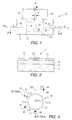
- FIG. 1is a top plan view of a planar voltage tunable dielectric varactor constructed in accordance with the present invention
- FIG. 2is a cross-sectional view of the varactor of FIG. 1, taken along line 2 — 2 ;
- FIGS. 3 a , 3 b and 3 care graphs illustrating the capacitance and loss tangent of voltage tunable varactors constructed in accordance with this invention at various operating frequencies and gap widths;
- FIG. 4is a top plan view of an analog reflective termination phase shifter with a rat-race hybrid coupler, which includes varactors constructed in accordance with the present invention
- FIG. 5is a graph illustrating phase shift produced by the phase shifter of FIG. 4 at various frequencies and bias voltages
- FIG. 6is a top plan view of a loaded line circuit phase shifter with a planar varactor constructed in accordance with the present invention
- FIG. 7is an equivalent circuit representation of the phase shifter of FIG. 7;
- FIGS. 8 a , 8 b and 8 care graphs illustrating simulated performance data for the loaded line phase shifter of FIG. 6;
- FIG. 9is a top view of a fin-line waveguide tunable filter with planar varactors constructed in accordance with the present invention.
- FIG. 10is a graph illustrating measured data for the fin line tunable filter of FIG. 9 .
- FIGS. 1 and 2are top and cross sectional views of a varactor 10 constructed in accordance with this invention.
- the varactor 10includes a substrate 12 having a generally planar top surface 14 .
- a tunable ferroelectric layer 16is positioned adjacent to the top surface of the substrate.
- a pair of metal electrodes 18 and 20are positioned on top of the ferroelectric layer.
- the substrate 12is comprised of a material having a relatively low permittivity such as MgO, Alumina, LaAlO 3 , Sapphire, or a ceramic.
- a low permittivityis a permittivity of less than about 30.
- the tunable ferroelectric layer 16is comprised of a material having a permittivity in a range from about 20 to about 2000, and having a tunability in the range from about 10% to about 80% at a bias voltage of about 10 V/ ⁇ m.
- this layeris preferably comprised of Barium-Strontium Titanate, Ba x Sr 1-x TiO 3 (BSTO), where x can range from zero to one, or BSTO-composite ceramics.
- BSTO compositesinclude, but are not limited to: BSTO—MgO, BSTO—MgAl 2 O 4 , BSTO—CaTiO 3 , BSTO—MgTiO 3 , BSTO—MgSrZrTiO 6 , and combinations thereof.
- the tunable layerin one preferred embodiment has a dielectric permittivity greater than 100 when subjected to typical DC bias voltages, for example, voltages ranging from about 5 volts to about 300 volts.
- a gap 22 of width gis formed between the electrodes 18 and 20 .
- the gap widthmust be optimized to increase ratio of the maximum capacitance C max to the minimum capacitance C min (C max /C min ) and increase the quality facto (Q) of the device.
- the width of this gaphas the most influence on the varactor parameters.
- the optimal width, gwill be determined by the width at which the device has maximum C max /C min and minimal loss tangent.
- a controllable voltage source 24is connected by lines 26 and 28 to electrodes 18 and 20 . This voltage source is used to supply a DC bias voltage to the ferroelectric layer, thereby controlling the permittivity of the layer.
- the varactoralso includes an RF input 30 and an RF output 32 . The RF input and output are connected to electrodes 18 and 20 , respectively, by soldered or bonded connections.
- the varactorsmay use gap widths of less than 5-50 ⁇ m.
- the thickness of the ferroelectric layerranges from about 0.1 ⁇ m to about 20 ⁇ m.
- a sealant 34is positioned within the gap and can be any non-conducting material with a high dielectric breakdown strength to allow the application of high voltage without arcing across the gap.
- the sealantcan be epoxy or polyurethane.
- the other dimension that strongly influences the design of the varactorsis the length, L, of the gap as shown in FIG. 1 .
- the length of the gap Lcan be adjusted by changing the length of the ends 36 and 38 of the electrodes. Variations in the length have a strong effect on the capacitance of the varactor.
- the gap lengthwill optimized for this parameter. Once the gap width has been selected, the capacitance becomes a linear function of the length L. For a desired capacitance, the length L can be determined experimentally, or through computer simulation.
- the thickness of the tunable ferroelectric layeralso has a strong effect on the C max /C min .
- the optimum thickness of the ferroelectric layerswill be determined by the thickness at which the maximum C max /C min occurs.
- the ferroelectric layer of the varactor of FIGS. 1 and 2can be comprised of a thin film, thick film, or bulk ferroelectric material such as Barium-Strontium Titanate, Ba x Sr 1-x TiO 3 (BSTO), BSTO and various oxides, or a BSTO composite with various dopant materials added. All of these materials exhibit a low loss tangent.
- the loss tangentwould range from about 0.0001 to about 0.001.
- the loss tangentwould range from about 0.001 to about 0.01.
- the loss tangentwould range from about 0.005 to about 0.02.
- the electrodesmay be fabricated in any geometry or shape containing a gap of predetermined width.
- the required current for manipulation of the capacitance of the varactors disclosed in this inventionis typically less than 1 ⁇ A.
- the electrode materialis gold.
- other conductorssuch as copper, silver or aluminum, may also be used.
- Goldis resistant to corrosion and can be readily bonded to the RF input and output. Copper provides high conductivity, and would typically be coated with gold for bonding or nickel for soldering.
- FIGS. 1 and 2show a voltage tunable planar varactor having a planar electrode with a predetermined gap distance on a single layer tunable bulk, thick film or thin film dielectric.
- the applied voltageproduces an electric field across the gap of the tunable dielectric that produces an overall change in the capacitance of the varactor.
- the width of the gapcan range from 5 to 50 ⁇ m depending on the performance requirements.
- the varactorcan be in turn integrated into a myriad of tunable devices such as those commonly used in conjunction with semiconductor varactors.
- the preferred embodiments of voltage tunable dielectric varactors of this inventionhave Q factors ranging from about 50 to about 10,000 when operated at frequencies ranging from about 1 GHz to about 40 GHz.
- the capacitance (in pF) and the loss factor (tan ⁇ ) of the varactors measured at 3, 10 and 20 GHz for gap distances of 10 and 20 ⁇ mare shown in FIGS. 3 a , 3 b and 3 c .
- the Q's for the varactorsare approximately the following: 200 at 3 GHz, 80 at 10 GHz, 45-55 at 20 GHz.
- typical Q's for GaAs semiconductor diode varactorsare as follows: 175 at 2 GHz, 35 at 10 GHz and much less at even higher frequency. Therefore at frequencies greater than or equal to 10 GHz the varactors of this invention have much better Q factors.
- FIG. 4shows a top view of a phase shifter 40 having varactors constructed in accordance with the invention for use in the operating range of 1.8 to 1.9 GHz.
- the phase shifter 40includes a rat-race coupler 42 , two reflective terminations 44 , 46 and a bias circuit connected to the varactors as shown in FIG. 1, but not shown in FIG. 4 .
- Each of the reflective terminationsincludes a series combination of a ferroelectric varactor of FIGS. 1 and 2, and an inductor 48 , 50 .
- Two DC blocks 52 and 54are mounted on the arms of the input 56 and output 58 of the rat race coupler respectively.
- the DC blocksmay be constructed in accordance with know techniques, such as by using a surface mounted capacitor with high capacitance or a distribution passband filter.
- phase shifter of FIG. 4were achieved as shown in FIG. 5, in the range of the applied varactor bias voltage of 0 to 300 volts DC.
- the figure of meritis about 110, with a relative phase shift error less than 3% over a frequency range of 1.8 to 1.9 GHz.
- the insertion loss of the phase shifteris about 1.0 dB, which includes 0.5 dB related to mismatching and losses in the metal films.
- the operation temperature of the devicewas 300° K.
- FIG. 6is a top view of a 10 GHz phase shifter 60 based on a loaded line 62 microstrip circuit.
- Two planar ferroelectric varactors 10are incorporated in the gaps 64 , 66 of the line 62 .
- An RF signalis input and output by way of 50-ohm microstrips 68 and 70 respectively.
- the center microstriphas a 40-ohm impedance in this example.
- Quarter-wave radial stubs 72 , 74 , 76 and 78are used as impedance matching.
- the varactorsare tuned by the DC bias applied through contact pad 80 and wire 82 .
- Two DC blocks 84 and 86are similar to those discussed in FIG. 4 .
- FIG. 6without the DC blocks, is shown in FIG. 7 .
- the figure of merit for the phase shifter of FIG. 6is 180 deg/dB over a frequency range of about 0.5 GHz. This device is appropriate for applications where the phase shift requirements are less than 100 degrees.
- FIG. 9is a top view of a tunable filter 88 with four ferroelectric varactors based on a symmetrical fin line in a rectangular waveguide.
- an electrically tunable filteris achieved at room temperature by mounting several ferroelectric varactors on a fin line waveguide.
- the fin line constructionis comprised of three foil copper plates 90 , 92 and 94 with thickness of 0.2 mm placed at the center of the waveguide 96 along its longitudinal axis. Two lateral plates with shorted end fin line resonators 98 and 100 are grounded due to the contact with the waveguide.
- Central plate 92is insulated for DC voltage from the waveguide by mica 102 and 104 and is used to apply the control voltage (U b ) to the tunable dielectric varactors 106 , 108 , 110 and 112 .
- the tunable ferroelectric varactorsare soldered in the end of the fin line resonators between plates 90 and 92 , and plates 94 and 92 .
- Flanges 114 and 116support the plates.
- the frequency response of the filter of FIG. 9is shown in FIG. 10 .
- the filterIn the frequency range of the tuning ⁇ F ⁇ 0.8 GHz ( ⁇ 4%) the filter demonstrates the insertion losses (L 0 ) not more than 0.9 dB and the bandwidth of ⁇ f/f ⁇ 2.0% at the level of L 0 , The reflection coefficient for the central frequency was not more than ⁇ 20 dB for any point of the tuning range.
- this inventionprovides a high frequency high power varactor that surpasses the high frequency (>3 GHz) performance of the semiconductor varactors.
- the utilization of these varactors into tunable devicesis also realized in this invention.
- Several examples of specific applications of the varactors in phase shifters and a tunable filterhave been described. This invention has many practical applications and many other modifications of the disclosed devices may be obvious to those skilled in the art without departing from the spirit and scope of this invention.
- the tunable dielectric varactors of this inventionhave increased RF power handling capability and reduced power consumption and cost.
- the inventionprovides voltage tunable bulk, thick film, and thin film varactors that can be used in room temperature voltage tunable devices such as filters, phase shifters, voltage controlled oscillators, delay lines, and tunable resonators, or any combination thereof.
- Examplesare provided for varactors, fin line tunable filters and phase shifters.
- the fin line filteris comprised of two or more varactors and is based on a symmetrical fin line in a rectangular waveguide.
- the example phase shifterscontain reflective terminations with hybrid couplers and a loaded line circuit with planar varactor incorporation.
- the example phase shifterscan operate at frequencies of 2, 10, 20, and 30 GHz.
Landscapes
- Physics & Mathematics (AREA)
- Electromagnetism (AREA)
- Waveguide Switches, Polarizers, And Phase Shifters (AREA)
- Control Of Motors That Do Not Use Commutators (AREA)
- Inductance-Capacitance Distribution Constants And Capacitance-Resistance Oscillators (AREA)
Abstract
Description
Claims (9)
Priority Applications (1)
| Application Number | Priority Date | Filing Date | Title |
|---|---|---|---|
| US10/223,745US6686814B2 (en) | 1998-10-16 | 2002-08-19 | Voltage tunable varactors and tunable devices including such varactors |
Applications Claiming Priority (3)
| Application Number | Priority Date | Filing Date | Title |
|---|---|---|---|
| US10450498P | 1998-10-16 | 1998-10-16 | |
| US09/419,126US6531936B1 (en) | 1998-10-16 | 1999-10-15 | Voltage tunable varactors and tunable devices including such varactors |
| US10/223,745US6686814B2 (en) | 1998-10-16 | 2002-08-19 | Voltage tunable varactors and tunable devices including such varactors |
Related Parent Applications (1)
| Application Number | Title | Priority Date | Filing Date |
|---|---|---|---|
| US09/419,126ContinuationUS6531936B1 (en) | 1998-10-16 | 1999-10-15 | Voltage tunable varactors and tunable devices including such varactors |
Publications (2)
| Publication Number | Publication Date |
|---|---|
| US20030001692A1 US20030001692A1 (en) | 2003-01-02 |
| US6686814B2true US6686814B2 (en) | 2004-02-03 |
Family
ID=22300851
Family Applications (2)
| Application Number | Title | Priority Date | Filing Date |
|---|---|---|---|
| US09/419,126Expired - LifetimeUS6531936B1 (en) | 1998-10-16 | 1999-10-15 | Voltage tunable varactors and tunable devices including such varactors |
| US10/223,745Expired - LifetimeUS6686814B2 (en) | 1998-10-16 | 2002-08-19 | Voltage tunable varactors and tunable devices including such varactors |
Family Applications Before (1)
| Application Number | Title | Priority Date | Filing Date |
|---|---|---|---|
| US09/419,126Expired - LifetimeUS6531936B1 (en) | 1998-10-16 | 1999-10-15 | Voltage tunable varactors and tunable devices including such varactors |
Country Status (12)
| Country | Link |
|---|---|
| US (2) | US6531936B1 (en) |
| EP (1) | EP1121725B1 (en) |
| JP (1) | JP2002528899A (en) |
| KR (1) | KR20010089308A (en) |
| CN (1) | CN1326599A (en) |
| AT (1) | ATE244459T1 (en) |
| AU (1) | AU1117500A (en) |
| CA (1) | CA2346856A1 (en) |
| DE (1) | DE69909313T2 (en) |
| EA (1) | EA200100448A1 (en) |
| ES (1) | ES2201797T3 (en) |
| WO (1) | WO2000024079A1 (en) |
Cited By (10)
| Publication number | Priority date | Publication date | Assignee | Title |
|---|---|---|---|---|
| US20060208823A1 (en)* | 2005-03-21 | 2006-09-21 | Hunt Andrew T | Tunable dielectric radio frequency microelectromechanical system capacitive switch |
| US20080232023A1 (en)* | 2007-03-22 | 2008-09-25 | James Oakes | Capacitors adapted for acoustic resonance cancellation |
| US20090040687A1 (en)* | 2007-03-22 | 2009-02-12 | James Oakes | Capacitors adapted for acoustic resonance cancellation |
| US20090065814A1 (en)* | 2005-02-11 | 2009-03-12 | Alpha & Omega Semiconductor Limited | MOS device with schottky barrier controlling layer |
| CN102457242A (en)* | 2010-10-14 | 2012-05-16 | 重庆融海超声医学工程研究中心有限公司 | Impedance matching network and design method thereof |
| US8194387B2 (en) | 2009-03-20 | 2012-06-05 | Paratek Microwave, Inc. | Electrostrictive resonance suppression for tunable capacitors |
| US8450794B2 (en) | 2005-02-11 | 2013-05-28 | Alpha & Omega Semiconductor Limited | MOS device with varying contact trench lengths |
| US8597998B2 (en) | 2005-02-11 | 2013-12-03 | Alpha & Omega Semiconductor Limited | Power MOS device fabrication |
| US8637368B2 (en) | 2005-02-11 | 2014-01-28 | Alpha And Omega Semiconductor Incorporated | Fabrication of MOS device with varying trench depth |
| US8928079B2 (en)* | 2005-02-11 | 2015-01-06 | Alpha And Omega Semiconductor Limited | MOS device with low injection diode |
Families Citing this family (150)
| Publication number | Priority date | Publication date | Assignee | Title |
|---|---|---|---|---|
| EP1208613A1 (en)* | 1999-08-24 | 2002-05-29 | Paratek Microwave, Inc. | Voltage tunable coplanar phase shifters |
| AU2001259372A1 (en)* | 2000-05-02 | 2001-11-12 | Paratek Microwave, Inc. | Microstrip phase shifter |
| WO2001084660A1 (en) | 2000-05-02 | 2001-11-08 | Paratek Microwave, Inc. | Voltage tuned dielectric varactors with bottom electrodes |
| US8064188B2 (en) | 2000-07-20 | 2011-11-22 | Paratek Microwave, Inc. | Optimized thin film capacitors |
| US7865154B2 (en)* | 2000-07-20 | 2011-01-04 | Paratek Microwave, Inc. | Tunable microwave devices with auto-adjusting matching circuit |
| US8744384B2 (en) | 2000-07-20 | 2014-06-03 | Blackberry Limited | Tunable microwave devices with auto-adjusting matching circuit |
| EP1301960A1 (en)* | 2000-07-20 | 2003-04-16 | Paratek Microwave, Inc. | Tunable microwave devices with auto-adjusting matching circuit |
| US6683513B2 (en)* | 2000-10-26 | 2004-01-27 | Paratek Microwave, Inc. | Electronically tunable RF diplexers tuned by tunable capacitors |
| US6993107B2 (en)* | 2001-01-16 | 2006-01-31 | International Business Machines Corporation | Analog unidirectional serial link architecture |
| US7174147B2 (en)* | 2001-04-11 | 2007-02-06 | Kyocera Wireless Corp. | Bandpass filter with tunable resonator |
| US6690251B2 (en)* | 2001-04-11 | 2004-02-10 | Kyocera Wireless Corporation | Tunable ferro-electric filter |
| US7221243B2 (en)* | 2001-04-11 | 2007-05-22 | Kyocera Wireless Corp. | Apparatus and method for combining electrical signals |
| WO2002084310A1 (en)* | 2001-04-11 | 2002-10-24 | Kyocera Wireless Corporation | Low-loss tunable ferro-electric device and method of characterization |
| US7746292B2 (en)* | 2001-04-11 | 2010-06-29 | Kyocera Wireless Corp. | Reconfigurable radiation desensitivity bracket systems and methods |
| US7394430B2 (en)* | 2001-04-11 | 2008-07-01 | Kyocera Wireless Corp. | Wireless device reconfigurable radiation desensitivity bracket systems and methods |
| US7154440B2 (en)* | 2001-04-11 | 2006-12-26 | Kyocera Wireless Corp. | Phase array antenna using a constant-gain phase shifter |
| US7164329B2 (en)* | 2001-04-11 | 2007-01-16 | Kyocera Wireless Corp. | Tunable phase shifer with a control signal generator responsive to DC offset in a mixed signal |
| US6617062B2 (en)* | 2001-04-13 | 2003-09-09 | Paratek Microwave, Inc. | Strain-relieved tunable dielectric thin films |
| SE520018C2 (en)* | 2001-05-09 | 2003-05-06 | Ericsson Telefon Ab L M | Ferroelectric devices and method related thereto |
| US6535076B2 (en) | 2001-05-15 | 2003-03-18 | Silicon Valley Bank | Switched charge voltage driver and method for applying voltage to tunable dielectric devices |
| US6710679B2 (en) | 2001-08-16 | 2004-03-23 | Paratek Microwave, Inc. | Analog rat-race phase shifters tuned by dielectric varactors |
| US6801160B2 (en)* | 2001-08-27 | 2004-10-05 | Herbert Jefferson Henderson | Dynamic multi-beam antenna using dielectrically tunable phase shifters |
| US20050200422A1 (en)* | 2001-09-20 | 2005-09-15 | Khosro Shamsaifar | Tunable filters having variable bandwidth and variable delay |
| WO2003026059A1 (en)* | 2001-09-20 | 2003-03-27 | Paratek Microwave, Inc. | Tunable filters having variable bandwidth and variable delay |
| US7071776B2 (en) | 2001-10-22 | 2006-07-04 | Kyocera Wireless Corp. | Systems and methods for controlling output power in a communication device |
| US7180467B2 (en)* | 2002-02-12 | 2007-02-20 | Kyocera Wireless Corp. | System and method for dual-band antenna matching |
| US7184727B2 (en)* | 2002-02-12 | 2007-02-27 | Kyocera Wireless Corp. | Full-duplex antenna system and method |
| US7176845B2 (en)* | 2002-02-12 | 2007-02-13 | Kyocera Wireless Corp. | System and method for impedance matching an antenna to sub-bands in a communication band |
| US20030176179A1 (en)* | 2002-03-18 | 2003-09-18 | Ken Hersey | Wireless local area network and antenna used therein |
| US7183922B2 (en)* | 2002-03-18 | 2007-02-27 | Paratek Microwave, Inc. | Tracking apparatus, system and method |
| US20050113138A1 (en)* | 2002-03-18 | 2005-05-26 | Greg Mendolia | RF ID tag reader utlizing a scanning antenna system and method |
| US7496329B2 (en)* | 2002-03-18 | 2009-02-24 | Paratek Microwave, Inc. | RF ID tag reader utilizing a scanning antenna system and method |
| US7187288B2 (en)* | 2002-03-18 | 2007-03-06 | Paratek Microwave, Inc. | RFID tag reading system and method |
| US20050159187A1 (en)* | 2002-03-18 | 2005-07-21 | Greg Mendolia | Antenna system and method |
| US6987493B2 (en)* | 2002-04-15 | 2006-01-17 | Paratek Microwave, Inc. | Electronically steerable passive array antenna |
| US7107033B2 (en)* | 2002-04-17 | 2006-09-12 | Paratek Microwave, Inc. | Smart radio incorporating Parascan® varactors embodied within an intelligent adaptive RF front end |
| US6864843B2 (en)* | 2002-08-15 | 2005-03-08 | Paratek Microwave, Inc. | Conformal frequency-agile tunable patch antenna |
| US7111520B2 (en)* | 2002-08-26 | 2006-09-26 | Gilbarco Inc. | Increased sensitivity for liquid meter |
| US6854342B2 (en) | 2002-08-26 | 2005-02-15 | Gilbarco, Inc. | Increased sensitivity for turbine flow meter |
| US6960546B2 (en) | 2002-09-27 | 2005-11-01 | Paratek Microwave, Inc. | Dielectric composite materials including an electronically tunable dielectric phase and a calcium and oxygen-containing compound phase |
| US7369828B2 (en)* | 2003-02-05 | 2008-05-06 | Paratek Microwave, Inc. | Electronically tunable quad-band antennas for handset applications |
| US20040178867A1 (en)* | 2003-02-05 | 2004-09-16 | Rahman Mohammed Mahbubur | LTCC based electronically tunable multilayer microstrip-stripline combline filter |
| US20040183626A1 (en)* | 2003-02-05 | 2004-09-23 | Qinghua Kang | Electronically tunable block filter with tunable transmission zeros |
| US20040224649A1 (en)* | 2003-02-05 | 2004-11-11 | Khosro Shamsaifar | Electronically tunable power amplifier tuner |
| US20040227592A1 (en) | 2003-02-05 | 2004-11-18 | Chiu Luna H. | Method of applying patterned metallization to block filter resonators |
| US20050116797A1 (en)* | 2003-02-05 | 2005-06-02 | Khosro Shamsaifar | Electronically tunable block filter |
| US7048992B2 (en)* | 2003-02-05 | 2006-05-23 | Paratek Microwave, Inc. | Fabrication of Parascan tunable dielectric chips |
| US20040185795A1 (en)* | 2003-02-05 | 2004-09-23 | Khosro Shamsaifar | Electronically tunable RF Front End Module |
| US20040251991A1 (en)* | 2003-02-05 | 2004-12-16 | Rahman Mohammed Mahbubur | Electronically tunable comb-ring type RF filter |
| US6949982B2 (en)* | 2003-03-06 | 2005-09-27 | Paratek Microwave, Inc. | Voltage controlled oscillators incorporating parascan R varactors |
| US6967540B2 (en)* | 2003-03-06 | 2005-11-22 | Paratek Microwave, Inc. | Synthesizers incorporating parascan TM varactors |
| US8204438B2 (en)* | 2003-03-14 | 2012-06-19 | Paratek Microwave, Inc. | RF ID tag reader utilizing a scanning antenna system and method |
| WO2004093145A2 (en)* | 2003-04-11 | 2004-10-28 | Paratek Microwave, Inc. | Voltage tunable photodefinable dielectric and method of manufacture therefore |
| EP1618610A2 (en)* | 2003-04-30 | 2006-01-25 | Paratek Microwave, Inc. | Electronically tunable rf chip packages |
| US7042316B2 (en)* | 2003-05-01 | 2006-05-09 | Paratek Microwave, Inc. | Waveguide dielectric resonator electrically tunable filter |
| WO2004107499A2 (en)* | 2003-05-22 | 2004-12-09 | Paratek Microwave Inc. | Wireless local area network antenna system and method of use therefore |
| US7720443B2 (en) | 2003-06-02 | 2010-05-18 | Kyocera Wireless Corp. | System and method for filtering time division multiple access telephone communications |
| US20060035023A1 (en)* | 2003-08-07 | 2006-02-16 | Wontae Chang | Method for making a strain-relieved tunable dielectric thin film |
| US7123115B2 (en)* | 2003-08-08 | 2006-10-17 | Paratek Microwave, Inc. | Loaded line phase shifter having regions of higher and lower impedance |
| WO2005015681A2 (en)* | 2003-08-08 | 2005-02-17 | Paratek Microwave, Inc. | Stacked patch antenna and method of operation therefore |
| KR100546759B1 (en)* | 2003-08-18 | 2006-01-26 | 한국전자통신연구원 | Distributed Integer Analog Phase Shifter Using Etched Ferroelectric Thin Film and Its Manufacturing Method |
| US7142072B2 (en) | 2003-09-22 | 2006-11-28 | Kyocera Corporation | Variable matching circuit, variable resonance circuit, variable phase-shifting circuit and variable attenuation circuit each having variable-capacitance capacitor |
| US6992638B2 (en)* | 2003-09-27 | 2006-01-31 | Paratek Microwave, Inc. | High gain, steerable multiple beam antenna system |
| US7030463B1 (en) | 2003-10-01 | 2006-04-18 | University Of Dayton | Tuneable electromagnetic bandgap structures based on high resistivity silicon substrates |
| WO2005072468A2 (en)* | 2004-01-28 | 2005-08-11 | Paratek Microwave Inc. | Apparatus and method capable of utilizing a tunable antenna-duplexer combination |
| US20050164744A1 (en)* | 2004-01-28 | 2005-07-28 | Du Toit Nicolaas D. | Apparatus and method operable in a wireless local area network incorporating tunable dielectric capacitors embodied within an inteligent adaptive antenna |
| US7268643B2 (en)* | 2004-01-28 | 2007-09-11 | Paratek Microwave, Inc. | Apparatus, system and method capable of radio frequency switching using tunable dielectric capacitors |
| US7145509B2 (en) | 2004-02-17 | 2006-12-05 | Kyocera Corporation | Array antenna and radio communication apparatus using the same |
| US20050206482A1 (en)* | 2004-03-17 | 2005-09-22 | Dutoit Nicolaas | Electronically tunable switched-resonator filter bank |
| US7151411B2 (en)* | 2004-03-17 | 2006-12-19 | Paratek Microwave, Inc. | Amplifier system and method |
| US20060006962A1 (en)* | 2004-07-08 | 2006-01-12 | Du Toit Cornelis F | Phase shifters and method of manufacture therefore |
| US20060006966A1 (en)* | 2004-07-08 | 2006-01-12 | Qinghua Kang | Electronically tunable ridged waveguide cavity filter and method of manufacture therefore |
| US20060006961A1 (en)* | 2004-07-08 | 2006-01-12 | Sengupta L | Tunable dielectric phase shifters capable of operating in a digital-analog regime |
| US20060009185A1 (en)* | 2004-07-08 | 2006-01-12 | Khosro Shamsaifar | Method and apparatus capable of interference cancellation |
| US7248845B2 (en)* | 2004-07-09 | 2007-07-24 | Kyocera Wireless Corp. | Variable-loss transmitter and method of operation |
| US7379711B2 (en)* | 2004-07-30 | 2008-05-27 | Paratek Microwave, Inc. | Method and apparatus capable of mitigating third order inter-modulation distortion in electronic circuits |
| US7519340B2 (en)* | 2004-07-30 | 2009-04-14 | Paratek Microwave, Inc. | Method and apparatus capable of mitigating third order inter-modulation distortion in electronic circuits |
| US20060033593A1 (en)* | 2004-08-13 | 2006-02-16 | Qinghua Kang | Method and apparatus with improved varactor quality factor |
| US20060044204A1 (en)* | 2004-08-14 | 2006-03-02 | Jeffrey Kruth | Phased array antenna with steerable null |
| US7557055B2 (en)* | 2004-09-20 | 2009-07-07 | Paratek Microwave, Inc. | Tunable low loss material composition |
| US20060065916A1 (en) | 2004-09-29 | 2006-03-30 | Xubai Zhang | Varactors and methods of manufacture and use |
| US7397329B2 (en)* | 2004-11-02 | 2008-07-08 | Du Toit Nicolaas D | Compact tunable filter and method of operation and manufacture therefore |
| KR100582548B1 (en)* | 2004-12-20 | 2006-05-22 | 한국전자통신연구원 | Phase Shifter with PPU Structure Using Ferroelectric Thin Film |
| US20060267174A1 (en)* | 2005-02-09 | 2006-11-30 | William Macropoulos | Apparatus and method using stackable substrates |
| US7471146B2 (en)* | 2005-02-15 | 2008-12-30 | Paratek Microwave, Inc. | Optimized circuits for three dimensional packaging and methods of manufacture therefore |
| US7884703B2 (en)* | 2005-03-23 | 2011-02-08 | Crest Electronics, Inc. | Pillow speaker remote control |
| US20070007853A1 (en) | 2005-07-09 | 2007-01-11 | Toit Nicolaas D | Apparatus and method capable of a high fundamental acoustic resonance frequency and a wide resonance-free frequency range |
| US20070007850A1 (en)* | 2005-07-09 | 2007-01-11 | Toit Nicolaas D | Apparatus and method capable of a high fundamental acoustic resonance frequency and a wide resonance-free frequency range |
| US20070007854A1 (en)* | 2005-07-09 | 2007-01-11 | James Oakes | Ripple free tunable capacitor and method of operation and manufacture therefore |
| US8067997B2 (en)* | 2005-11-10 | 2011-11-29 | The Arizona Board Of Regents On Behalf Of The University Of Arizona | Apparatus and method of selecting components for a reconfigurable impedance match circuit |
| US9406444B2 (en) | 2005-11-14 | 2016-08-02 | Blackberry Limited | Thin film capacitors |
| US7548762B2 (en)* | 2005-11-30 | 2009-06-16 | Kyocera Corporation | Method for tuning a GPS antenna matching network |
| US8325097B2 (en)* | 2006-01-14 | 2012-12-04 | Research In Motion Rf, Inc. | Adaptively tunable antennas and method of operation therefore |
| US8125399B2 (en)* | 2006-01-14 | 2012-02-28 | Paratek Microwave, Inc. | Adaptively tunable antennas incorporating an external probe to monitor radiated power |
| US7711337B2 (en) | 2006-01-14 | 2010-05-04 | Paratek Microwave, Inc. | Adaptive impedance matching module (AIMM) control architectures |
| US20070279159A1 (en)* | 2006-06-02 | 2007-12-06 | Heinz Georg Bachmann | Techniques to reduce circuit non-linear distortion |
| KR100747657B1 (en)* | 2006-10-26 | 2007-08-08 | 삼성전자주식회사 | Semiconductor devices capable of macro and micro frequency tuning, and antennas and frequency tuning circuits having them |
| US7714676B2 (en)* | 2006-11-08 | 2010-05-11 | Paratek Microwave, Inc. | Adaptive impedance matching apparatus, system and method |
| US7535312B2 (en)* | 2006-11-08 | 2009-05-19 | Paratek Microwave, Inc. | Adaptive impedance matching apparatus, system and method with improved dynamic range |
| US9201556B2 (en)* | 2006-11-08 | 2015-12-01 | 3M Innovative Properties Company | Touch location sensing system and method employing sensor data fitting to a predefined curve |
| US8299867B2 (en)* | 2006-11-08 | 2012-10-30 | Research In Motion Rf, Inc. | Adaptive impedance matching module |
| US7813777B2 (en)* | 2006-12-12 | 2010-10-12 | Paratek Microwave, Inc. | Antenna tuner with zero volts impedance fold back |
| US8207944B2 (en)* | 2006-12-19 | 2012-06-26 | 3M Innovative Properties Company | Capacitance measuring circuit and method |
| US8040329B2 (en)* | 2006-12-20 | 2011-10-18 | 3M Innovative Properties Company | Frequency control circuit for tuning a resonant circuit of an untethered device |
| US8243049B2 (en) | 2006-12-20 | 2012-08-14 | 3M Innovative Properties Company | Untethered stylus employing low current power converter |
| US7956851B2 (en)* | 2006-12-20 | 2011-06-07 | 3M Innovative Properties Company | Self-tuning drive source employing input impedance phase detection |
| US8134542B2 (en)* | 2006-12-20 | 2012-03-13 | 3M Innovative Properties Company | Untethered stylus employing separate communication and power channels |
| US8040330B2 (en) | 2006-12-28 | 2011-10-18 | 3M Innovative Properties Company | Untethered stylus empolying multiple reference frequency communication |
| US8089474B2 (en) | 2006-12-28 | 2012-01-03 | 3M Innovative Properties Company | Location sensing system and method employing adaptive drive signal adjustment |
| US7787259B2 (en)* | 2006-12-28 | 2010-08-31 | 3M Innovative Properties Company | Magnetic shield for use in a location sensing system |
| KR100813937B1 (en)* | 2007-02-22 | 2008-03-17 | 한국원자력연구원 | Waveguide Array Coupler with Variable Coupling Coefficient |
| US7917104B2 (en)* | 2007-04-23 | 2011-03-29 | Paratek Microwave, Inc. | Techniques for improved adaptive impedance matching |
| US8213886B2 (en) | 2007-05-07 | 2012-07-03 | Paratek Microwave, Inc. | Hybrid techniques for antenna retuning utilizing transmit and receive power information |
| US7991363B2 (en) | 2007-11-14 | 2011-08-02 | Paratek Microwave, Inc. | Tuning matching circuits for transmitter and receiver bands as a function of transmitter metrics |
| US8112852B2 (en)* | 2008-05-14 | 2012-02-14 | Paratek Microwave, Inc. | Radio frequency tunable capacitors and method of manufacturing using a sacrificial carrier substrate |
| US7922975B2 (en)* | 2008-07-14 | 2011-04-12 | University Of Dayton | Resonant sensor capable of wireless interrogation |
| US8072285B2 (en) | 2008-09-24 | 2011-12-06 | Paratek Microwave, Inc. | Methods for tuning an adaptive impedance matching network with a look-up table |
| US8067858B2 (en)* | 2008-10-14 | 2011-11-29 | Paratek Microwave, Inc. | Low-distortion voltage variable capacitor assemblies |
| US20100096678A1 (en)* | 2008-10-20 | 2010-04-22 | University Of Dayton | Nanostructured barium strontium titanate (bst) thin-film varactors on sapphire |
| US8472888B2 (en)* | 2009-08-25 | 2013-06-25 | Research In Motion Rf, Inc. | Method and apparatus for calibrating a communication device |
| US9026062B2 (en) | 2009-10-10 | 2015-05-05 | Blackberry Limited | Method and apparatus for managing operations of a communication device |
| WO2011090933A1 (en)* | 2010-01-21 | 2011-07-28 | Northeastern University | Voltage tuning of microwave magnetic devices using magnetoelectric transducers |
| US8803631B2 (en) | 2010-03-22 | 2014-08-12 | Blackberry Limited | Method and apparatus for adapting a variable impedance network |
| JP5901612B2 (en) | 2010-04-20 | 2016-04-13 | ブラックベリー リミテッド | Method and apparatus for managing interference in a communication device |
| US9379454B2 (en) | 2010-11-08 | 2016-06-28 | Blackberry Limited | Method and apparatus for tuning antennas in a communication device |
| US8712340B2 (en) | 2011-02-18 | 2014-04-29 | Blackberry Limited | Method and apparatus for radio antenna frequency tuning |
| US8655286B2 (en) | 2011-02-25 | 2014-02-18 | Blackberry Limited | Method and apparatus for tuning a communication device |
| US8626083B2 (en) | 2011-05-16 | 2014-01-07 | Blackberry Limited | Method and apparatus for tuning a communication device |
| US8594584B2 (en) | 2011-05-16 | 2013-11-26 | Blackberry Limited | Method and apparatus for tuning a communication device |
| EP2740221B1 (en) | 2011-08-05 | 2019-06-26 | BlackBerry Limited | Method and apparatus for band tuning in a communication device |
| US8948889B2 (en) | 2012-06-01 | 2015-02-03 | Blackberry Limited | Methods and apparatus for tuning circuit components of a communication device |
| US9000866B2 (en) | 2012-06-26 | 2015-04-07 | University Of Dayton | Varactor shunt switches with parallel capacitor architecture |
| US9853363B2 (en) | 2012-07-06 | 2017-12-26 | Blackberry Limited | Methods and apparatus to control mutual coupling between antennas |
| US9246223B2 (en) | 2012-07-17 | 2016-01-26 | Blackberry Limited | Antenna tuning for multiband operation |
| US9413066B2 (en) | 2012-07-19 | 2016-08-09 | Blackberry Limited | Method and apparatus for beam forming and antenna tuning in a communication device |
| US9350405B2 (en) | 2012-07-19 | 2016-05-24 | Blackberry Limited | Method and apparatus for antenna tuning and power consumption management in a communication device |
| US9362891B2 (en) | 2012-07-26 | 2016-06-07 | Blackberry Limited | Methods and apparatus for tuning a communication device |
| US10186903B2 (en)* | 2012-08-28 | 2019-01-22 | Philips Lighting Holding B.V. | Electrical breakdown protection for a capacitive wireless powering system |
| US10404295B2 (en) | 2012-12-21 | 2019-09-03 | Blackberry Limited | Method and apparatus for adjusting the timing of radio antenna tuning |
| US9374113B2 (en) | 2012-12-21 | 2016-06-21 | Blackberry Limited | Method and apparatus for adjusting the timing of radio antenna tuning |
| US9219877B2 (en) | 2013-03-07 | 2015-12-22 | Holland Electronics, Llc | Impedance compensation circuit |
| DE102014210747B4 (en) | 2014-02-12 | 2023-11-16 | Rohde & Schwarz GmbH & Co. Kommanditgesellschaft | Phase locked loop with varactor in microsystem technology |
| US9466868B2 (en) | 2014-04-21 | 2016-10-11 | Globalfoundries Inc. | Reconfigurable branch line coupler |
| CN103956999A (en)* | 2014-04-29 | 2014-07-30 | 中国人民解放军国防科学技术大学 | Integrated phase shifting and pulse compression signal processing device |
| US9461612B2 (en) | 2014-05-22 | 2016-10-04 | Globalfoundries Inc. | Reconfigurable rat race coupler |
| US9438319B2 (en) | 2014-12-16 | 2016-09-06 | Blackberry Limited | Method and apparatus for antenna selection |
| US10720955B2 (en)* | 2016-01-20 | 2020-07-21 | Lg Electronics Inc. | Method for removing magnetic interference signal according to use of FDR scheme, and device for removing magnetic interference signal |
| US11317519B2 (en) | 2018-10-15 | 2022-04-26 | International Business Machines Corporation | Fabrication of superconducting devices that control direct currents and microwave signals |
| DE102018126085A1 (en)* | 2018-10-19 | 2020-04-23 | Forschungsverbund Berlin E.V. | Output filter for an amplifier |
| CN119994423B (en)* | 2025-04-17 | 2025-07-08 | 中天通信技术有限公司 | Tunable cavity filter coupler, antenna device and communication equipment |
Citations (10)
| Publication number | Priority date | Publication date | Assignee | Title |
|---|---|---|---|---|
| US4598424A (en)* | 1983-04-22 | 1986-07-01 | Kabushiki Kaisha Toshiba | Microwave mixer circuit |
| US5032805A (en) | 1989-10-23 | 1991-07-16 | The United States Of America As Represented By The Secretary Of The Army | RF phase shifter |
| US5307033A (en) | 1993-01-19 | 1994-04-26 | The United States Of America As Represented By The Secretary Of The Army | Planar digital ferroelectric phase shifter |
| US5472935A (en) | 1992-12-01 | 1995-12-05 | Yandrofski; Robert M. | Tuneable microwave devices incorporating high temperature superconducting and ferroelectric films |
| US5561407A (en) | 1995-01-31 | 1996-10-01 | The United States Of America As Represented By The Secretary Of The Army | Single substrate planar digital ferroelectric phase shifter |
| US5640042A (en) | 1995-12-14 | 1997-06-17 | The United States Of America As Represented By The Secretary Of The Army | Thin film ferroelectric varactor |
| US5760661A (en) | 1996-07-11 | 1998-06-02 | Northrop Grumman Corporation | Variable phase shifter using an array of varactor diodes for uniform transmission line loading |
| US6096127A (en)* | 1997-02-28 | 2000-08-01 | Superconducting Core Technologies, Inc. | Tuneable dielectric films having low electrical losses |
| US6097263A (en) | 1996-06-28 | 2000-08-01 | Robert M. Yandrofski | Method and apparatus for electrically tuning a resonating device |
| US6377440B1 (en)* | 2000-09-12 | 2002-04-23 | Paratek Microwave, Inc. | Dielectric varactors with offset two-layer electrodes |
Family Cites Families (4)
| Publication number | Priority date | Publication date | Assignee | Title |
|---|---|---|---|---|
| JPS583401B2 (en)* | 1972-05-23 | 1983-01-21 | 日本放送協会 | micro halo |
| JPS5933902A (en)* | 1982-08-19 | 1984-02-24 | Fujitsu Ltd | MIC circuit |
| JPH06216640A (en)* | 1993-01-19 | 1994-08-05 | Fujitsu Ltd | High frequency circuit |
| US5442327A (en)* | 1994-06-21 | 1995-08-15 | Motorola, Inc. | MMIC tunable biphase modulator |
- 1999
- 1999-10-15EAEA200100448Apatent/EA200100448A1/enunknown
- 1999-10-15AUAU11175/00Apatent/AU1117500A/ennot_activeAbandoned
- 1999-10-15CNCN99813275Apatent/CN1326599A/enactivePending
- 1999-10-15ESES99954955Tpatent/ES2201797T3/ennot_activeExpired - Lifetime
- 1999-10-15CACA002346856Apatent/CA2346856A1/ennot_activeAbandoned
- 1999-10-15ATAT99954955Tpatent/ATE244459T1/ennot_activeIP Right Cessation
- 1999-10-15DEDE69909313Tpatent/DE69909313T2/ennot_activeExpired - Fee Related
- 1999-10-15USUS09/419,126patent/US6531936B1/ennot_activeExpired - Lifetime
- 1999-10-15JPJP2000577729Apatent/JP2002528899A/enactivePending
- 1999-10-15EPEP99954955Apatent/EP1121725B1/ennot_activeExpired - Lifetime
- 1999-10-15WOPCT/US1999/024161patent/WO2000024079A1/ennot_activeApplication Discontinuation
- 1999-10-15KRKR1020017004786Apatent/KR20010089308A/ennot_activeWithdrawn
- 2002
- 2002-08-19USUS10/223,745patent/US6686814B2/ennot_activeExpired - Lifetime
Patent Citations (11)
| Publication number | Priority date | Publication date | Assignee | Title |
|---|---|---|---|---|
| US4598424A (en)* | 1983-04-22 | 1986-07-01 | Kabushiki Kaisha Toshiba | Microwave mixer circuit |
| US5032805A (en) | 1989-10-23 | 1991-07-16 | The United States Of America As Represented By The Secretary Of The Army | RF phase shifter |
| US5472935A (en) | 1992-12-01 | 1995-12-05 | Yandrofski; Robert M. | Tuneable microwave devices incorporating high temperature superconducting and ferroelectric films |
| US5721194A (en) | 1992-12-01 | 1998-02-24 | Superconducting Core Technologies, Inc. | Tuneable microwave devices including fringe effect capacitor incorporating ferroelectric films |
| US5307033A (en) | 1993-01-19 | 1994-04-26 | The United States Of America As Represented By The Secretary Of The Army | Planar digital ferroelectric phase shifter |
| US5561407A (en) | 1995-01-31 | 1996-10-01 | The United States Of America As Represented By The Secretary Of The Army | Single substrate planar digital ferroelectric phase shifter |
| US5640042A (en) | 1995-12-14 | 1997-06-17 | The United States Of America As Represented By The Secretary Of The Army | Thin film ferroelectric varactor |
| US6097263A (en) | 1996-06-28 | 2000-08-01 | Robert M. Yandrofski | Method and apparatus for electrically tuning a resonating device |
| US5760661A (en) | 1996-07-11 | 1998-06-02 | Northrop Grumman Corporation | Variable phase shifter using an array of varactor diodes for uniform transmission line loading |
| US6096127A (en)* | 1997-02-28 | 2000-08-01 | Superconducting Core Technologies, Inc. | Tuneable dielectric films having low electrical losses |
| US6377440B1 (en)* | 2000-09-12 | 2002-04-23 | Paratek Microwave, Inc. | Dielectric varactors with offset two-layer electrodes |
Non-Patent Citations (6)
| Title |
|---|
| Arthur R. Von Hippel, "Dielectric Material and Applications", 1959, The Technology Press, 305 and 306.** |
| Gevorgian et al., "Electrically controlled HTSC/ferroelectric coplanar waveguide" IEE Proc.-Microw. Antennas Propag., vol. 141, No. 6, Dec. 1994, pp. 501-503. |
| Kozyrev et al., "Ferroelectric Films: Nonlinear Properties and Applications in Microwave Devices," IEEE MTT-S Digest, Jun. 7, 1998, pp. 985-988. |
| Patent Abstracts of Japan, vol. 8, No. 119, Jun. 5, 1984, JP 59033902A (Fujitsu K.K.), Feb. 24, 1984. |
| Princeton Scientific Cop., Neodymium Gallate.** |
| Prineton Scientific Corp, "Lanthanum Aluminate".** |
Cited By (24)
| Publication number | Priority date | Publication date | Assignee | Title |
|---|---|---|---|---|
| US8450794B2 (en) | 2005-02-11 | 2013-05-28 | Alpha & Omega Semiconductor Limited | MOS device with varying contact trench lengths |
| US10978585B2 (en) | 2005-02-11 | 2021-04-13 | Alpha And Omega Semiconductor Limited | MOS device with island region |
| US10535764B2 (en) | 2005-02-11 | 2020-01-14 | Alpha And Omega Semiconductor Limited | Device and fabrication of MOS device with island region |
| US20090065814A1 (en)* | 2005-02-11 | 2009-03-12 | Alpha & Omega Semiconductor Limited | MOS device with schottky barrier controlling layer |
| US8928079B2 (en)* | 2005-02-11 | 2015-01-06 | Alpha And Omega Semiconductor Limited | MOS device with low injection diode |
| US8637368B2 (en) | 2005-02-11 | 2014-01-28 | Alpha And Omega Semiconductor Incorporated | Fabrication of MOS device with varying trench depth |
| US8597998B2 (en) | 2005-02-11 | 2013-12-03 | Alpha & Omega Semiconductor Limited | Power MOS device fabrication |
| US8362547B2 (en) | 2005-02-11 | 2013-01-29 | Alpha & Omega Semiconductor Limited | MOS device with Schottky barrier controlling layer |
| US7786820B2 (en) | 2005-03-21 | 2010-08-31 | Ngimat Co. | Tunable dielectric radio frequency microelectromechanical system capacitive switch |
| US20060208823A1 (en)* | 2005-03-21 | 2006-09-21 | Hunt Andrew T | Tunable dielectric radio frequency microelectromechanical system capacitive switch |
| US8467169B2 (en) | 2007-03-22 | 2013-06-18 | Research In Motion Rf, Inc. | Capacitors adapted for acoustic resonance cancellation |
| US7936553B2 (en) | 2007-03-22 | 2011-05-03 | Paratek Microwave, Inc. | Capacitors adapted for acoustic resonance cancellation |
| US20080232023A1 (en)* | 2007-03-22 | 2008-09-25 | James Oakes | Capacitors adapted for acoustic resonance cancellation |
| US20090040687A1 (en)* | 2007-03-22 | 2009-02-12 | James Oakes | Capacitors adapted for acoustic resonance cancellation |
| US20110170226A1 (en)* | 2007-03-22 | 2011-07-14 | Paratek Microwave, Inc. | Capacitors adapted for acoustic resonance cancellation |
| US9269496B2 (en) | 2007-03-22 | 2016-02-23 | Blackberry Limited | Capacitors adapted for acoustic resonance cancellation |
| US9142355B2 (en) | 2007-03-22 | 2015-09-22 | Blackberry Limited | Capacitors adapted for acoustic resonance cancellation |
| US8400752B2 (en) | 2007-03-22 | 2013-03-19 | Research In Motion Rf, Inc. | Capacitors adapted for acoustic resonance cancellation |
| US8953299B2 (en) | 2007-03-22 | 2015-02-10 | Blackberry Limited | Capacitors adapted for acoustic resonance cancellation |
| US8693162B2 (en) | 2009-03-20 | 2014-04-08 | Blackberry Limited | Electrostrictive resonance suppression for tunable capacitors |
| US9318266B2 (en) | 2009-03-20 | 2016-04-19 | Blackberry Limited | Electrostrictive resonance suppression for tunable capacitors |
| US8194387B2 (en) | 2009-03-20 | 2012-06-05 | Paratek Microwave, Inc. | Electrostrictive resonance suppression for tunable capacitors |
| CN102457242B (en)* | 2010-10-14 | 2014-12-31 | 重庆融海超声医学工程研究中心有限公司 | Impedance matching network and design method thereof |
| CN102457242A (en)* | 2010-10-14 | 2012-05-16 | 重庆融海超声医学工程研究中心有限公司 | Impedance matching network and design method thereof |
Also Published As
| Publication number | Publication date |
|---|---|
| EP1121725B1 (en) | 2003-07-02 |
| US6531936B1 (en) | 2003-03-11 |
| ATE244459T1 (en) | 2003-07-15 |
| DE69909313D1 (en) | 2003-08-07 |
| ES2201797T3 (en) | 2004-03-16 |
| EA200100448A1 (en) | 2001-10-22 |
| US20030001692A1 (en) | 2003-01-02 |
| CN1326599A (en) | 2001-12-12 |
| CA2346856A1 (en) | 2000-04-27 |
| JP2002528899A (en) | 2002-09-03 |
| KR20010089308A (en) | 2001-09-29 |
| WO2000024079A1 (en) | 2000-04-27 |
| AU1117500A (en) | 2000-05-08 |
| EP1121725A1 (en) | 2001-08-08 |
| DE69909313T2 (en) | 2004-06-03 |
Similar Documents
| Publication | Publication Date | Title |
|---|---|---|
| US6686814B2 (en) | Voltage tunable varactors and tunable devices including such varactors | |
| US6646522B1 (en) | Voltage tunable coplanar waveguide phase shifters | |
| US6377217B1 (en) | Serially-fed phased array antennas with dielectric phase shifters | |
| US6525630B1 (en) | Microstrip tunable filters tuned by dielectric varactors | |
| US7145415B2 (en) | Electrically tunable filters with dielectric varactors | |
| EP2768072A1 (en) | Phase shifting device | |
| US20020014932A1 (en) | Microstrip phase shifter | |
| US6985050B2 (en) | Waveguide-finline tunable phase shifter | |
| EP1530249B1 (en) | Voltage tunable coplanar phase shifters |
Legal Events
| Date | Code | Title | Description |
|---|---|---|---|
| STCF | Information on status: patent grant | Free format text:PATENTED CASE | |
| REMI | Maintenance fee reminder mailed | ||
| FPAY | Fee payment | Year of fee payment:4 | |
| SULP | Surcharge for late payment | ||
| FPAY | Fee payment | Year of fee payment:8 | |
| FEPP | Fee payment procedure | Free format text:PAT HOLDER NO LONGER CLAIMS SMALL ENTITY STATUS, ENTITY STATUS SET TO UNDISCOUNTED (ORIGINAL EVENT CODE: STOL); ENTITY STATUS OF PATENT OWNER: LARGE ENTITY | |
| AS | Assignment | Owner name:RESEARCH IN MOTION RF, INC., DELAWARE Free format text:CHANGE OF NAME;ASSIGNOR:PARATEK MICROWAVE, INC.;REEL/FRAME:028686/0432 Effective date:20120608 | |
| AS | Assignment | Owner name:BLACKBERRY LIMITED, ONTARIO Free format text:ASSIGNMENT OF ASSIGNORS INTEREST;ASSIGNOR:RESEARCH IN MOTION CORPORATION;REEL/FRAME:030909/0933 Effective date:20130710 Owner name:RESEARCH IN MOTION CORPORATION, DELAWARE Free format text:ASSIGNMENT OF ASSIGNORS INTEREST;ASSIGNOR:RESEARCH IN MOTION RF, INC.;REEL/FRAME:030909/0908 Effective date:20130709 | |
| FPAY | Fee payment | Year of fee payment:12 | |
| AS | Assignment | Owner name:NXP USA, INC., TEXAS Free format text:ASSIGNMENT OF ASSIGNORS INTEREST;ASSIGNOR:BLACKBERRY LIMITED;REEL/FRAME:052095/0443 Effective date:20200228 |