US6686275B2 - Method of selectively removing metal nitride or metal oxynitride extrusions from a semmiconductor structure - Google Patents
Method of selectively removing metal nitride or metal oxynitride extrusions from a semmiconductor structureDownload PDFInfo
- Publication number
- US6686275B2 US6686275B2US10/405,201US40520103AUS6686275B2US 6686275 B2US6686275 B2US 6686275B2US 40520103 AUS40520103 AUS 40520103AUS 6686275 B2US6686275 B2US 6686275B2
- Authority
- US
- United States
- Prior art keywords
- extrusions
- memory
- metal
- layer
- wordline
- Prior art date
- Legal status (The legal status is an assumption and is not a legal conclusion. Google has not performed a legal analysis and makes no representation as to the accuracy of the status listed.)
- Expired - Lifetime
Links
Images


Classifications
- H—ELECTRICITY
- H10—SEMICONDUCTOR DEVICES; ELECTRIC SOLID-STATE DEVICES NOT OTHERWISE PROVIDED FOR
- H10D—INORGANIC ELECTRIC SEMICONDUCTOR DEVICES
- H10D64/00—Electrodes of devices having potential barriers
- H10D64/60—Electrodes characterised by their materials
- H10D64/66—Electrodes having a conductor capacitively coupled to a semiconductor by an insulator, e.g. MIS electrodes
- H10D64/661—Electrodes having a conductor capacitively coupled to a semiconductor by an insulator, e.g. MIS electrodes the conductor comprising a layer of silicon contacting the insulator, e.g. polysilicon having vertical doping variation
- H10D64/662—Electrodes having a conductor capacitively coupled to a semiconductor by an insulator, e.g. MIS electrodes the conductor comprising a layer of silicon contacting the insulator, e.g. polysilicon having vertical doping variation the conductor further comprising additional layers, e.g. multiple silicon layers having different crystal structures
- H10D64/664—Electrodes having a conductor capacitively coupled to a semiconductor by an insulator, e.g. MIS electrodes the conductor comprising a layer of silicon contacting the insulator, e.g. polysilicon having vertical doping variation the conductor further comprising additional layers, e.g. multiple silicon layers having different crystal structures the additional layers comprising a barrier layer between the layer of silicon and an upper metal or metal silicide layer
- H—ELECTRICITY
- H01—ELECTRIC ELEMENTS
- H01L—SEMICONDUCTOR DEVICES NOT COVERED BY CLASS H10
- H01L21/00—Processes or apparatus adapted for the manufacture or treatment of semiconductor or solid state devices or of parts thereof
- H01L21/02—Manufacture or treatment of semiconductor devices or of parts thereof
- H01L21/04—Manufacture or treatment of semiconductor devices or of parts thereof the devices having potential barriers, e.g. a PN junction, depletion layer or carrier concentration layer
- H01L21/18—Manufacture or treatment of semiconductor devices or of parts thereof the devices having potential barriers, e.g. a PN junction, depletion layer or carrier concentration layer the devices having semiconductor bodies comprising elements of Group IV of the Periodic Table or AIIIBV compounds with or without impurities, e.g. doping materials
- H01L21/28—Manufacture of electrodes on semiconductor bodies using processes or apparatus not provided for in groups H01L21/20 - H01L21/268
- H01L21/28008—Making conductor-insulator-semiconductor electrodes
- H01L21/28017—Making conductor-insulator-semiconductor electrodes the insulator being formed after the semiconductor body, the semiconductor being silicon
- H01L21/28026—Making conductor-insulator-semiconductor electrodes the insulator being formed after the semiconductor body, the semiconductor being silicon characterised by the conductor
- H01L21/28035—Making conductor-insulator-semiconductor electrodes the insulator being formed after the semiconductor body, the semiconductor being silicon characterised by the conductor the final conductor layer next to the insulator being silicon, e.g. polysilicon, with or without impurities
- H01L21/28044—Making conductor-insulator-semiconductor electrodes the insulator being formed after the semiconductor body, the semiconductor being silicon characterised by the conductor the final conductor layer next to the insulator being silicon, e.g. polysilicon, with or without impurities the conductor comprising at least another non-silicon conductive layer
- H01L21/28061—Making conductor-insulator-semiconductor electrodes the insulator being formed after the semiconductor body, the semiconductor being silicon characterised by the conductor the final conductor layer next to the insulator being silicon, e.g. polysilicon, with or without impurities the conductor comprising at least another non-silicon conductive layer the conductor comprising a metal or metal silicide formed by deposition, e.g. sputter deposition, i.e. without a silicidation reaction
- H—ELECTRICITY
- H01—ELECTRIC ELEMENTS
- H01L—SEMICONDUCTOR DEVICES NOT COVERED BY CLASS H10
- H01L21/00—Processes or apparatus adapted for the manufacture or treatment of semiconductor or solid state devices or of parts thereof
- H01L21/02—Manufacture or treatment of semiconductor devices or of parts thereof
- H01L21/04—Manufacture or treatment of semiconductor devices or of parts thereof the devices having potential barriers, e.g. a PN junction, depletion layer or carrier concentration layer
- H01L21/18—Manufacture or treatment of semiconductor devices or of parts thereof the devices having potential barriers, e.g. a PN junction, depletion layer or carrier concentration layer the devices having semiconductor bodies comprising elements of Group IV of the Periodic Table or AIIIBV compounds with or without impurities, e.g. doping materials
- H01L21/28—Manufacture of electrodes on semiconductor bodies using processes or apparatus not provided for in groups H01L21/20 - H01L21/268
- H01L21/28008—Making conductor-insulator-semiconductor electrodes
- H01L21/28017—Making conductor-insulator-semiconductor electrodes the insulator being formed after the semiconductor body, the semiconductor being silicon
- H01L21/28247—Making conductor-insulator-semiconductor electrodes the insulator being formed after the semiconductor body, the semiconductor being silicon passivation or protection of the electrode, e.g. using re-oxidation
- H—ELECTRICITY
- H01—ELECTRIC ELEMENTS
- H01L—SEMICONDUCTOR DEVICES NOT COVERED BY CLASS H10
- H01L21/00—Processes or apparatus adapted for the manufacture or treatment of semiconductor or solid state devices or of parts thereof
- H01L21/02—Manufacture or treatment of semiconductor devices or of parts thereof
- H01L21/04—Manufacture or treatment of semiconductor devices or of parts thereof the devices having potential barriers, e.g. a PN junction, depletion layer or carrier concentration layer
- H01L21/18—Manufacture or treatment of semiconductor devices or of parts thereof the devices having potential barriers, e.g. a PN junction, depletion layer or carrier concentration layer the devices having semiconductor bodies comprising elements of Group IV of the Periodic Table or AIIIBV compounds with or without impurities, e.g. doping materials
- H01L21/30—Treatment of semiconductor bodies using processes or apparatus not provided for in groups H01L21/20 - H01L21/26
- H01L21/31—Treatment of semiconductor bodies using processes or apparatus not provided for in groups H01L21/20 - H01L21/26 to form insulating layers thereon, e.g. for masking or by using photolithographic techniques; After treatment of these layers; Selection of materials for these layers
- H01L21/3205—Deposition of non-insulating-, e.g. conductive- or resistive-, layers on insulating layers; After-treatment of these layers
- H01L21/321—After treatment
- H01L21/3213—Physical or chemical etching of the layers, e.g. to produce a patterned layer from a pre-deposited extensive layer
- H01L21/32133—Physical or chemical etching of the layers, e.g. to produce a patterned layer from a pre-deposited extensive layer by chemical means only
- H01L21/32134—Physical or chemical etching of the layers, e.g. to produce a patterned layer from a pre-deposited extensive layer by chemical means only by liquid etching only
Definitions
- the inventionrelates generally to the removal of extrusions that form during the fabrication of integrated circuits. More particularly, the invention relates to the removal of extrusions that form on metal-oxide-semiconductor (MOS) structures.
- MOSmetal-oxide-semiconductor
- DRAMdynamic random access memory
- Titanium silicideknown for its low resistance
- TiSi xtitanium silicide
- titanium silicideknown for its low resistance
- titanium silicidecan become unstable during subsequent high temperature processing steps and can diffuse into the underlying gate layer (typically polysilicon), also called titanium silicide agglomeration, thereby damaging the semiconductor structure.
- some manufacturerscover the gate layer with a barrier layer, such as titanium nitride (TiN).
- TiNtitanium nitride
- the titanium nitridemay possess a high resistance and thus detract from the low resistance effect of the conductive layer.
- titanium nitridecan oxidize to form titanium oxynitride (TiO x N y ).
- metal silicide layersthat may be exposed to nitrogen and oxygen rich environments at high temperature. These gases react with metal rich portions of the semiconductor structure to create metal oxynitrides. Such metal oxynitrides may expand to create extrusions which protrude outwardly from the sides of the semiconductor structure. If these extrusions contact other portions of the semiconductor, short circuits result.
- a conductorpreferably composed of a tungsten silicide (WSi x ) barrier layer and a titanium silicide (TiSi x ) conductive layer, is disclosed for use in a semiconductor structure such as a wordline, transistor or any other structure.
- a novel wet etchpreferably composed of an oxidizing and chelating agent in solution, is further disclosed for selectively removing extrusions which may protrude from the conductor.
- Exemplary methods of creating the conductorinclude sputtering tungsten silicide onto a polysilicon gate to create a tungsten silicide layer. Titanium silicide is then sputtered onto the tungsten silicide layer.
- Exemplary formulations of the wet etchinclude a combination of an oxidizing agent such as hydrogen peroxide (H 2 O 2 ) in water with a quantity of a chelating agent such as ethylenediaminetetraacetic acid (EDTA).
- the wet etchcomprises water, an oxidizing agent, a chelating agent and a base such as ammonium hydroxide.
- the wet etchcomprises water, an oxidizing agent, a chelating agent, a base and a buffer salt such as ammonium phosphate.
- One aspect of the inventionrelates to a method of fabricating a wordline in a memory array.
- the methodcomprises depositing a tungsten silicide barrier layer on a wordline stack and processing the wordline stack such that tungsten nitride extrusions extend from an exposed surface of the barrier layer.
- the methodfurther comprises selectively etching the tungsten nitride extrusions with a solution that comprises water, hydrogen peroxide and EDTA.
- Another aspect of the inventionrelates to a method of fabricating a wordline in a memory array.
- the methodcomprises depositing a metal silicide layer on a wordline stack and processing the wordline stack such that metal nitride extrusions extend from the metal silicide layer.
- the methodfurther comprises selectively etching the metal nitride extrusions with a solution that comprises at least an oxidizing agent and a chelating agent.
- An additional aspect of the inventionrelates to a method of fabricating a wordline in a memory array.
- the methodcomprises depositing a tungsten silicide barrier layer on a wordline stack and depositing a titanium silicide conductive layer above the tungsten silicide barrier layer.
- the methodfurther comprises processing the wordline stack such that metal nitride extrusions extend from the tungsten silicide barrier layer and the titanium silicide conductive layer.
- the methodalso comprises etching the metal nitride extrusions at a faster rate than the conductive layer or the barrier layer.
- One embodiment of the inventionrelates to a method of fabricating a semiconductor structure.
- the methodcomprises depositing a polysilicon gate on a semiconductor substrate to form a wordline stack and depositing a conductive layer comprising metal silicide above the polysilicon gate.
- the methodfurther comprises processing the wordline stack in a manner that forms protrusions on the conductive layer and etching the protrusions at a faster rate than the conductive layer.
- Another embodiment of the inventionrelates to a method of forming a wordline gate that comprises forming metal nitride extrusions on a wordline stack and selectively removing the metal nitride extrusions.
- An additional embodimentrelates to a method of forming a semiconductor structure. The method comprises selectively removing metal oxynitride extrusions from a semiconductor structure in a manner that does not substantially damage a conductive layer in the semiconductor structure.
- Yet another embodimentrelates to a method of removing metal oxynitride extrusions from a semiconductor structure in a manner that does not substantially damage a polysilicon layer in the semiconductor structure.
- a further embodimentrelates to a method of forming a wordline gate. The method comprises forming metal oxynitride extrusions on a wordline stack and selectively removing the metal oxynitride extrusions.
- One aspect of the inventionrelates to a wet etch for selectively removing tungsten nitride extrusions that comprises at least 10% by weight hydrogen peroxide and at least 0.03% by weight EDTA.
- Another aspect of the inventionrelates to a wet etch for selectively removing metal nitride extrusions that comprises at least 10% by weight an and at least 0.03% by weight a chelating agent.
- One embodiment of the inventionrelates to a semiconductor structure that comprises a tungsten silicide layer, wherein the tungsten silicide layer has substantially etched tungsten nitride extrusions formed thereon.
- Another embodimentrelates to a semiconductor structure that comprises a tungsten silicide layer, wherein the tungsten silicide layer has substantially etched tungsten oxynitride extrusions thereon.
- An additional embodimentrelates to a semiconductor structure that comprises a titanium silicide layer, wherein the titanium silicide layer has substantially etched titanium nitride extrusions thereon.
- Yet another embodimentrelates to a semiconductor structure that comprises a titanium silicide layer, wherein the titanium silicide layer has substantially etched titanium oxynitride extrusions thereon.
- Another aspect of the inventionrelates to a semiconductor structure that comprises a barrier layer above a semiconductor substrate, the barrier layer comprising a tungsten silicide.
- the semiconductor structurefurther comprises a conductive layer above the wordline gate, the conductive layer comprising titanium silicide.
- the semiconductor structurealso comprises a cap above the conductive layer.
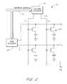
- FIG. 1is a diagram depicting communication between a microprocessor and a memory device.
- FIG. 2shows a memory array containing multiple wordlines and bitlines.
- FIG. 3is a cross-sectional view of a wordline in accordance with one embodiment of the invention.
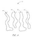
- FIG. 4shows a top view of wordline stacks in a memory array.
- FIG. 5is a top angled view of a wordline stack after source/drain reoxidation and before wet cleaning.
- FIG. 6is a top angled view of a wordline stack after wet cleaning.
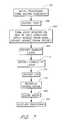
- FIG. 7is a processing flow diagram illustrating the processing blocks for one embodiment of wordline stack fabrication.
- a conductorpreferably composed of a tungsten silicide (WSi x ) barrier layer and a titanium silicide (TiSi x ) conductive layer, is disclosed for use in a semiconductor structure such as a wordline, transistor or any other structure.
- a wet etchpreferably composed of an oxidizing and chelating agent in solution, is further disclosed for removing extrusions which may protrude from these low-resistance segments.
- a novel memory array 10is disclosed herein that interfaces with other electronic circuitry 12 via conventional address signals 14 and data signals 16 .
- the address signals 14select one or more memory cells in the memory array 10 .
- the data signals 16carry data that is stored in or retrieved from the memory array 10 .
- the memory array 10 disclosed hereinis a synchronous dynamic random access memory (SDRAM).
- SDRAMsynchronous dynamic random access memory
- the memory array 10may comprise a wide variety of memory devices such as static memory, dynamic memory, extended data out memory or any other memory type known in the art.
- the memory array 10interfaces with different types of electronic circuitry 12 .
- the electronic circuitry 12can include any device, which accesses or relies on memory including, but not limited to, processors, controllers, and the like.
- the memory array 10 and the electronic circuitry 12are implemented separately, in other embodiments the memory array 10 and the electronic circuitry 12 are integrated together.
- the memory array 10can be implemented in a wide variety of devices, products and systems.
- FIG. 2illustrates a memory array 10 that comprises a plurality of memory cells 20 . These memory cells 20 are organized into columns C N and rows R N . A column decoder 24 and a row decoder 26 process the address signals 14 to identify the column C N and row R N of the targeted memory cells 20 .
- the columnsare commonly known as bitlines and the rows are typically known as wordlines to those skilled in the art.
- FIG. 3illustrates a cross-sectional view of a wordline R N
- FIG. 7illustrates an associated method for making one embodiment of the wordline R N
- a semiconductor substrate 30formed in a processing block 154 , comprises two field oxide regions, 32 and 34 .
- the semiconductor substrate 30may include semiconductor structures and/or other layers that have been fabricated thereon in a processing block 158 or any doped silicon platform that is commonly used in the art. While the illustrated semiconductor substrate 30 comprises an intrinsically doped monocrystalline silicon wafer, it will be understood by one of skill in the art of semiconductor fabrication that the semiconductor substrate 30 in other arrangements can comprise other forms of semiconductor layers which include active or operable portions of semiconductor devices.
- the semiconductor substrate 30is further processed in processing block 162 to create a gate comprising two n+ regions using methods common to those of skill in the art.
- the first n+ region 40acts as a source and the second n+ region 42 acts as a drain.
- the first n+ region 40will be referred to as the source 40 and the second n+ region 42 will be referred to as the drain 42 .
- Each wordline R Nfurther comprises a plurality of layers, which will herein be called a wordline stack 50 .
- the layers in the wordline stack 50comprises a dielectric layer 60 , a polysilicon layer 70 , a conductive segment 80 and a cap 90 .
- the dielectric layer 60is a gate oxide comprising silicon dioxide (SiO 2 ).
- the dielectric layer 60is applied by wet or dry oxidation of the semiconductor substrate 30 followed by etching through a mask, or by other techniques common to those of skill in the art.
- the dielectric layer 60is approximately 60-90 angstroms ( ⁇ ) thick.
- the polysilicon layer 70in one embodiment, may be deposited onto the dielectric layer 60 through chemical vapor in the art. In one embodiment, the polysilicon layer 70 is approximately 1,000 ⁇ thick.
- the conductive segment 80interconnects the source 40 and drain 42 .
- the conductive segment 80comprises a conductive layer 100 and an optional barrier layer 102 .
- the conductive layer 100is typically a metal layer that forms a metal-poly gate.
- the conductive layer 100when implemented over the polysilicon layer 70 , lowers the overall resistivity of the wordlines R N while retaining the gate integrity provided by the polysilicon layer 70 .
- the conductive layer 100comprises a layer of metal silicide.
- One of the functions of the conductive layer 100is to carry the charge to the memory cells 20 in communication with a wordline R N .
- the conductive layer 100is comprised of titanium silicide (TiSi x ) which is deposited in a processing block 170 by physical vapor deposition in an Argon environment.
- TiSi xtitanium silicide
- Suitable sputtering reactorsare commercially available from Applied Materials of Santa Clara, Calif.
- argon gasis introduced into the sputtering chamber at a rate of between about 50 standard cubic centimeters per minute (sccm) and 100 sccm for approximately 8 to 10 seconds.
- the DC magnetron power of the preferred sputtering reactoris generally set at approximately 1.0 kilowatts (kW) to approximately 2.0 kW, preferably at approximately 1.5 kW. In light of the present disclosure, however, the skilled artisan can readily determine the appropriate sputtering parameters through routine optimization to achieve the desired titanium silicide composition in a given reactor configuration.
- the conductive layer 100is approximately 1,000 ⁇ thick and has a resistivity of approximately 15-20 ⁇ -cm.
- the conductive layer 100may also posses metal-rich pockets. For example, if the conductive layer 100 comprises titanium silicide, titanium-rich pockets may exist in the conductive layer 100 .
- the conductive layer 100may also be made from a variety of metals. Additional examples of suitable metals for forming the conductive layer 100 include, but are not limited to, copper, gold, aluminum, silicon, cobalt silicide, nickel silicide, and the like. Mixtures of metals are also suitable for forming the conductive layer 100 . Exemplary methods of depositing the conductive layer 100 include, but are not limited to, Rapid Thermal Chemical Vapor Deposition (RTCVD), Low Pressure Chemical Vapor Deposition (LPCVD), and Physical Vapor Deposition (PVD).
- RTCVDRapid Thermal Chemical Vapor Deposition
- LPCVDLow Pressure Chemical Vapor Deposition
- PVDPhysical Vapor Deposition
- portions of the conductive layer 100may diffuse into the polysilicon layer 70 , thereby damaging the polysilicon layer 70 .
- the conductive layer 100comprises titanium silicide
- the stability of the titanium silicidedecreases when the semiconductor structure is exposed to temperatures exceeding 850° C. during further processing.
- the titanium silicidetends to diffuse into the polysilicon layer 70 thereby degrading the polysilicon.
- the barrier layer 102exists between the conductive layer 100 and the polysilicon layer 70 . In other embodiments, the barrier layer 102 may not exist. While the barrier layer 102 electrically connects the conductive layer 100 and the polysilicon layer 70 , it also inhibits diffusion of impurities between those layers and protects the polysilicon layer 70 during further processing as described below. In one embodiment, the barrier layer 102 comprises a variety of metal silicides such as tungsten silicide (WSi x ) which is deposited in a processing block 166 by physical vapor deposition in an argon environment.
- WSi xtungsten silicide
- Suitable sputtering reactorsare commercially available from Applied Materials of Santa Clara, Calif.
- argon gasis introduced into the sputtering chamber at a rate of between about 50 standard cubic centimeters per minute (sccm) and 100 sccm for approximately 5 to 10 seconds.
- the DC magnetron power of the preferred sputtering reactoris generally set at approximately 0.5 kilowatts (kW) to approximately 2.0 kW, preferably at approximately 1.0 kW.
- the applied tungsten siliconis approximately WSi 2.7 .
- the tungsten silicideremains stable up to temperatures of approximately 1050° C., thereby protecting the polysilicon layer 70 during high temperature anneals and other high-temperature processing.
- the barrier layer 102is approximately 150 ⁇ thick and has a resistivity of approximately 60 ⁇ -cm. The thinness of the barrier layer 102 combined with the low resistance of tungsten silicide improves gate access.
- the skilled artisancan readily determine the appropriate sputtering parameters through routine optimization to achieve the desired barrier layer 102 composition in a given reactor configuration.
- the thickness and resistivity of the barrier layer 102can vary over a range of values.
- the barrier layer 102can comprise a variety of materials such as titanium nitride, silicon nitride or other materials, which protect the polysilicon layer 70 .
- the wordline stack 50further comprises the cap 90 , which is deposited in a processing block 174 onto the conductive segment 80 to protect the underlying materials during further processing.
- the cap 90comprises a layer of silicon oxide (SiO 2 ) which is deposited onto the conductive layer by chemical vapor deposition, or by other techniques common to those of skill in the art.
- the cap 90further comprises a layer of silicon nitride (Si 3 N 4 ) which is deposited onto the silicon oxide layer by chemical vapor deposition, or by other techniques common to those of skill in the art.
- the cap 90comprises silicon nitride as the primary passivating layer.
- the cap 90may be made of various common insulating materials or their combination.
- the wordline stack 50is further patterned through etching.
- FIG. 4illustrates a top view of several wordline stacks in one embodiment of a memory array 10 .
- Each wordline stack 50 in this embodimentis “S” shaped.
- the etchcomprises a level 50 in-situ dry etch.
- the etchmay also comprise other dry or wet etches common to those of skill in the art.
- the patterningstops at the gate oxide 60 or the substrate 30 , and then the source 40 and the drain 42 regions are formed.
- the source 40 and the drain 42are doped with n-type dopants using techniques common to those of skill in the art.
- the wordline stack 50is often exposed to nitrogen rich environments.
- the nitrogenmay react with metal rich pockets in the conductive segment 80 .
- the barrier layer 102comprises tungsten silicide with tungsten-rich pockets
- the tungsten rich pocketsmay react with the nitrogen to form tungsten nitride (WN x ).
- the titanium-rich pocketsmay also react with the nitrogen to form titanium nitride (TiN x ).
- a source/drain reoxidationis applied in a processing block 178 to partly fix dry etch damage and to improve device reliability.
- This reoxidationsubjects the memory array 10 to an oxygen rich environment. While the oxygen reoxidizes the areas existing near the source and drain, the oxygen may also combine with the tungsten nitride and titanium nitride areas existing in the conductive layer 100 and the barrier layer 102 in various embodiments.
- metal oxynitridessuch as tungsten oxynitride (WO x N y ) and titanium oxynitride (TiO x N y ) are formed.
- titanium-rich and tungsten-rich areasmay combine with nitrogen and then oxygen to form titanium tungsten oxynitrides (TiWO x N y ).
- TiWO x N ytitanium tungsten oxynitrides
- other metals in the barrier or conductive layerscan combine with oxygen to create different types of metal oxynitrides.
- the extrusions 140may comprise tungsten oxynitride, titanium oxynitride, and/or titanium tungsten oxynitride. These extrusions 140 not only extend outward from the exposed surface of the conductive layer 100 , but also extend outward from the exposed surface of the barrier layer 102 . While the dimensions of the extrusions 140 vary, the width is typically less than 10 nm and the length is approximately 30 nm to approximately 50 nm.
- these extrusions 140can cause shorts in the memory array 10 .
- 360 memory arrays with a titanium silicide conductive layer 100 and a tungsten silicide barrier layer 102were constructed on a single wafer. After the wafer was processed, only 10 of the 360 memory arrays operated properly.
- extrusions 140have been described with respect to the barrier layer 102 and conductive layer 100 of a wordline stack 50 , it should be understood that such extrusions 140 can develop in a wide range of devices which use metal-based conductors such as transistors and the like.
- the extrusions 140can develop on a wide variety of metal silicides, which are then exposed to nitridizing conditions.
- the extrusions 140can develop metal nitrides, which are exposed to oxidizing conditions.
- the extrusions 140can be removed in a processing block 182 by a unique technique which allows for selective dissolution of the extrusions 140 without significantly harming the materials of the wordline stack 50 .
- a memory array 10is subjected to a novel wet etch that removes the extrusions 140 , as illustrated in FIG. 6 .
- the novel wet etchcomprises an oxidizing agent and a chelating agent in solution.
- the oxidizing agentis hydrogen peroxide (H 2 O 2 ).
- the wet etchis approximately 10% by weight hydrogen peroxide.
- the amount of hydrogen peroxidecan vary from 2% to 50%.
- the oxidizing agentcan include any of a variety of substances including, but not limited to, ozonated water, ozone, nitric acid (HNO3), hypochlorous acid (HClO), chloric acid (HClO 3 ), ammonium persulphate ((NH 4 ) 2 S 2 O 8 ), sulfuric acid (H 2 SO 4 ), and the like.
- the chelating agentis ethylenediaminetetraacetic acid (EDTA) that is approximately 0.03% by weight EDTA.
- EDTAethylenediaminetetraacetic acid
- the amount of EDTA in the wet etchcan range from approximately less than 0.001% to more than 5% by weight EDTA.
- the chelating agentcan be any of a variety of substances including, but not limited to, ligands, the amine group, the carboxylic acid group compounds, oxalate, acetate, disodium ethylenediamine acid (H 2 NC 2 H 4 NH 2 ), glycine (NH 2 CH 2 COOH), iminodiacetic acid (NH(CH 2 COOH)O 2 ), nitrolotriacetic acid (N(CH 2 COOH) 3 ), tetraammonium ethylenediaminetetraacetate, tetramethylammonium ethylenediaminetetraacetate, and the like.
- ligandsthe amine group, the carboxylic acid group compounds, oxalate, acetate, disodium ethylenediamine acid (H 2 NC 2 H 4 NH 2 ), glycine (NH 2 CH 2 COOH), iminodiacetic acid (NH(CH 2 COOH)O 2 ), nitrolotriacetic acid (N(CH 2 CO
- the etchcomprises a combination of an oxidizing and chelating agent and further comprises a base.
- the basemay be used to adjust the pH of the etch solution to improve cleaning and selectivity.
- the baseis ammonium hydroxide (NH 4 OH).
- the wet etchis approximately 0.02% ammonium hydroxide, 0.042% EDTA and 10% hydrogen peroxide and has a pH of about seven to eight.
- the amount of ammonium hydroxidecan vary over a wide range such as from approximately 0.5% to approximately 30% by weight, depending on the desired pH.
- the basecan be any of a variety of bases including, but not limited to, tetramethyl ammonium hydroxide (TMAH), trimethoxyamphetamine (TMA), choline hydroxide, sodium hydroxide, potassium hydroxide, and the like.
- TMAHtetramethyl ammonium hydroxide
- TMAtrimethoxyamphetamine
- choline hydroxidesodium hydroxide
- potassium hydroxidepotassium hydroxide
- the etch solutioncomprises a combination of an oxidizing agent, a chelating agent, a base and a buffer salt.
- the buffer saltmay be added to help maintain a constant pH level and to form a protective layer on the other materials of the stack to assist selectivity.
- the buffer saltis potassium sulfate (K2SO4) that is approximately 2% potassium sulfate.
- the amount of potassium sulfatecan vary over a wide range, depending on the pH and concentration of other substances in the wet etch solution.
- the buffer saltcan be any of a variety of salts including, but not limited to, potassium phosphate, diammonium phosphate, and the like.
- the wet etchis heated to 65° C. It has been found that a 65° C. wet etch comprising 10% hydrogen peroxide and 0.03% EDTA in water removes tungsten nitride at approximately 2040 ⁇ /min. and titanium nitride at approximately 200 ⁇ /min. This wet etch further removes tungsten oxynitride at approximately 200 ⁇ /min. Estimates indicate that the wet etch also removes titanium oxynitride at approximately 20 ⁇ /min. In contrast, the wet etch removes tungsten silicide, titanium silicide, and polysilicon at lower rates such as, by way of example, at approximately 1 ⁇ /min. The rate of etching of the tungsten oxynitride, the titanium oxynitride, the tungsten silicide, the titanium silicide and the polysilicon however, can vary.
- the temperature of the wet etchmay vary over a wide range.
- the temperature of the wet etchvaries from approximately room temperature to approximately 85° C.
- the temperature of the wet etchcan be adjusted based on the composition of the etch solution and the composition of the extrusions 140 to be dissolved.
- ammonium hydroxideis added to adjust the pH of the wet etch.
- 0.02% by weight of ammonium hydroxideadjusts the pH of the wet etch to approximately 7.
- the pH adjustment of the wet etchenhances the metal nitride removal rates without significantly damaging the remainder of the wordline stack 50 .
- a memory array 10is soaked in the preferred wet etch for approximately 2 minutes to remove approximately 50 nm of tungsten oxynitride extrusions 140 .
- the length of time of cleaningcan vary over a wide range. For example, in certain embodiments, the length of time of cleaning varies from approximately 5 minutes to approximately 30 minutes.
- a memory array 10can be soaked in a wet etch solution for enough time to remove as much metal nitride and/or metal oxynitride as required.
- a second 360 memory array waferwas constructed.
- 200 of the 360 memory arraysoperated properly after wet etch cleaning.
- the memory array 10is ready for further processing, in a processing block 190 , as may be required.
Landscapes
- Engineering & Computer Science (AREA)
- Physics & Mathematics (AREA)
- Condensed Matter Physics & Semiconductors (AREA)
- General Physics & Mathematics (AREA)
- Manufacturing & Machinery (AREA)
- Computer Hardware Design (AREA)
- Microelectronics & Electronic Packaging (AREA)
- Power Engineering (AREA)
- Chemical & Material Sciences (AREA)
- Chemical Kinetics & Catalysis (AREA)
- General Chemical & Material Sciences (AREA)
- Semiconductor Memories (AREA)
Abstract
Description
Claims (21)
Priority Applications (1)
| Application Number | Priority Date | Filing Date | Title |
|---|---|---|---|
| US10/405,201US6686275B2 (en) | 1999-08-30 | 2003-04-01 | Method of selectively removing metal nitride or metal oxynitride extrusions from a semmiconductor structure |
Applications Claiming Priority (4)
| Application Number | Priority Date | Filing Date | Title |
|---|---|---|---|
| US09/385,396US6358788B1 (en) | 1999-08-30 | 1999-08-30 | Method of fabricating a wordline in a memory array of a semiconductor device |
| US09/738,796US6455906B2 (en) | 1999-08-30 | 2000-12-15 | Gate stack structure with conductive silicide segment that has substantially etched nitride and/or oxynitride defects protruding from its sidewalls |
| US10/234,577US6693354B2 (en) | 1999-08-30 | 2002-08-30 | Semiconductor structure with substantially etched nitride defects protruding therefrom |
| US10/405,201US6686275B2 (en) | 1999-08-30 | 2003-04-01 | Method of selectively removing metal nitride or metal oxynitride extrusions from a semmiconductor structure |
Related Parent Applications (1)
| Application Number | Title | Priority Date | Filing Date |
|---|---|---|---|
| US10/234,577ContinuationUS6693354B2 (en) | 1999-08-30 | 2002-08-30 | Semiconductor structure with substantially etched nitride defects protruding therefrom |
Publications (2)
| Publication Number | Publication Date |
|---|---|
| US20030166329A1 US20030166329A1 (en) | 2003-09-04 |
| US6686275B2true US6686275B2 (en) | 2004-02-03 |
Family
ID=23521213
Family Applications (9)
| Application Number | Title | Priority Date | Filing Date |
|---|---|---|---|
| US09/385,396Expired - Fee RelatedUS6358788B1 (en) | 1999-08-30 | 1999-08-30 | Method of fabricating a wordline in a memory array of a semiconductor device |
| US09/738,796Expired - LifetimeUS6455906B2 (en) | 1999-08-30 | 2000-12-15 | Gate stack structure with conductive silicide segment that has substantially etched nitride and/or oxynitride defects protruding from its sidewalls |
| US09/864,606Expired - Fee RelatedUS6592777B2 (en) | 1999-08-30 | 2001-05-24 | Manufacture and cleaning of a semiconductor |
| US10/234,577Expired - LifetimeUS6693354B2 (en) | 1999-08-30 | 2002-08-30 | Semiconductor structure with substantially etched nitride defects protruding therefrom |
| US10/369,273Expired - Fee RelatedUS7211200B2 (en) | 1999-08-30 | 2003-02-18 | Manufacture and cleaning of a semiconductor |
| US10/405,351Expired - Fee RelatedUS6743720B2 (en) | 1999-08-30 | 2003-04-01 | Method of manufacturing a portion of a memory by selectively etching to remove metal nitride or metal oxynitride extrusions |
| US10/405,200Expired - LifetimeUS6703303B2 (en) | 1999-08-30 | 2003-04-01 | Method of manufacturing a portion of a memory |
| US10/405,201Expired - LifetimeUS6686275B2 (en) | 1999-08-30 | 2003-04-01 | Method of selectively removing metal nitride or metal oxynitride extrusions from a semmiconductor structure |
| US10/614,538Expired - Fee RelatedUS6933580B2 (en) | 1999-08-30 | 2003-07-03 | Semiconductor structure with substantially etched oxynitride defects protruding therefrom |
Family Applications Before (7)
| Application Number | Title | Priority Date | Filing Date |
|---|---|---|---|
| US09/385,396Expired - Fee RelatedUS6358788B1 (en) | 1999-08-30 | 1999-08-30 | Method of fabricating a wordline in a memory array of a semiconductor device |
| US09/738,796Expired - LifetimeUS6455906B2 (en) | 1999-08-30 | 2000-12-15 | Gate stack structure with conductive silicide segment that has substantially etched nitride and/or oxynitride defects protruding from its sidewalls |
| US09/864,606Expired - Fee RelatedUS6592777B2 (en) | 1999-08-30 | 2001-05-24 | Manufacture and cleaning of a semiconductor |
| US10/234,577Expired - LifetimeUS6693354B2 (en) | 1999-08-30 | 2002-08-30 | Semiconductor structure with substantially etched nitride defects protruding therefrom |
| US10/369,273Expired - Fee RelatedUS7211200B2 (en) | 1999-08-30 | 2003-02-18 | Manufacture and cleaning of a semiconductor |
| US10/405,351Expired - Fee RelatedUS6743720B2 (en) | 1999-08-30 | 2003-04-01 | Method of manufacturing a portion of a memory by selectively etching to remove metal nitride or metal oxynitride extrusions |
| US10/405,200Expired - LifetimeUS6703303B2 (en) | 1999-08-30 | 2003-04-01 | Method of manufacturing a portion of a memory |
Family Applications After (1)
| Application Number | Title | Priority Date | Filing Date |
|---|---|---|---|
| US10/614,538Expired - Fee RelatedUS6933580B2 (en) | 1999-08-30 | 2003-07-03 | Semiconductor structure with substantially etched oxynitride defects protruding therefrom |
Country Status (1)
| Country | Link |
|---|---|
| US (9) | US6358788B1 (en) |
Cited By (4)
| Publication number | Priority date | Publication date | Assignee | Title |
|---|---|---|---|---|
| US6890867B2 (en) | 2003-02-25 | 2005-05-10 | Micron Technology, Inc. | Transistor fabrication methods comprising selective wet-oxidation |
| US8835326B2 (en) | 2012-01-04 | 2014-09-16 | International Business Machines Corporation | Titanium-nitride removal |
| US9070625B2 (en) | 2012-01-04 | 2015-06-30 | International Business Machines Corporation | Selective etch chemistry for gate electrode materials |
| US12187118B2 (en) | 2021-08-27 | 2025-01-07 | Super ATV, LLC | Multi-gear-ratio portal gear box |
Families Citing this family (40)
| Publication number | Priority date | Publication date | Assignee | Title |
|---|---|---|---|---|
| US6291868B1 (en)* | 1998-02-26 | 2001-09-18 | Micron Technology, Inc. | Forming a conductive structure in a semiconductor device |
| US6331490B1 (en)* | 1998-03-13 | 2001-12-18 | Semitool, Inc. | Process for etching thin-film layers of a workpiece used to form microelectric circuits or components |
| US6358788B1 (en)* | 1999-08-30 | 2002-03-19 | Micron Technology, Inc. | Method of fabricating a wordline in a memory array of a semiconductor device |
| US6531071B1 (en)* | 2000-01-04 | 2003-03-11 | Micron Technology, Inc. | Passivation for cleaning a material |
| US6589884B1 (en)* | 2000-08-31 | 2003-07-08 | Micron Technology, Inc. | Method of forming an inset in a tungsten silicide layer in a transistor gate stack |
| US6514843B2 (en)* | 2001-04-27 | 2003-02-04 | International Business Machines Corporation | Method of enhanced oxidation of MOS transistor gate corners |
| US7358171B2 (en)* | 2001-08-30 | 2008-04-15 | Micron Technology, Inc. | Method to chemically remove metal impurities from polycide gate sidewalls |
| JP2003237508A (en)* | 2002-02-19 | 2003-08-27 | Fuji Heavy Ind Ltd | Vehicle bumper structure |
| KR100441999B1 (en)* | 2002-08-23 | 2004-07-30 | 삼성전자주식회사 | Method for forming an electric layer and an electric pattern in semiconductor device |
| US7282443B2 (en)* | 2003-06-26 | 2007-10-16 | Micron Technology, Inc. | Methods of forming metal silicide |
| KR100988807B1 (en)* | 2003-07-12 | 2010-10-20 | 주식회사 하이닉스반도체 | Low resistance polyside gate electrode and manufacturing method thereof |
| US7012024B2 (en) | 2003-08-15 | 2006-03-14 | Micron Technology, Inc. | Methods of forming a transistor with an integrated metal silicide gate electrode |
| EP1680806A4 (en)* | 2003-10-28 | 2008-07-30 | Sachem Inc | Cleaning solutions and etchants and methods for using same |
| US7129182B2 (en)* | 2003-11-06 | 2006-10-31 | Intel Corporation | Method for etching a thin metal layer |
| US20050191584A1 (en)* | 2004-02-27 | 2005-09-01 | Kevin Shea | Surface treatment of a dry-developed hard mask and surface treatment compositions used therefor |
| US7244682B2 (en)* | 2004-05-06 | 2007-07-17 | Micron Technology, Inc. | Methods of removing metal-containing materials |
| JP2005340721A (en)* | 2004-05-31 | 2005-12-08 | Anelva Corp | Method for depositing high dielectric constant dielectric films |
| WO2006009668A1 (en)* | 2004-06-16 | 2006-01-26 | Memc Electronic Materials, Inc. | Silicon wafer etching process and composition |
| WO2006025646A1 (en)* | 2004-09-02 | 2006-03-09 | Seoul National University Industry Foundation | Peptide, fragments and derivatives thereof promoting cell adhesion and spreading |
| KR100663357B1 (en)* | 2005-02-22 | 2007-01-02 | 삼성전자주식회사 | Methods of forming a transistor having a metal nitride film pattern |
| WO2006110279A1 (en)* | 2005-04-08 | 2006-10-19 | Sachem, Inc. | Selective wet etching of metal nitrides |
| US7442319B2 (en)* | 2005-06-28 | 2008-10-28 | Micron Technology, Inc. | Poly etch without separate oxide decap |
| US7977228B2 (en)* | 2006-06-29 | 2011-07-12 | Intel Corporation | Methods for the formation of interconnects separated by air gaps |
| US20080119056A1 (en)* | 2006-11-16 | 2008-05-22 | International Business Machines Corporation | Method for improved copper layer etching of wafers with c4 connection structures |
| KR101512490B1 (en)* | 2007-11-22 | 2015-04-17 | 삼성전자주식회사 | Bump lower conductive layer composition for etching and method for forming conductive bump structure using the same |
| JP5278492B2 (en)* | 2010-06-16 | 2013-09-04 | 株式会社デンソー | Manufacturing method of semiconductor device |
| US8574990B2 (en)* | 2011-02-24 | 2013-11-05 | United Microelectronics Corp. | Method of manufacturing semiconductor device having metal gate |
| US9006703B2 (en) | 2013-07-31 | 2015-04-14 | International Business Machines Corporation | Method for reducing lateral extrusion formed in semiconductor structures and semiconductor structures formed thereof |
| US20150104952A1 (en) | 2013-10-11 | 2015-04-16 | Ekc Technology, Inc. | Method and composition for selectively removing metal hardmask and other residues from semiconductor device substrates comprising low-k dielectric material and copper |
| WO2015054460A1 (en)* | 2013-10-11 | 2015-04-16 | E. I. Du Pont De Nemours And Company | Removal composition for selectively removing hard mask |
| KR20150061172A (en)* | 2013-11-26 | 2015-06-04 | 삼성디스플레이 주식회사 | Composition for cleaning flat panel display and method for manufacturing display device using the same |
| US20150171321A1 (en) | 2013-12-13 | 2015-06-18 | Micron Technology, Inc. | Methods of forming metal on inhomogeneous surfaces and structures incorporating metal on inhomogeneous surfaces |
| US9953984B2 (en)* | 2015-02-11 | 2018-04-24 | Lam Research Corporation | Tungsten for wordline applications |
| JP2018511935A (en)* | 2015-02-25 | 2018-04-26 | アプライド マテリアルズ インコーポレイテッドApplied Materials,Incorporated | Method and apparatus for using alkylamines to selectively remove metal nitrides |
| US9978605B2 (en) | 2015-05-27 | 2018-05-22 | Lam Research Corporation | Method of forming low resistivity fluorine free tungsten film without nucleation |
| US11507620B2 (en)* | 2017-01-27 | 2022-11-22 | Oracle International Corporation | Self-transforming content objects |
| US10014185B1 (en)* | 2017-03-01 | 2018-07-03 | Applied Materials, Inc. | Selective etch of metal nitride films |
| CN110731003B (en) | 2017-04-10 | 2024-03-26 | 朗姆研究公司 | Low resistivity film containing molybdenum |
| CN113366144B (en) | 2019-01-28 | 2023-07-07 | 朗姆研究公司 | Deposition of metal films |
| KR20250013246A (en)* | 2022-05-27 | 2025-01-31 | 삼성전자주식회사 | Etching composition and method for manufacturing semiconductor devices using the same |
Citations (36)
| Publication number | Priority date | Publication date | Assignee | Title |
|---|---|---|---|---|
| US3968565A (en) | 1972-09-01 | 1976-07-13 | U.S. Philips Corporation | Method of manufacturing a device comprising a semiconductor body |
| US4528066A (en) | 1984-07-06 | 1985-07-09 | Ibm Corporation | Selective anisotropic reactive ion etching process for polysilicide composite structures |
| US4554050A (en) | 1984-07-16 | 1985-11-19 | At&T Bell Laboratories | Etching of titanium |
| US4671852A (en) | 1986-05-07 | 1987-06-09 | The Standard Oil Company | Method of forming suspended gate, chemically sensitive field-effect transistor |
| US4787958A (en) | 1987-08-28 | 1988-11-29 | Motorola Inc. | Method of chemically etching TiW and/or TiWN |
| US4900690A (en) | 1987-09-07 | 1990-02-13 | Oki Electric Industry Co., Ltd. | MOS semiconductor process with double-layer gate electrode structure |
| US5023201A (en)* | 1990-08-30 | 1991-06-11 | Cornell Research Foundation, Inc. | Selective deposition of tungsten on TiSi2 |
| US5100826A (en) | 1991-05-03 | 1992-03-31 | Micron Technology, Inc. | Process for manufacturing ultra-dense dynamic random access memories using partially-disposable dielectric filler strips between wordlines |
| US5198384A (en) | 1991-05-15 | 1993-03-30 | Micron Technology, Inc. | Process for manufacturing a ferroelectric dynamic/non-volatile memory array using a disposable layer above storage-node junction |
| US5202287A (en)* | 1989-01-06 | 1993-04-13 | International Business Machines Corporation | Method for a two step selective deposition of refractory metals utilizing SiH4 reduction and H2 reduction |
| EP0560324A1 (en) | 1992-03-11 | 1993-09-15 | Mitsubishi Gas Chemical Company, Inc. | Cleaning fluid for semiconductor substrate |
| US5425392A (en) | 1993-05-26 | 1995-06-20 | Micron Semiconductor, Inc. | Method DRAM polycide rowline formation |
| US5462638A (en) | 1994-06-15 | 1995-10-31 | International Business Machines Corporation | Selective etching of TiW for C4 fabrication |
| US5498569A (en)* | 1994-08-22 | 1996-03-12 | Ramtron International Corporation | Layered local interconnect compatible with integrated circuit ferroelectric capacitors |
| US5498293A (en) | 1994-06-23 | 1996-03-12 | Mallinckrodt Baker, Inc. | Cleaning wafer substrates of metal contamination while maintaining wafer smoothness |
| US5654233A (en) | 1996-04-08 | 1997-08-05 | Taiwan Semiconductor Manufacturing Company Ltd | Step coverage enhancement process for sub half micron contact/via |
| US5712168A (en) | 1995-02-03 | 1998-01-27 | Imec | Method for evaluating, monitoring or controlling the efficiency, stability, or exhaustion of a complexing or chelating agent present in a chemical solution used for oxidizing, dissolving, etching or stripping a semiconductor wafer |
| US5798296A (en) | 1996-05-17 | 1998-08-25 | Micron Technology, Inc. | Method of fabricating a gate having a barrier of titanium silicide |
| US5801425A (en) | 1995-07-06 | 1998-09-01 | Mitsubishi Denki Kabushiki Kaisha | Semiconductor device having a wiring layer including a TISI2, film of the C49 or C54 structure |
| US5800726A (en) | 1995-07-26 | 1998-09-01 | International Business Machines Corporation | Selective chemical etching in microelectronics fabrication |
| US5814560A (en) | 1995-11-29 | 1998-09-29 | Advanced Micro Devices, Inc. | Metallization sidewall passivation technology for deep sub-half micrometer IC applications |
| US5830798A (en) | 1996-01-05 | 1998-11-03 | Micron Technology, Inc. | Method for forming a field effect transistor |
| US5888894A (en) | 1997-11-07 | 1999-03-30 | Integrated Silicon Solution, Inc. | Method for reducing stray conductive material near vertical surfaces in semiconductor manufacturing processes |
| US5907791A (en) | 1996-04-25 | 1999-05-25 | Lucent Technologies Inc. | Method of making semiconductor devices by patterning a wafer having a non-planar surface |
| US5960303A (en) | 1997-06-23 | 1999-09-28 | Micron Technology, Inc. | Process of forming titanium silicide interconnects |
| US5989354A (en) | 1997-12-22 | 1999-11-23 | Lucent Technologies, Inc. | Method for removing thin, organic materials from semiconductor dies and micro-lenses |
| US6010965A (en) | 1997-12-18 | 2000-01-04 | Advanced Micro Devices, Inc. | Method of forming high integrity vias |
| US6015505A (en) | 1997-10-30 | 2000-01-18 | International Business Machines Corporation | Process improvements for titanium-tungsten etching in the presence of electroplated C4's |
| US6136211A (en) | 1997-11-12 | 2000-10-24 | Applied Materials, Inc. | Self-cleaning etch process |
| US6150214A (en)* | 1997-11-21 | 2000-11-21 | Texas Instruments Incorporated | Titanium nitride metal interconnection system and method of forming the same |
| US6184117B1 (en)* | 1998-02-03 | 2001-02-06 | United Microelectronics Corporation | Method for reducing lateral silicide formation for salicide process by additional capping layer above gate |
| US6187617B1 (en)* | 1999-07-29 | 2001-02-13 | International Business Machines Corporation | Semiconductor structure having heterogeneous silicide regions and method for forming same |
| US6221746B1 (en) | 1998-12-30 | 2001-04-24 | United Microelectronics Corp. | Method for forming a poly gate structure |
| US6358788B1 (en)* | 1999-08-30 | 2002-03-19 | Micron Technology, Inc. | Method of fabricating a wordline in a memory array of a semiconductor device |
| US6417572B1 (en) | 1997-08-13 | 2002-07-09 | International Business Machines Corporation | Process for producing metal interconnections and product produced thereby |
| US6541830B1 (en) | 1997-08-22 | 2003-04-01 | Micron Technology, Inc. | Titanium boride gate electrode and interconnect |
Family Cites Families (13)
| Publication number | Priority date | Publication date | Assignee | Title |
|---|---|---|---|---|
| JPS6261345A (en)* | 1985-09-11 | 1987-03-18 | Hitachi Ltd | Manufacture of semiconductor device |
| DE3733922A1 (en)* | 1987-10-07 | 1989-04-20 | Brose Fahrzeugteile | ELECTRIC VARIABLE MOTOR WITH GEARBOX IN A MOTOR VEHICLE |
| US4957590A (en) | 1988-02-22 | 1990-09-18 | Texas Instruments Incorporated | Method for forming local interconnects using selective anisotropy |
| US4897287A (en) | 1988-10-06 | 1990-01-30 | The Boc Group, Inc. | Metallization process for an integrated circuit |
| JPH0621440A (en) | 1992-07-02 | 1994-01-28 | Nec Corp | Mis-type fet |
| US5723893A (en) | 1996-05-28 | 1998-03-03 | Taiwan Semiconductor Manufacturing Company, Ltd. | Method for fabricating double silicide gate electrode structures on CMOS-field effect transistors |
| JP3720945B2 (en) | 1997-04-04 | 2005-11-30 | 株式会社東芝 | Semiconductor memory device |
| US6013569A (en) | 1997-07-07 | 2000-01-11 | United Microelectronics Corp. | One step salicide process without bridging |
| US6376348B1 (en) | 1997-09-30 | 2002-04-23 | Siemens Aktiengesellschaft | Reliable polycide gate stack with reduced sheet resistance and thickness |
| US6436300B2 (en)* | 1998-07-30 | 2002-08-20 | Motorola, Inc. | Method of manufacturing electronic components |
| DE19837893B4 (en) | 1998-08-20 | 2006-09-28 | Mosel Vitelic Inc. | A manufacturing method of a semiconductor element having a tungsten silicide-containing gate stack |
| US6251794B1 (en) | 1999-02-18 | 2001-06-26 | Taiwan Semiconductor Manufacturing Company | Method and apparatus with heat treatment for stripping photoresist to eliminate post-strip photoresist extrusion defects |
| US6458849B1 (en)* | 1999-09-23 | 2002-10-01 | G.D. Searle & Co. | use of substituted N,N-disubstituted mercapto amino compounds for inhibiting cholesteryl ester transfer protein activity |
- 1999
- 1999-08-30USUS09/385,396patent/US6358788B1/ennot_activeExpired - Fee Related
- 2000
- 2000-12-15USUS09/738,796patent/US6455906B2/ennot_activeExpired - Lifetime
- 2001
- 2001-05-24USUS09/864,606patent/US6592777B2/ennot_activeExpired - Fee Related
- 2002
- 2002-08-30USUS10/234,577patent/US6693354B2/ennot_activeExpired - Lifetime
- 2003
- 2003-02-18USUS10/369,273patent/US7211200B2/ennot_activeExpired - Fee Related
- 2003-04-01USUS10/405,351patent/US6743720B2/ennot_activeExpired - Fee Related
- 2003-04-01USUS10/405,200patent/US6703303B2/ennot_activeExpired - Lifetime
- 2003-04-01USUS10/405,201patent/US6686275B2/ennot_activeExpired - Lifetime
- 2003-07-03USUS10/614,538patent/US6933580B2/ennot_activeExpired - Fee Related
Patent Citations (37)
| Publication number | Priority date | Publication date | Assignee | Title |
|---|---|---|---|---|
| US3968565A (en) | 1972-09-01 | 1976-07-13 | U.S. Philips Corporation | Method of manufacturing a device comprising a semiconductor body |
| US4528066A (en) | 1984-07-06 | 1985-07-09 | Ibm Corporation | Selective anisotropic reactive ion etching process for polysilicide composite structures |
| US4554050A (en) | 1984-07-16 | 1985-11-19 | At&T Bell Laboratories | Etching of titanium |
| US4671852A (en) | 1986-05-07 | 1987-06-09 | The Standard Oil Company | Method of forming suspended gate, chemically sensitive field-effect transistor |
| US4787958A (en) | 1987-08-28 | 1988-11-29 | Motorola Inc. | Method of chemically etching TiW and/or TiWN |
| US4900690A (en) | 1987-09-07 | 1990-02-13 | Oki Electric Industry Co., Ltd. | MOS semiconductor process with double-layer gate electrode structure |
| US5202287A (en)* | 1989-01-06 | 1993-04-13 | International Business Machines Corporation | Method for a two step selective deposition of refractory metals utilizing SiH4 reduction and H2 reduction |
| US5023201A (en)* | 1990-08-30 | 1991-06-11 | Cornell Research Foundation, Inc. | Selective deposition of tungsten on TiSi2 |
| US5100826A (en) | 1991-05-03 | 1992-03-31 | Micron Technology, Inc. | Process for manufacturing ultra-dense dynamic random access memories using partially-disposable dielectric filler strips between wordlines |
| US5198384A (en) | 1991-05-15 | 1993-03-30 | Micron Technology, Inc. | Process for manufacturing a ferroelectric dynamic/non-volatile memory array using a disposable layer above storage-node junction |
| EP0560324A1 (en) | 1992-03-11 | 1993-09-15 | Mitsubishi Gas Chemical Company, Inc. | Cleaning fluid for semiconductor substrate |
| US5425392A (en) | 1993-05-26 | 1995-06-20 | Micron Semiconductor, Inc. | Method DRAM polycide rowline formation |
| US5462638A (en) | 1994-06-15 | 1995-10-31 | International Business Machines Corporation | Selective etching of TiW for C4 fabrication |
| US5498293A (en) | 1994-06-23 | 1996-03-12 | Mallinckrodt Baker, Inc. | Cleaning wafer substrates of metal contamination while maintaining wafer smoothness |
| US5498569A (en)* | 1994-08-22 | 1996-03-12 | Ramtron International Corporation | Layered local interconnect compatible with integrated circuit ferroelectric capacitors |
| US5712168A (en) | 1995-02-03 | 1998-01-27 | Imec | Method for evaluating, monitoring or controlling the efficiency, stability, or exhaustion of a complexing or chelating agent present in a chemical solution used for oxidizing, dissolving, etching or stripping a semiconductor wafer |
| US5801425A (en) | 1995-07-06 | 1998-09-01 | Mitsubishi Denki Kabushiki Kaisha | Semiconductor device having a wiring layer including a TISI2, film of the C49 or C54 structure |
| US5800726A (en) | 1995-07-26 | 1998-09-01 | International Business Machines Corporation | Selective chemical etching in microelectronics fabrication |
| US5814560A (en) | 1995-11-29 | 1998-09-29 | Advanced Micro Devices, Inc. | Metallization sidewall passivation technology for deep sub-half micrometer IC applications |
| US5830798A (en) | 1996-01-05 | 1998-11-03 | Micron Technology, Inc. | Method for forming a field effect transistor |
| US5654233A (en) | 1996-04-08 | 1997-08-05 | Taiwan Semiconductor Manufacturing Company Ltd | Step coverage enhancement process for sub half micron contact/via |
| US5907791A (en) | 1996-04-25 | 1999-05-25 | Lucent Technologies Inc. | Method of making semiconductor devices by patterning a wafer having a non-planar surface |
| US5798296A (en) | 1996-05-17 | 1998-08-25 | Micron Technology, Inc. | Method of fabricating a gate having a barrier of titanium silicide |
| US5960303A (en) | 1997-06-23 | 1999-09-28 | Micron Technology, Inc. | Process of forming titanium silicide interconnects |
| US6417572B1 (en) | 1997-08-13 | 2002-07-09 | International Business Machines Corporation | Process for producing metal interconnections and product produced thereby |
| US6541830B1 (en) | 1997-08-22 | 2003-04-01 | Micron Technology, Inc. | Titanium boride gate electrode and interconnect |
| US6015505A (en) | 1997-10-30 | 2000-01-18 | International Business Machines Corporation | Process improvements for titanium-tungsten etching in the presence of electroplated C4's |
| US5888894A (en) | 1997-11-07 | 1999-03-30 | Integrated Silicon Solution, Inc. | Method for reducing stray conductive material near vertical surfaces in semiconductor manufacturing processes |
| US6136211A (en) | 1997-11-12 | 2000-10-24 | Applied Materials, Inc. | Self-cleaning etch process |
| US6150214A (en)* | 1997-11-21 | 2000-11-21 | Texas Instruments Incorporated | Titanium nitride metal interconnection system and method of forming the same |
| US6010965A (en) | 1997-12-18 | 2000-01-04 | Advanced Micro Devices, Inc. | Method of forming high integrity vias |
| US5989354A (en) | 1997-12-22 | 1999-11-23 | Lucent Technologies, Inc. | Method for removing thin, organic materials from semiconductor dies and micro-lenses |
| US6184117B1 (en)* | 1998-02-03 | 2001-02-06 | United Microelectronics Corporation | Method for reducing lateral silicide formation for salicide process by additional capping layer above gate |
| US6221746B1 (en) | 1998-12-30 | 2001-04-24 | United Microelectronics Corp. | Method for forming a poly gate structure |
| US6187617B1 (en)* | 1999-07-29 | 2001-02-13 | International Business Machines Corporation | Semiconductor structure having heterogeneous silicide regions and method for forming same |
| US6358788B1 (en)* | 1999-08-30 | 2002-03-19 | Micron Technology, Inc. | Method of fabricating a wordline in a memory array of a semiconductor device |
| US6455906B2 (en) | 1999-08-30 | 2002-09-24 | Micron Technology, Inc. | Gate stack structure with conductive silicide segment that has substantially etched nitride and/or oxynitride defects protruding from its sidewalls |
Non-Patent Citations (4)
| Title |
|---|
| Silicon Processing for the VLSI Era-vol. 1: Process Technology, Stanley Wolf and Richard N. Tauber, Lattice Press, Sunset Beach, California (1986), pp. 386-388. |
| Silicon Processing for the VLSI Era—vol. 1: Process Technology, Stanley Wolf and Richard N. Tauber, Lattice Press, Sunset Beach, California (1986), pp. 386-388. |
| US Publication No. US 2001/0003062 A1, Inventor: Rebecca Y. Tang, Pub. Date: Jun. 7, 2001, Title: Gate Sidewall Passivation to Prevent Abnormal Tungsten Polycide Growth. |
| US Publication No. US 2001/0019894 A1, Inventors: Peng et al., Pub Date: Sep. 6, 2001, Title: Pre-Heat Step (OR Chamber) Implemented in PR Dry Ash Machines to Effectively Eliminate PR Extrusion (Bubble) After Alloy. |
Cited By (8)
| Publication number | Priority date | Publication date | Assignee | Title |
|---|---|---|---|---|
| US6890867B2 (en) | 2003-02-25 | 2005-05-10 | Micron Technology, Inc. | Transistor fabrication methods comprising selective wet-oxidation |
| US20050170623A1 (en)* | 2003-02-25 | 2005-08-04 | Powell Don C. | Transistor fabrication methods |
| US7015151B2 (en) | 2003-02-25 | 2006-03-21 | Micron Technology, Inc. | Transistor fabrication methods comprising selective wet oxidation |
| US20060199395A1 (en)* | 2003-02-25 | 2006-09-07 | Powell Don C | Transistor fabrication methods |
| US7129188B2 (en) | 2003-02-25 | 2006-10-31 | Micron Technology, Inc. | Transistor fabrication methods |
| US8835326B2 (en) | 2012-01-04 | 2014-09-16 | International Business Machines Corporation | Titanium-nitride removal |
| US9070625B2 (en) | 2012-01-04 | 2015-06-30 | International Business Machines Corporation | Selective etch chemistry for gate electrode materials |
| US12187118B2 (en) | 2021-08-27 | 2025-01-07 | Super ATV, LLC | Multi-gear-ratio portal gear box |
Also Published As
| Publication number | Publication date |
|---|---|
| US6743720B2 (en) | 2004-06-01 |
| US20030057554A1 (en) | 2003-03-27 |
| US20010050349A1 (en) | 2001-12-13 |
| US20030151021A1 (en) | 2003-08-14 |
| US6592777B2 (en) | 2003-07-15 |
| US20030194852A1 (en) | 2003-10-16 |
| US6933580B2 (en) | 2005-08-23 |
| US7211200B2 (en) | 2007-05-01 |
| US20040124530A1 (en) | 2004-07-01 |
| US20010003061A1 (en) | 2001-06-07 |
| US6455906B2 (en) | 2002-09-24 |
| US20030203607A1 (en) | 2003-10-30 |
| US6693354B2 (en) | 2004-02-17 |
| US20030166329A1 (en) | 2003-09-04 |
| US6358788B1 (en) | 2002-03-19 |
| US6703303B2 (en) | 2004-03-09 |
Similar Documents
| Publication | Publication Date | Title |
|---|---|---|
| US6686275B2 (en) | Method of selectively removing metal nitride or metal oxynitride extrusions from a semmiconductor structure | |
| US6541390B2 (en) | Method and composition for selectively etching against cobalt silicide | |
| US7683021B2 (en) | Methods of removing metal-containing materials | |
| US5164331A (en) | Method of forming and etching titanium-tungsten interconnects | |
| US7224034B2 (en) | Method for manufacturing semiconductor integrated circuit device | |
| US6514841B2 (en) | Method for manufacturing gate structure for use in semiconductor device | |
| US6417104B1 (en) | Method for making a low resistivity electrode having a near noble metal | |
| US7375017B2 (en) | Method for fabricating semiconductor device having stacked-gate structure | |
| US6432801B1 (en) | Gate electrode in a semiconductor device and method for forming thereof | |
| US20040061190A1 (en) | Method and structure for tungsten gate metal surface treatment while preventing oxidation |
Legal Events
| Date | Code | Title | Description |
|---|---|---|---|
| STCF | Information on status: patent grant | Free format text:PATENTED CASE | |
| CC | Certificate of correction | ||
| FEPP | Fee payment procedure | Free format text:PAYOR NUMBER ASSIGNED (ORIGINAL EVENT CODE: ASPN); ENTITY STATUS OF PATENT OWNER: LARGE ENTITY | |
| FEPP | Fee payment procedure | Free format text:PAYER NUMBER DE-ASSIGNED (ORIGINAL EVENT CODE: RMPN); ENTITY STATUS OF PATENT OWNER: LARGE ENTITY Free format text:PAYOR NUMBER ASSIGNED (ORIGINAL EVENT CODE: ASPN); ENTITY STATUS OF PATENT OWNER: LARGE ENTITY | |
| FPAY | Fee payment | Year of fee payment:4 | |
| FPAY | Fee payment | Year of fee payment:8 | |
| FEPP | Fee payment procedure | Free format text:PAYER NUMBER DE-ASSIGNED (ORIGINAL EVENT CODE: RMPN); ENTITY STATUS OF PATENT OWNER: LARGE ENTITY Free format text:PAYOR NUMBER ASSIGNED (ORIGINAL EVENT CODE: ASPN); ENTITY STATUS OF PATENT OWNER: LARGE ENTITY | |
| FPAY | Fee payment | Year of fee payment:12 | |
| AS | Assignment | Owner name:U.S. BANK NATIONAL ASSOCIATION, AS COLLATERAL AGENT, CALIFORNIA Free format text:SECURITY INTEREST;ASSIGNOR:MICRON TECHNOLOGY, INC.;REEL/FRAME:038669/0001 Effective date:20160426 Owner name:U.S. BANK NATIONAL ASSOCIATION, AS COLLATERAL AGEN Free format text:SECURITY INTEREST;ASSIGNOR:MICRON TECHNOLOGY, INC.;REEL/FRAME:038669/0001 Effective date:20160426 | |
| AS | Assignment | Owner name:MORGAN STANLEY SENIOR FUNDING, INC., AS COLLATERAL AGENT, MARYLAND Free format text:PATENT SECURITY AGREEMENT;ASSIGNOR:MICRON TECHNOLOGY, INC.;REEL/FRAME:038954/0001 Effective date:20160426 Owner name:MORGAN STANLEY SENIOR FUNDING, INC., AS COLLATERAL Free format text:PATENT SECURITY AGREEMENT;ASSIGNOR:MICRON TECHNOLOGY, INC.;REEL/FRAME:038954/0001 Effective date:20160426 | |
| AS | Assignment | Owner name:U.S. BANK NATIONAL ASSOCIATION, AS COLLATERAL AGENT, CALIFORNIA Free format text:CORRECTIVE ASSIGNMENT TO CORRECT THE REPLACE ERRONEOUSLY FILED PATENT #7358718 WITH THE CORRECT PATENT #7358178 PREVIOUSLY RECORDED ON REEL 038669 FRAME 0001. ASSIGNOR(S) HEREBY CONFIRMS THE SECURITY INTEREST;ASSIGNOR:MICRON TECHNOLOGY, INC.;REEL/FRAME:043079/0001 Effective date:20160426 Owner name:U.S. BANK NATIONAL ASSOCIATION, AS COLLATERAL AGEN Free format text:CORRECTIVE ASSIGNMENT TO CORRECT THE REPLACE ERRONEOUSLY FILED PATENT #7358718 WITH THE CORRECT PATENT #7358178 PREVIOUSLY RECORDED ON REEL 038669 FRAME 0001. ASSIGNOR(S) HEREBY CONFIRMS THE SECURITY INTEREST;ASSIGNOR:MICRON TECHNOLOGY, INC.;REEL/FRAME:043079/0001 Effective date:20160426 | |
| AS | Assignment | Owner name:JPMORGAN CHASE BANK, N.A., AS COLLATERAL AGENT, ILLINOIS Free format text:SECURITY INTEREST;ASSIGNORS:MICRON TECHNOLOGY, INC.;MICRON SEMICONDUCTOR PRODUCTS, INC.;REEL/FRAME:047540/0001 Effective date:20180703 Owner name:JPMORGAN CHASE BANK, N.A., AS COLLATERAL AGENT, IL Free format text:SECURITY INTEREST;ASSIGNORS:MICRON TECHNOLOGY, INC.;MICRON SEMICONDUCTOR PRODUCTS, INC.;REEL/FRAME:047540/0001 Effective date:20180703 | |
| AS | Assignment | Owner name:MICRON TECHNOLOGY, INC., IDAHO Free format text:RELEASE BY SECURED PARTY;ASSIGNOR:U.S. BANK NATIONAL ASSOCIATION, AS COLLATERAL AGENT;REEL/FRAME:047243/0001 Effective date:20180629 | |
| AS | Assignment | Owner name:MICRON TECHNOLOGY, INC., IDAHO Free format text:RELEASE BY SECURED PARTY;ASSIGNOR:MORGAN STANLEY SENIOR FUNDING, INC., AS COLLATERAL AGENT;REEL/FRAME:050937/0001 Effective date:20190731 | |
| AS | Assignment | Owner name:MICRON TECHNOLOGY, INC., IDAHO Free format text:RELEASE BY SECURED PARTY;ASSIGNOR:JPMORGAN CHASE BANK, N.A., AS COLLATERAL AGENT;REEL/FRAME:051028/0001 Effective date:20190731 Owner name:MICRON SEMICONDUCTOR PRODUCTS, INC., IDAHO Free format text:RELEASE BY SECURED PARTY;ASSIGNOR:JPMORGAN CHASE BANK, N.A., AS COLLATERAL AGENT;REEL/FRAME:051028/0001 Effective date:20190731 |