US6683550B2 - High precision, high-speed signal capture - Google Patents
High precision, high-speed signal captureDownload PDFInfo
- Publication number
- US6683550B2 US6683550B2US10/016,983US1698301AUS6683550B2US 6683550 B2US6683550 B2US 6683550B2US 1698301 AUS1698301 AUS 1698301AUS 6683550 B2US6683550 B2US 6683550B2
- Authority
- US
- United States
- Prior art keywords
- adc
- output
- bit
- digital
- topology
- Prior art date
- Legal status (The legal status is an assumption and is not a legal conclusion. Google has not performed a legal analysis and makes no representation as to the accuracy of the status listed.)
- Expired - Fee Related
Links
- 238000000034methodMethods0.000claimsdescription4
- 238000012360testing methodMethods0.000description5
- 238000007493shaping processMethods0.000description3
- 238000006243chemical reactionMethods0.000description2
- 238000005070samplingMethods0.000description2
- 230000003213activating effectEffects0.000description1
- 238000012937correctionMethods0.000description1
- 238000013461designMethods0.000description1
- 238000011161developmentMethods0.000description1
- 238000010586diagramMethods0.000description1
- 230000003467diminishing effectEffects0.000description1
- 230000000694effectsEffects0.000description1
- 230000002708enhancing effectEffects0.000description1
- 230000003116impacting effectEffects0.000description1
- 238000012545processingMethods0.000description1
- 238000011160researchMethods0.000description1
Images


Classifications
- H—ELECTRICITY
- H03—ELECTRONIC CIRCUITRY
- H03M—CODING; DECODING; CODE CONVERSION IN GENERAL
- H03M1/00—Analogue/digital conversion; Digital/analogue conversion
- H03M1/12—Analogue/digital converters
- H03M1/20—Increasing resolution using an n bit system to obtain n + m bits
- H—ELECTRICITY
- H03—ELECTRONIC CIRCUITRY
- H03M—CODING; DECODING; CODE CONVERSION IN GENERAL
- H03M3/00—Conversion of analogue values to or from differential modulation
- H03M3/30—Delta-sigma modulation
- H03M3/458—Analogue/digital converters using delta-sigma modulation as an intermediate step
- H03M3/46—Analogue/digital converters using delta-sigma modulation as an intermediate step using a combination of at least one delta-sigma modulator in series with at least one analogue/digital converter of a different type
- H—ELECTRICITY
- H03—ELECTRONIC CIRCUITRY
- H03M—CODING; DECODING; CODE CONVERSION IN GENERAL
- H03M1/00—Analogue/digital conversion; Digital/analogue conversion
- H03M1/12—Analogue/digital converters
- H03M1/14—Conversion in steps with each step involving the same or a different conversion means and delivering more than one bit
- H03M1/145—Conversion in steps with each step involving the same or a different conversion means and delivering more than one bit the steps being performed sequentially in series-connected stages
- H—ELECTRICITY
- H03—ELECTRONIC CIRCUITRY
- H03M—CODING; DECODING; CODE CONVERSION IN GENERAL
- H03M3/00—Conversion of analogue values to or from differential modulation
- H03M3/30—Delta-sigma modulation
- H03M3/322—Continuously compensating for, or preventing, undesired influence of physical parameters
- H03M3/324—Continuously compensating for, or preventing, undesired influence of physical parameters characterised by means or methods for compensating or preventing more than one type of error at a time, e.g. by synchronisation or using a ratiometric arrangement
- H03M3/326—Continuously compensating for, or preventing, undesired influence of physical parameters characterised by means or methods for compensating or preventing more than one type of error at a time, e.g. by synchronisation or using a ratiometric arrangement by averaging out the errors
- H—ELECTRICITY
- H03—ELECTRONIC CIRCUITRY
- H03M—CODING; DECODING; CODE CONVERSION IN GENERAL
- H03M3/00—Conversion of analogue values to or from differential modulation
- H03M3/30—Delta-sigma modulation
- H03M3/39—Structural details of delta-sigma modulators, e.g. incremental delta-sigma modulators
- H03M3/412—Structural details of delta-sigma modulators, e.g. incremental delta-sigma modulators characterised by the number of quantisers and their type and resolution
- H03M3/422—Structural details of delta-sigma modulators, e.g. incremental delta-sigma modulators characterised by the number of quantisers and their type and resolution having one quantiser only
- H03M3/424—Structural details of delta-sigma modulators, e.g. incremental delta-sigma modulators characterised by the number of quantisers and their type and resolution having one quantiser only the quantiser being a multiple bit one
Definitions
- This inventionrelates generally to circuits for converting electrical signals from analog to digital form, and, more particularly, to applying these circuits in capture instruments for use in automatic test equipment.
- Capturing analog signalsis a basic function of automatic test equipment for electronics (ATE).
- a capture instrumentconverts an analog input signal into a corresponding digital signal, using a circuit conventionally known as an Analog-to-Digital converter, or ADC.
- ADCAnalog-to-Digital converter
- test systemsmust be equipped with faster and more accurate ADC's if test systems are to keep pace with advances in new devices.
- a difficultyarises in the design of ATE, however, because converters that are extremely fast tend to be relatively inaccurate, and converters that are extremely accurate tend to be relatively slow.
- ATE developersseek to provide both high speed and high accuracy in a single converter topology.
- ATE developershave long recognized that the tradeoff between converter speed and accuracy can be somewhat relieved through the use of parallel-connected ADC's.
- the individual converters from which the parallel topologies have been constructedhave customarily been successive approximation converters or flash converters.
- Parallel connectionsare established by driving the analog inputs of the ADC's with the same input signal, activating the ADC's simultaneously, and adding the ADCs' outputs to produce a combined digital output signal. Assuming that the noise of each converter exceeds one LSB (Least Significant Bit), the precision of N identical, parallel-connected converters can be increased over the precision of a single converter by approximately log 2 N.
- a parallel topology for converting an analog input signal into a corresponding digital output signalincludes a plurality of substantially identical multi-bit sigma-delta stages.
- Each stageincludes a multi-bit sigma-delta loop having an analog input coupled to an input port for receiving the analog input signal and a digital output coupled to a combining circuit.
- the combining circuitadds the digital outputs of the stages to generate the digital output signal.
- Noise shaping from the sigma-delta loopsincreases the precision of the topology beyond that normally achieved using parallel connected converters without sigma-delta loops. This increase in precision allows the topology to be implemented using lower-resolution, higher speed devices than would otherwise be needed.
- FIG. 1is a simplified schematic view of a topology according to the invention for converting an analog input signal into a digital output signal;
- FIG. 2is a simplified schematic view of a multi-bit sigma-delta ADC stage used in the topology of FIG. 1;
- FIG. 3is a simplified schematic view of a track-and-hold circuit that can be used in the topology of FIG. 1;
- FIG. 4is a block diagram of a circuit that applies the topology of FIG. 1 for further enhancing precision.
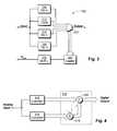
- FIG. 1shows the preferred embodiment of a converter topology 100 according to the invention.
- An analog input signalis applied to the input of a track-and-hold circuit 120 .
- the track-and-hold circuit 120has an output coupled to respective inputs of a plurality of ADC stages 110 a - 110 k .
- Each ADC stagegenerates a digital output signal that corresponds to the analog signal applied to its input.
- the ADC stages 110 a - 110 kpreferably operate from a common clock (not shown), which causes them to perform their conversions substantially simultaneously.
- the track-and-hold circuit 120preferably operates from a time-advanced version of the same clock, which allows the output of the track-and-hold 120 to settle prior to conversions of the ADC stages.
- a combining circuit 116gathers the digital outputs from the ADC stages 110 a - 110 k and sums them together to generate a combined digital output signal.
- each ADC stage 110 a - 110 kalso generates an analog output signal that represents the digital output signal of the respective ADC stage, in analog form.
- the topologyapplies the analog outputs for correcting errors in the digital outputs of the ADC stages.
- a first summer 112adds the analog outputs from the ADC stages 10 a - 10 k .
- a second summer 114subtracts the output of the first summer 112 from the sampled analog input signal, to generate an error signal.
- a fine tune ADC 118converts the error signal into digital form, and a digital summer 122 subtracts the digital error signal from the combined digital output signal to generate a corrected signal, “N-bit Digital Output.”
- FIG. 2shows the preferred embodiment of an ADC stage 110 , which is typical of the ADC stages 110 a - 110 k .
- the ADC stage 110receives an analog input from the track-and-hold circuit 120 , and generates both an analog output and a digital output.
- the ADC stage 110preferably comprises a single loop, multi-bit sigma-delta converter.
- the converterincludes a summer 210 , an ADC 214 , a loop filter 212 , and a DAC (digital-to-analog converter) 218 .
- the ADC 214 and DAC 218are preferably monolithic high-speed 18-bit converters. They are preferably integrated on the same chip to provide substantially identical thermal characteristics and gain.
- the loop filter 212is preferably an integrator.
- the summer 210subtracts the output of the DAC 218 from the analog input signal to produce an error signal.
- the loop filter 212integrates the error signal over time. Negative feedback tends to cause the output of the DAC 218 to equal to the analog input of the ADC stage. In so doing, the negative feedback tends to drive the output of the ADC 214 to a value that precisely corresponds to a digital representation of the ADC stage's analog input.
- sigma-delta loopsprovide inherent noise shaping. Although the resolution of the converters 214 and 218 may be limited to 18 bits, the precision of the loop over time greatly exceeds 18 bits due to the tendency of the negative feedback to drive the average of the output to the precise value of the analog input. Although the feedback loop generally requires several samples to settle, the loop still settles quickly due to the high sampling rate. Therefore, the multi-bit sigma-delta loop greatly improves precision without unduly impacting speed.
- FIG. 3shows the preferred implementation of the track-and-hold circuit 120 .
- the track-and-hold circuit 120includes a plurality of individual track-and-holds ( 310 , 312 , 314 , 316 ) having inputs connected together and outputs connected to different inputs of a multiplexor 322 .
- a counter 320is coupled to control inputs of the multiplexor 322 for selecting an input for passage to the output of the multiplexor 322 .
- a phase-locked loop 318receives a clock signal FCLK and multiplies its frequency. The multiplied clock drives the counter 320 , which, in turn, causes the multiplexor 322 to repetitively cycle through its inputs at the multiplied rate.
- FCLKclock signal
- FCLKmultiplies its frequency
- the multiplied clockdrives the counter 320 , which, in turn, causes the multiplexor 322 to repetitively cycle through its inputs at the multiplied rate.
- the precision of the topology 100can be increased even further using the configuration of FIG. 4 .
- the analog input signalis conveyed through first and second circuit branches including analog-to-digital converters 414 and 416 , respectively.
- the converters 414 and 416are substantially identical to the converter topology 100 of FIG. 1 .
- An adder 410receives the digital outputs of the converters 414 and 416 .
- the adder 410subtracts the digital output of the second converter from the digital output of the first converter to produce an output signal proportional to the noise in the input signal. This noise is then subtracted from the digital output of the first converter 412 , to produce an enhanced output signal, “Digital Output”.
- the topology 100can be somewhat simplified if it is used in the configuration of FIG. 4 .
- a single track-and-hold circuit 120can be used for sampling the analog input signal for both converters 414 and 416 , rather than requiring a separate track-and-hold for each.
- the operations of the combining circuits 116 and digital summers 122can be incorporated into functionality of the adder 410 , rather than being provided as separate structures.
- the adder 410is preferably implemented in software using a standard Digital Signal Processing engine. Alternatively, it can be implemented in hardware using dedicated digital circuitry or other circuits, the specific form of which is not critical to the invention.
- Multi-bit sigma-delta loopscan be implemented in a wide variety of ways known to those skilled in the art.
- the loop filter 212can be implemented as an analog control amplifier, such as an integrator, which precedes rather than follows the ADC 214 .
- This and other variations of the sigma-delta loopcan be used, as applications require, within the scope of the invention.
Landscapes
- Engineering & Computer Science (AREA)
- Theoretical Computer Science (AREA)
- Compression, Expansion, Code Conversion, And Decoders (AREA)
Abstract
Description
Claims (20)
Priority Applications (1)
| Application Number | Priority Date | Filing Date | Title |
|---|---|---|---|
| US10/016,983US6683550B2 (en) | 2001-12-14 | 2001-12-14 | High precision, high-speed signal capture |
Applications Claiming Priority (1)
| Application Number | Priority Date | Filing Date | Title |
|---|---|---|---|
| US10/016,983US6683550B2 (en) | 2001-12-14 | 2001-12-14 | High precision, high-speed signal capture |
Publications (2)
| Publication Number | Publication Date |
|---|---|
| US20030112165A1 US20030112165A1 (en) | 2003-06-19 |
| US6683550B2true US6683550B2 (en) | 2004-01-27 |
Family
ID=21780077
Family Applications (1)
| Application Number | Title | Priority Date | Filing Date |
|---|---|---|---|
| US10/016,983Expired - Fee RelatedUS6683550B2 (en) | 2001-12-14 | 2001-12-14 | High precision, high-speed signal capture |
Country Status (1)
| Country | Link |
|---|---|
| US (1) | US6683550B2 (en) |
Cited By (25)
| Publication number | Priority date | Publication date | Assignee | Title |
|---|---|---|---|---|
| US20030078103A1 (en)* | 2001-09-28 | 2003-04-24 | Igt | Game development architecture that decouples the game logic from the graphics logic |
| US20030203755A1 (en)* | 2002-04-25 | 2003-10-30 | Shuffle Master, Inc. | Encryption in a secure computerized gaming system |
| US20040189499A1 (en)* | 2003-03-28 | 2004-09-30 | Ho-San Han | Sigma delta beamformer and method with reduced artifact |
| US20050192092A1 (en)* | 2001-09-28 | 2005-09-01 | Igt | Decoupling of the graphical presentation of a game from the presentation logic |
| US20050219107A1 (en)* | 2004-03-25 | 2005-10-06 | Guidry David W | System and method for successive approximation |
| US20060208935A1 (en)* | 2005-03-21 | 2006-09-21 | Analog Devices, Inc. | Analog to digital converter |
| US20060208937A1 (en)* | 2005-03-21 | 2006-09-21 | Analog Devices, Inc. | Analog to digital converter |
| US20070015590A1 (en)* | 2000-03-08 | 2007-01-18 | Igt | Encryption in a secure computerized gaming system |
| US20070035431A1 (en)* | 2005-08-12 | 2007-02-15 | Analog Devices, Inc. | Analog to digital converter |
| US7289054B1 (en)* | 2006-06-13 | 2007-10-30 | Toyota Jidosha Kabushiki Kaisha | Parallel oversampling algorithmic A/D converter and method of using the same |
| US20080102919A1 (en)* | 2001-09-28 | 2008-05-01 | Igt | Pluggable modular gaming modifiers and configuration templates for gaming environments |
| US20090135038A1 (en)* | 2007-11-28 | 2009-05-28 | Abhijit Kumar Das | Sigma Delta Modulator Summing Input, Reference Voltage, And Feedback |
| WO2010151851A1 (en) | 2009-06-26 | 2010-12-29 | Syntropy Systems | Sampling/quantization converters |
| US20110095927A1 (en)* | 2009-06-26 | 2011-04-28 | Syntropy Systems, Llc | Sampling/Quantization Converters |
| US20110163900A1 (en)* | 2010-01-05 | 2011-07-07 | Syntropy Systems, Llc | Multimode Sampling/Quantization Converters |
| WO2012106395A1 (en) | 2011-02-04 | 2012-08-09 | Syntropy Systems | Sampling/quantization converters |
| US8917198B2 (en) | 2010-01-05 | 2014-12-23 | Syntropy Systems, Llc | Multi-mode sampling/quantization converters |
| US8943112B2 (en) | 2009-06-26 | 2015-01-27 | Syntropy Systems, Llc | Sampling/quantization converters |
| US9130584B1 (en) | 2010-01-05 | 2015-09-08 | Syntropy Systems, Llc | Multi-mode sampling/quantization converters |
| US9209829B2 (en) | 2009-06-26 | 2015-12-08 | Syntropy Systems, Llc | Sampling/quantization converters |
| US9350373B1 (en)* | 2014-12-17 | 2016-05-24 | Mediatek Inc. | Analog-to-digital converter and long-term-evolution advanced device and method for analog-to-digital conversion |
| US9419637B1 (en) | 2010-01-05 | 2016-08-16 | Syntropy Systems, Llc | Multi-mode sampling/quantization converters |
| US9621175B2 (en) | 2015-02-11 | 2017-04-11 | Syntropy Systems, Llc | Sampling/quantization converters |
| US9654128B2 (en) | 2010-01-05 | 2017-05-16 | Syntropy Systems, Llc | Multi-mode sampling/quantization converters |
| US9680498B2 (en) | 2009-06-26 | 2017-06-13 | Syntropy Systems, Llc | Sampling/quantization converters |
Families Citing this family (2)
| Publication number | Priority date | Publication date | Assignee | Title |
|---|---|---|---|---|
| US6873280B2 (en)* | 2003-06-12 | 2005-03-29 | Northrop Grumman Corporation | Conversion employing delta-sigma modulation |
| JP5892162B2 (en)* | 2011-05-10 | 2016-03-23 | 日本電気株式会社 | Digital modulator |
Citations (9)
| Publication number | Priority date | Publication date | Assignee | Title |
|---|---|---|---|---|
| US4131885A (en) | 1975-05-01 | 1978-12-26 | Sony Corporation | Parallel-serial analog to digital converters |
| US5073777A (en)* | 1989-03-13 | 1991-12-17 | Texas Instruments Incorporated | Plural delta-sigma converters operating in parallel with independent dither generators |
| US5150120A (en) | 1991-01-03 | 1992-09-22 | Harris Corp. | Multiplexed sigma-delta A/D converter |
| US5196852A (en) | 1992-02-21 | 1993-03-23 | California Institute Of Technology | Analog-to-digital converter using parallel ΔΣ modulators |
| US5363101A (en)* | 1992-09-07 | 1994-11-08 | Sony Corporation | Analog to digital converter |
| US5835044A (en)* | 1996-04-23 | 1998-11-10 | Sony Corporation | 1-Bit A/D converting device with reduced noise component |
| US5896100A (en) | 1994-09-30 | 1999-04-20 | Cennoid Technologies, Inc. | Method and apparatus for analog-to-digital or digital-to-analog conversion |
| US6195031B1 (en) | 1998-12-28 | 2001-02-27 | Siemens Aktiengesellschaft | Analog-to-digital converter with level converter and level recognition unit and correction memory |
| US6195032B1 (en) | 1999-08-12 | 2001-02-27 | Centillium Communications, Inc. | Two-stage pipelined recycling analog-to-digital converter (ADC) |
- 2001
- 2001-12-14USUS10/016,983patent/US6683550B2/ennot_activeExpired - Fee Related
Patent Citations (9)
| Publication number | Priority date | Publication date | Assignee | Title |
|---|---|---|---|---|
| US4131885A (en) | 1975-05-01 | 1978-12-26 | Sony Corporation | Parallel-serial analog to digital converters |
| US5073777A (en)* | 1989-03-13 | 1991-12-17 | Texas Instruments Incorporated | Plural delta-sigma converters operating in parallel with independent dither generators |
| US5150120A (en) | 1991-01-03 | 1992-09-22 | Harris Corp. | Multiplexed sigma-delta A/D converter |
| US5196852A (en) | 1992-02-21 | 1993-03-23 | California Institute Of Technology | Analog-to-digital converter using parallel ΔΣ modulators |
| US5363101A (en)* | 1992-09-07 | 1994-11-08 | Sony Corporation | Analog to digital converter |
| US5896100A (en) | 1994-09-30 | 1999-04-20 | Cennoid Technologies, Inc. | Method and apparatus for analog-to-digital or digital-to-analog conversion |
| US5835044A (en)* | 1996-04-23 | 1998-11-10 | Sony Corporation | 1-Bit A/D converting device with reduced noise component |
| US6195031B1 (en) | 1998-12-28 | 2001-02-27 | Siemens Aktiengesellschaft | Analog-to-digital converter with level converter and level recognition unit and correction memory |
| US6195032B1 (en) | 1999-08-12 | 2001-02-27 | Centillium Communications, Inc. | Two-stage pipelined recycling analog-to-digital converter (ADC) |
Non-Patent Citations (3)
| Title |
|---|
| Cascaded parallel oversampling sigma-delta modulators Xuesheng Wang; Wei Qin; Xieting Ling Circuits and Systems II: Analog and Digital Signal Processing, IEEE Transactions on , vol. 47 Issue: 2, Feb. 2000, Page(s): 156-161. |
| Effects of quantization noise in parallel arrays of analog-to-digital converters Petraglia, A.; Pinheiro, M.A.A. Circuits and Systems, 1994. ISCAS '94., 1994 IEEE International Symposium on , vol.: 5 , 1994 , Page(s): 337-340 vol. 5. |
| Oversampling parallel delta-sigma modulator A/D conversion Galton I.; Jensen, H.T. Circuits and Systems II: Analog and Digital Signal Processing, IEEE Transactions on , vol.: 43 Issue: 12 , Dec. 1996 , Page(s): 801-810. |
Cited By (38)
| Publication number | Priority date | Publication date | Assignee | Title |
|---|---|---|---|---|
| US20070015590A1 (en)* | 2000-03-08 | 2007-01-18 | Igt | Encryption in a secure computerized gaming system |
| US20050192092A1 (en)* | 2001-09-28 | 2005-09-01 | Igt | Decoupling of the graphical presentation of a game from the presentation logic |
| US20080102919A1 (en)* | 2001-09-28 | 2008-05-01 | Igt | Pluggable modular gaming modifiers and configuration templates for gaming environments |
| US20080058055A1 (en)* | 2001-09-28 | 2008-03-06 | Igt | Game development architecture that decouples the game logic from the graphics logic |
| US20030078103A1 (en)* | 2001-09-28 | 2003-04-24 | Igt | Game development architecture that decouples the game logic from the graphics logic |
| US20030203755A1 (en)* | 2002-04-25 | 2003-10-30 | Shuffle Master, Inc. | Encryption in a secure computerized gaming system |
| US7199738B2 (en)* | 2003-03-28 | 2007-04-03 | Siemens Medical Solutions Usa, Inc. | Sigma delta beamformer and method with reduced artifact |
| US20040189499A1 (en)* | 2003-03-28 | 2004-09-30 | Ho-San Han | Sigma delta beamformer and method with reduced artifact |
| US7265694B2 (en)* | 2004-03-25 | 2007-09-04 | Texas Instruments Incorporated | System and method for successive approximation |
| US20050219107A1 (en)* | 2004-03-25 | 2005-10-06 | Guidry David W | System and method for successive approximation |
| US7250880B2 (en)* | 2005-03-21 | 2007-07-31 | Analog Devices, Inc. | Analog to digital converter |
| US20060208937A1 (en)* | 2005-03-21 | 2006-09-21 | Analog Devices, Inc. | Analog to digital converter |
| US7274321B2 (en)* | 2005-03-21 | 2007-09-25 | Analog Devices, Inc. | Analog to digital converter |
| US20060208935A1 (en)* | 2005-03-21 | 2006-09-21 | Analog Devices, Inc. | Analog to digital converter |
| US20070035431A1 (en)* | 2005-08-12 | 2007-02-15 | Analog Devices, Inc. | Analog to digital converter |
| US7218259B2 (en) | 2005-08-12 | 2007-05-15 | Analog Devices, Inc. | Analog-to-digital converter with signal-to-noise ratio enhancement |
| US7289054B1 (en)* | 2006-06-13 | 2007-10-30 | Toyota Jidosha Kabushiki Kaisha | Parallel oversampling algorithmic A/D converter and method of using the same |
| US7564391B2 (en)* | 2007-11-28 | 2009-07-21 | Texas Instruments Incorporated | Sigma delta modulator summing input, reference voltage, and feedback |
| US20090135038A1 (en)* | 2007-11-28 | 2009-05-28 | Abhijit Kumar Das | Sigma Delta Modulator Summing Input, Reference Voltage, And Feedback |
| US8604957B2 (en) | 2009-06-26 | 2013-12-10 | Syntropy Systems, Llc | Sampling/quantization converters |
| WO2010151851A1 (en) | 2009-06-26 | 2010-12-29 | Syntropy Systems | Sampling/quantization converters |
| US20100328125A1 (en)* | 2009-06-26 | 2010-12-30 | Syntropy Systems, Llc | Sampling/Quantization Converters |
| US20110095927A1 (en)* | 2009-06-26 | 2011-04-28 | Syntropy Systems, Llc | Sampling/Quantization Converters |
| US9680498B2 (en) | 2009-06-26 | 2017-06-13 | Syntropy Systems, Llc | Sampling/quantization converters |
| US8089382B2 (en) | 2009-06-26 | 2012-01-03 | Syntropy Systems, Llc | Sampling/quantization converters |
| US9209829B2 (en) | 2009-06-26 | 2015-12-08 | Syntropy Systems, Llc | Sampling/quantization converters |
| US8299947B2 (en) | 2009-06-26 | 2012-10-30 | Syntropy Systems, Llc | Sampling/quantization converters |
| US8943112B2 (en) | 2009-06-26 | 2015-01-27 | Syntropy Systems, Llc | Sampling/quantization converters |
| WO2011085042A1 (en) | 2010-01-05 | 2011-07-14 | Syntropy Systems | Sampling/quantization converters |
| US8917198B2 (en) | 2010-01-05 | 2014-12-23 | Syntropy Systems, Llc | Multi-mode sampling/quantization converters |
| US8416111B2 (en) | 2010-01-05 | 2013-04-09 | Sytropy Systems, LLC | Multimode sampling/quantization converters |
| US9130584B1 (en) | 2010-01-05 | 2015-09-08 | Syntropy Systems, Llc | Multi-mode sampling/quantization converters |
| US9419637B1 (en) | 2010-01-05 | 2016-08-16 | Syntropy Systems, Llc | Multi-mode sampling/quantization converters |
| US9654128B2 (en) | 2010-01-05 | 2017-05-16 | Syntropy Systems, Llc | Multi-mode sampling/quantization converters |
| US20110163900A1 (en)* | 2010-01-05 | 2011-07-07 | Syntropy Systems, Llc | Multimode Sampling/Quantization Converters |
| WO2012106395A1 (en) | 2011-02-04 | 2012-08-09 | Syntropy Systems | Sampling/quantization converters |
| US9350373B1 (en)* | 2014-12-17 | 2016-05-24 | Mediatek Inc. | Analog-to-digital converter and long-term-evolution advanced device and method for analog-to-digital conversion |
| US9621175B2 (en) | 2015-02-11 | 2017-04-11 | Syntropy Systems, Llc | Sampling/quantization converters |
Also Published As
| Publication number | Publication date |
|---|---|
| US20030112165A1 (en) | 2003-06-19 |
Similar Documents
| Publication | Publication Date | Title |
|---|---|---|
| US6683550B2 (en) | High precision, high-speed signal capture | |
| US6124818A (en) | Pipelined successive approximation analog-to-digital converters | |
| CN109586720B (en) | Analog-to-digital converter and working method thereof | |
| US6184809B1 (en) | User transparent self-calibration technique for pipelined ADC architecture | |
| US6975682B2 (en) | Multi-bit delta-sigma analog-to-digital converter with error shaping | |
| US6617992B2 (en) | Capacitor mismatch independent gain stage for differential pipeline analog to digital converters | |
| US6970118B2 (en) | High-speed high-resolution ADC for precision measurements | |
| US5973631A (en) | Test circuit and method of trimming a unary digital-to-analog converter (DAC) in a subranging analog-to-digital converter (ADC) | |
| US7443332B2 (en) | Time continuous pipeline analog-to-digital converter | |
| US7414562B2 (en) | Analog-to-digital conversion using asynchronous current-mode cyclic comparison | |
| US20030058149A1 (en) | Analog to digital converter | |
| JPH03190430A (en) | analog to digital converter | |
| US11424754B1 (en) | Noise-shaping analog-to-digital converter | |
| US6285309B1 (en) | Nested pipelined analog-to-digital converter | |
| CN110995268B (en) | Multi-order successive approximation type n bit analog-to-digital converter | |
| JP2004500727A (en) | Recursive multi-bit analog-to-digital converter with predictor | |
| US6762707B2 (en) | Programmable architecture analog-to-digital converter | |
| US6603418B2 (en) | High precision, high-speed signal source | |
| JP7621059B2 (en) | Digital-to-analog converter, source measure unit and method for converting a digital signal to an analog signal | |
| KR100294787B1 (en) | Sub-ranging analog-to-digital converter with open-loop differential amplifiers | |
| US4855745A (en) | High resolution analog-to-digital converter | |
| US7187317B2 (en) | A/D conversion apparatus | |
| US5084701A (en) | Digital-to-analog converter using cyclical current source switching | |
| US6300892B2 (en) | Linearized multibit digital/analog converter and its use in a multibit delta-sigma analog/digital converter | |
| Bruce | Nyquist-rate digital-to-analog converter architectures |
Legal Events
| Date | Code | Title | Description |
|---|---|---|---|
| AS | Assignment | Owner name:TERADYNE, INC., MASSACHUSETTS Free format text:ASSIGNMENT OF ASSIGNORS INTEREST;ASSIGNOR:AL-AWADHI, AYMAN A.;REEL/FRAME:012401/0214 Effective date:20011214 | |
| FPAY | Fee payment | Year of fee payment:4 | |
| AS | Assignment | Owner name:BANK OF AMERICA, N.A., AS ADMINISTRATIVE AGENT, TE Free format text:NOTICE OF GRANT OF SECURITY INTEREST IN PATENTS;ASSIGNOR:TERADYNE, INC.;REEL/FRAME:021912/0762 Effective date:20081114 Owner name:BANK OF AMERICA, N.A., AS ADMINISTRATIVE AGENT,TEX Free format text:NOTICE OF GRANT OF SECURITY INTEREST IN PATENTS;ASSIGNOR:TERADYNE, INC.;REEL/FRAME:021912/0762 Effective date:20081114 | |
| AS | Assignment | Owner name:TERADYNE, INC, MASSACHUSETTS Free format text:RELEASE BY SECURED PARTY;ASSIGNOR:BANK OF AMERICA, N.A.;REEL/FRAME:022668/0750 Effective date:20090427 Owner name:TERADYNE, INC,MASSACHUSETTS Free format text:RELEASE BY SECURED PARTY;ASSIGNOR:BANK OF AMERICA, N.A.;REEL/FRAME:022668/0750 Effective date:20090427 | |
| FPAY | Fee payment | Year of fee payment:8 | |
| AS | Assignment | Owner name:BARCLAYS BANK PLC, NEW YORK Free format text:PATENT SECURITY AGREEMENT;ASSIGNORS:TERADYNE, INC.;LITEPOINT CORPORATION;REEL/FRAME:035507/0116 Effective date:20150427 | |
| REMI | Maintenance fee reminder mailed | ||
| LAPS | Lapse for failure to pay maintenance fees | ||
| STCH | Information on status: patent discontinuation | Free format text:PATENT EXPIRED DUE TO NONPAYMENT OF MAINTENANCE FEES UNDER 37 CFR 1.362 | |
| FP | Lapsed due to failure to pay maintenance fee | Effective date:20160127 | |
| AS | Assignment | Owner name:TERADYNE, INC., MASSACHUSETTS Free format text:RELEASE OF SECURITY INTEREST IN INTELLECTUAL PROPERTY;ASSIGNOR:BARCLAYS BANK PLC, AS COLLATERAL AGENT;REEL/FRAME:049632/0940 Effective date:20190627 Owner name:LITEPOINT CORPORATION, CALIFORNIA Free format text:RELEASE OF SECURITY INTEREST IN INTELLECTUAL PROPERTY;ASSIGNOR:BARCLAYS BANK PLC, AS COLLATERAL AGENT;REEL/FRAME:049632/0940 Effective date:20190627 Owner name:GENRAD, LLC, MASSACHUSETTS Free format text:RELEASE OF SECURITY INTEREST IN INTELLECTUAL PROPERTY;ASSIGNOR:BARCLAYS BANK PLC, AS COLLATERAL AGENT;REEL/FRAME:049632/0940 Effective date:20190627 Owner name:EAGLE TEST SYSTEMS, INC., ILLINOIS Free format text:RELEASE OF SECURITY INTEREST IN INTELLECTUAL PROPERTY;ASSIGNOR:BARCLAYS BANK PLC, AS COLLATERAL AGENT;REEL/FRAME:049632/0940 Effective date:20190627 Owner name:NEXTEST SYSTEMS CORPORATION, CALIFORNIA Free format text:RELEASE OF SECURITY INTEREST IN INTELLECTUAL PROPERTY;ASSIGNOR:BARCLAYS BANK PLC, AS COLLATERAL AGENT;REEL/FRAME:049632/0940 Effective date:20190627 Owner name:ENERGID TECHNOLOGIES CORPORATION, MASSACHUSETTS Free format text:RELEASE OF SECURITY INTEREST IN INTELLECTUAL PROPERTY;ASSIGNOR:BARCLAYS BANK PLC, AS COLLATERAL AGENT;REEL/FRAME:049632/0940 Effective date:20190627 |