US6683274B1 - Wafer susceptor - Google Patents
Wafer susceptorDownload PDFInfo
- Publication number
- US6683274B1 US6683274B1US10/295,954US29595402AUS6683274B1US 6683274 B1US6683274 B1US 6683274B1US 29595402 AUS29595402 AUS 29595402AUS 6683274 B1US6683274 B1US 6683274B1
- Authority
- US
- United States
- Prior art keywords
- shield
- electrode
- heater
- ceramic body
- susceptor
- Prior art date
- Legal status (The legal status is an assumption and is not a legal conclusion. Google has not performed a legal analysis and makes no representation as to the accuracy of the status listed.)
- Expired - Lifetime
Links
- 239000000919ceramicSubstances0.000claimsabstractdescription36
- 239000010409thin filmSubstances0.000claimsabstractdescription18
- 239000007769metal materialSubstances0.000claimsabstractdescription3
- 229910052751metalInorganic materials0.000claimsdescription16
- 239000002184metalSubstances0.000claimsdescription16
- ZOKXTWBITQBERF-UHFFFAOYSA-NMolybdenumChemical compound[Mo]ZOKXTWBITQBERF-UHFFFAOYSA-N0.000claimsdescription2
- PNEYBMLMFCGWSK-UHFFFAOYSA-Naluminium oxideInorganic materials[O-2].[O-2].[O-2].[Al+3].[Al+3]PNEYBMLMFCGWSK-UHFFFAOYSA-N0.000claimsdescription2
- 229910052593corundumInorganic materials0.000claimsdescription2
- 229910052750molybdenumInorganic materials0.000claimsdescription2
- 239000011733molybdenumSubstances0.000claimsdescription2
- WFKWXMTUELFFGS-UHFFFAOYSA-NtungstenChemical compound[W]WFKWXMTUELFFGS-UHFFFAOYSA-N0.000claimsdescription2
- 229910052721tungstenInorganic materials0.000claimsdescription2
- 239000010937tungstenSubstances0.000claimsdescription2
- 229910001845yogo sapphireInorganic materials0.000claimsdescription2
- 238000010438heat treatmentMethods0.000abstractdescription3
- 230000006641stabilisationEffects0.000abstract1
- 238000011105stabilizationMethods0.000abstract1
- 238000000623plasma-assisted chemical vapour depositionMethods0.000description6
- 238000000034methodMethods0.000description4
- 238000006243chemical reactionMethods0.000description3
- 238000005229chemical vapour depositionMethods0.000description3
- 239000011248coating agentSubstances0.000description3
- 238000000576coating methodMethods0.000description3
- 230000008878couplingEffects0.000description2
- 238000010168coupling processMethods0.000description2
- 238000005859coupling reactionMethods0.000description2
- 239000010408filmSubstances0.000description2
- 230000004075alterationEffects0.000description1
- 230000009977dual effectEffects0.000description1
- 230000000694effectsEffects0.000description1
- 230000005684electric fieldEffects0.000description1
- 150000002500ionsChemical class0.000description1
- 238000004519manufacturing processMethods0.000description1
- 230000002093peripheral effectEffects0.000description1
- 239000004065semiconductorSubstances0.000description1
- 238000006467substitution reactionMethods0.000description1
- 230000003313weakening effectEffects0.000description1
Images


Classifications
- H—ELECTRICITY
- H01—ELECTRIC ELEMENTS
- H01L—SEMICONDUCTOR DEVICES NOT COVERED BY CLASS H10
- H01L21/00—Processes or apparatus adapted for the manufacture or treatment of semiconductor or solid state devices or of parts thereof
- H01L21/02—Manufacture or treatment of semiconductor devices or of parts thereof
- H01L21/04—Manufacture or treatment of semiconductor devices or of parts thereof the devices having potential barriers, e.g. a PN junction, depletion layer or carrier concentration layer
- H01L21/18—Manufacture or treatment of semiconductor devices or of parts thereof the devices having potential barriers, e.g. a PN junction, depletion layer or carrier concentration layer the devices having semiconductor bodies comprising elements of Group IV of the Periodic Table or AIIIBV compounds with or without impurities, e.g. doping materials
- H01L21/20—Deposition of semiconductor materials on a substrate, e.g. epitaxial growth solid phase epitaxy
- H—ELECTRICITY
- H01—ELECTRIC ELEMENTS
- H01L—SEMICONDUCTOR DEVICES NOT COVERED BY CLASS H10
- H01L21/00—Processes or apparatus adapted for the manufacture or treatment of semiconductor or solid state devices or of parts thereof
- H01L21/67—Apparatus specially adapted for handling semiconductor or electric solid state devices during manufacture or treatment thereof; Apparatus specially adapted for handling wafers during manufacture or treatment of semiconductor or electric solid state devices or components ; Apparatus not specifically provided for elsewhere
- H01L21/67005—Apparatus not specifically provided for elsewhere
- H01L21/67011—Apparatus for manufacture or treatment
- H01L21/67098—Apparatus for thermal treatment
- H01L21/67103—Apparatus for thermal treatment mainly by conduction
- C—CHEMISTRY; METALLURGY
- C23—COATING METALLIC MATERIAL; COATING MATERIAL WITH METALLIC MATERIAL; CHEMICAL SURFACE TREATMENT; DIFFUSION TREATMENT OF METALLIC MATERIAL; COATING BY VACUUM EVAPORATION, BY SPUTTERING, BY ION IMPLANTATION OR BY CHEMICAL VAPOUR DEPOSITION, IN GENERAL; INHIBITING CORROSION OF METALLIC MATERIAL OR INCRUSTATION IN GENERAL
- C23C—COATING METALLIC MATERIAL; COATING MATERIAL WITH METALLIC MATERIAL; SURFACE TREATMENT OF METALLIC MATERIAL BY DIFFUSION INTO THE SURFACE, BY CHEMICAL CONVERSION OR SUBSTITUTION; COATING BY VACUUM EVAPORATION, BY SPUTTERING, BY ION IMPLANTATION OR BY CHEMICAL VAPOUR DEPOSITION, IN GENERAL
- C23C16/00—Chemical coating by decomposition of gaseous compounds, without leaving reaction products of surface material in the coating, i.e. chemical vapour deposition [CVD] processes
- C23C16/44—Chemical coating by decomposition of gaseous compounds, without leaving reaction products of surface material in the coating, i.e. chemical vapour deposition [CVD] processes characterised by the method of coating
- C23C16/458—Chemical coating by decomposition of gaseous compounds, without leaving reaction products of surface material in the coating, i.e. chemical vapour deposition [CVD] processes characterised by the method of coating characterised by the method used for supporting substrates in the reaction chamber
- C23C16/4582—Rigid and flat substrates, e.g. plates or discs
- C23C16/4583—Rigid and flat substrates, e.g. plates or discs the substrate being supported substantially horizontally
- C23C16/4586—Elements in the interior of the support, e.g. electrodes, heating or cooling devices
- C—CHEMISTRY; METALLURGY
- C23—COATING METALLIC MATERIAL; COATING MATERIAL WITH METALLIC MATERIAL; CHEMICAL SURFACE TREATMENT; DIFFUSION TREATMENT OF METALLIC MATERIAL; COATING BY VACUUM EVAPORATION, BY SPUTTERING, BY ION IMPLANTATION OR BY CHEMICAL VAPOUR DEPOSITION, IN GENERAL; INHIBITING CORROSION OF METALLIC MATERIAL OR INCRUSTATION IN GENERAL
- C23C—COATING METALLIC MATERIAL; COATING MATERIAL WITH METALLIC MATERIAL; SURFACE TREATMENT OF METALLIC MATERIAL BY DIFFUSION INTO THE SURFACE, BY CHEMICAL CONVERSION OR SUBSTITUTION; COATING BY VACUUM EVAPORATION, BY SPUTTERING, BY ION IMPLANTATION OR BY CHEMICAL VAPOUR DEPOSITION, IN GENERAL
- C23C16/00—Chemical coating by decomposition of gaseous compounds, without leaving reaction products of surface material in the coating, i.e. chemical vapour deposition [CVD] processes
- C23C16/44—Chemical coating by decomposition of gaseous compounds, without leaving reaction products of surface material in the coating, i.e. chemical vapour deposition [CVD] processes characterised by the method of coating
- C23C16/50—Chemical coating by decomposition of gaseous compounds, without leaving reaction products of surface material in the coating, i.e. chemical vapour deposition [CVD] processes characterised by the method of coating using electric discharges
- C23C16/505—Chemical coating by decomposition of gaseous compounds, without leaving reaction products of surface material in the coating, i.e. chemical vapour deposition [CVD] processes characterised by the method of coating using electric discharges using radio frequency discharges
- H—ELECTRICITY
- H01—ELECTRIC ELEMENTS
- H01J—ELECTRIC DISCHARGE TUBES OR DISCHARGE LAMPS
- H01J37/00—Discharge tubes with provision for introducing objects or material to be exposed to the discharge, e.g. for the purpose of examination or processing thereof
- H01J37/32—Gas-filled discharge tubes
- H01J37/32009—Arrangements for generation of plasma specially adapted for examination or treatment of objects, e.g. plasma sources
- H01J37/32082—Radio frequency generated discharge
Definitions
- the present inventionrelates to a wafer susceptor, and more particularly, to a wafer susceptor capable of functioning as the RF electrode and the heater.
- PECVDplasma enhanced chemical vapor deposition
- CVDchemical vapor deposition
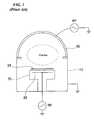
- FIG. 1is a schematic view of a typical PECVD apparatus.
- a susceptor 70 on which a wafer 25 is disposedis mounted within a reaction chamber 10 and an upper RF electrode 30 is mounted on an upper portion of the reaction chamber 10 .
- a lower electrodei.e., the susceptor 70
- the upper electrodeis a plate-shaped electrode or a dome-shaped electrode and an RF power is applied to the upper electrode.
- the RF powermay be applied to the lower electrode (i.e., the susceptor).
- the RF poweris applied to the upper RF electrode 30 , a plasma is generated within the reaction chamber 10 . If the plasma is generated, positive ions existing within the plasma are attracted toward the wafer 25 due to a self-bias, so that a thin film is deposited on the wafer 25 .
- the susceptoris grounded.
- the lower RF electrode 22is mounted within the susceptor 70 and the RF power is also applied to the lower RF electrode 22 . Further, a stress level of the thin film deposited on the wafer 25 can be controlled by applying the RF power to the lower RF electrode 22 . Furthermore, it is possible to protect patterns formed on the wafer from being damaged due to the plasma. This is because the RF power removes charges which are accumulated between the patterns.
- a heater(not shown) is mounted within the susceptor 70 for the purpose of the heating process.
- the heateris affected by an RF noise so that a reliable thin film is not formed. This is because an efficiency of the plasma may be degraded and a system for controlling a temperature of the heater may be also affected.
- the present inventionhas been devised to solve the above problems, and it is an object of the present invention to provide a wafer susceptor functioning as the RF electrode and the heater, thereby capable of minimizing an influence of RF noise on the heater.
- a wafer susceptorcomprising: a ceramic body; an RF electrode mounted within the ceramic body; a heater mounted within the ceramic body and spaced apart from the RF electrode by a predetermined distance to be disposed below the RF electrode; and an RF shield of a metal material, the RF shield being electrically grounded and mounted within the ceramic body, the RF shield being disposed between the RF electrode and the heater without being in contact with either the heater or the RF electrode.
- the RF shieldcan be formed using a metal plate, a net or a thin film coated on the ceramic body.
- FIG. 1is a schematic view of a typical PECVD apparatus
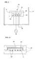
- FIG. 2is a schematic view of a wafer susceptor in accordance with an embodiment of the present invention.
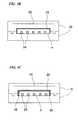
- FIGS. 3A to 3 Dare views showing various embodiments of the susceptor in accordance with the present invention.
- FIG. 2is a schematic view of a wafer susceptor in accordance with an embodiment of the present invention.
- a susceptor 70includes a ceramic body 20 , an RF electrode 22 , a heater 24 and an RF shield 23 .
- the ceramic body 20is formed of AlN or Al 2 O 3 . All of the RF electrode 22 , the heater 24 and the RF shield 23 are mounted within the ceramic body 20 .
- the heater 24is disposed below the RF electrode 22 and spaced apart from the RF electrode 22 by a predetermined distance. Because the heater 24 is not closely in contact with the ceramic body 20 , some space H is formed around the heater 24 . In this embodiment of the present invention, although it is described as an example that some space H is formed around the heater 24 , it is also possible to make a structure having no space around the heater 24 by closely contacting the heater 24 with the ceramic body 20 .
- the RF shield 23acts as a grid electrode for weakening an RF electric field formed between the RF electrode 22 and the heater 24 . Also, the RF shield 23 is mounted between the RF electrode 22 and the heater 24 so that the heater 24 cannot be in contact with the RF electrode 22 .
- the RF shield 23is grounded and formed of a high-temperature resistant metal, such as SUS, molybdenum (Mo) or tungsten (W). Alternatively, the RF shield 23 can be made in a structure that the surroundings of the heater 24 are wound with the RF shield 23 .
- FIGS. 3A to 3 Dare views showing various embodiments of the susceptor 70 , which is characteristic of the present invention.
- FIG. 3Ashows a structure that the RF shield 23 is formed within the ceramic body 20 so that the RF shield 23 can cover the heater 24 .
- the RF shield 23is formed coating a metal thin film on the ceramic body 20 .
- the RF shield 23can be formed in that shape by using a metal plate or a net. In case of the net, it is preferable that each hole size in the net should be 5 or 100 meshes per inch.
- the metal thin filmmay be taken off due to a difference of thermal expansion coefficients between the metal thin film and the ceramic body 20 . Therefore, in order to minimize an undesired influence caused by the difference of the thermal expansion coefficients therebetween, it is desirable that the metal thin film should be formed more thinly, e.g., 0.1 nm to 0.5 mm thick, as possible as can be.
- FIG. 3Bshows a structure the RF shield 23 is mounted in a space H formed between the heater 24 and the ceramic body 20 .
- a lower ceramic bodyis etched and the heater 24 is mounted thereon.
- the resulting structureis covered with an upper ceramic body to thereby form the space H between the heater 24 and the ceramic body 20 .
- the RF shield 23can be easily formed attaching a metal plate or a net on an upper and lateral side of the space H before coupling the upper ceramic body with the upper ceramic body. In another manner, the RF shield 23 can be easily formed coating a metal to thereby form a metal thin film before coupling the lower ceramic body with the upper ceramic body. At this time, it is noted that the RF shield 23 should not be in contact with the heater 24 . Peripheral grooves can be assembled arranging the upper ceramic body and the lower ceramic body, and play a role in preventing an influence on an inner heater caused by a plasma generated from the exterior.
- a ceramic pillar 26is mounted on lateral sides of the space H. Then, the RF shield 23 can be formed disposing a metal plate or a net on the ceramic pillar 26 .
- the RF shield 23covers the heater 24 .
- the RF shield 23is typically formed in a cylinder type.
- the RF shield 23can be formed using a metal plate or a net. Also, in some cases, the RF shield 23 can be formed coating a metal thin film on the ceramic body 20 .
- FIG. 3 D( b )is a perspective view showing a cylinder-type RF shield that uses the net.
- the metal RF shield 23is formed as a grid electrode between the RF electrode 22 and the heater 24 and is grounded, thereby minimizing an influence on the heater 24 , which is caused by an RF noise in case where an RF power is applied to the RF electrode 22 .
- the RF powercan be applied to the susceptor 70 while heating the susceptor 70 at a high temperature, it is possible to deposit a high-density thin film and also control properties of the thin film such as stress and step coverage. Further, the present invention can stabilize a power system of the apparatus.
Landscapes
- Chemical & Material Sciences (AREA)
- Engineering & Computer Science (AREA)
- Physics & Mathematics (AREA)
- Mechanical Engineering (AREA)
- Metallurgy (AREA)
- Plasma & Fusion (AREA)
- Organic Chemistry (AREA)
- Materials Engineering (AREA)
- Chemical Kinetics & Catalysis (AREA)
- General Chemical & Material Sciences (AREA)
- General Physics & Mathematics (AREA)
- Power Engineering (AREA)
- Condensed Matter Physics & Semiconductors (AREA)
- Manufacturing & Machinery (AREA)
- Microelectronics & Electronic Packaging (AREA)
- Computer Hardware Design (AREA)
- Analytical Chemistry (AREA)
- Chemical Vapour Deposition (AREA)
- Container, Conveyance, Adherence, Positioning, Of Wafer (AREA)
Abstract
Description
Claims (8)
Applications Claiming Priority (2)
| Application Number | Priority Date | Filing Date | Title |
|---|---|---|---|
| KR10-2001-0073961 | 2001-11-26 | ||
| KR1020010073961AKR100588774B1 (en) | 2001-11-26 | 2001-11-26 | Wafer susceptor |
Publications (1)
| Publication Number | Publication Date |
|---|---|
| US6683274B1true US6683274B1 (en) | 2004-01-27 |
Family
ID=29571428
Family Applications (1)
| Application Number | Title | Priority Date | Filing Date |
|---|---|---|---|
| US10/295,954Expired - LifetimeUS6683274B1 (en) | 2001-11-26 | 2002-11-18 | Wafer susceptor |
Country Status (3)
| Country | Link |
|---|---|
| US (1) | US6683274B1 (en) |
| KR (1) | KR100588774B1 (en) |
| TW (1) | TWI267161B (en) |
Cited By (275)
| Publication number | Priority date | Publication date | Assignee | Title |
|---|---|---|---|---|
| CN109314039A (en)* | 2016-04-22 | 2019-02-05 | 应用材料公司 | Substrate support pedestal with plasma confinement features |
| KR20200067241A (en) | 2017-01-30 | 2020-06-12 | 엔지케이 인슐레이터 엘티디 | Wafer support table |
| US11001925B2 (en) | 2016-12-19 | 2021-05-11 | Asm Ip Holding B.V. | Substrate processing apparatus |
| US11004977B2 (en) | 2017-07-19 | 2021-05-11 | Asm Ip Holding B.V. | Method for depositing a group IV semiconductor and related semiconductor device structures |
| US11015245B2 (en) | 2014-03-19 | 2021-05-25 | Asm Ip Holding B.V. | Gas-phase reactor and system having exhaust plenum and components thereof |
| US11018002B2 (en) | 2017-07-19 | 2021-05-25 | Asm Ip Holding B.V. | Method for selectively depositing a Group IV semiconductor and related semiconductor device structures |
| US11022879B2 (en) | 2017-11-24 | 2021-06-01 | Asm Ip Holding B.V. | Method of forming an enhanced unexposed photoresist layer |
| US11031242B2 (en) | 2018-11-07 | 2021-06-08 | Asm Ip Holding B.V. | Methods for depositing a boron doped silicon germanium film |
| USD922229S1 (en) | 2019-06-05 | 2021-06-15 | Asm Ip Holding B.V. | Device for controlling a temperature of a gas supply unit |
| US11049751B2 (en) | 2018-09-14 | 2021-06-29 | Asm Ip Holding B.V. | Cassette supply system to store and handle cassettes and processing apparatus equipped therewith |
| US11056344B2 (en) | 2017-08-30 | 2021-07-06 | Asm Ip Holding B.V. | Layer forming method |
| US11053591B2 (en) | 2018-08-06 | 2021-07-06 | Asm Ip Holding B.V. | Multi-port gas injection system and reactor system including same |
| US11069510B2 (en) | 2017-08-30 | 2021-07-20 | Asm Ip Holding B.V. | Substrate processing apparatus |
| US11081345B2 (en) | 2018-02-06 | 2021-08-03 | Asm Ip Holding B.V. | Method of post-deposition treatment for silicon oxide film |
| US11088002B2 (en) | 2018-03-29 | 2021-08-10 | Asm Ip Holding B.V. | Substrate rack and a substrate processing system and method |
| US11087997B2 (en) | 2018-10-31 | 2021-08-10 | Asm Ip Holding B.V. | Substrate processing apparatus for processing substrates |
| US11094546B2 (en) | 2017-10-05 | 2021-08-17 | Asm Ip Holding B.V. | Method for selectively depositing a metallic film on a substrate |
| US11094582B2 (en) | 2016-07-08 | 2021-08-17 | Asm Ip Holding B.V. | Selective deposition method to form air gaps |
| US11101370B2 (en) | 2016-05-02 | 2021-08-24 | Asm Ip Holding B.V. | Method of forming a germanium oxynitride film |
| US11107676B2 (en) | 2016-07-28 | 2021-08-31 | Asm Ip Holding B.V. | Method and apparatus for filling a gap |
| US11114294B2 (en) | 2019-03-08 | 2021-09-07 | Asm Ip Holding B.V. | Structure including SiOC layer and method of forming same |
| US11114283B2 (en) | 2018-03-16 | 2021-09-07 | Asm Ip Holding B.V. | Reactor, system including the reactor, and methods of manufacturing and using same |
| USD930782S1 (en) | 2019-08-22 | 2021-09-14 | Asm Ip Holding B.V. | Gas distributor |
| US11127589B2 (en) | 2019-02-01 | 2021-09-21 | Asm Ip Holding B.V. | Method of topology-selective film formation of silicon oxide |
| US11127617B2 (en) | 2017-11-27 | 2021-09-21 | Asm Ip Holding B.V. | Storage device for storing wafer cassettes for use with a batch furnace |
| USD931978S1 (en) | 2019-06-27 | 2021-09-28 | Asm Ip Holding B.V. | Showerhead vacuum transport |
| US11139191B2 (en) | 2017-08-09 | 2021-10-05 | Asm Ip Holding B.V. | Storage apparatus for storing cassettes for substrates and processing apparatus equipped therewith |
| US11139308B2 (en) | 2015-12-29 | 2021-10-05 | Asm Ip Holding B.V. | Atomic layer deposition of III-V compounds to form V-NAND devices |
| US11158513B2 (en) | 2018-12-13 | 2021-10-26 | Asm Ip Holding B.V. | Methods for forming a rhenium-containing film on a substrate by a cyclical deposition process and related semiconductor device structures |
| US11164955B2 (en) | 2017-07-18 | 2021-11-02 | Asm Ip Holding B.V. | Methods for forming a semiconductor device structure and related semiconductor device structures |
| USD935572S1 (en) | 2019-05-24 | 2021-11-09 | Asm Ip Holding B.V. | Gas channel plate |
| US11171025B2 (en) | 2019-01-22 | 2021-11-09 | Asm Ip Holding B.V. | Substrate processing device |
| US11168395B2 (en) | 2018-06-29 | 2021-11-09 | Asm Ip Holding B.V. | Temperature-controlled flange and reactor system including same |
| US11205585B2 (en) | 2016-07-28 | 2021-12-21 | Asm Ip Holding B.V. | Substrate processing apparatus and method of operating the same |
| US11217444B2 (en) | 2018-11-30 | 2022-01-04 | Asm Ip Holding B.V. | Method for forming an ultraviolet radiation responsive metal oxide-containing film |
| USD940837S1 (en) | 2019-08-22 | 2022-01-11 | Asm Ip Holding B.V. | Electrode |
| US11222772B2 (en) | 2016-12-14 | 2022-01-11 | Asm Ip Holding B.V. | Substrate processing apparatus |
| US11227782B2 (en) | 2019-07-31 | 2022-01-18 | Asm Ip Holding B.V. | Vertical batch furnace assembly |
| US11227789B2 (en) | 2019-02-20 | 2022-01-18 | Asm Ip Holding B.V. | Method and apparatus for filling a recess formed within a substrate surface |
| US11232963B2 (en) | 2018-10-03 | 2022-01-25 | Asm Ip Holding B.V. | Substrate processing apparatus and method |
| US11233133B2 (en) | 2015-10-21 | 2022-01-25 | Asm Ip Holding B.V. | NbMC layers |
| US11230766B2 (en) | 2018-03-29 | 2022-01-25 | Asm Ip Holding B.V. | Substrate processing apparatus and method |
| US11242598B2 (en) | 2015-06-26 | 2022-02-08 | Asm Ip Holding B.V. | Structures including metal carbide material, devices including the structures, and methods of forming same |
| US11244825B2 (en) | 2018-11-16 | 2022-02-08 | Asm Ip Holding B.V. | Methods for depositing a transition metal chalcogenide film on a substrate by a cyclical deposition process |
| US11251040B2 (en) | 2019-02-20 | 2022-02-15 | Asm Ip Holding B.V. | Cyclical deposition method including treatment step and apparatus for same |
| US11251068B2 (en) | 2018-10-19 | 2022-02-15 | Asm Ip Holding B.V. | Substrate processing apparatus and substrate processing method |
| US11251035B2 (en) | 2016-12-22 | 2022-02-15 | Asm Ip Holding B.V. | Method of forming a structure on a substrate |
| USD944946S1 (en) | 2019-06-14 | 2022-03-01 | Asm Ip Holding B.V. | Shower plate |
| US11270899B2 (en) | 2018-06-04 | 2022-03-08 | Asm Ip Holding B.V. | Wafer handling chamber with moisture reduction |
| US11274369B2 (en) | 2018-09-11 | 2022-03-15 | Asm Ip Holding B.V. | Thin film deposition method |
| US11282698B2 (en) | 2019-07-19 | 2022-03-22 | Asm Ip Holding B.V. | Method of forming topology-controlled amorphous carbon polymer film |
| US11289326B2 (en) | 2019-05-07 | 2022-03-29 | Asm Ip Holding B.V. | Method for reforming amorphous carbon polymer film |
| US11286562B2 (en) | 2018-06-08 | 2022-03-29 | Asm Ip Holding B.V. | Gas-phase chemical reactor and method of using same |
| US11286558B2 (en) | 2019-08-23 | 2022-03-29 | Asm Ip Holding B.V. | Methods for depositing a molybdenum nitride film on a surface of a substrate by a cyclical deposition process and related semiconductor device structures including a molybdenum nitride film |
| US11295980B2 (en) | 2017-08-30 | 2022-04-05 | Asm Ip Holding B.V. | Methods for depositing a molybdenum metal film over a dielectric surface of a substrate by a cyclical deposition process and related semiconductor device structures |
| US11296189B2 (en) | 2018-06-21 | 2022-04-05 | Asm Ip Holding B.V. | Method for depositing a phosphorus doped silicon arsenide film and related semiconductor device structures |
| USD947913S1 (en) | 2019-05-17 | 2022-04-05 | Asm Ip Holding B.V. | Susceptor shaft |
| USD948463S1 (en) | 2018-10-24 | 2022-04-12 | Asm Ip Holding B.V. | Susceptor for semiconductor substrate supporting apparatus |
| US11306395B2 (en) | 2017-06-28 | 2022-04-19 | Asm Ip Holding B.V. | Methods for depositing a transition metal nitride film on a substrate by atomic layer deposition and related deposition apparatus |
| USD949319S1 (en) | 2019-08-22 | 2022-04-19 | Asm Ip Holding B.V. | Exhaust duct |
| US11315794B2 (en) | 2019-10-21 | 2022-04-26 | Asm Ip Holding B.V. | Apparatus and methods for selectively etching films |
| US11339476B2 (en) | 2019-10-08 | 2022-05-24 | Asm Ip Holding B.V. | Substrate processing device having connection plates, substrate processing method |
| US11342216B2 (en) | 2019-02-20 | 2022-05-24 | Asm Ip Holding B.V. | Cyclical deposition method and apparatus for filling a recess formed within a substrate surface |
| US11345999B2 (en) | 2019-06-06 | 2022-05-31 | Asm Ip Holding B.V. | Method of using a gas-phase reactor system including analyzing exhausted gas |
| US11355338B2 (en) | 2019-05-10 | 2022-06-07 | Asm Ip Holding B.V. | Method of depositing material onto a surface and structure formed according to the method |
| US11361990B2 (en) | 2018-05-28 | 2022-06-14 | Asm Ip Holding B.V. | Substrate processing method and device manufactured by using the same |
| US11374112B2 (en) | 2017-07-19 | 2022-06-28 | Asm Ip Holding B.V. | Method for depositing a group IV semiconductor and related semiconductor device structures |
| US11378337B2 (en) | 2019-03-28 | 2022-07-05 | Asm Ip Holding B.V. | Door opener and substrate processing apparatus provided therewith |
| US11387106B2 (en) | 2018-02-14 | 2022-07-12 | Asm Ip Holding B.V. | Method for depositing a ruthenium-containing film on a substrate by a cyclical deposition process |
| US11387120B2 (en) | 2017-09-28 | 2022-07-12 | Asm Ip Holding B.V. | Chemical dispensing apparatus and methods for dispensing a chemical to a reaction chamber |
| US11390946B2 (en) | 2019-01-17 | 2022-07-19 | Asm Ip Holding B.V. | Methods of forming a transition metal containing film on a substrate by a cyclical deposition process |
| US11390945B2 (en) | 2019-07-03 | 2022-07-19 | Asm Ip Holding B.V. | Temperature control assembly for substrate processing apparatus and method of using same |
| US11390950B2 (en) | 2017-01-10 | 2022-07-19 | Asm Ip Holding B.V. | Reactor system and method to reduce residue buildup during a film deposition process |
| US11393690B2 (en) | 2018-01-19 | 2022-07-19 | Asm Ip Holding B.V. | Deposition method |
| US11398382B2 (en) | 2018-03-27 | 2022-07-26 | Asm Ip Holding B.V. | Method of forming an electrode on a substrate and a semiconductor device structure including an electrode |
| US11396702B2 (en) | 2016-11-15 | 2022-07-26 | Asm Ip Holding B.V. | Gas supply unit and substrate processing apparatus including the gas supply unit |
| US11401605B2 (en) | 2019-11-26 | 2022-08-02 | Asm Ip Holding B.V. | Substrate processing apparatus |
| US11411088B2 (en) | 2018-11-16 | 2022-08-09 | Asm Ip Holding B.V. | Methods for forming a metal silicate film on a substrate in a reaction chamber and related semiconductor device structures |
| US11410851B2 (en) | 2017-02-15 | 2022-08-09 | Asm Ip Holding B.V. | Methods for forming a metallic film on a substrate by cyclical deposition and related semiconductor device structures |
| US11414760B2 (en) | 2018-10-08 | 2022-08-16 | Asm Ip Holding B.V. | Substrate support unit, thin film deposition apparatus including the same, and substrate processing apparatus including the same |
| US11417545B2 (en) | 2017-08-08 | 2022-08-16 | Asm Ip Holding B.V. | Radiation shield |
| US11424119B2 (en) | 2019-03-08 | 2022-08-23 | Asm Ip Holding B.V. | Method for selective deposition of silicon nitride layer and structure including selectively-deposited silicon nitride layer |
| US11430674B2 (en) | 2018-08-22 | 2022-08-30 | Asm Ip Holding B.V. | Sensor array, apparatus for dispensing a vapor phase reactant to a reaction chamber and related methods |
| US11430640B2 (en) | 2019-07-30 | 2022-08-30 | Asm Ip Holding B.V. | Substrate processing apparatus |
| US11437241B2 (en) | 2020-04-08 | 2022-09-06 | Asm Ip Holding B.V. | Apparatus and methods for selectively etching silicon oxide films |
| US11443926B2 (en) | 2019-07-30 | 2022-09-13 | Asm Ip Holding B.V. | Substrate processing apparatus |
| US11447861B2 (en) | 2016-12-15 | 2022-09-20 | Asm Ip Holding B.V. | Sequential infiltration synthesis apparatus and a method of forming a patterned structure |
| US11447864B2 (en) | 2019-04-19 | 2022-09-20 | Asm Ip Holding B.V. | Layer forming method and apparatus |
| USD965044S1 (en) | 2019-08-19 | 2022-09-27 | Asm Ip Holding B.V. | Susceptor shaft |
| US11453943B2 (en) | 2016-05-25 | 2022-09-27 | Asm Ip Holding B.V. | Method for forming carbon-containing silicon/metal oxide or nitride film by ALD using silicon precursor and hydrocarbon precursor |
| USD965524S1 (en) | 2019-08-19 | 2022-10-04 | Asm Ip Holding B.V. | Susceptor support |
| US11469098B2 (en) | 2018-05-08 | 2022-10-11 | Asm Ip Holding B.V. | Methods for depositing an oxide film on a substrate by a cyclical deposition process and related device structures |
| US11473195B2 (en) | 2018-03-01 | 2022-10-18 | Asm Ip Holding B.V. | Semiconductor processing apparatus and a method for processing a substrate |
| US11476109B2 (en) | 2019-06-11 | 2022-10-18 | Asm Ip Holding B.V. | Method of forming an electronic structure using reforming gas, system for performing the method, and structure formed using the method |
| US11482533B2 (en) | 2019-02-20 | 2022-10-25 | Asm Ip Holding B.V. | Apparatus and methods for plug fill deposition in 3-D NAND applications |
| US11482412B2 (en) | 2018-01-19 | 2022-10-25 | Asm Ip Holding B.V. | Method for depositing a gap-fill layer by plasma-assisted deposition |
| US11482418B2 (en) | 2018-02-20 | 2022-10-25 | Asm Ip Holding B.V. | Substrate processing method and apparatus |
| US11488854B2 (en) | 2020-03-11 | 2022-11-01 | Asm Ip Holding B.V. | Substrate handling device with adjustable joints |
| US11488819B2 (en) | 2018-12-04 | 2022-11-01 | Asm Ip Holding B.V. | Method of cleaning substrate processing apparatus |
| US11495459B2 (en) | 2019-09-04 | 2022-11-08 | Asm Ip Holding B.V. | Methods for selective deposition using a sacrificial capping layer |
| US11492703B2 (en) | 2018-06-27 | 2022-11-08 | Asm Ip Holding B.V. | Cyclic deposition methods for forming metal-containing material and films and structures including the metal-containing material |
| US11501968B2 (en) | 2019-11-15 | 2022-11-15 | Asm Ip Holding B.V. | Method for providing a semiconductor device with silicon filled gaps |
| US11499226B2 (en) | 2018-11-02 | 2022-11-15 | Asm Ip Holding B.V. | Substrate supporting unit and a substrate processing device including the same |
| US11501973B2 (en) | 2018-01-16 | 2022-11-15 | Asm Ip Holding B.V. | Method for depositing a material film on a substrate within a reaction chamber by a cyclical deposition process and related device structures |
| US11499222B2 (en) | 2018-06-27 | 2022-11-15 | Asm Ip Holding B.V. | Cyclic deposition methods for forming metal-containing material and films and structures including the metal-containing material |
| US11501956B2 (en) | 2012-10-12 | 2022-11-15 | Asm Ip Holding B.V. | Semiconductor reaction chamber showerhead |
| US11515187B2 (en) | 2020-05-01 | 2022-11-29 | Asm Ip Holding B.V. | Fast FOUP swapping with a FOUP handler |
| US11515188B2 (en) | 2019-05-16 | 2022-11-29 | Asm Ip Holding B.V. | Wafer boat handling device, vertical batch furnace and method |
| US11521851B2 (en) | 2020-02-03 | 2022-12-06 | Asm Ip Holding B.V. | Method of forming structures including a vanadium or indium layer |
| US11527403B2 (en) | 2019-12-19 | 2022-12-13 | Asm Ip Holding B.V. | Methods for filling a gap feature on a substrate surface and related semiconductor structures |
| US11527400B2 (en) | 2019-08-23 | 2022-12-13 | Asm Ip Holding B.V. | Method for depositing silicon oxide film having improved quality by peald using bis(diethylamino)silane |
| US11532757B2 (en) | 2016-10-27 | 2022-12-20 | Asm Ip Holding B.V. | Deposition of charge trapping layers |
| US11530876B2 (en) | 2020-04-24 | 2022-12-20 | Asm Ip Holding B.V. | Vertical batch furnace assembly comprising a cooling gas supply |
| US11530483B2 (en) | 2018-06-21 | 2022-12-20 | Asm Ip Holding B.V. | Substrate processing system |
| US11551925B2 (en) | 2019-04-01 | 2023-01-10 | Asm Ip Holding B.V. | Method for manufacturing a semiconductor device |
| US11551912B2 (en) | 2020-01-20 | 2023-01-10 | Asm Ip Holding B.V. | Method of forming thin film and method of modifying surface of thin film |
| USD975665S1 (en) | 2019-05-17 | 2023-01-17 | Asm Ip Holding B.V. | Susceptor shaft |
| US11557474B2 (en) | 2019-07-29 | 2023-01-17 | Asm Ip Holding B.V. | Methods for selective deposition utilizing n-type dopants and/or alternative dopants to achieve high dopant incorporation |
| US11562901B2 (en) | 2019-09-25 | 2023-01-24 | Asm Ip Holding B.V. | Substrate processing method |
| US11572620B2 (en) | 2018-11-06 | 2023-02-07 | Asm Ip Holding B.V. | Methods for selectively depositing an amorphous silicon film on a substrate |
| US11581186B2 (en) | 2016-12-15 | 2023-02-14 | Asm Ip Holding B.V. | Sequential infiltration synthesis apparatus |
| US11587814B2 (en) | 2019-07-31 | 2023-02-21 | Asm Ip Holding B.V. | Vertical batch furnace assembly |
| US11587821B2 (en) | 2017-08-08 | 2023-02-21 | Asm Ip Holding B.V. | Substrate lift mechanism and reactor including same |
| US11587815B2 (en) | 2019-07-31 | 2023-02-21 | Asm Ip Holding B.V. | Vertical batch furnace assembly |
| US11594450B2 (en) | 2019-08-22 | 2023-02-28 | Asm Ip Holding B.V. | Method for forming a structure with a hole |
| USD979506S1 (en) | 2019-08-22 | 2023-02-28 | Asm Ip Holding B.V. | Insulator |
| US11594600B2 (en) | 2019-11-05 | 2023-02-28 | Asm Ip Holding B.V. | Structures with doped semiconductor layers and methods and systems for forming same |
| USD980814S1 (en) | 2021-05-11 | 2023-03-14 | Asm Ip Holding B.V. | Gas distributor for substrate processing apparatus |
| USD980813S1 (en) | 2021-05-11 | 2023-03-14 | Asm Ip Holding B.V. | Gas flow control plate for substrate processing apparatus |
| US11605528B2 (en) | 2019-07-09 | 2023-03-14 | Asm Ip Holding B.V. | Plasma device using coaxial waveguide, and substrate treatment method |
| US11610774B2 (en) | 2019-10-02 | 2023-03-21 | Asm Ip Holding B.V. | Methods for forming a topographically selective silicon oxide film by a cyclical plasma-enhanced deposition process |
| US11610775B2 (en) | 2016-07-28 | 2023-03-21 | Asm Ip Holding B.V. | Method and apparatus for filling a gap |
| US11615970B2 (en) | 2019-07-17 | 2023-03-28 | Asm Ip Holding B.V. | Radical assist ignition plasma system and method |
| USD981973S1 (en) | 2021-05-11 | 2023-03-28 | Asm Ip Holding B.V. | Reactor wall for substrate processing apparatus |
| US11626316B2 (en) | 2019-11-20 | 2023-04-11 | Asm Ip Holding B.V. | Method of depositing carbon-containing material on a surface of a substrate, structure formed using the method, and system for forming the structure |
| US11626308B2 (en) | 2020-05-13 | 2023-04-11 | Asm Ip Holding B.V. | Laser alignment fixture for a reactor system |
| US11629406B2 (en) | 2018-03-09 | 2023-04-18 | Asm Ip Holding B.V. | Semiconductor processing apparatus comprising one or more pyrometers for measuring a temperature of a substrate during transfer of the substrate |
| US11629407B2 (en) | 2019-02-22 | 2023-04-18 | Asm Ip Holding B.V. | Substrate processing apparatus and method for processing substrates |
| US11637014B2 (en) | 2019-10-17 | 2023-04-25 | Asm Ip Holding B.V. | Methods for selective deposition of doped semiconductor material |
| US11637011B2 (en) | 2019-10-16 | 2023-04-25 | Asm Ip Holding B.V. | Method of topology-selective film formation of silicon oxide |
| US11639811B2 (en) | 2017-11-27 | 2023-05-02 | Asm Ip Holding B.V. | Apparatus including a clean mini environment |
| US11639548B2 (en) | 2019-08-21 | 2023-05-02 | Asm Ip Holding B.V. | Film-forming material mixed-gas forming device and film forming device |
| US11646197B2 (en) | 2018-07-03 | 2023-05-09 | Asm Ip Holding B.V. | Method for depositing silicon-free carbon-containing film as gap-fill layer by pulse plasma-assisted deposition |
| US11643724B2 (en) | 2019-07-18 | 2023-05-09 | Asm Ip Holding B.V. | Method of forming structures using a neutral beam |
| US11646184B2 (en) | 2019-11-29 | 2023-05-09 | Asm Ip Holding B.V. | Substrate processing apparatus |
| US11646204B2 (en) | 2020-06-24 | 2023-05-09 | Asm Ip Holding B.V. | Method for forming a layer provided with silicon |
| US11644758B2 (en) | 2020-07-17 | 2023-05-09 | Asm Ip Holding B.V. | Structures and methods for use in photolithography |
| US11646205B2 (en) | 2019-10-29 | 2023-05-09 | Asm Ip Holding B.V. | Methods of selectively forming n-type doped material on a surface, systems for selectively forming n-type doped material, and structures formed using same |
| US11649546B2 (en) | 2016-07-08 | 2023-05-16 | Asm Ip Holding B.V. | Organic reactants for atomic layer deposition |
| US11658029B2 (en) | 2018-12-14 | 2023-05-23 | Asm Ip Holding B.V. | Method of forming a device structure using selective deposition of gallium nitride and system for same |
| US11658035B2 (en) | 2020-06-30 | 2023-05-23 | Asm Ip Holding B.V. | Substrate processing method |
| US11658030B2 (en) | 2017-03-29 | 2023-05-23 | Asm Ip Holding B.V. | Method for forming doped metal oxide films on a substrate by cyclical deposition and related semiconductor device structures |
| US11664267B2 (en) | 2019-07-10 | 2023-05-30 | Asm Ip Holding B.V. | Substrate support assembly and substrate processing device including the same |
| US11664245B2 (en) | 2019-07-16 | 2023-05-30 | Asm Ip Holding B.V. | Substrate processing device |
| US11664199B2 (en) | 2018-10-19 | 2023-05-30 | Asm Ip Holding B.V. | Substrate processing apparatus and substrate processing method |
| US11676812B2 (en) | 2016-02-19 | 2023-06-13 | Asm Ip Holding B.V. | Method for forming silicon nitride film selectively on top/bottom portions |
| US11674220B2 (en) | 2020-07-20 | 2023-06-13 | Asm Ip Holding B.V. | Method for depositing molybdenum layers using an underlayer |
| US11680839B2 (en) | 2019-08-05 | 2023-06-20 | Asm Ip Holding B.V. | Liquid level sensor for a chemical source vessel |
| USD990441S1 (en) | 2021-09-07 | 2023-06-27 | Asm Ip Holding B.V. | Gas flow control plate |
| USD990534S1 (en) | 2020-09-11 | 2023-06-27 | Asm Ip Holding B.V. | Weighted lift pin |
| US11685991B2 (en) | 2018-02-14 | 2023-06-27 | Asm Ip Holding B.V. | Method for depositing a ruthenium-containing film on a substrate by a cyclical deposition process |
| US11688603B2 (en) | 2019-07-17 | 2023-06-27 | Asm Ip Holding B.V. | Methods of forming silicon germanium structures |
| US11705333B2 (en) | 2020-05-21 | 2023-07-18 | Asm Ip Holding B.V. | Structures including multiple carbon layers and methods of forming and using same |
| US11718913B2 (en) | 2018-06-04 | 2023-08-08 | Asm Ip Holding B.V. | Gas distribution system and reactor system including same |
| US11725277B2 (en) | 2011-07-20 | 2023-08-15 | Asm Ip Holding B.V. | Pressure transmitter for a semiconductor processing environment |
| US11725280B2 (en) | 2020-08-26 | 2023-08-15 | Asm Ip Holding B.V. | Method for forming metal silicon oxide and metal silicon oxynitride layers |
| US11735422B2 (en) | 2019-10-10 | 2023-08-22 | Asm Ip Holding B.V. | Method of forming a photoresist underlayer and structure including same |
| US11742189B2 (en) | 2015-03-12 | 2023-08-29 | Asm Ip Holding B.V. | Multi-zone reactor, system including the reactor, and method of using the same |
| US11742198B2 (en) | 2019-03-08 | 2023-08-29 | Asm Ip Holding B.V. | Structure including SiOCN layer and method of forming same |
| US11767589B2 (en) | 2020-05-29 | 2023-09-26 | Asm Ip Holding B.V. | Substrate processing device |
| US11769682B2 (en) | 2017-08-09 | 2023-09-26 | Asm Ip Holding B.V. | Storage apparatus for storing cassettes for substrates and processing apparatus equipped therewith |
| US11776846B2 (en) | 2020-02-07 | 2023-10-03 | Asm Ip Holding B.V. | Methods for depositing gap filling fluids and related systems and devices |
| US11781243B2 (en) | 2020-02-17 | 2023-10-10 | Asm Ip Holding B.V. | Method for depositing low temperature phosphorous-doped silicon |
| US11781221B2 (en) | 2019-05-07 | 2023-10-10 | Asm Ip Holding B.V. | Chemical source vessel with dip tube |
| US11795545B2 (en) | 2014-10-07 | 2023-10-24 | Asm Ip Holding B.V. | Multiple temperature range susceptor, assembly, reactor and system including the susceptor, and methods of using the same |
| US11804388B2 (en) | 2018-09-11 | 2023-10-31 | Asm Ip Holding B.V. | Substrate processing apparatus and method |
| US11804364B2 (en) | 2020-05-19 | 2023-10-31 | Asm Ip Holding B.V. | Substrate processing apparatus |
| US11802338B2 (en) | 2017-07-26 | 2023-10-31 | Asm Ip Holding B.V. | Chemical treatment, deposition and/or infiltration apparatus and method for using the same |
| US11810788B2 (en) | 2016-11-01 | 2023-11-07 | Asm Ip Holding B.V. | Methods for forming a transition metal niobium nitride film on a substrate by atomic layer deposition and related semiconductor device structures |
| US11814747B2 (en) | 2019-04-24 | 2023-11-14 | Asm Ip Holding B.V. | Gas-phase reactor system-with a reaction chamber, a solid precursor source vessel, a gas distribution system, and a flange assembly |
| US11823876B2 (en) | 2019-09-05 | 2023-11-21 | Asm Ip Holding B.V. | Substrate processing apparatus |
| US11823866B2 (en) | 2020-04-02 | 2023-11-21 | Asm Ip Holding B.V. | Thin film forming method |
| US11821078B2 (en) | 2020-04-15 | 2023-11-21 | Asm Ip Holding B.V. | Method for forming precoat film and method for forming silicon-containing film |
| US11828707B2 (en) | 2020-02-04 | 2023-11-28 | Asm Ip Holding B.V. | Method and apparatus for transmittance measurements of large articles |
| US11830738B2 (en) | 2020-04-03 | 2023-11-28 | Asm Ip Holding B.V. | Method for forming barrier layer and method for manufacturing semiconductor device |
| US11830730B2 (en) | 2017-08-29 | 2023-11-28 | Asm Ip Holding B.V. | Layer forming method and apparatus |
| US11827981B2 (en) | 2020-10-14 | 2023-11-28 | Asm Ip Holding B.V. | Method of depositing material on stepped structure |
| US11840761B2 (en) | 2019-12-04 | 2023-12-12 | Asm Ip Holding B.V. | Substrate processing apparatus |
| US11848200B2 (en) | 2017-05-08 | 2023-12-19 | Asm Ip Holding B.V. | Methods for selectively forming a silicon nitride film on a substrate and related semiconductor device structures |
| US11876356B2 (en) | 2020-03-11 | 2024-01-16 | Asm Ip Holding B.V. | Lockout tagout assembly and system and method of using same |
| US11873557B2 (en) | 2020-10-22 | 2024-01-16 | Asm Ip Holding B.V. | Method of depositing vanadium metal |
| US11887857B2 (en) | 2020-04-24 | 2024-01-30 | Asm Ip Holding B.V. | Methods and systems for depositing a layer comprising vanadium, nitrogen, and a further element |
| US11885013B2 (en) | 2019-12-17 | 2024-01-30 | Asm Ip Holding B.V. | Method of forming vanadium nitride layer and structure including the vanadium nitride layer |
| USD1012873S1 (en) | 2020-09-24 | 2024-01-30 | Asm Ip Holding B.V. | Electrode for semiconductor processing apparatus |
| US11885023B2 (en) | 2018-10-01 | 2024-01-30 | Asm Ip Holding B.V. | Substrate retaining apparatus, system including the apparatus, and method of using same |
| US11885020B2 (en) | 2020-12-22 | 2024-01-30 | Asm Ip Holding B.V. | Transition metal deposition method |
| US11891696B2 (en) | 2020-11-30 | 2024-02-06 | Asm Ip Holding B.V. | Injector configured for arrangement within a reaction chamber of a substrate processing apparatus |
| US11901179B2 (en) | 2020-10-28 | 2024-02-13 | Asm Ip Holding B.V. | Method and device for depositing silicon onto substrates |
| US11898243B2 (en) | 2020-04-24 | 2024-02-13 | Asm Ip Holding B.V. | Method of forming vanadium nitride-containing layer |
| US11915929B2 (en) | 2019-11-26 | 2024-02-27 | Asm Ip Holding B.V. | Methods for selectively forming a target film on a substrate comprising a first dielectric surface and a second metallic surface |
| US11923181B2 (en) | 2019-11-29 | 2024-03-05 | Asm Ip Holding B.V. | Substrate processing apparatus for minimizing the effect of a filling gas during substrate processing |
| US11923190B2 (en) | 2018-07-03 | 2024-03-05 | Asm Ip Holding B.V. | Method for depositing silicon-free carbon-containing film as gap-fill layer by pulse plasma-assisted deposition |
| US11929251B2 (en) | 2019-12-02 | 2024-03-12 | Asm Ip Holding B.V. | Substrate processing apparatus having electrostatic chuck and substrate processing method |
| US11939673B2 (en) | 2018-02-23 | 2024-03-26 | Asm Ip Holding B.V. | Apparatus for detecting or monitoring for a chemical precursor in a high temperature environment |
| US11946137B2 (en) | 2020-12-16 | 2024-04-02 | Asm Ip Holding B.V. | Runout and wobble measurement fixtures |
| US11961741B2 (en) | 2020-03-12 | 2024-04-16 | Asm Ip Holding B.V. | Method for fabricating layer structure having target topological profile |
| US11959168B2 (en) | 2020-04-29 | 2024-04-16 | Asm Ip Holding B.V. | Solid source precursor vessel |
| USD1023959S1 (en) | 2021-05-11 | 2024-04-23 | Asm Ip Holding B.V. | Electrode for substrate processing apparatus |
| US11967488B2 (en) | 2013-02-01 | 2024-04-23 | Asm Ip Holding B.V. | Method for treatment of deposition reactor |
| US11976359B2 (en) | 2020-01-06 | 2024-05-07 | Asm Ip Holding B.V. | Gas supply assembly, components thereof, and reactor system including same |
| US11987881B2 (en) | 2020-05-22 | 2024-05-21 | Asm Ip Holding B.V. | Apparatus for depositing thin films using hydrogen peroxide |
| US11986868B2 (en) | 2020-02-28 | 2024-05-21 | Asm Ip Holding B.V. | System dedicated for parts cleaning |
| US11993847B2 (en) | 2020-01-08 | 2024-05-28 | Asm Ip Holding B.V. | Injector |
| US11996309B2 (en) | 2019-05-16 | 2024-05-28 | Asm Ip Holding B.V. | Wafer boat handling device, vertical batch furnace and method |
| US11996292B2 (en) | 2019-10-25 | 2024-05-28 | Asm Ip Holding B.V. | Methods for filling a gap feature on a substrate surface and related semiconductor structures |
| US11996289B2 (en) | 2020-04-16 | 2024-05-28 | Asm Ip Holding B.V. | Methods of forming structures including silicon germanium and silicon layers, devices formed using the methods, and systems for performing the methods |
| US12009241B2 (en) | 2019-10-14 | 2024-06-11 | Asm Ip Holding B.V. | Vertical batch furnace assembly with detector to detect cassette |
| US12009224B2 (en) | 2020-09-29 | 2024-06-11 | Asm Ip Holding B.V. | Apparatus and method for etching metal nitrides |
| US12006572B2 (en) | 2019-10-08 | 2024-06-11 | Asm Ip Holding B.V. | Reactor system including a gas distribution assembly for use with activated species and method of using same |
| US12020934B2 (en) | 2020-07-08 | 2024-06-25 | Asm Ip Holding B.V. | Substrate processing method |
| US12027365B2 (en) | 2020-11-24 | 2024-07-02 | Asm Ip Holding B.V. | Methods for filling a gap and related systems and devices |
| US12025484B2 (en) | 2018-05-08 | 2024-07-02 | Asm Ip Holding B.V. | Thin film forming method |
| US12033885B2 (en) | 2020-01-06 | 2024-07-09 | Asm Ip Holding B.V. | Channeled lift pin |
| US12040199B2 (en) | 2018-11-28 | 2024-07-16 | Asm Ip Holding B.V. | Substrate processing apparatus for processing substrates |
| US12040177B2 (en) | 2020-08-18 | 2024-07-16 | Asm Ip Holding B.V. | Methods for forming a laminate film by cyclical plasma-enhanced deposition processes |
| US12040200B2 (en) | 2017-06-20 | 2024-07-16 | Asm Ip Holding B.V. | Semiconductor processing apparatus and methods for calibrating a semiconductor processing apparatus |
| US12040184B2 (en) | 2017-10-30 | 2024-07-16 | Asm Ip Holding B.V. | Methods for forming a semiconductor structure and related semiconductor structures |
| US12051567B2 (en) | 2020-10-07 | 2024-07-30 | Asm Ip Holding B.V. | Gas supply unit and substrate processing apparatus including gas supply unit |
| US12051602B2 (en) | 2020-05-04 | 2024-07-30 | Asm Ip Holding B.V. | Substrate processing system for processing substrates with an electronics module located behind a door in a front wall of the substrate processing system |
| US12057314B2 (en) | 2020-05-15 | 2024-08-06 | Asm Ip Holding B.V. | Methods for silicon germanium uniformity control using multiple precursors |
| US12074022B2 (en) | 2020-08-27 | 2024-08-27 | Asm Ip Holding B.V. | Method and system for forming patterned structures using multiple patterning process |
| US12087586B2 (en) | 2020-04-15 | 2024-09-10 | Asm Ip Holding B.V. | Method of forming chromium nitride layer and structure including the chromium nitride layer |
| US12106944B2 (en) | 2020-06-02 | 2024-10-01 | Asm Ip Holding B.V. | Rotating substrate support |
| US12107005B2 (en) | 2020-10-06 | 2024-10-01 | Asm Ip Holding B.V. | Deposition method and an apparatus for depositing a silicon-containing material |
| US12112940B2 (en) | 2019-07-19 | 2024-10-08 | Asm Ip Holding B.V. | Method of forming topology-controlled amorphous carbon polymer film |
| US12125700B2 (en) | 2020-01-16 | 2024-10-22 | Asm Ip Holding B.V. | Method of forming high aspect ratio features |
| US12131885B2 (en) | 2020-12-22 | 2024-10-29 | Asm Ip Holding B.V. | Plasma treatment device having matching box |
| US12129545B2 (en) | 2020-12-22 | 2024-10-29 | Asm Ip Holding B.V. | Precursor capsule, a vessel and a method |
| US12148609B2 (en) | 2020-09-16 | 2024-11-19 | Asm Ip Holding B.V. | Silicon oxide deposition method |
| US12154824B2 (en) | 2020-08-14 | 2024-11-26 | Asm Ip Holding B.V. | Substrate processing method |
| US12159788B2 (en) | 2020-12-14 | 2024-12-03 | Asm Ip Holding B.V. | Method of forming structures for threshold voltage control |
| US12169361B2 (en) | 2019-07-30 | 2024-12-17 | Asm Ip Holding B.V. | Substrate processing apparatus and method |
| US12173404B2 (en) | 2020-03-17 | 2024-12-24 | Asm Ip Holding B.V. | Method of depositing epitaxial material, structure formed using the method, and system for performing the method |
| US12173402B2 (en) | 2018-02-15 | 2024-12-24 | Asm Ip Holding B.V. | Method of forming a transition metal containing film on a substrate by a cyclical deposition process, a method for supplying a transition metal halide compound to a reaction chamber, and related vapor deposition apparatus |
| US12195852B2 (en) | 2020-11-23 | 2025-01-14 | Asm Ip Holding B.V. | Substrate processing apparatus with an injector |
| US12209308B2 (en) | 2020-11-12 | 2025-01-28 | Asm Ip Holding B.V. | Reactor and related methods |
| US12211742B2 (en) | 2020-09-10 | 2025-01-28 | Asm Ip Holding B.V. | Methods for depositing gap filling fluid |
| US12218269B2 (en) | 2020-02-13 | 2025-02-04 | Asm Ip Holding B.V. | Substrate processing apparatus including light receiving device and calibration method of light receiving device |
| US12217946B2 (en) | 2020-10-15 | 2025-02-04 | Asm Ip Holding B.V. | Method of manufacturing semiconductor device, and substrate treatment apparatus using ether-CAT |
| US12218000B2 (en) | 2020-09-25 | 2025-02-04 | Asm Ip Holding B.V. | Semiconductor processing method |
| USD1060598S1 (en) | 2021-12-03 | 2025-02-04 | Asm Ip Holding B.V. | Split showerhead cover |
| US12217954B2 (en) | 2020-08-25 | 2025-02-04 | Asm Ip Holding B.V. | Method of cleaning a surface |
| US12221357B2 (en) | 2020-04-24 | 2025-02-11 | Asm Ip Holding B.V. | Methods and apparatus for stabilizing vanadium compounds |
| US12230531B2 (en) | 2018-04-09 | 2025-02-18 | Asm Ip Holding B.V. | Substrate supporting apparatus, substrate processing apparatus including the same, and substrate processing method |
| US12240760B2 (en) | 2016-03-18 | 2025-03-04 | Asm Ip Holding B.V. | Aligned carbon nanotubes |
| US12243747B2 (en) | 2020-04-24 | 2025-03-04 | Asm Ip Holding B.V. | Methods of forming structures including vanadium boride and vanadium phosphide layers |
| US12241158B2 (en) | 2020-07-20 | 2025-03-04 | Asm Ip Holding B.V. | Method for forming structures including transition metal layers |
| US12243742B2 (en) | 2020-04-21 | 2025-03-04 | Asm Ip Holding B.V. | Method for processing a substrate |
| US12243757B2 (en) | 2020-05-21 | 2025-03-04 | Asm Ip Holding B.V. | Flange and apparatus for processing substrates |
| US12247286B2 (en) | 2019-08-09 | 2025-03-11 | Asm Ip Holding B.V. | Heater assembly including cooling apparatus and method of using same |
| US12255053B2 (en) | 2020-12-10 | 2025-03-18 | Asm Ip Holding B.V. | Methods and systems for depositing a layer |
| US12252785B2 (en) | 2019-06-10 | 2025-03-18 | Asm Ip Holding B.V. | Method for cleaning quartz epitaxial chambers |
| US12266524B2 (en) | 2020-06-16 | 2025-04-01 | Asm Ip Holding B.V. | Method for depositing boron containing silicon germanium layers |
| US12272527B2 (en) | 2018-05-09 | 2025-04-08 | Asm Ip Holding B.V. | Apparatus for use with hydrogen radicals and method of using same |
| US12276023B2 (en) | 2017-08-04 | 2025-04-15 | Asm Ip Holding B.V. | Showerhead assembly for distributing a gas within a reaction chamber |
| US12278129B2 (en) | 2020-03-04 | 2025-04-15 | Asm Ip Holding B.V. | Alignment fixture for a reactor system |
| US12288710B2 (en) | 2020-12-18 | 2025-04-29 | Asm Ip Holding B.V. | Wafer processing apparatus with a rotatable table |
| US12322591B2 (en) | 2020-07-27 | 2025-06-03 | Asm Ip Holding B.V. | Thin film deposition process |
| US12378665B2 (en) | 2018-10-26 | 2025-08-05 | Asm Ip Holding B.V. | High temperature coatings for a preclean and etch apparatus and related methods |
| US12406846B2 (en) | 2020-05-26 | 2025-09-02 | Asm Ip Holding B.V. | Method for depositing boron and gallium containing silicon germanium layers |
| US12410515B2 (en) | 2020-01-29 | 2025-09-09 | Asm Ip Holding B.V. | Contaminant trap system for a reactor system |
| US12431354B2 (en) | 2020-07-01 | 2025-09-30 | Asm Ip Holding B.V. | Silicon nitride and silicon oxide deposition methods using fluorine inhibitor |
| US12431334B2 (en) | 2020-02-13 | 2025-09-30 | Asm Ip Holding B.V. | Gas distribution assembly |
| US12428726B2 (en) | 2019-10-08 | 2025-09-30 | Asm Ip Holding B.V. | Gas injection system and reactor system including same |
| US12444599B2 (en) | 2021-12-08 | 2025-10-14 | Asm Ip Holding B.V. | Method for forming an ultraviolet radiation responsive metal oxide-containing film |
Families Citing this family (3)
| Publication number | Priority date | Publication date | Assignee | Title |
|---|---|---|---|---|
| US7354288B2 (en)* | 2005-06-03 | 2008-04-08 | Applied Materials, Inc. | Substrate support with clamping electrical connector |
| KR100830237B1 (en)* | 2007-02-28 | 2008-05-16 | 주식회사 테라세미콘 | Susceptor structures in large area substrate processing systems |
| JP7002357B2 (en)* | 2018-02-06 | 2022-01-20 | 株式会社日立ハイテク | Plasma processing equipment |
Citations (6)
| Publication number | Priority date | Publication date | Assignee | Title |
|---|---|---|---|---|
| US5187347A (en) | 1991-01-28 | 1993-02-16 | Motorola, Inc. | Susceptor electrode and method for making same |
| US5478429A (en)* | 1993-01-20 | 1995-12-26 | Tokyo Electron Limited | Plasma process apparatus |
| US5581874A (en)* | 1994-03-28 | 1996-12-10 | Tokyo Electron Limited | Method of forming a bonding portion |
| US5817406A (en) | 1995-07-14 | 1998-10-06 | Applied Materials, Inc. | Ceramic susceptor with embedded metal electrode and brazing material connection |
| US6082297A (en)* | 1997-09-12 | 2000-07-04 | Novellus Sytems, Inc. | Encapsulated thermofoil heater apparatus and associated methods |
| US6308654B1 (en)* | 1996-10-18 | 2001-10-30 | Applied Materials, Inc. | Inductively coupled parallel-plate plasma reactor with a conical dome |
Family Cites Families (7)
| Publication number | Priority date | Publication date | Assignee | Title |
|---|---|---|---|---|
| US5800618A (en)* | 1992-11-12 | 1998-09-01 | Ngk Insulators, Ltd. | Plasma-generating electrode device, an electrode-embedded article, and a method of manufacturing thereof |
| KR980005304U (en)* | 1996-06-29 | 1998-03-30 | Noise source shielding and chamber heating device of semiconductor manufacturing equipment using high frequency | |
| JPH10204645A (en)* | 1997-01-17 | 1998-08-04 | Hitachi Electron Eng Co Ltd | Lower electrode |
| US6035101A (en)* | 1997-02-12 | 2000-03-07 | Applied Materials, Inc. | High temperature multi-layered alloy heater assembly and related methods |
| JP2000286239A (en)* | 1999-03-30 | 2000-10-13 | Rohm Co Ltd | Plasma surface treating apparatus for semiconductor substrate |
| KR100541541B1 (en)* | 1999-08-26 | 2006-01-12 | 삼성전자주식회사 | Process Chamber of Plasma Deposition Equipment |
| JP3746935B2 (en)* | 2000-04-05 | 2006-02-22 | 住友大阪セメント株式会社 | Susceptor and manufacturing method thereof |
- 2001
- 2001-11-26KRKR1020010073961Apatent/KR100588774B1/ennot_activeExpired - Fee Related
- 2002
- 2002-11-18TWTW091133593Apatent/TWI267161B/ennot_activeIP Right Cessation
- 2002-11-18USUS10/295,954patent/US6683274B1/ennot_activeExpired - Lifetime
Patent Citations (6)
| Publication number | Priority date | Publication date | Assignee | Title |
|---|---|---|---|---|
| US5187347A (en) | 1991-01-28 | 1993-02-16 | Motorola, Inc. | Susceptor electrode and method for making same |
| US5478429A (en)* | 1993-01-20 | 1995-12-26 | Tokyo Electron Limited | Plasma process apparatus |
| US5581874A (en)* | 1994-03-28 | 1996-12-10 | Tokyo Electron Limited | Method of forming a bonding portion |
| US5817406A (en) | 1995-07-14 | 1998-10-06 | Applied Materials, Inc. | Ceramic susceptor with embedded metal electrode and brazing material connection |
| US6308654B1 (en)* | 1996-10-18 | 2001-10-30 | Applied Materials, Inc. | Inductively coupled parallel-plate plasma reactor with a conical dome |
| US6082297A (en)* | 1997-09-12 | 2000-07-04 | Novellus Sytems, Inc. | Encapsulated thermofoil heater apparatus and associated methods |
Cited By (329)
| Publication number | Priority date | Publication date | Assignee | Title |
|---|---|---|---|---|
| US11725277B2 (en) | 2011-07-20 | 2023-08-15 | Asm Ip Holding B.V. | Pressure transmitter for a semiconductor processing environment |
| US11501956B2 (en) | 2012-10-12 | 2022-11-15 | Asm Ip Holding B.V. | Semiconductor reaction chamber showerhead |
| US11967488B2 (en) | 2013-02-01 | 2024-04-23 | Asm Ip Holding B.V. | Method for treatment of deposition reactor |
| US11015245B2 (en) | 2014-03-19 | 2021-05-25 | Asm Ip Holding B.V. | Gas-phase reactor and system having exhaust plenum and components thereof |
| US11795545B2 (en) | 2014-10-07 | 2023-10-24 | Asm Ip Holding B.V. | Multiple temperature range susceptor, assembly, reactor and system including the susceptor, and methods of using the same |
| US11742189B2 (en) | 2015-03-12 | 2023-08-29 | Asm Ip Holding B.V. | Multi-zone reactor, system including the reactor, and method of using the same |
| US11242598B2 (en) | 2015-06-26 | 2022-02-08 | Asm Ip Holding B.V. | Structures including metal carbide material, devices including the structures, and methods of forming same |
| US11233133B2 (en) | 2015-10-21 | 2022-01-25 | Asm Ip Holding B.V. | NbMC layers |
| US11956977B2 (en) | 2015-12-29 | 2024-04-09 | Asm Ip Holding B.V. | Atomic layer deposition of III-V compounds to form V-NAND devices |
| US11139308B2 (en) | 2015-12-29 | 2021-10-05 | Asm Ip Holding B.V. | Atomic layer deposition of III-V compounds to form V-NAND devices |
| US11676812B2 (en) | 2016-02-19 | 2023-06-13 | Asm Ip Holding B.V. | Method for forming silicon nitride film selectively on top/bottom portions |
| US12240760B2 (en) | 2016-03-18 | 2025-03-04 | Asm Ip Holding B.V. | Aligned carbon nanotubes |
| CN109314039A (en)* | 2016-04-22 | 2019-02-05 | 应用材料公司 | Substrate support pedestal with plasma confinement features |
| CN109314039B (en)* | 2016-04-22 | 2023-10-24 | 应用材料公司 | Substrate support pedestal with plasma confinement feature |
| US11101370B2 (en) | 2016-05-02 | 2021-08-24 | Asm Ip Holding B.V. | Method of forming a germanium oxynitride film |
| US11453943B2 (en) | 2016-05-25 | 2022-09-27 | Asm Ip Holding B.V. | Method for forming carbon-containing silicon/metal oxide or nitride film by ALD using silicon precursor and hydrocarbon precursor |
| US11649546B2 (en) | 2016-07-08 | 2023-05-16 | Asm Ip Holding B.V. | Organic reactants for atomic layer deposition |
| US11749562B2 (en) | 2016-07-08 | 2023-09-05 | Asm Ip Holding B.V. | Selective deposition method to form air gaps |
| US11094582B2 (en) | 2016-07-08 | 2021-08-17 | Asm Ip Holding B.V. | Selective deposition method to form air gaps |
| US11107676B2 (en) | 2016-07-28 | 2021-08-31 | Asm Ip Holding B.V. | Method and apparatus for filling a gap |
| US11694892B2 (en) | 2016-07-28 | 2023-07-04 | Asm Ip Holding B.V. | Method and apparatus for filling a gap |
| US11610775B2 (en) | 2016-07-28 | 2023-03-21 | Asm Ip Holding B.V. | Method and apparatus for filling a gap |
| US11205585B2 (en) | 2016-07-28 | 2021-12-21 | Asm Ip Holding B.V. | Substrate processing apparatus and method of operating the same |
| US11532757B2 (en) | 2016-10-27 | 2022-12-20 | Asm Ip Holding B.V. | Deposition of charge trapping layers |
| US11810788B2 (en) | 2016-11-01 | 2023-11-07 | Asm Ip Holding B.V. | Methods for forming a transition metal niobium nitride film on a substrate by atomic layer deposition and related semiconductor device structures |
| US11396702B2 (en) | 2016-11-15 | 2022-07-26 | Asm Ip Holding B.V. | Gas supply unit and substrate processing apparatus including the gas supply unit |
| US11222772B2 (en) | 2016-12-14 | 2022-01-11 | Asm Ip Holding B.V. | Substrate processing apparatus |
| US11970766B2 (en) | 2016-12-15 | 2024-04-30 | Asm Ip Holding B.V. | Sequential infiltration synthesis apparatus |
| US12000042B2 (en) | 2016-12-15 | 2024-06-04 | Asm Ip Holding B.V. | Sequential infiltration synthesis apparatus and a method of forming a patterned structure |
| US11447861B2 (en) | 2016-12-15 | 2022-09-20 | Asm Ip Holding B.V. | Sequential infiltration synthesis apparatus and a method of forming a patterned structure |
| US11851755B2 (en) | 2016-12-15 | 2023-12-26 | Asm Ip Holding B.V. | Sequential infiltration synthesis apparatus and a method of forming a patterned structure |
| US11581186B2 (en) | 2016-12-15 | 2023-02-14 | Asm Ip Holding B.V. | Sequential infiltration synthesis apparatus |
| US11001925B2 (en) | 2016-12-19 | 2021-05-11 | Asm Ip Holding B.V. | Substrate processing apparatus |
| US11251035B2 (en) | 2016-12-22 | 2022-02-15 | Asm Ip Holding B.V. | Method of forming a structure on a substrate |
| US11390950B2 (en) | 2017-01-10 | 2022-07-19 | Asm Ip Holding B.V. | Reactor system and method to reduce residue buildup during a film deposition process |
| US12043899B2 (en) | 2017-01-10 | 2024-07-23 | Asm Ip Holding B.V. | Reactor system and method to reduce residue buildup during a film deposition process |
| US10861680B2 (en) | 2017-01-30 | 2020-12-08 | Ngk Insulators, Ltd. | Wafer support |
| KR20200067241A (en) | 2017-01-30 | 2020-06-12 | 엔지케이 인슐레이터 엘티디 | Wafer support table |
| US11410851B2 (en) | 2017-02-15 | 2022-08-09 | Asm Ip Holding B.V. | Methods for forming a metallic film on a substrate by cyclical deposition and related semiconductor device structures |
| US12106965B2 (en) | 2017-02-15 | 2024-10-01 | Asm Ip Holding B.V. | Methods for forming a metallic film on a substrate by cyclical deposition and related semiconductor device structures |
| US11658030B2 (en) | 2017-03-29 | 2023-05-23 | Asm Ip Holding B.V. | Method for forming doped metal oxide films on a substrate by cyclical deposition and related semiconductor device structures |
| US11848200B2 (en) | 2017-05-08 | 2023-12-19 | Asm Ip Holding B.V. | Methods for selectively forming a silicon nitride film on a substrate and related semiconductor device structures |
| US12040200B2 (en) | 2017-06-20 | 2024-07-16 | Asm Ip Holding B.V. | Semiconductor processing apparatus and methods for calibrating a semiconductor processing apparatus |
| US11976361B2 (en) | 2017-06-28 | 2024-05-07 | Asm Ip Holding B.V. | Methods for depositing a transition metal nitride film on a substrate by atomic layer deposition and related deposition apparatus |
| US11306395B2 (en) | 2017-06-28 | 2022-04-19 | Asm Ip Holding B.V. | Methods for depositing a transition metal nitride film on a substrate by atomic layer deposition and related deposition apparatus |
| US11164955B2 (en) | 2017-07-18 | 2021-11-02 | Asm Ip Holding B.V. | Methods for forming a semiconductor device structure and related semiconductor device structures |
| US11695054B2 (en) | 2017-07-18 | 2023-07-04 | Asm Ip Holding B.V. | Methods for forming a semiconductor device structure and related semiconductor device structures |
| US12363960B2 (en) | 2017-07-19 | 2025-07-15 | Asm Ip Holding B.V. | Method for depositing a Group IV semiconductor and related semiconductor device structures |
| US11004977B2 (en) | 2017-07-19 | 2021-05-11 | Asm Ip Holding B.V. | Method for depositing a group IV semiconductor and related semiconductor device structures |
| US11374112B2 (en) | 2017-07-19 | 2022-06-28 | Asm Ip Holding B.V. | Method for depositing a group IV semiconductor and related semiconductor device structures |
| US11018002B2 (en) | 2017-07-19 | 2021-05-25 | Asm Ip Holding B.V. | Method for selectively depositing a Group IV semiconductor and related semiconductor device structures |
| US11802338B2 (en) | 2017-07-26 | 2023-10-31 | Asm Ip Holding B.V. | Chemical treatment, deposition and/or infiltration apparatus and method for using the same |
| US12276023B2 (en) | 2017-08-04 | 2025-04-15 | Asm Ip Holding B.V. | Showerhead assembly for distributing a gas within a reaction chamber |
| US11587821B2 (en) | 2017-08-08 | 2023-02-21 | Asm Ip Holding B.V. | Substrate lift mechanism and reactor including same |
| US11417545B2 (en) | 2017-08-08 | 2022-08-16 | Asm Ip Holding B.V. | Radiation shield |
| US11769682B2 (en) | 2017-08-09 | 2023-09-26 | Asm Ip Holding B.V. | Storage apparatus for storing cassettes for substrates and processing apparatus equipped therewith |
| US11139191B2 (en) | 2017-08-09 | 2021-10-05 | Asm Ip Holding B.V. | Storage apparatus for storing cassettes for substrates and processing apparatus equipped therewith |
| US11830730B2 (en) | 2017-08-29 | 2023-11-28 | Asm Ip Holding B.V. | Layer forming method and apparatus |
| US11295980B2 (en) | 2017-08-30 | 2022-04-05 | Asm Ip Holding B.V. | Methods for depositing a molybdenum metal film over a dielectric surface of a substrate by a cyclical deposition process and related semiconductor device structures |
| US11069510B2 (en) | 2017-08-30 | 2021-07-20 | Asm Ip Holding B.V. | Substrate processing apparatus |
| US11056344B2 (en) | 2017-08-30 | 2021-07-06 | Asm Ip Holding B.V. | Layer forming method |
| US11581220B2 (en) | 2017-08-30 | 2023-02-14 | Asm Ip Holding B.V. | Methods for depositing a molybdenum metal film over a dielectric surface of a substrate by a cyclical deposition process and related semiconductor device structures |
| US11387120B2 (en) | 2017-09-28 | 2022-07-12 | Asm Ip Holding B.V. | Chemical dispensing apparatus and methods for dispensing a chemical to a reaction chamber |
| US11094546B2 (en) | 2017-10-05 | 2021-08-17 | Asm Ip Holding B.V. | Method for selectively depositing a metallic film on a substrate |
| US12033861B2 (en) | 2017-10-05 | 2024-07-09 | Asm Ip Holding B.V. | Method for selectively depositing a metallic film on a substrate |
| US12040184B2 (en) | 2017-10-30 | 2024-07-16 | Asm Ip Holding B.V. | Methods for forming a semiconductor structure and related semiconductor structures |
| US11022879B2 (en) | 2017-11-24 | 2021-06-01 | Asm Ip Holding B.V. | Method of forming an enhanced unexposed photoresist layer |
| US11127617B2 (en) | 2017-11-27 | 2021-09-21 | Asm Ip Holding B.V. | Storage device for storing wafer cassettes for use with a batch furnace |
| US11682572B2 (en) | 2017-11-27 | 2023-06-20 | Asm Ip Holdings B.V. | Storage device for storing wafer cassettes for use with a batch furnace |
| US11639811B2 (en) | 2017-11-27 | 2023-05-02 | Asm Ip Holding B.V. | Apparatus including a clean mini environment |
| US11501973B2 (en) | 2018-01-16 | 2022-11-15 | Asm Ip Holding B.V. | Method for depositing a material film on a substrate within a reaction chamber by a cyclical deposition process and related device structures |
| US11482412B2 (en) | 2018-01-19 | 2022-10-25 | Asm Ip Holding B.V. | Method for depositing a gap-fill layer by plasma-assisted deposition |
| US11972944B2 (en) | 2018-01-19 | 2024-04-30 | Asm Ip Holding B.V. | Method for depositing a gap-fill layer by plasma-assisted deposition |
| US11393690B2 (en) | 2018-01-19 | 2022-07-19 | Asm Ip Holding B.V. | Deposition method |
| US12119228B2 (en) | 2018-01-19 | 2024-10-15 | Asm Ip Holding B.V. | Deposition method |
| US11735414B2 (en) | 2018-02-06 | 2023-08-22 | Asm Ip Holding B.V. | Method of post-deposition treatment for silicon oxide film |
| US11081345B2 (en) | 2018-02-06 | 2021-08-03 | Asm Ip Holding B.V. | Method of post-deposition treatment for silicon oxide film |
| US11685991B2 (en) | 2018-02-14 | 2023-06-27 | Asm Ip Holding B.V. | Method for depositing a ruthenium-containing film on a substrate by a cyclical deposition process |
| US11387106B2 (en) | 2018-02-14 | 2022-07-12 | Asm Ip Holding B.V. | Method for depositing a ruthenium-containing film on a substrate by a cyclical deposition process |
| US12173402B2 (en) | 2018-02-15 | 2024-12-24 | Asm Ip Holding B.V. | Method of forming a transition metal containing film on a substrate by a cyclical deposition process, a method for supplying a transition metal halide compound to a reaction chamber, and related vapor deposition apparatus |
| US11482418B2 (en) | 2018-02-20 | 2022-10-25 | Asm Ip Holding B.V. | Substrate processing method and apparatus |
| US11939673B2 (en) | 2018-02-23 | 2024-03-26 | Asm Ip Holding B.V. | Apparatus for detecting or monitoring for a chemical precursor in a high temperature environment |
| US11473195B2 (en) | 2018-03-01 | 2022-10-18 | Asm Ip Holding B.V. | Semiconductor processing apparatus and a method for processing a substrate |
| US11629406B2 (en) | 2018-03-09 | 2023-04-18 | Asm Ip Holding B.V. | Semiconductor processing apparatus comprising one or more pyrometers for measuring a temperature of a substrate during transfer of the substrate |
| US11114283B2 (en) | 2018-03-16 | 2021-09-07 | Asm Ip Holding B.V. | Reactor, system including the reactor, and methods of manufacturing and using same |
| US12020938B2 (en) | 2018-03-27 | 2024-06-25 | Asm Ip Holding B.V. | Method of forming an electrode on a substrate and a semiconductor device structure including an electrode |
| US11398382B2 (en) | 2018-03-27 | 2022-07-26 | Asm Ip Holding B.V. | Method of forming an electrode on a substrate and a semiconductor device structure including an electrode |
| US11088002B2 (en) | 2018-03-29 | 2021-08-10 | Asm Ip Holding B.V. | Substrate rack and a substrate processing system and method |
| US11230766B2 (en) | 2018-03-29 | 2022-01-25 | Asm Ip Holding B.V. | Substrate processing apparatus and method |
| US12230531B2 (en) | 2018-04-09 | 2025-02-18 | Asm Ip Holding B.V. | Substrate supporting apparatus, substrate processing apparatus including the same, and substrate processing method |
| US11469098B2 (en) | 2018-05-08 | 2022-10-11 | Asm Ip Holding B.V. | Methods for depositing an oxide film on a substrate by a cyclical deposition process and related device structures |
| US12025484B2 (en) | 2018-05-08 | 2024-07-02 | Asm Ip Holding B.V. | Thin film forming method |
| US12272527B2 (en) | 2018-05-09 | 2025-04-08 | Asm Ip Holding B.V. | Apparatus for use with hydrogen radicals and method of using same |
| US11361990B2 (en) | 2018-05-28 | 2022-06-14 | Asm Ip Holding B.V. | Substrate processing method and device manufactured by using the same |
| US11908733B2 (en) | 2018-05-28 | 2024-02-20 | Asm Ip Holding B.V. | Substrate processing method and device manufactured by using the same |
| US11270899B2 (en) | 2018-06-04 | 2022-03-08 | Asm Ip Holding B.V. | Wafer handling chamber with moisture reduction |
| US11837483B2 (en) | 2018-06-04 | 2023-12-05 | Asm Ip Holding B.V. | Wafer handling chamber with moisture reduction |
| US11718913B2 (en) | 2018-06-04 | 2023-08-08 | Asm Ip Holding B.V. | Gas distribution system and reactor system including same |
| US11286562B2 (en) | 2018-06-08 | 2022-03-29 | Asm Ip Holding B.V. | Gas-phase chemical reactor and method of using same |
| US11296189B2 (en) | 2018-06-21 | 2022-04-05 | Asm Ip Holding B.V. | Method for depositing a phosphorus doped silicon arsenide film and related semiconductor device structures |
| US11530483B2 (en) | 2018-06-21 | 2022-12-20 | Asm Ip Holding B.V. | Substrate processing system |
| US11952658B2 (en) | 2018-06-27 | 2024-04-09 | Asm Ip Holding B.V. | Cyclic deposition methods for forming metal-containing material and films and structures including the metal-containing material |
| US11499222B2 (en) | 2018-06-27 | 2022-11-15 | Asm Ip Holding B.V. | Cyclic deposition methods for forming metal-containing material and films and structures including the metal-containing material |
| US11492703B2 (en) | 2018-06-27 | 2022-11-08 | Asm Ip Holding B.V. | Cyclic deposition methods for forming metal-containing material and films and structures including the metal-containing material |
| US11814715B2 (en) | 2018-06-27 | 2023-11-14 | Asm Ip Holding B.V. | Cyclic deposition methods for forming metal-containing material and films and structures including the metal-containing material |
| US11168395B2 (en) | 2018-06-29 | 2021-11-09 | Asm Ip Holding B.V. | Temperature-controlled flange and reactor system including same |
| US11923190B2 (en) | 2018-07-03 | 2024-03-05 | Asm Ip Holding B.V. | Method for depositing silicon-free carbon-containing film as gap-fill layer by pulse plasma-assisted deposition |
| US11646197B2 (en) | 2018-07-03 | 2023-05-09 | Asm Ip Holding B.V. | Method for depositing silicon-free carbon-containing film as gap-fill layer by pulse plasma-assisted deposition |
| US11053591B2 (en) | 2018-08-06 | 2021-07-06 | Asm Ip Holding B.V. | Multi-port gas injection system and reactor system including same |
| US11430674B2 (en) | 2018-08-22 | 2022-08-30 | Asm Ip Holding B.V. | Sensor array, apparatus for dispensing a vapor phase reactant to a reaction chamber and related methods |
| US11804388B2 (en) | 2018-09-11 | 2023-10-31 | Asm Ip Holding B.V. | Substrate processing apparatus and method |
| US11274369B2 (en) | 2018-09-11 | 2022-03-15 | Asm Ip Holding B.V. | Thin film deposition method |
| US11049751B2 (en) | 2018-09-14 | 2021-06-29 | Asm Ip Holding B.V. | Cassette supply system to store and handle cassettes and processing apparatus equipped therewith |
| US11885023B2 (en) | 2018-10-01 | 2024-01-30 | Asm Ip Holding B.V. | Substrate retaining apparatus, system including the apparatus, and method of using same |
| US11232963B2 (en) | 2018-10-03 | 2022-01-25 | Asm Ip Holding B.V. | Substrate processing apparatus and method |
| US11414760B2 (en) | 2018-10-08 | 2022-08-16 | Asm Ip Holding B.V. | Substrate support unit, thin film deposition apparatus including the same, and substrate processing apparatus including the same |
| US11664199B2 (en) | 2018-10-19 | 2023-05-30 | Asm Ip Holding B.V. | Substrate processing apparatus and substrate processing method |
| US11251068B2 (en) | 2018-10-19 | 2022-02-15 | Asm Ip Holding B.V. | Substrate processing apparatus and substrate processing method |
| USD948463S1 (en) | 2018-10-24 | 2022-04-12 | Asm Ip Holding B.V. | Susceptor for semiconductor substrate supporting apparatus |
| US12378665B2 (en) | 2018-10-26 | 2025-08-05 | Asm Ip Holding B.V. | High temperature coatings for a preclean and etch apparatus and related methods |
| US11087997B2 (en) | 2018-10-31 | 2021-08-10 | Asm Ip Holding B.V. | Substrate processing apparatus for processing substrates |
| US11735445B2 (en) | 2018-10-31 | 2023-08-22 | Asm Ip Holding B.V. | Substrate processing apparatus for processing substrates |
| US11866823B2 (en) | 2018-11-02 | 2024-01-09 | Asm Ip Holding B.V. | Substrate supporting unit and a substrate processing device including the same |
| US11499226B2 (en) | 2018-11-02 | 2022-11-15 | Asm Ip Holding B.V. | Substrate supporting unit and a substrate processing device including the same |
| US11572620B2 (en) | 2018-11-06 | 2023-02-07 | Asm Ip Holding B.V. | Methods for selectively depositing an amorphous silicon film on a substrate |
| US11031242B2 (en) | 2018-11-07 | 2021-06-08 | Asm Ip Holding B.V. | Methods for depositing a boron doped silicon germanium film |
| US11411088B2 (en) | 2018-11-16 | 2022-08-09 | Asm Ip Holding B.V. | Methods for forming a metal silicate film on a substrate in a reaction chamber and related semiconductor device structures |
| US11244825B2 (en) | 2018-11-16 | 2022-02-08 | Asm Ip Holding B.V. | Methods for depositing a transition metal chalcogenide film on a substrate by a cyclical deposition process |
| US11798999B2 (en) | 2018-11-16 | 2023-10-24 | Asm Ip Holding B.V. | Methods for forming a metal silicate film on a substrate in a reaction chamber and related semiconductor device structures |
| US12040199B2 (en) | 2018-11-28 | 2024-07-16 | Asm Ip Holding B.V. | Substrate processing apparatus for processing substrates |
| US11217444B2 (en) | 2018-11-30 | 2022-01-04 | Asm Ip Holding B.V. | Method for forming an ultraviolet radiation responsive metal oxide-containing film |
| US11488819B2 (en) | 2018-12-04 | 2022-11-01 | Asm Ip Holding B.V. | Method of cleaning substrate processing apparatus |
| US11769670B2 (en) | 2018-12-13 | 2023-09-26 | Asm Ip Holding B.V. | Methods for forming a rhenium-containing film on a substrate by a cyclical deposition process and related semiconductor device structures |
| US11158513B2 (en) | 2018-12-13 | 2021-10-26 | Asm Ip Holding B.V. | Methods for forming a rhenium-containing film on a substrate by a cyclical deposition process and related semiconductor device structures |
| US11658029B2 (en) | 2018-12-14 | 2023-05-23 | Asm Ip Holding B.V. | Method of forming a device structure using selective deposition of gallium nitride and system for same |
| US11959171B2 (en) | 2019-01-17 | 2024-04-16 | Asm Ip Holding B.V. | Methods of forming a transition metal containing film on a substrate by a cyclical deposition process |
| US11390946B2 (en) | 2019-01-17 | 2022-07-19 | Asm Ip Holding B.V. | Methods of forming a transition metal containing film on a substrate by a cyclical deposition process |
| US11171025B2 (en) | 2019-01-22 | 2021-11-09 | Asm Ip Holding B.V. | Substrate processing device |
| US11127589B2 (en) | 2019-02-01 | 2021-09-21 | Asm Ip Holding B.V. | Method of topology-selective film formation of silicon oxide |
| US11798834B2 (en) | 2019-02-20 | 2023-10-24 | Asm Ip Holding B.V. | Cyclical deposition method and apparatus for filling a recess formed within a substrate surface |
| US11482533B2 (en) | 2019-02-20 | 2022-10-25 | Asm Ip Holding B.V. | Apparatus and methods for plug fill deposition in 3-D NAND applications |
| US11227789B2 (en) | 2019-02-20 | 2022-01-18 | Asm Ip Holding B.V. | Method and apparatus for filling a recess formed within a substrate surface |
| US12176243B2 (en) | 2019-02-20 | 2024-12-24 | Asm Ip Holding B.V. | Method and apparatus for filling a recess formed within a substrate surface |
| US11615980B2 (en) | 2019-02-20 | 2023-03-28 | Asm Ip Holding B.V. | Method and apparatus for filling a recess formed within a substrate surface |
| US11251040B2 (en) | 2019-02-20 | 2022-02-15 | Asm Ip Holding B.V. | Cyclical deposition method including treatment step and apparatus for same |
| US11342216B2 (en) | 2019-02-20 | 2022-05-24 | Asm Ip Holding B.V. | Cyclical deposition method and apparatus for filling a recess formed within a substrate surface |
| US11629407B2 (en) | 2019-02-22 | 2023-04-18 | Asm Ip Holding B.V. | Substrate processing apparatus and method for processing substrates |
| US12410522B2 (en) | 2019-02-22 | 2025-09-09 | Asm Ip Holding B.V. | Substrate processing apparatus and method for processing substrates |
| US11901175B2 (en) | 2019-03-08 | 2024-02-13 | Asm Ip Holding B.V. | Method for selective deposition of silicon nitride layer and structure including selectively-deposited silicon nitride layer |
| US11424119B2 (en) | 2019-03-08 | 2022-08-23 | Asm Ip Holding B.V. | Method for selective deposition of silicon nitride layer and structure including selectively-deposited silicon nitride layer |
| US11114294B2 (en) | 2019-03-08 | 2021-09-07 | Asm Ip Holding B.V. | Structure including SiOC layer and method of forming same |
| US11742198B2 (en) | 2019-03-08 | 2023-08-29 | Asm Ip Holding B.V. | Structure including SiOCN layer and method of forming same |
| US11378337B2 (en) | 2019-03-28 | 2022-07-05 | Asm Ip Holding B.V. | Door opener and substrate processing apparatus provided therewith |
| US11551925B2 (en) | 2019-04-01 | 2023-01-10 | Asm Ip Holding B.V. | Method for manufacturing a semiconductor device |
| US11447864B2 (en) | 2019-04-19 | 2022-09-20 | Asm Ip Holding B.V. | Layer forming method and apparatus |
| US11814747B2 (en) | 2019-04-24 | 2023-11-14 | Asm Ip Holding B.V. | Gas-phase reactor system-with a reaction chamber, a solid precursor source vessel, a gas distribution system, and a flange assembly |
| US11781221B2 (en) | 2019-05-07 | 2023-10-10 | Asm Ip Holding B.V. | Chemical source vessel with dip tube |
| US11289326B2 (en) | 2019-05-07 | 2022-03-29 | Asm Ip Holding B.V. | Method for reforming amorphous carbon polymer film |
| US11355338B2 (en) | 2019-05-10 | 2022-06-07 | Asm Ip Holding B.V. | Method of depositing material onto a surface and structure formed according to the method |
| US11515188B2 (en) | 2019-05-16 | 2022-11-29 | Asm Ip Holding B.V. | Wafer boat handling device, vertical batch furnace and method |
| US11996309B2 (en) | 2019-05-16 | 2024-05-28 | Asm Ip Holding B.V. | Wafer boat handling device, vertical batch furnace and method |
| USD947913S1 (en) | 2019-05-17 | 2022-04-05 | Asm Ip Holding B.V. | Susceptor shaft |
| USD975665S1 (en) | 2019-05-17 | 2023-01-17 | Asm Ip Holding B.V. | Susceptor shaft |
| USD935572S1 (en) | 2019-05-24 | 2021-11-09 | Asm Ip Holding B.V. | Gas channel plate |
| USD922229S1 (en) | 2019-06-05 | 2021-06-15 | Asm Ip Holding B.V. | Device for controlling a temperature of a gas supply unit |
| US11345999B2 (en) | 2019-06-06 | 2022-05-31 | Asm Ip Holding B.V. | Method of using a gas-phase reactor system including analyzing exhausted gas |
| US11453946B2 (en) | 2019-06-06 | 2022-09-27 | Asm Ip Holding B.V. | Gas-phase reactor system including a gas detector |
| US12195855B2 (en) | 2019-06-06 | 2025-01-14 | Asm Ip Holding B.V. | Gas-phase reactor system including a gas detector |
| US12252785B2 (en) | 2019-06-10 | 2025-03-18 | Asm Ip Holding B.V. | Method for cleaning quartz epitaxial chambers |
| US11908684B2 (en) | 2019-06-11 | 2024-02-20 | Asm Ip Holding B.V. | Method of forming an electronic structure using reforming gas, system for performing the method, and structure formed using the method |
| US11476109B2 (en) | 2019-06-11 | 2022-10-18 | Asm Ip Holding B.V. | Method of forming an electronic structure using reforming gas, system for performing the method, and structure formed using the method |
| USD944946S1 (en) | 2019-06-14 | 2022-03-01 | Asm Ip Holding B.V. | Shower plate |
| USD931978S1 (en) | 2019-06-27 | 2021-09-28 | Asm Ip Holding B.V. | Showerhead vacuum transport |
| US11746414B2 (en) | 2019-07-03 | 2023-09-05 | Asm Ip Holding B.V. | Temperature control assembly for substrate processing apparatus and method of using same |
| US11390945B2 (en) | 2019-07-03 | 2022-07-19 | Asm Ip Holding B.V. | Temperature control assembly for substrate processing apparatus and method of using same |
| US11605528B2 (en) | 2019-07-09 | 2023-03-14 | Asm Ip Holding B.V. | Plasma device using coaxial waveguide, and substrate treatment method |
| US12107000B2 (en) | 2019-07-10 | 2024-10-01 | Asm Ip Holding B.V. | Substrate support assembly and substrate processing device including the same |
| US11664267B2 (en) | 2019-07-10 | 2023-05-30 | Asm Ip Holding B.V. | Substrate support assembly and substrate processing device including the same |
| US11996304B2 (en) | 2019-07-16 | 2024-05-28 | Asm Ip Holding B.V. | Substrate processing device |
| US11664245B2 (en) | 2019-07-16 | 2023-05-30 | Asm Ip Holding B.V. | Substrate processing device |
| US11688603B2 (en) | 2019-07-17 | 2023-06-27 | Asm Ip Holding B.V. | Methods of forming silicon germanium structures |
| US11615970B2 (en) | 2019-07-17 | 2023-03-28 | Asm Ip Holding B.V. | Radical assist ignition plasma system and method |
| US11643724B2 (en) | 2019-07-18 | 2023-05-09 | Asm Ip Holding B.V. | Method of forming structures using a neutral beam |
| US12129548B2 (en) | 2019-07-18 | 2024-10-29 | Asm Ip Holding B.V. | Method of forming structures using a neutral beam |
| US12112940B2 (en) | 2019-07-19 | 2024-10-08 | Asm Ip Holding B.V. | Method of forming topology-controlled amorphous carbon polymer film |
| US11282698B2 (en) | 2019-07-19 | 2022-03-22 | Asm Ip Holding B.V. | Method of forming topology-controlled amorphous carbon polymer film |
| US11557474B2 (en) | 2019-07-29 | 2023-01-17 | Asm Ip Holding B.V. | Methods for selective deposition utilizing n-type dopants and/or alternative dopants to achieve high dopant incorporation |
| US11430640B2 (en) | 2019-07-30 | 2022-08-30 | Asm Ip Holding B.V. | Substrate processing apparatus |
| US12169361B2 (en) | 2019-07-30 | 2024-12-17 | Asm Ip Holding B.V. | Substrate processing apparatus and method |
| US11443926B2 (en) | 2019-07-30 | 2022-09-13 | Asm Ip Holding B.V. | Substrate processing apparatus |
| US11587814B2 (en) | 2019-07-31 | 2023-02-21 | Asm Ip Holding B.V. | Vertical batch furnace assembly |
| US11227782B2 (en) | 2019-07-31 | 2022-01-18 | Asm Ip Holding B.V. | Vertical batch furnace assembly |
| US11876008B2 (en) | 2019-07-31 | 2024-01-16 | Asm Ip Holding B.V. | Vertical batch furnace assembly |
| US11587815B2 (en) | 2019-07-31 | 2023-02-21 | Asm Ip Holding B.V. | Vertical batch furnace assembly |
| US11680839B2 (en) | 2019-08-05 | 2023-06-20 | Asm Ip Holding B.V. | Liquid level sensor for a chemical source vessel |
| US12247286B2 (en) | 2019-08-09 | 2025-03-11 | Asm Ip Holding B.V. | Heater assembly including cooling apparatus and method of using same |
| USD965044S1 (en) | 2019-08-19 | 2022-09-27 | Asm Ip Holding B.V. | Susceptor shaft |
| USD965524S1 (en) | 2019-08-19 | 2022-10-04 | Asm Ip Holding B.V. | Susceptor support |
| US11639548B2 (en) | 2019-08-21 | 2023-05-02 | Asm Ip Holding B.V. | Film-forming material mixed-gas forming device and film forming device |
| USD979506S1 (en) | 2019-08-22 | 2023-02-28 | Asm Ip Holding B.V. | Insulator |
| USD949319S1 (en) | 2019-08-22 | 2022-04-19 | Asm Ip Holding B.V. | Exhaust duct |
| USD940837S1 (en) | 2019-08-22 | 2022-01-11 | Asm Ip Holding B.V. | Electrode |
| US11594450B2 (en) | 2019-08-22 | 2023-02-28 | Asm Ip Holding B.V. | Method for forming a structure with a hole |
| US12040229B2 (en) | 2019-08-22 | 2024-07-16 | Asm Ip Holding B.V. | Method for forming a structure with a hole |
| USD930782S1 (en) | 2019-08-22 | 2021-09-14 | Asm Ip Holding B.V. | Gas distributor |
| US11827978B2 (en) | 2019-08-23 | 2023-11-28 | Asm Ip Holding B.V. | Methods for depositing a molybdenum nitride film on a surface of a substrate by a cyclical deposition process and related semiconductor device structures including a molybdenum nitride film |
| US11898242B2 (en) | 2019-08-23 | 2024-02-13 | Asm Ip Holding B.V. | Methods for forming a polycrystalline molybdenum film over a surface of a substrate and related structures including a polycrystalline molybdenum film |
| US11527400B2 (en) | 2019-08-23 | 2022-12-13 | Asm Ip Holding B.V. | Method for depositing silicon oxide film having improved quality by peald using bis(diethylamino)silane |
| US11286558B2 (en) | 2019-08-23 | 2022-03-29 | Asm Ip Holding B.V. | Methods for depositing a molybdenum nitride film on a surface of a substrate by a cyclical deposition process and related semiconductor device structures including a molybdenum nitride film |
| US12033849B2 (en) | 2019-08-23 | 2024-07-09 | Asm Ip Holding B.V. | Method for depositing silicon oxide film having improved quality by PEALD using bis(diethylamino)silane |
| US11495459B2 (en) | 2019-09-04 | 2022-11-08 | Asm Ip Holding B.V. | Methods for selective deposition using a sacrificial capping layer |
| US11823876B2 (en) | 2019-09-05 | 2023-11-21 | Asm Ip Holding B.V. | Substrate processing apparatus |
| US11562901B2 (en) | 2019-09-25 | 2023-01-24 | Asm Ip Holding B.V. | Substrate processing method |
| US11610774B2 (en) | 2019-10-02 | 2023-03-21 | Asm Ip Holding B.V. | Methods for forming a topographically selective silicon oxide film by a cyclical plasma-enhanced deposition process |
| US12230497B2 (en) | 2019-10-02 | 2025-02-18 | Asm Ip Holding B.V. | Methods for forming a topographically selective silicon oxide film by a cyclical plasma-enhanced deposition process |
| US12428726B2 (en) | 2019-10-08 | 2025-09-30 | Asm Ip Holding B.V. | Gas injection system and reactor system including same |
| US12006572B2 (en) | 2019-10-08 | 2024-06-11 | Asm Ip Holding B.V. | Reactor system including a gas distribution assembly for use with activated species and method of using same |
| US11339476B2 (en) | 2019-10-08 | 2022-05-24 | Asm Ip Holding B.V. | Substrate processing device having connection plates, substrate processing method |
| US11735422B2 (en) | 2019-10-10 | 2023-08-22 | Asm Ip Holding B.V. | Method of forming a photoresist underlayer and structure including same |
| US12009241B2 (en) | 2019-10-14 | 2024-06-11 | Asm Ip Holding B.V. | Vertical batch furnace assembly with detector to detect cassette |
| US11637011B2 (en) | 2019-10-16 | 2023-04-25 | Asm Ip Holding B.V. | Method of topology-selective film formation of silicon oxide |
| US11637014B2 (en) | 2019-10-17 | 2023-04-25 | Asm Ip Holding B.V. | Methods for selective deposition of doped semiconductor material |
| US11315794B2 (en) | 2019-10-21 | 2022-04-26 | Asm Ip Holding B.V. | Apparatus and methods for selectively etching films |
| US11996292B2 (en) | 2019-10-25 | 2024-05-28 | Asm Ip Holding B.V. | Methods for filling a gap feature on a substrate surface and related semiconductor structures |
| US11646205B2 (en) | 2019-10-29 | 2023-05-09 | Asm Ip Holding B.V. | Methods of selectively forming n-type doped material on a surface, systems for selectively forming n-type doped material, and structures formed using same |
| US11594600B2 (en) | 2019-11-05 | 2023-02-28 | Asm Ip Holding B.V. | Structures with doped semiconductor layers and methods and systems for forming same |
| US12266695B2 (en) | 2019-11-05 | 2025-04-01 | Asm Ip Holding B.V. | Structures with doped semiconductor layers and methods and systems for forming same |
| US11501968B2 (en) | 2019-11-15 | 2022-11-15 | Asm Ip Holding B.V. | Method for providing a semiconductor device with silicon filled gaps |
| US11626316B2 (en) | 2019-11-20 | 2023-04-11 | Asm Ip Holding B.V. | Method of depositing carbon-containing material on a surface of a substrate, structure formed using the method, and system for forming the structure |
| US11401605B2 (en) | 2019-11-26 | 2022-08-02 | Asm Ip Holding B.V. | Substrate processing apparatus |
| US11915929B2 (en) | 2019-11-26 | 2024-02-27 | Asm Ip Holding B.V. | Methods for selectively forming a target film on a substrate comprising a first dielectric surface and a second metallic surface |
| US11923181B2 (en) | 2019-11-29 | 2024-03-05 | Asm Ip Holding B.V. | Substrate processing apparatus for minimizing the effect of a filling gas during substrate processing |
| US11646184B2 (en) | 2019-11-29 | 2023-05-09 | Asm Ip Holding B.V. | Substrate processing apparatus |
| US11929251B2 (en) | 2019-12-02 | 2024-03-12 | Asm Ip Holding B.V. | Substrate processing apparatus having electrostatic chuck and substrate processing method |
| US11840761B2 (en) | 2019-12-04 | 2023-12-12 | Asm Ip Holding B.V. | Substrate processing apparatus |
| US11885013B2 (en) | 2019-12-17 | 2024-01-30 | Asm Ip Holding B.V. | Method of forming vanadium nitride layer and structure including the vanadium nitride layer |
| US11527403B2 (en) | 2019-12-19 | 2022-12-13 | Asm Ip Holding B.V. | Methods for filling a gap feature on a substrate surface and related semiconductor structures |
| US12119220B2 (en) | 2019-12-19 | 2024-10-15 | Asm Ip Holding B.V. | Methods for filling a gap feature on a substrate surface and related semiconductor structures |
| US12033885B2 (en) | 2020-01-06 | 2024-07-09 | Asm Ip Holding B.V. | Channeled lift pin |
| US11976359B2 (en) | 2020-01-06 | 2024-05-07 | Asm Ip Holding B.V. | Gas supply assembly, components thereof, and reactor system including same |
| US11993847B2 (en) | 2020-01-08 | 2024-05-28 | Asm Ip Holding B.V. | Injector |
| US12125700B2 (en) | 2020-01-16 | 2024-10-22 | Asm Ip Holding B.V. | Method of forming high aspect ratio features |
| US11551912B2 (en) | 2020-01-20 | 2023-01-10 | Asm Ip Holding B.V. | Method of forming thin film and method of modifying surface of thin film |
| US12410515B2 (en) | 2020-01-29 | 2025-09-09 | Asm Ip Holding B.V. | Contaminant trap system for a reactor system |
| US11521851B2 (en) | 2020-02-03 | 2022-12-06 | Asm Ip Holding B.V. | Method of forming structures including a vanadium or indium layer |
| US11828707B2 (en) | 2020-02-04 | 2023-11-28 | Asm Ip Holding B.V. | Method and apparatus for transmittance measurements of large articles |
| US11776846B2 (en) | 2020-02-07 | 2023-10-03 | Asm Ip Holding B.V. | Methods for depositing gap filling fluids and related systems and devices |
| US12431334B2 (en) | 2020-02-13 | 2025-09-30 | Asm Ip Holding B.V. | Gas distribution assembly |
| US12218269B2 (en) | 2020-02-13 | 2025-02-04 | Asm Ip Holding B.V. | Substrate processing apparatus including light receiving device and calibration method of light receiving device |
| US11781243B2 (en) | 2020-02-17 | 2023-10-10 | Asm Ip Holding B.V. | Method for depositing low temperature phosphorous-doped silicon |
| US11986868B2 (en) | 2020-02-28 | 2024-05-21 | Asm Ip Holding B.V. | System dedicated for parts cleaning |
| US12278129B2 (en) | 2020-03-04 | 2025-04-15 | Asm Ip Holding B.V. | Alignment fixture for a reactor system |
| US11837494B2 (en) | 2020-03-11 | 2023-12-05 | Asm Ip Holding B.V. | Substrate handling device with adjustable joints |
| US11488854B2 (en) | 2020-03-11 | 2022-11-01 | Asm Ip Holding B.V. | Substrate handling device with adjustable joints |
| US11876356B2 (en) | 2020-03-11 | 2024-01-16 | Asm Ip Holding B.V. | Lockout tagout assembly and system and method of using same |
| US11961741B2 (en) | 2020-03-12 | 2024-04-16 | Asm Ip Holding B.V. | Method for fabricating layer structure having target topological profile |
| US12173404B2 (en) | 2020-03-17 | 2024-12-24 | Asm Ip Holding B.V. | Method of depositing epitaxial material, structure formed using the method, and system for performing the method |
| US11823866B2 (en) | 2020-04-02 | 2023-11-21 | Asm Ip Holding B.V. | Thin film forming method |
| US11830738B2 (en) | 2020-04-03 | 2023-11-28 | Asm Ip Holding B.V. | Method for forming barrier layer and method for manufacturing semiconductor device |
| US11437241B2 (en) | 2020-04-08 | 2022-09-06 | Asm Ip Holding B.V. | Apparatus and methods for selectively etching silicon oxide films |
| US12087586B2 (en) | 2020-04-15 | 2024-09-10 | Asm Ip Holding B.V. | Method of forming chromium nitride layer and structure including the chromium nitride layer |
| US11821078B2 (en) | 2020-04-15 | 2023-11-21 | Asm Ip Holding B.V. | Method for forming precoat film and method for forming silicon-containing film |
| US11996289B2 (en) | 2020-04-16 | 2024-05-28 | Asm Ip Holding B.V. | Methods of forming structures including silicon germanium and silicon layers, devices formed using the methods, and systems for performing the methods |
| US12243742B2 (en) | 2020-04-21 | 2025-03-04 | Asm Ip Holding B.V. | Method for processing a substrate |
| US12130084B2 (en) | 2020-04-24 | 2024-10-29 | Asm Ip Holding B.V. | Vertical batch furnace assembly comprising a cooling gas supply |
| US12221357B2 (en) | 2020-04-24 | 2025-02-11 | Asm Ip Holding B.V. | Methods and apparatus for stabilizing vanadium compounds |
| US12243747B2 (en) | 2020-04-24 | 2025-03-04 | Asm Ip Holding B.V. | Methods of forming structures including vanadium boride and vanadium phosphide layers |
| US11530876B2 (en) | 2020-04-24 | 2022-12-20 | Asm Ip Holding B.V. | Vertical batch furnace assembly comprising a cooling gas supply |
| US11887857B2 (en) | 2020-04-24 | 2024-01-30 | Asm Ip Holding B.V. | Methods and systems for depositing a layer comprising vanadium, nitrogen, and a further element |
| US11898243B2 (en) | 2020-04-24 | 2024-02-13 | Asm Ip Holding B.V. | Method of forming vanadium nitride-containing layer |
| US11959168B2 (en) | 2020-04-29 | 2024-04-16 | Asm Ip Holding B.V. | Solid source precursor vessel |
| US11798830B2 (en) | 2020-05-01 | 2023-10-24 | Asm Ip Holding B.V. | Fast FOUP swapping with a FOUP handler |
| US11515187B2 (en) | 2020-05-01 | 2022-11-29 | Asm Ip Holding B.V. | Fast FOUP swapping with a FOUP handler |
| US12051602B2 (en) | 2020-05-04 | 2024-07-30 | Asm Ip Holding B.V. | Substrate processing system for processing substrates with an electronics module located behind a door in a front wall of the substrate processing system |
| US11626308B2 (en) | 2020-05-13 | 2023-04-11 | Asm Ip Holding B.V. | Laser alignment fixture for a reactor system |
| US12057314B2 (en) | 2020-05-15 | 2024-08-06 | Asm Ip Holding B.V. | Methods for silicon germanium uniformity control using multiple precursors |
| US11804364B2 (en) | 2020-05-19 | 2023-10-31 | Asm Ip Holding B.V. | Substrate processing apparatus |
| US12243757B2 (en) | 2020-05-21 | 2025-03-04 | Asm Ip Holding B.V. | Flange and apparatus for processing substrates |
| US11705333B2 (en) | 2020-05-21 | 2023-07-18 | Asm Ip Holding B.V. | Structures including multiple carbon layers and methods of forming and using same |
| US11987881B2 (en) | 2020-05-22 | 2024-05-21 | Asm Ip Holding B.V. | Apparatus for depositing thin films using hydrogen peroxide |
| US12406846B2 (en) | 2020-05-26 | 2025-09-02 | Asm Ip Holding B.V. | Method for depositing boron and gallium containing silicon germanium layers |
| US11767589B2 (en) | 2020-05-29 | 2023-09-26 | Asm Ip Holding B.V. | Substrate processing device |
| US12106944B2 (en) | 2020-06-02 | 2024-10-01 | Asm Ip Holding B.V. | Rotating substrate support |
| US12266524B2 (en) | 2020-06-16 | 2025-04-01 | Asm Ip Holding B.V. | Method for depositing boron containing silicon germanium layers |
| US11646204B2 (en) | 2020-06-24 | 2023-05-09 | Asm Ip Holding B.V. | Method for forming a layer provided with silicon |
| US11658035B2 (en) | 2020-06-30 | 2023-05-23 | Asm Ip Holding B.V. | Substrate processing method |
| US12431354B2 (en) | 2020-07-01 | 2025-09-30 | Asm Ip Holding B.V. | Silicon nitride and silicon oxide deposition methods using fluorine inhibitor |
| US12020934B2 (en) | 2020-07-08 | 2024-06-25 | Asm Ip Holding B.V. | Substrate processing method |
| US11644758B2 (en) | 2020-07-17 | 2023-05-09 | Asm Ip Holding B.V. | Structures and methods for use in photolithography |
| US12055863B2 (en) | 2020-07-17 | 2024-08-06 | Asm Ip Holding B.V. | Structures and methods for use in photolithography |
| US11674220B2 (en) | 2020-07-20 | 2023-06-13 | Asm Ip Holding B.V. | Method for depositing molybdenum layers using an underlayer |
| US12241158B2 (en) | 2020-07-20 | 2025-03-04 | Asm Ip Holding B.V. | Method for forming structures including transition metal layers |
| US12322591B2 (en) | 2020-07-27 | 2025-06-03 | Asm Ip Holding B.V. | Thin film deposition process |
| US12154824B2 (en) | 2020-08-14 | 2024-11-26 | Asm Ip Holding B.V. | Substrate processing method |
| US12040177B2 (en) | 2020-08-18 | 2024-07-16 | Asm Ip Holding B.V. | Methods for forming a laminate film by cyclical plasma-enhanced deposition processes |
| US12217954B2 (en) | 2020-08-25 | 2025-02-04 | Asm Ip Holding B.V. | Method of cleaning a surface |
| US11725280B2 (en) | 2020-08-26 | 2023-08-15 | Asm Ip Holding B.V. | Method for forming metal silicon oxide and metal silicon oxynitride layers |
| US12074022B2 (en) | 2020-08-27 | 2024-08-27 | Asm Ip Holding B.V. | Method and system for forming patterned structures using multiple patterning process |
| US12211742B2 (en) | 2020-09-10 | 2025-01-28 | Asm Ip Holding B.V. | Methods for depositing gap filling fluid |
| USD990534S1 (en) | 2020-09-11 | 2023-06-27 | Asm Ip Holding B.V. | Weighted lift pin |
| US12148609B2 (en) | 2020-09-16 | 2024-11-19 | Asm Ip Holding B.V. | Silicon oxide deposition method |
| USD1012873S1 (en) | 2020-09-24 | 2024-01-30 | Asm Ip Holding B.V. | Electrode for semiconductor processing apparatus |
| US12218000B2 (en) | 2020-09-25 | 2025-02-04 | Asm Ip Holding B.V. | Semiconductor processing method |
| US12009224B2 (en) | 2020-09-29 | 2024-06-11 | Asm Ip Holding B.V. | Apparatus and method for etching metal nitrides |
| US12107005B2 (en) | 2020-10-06 | 2024-10-01 | Asm Ip Holding B.V. | Deposition method and an apparatus for depositing a silicon-containing material |
| US12051567B2 (en) | 2020-10-07 | 2024-07-30 | Asm Ip Holding B.V. | Gas supply unit and substrate processing apparatus including gas supply unit |
| US11827981B2 (en) | 2020-10-14 | 2023-11-28 | Asm Ip Holding B.V. | Method of depositing material on stepped structure |
| US12217946B2 (en) | 2020-10-15 | 2025-02-04 | Asm Ip Holding B.V. | Method of manufacturing semiconductor device, and substrate treatment apparatus using ether-CAT |
| US11873557B2 (en) | 2020-10-22 | 2024-01-16 | Asm Ip Holding B.V. | Method of depositing vanadium metal |
| US11901179B2 (en) | 2020-10-28 | 2024-02-13 | Asm Ip Holding B.V. | Method and device for depositing silicon onto substrates |
| US12209308B2 (en) | 2020-11-12 | 2025-01-28 | Asm Ip Holding B.V. | Reactor and related methods |
| US12195852B2 (en) | 2020-11-23 | 2025-01-14 | Asm Ip Holding B.V. | Substrate processing apparatus with an injector |
| US12027365B2 (en) | 2020-11-24 | 2024-07-02 | Asm Ip Holding B.V. | Methods for filling a gap and related systems and devices |
| US11891696B2 (en) | 2020-11-30 | 2024-02-06 | Asm Ip Holding B.V. | Injector configured for arrangement within a reaction chamber of a substrate processing apparatus |
| US12255053B2 (en) | 2020-12-10 | 2025-03-18 | Asm Ip Holding B.V. | Methods and systems for depositing a layer |
| US12159788B2 (en) | 2020-12-14 | 2024-12-03 | Asm Ip Holding B.V. | Method of forming structures for threshold voltage control |
| US11946137B2 (en) | 2020-12-16 | 2024-04-02 | Asm Ip Holding B.V. | Runout and wobble measurement fixtures |
| US12288710B2 (en) | 2020-12-18 | 2025-04-29 | Asm Ip Holding B.V. | Wafer processing apparatus with a rotatable table |
| US12129545B2 (en) | 2020-12-22 | 2024-10-29 | Asm Ip Holding B.V. | Precursor capsule, a vessel and a method |
| US12131885B2 (en) | 2020-12-22 | 2024-10-29 | Asm Ip Holding B.V. | Plasma treatment device having matching box |
| US11885020B2 (en) | 2020-12-22 | 2024-01-30 | Asm Ip Holding B.V. | Transition metal deposition method |
| US12442082B2 (en) | 2021-05-04 | 2025-10-14 | Asm Ip Holding B.V. | Reactor system comprising a tuning circuit |
| USD980813S1 (en) | 2021-05-11 | 2023-03-14 | Asm Ip Holding B.V. | Gas flow control plate for substrate processing apparatus |
| USD980814S1 (en) | 2021-05-11 | 2023-03-14 | Asm Ip Holding B.V. | Gas distributor for substrate processing apparatus |
| USD1023959S1 (en) | 2021-05-11 | 2024-04-23 | Asm Ip Holding B.V. | Electrode for substrate processing apparatus |
| USD981973S1 (en) | 2021-05-11 | 2023-03-28 | Asm Ip Holding B.V. | Reactor wall for substrate processing apparatus |
| USD990441S1 (en) | 2021-09-07 | 2023-06-27 | Asm Ip Holding B.V. | Gas flow control plate |
| USD1060598S1 (en) | 2021-12-03 | 2025-02-04 | Asm Ip Holding B.V. | Split showerhead cover |
| US12444599B2 (en) | 2021-12-08 | 2025-10-14 | Asm Ip Holding B.V. | Method for forming an ultraviolet radiation responsive metal oxide-containing film |
Also Published As
| Publication number | Publication date |
|---|---|
| KR100588774B1 (en) | 2006-06-14 |
| TW200409265A (en) | 2004-06-01 |
| TWI267161B (en) | 2006-11-21 |
| KR20030043005A (en) | 2003-06-02 |
Similar Documents
| Publication | Publication Date | Title |
|---|---|---|
| US6683274B1 (en) | Wafer susceptor | |
| TWI571909B (en) | Semiconductor manufacturing system including deposition apparatus | |
| CN112771654B (en) | Semiconductor substrate support with embedded RF shield | |
| EP2369035B1 (en) | Evaporation source | |
| US7083702B2 (en) | RF current return path for a large area substrate plasma reactor | |
| KR100460143B1 (en) | Process chamber for using semiconductor fabricating equipment | |
| US10497597B2 (en) | Electrostatic chuck assembly and substrate processing apparatus including the same | |
| EP0673056B1 (en) | Plasma processing chamber and method of treating substrates in a plasma processing chamber | |
| US10741368B2 (en) | Plasma processing apparatus | |
| US6149760A (en) | Plasma processing apparatus | |
| US8106335B2 (en) | Processing apparatus and heater unit | |
| US20050120962A1 (en) | Substrate supporting table, method for producing same, and processing system | |
| KR20150064993A (en) | A semiconductor manufacturing apparatus | |
| KR20040096785A (en) | Anodized substrate support | |
| US9677177B2 (en) | Substrate support with quadrants | |
| US7331306B2 (en) | Plasma processing method and apparatus | |
| KR20150127537A (en) | Substrate processing apparatus, and plasma processing method | |
| KR101206975B1 (en) | Semiconductor Processing Apparatus having Shower Head Generating Plasma | |
| KR20180112794A (en) | Ceramic shower head with conductive layers embedded | |
| KR101122719B1 (en) | Apparatus for heating a substrate and method for manufacturing the same and substrate processing apparatus having the same | |
| JP2019516864A (en) | Non-shadow frame plasma processing chamber | |
| TWI870860B (en) | Sheath heater and carrier | |
| KR20040045750A (en) | Chemical vapor deposition with high density plasma | |
| KR100901122B1 (en) | Substrate surface treatment device and method | |
| KR20040081264A (en) | Evaporation apparatus of thin layer |
Legal Events
| Date | Code | Title | Description |
|---|---|---|---|
| AS | Assignment | Owner name:JUSUNG ENGINEERING CO., LTD., KOREA, REPUBLIC OF Free format text:ASSIGNMENT OF ASSIGNORS INTEREST;ASSIGNORS:KWON, GI CHUNG;YOON, SOO SIK;BYUN, HONG SIK;REEL/FRAME:013512/0948 Effective date:20021111 | |
| FEPP | Fee payment procedure | Free format text:PAYOR NUMBER ASSIGNED (ORIGINAL EVENT CODE: ASPN); ENTITY STATUS OF PATENT OWNER: SMALL ENTITY | |
| STCF | Information on status: patent grant | Free format text:PATENTED CASE | |
| FPAY | Fee payment | Year of fee payment:4 | |
| FEPP | Fee payment procedure | Free format text:PAT HOLDER NO LONGER CLAIMS SMALL ENTITY STATUS, ENTITY STATUS SET TO UNDISCOUNTED (ORIGINAL EVENT CODE: STOL); ENTITY STATUS OF PATENT OWNER: SMALL ENTITY | |
| FEPP | Fee payment procedure | Free format text:PAYOR NUMBER ASSIGNED (ORIGINAL EVENT CODE: ASPN); ENTITY STATUS OF PATENT OWNER: SMALL ENTITY Free format text:PAYER NUMBER DE-ASSIGNED (ORIGINAL EVENT CODE: RMPN); ENTITY STATUS OF PATENT OWNER: SMALL ENTITY | |
| FPAY | Fee payment | Year of fee payment:8 | |
| FEPP | Fee payment procedure | Free format text:PAT HOLDER CLAIMS SMALL ENTITY STATUS, ENTITY STATUS SET TO SMALL (ORIGINAL EVENT CODE: LTOS); ENTITY STATUS OF PATENT OWNER: SMALL ENTITY | |
| FEPP | Fee payment procedure | Free format text:ENTITY STATUS SET TO SMALL (ORIGINAL EVENT CODE: SMAL); ENTITY STATUS OF PATENT OWNER: SMALL ENTITY | |
| FPAY | Fee payment | Year of fee payment:12 |