US6682969B1 - Top electrode in a strongly oxidizing environment - Google Patents
Top electrode in a strongly oxidizing environmentDownload PDFInfo
- Publication number
- US6682969B1 US6682969B1US09/652,863US65286300AUS6682969B1US 6682969 B1US6682969 B1US 6682969B1US 65286300 AUS65286300 AUS 65286300AUS 6682969 B1US6682969 B1US 6682969B1
- Authority
- US
- United States
- Prior art keywords
- layer
- oxygen
- depositing
- insulating layer
- upper electrode
- Prior art date
- Legal status (The legal status is an assumption and is not a legal conclusion. Google has not performed a legal analysis and makes no representation as to the accuracy of the status listed.)
- Expired - Fee Related, expires
Links
Images


Classifications
- H—ELECTRICITY
- H01—ELECTRIC ELEMENTS
- H01L—SEMICONDUCTOR DEVICES NOT COVERED BY CLASS H10
- H01L21/00—Processes or apparatus adapted for the manufacture or treatment of semiconductor or solid state devices or of parts thereof
- H01L21/02—Manufacture or treatment of semiconductor devices or of parts thereof
- H01L21/02104—Forming layers
- H01L21/02107—Forming insulating materials on a substrate
- H01L21/02109—Forming insulating materials on a substrate characterised by the type of layer, e.g. type of material, porous/non-porous, pre-cursors, mixtures or laminates
- H01L21/02112—Forming insulating materials on a substrate characterised by the type of layer, e.g. type of material, porous/non-porous, pre-cursors, mixtures or laminates characterised by the material of the layer
- H01L21/02172—Forming insulating materials on a substrate characterised by the type of layer, e.g. type of material, porous/non-porous, pre-cursors, mixtures or laminates characterised by the material of the layer the material containing at least one metal element, e.g. metal oxides, metal nitrides, metal oxynitrides or metal carbides
- H01L21/02197—Forming insulating materials on a substrate characterised by the type of layer, e.g. type of material, porous/non-porous, pre-cursors, mixtures or laminates characterised by the material of the layer the material containing at least one metal element, e.g. metal oxides, metal nitrides, metal oxynitrides or metal carbides the material having a perovskite structure, e.g. BaTiO3
- H—ELECTRICITY
- H01—ELECTRIC ELEMENTS
- H01L—SEMICONDUCTOR DEVICES NOT COVERED BY CLASS H10
- H01L21/00—Processes or apparatus adapted for the manufacture or treatment of semiconductor or solid state devices or of parts thereof
- H01L21/02—Manufacture or treatment of semiconductor devices or of parts thereof
- H01L21/02104—Forming layers
- H01L21/02107—Forming insulating materials on a substrate
- H01L21/02109—Forming insulating materials on a substrate characterised by the type of layer, e.g. type of material, porous/non-porous, pre-cursors, mixtures or laminates
- H01L21/02112—Forming insulating materials on a substrate characterised by the type of layer, e.g. type of material, porous/non-porous, pre-cursors, mixtures or laminates characterised by the material of the layer
- H01L21/02172—Forming insulating materials on a substrate characterised by the type of layer, e.g. type of material, porous/non-porous, pre-cursors, mixtures or laminates characterised by the material of the layer the material containing at least one metal element, e.g. metal oxides, metal nitrides, metal oxynitrides or metal carbides
- H01L21/02175—Forming insulating materials on a substrate characterised by the type of layer, e.g. type of material, porous/non-porous, pre-cursors, mixtures or laminates characterised by the material of the layer the material containing at least one metal element, e.g. metal oxides, metal nitrides, metal oxynitrides or metal carbides characterised by the metal
- H01L21/02183—Forming insulating materials on a substrate characterised by the type of layer, e.g. type of material, porous/non-porous, pre-cursors, mixtures or laminates characterised by the material of the layer the material containing at least one metal element, e.g. metal oxides, metal nitrides, metal oxynitrides or metal carbides characterised by the metal the material containing tantalum, e.g. Ta2O5
- H—ELECTRICITY
- H01—ELECTRIC ELEMENTS
- H01L—SEMICONDUCTOR DEVICES NOT COVERED BY CLASS H10
- H01L23/00—Details of semiconductor or other solid state devices
- H01L23/52—Arrangements for conducting electric current within the device in operation from one component to another, i.e. interconnections, e.g. wires, lead frames
- H01L23/522—Arrangements for conducting electric current within the device in operation from one component to another, i.e. interconnections, e.g. wires, lead frames including external interconnections consisting of a multilayer structure of conductive and insulating layers inseparably formed on the semiconductor body
- H01L23/5222—Capacitive arrangements or effects of, or between wiring layers
- H—ELECTRICITY
- H10—SEMICONDUCTOR DEVICES; ELECTRIC SOLID-STATE DEVICES NOT OTHERWISE PROVIDED FOR
- H10B—ELECTRONIC MEMORY DEVICES
- H10B12/00—Dynamic random access memory [DRAM] devices
- H10B12/01—Manufacture or treatment
- H10B12/02—Manufacture or treatment for one transistor one-capacitor [1T-1C] memory cells
- H10B12/03—Making the capacitor or connections thereto
- H10B12/033—Making the capacitor or connections thereto the capacitor extending over the transistor
- H—ELECTRICITY
- H10—SEMICONDUCTOR DEVICES; ELECTRIC SOLID-STATE DEVICES NOT OTHERWISE PROVIDED FOR
- H10D—INORGANIC ELECTRIC SEMICONDUCTOR DEVICES
- H10D1/00—Resistors, capacitors or inductors
- H10D1/60—Capacitors
- H10D1/68—Capacitors having no potential barriers
- H10D1/682—Capacitors having no potential barriers having dielectrics comprising perovskite structures
- H10D1/684—Capacitors having no potential barriers having dielectrics comprising perovskite structures the dielectrics comprising multiple layers, e.g. comprising buffer layers, seed layers or gradient layers
- H—ELECTRICITY
- H10—SEMICONDUCTOR DEVICES; ELECTRIC SOLID-STATE DEVICES NOT OTHERWISE PROVIDED FOR
- H10D—INORGANIC ELECTRIC SEMICONDUCTOR DEVICES
- H10D1/00—Resistors, capacitors or inductors
- H10D1/60—Capacitors
- H10D1/68—Capacitors having no potential barriers
- H10D1/692—Electrodes
- H—ELECTRICITY
- H10—SEMICONDUCTOR DEVICES; ELECTRIC SOLID-STATE DEVICES NOT OTHERWISE PROVIDED FOR
- H10D—INORGANIC ELECTRIC SEMICONDUCTOR DEVICES
- H10D1/00—Resistors, capacitors or inductors
- H10D1/60—Capacitors
- H10D1/68—Capacitors having no potential barriers
- H10D1/692—Electrodes
- H10D1/694—Electrodes comprising noble metals or noble metal oxides
- H—ELECTRICITY
- H01—ELECTRIC ELEMENTS
- H01L—SEMICONDUCTOR DEVICES NOT COVERED BY CLASS H10
- H01L2924/00—Indexing scheme for arrangements or methods for connecting or disconnecting semiconductor or solid-state bodies as covered by H01L24/00
- H01L2924/0001—Technical content checked by a classifier
- H01L2924/0002—Not covered by any one of groups H01L24/00, H01L24/00 and H01L2224/00
Definitions
- the present inventiongenerally relates to semiconductor integrated circuits and, in particular, relates to oxide dielectric materials having reduced oxygen vacancies and methods for providing the same.
- Dielectric materialsare extensively relied upon by the semiconductor industry to form charge storing circuit elements within integrated circuits.
- a typical capacitor structure within an integrated circuitcomprises an insulating dielectric layer sandwiched between a lower and upper conducting electrode. This provides the capacitor structure with a desired capacitance, C, that varies proportionally with the dielectric constant, k, of the dielectric layer and the area, A, of the electrodes.
- some types of memory devicessuch as Dynamic Random Access Memory (DRAM) devices, comprise a plurality of these capacitor structures such that the continued presence or absence of a detectable charge on a single capacitor structure indicates the state of a single memory cell of the memory device.
- DRAMDynamic Random Access Memory
- the typical dielectric layeroften suffers from a substantially large concentration of oxygen vacancy defects.
- an oxygen vacancyexists whenever the crystal structure of an oxide dielectric is missing an oxygen atom.
- the presence of oxygen vacancies within the dielectriccauses the dielectric layer to have a decreased dielectric constant as well as a decreased electrical resistance.
- a capacitor structure formed of such a dielectric layerusually provides a decreased capacitance, thereby reducing the charge deposited on the electrodes of the capacitor structure in response to a specific voltage differential applied across it electrodes.
- the capacitor structuresdischarges in a relatively short period of time. Consequently, when used in DRAM devices, such capacitor structures require a relatively high refresh rate and, therefore, lengthen the time required to access data from such devices.
- known high-k dielectric materialssuch as tantalum pentoxide (Ta2O5), barium strontium titanate (BST), barium titanate (BT) lead zirconium titanate (PZT), and strontium bismuth tantalate (SBT), require the presence of oxygen atoms throughout their crystal structures.
- the dielectric constant and the electrical resistance of these high-k materialsare especially sensitive to the presence of oxygen vacancies.
- these capacitor structuresare more likely to be formed with an insufficient capacitance for developing a detectable charge as well as an insufficient resistance for maintaining the detectable charge.
- DRAM integrated circuitsare usually exposed to a first annealing process which heats the integrated circuit in an oxidizing environment subsequent to the deposition of the dielectric material and prior to the deposition of the upper electrode so as to source oxygen atoms to the exposed dielectric material to thereby reduce the concentration of oxygen deficiencies.
- a first annealing processwhich heats the integrated circuit in an oxidizing environment subsequent to the deposition of the dielectric material and prior to the deposition of the upper electrode so as to source oxygen atoms to the exposed dielectric material to thereby reduce the concentration of oxygen deficiencies.
- the oxygen deficienciesare often deeply positioned within the oxide dielectric layer, a relatively large concentration of oxygen deficiencies remain.
- a substantial portion of the remaining oxygen deficienciesare often drawn toward the upper electrode which often forms an oxygen deficiency-rich interface layer in-between the dielectric layer and the upper electrode.
- the formation of this defective interface layercauses the capacitor structure to suffer from a disproportionately small dielectric constant as well as a disproportionately small resistance to leakage current.
- a method of forming an improved CIC sandwich for an integrated circuitcomprises depositing a first conducting layer on the integrated circuit.
- the methodfurther comprises depositing a first insulating layer in contact with the first conducting layer, wherein the first insulating layer comprises a plurality of oxygen atoms in a structure defining a first concentration of oxygen vacancies.
- the methodfurther comprises depositing a second conducting layer in contact with the first insulating layer in a strongly oxidizing ambient so as to reduce the concentration of oxygen vacancies in the first insulating layer from the first concentration, wherein reducing the concentration of oxygen vacancies in the first insulating layer provides the first insulating layer with improved electrical characteristics.
- a method of forming a memory cell for a DRAM integrated circuit having an improved CIC sandwichcomprises forming a first transistor gate on a substrate, depositing a first insulating layer over the first transistor gate, and forming a conductive plug that extends from an active region of the first transistor gate through the first insulating layer.
- the methodfurther comprises forming a structural layer over the first insulating layer, and forming a via that extends into the structural layer so as to expose the conductive plug.
- the methodfurther comprises depositing a first conducting layer over the structural layer so as to coat the interior surfaces of the via with the first conducting layer and so as to electrically couple the conductive plug with the first conducting layer.
- the methodfurther comprises depositing a second insulating layer over the first conducting layer, wherein the second insulating layer comprises a plurality of oxygen atoms in a structure defining a first concentration of oxygen vacancies.
- the methodfurther comprises depositing a second conducting layer over the second insulating layer in a strongly oxidizing ambient so as to source oxygen atoms to the second insulating layer so that the concentration of oxygen vacancies of the second insulating layer is reduced from the first concentration.
- the aforementioned needsare satisfied by an integrated circuit comprising an improved conductor-insulator-conductor (CIC) sandwich.
- the CIC sandwichcomprises a first conducting layer deposited over the integrated circuit.
- the CIC sandwichfurther comprises a first insulating layer deposited over the first conducting layer, wherein the first insulating layer comprises a structure having a plurality of oxygen sites partially filled by a plurality of oxygen atoms. Furthermore, the unfilled oxygen sites define a concentration of oxygen vacancies.
- the CIC sandwichfurther comprises a second conducting layer deposited over the first insulating layer.
- the CIC sandwichfurther comprises an oxygen-rich interface layer interposed between the first insulating layer and the second conducting layer. Specifically, the oxygen-rich interface layer acts as a sink for absorbing oxygen vacancies that migrate from the first insulating layer so as to reduce the buildup of oxygen vacancies at the interface layer and so as to reduce the concentration of oxygen vacancies of the first insulating layer.
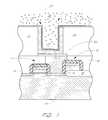
- FIG. 1is a schematic cross-section of one embodiment of a partially fabricated memory cell
- FIG. 2is a schematic cross-section of a conductor-insulator-conductor structure of FIG. 1;
- FIG. 3is the schematic cross-section of FIG. 2 illustrating the presence of oxygen vacancies and trapped oxygen atoms within the conductor-insulator-conductor structure
- FIG. 4is a schematic cross-section of the memory cell of FIG. 1 further incorporating the conductor-insulator-conductor structure of FIG. 2 with an overlying dielectric.
- DRAMdynamic random access memory
- embodiments of the inventioncan be used to improve a wide range of products and processes.
- the inventioncan be used to improve materials with high dielectric constants, metal-oxide-semiconductor structures, metal-oxide-metal structures and the like.
- FIG. 1illustrates a partially fabricated memory cell 4 formed within and over a semiconductor substrate 10 , in accordance with one embodiment of the present invention. While the illustrated substrate 10 comprises an intrinsically doped monocrystalline silicon wafer, it will be understood by one of skill in the art of semiconductor fabrication that the “substrate” in other arrangements can comprise other forms of semiconductor layers which include active or operable portions of semiconductor devices.
- a plurality of transistor gate electrodes 12overlie the substrate 10 , adjacent transistor active areas 14 within the substrate 10 . It will be understood that several transistors are formed across a memory array within a DRAM circuit or chip.
- Field oxide elements 16isolate the active areas 14 of different transistors. In the illustrated embodiment of FIG. 1, the field oxide elements 16 are formed using the well known local oxidation of silicon process (LOCOS). However, it is to be understood that the field oxide elements 16 could be formed using other processes such as shallow trench isolation (STI).
- the width of the gatesare preferably less than about 0.25 microns ( ⁇ m).
- the field oxide elements 16are formed using the well known LOCOS (Local Oxidation of Silicon) technique. However, in another embodiment, the field oxide elements 16 could be fabricated by another process, such as STI (Shallow Trench Issolation).
- LOCOSLocal Oxidation of Silicon
- STIShallow Trench Issolation
- a first insulating layer 18is shown covering the gate electrodes 12 .
- this insulating layer 18comprises a form of oxide, such as borophosphosilicate glass (BPSG).
- BPSGborophosphosilicate glass
- the first insulating layer 18typically has a thickness between about 0.15 ⁇ m to 1.5 ⁇ m.
- certain DRAM circuit designscall for “buried” digit lines running below the cell capacitors, such that a thicker insulating layer is required to electrically isolated the digit line from the underlying transistors and the overlying capacitors.
- a conductive contact 20is shown extending through the first insulating layer 18 to electrically contact an active area 14 between gate electrodes.
- the material of the contact 20comprises conductively doped polycrystalline silicon or polysilicon, which advantageously can be deposited into deep, narrow contact vias with good step coverage by chemical vapor deposition (CVD).
- CVDchemical vapor deposition
- the conductive contactshall be referred to as a “poly plug” 20 .
- the poly plug 20can include a variety of conductors including tungsten (W), aluminum (Al) or the like. As described in further detail below, the poly plug 20 has a reduced level of oxidation that occurs when removing oxygen vacancies from the memory cell 4 .
- the barrier layer 32advantageously acts as a diffusion barrier to reduce oxidation of the underlying poly plug 20 .
- the barrier layer 32may comprise tantalum (Ta), tantalum nitride (TaN), tantalum silicon nitride (TaSiN), titanium nitride (TiN), titanium aluminum nitride (TiAlN), titanium silicon nitride (TiSiN), tungsten nitride (WN x ), tungsten silicon nitride (WSiN), silicon nitride (SiN), molybdenum (Mo) or the like.
- Tatantalum nitride
- TaSiNtantalum silicon nitride
- TiNtitanium aluminum nitride
- TiAlNtitanium silicon nitride
- TiSiNtitanium silicon nitride
- WN xtungsten nitride
- WSiNsilicon nitride
- Momo
- the barrier layer 32can be formed by nitridizing a metallic film, such as Ta, Mo, Ti, and W, deposited on the poly plug 20 or by chemical vapor deposition (CVD), metal organic chemical vapor deposition (MOCVD), low temperature sputtering or the like.
- CVDchemical vapor deposition
- MOCVDmetal organic chemical vapor deposition
- the barrier layer 32is approximately 10 angstroms ( ⁇ ) to approximately 1000 or more angstroms ( ⁇ ) thick. In certain other embodiments, the barrier layer 32 is not used.
- a structural layer 22is then formed over the first insulating layer 18 and the barrier layer 32 .
- this structural layer 22need not become a permanent part of the circuit. Accordingly, the skilled artisan has a great deal of flexibility in the selection of this material.
- the structural layer 22is selectively etchable relative to the underlying first insulating layer 18 .
- the structural layer 22is BPSG.
- the surface area and thus the capacitance of the memory cell 4is influenced by the thickness of the structural layer 22 .
- the structural layer 22preferably has a thickness of greater than about 0.4 ⁇ m, more preferably between about 0.4 ⁇ m and 2.0 ⁇ m.
- a via 24is formed in the structural layer 22 to expose the underlying poly plug 20 , and a conductive layer 26 is deposited over the structural layer 22 and into the via 24 to coat the inner surfaces of the via 24 and to make electrical contact with the poly plug 20 .
- the top of the structural layer 22 , and the portion of the conductive layer 26 overlying the structural layer 22can then be planarized to leave the conductive layer 26 isolated within the via 24 , as shown in FIG. 1 .
- Such planarizationcan be accomplished by mechanical abrasion, preferably chemically aided by etchants in a slurry in a chemical mechanical planarization or polishing (CMP) process.
- CMPchemical mechanical planarization or polishing
- the conductive layer 26serves as a bottom electrode of the memory cell 4 , and can comprise a conductively doped polysilicon, hemispherical grain (HSG) polysilicon, platinum (Pt), ruthenium (Ru), ruthenium oxide (RuO x ), iridium (Ir), iridium oxide (IrO x ), palladium (Pd), tungsten (W) tungsten nitride (WN x ), tantalum nitride (TaN), titanium nitride (TiN), titanium oxygen nitride (TiON) or the like.
- HSGhemispherical grain
- the illustrated conductive layer 26thus takes on a three-dimensional folding shape that is of greater surface area than the area of the substrate 10 which the memory cell 4 occupies.
- Other methods of increasing surface areacan include creating a rough surface on the conductive layer 26 , creating multiple concentric container shapes for one memory cell, and creating a bottom electrode stud. The skilled artisan will find application for the processes and materials discussed below for any of a number of capacitor configurations.
- the conductive layer 26can be deposited by chemical vapor deposition (CVD), Low Pressure Chemical Vapor Deposition (LPCVD), metal organic chemical vapor deposition (MOCVD), plasma enhanced chemical vapor deposition (PECVD), physical vapor deposition (PVD), electroplating, or the like. While the thickness of the conductive layer 26 is approximately 100 angstroms ( ⁇ ) to approximately 1000 ( ⁇ ), the skilled artisan will recognize that the thickness of the conductive layer 26 can vary over a wide variety of ranges.
- CVDchemical vapor deposition
- LPCVDLow Pressure Chemical Vapor Deposition
- MOCVDmetal organic chemical vapor deposition
- PECVDplasma enhanced chemical vapor deposition
- PVDphysical vapor deposition
- electroplatingelectroplating, or the like. While the thickness of the conductive layer 26 is approximately 100 angstroms ( ⁇ ) to approximately 1000 ( ⁇ ), the skilled artisan will recognize that the thickness of the conductive layer 26 can vary over a wide variety of ranges.
- the memory cell 4further comprises an insulating layer 34 which is deposited above the conductive layer 26 and above the structural layer 22 .
- the insulating layer 34forms a part of a conductor -insulator- conductor (CIC) structure 30 of the memory cell 4 .
- the insulating layer 34is an insulator that provides electrical insulation.
- the insulating layer 34is a conventional dielectric material such as silicon nitride.
- the insulating layer 34is a material with a high dielectric constant. Materials having high dielectric constants greater than 9 are to be distinguished from conventional dielectric materials such as silicon nitride which has a dielectric constant of approximately 7.
- the high constant dielectric materialstypically comprise inorganic non-metallic oxides such as aluminum oxide (Al 2 O 3 ), tantalum pentoxide (Ta 2 O 5 ), oxide paraelectric materials, and ferroelectric materials, including by way of example, barium strontium titanate ((BaSr)TiO 3 or BST), strontium titanate (ST), barium titanate (BT), lead zirconium titanate (PZT), strontium bismuth tantalate (SBT), or the like.
- inorganic non-metallic oxidessuch as aluminum oxide (Al 2 O 3 ), tantalum pentoxide (Ta 2 O 5 ), oxide paraelectric materials, and ferroelectric materials, including by way of example, barium strontium titanate ((BaSr)TiO 3 or BST), strontium titanate (ST), barium titanate (BT), lead zirconium titanate (PZT), strontium bismuth tantalate (SBT), or the like.
- the insulating layer 34comprises material in a crystalline state.
- the insulating layer 34could comprise material in a non-crystalline state.
- the insulating layer 34could comprise an amorphous dielectric material.
- the dielectric 34is deposited by alternating current (AC) sputtering at a temperature range of approximately 50° C. to approximately 700° C.
- a target materialcan comprise a stoichiometric composition of powdered materials.
- the thickness of such a dielectric layeris preferably in the range of approximately 20 ⁇ to approximately 500 ⁇ thick.
- Other deposition techniquessuch as CVD, LPCVD, PECVD or MOCVD can be utilized.
- the dielectric 34comprises tantalum pentoxide and is between approximately 40 ⁇ and approximately 120 ⁇ thick.
- the tantalum pentoxideis approximately 70 ⁇ thick.
- the dielectric constant (k) of tantalum pentoxideis 25 to 50, and when doped with silicon can increase up to 130.
- tantalum pentoxidecan be formed by chemical vapor deposition, using an organometallic precursor.
- the dielectric 34comprises barium strontium titanate that is between approximately 100 ⁇ and approximately 500 ⁇ thick.
- the barium strontium titanateis approximately 200 ⁇ to approximately 300 ⁇ thick.
- the dielectric constant (k) of the barium strontium titanatevaries from about 100 to 600, depending upon the phase and thickness of the material, the preferred dielectric 34 has a dielectric constant of about 300.
- barium strontium titanateis preferably deposited by chemical vapor deposition techniques comprising reacting volatile complexes containing barium (Ba), strontium (Sr and titanium (Ti) in an oxygen ambient.
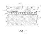
- FIG. 2illustrates the conductor-insulator-conductor (CIC) structure 30 of the memory cell 4 of FIG. 1 .
- the CIC 30comprises the conductive layer 26 , the dielectric 34 , and the second conductive layer 36 .
- the conductive layer 26is hereinafter referred to as the bottom electrode 26 and the conductive layer 36 is hereinafter referred to as the upper electrode 36 .
- the dielectric 34comprising tantalum pentoxide or barium strontium titanate may contain defects where missing oxygen atoms deform their crystalline structures and yield poor dielectric properties such as lower dielectric constants and higher leakage currents.
- one embodiment of the inventionreduces the oxygen vacancies in the dielectric 34 by exposing the CIC 30 to a strongly oxidizing ambient having an increased concentration of oxygen atoms 37 while the second conductive layer 36 is deposited above the dielectric 34 .
- the upper electrode 36is deposited over the dielectric 34 .
- the upper electrode 36typically comprises platinum (Pt), ruthenium (Ru), ruthenium oxide (RuO x ), iridium (Ir), iridium oxide (IrO x ), palladium (Pd), tungsten (W), tungsten nitride (WN), tantalum nitride (TaN), titanium nitride (TiN), titanium oxygen nitride (TiON), or the like.
- a suitable deposition processis sputtering, CVD, LPCVD, PECVD, MOCVD or the like.
- the upper electrode 36is preferably deposited to a thickness range of approximately 100 ⁇ to approximately 2000 ⁇ .
- an electrodeis typically deposited in an ambient having only enough oxygen to provide the electrode with a stable stoichiometry.
- the oxygen concentrationis typically chosen so that stoichemetrically stable IrO 2 is formed.
- the upper electrode 36 of the preferred embodiment of the present inventionis deposited over the dielectric 34 in the strongly oxidizing ambient 35 .
- the upper electrode 36is highly oxidized such that the quantity of oxygen atoms within the upper electrode is greater than that which is required for stoicheometric stability.
- the upper electrode 36is formed of IrO x wherein x is greater than 2.0 and less than 2.5 such that the electrical properties of the upper electrode 36 are not substantially affected by the excess oxygen atoms.
- depositing the upper electrode 36 in the strongly oxidizing ambient 35provides many advantages as will now be described in connection with FIG. 3 .
- the dielectric 34is initially exposed to the ambient 35 and since the ambient 35 comprises the relatively high concentration of oxygen atoms 37 , a relatively large number of oxygen atoms immediately diffuse into the dielectric 34 .
- a relatively large number of oxygen atoms from the ambient 35combine with the oxygen vacancies 40 in the dielectric 34 so as to provide a reduced concentration of oxygen vacancies 40 in the dielectric 34 .
- the reduced concentration of oxygen vacancies 40 in the dielectric 34provide the CIC 30 with increased capacitance and decreased leakage currents.
- Another advantage provided by depositing the upper electrode 36 in the strongly oxidizing ambient 35is the formation of an oxygen-rich interface layer 42 between the dielectric 34 and the upper electrode 36 .
- a relatively large number of oxygen atoms 37 from the strongly oxidizing ambient 35engage with the exposed surface of the dielectric 34 and are subsequently trapped by the overlying upper electrode 36 so as to form the layer 42 which acts as an oxygen vacancy sink. Consequently, in the event that some of the oxygen vacancies 40 of the dielectric layer 34 migrate toward the interface layer 42 , the migrating oxygen vacancies 40 will likely combine with the oxygen of the interface layer 42 .
- Yet another advantage provided by depositing the upper electrode 36 in the strongly oxidizing ambient 35is the trapping of oxygen atoms at a plurality of oxygen-rich regions 44 throughout the upper electrode 36 .
- the trapped oxygen atoms of the regions 44 in the upper electrode 36provide an increased capacity for absorbing oxygen vacancies that migrate into the upper electrode 36 .
- the trapped oxygen atoms of the regions 44 of the upper electrode 36assist in further providing the CIC 30 with an increased capacitance and an increased resistance to leakage currents.
- Still yet another advantage provided by depositing the upper electrode 36 in the strongly oxidizing ambient 35is that of reduced manufacturing time.
- depositing the upper electrode 36 in the strongly oxidizing ambient 35provides the CIC 30 with the reduced concentration of oxygen vacancies 40 , the need for conventional annealing processes designed to reduce the oxygen vacancies 40 is reduced.
- the memory cell 4can be manufactured in less time.
- a third conductive layer 38may exist above the upper electrode 36 .
- the third conductive layer 38forms a part of the top electrode 36 .
- Exemplary materials for the third conductive layer 38include polysilicon, tungsten, tungsten nitride (WN x ), and titanium nitride (TiN).
- ILD 41has also been formed over the upper electrode 36 .
- the ILD 41comprises a form of oxide, such as borophosphosilicate glass (BPSG).
- BPSGborophosphosilicate glass
- Deposition of the BPSGmay be followed by a reflow anneal step for better step coverage and avoiding keyholes, as well as to densify the layer.
- the reflowis conducted by heating the wafer to temperatures of approximately 550° C. to 900° C. If not separately annealed before this point, the deposited amorphous dielectric 34 can be converted to a crystalline phase during this high temperature reflow.
- contactsare created through the BPSG 41 to connect the top electrode 36 , 38 to wiring formed above or within the BPSG 41 .
- the CIC 30could be exposed to an additional processing step whereby the oxygen vacancies 38 are induced to migrate toward the interface layer 42 (FIG. 3 ).
- the memory cell 4is exposed to an electric field in a well known manner that urges a portion of the remaining oxygen vacancies 40 in the dielectric layer 34 to migrate toward the interface layer 42 .
- the oxygen-rich interface layer 42subsequently absorbs the displaced oxygen vacancies, thereby preventing the buildup of oxygen vacancies at the interface layer 42 and further reducing the concentration of oxygen vacancies 38 within the dielectric 34 .
- the preferred embodiments of the CIC 30 of the present inventionprovide improved capacitance and reduced leakage currents. Such improvements are realized by exposing the dielectric 34 of the CIC 30 to the strongly oxidizing ambient 35 during the deposition process of the upper electrode 36 . This reduces the concentration of oxygen vacancies 40 of the dielectric 34 to thereby increase the dielectric constant and the resistance of the dielectric 34 .
Landscapes
- Engineering & Computer Science (AREA)
- Physics & Mathematics (AREA)
- Condensed Matter Physics & Semiconductors (AREA)
- General Physics & Mathematics (AREA)
- Computer Hardware Design (AREA)
- Microelectronics & Electronic Packaging (AREA)
- Power Engineering (AREA)
- Manufacturing & Machinery (AREA)
- Chemical & Material Sciences (AREA)
- Materials Engineering (AREA)
- Semiconductor Memories (AREA)
Abstract
Description
Claims (35)
Priority Applications (3)
| Application Number | Priority Date | Filing Date | Title |
|---|---|---|---|
| US09/652,863US6682969B1 (en) | 2000-08-31 | 2000-08-31 | Top electrode in a strongly oxidizing environment |
| US10/039,215US7023043B2 (en) | 2000-08-31 | 2002-01-03 | Top electrode in a strongly oxidizing environment |
| US11/398,498US20070069270A1 (en) | 2000-08-31 | 2006-04-04 | Top electrode in a strongly oxidizing environment |
Applications Claiming Priority (1)
| Application Number | Priority Date | Filing Date | Title |
|---|---|---|---|
| US09/652,863US6682969B1 (en) | 2000-08-31 | 2000-08-31 | Top electrode in a strongly oxidizing environment |
Related Child Applications (1)
| Application Number | Title | Priority Date | Filing Date |
|---|---|---|---|
| US10/039,215DivisionUS7023043B2 (en) | 2000-08-31 | 2002-01-03 | Top electrode in a strongly oxidizing environment |
Publications (1)
| Publication Number | Publication Date |
|---|---|
| US6682969B1true US6682969B1 (en) | 2004-01-27 |
Family
ID=24618493
Family Applications (3)
| Application Number | Title | Priority Date | Filing Date |
|---|---|---|---|
| US09/652,863Expired - Fee RelatedUS6682969B1 (en) | 2000-08-31 | 2000-08-31 | Top electrode in a strongly oxidizing environment |
| US10/039,215Expired - Fee RelatedUS7023043B2 (en) | 2000-08-31 | 2002-01-03 | Top electrode in a strongly oxidizing environment |
| US11/398,498AbandonedUS20070069270A1 (en) | 2000-08-31 | 2006-04-04 | Top electrode in a strongly oxidizing environment |
Family Applications After (2)
| Application Number | Title | Priority Date | Filing Date |
|---|---|---|---|
| US10/039,215Expired - Fee RelatedUS7023043B2 (en) | 2000-08-31 | 2002-01-03 | Top electrode in a strongly oxidizing environment |
| US11/398,498AbandonedUS20070069270A1 (en) | 2000-08-31 | 2006-04-04 | Top electrode in a strongly oxidizing environment |
Country Status (1)
| Country | Link |
|---|---|
| US (3) | US6682969B1 (en) |
Cited By (37)
| Publication number | Priority date | Publication date | Assignee | Title |
|---|---|---|---|---|
| US20030183936A1 (en)* | 2002-03-28 | 2003-10-02 | Matsushita Electric Industrial Co., Ltd. | Semiconductor device and method for fabricating the same |
| US20030207593A1 (en)* | 2002-05-02 | 2003-11-06 | Micron Technology, Inc. | Atomic layer deposition and conversion |
| US20040063275A1 (en)* | 2001-06-12 | 2004-04-01 | Hynix Semiconductor Inc. | Capacitor of a semiconductor memory device and method of forming the seme |
| US20040087100A1 (en)* | 2001-06-15 | 2004-05-06 | Gousev Evgeni P. | High-dielectric constant insulators for feol capacitors |
| US20040208833A1 (en)* | 2003-02-04 | 2004-10-21 | Elan Pharma International Ltd. | Novel fluticasone formulations |
| US20060033140A1 (en)* | 2004-08-13 | 2006-02-16 | Graettinger Thomas M | Memory circuitry |
| US20070048953A1 (en)* | 2005-08-30 | 2007-03-01 | Micron Technology, Inc. | Graded dielectric layers |
| US20070051999A1 (en)* | 2005-09-05 | 2007-03-08 | Samsung Electronics Co., Ltd. | Ferroelectric capacitor having three-dimensional structure, nonvolatile memory device having the same and method of fabricating the same |
| US20070101929A1 (en)* | 2002-05-02 | 2007-05-10 | Micron Technology, Inc. | Methods for atomic-layer deposition |
| US20080254204A1 (en)* | 2007-04-16 | 2008-10-16 | Infineon Technologies Ag | Dielectric apparatus and associated methods |
| US20100081293A1 (en)* | 2008-10-01 | 2010-04-01 | Applied Materials, Inc. | Methods for forming silicon nitride based film or silicon carbon based film |
| US20110034039A1 (en)* | 2009-08-06 | 2011-02-10 | Applied Materials, Inc. | Formation of silicon oxide using non-carbon flowable cvd processes |
| US20110111137A1 (en)* | 2009-11-12 | 2011-05-12 | Applied Materials, Inc. | Curing non-carbon flowable cvd films |
| US20110129616A1 (en)* | 2009-12-02 | 2011-06-02 | Applied Materials, Inc. | Oxygen-doping for non-carbon radical-component cvd films |
| US20110159213A1 (en)* | 2009-12-30 | 2011-06-30 | Applied Materials, Inc. | Chemical vapor deposition improvements through radical-component modification |
| US20110159703A1 (en)* | 2009-12-30 | 2011-06-30 | Applied Materials, Inc. | Dielectric film growth with radicals produced using flexible nitrogen/hydrogen ratio |
| US20110165781A1 (en)* | 2010-01-06 | 2011-07-07 | Applied Materials, Inc. | Flowable dielectric using oxide liner |
| WO2012015610A3 (en)* | 2010-07-30 | 2012-04-26 | Applied Materials, Inc. | Oxide-rich liner layer for flowable cvd gapfill |
| US8304351B2 (en) | 2010-01-07 | 2012-11-06 | Applied Materials, Inc. | In-situ ozone cure for radical-component CVD |
| US8329262B2 (en) | 2010-01-05 | 2012-12-11 | Applied Materials, Inc. | Dielectric film formation using inert gas excitation |
| US8445078B2 (en) | 2011-04-20 | 2013-05-21 | Applied Materials, Inc. | Low temperature silicon oxide conversion |
| US8450191B2 (en) | 2011-01-24 | 2013-05-28 | Applied Materials, Inc. | Polysilicon films by HDP-CVD |
| US8466073B2 (en) | 2011-06-03 | 2013-06-18 | Applied Materials, Inc. | Capping layer for reduced outgassing |
| US8501563B2 (en) | 2005-07-20 | 2013-08-06 | Micron Technology, Inc. | Devices with nanocrystals and methods of formation |
| US8551891B2 (en) | 2011-10-04 | 2013-10-08 | Applied Materials, Inc. | Remote plasma burn-in |
| US8563445B2 (en) | 2010-03-05 | 2013-10-22 | Applied Materials, Inc. | Conformal layers by radical-component CVD |
| US8617989B2 (en) | 2011-09-26 | 2013-12-31 | Applied Materials, Inc. | Liner property improvement |
| US8664127B2 (en) | 2010-10-15 | 2014-03-04 | Applied Materials, Inc. | Two silicon-containing precursors for gapfill enhancing dielectric liner |
| US20140092666A1 (en)* | 2012-09-28 | 2014-04-03 | Elijah V. Karpov | Low voltage embedded memory having conductive oxide and electrode stacks |
| US8716154B2 (en) | 2011-03-04 | 2014-05-06 | Applied Materials, Inc. | Reduced pattern loading using silicon oxide multi-layers |
| US8889566B2 (en) | 2012-09-11 | 2014-11-18 | Applied Materials, Inc. | Low cost flowable dielectric films |
| US9018108B2 (en) | 2013-01-25 | 2015-04-28 | Applied Materials, Inc. | Low shrinkage dielectric films |
| US9285168B2 (en) | 2010-10-05 | 2016-03-15 | Applied Materials, Inc. | Module for ozone cure and post-cure moisture treatment |
| US9404178B2 (en) | 2011-07-15 | 2016-08-02 | Applied Materials, Inc. | Surface treatment and deposition for reduced outgassing |
| US9412581B2 (en) | 2014-07-16 | 2016-08-09 | Applied Materials, Inc. | Low-K dielectric gapfill by flowable deposition |
| US9520460B2 (en) | 2013-09-05 | 2016-12-13 | Samsung Electronics Co., Ltd. | MIM capacitors with diffusion-blocking electrode structures and semiconductor devices including the same |
| US10283321B2 (en) | 2011-01-18 | 2019-05-07 | Applied Materials, Inc. | Semiconductor processing system and methods using capacitively coupled plasma |
Families Citing this family (25)
| Publication number | Priority date | Publication date | Assignee | Title |
|---|---|---|---|---|
| US6943392B2 (en)* | 1999-08-30 | 2005-09-13 | Micron Technology, Inc. | Capacitors having a capacitor dielectric layer comprising a metal oxide having multiple different metals bonded with oxygen |
| US6558517B2 (en)* | 2000-05-26 | 2003-05-06 | Micron Technology, Inc. | Physical vapor deposition methods |
| US20030017266A1 (en)* | 2001-07-13 | 2003-01-23 | Cem Basceri | Chemical vapor deposition methods of forming barium strontium titanate comprising dielectric layers, including such layers having a varied concentration of barium and strontium within the layer |
| US6838122B2 (en)* | 2001-07-13 | 2005-01-04 | Micron Technology, Inc. | Chemical vapor deposition methods of forming barium strontium titanate comprising dielectric layers |
| US7011978B2 (en)* | 2001-08-17 | 2006-03-14 | Micron Technology, Inc. | Methods of forming capacitor constructions comprising perovskite-type dielectric materials with different amount of crystallinity regions |
| US6967154B2 (en) | 2002-08-26 | 2005-11-22 | Micron Technology, Inc. | Enhanced atomic layer deposition |
| US6803275B1 (en) | 2002-12-03 | 2004-10-12 | Fasl, Llc | ONO fabrication process for reducing oxygen vacancy content in bottom oxide layer in flash memory devices |
| US7033957B1 (en) | 2003-02-05 | 2006-04-25 | Fasl, Llc | ONO fabrication process for increasing oxygen content at bottom oxide-substrate interface in flash memory devices |
| US6720232B1 (en)* | 2003-04-10 | 2004-04-13 | Taiwan Semiconductor Manufacturing Company | Method of fabricating an embedded DRAM for metal-insulator-metal (MIM) capacitor structure |
| KR100510527B1 (en)* | 2003-05-01 | 2005-08-26 | 삼성전자주식회사 | Semiconductor device having storage node and method for manufacturing the same |
| US7312120B2 (en) | 2004-09-01 | 2007-12-25 | Micron Technology, Inc. | Method for obtaining extreme selectivity of metal nitrides and metal oxides |
| JP2008147594A (en)* | 2006-12-13 | 2008-06-26 | Matsushita Electric Ind Co Ltd | Semiconductor device and manufacturing method thereof |
| KR100972864B1 (en)* | 2008-05-21 | 2010-07-28 | 주식회사 하이닉스반도체 | Semiconductor memory device and capacitor formation method of semiconductor memory device |
| US8416609B2 (en) | 2010-02-15 | 2013-04-09 | Micron Technology, Inc. | Cross-point memory cells, non-volatile memory arrays, methods of reading a memory cell, methods of programming a memory cell, methods of writing to and reading from a memory cell, and computer systems |
| US8437174B2 (en)* | 2010-02-15 | 2013-05-07 | Micron Technology, Inc. | Memcapacitor devices, field effect transistor devices, non-volatile memory arrays, and methods of programming |
| US8634224B2 (en) | 2010-08-12 | 2014-01-21 | Micron Technology, Inc. | Memory cells, non-volatile memory arrays, methods of operating memory cells, methods of writing to and reading from a memory cell, and methods of programming a memory cell |
| CN102646790B (en)* | 2011-02-18 | 2014-06-04 | 华邦电子股份有限公司 | Non-volatile memory |
| CN102683583B (en)* | 2011-03-15 | 2014-04-09 | 北京大学 | Unipolar resistive random access memory and manufacturing method thereof |
| US8691681B2 (en)* | 2012-01-04 | 2014-04-08 | United Microelectronics Corp. | Semiconductor device having a metal gate and fabricating method thereof |
| CN102945923A (en)* | 2012-10-26 | 2013-02-27 | 清华大学 | Complementary type resistive random access memory and production method thereof |
| US20200203358A1 (en)* | 2017-09-27 | 2020-06-25 | Intel Corporation | Ferroelectrics using thin alloy of para-electric materials |
| US11121139B2 (en)* | 2017-11-16 | 2021-09-14 | International Business Machines Corporation | Hafnium oxide and zirconium oxide based ferroelectric devices with textured iridium bottom electrodes |
| US11251261B2 (en)* | 2019-05-17 | 2022-02-15 | Micron Technology, Inc. | Forming a barrier material on an electrode |
| CN115483289A (en)* | 2022-09-15 | 2022-12-16 | 中国科学院微电子研究所 | Ferroelectric field effect transistor, manufacturing method thereof and memory |
| US20250166898A1 (en)* | 2023-11-21 | 2025-05-22 | Nanya Technology Corporation | Capacitor and method of manufacturing thereof |
Citations (10)
| Publication number | Priority date | Publication date | Assignee | Title |
|---|---|---|---|---|
| US5191510A (en) | 1992-04-29 | 1993-03-02 | Ramtron International Corporation | Use of palladium as an adhesion layer and as an electrode in ferroelectric memory devices |
| EP0557937A1 (en) | 1992-02-25 | 1993-09-01 | Ramtron International Corporation | Ozone gas processing for ferroelectric memory circuits |
| US5814852A (en)* | 1995-05-19 | 1998-09-29 | Micron Technology, Inc. | Method of forming a Ta2 O5 dielectric layer, method of forming a capacitor having a Ta2 O5 dielectric layer, and capacitor construction |
| US6153490A (en)* | 1997-07-01 | 2000-11-28 | Texas Instruments Incorporated | Method for forming integrated circuit capacitor and memory |
| US6211035B1 (en) | 1998-09-09 | 2001-04-03 | Texas Instruments Incorporated | Integrated circuit and method |
| US6297085B1 (en) | 1997-12-11 | 2001-10-02 | Texas Instruments Incorporated | Method for manufacturing ferroelectric capacitor and method for manufacturing ferroelectric memory |
| US6309894B1 (en) | 1996-07-09 | 2001-10-30 | Hitachi, Ltd | Semiconductor memory and method of manufacturing the same |
| US6475854B2 (en)* | 1999-12-30 | 2002-11-05 | Applied Materials, Inc. | Method of forming metal electrodes |
| US6495412B1 (en)* | 1998-09-11 | 2002-12-17 | Fujitsu Limited | Semiconductor device having a ferroelectric capacitor and a fabrication process thereof |
| US6541813B1 (en)* | 1999-08-31 | 2003-04-01 | Kabushiki Kaisha Toshiba | Capacitor and method for manufacturing the same |
Family Cites Families (1)
| Publication number | Priority date | Publication date | Assignee | Title |
|---|---|---|---|---|
| US6103567A (en)* | 1999-08-10 | 2000-08-15 | Vanguard International Semiconductor Corp. | Method of fabricating dielectric layer |
- 2000
- 2000-08-31USUS09/652,863patent/US6682969B1/ennot_activeExpired - Fee Related
- 2002
- 2002-01-03USUS10/039,215patent/US7023043B2/ennot_activeExpired - Fee Related
- 2006
- 2006-04-04USUS11/398,498patent/US20070069270A1/ennot_activeAbandoned
Patent Citations (11)
| Publication number | Priority date | Publication date | Assignee | Title |
|---|---|---|---|---|
| EP0557937A1 (en) | 1992-02-25 | 1993-09-01 | Ramtron International Corporation | Ozone gas processing for ferroelectric memory circuits |
| US5191510A (en) | 1992-04-29 | 1993-03-02 | Ramtron International Corporation | Use of palladium as an adhesion layer and as an electrode in ferroelectric memory devices |
| US5814852A (en)* | 1995-05-19 | 1998-09-29 | Micron Technology, Inc. | Method of forming a Ta2 O5 dielectric layer, method of forming a capacitor having a Ta2 O5 dielectric layer, and capacitor construction |
| US6309894B1 (en) | 1996-07-09 | 2001-10-30 | Hitachi, Ltd | Semiconductor memory and method of manufacturing the same |
| US6420192B2 (en)* | 1996-07-09 | 2002-07-16 | Hitachi, Ltd. | Method of manufacturing semiconductor memory |
| US6153490A (en)* | 1997-07-01 | 2000-11-28 | Texas Instruments Incorporated | Method for forming integrated circuit capacitor and memory |
| US6297085B1 (en) | 1997-12-11 | 2001-10-02 | Texas Instruments Incorporated | Method for manufacturing ferroelectric capacitor and method for manufacturing ferroelectric memory |
| US6211035B1 (en) | 1998-09-09 | 2001-04-03 | Texas Instruments Incorporated | Integrated circuit and method |
| US6495412B1 (en)* | 1998-09-11 | 2002-12-17 | Fujitsu Limited | Semiconductor device having a ferroelectric capacitor and a fabrication process thereof |
| US6541813B1 (en)* | 1999-08-31 | 2003-04-01 | Kabushiki Kaisha Toshiba | Capacitor and method for manufacturing the same |
| US6475854B2 (en)* | 1999-12-30 | 2002-11-05 | Applied Materials, Inc. | Method of forming metal electrodes |
Cited By (61)
| Publication number | Priority date | Publication date | Assignee | Title |
|---|---|---|---|---|
| US20040063275A1 (en)* | 2001-06-12 | 2004-04-01 | Hynix Semiconductor Inc. | Capacitor of a semiconductor memory device and method of forming the seme |
| US6958506B2 (en)* | 2001-06-15 | 2005-10-25 | International Business Machines Corporation | High-dielectric constant insulators for feol capacitors |
| US20040087100A1 (en)* | 2001-06-15 | 2004-05-06 | Gousev Evgeni P. | High-dielectric constant insulators for feol capacitors |
| US7268036B2 (en) | 2002-03-28 | 2007-09-11 | Matsushita Electric Industrial Co., Ltd. | Semiconductor device and method for fabricating the same |
| US20030183936A1 (en)* | 2002-03-28 | 2003-10-02 | Matsushita Electric Industrial Co., Ltd. | Semiconductor device and method for fabricating the same |
| US6831323B2 (en)* | 2002-03-28 | 2004-12-14 | Matsushita Electric Industrial Co., Ltd. | Semiconductor device and method for fabricating the same |
| US20050023584A1 (en)* | 2002-05-02 | 2005-02-03 | Micron Technology, Inc. | Atomic layer deposition and conversion |
| US20070101929A1 (en)* | 2002-05-02 | 2007-05-10 | Micron Technology, Inc. | Methods for atomic-layer deposition |
| US7670646B2 (en) | 2002-05-02 | 2010-03-02 | Micron Technology, Inc. | Methods for atomic-layer deposition |
| US7589029B2 (en) | 2002-05-02 | 2009-09-15 | Micron Technology, Inc. | Atomic layer deposition and conversion |
| US7560793B2 (en) | 2002-05-02 | 2009-07-14 | Micron Technology, Inc. | Atomic layer deposition and conversion |
| US20030207593A1 (en)* | 2002-05-02 | 2003-11-06 | Micron Technology, Inc. | Atomic layer deposition and conversion |
| US20040208833A1 (en)* | 2003-02-04 | 2004-10-21 | Elan Pharma International Ltd. | Novel fluticasone formulations |
| US7126182B2 (en) | 2004-08-13 | 2006-10-24 | Micron Technology, Inc. | Memory circuitry |
| US20060249772A1 (en)* | 2004-08-13 | 2006-11-09 | Graettinger Thomas M | Memory circuitry |
| US20060033140A1 (en)* | 2004-08-13 | 2006-02-16 | Graettinger Thomas M | Memory circuitry |
| US7495277B2 (en) | 2004-08-13 | 2009-02-24 | Micron Technology, Inc. | Memory circuitry |
| US8921914B2 (en) | 2005-07-20 | 2014-12-30 | Micron Technology, Inc. | Devices with nanocrystals and methods of formation |
| US8501563B2 (en) | 2005-07-20 | 2013-08-06 | Micron Technology, Inc. | Devices with nanocrystals and methods of formation |
| US8951903B2 (en) | 2005-08-30 | 2015-02-10 | Micron Technology, Inc. | Graded dielectric structures |
| US20070048953A1 (en)* | 2005-08-30 | 2007-03-01 | Micron Technology, Inc. | Graded dielectric layers |
| US9627501B2 (en) | 2005-08-30 | 2017-04-18 | Micron Technology, Inc. | Graded dielectric structures |
| US8110469B2 (en) | 2005-08-30 | 2012-02-07 | Micron Technology, Inc. | Graded dielectric layers |
| US7910967B2 (en)* | 2005-09-05 | 2011-03-22 | Samsung Electronics Co., Ltd. | Ferroelectric capacitor having three-dimensional structure, nonvolatile memory device having the same and method of fabricating the same |
| US20070051999A1 (en)* | 2005-09-05 | 2007-03-08 | Samsung Electronics Co., Ltd. | Ferroelectric capacitor having three-dimensional structure, nonvolatile memory device having the same and method of fabricating the same |
| US20080254204A1 (en)* | 2007-04-16 | 2008-10-16 | Infineon Technologies Ag | Dielectric apparatus and associated methods |
| US20100081293A1 (en)* | 2008-10-01 | 2010-04-01 | Applied Materials, Inc. | Methods for forming silicon nitride based film or silicon carbon based film |
| US20110034039A1 (en)* | 2009-08-06 | 2011-02-10 | Applied Materials, Inc. | Formation of silicon oxide using non-carbon flowable cvd processes |
| US8741788B2 (en) | 2009-08-06 | 2014-06-03 | Applied Materials, Inc. | Formation of silicon oxide using non-carbon flowable CVD processes |
| US8449942B2 (en) | 2009-11-12 | 2013-05-28 | Applied Materials, Inc. | Methods of curing non-carbon flowable CVD films |
| US20110111137A1 (en)* | 2009-11-12 | 2011-05-12 | Applied Materials, Inc. | Curing non-carbon flowable cvd films |
| US8980382B2 (en) | 2009-12-02 | 2015-03-17 | Applied Materials, Inc. | Oxygen-doping for non-carbon radical-component CVD films |
| US20110129616A1 (en)* | 2009-12-02 | 2011-06-02 | Applied Materials, Inc. | Oxygen-doping for non-carbon radical-component cvd films |
| US20110159703A1 (en)* | 2009-12-30 | 2011-06-30 | Applied Materials, Inc. | Dielectric film growth with radicals produced using flexible nitrogen/hydrogen ratio |
| US20110159213A1 (en)* | 2009-12-30 | 2011-06-30 | Applied Materials, Inc. | Chemical vapor deposition improvements through radical-component modification |
| US8629067B2 (en) | 2009-12-30 | 2014-01-14 | Applied Materials, Inc. | Dielectric film growth with radicals produced using flexible nitrogen/hydrogen ratio |
| US8329262B2 (en) | 2010-01-05 | 2012-12-11 | Applied Materials, Inc. | Dielectric film formation using inert gas excitation |
| US20110165781A1 (en)* | 2010-01-06 | 2011-07-07 | Applied Materials, Inc. | Flowable dielectric using oxide liner |
| US8647992B2 (en) | 2010-01-06 | 2014-02-11 | Applied Materials, Inc. | Flowable dielectric using oxide liner |
| US8304351B2 (en) | 2010-01-07 | 2012-11-06 | Applied Materials, Inc. | In-situ ozone cure for radical-component CVD |
| US8563445B2 (en) | 2010-03-05 | 2013-10-22 | Applied Materials, Inc. | Conformal layers by radical-component CVD |
| WO2012015610A3 (en)* | 2010-07-30 | 2012-04-26 | Applied Materials, Inc. | Oxide-rich liner layer for flowable cvd gapfill |
| CN103038868A (en)* | 2010-07-30 | 2013-04-10 | 应用材料公司 | Oxide-rich liner layer for flowable cvd gapfill |
| US9285168B2 (en) | 2010-10-05 | 2016-03-15 | Applied Materials, Inc. | Module for ozone cure and post-cure moisture treatment |
| US8664127B2 (en) | 2010-10-15 | 2014-03-04 | Applied Materials, Inc. | Two silicon-containing precursors for gapfill enhancing dielectric liner |
| US10283321B2 (en) | 2011-01-18 | 2019-05-07 | Applied Materials, Inc. | Semiconductor processing system and methods using capacitively coupled plasma |
| US8450191B2 (en) | 2011-01-24 | 2013-05-28 | Applied Materials, Inc. | Polysilicon films by HDP-CVD |
| US8716154B2 (en) | 2011-03-04 | 2014-05-06 | Applied Materials, Inc. | Reduced pattern loading using silicon oxide multi-layers |
| US8445078B2 (en) | 2011-04-20 | 2013-05-21 | Applied Materials, Inc. | Low temperature silicon oxide conversion |
| US8466073B2 (en) | 2011-06-03 | 2013-06-18 | Applied Materials, Inc. | Capping layer for reduced outgassing |
| US9404178B2 (en) | 2011-07-15 | 2016-08-02 | Applied Materials, Inc. | Surface treatment and deposition for reduced outgassing |
| US8617989B2 (en) | 2011-09-26 | 2013-12-31 | Applied Materials, Inc. | Liner property improvement |
| US8551891B2 (en) | 2011-10-04 | 2013-10-08 | Applied Materials, Inc. | Remote plasma burn-in |
| US8889566B2 (en) | 2012-09-11 | 2014-11-18 | Applied Materials, Inc. | Low cost flowable dielectric films |
| US20140092666A1 (en)* | 2012-09-28 | 2014-04-03 | Elijah V. Karpov | Low voltage embedded memory having conductive oxide and electrode stacks |
| US9231204B2 (en)* | 2012-09-28 | 2016-01-05 | Intel Corporation | Low voltage embedded memory having conductive oxide and electrode stacks |
| US20160079523A1 (en)* | 2012-09-28 | 2016-03-17 | Elijah V. Karpov | Low voltage embedded memory having conductive oxide and electrode stacks |
| US9647208B2 (en)* | 2012-09-28 | 2017-05-09 | Intel Corporation | Low voltage embedded memory having conductive oxide and electrode stacks |
| US9018108B2 (en) | 2013-01-25 | 2015-04-28 | Applied Materials, Inc. | Low shrinkage dielectric films |
| US9520460B2 (en) | 2013-09-05 | 2016-12-13 | Samsung Electronics Co., Ltd. | MIM capacitors with diffusion-blocking electrode structures and semiconductor devices including the same |
| US9412581B2 (en) | 2014-07-16 | 2016-08-09 | Applied Materials, Inc. | Low-K dielectric gapfill by flowable deposition |
Also Published As
| Publication number | Publication date |
|---|---|
| US20020084480A1 (en) | 2002-07-04 |
| US20070069270A1 (en) | 2007-03-29 |
| US7023043B2 (en) | 2006-04-04 |
Similar Documents
| Publication | Publication Date | Title |
|---|---|---|
| US6682969B1 (en) | Top electrode in a strongly oxidizing environment | |
| US6686620B2 (en) | FRAM and method of fabricating the same | |
| US6737694B2 (en) | Ferroelectric memory device and method of forming the same | |
| US6281142B1 (en) | Dielectric cure for reducing oxygen vacancies | |
| US6320244B1 (en) | Integrated circuit device having dual damascene capacitor | |
| US6518070B1 (en) | Process of forming a semiconductor device and a semiconductor device | |
| US6940112B2 (en) | Integrated capacitors fabricated with conductive metal oxides | |
| US6965140B2 (en) | Semiconductor device including storage capacitor | |
| US6750500B1 (en) | Capacitor electrode for integrating high K materials | |
| US6730955B2 (en) | Semiconductor memory and process for fabricating the same | |
| US6888189B2 (en) | Dielectric element including oxide-based dielectric film and method of fabricating the same | |
| CN100362626C (en) | Capacitor barrier in plug structure | |
| US20030173613A1 (en) | Memory-storage node and the method of fabricating the same | |
| US20040089891A1 (en) | Semiconductor device including electrode or the like having opening closed and method of manufacturing the same | |
| US6596580B2 (en) | Recess Pt structure for high k stacked capacitor in DRAM and FRAM, and the method to form this structure | |
| KR100442709B1 (en) | A capacitor having double protection layer of hetero-nitride and a method for forming electrodes thereof | |
| KR0161451B1 (en) | Semiconductor memory device and its fabrication | |
| KR100234393B1 (en) | Ferroelectric capacitor of semiconductor device and manufacturing method thereof | |
| KR19990001919A (en) | Ferroelectric Capacitors and Manufacturing Method Thereof | |
| KR100351011B1 (en) | Method for forming a DRAM capacitor and capacitor made thereby | |
| JPH1117136A (en) | Semiconductor device and manufacturing method thereof |
Legal Events
| Date | Code | Title | Description |
|---|---|---|---|
| AS | Assignment | Owner name:MICRON TECHNOLOGY, INC., IDAHO Free format text:ASSIGNMENT OF ASSIGNORS INTEREST;ASSIGNORS:BASCERI, CEM;RHODES, HOWARD E.;SANDHU, GURTEJ;AND OTHERS;REEL/FRAME:011404/0231 Effective date:20001130 | |
| FEPP | Fee payment procedure | Free format text:PAYOR NUMBER ASSIGNED (ORIGINAL EVENT CODE: ASPN); ENTITY STATUS OF PATENT OWNER: LARGE ENTITY | |
| FPAY | Fee payment | Year of fee payment:4 | |
| FEPP | Fee payment procedure | Free format text:PAYER NUMBER DE-ASSIGNED (ORIGINAL EVENT CODE: RMPN); ENTITY STATUS OF PATENT OWNER: LARGE ENTITY Free format text:PAYOR NUMBER ASSIGNED (ORIGINAL EVENT CODE: ASPN); ENTITY STATUS OF PATENT OWNER: LARGE ENTITY | |
| AS | Assignment | Owner name:MOSAID TECHNOLOGIES INCORPORATED, CANADA Free format text:ASSIGNMENT OF ASSIGNORS INTEREST;ASSIGNOR:MICRON TECHNOLOGY INC.;REEL/FRAME:023620/0860 Effective date:20090609 | |
| FPAY | Fee payment | Year of fee payment:8 | |
| AS | Assignment | Owner name:ROYAL BANK OF CANADA, CANADA Free format text:U.S. INTELLECTUAL PROPERTY SECURITY AGREEMENT (FOR NON-U.S. GRANTORS) - SHORT FORM;ASSIGNORS:658276 N.B. LTD.;658868 N.B. INC.;MOSAID TECHNOLOGIES INCORPORATED;REEL/FRAME:027512/0196 Effective date:20111223 | |
| AS | Assignment | Owner name:CONVERSANT INTELLECTUAL PROPERTY MANAGEMENT INC., Free format text:CHANGE OF NAME;ASSIGNOR:MOSAID TECHNOLOGIES INCORPORATED;REEL/FRAME:032439/0638 Effective date:20140101 | |
| AS | Assignment | Owner name:CONVERSANT IP N.B. 868 INC., CANADA Free format text:RELEASE OF SECURITY INTEREST;ASSIGNOR:ROYAL BANK OF CANADA;REEL/FRAME:033484/0344 Effective date:20140611 Owner name:CONVERSANT IP N.B. 276 INC., CANADA Free format text:RELEASE OF SECURITY INTEREST;ASSIGNOR:ROYAL BANK OF CANADA;REEL/FRAME:033484/0344 Effective date:20140611 Owner name:CONVERSANT INTELLECTUAL PROPERTY MANAGEMENT INC., Free format text:RELEASE OF SECURITY INTEREST;ASSIGNOR:ROYAL BANK OF CANADA;REEL/FRAME:033484/0344 Effective date:20140611 | |
| AS | Assignment | Owner name:CONVERSANT INTELLECTUAL PROPERTY MANAGEMENT INC., Free format text:CHANGE OF ADDRESS;ASSIGNOR:CONVERSANT INTELLECTUAL PROPERTY MANAGEMENT INC.;REEL/FRAME:033678/0096 Effective date:20140820 Owner name:CONVERSANT INTELLECTUAL PROPERTY MANAGEMENT INC., CANADA Free format text:CHANGE OF ADDRESS;ASSIGNOR:CONVERSANT INTELLECTUAL PROPERTY MANAGEMENT INC.;REEL/FRAME:033678/0096 Effective date:20140820 | |
| AS | Assignment | Owner name:ROYAL BANK OF CANADA, AS LENDER, CANADA Free format text:U.S. PATENT SECURITY AGREEMENT (FOR NON-U.S. GRANTORS);ASSIGNOR:CONVERSANT INTELLECTUAL PROPERTY MANAGEMENT INC.;REEL/FRAME:033706/0367 Effective date:20140611 Owner name:CPPIB CREDIT INVESTMENTS INC., AS LENDER, CANADA Free format text:U.S. PATENT SECURITY AGREEMENT (FOR NON-U.S. GRANTORS);ASSIGNOR:CONVERSANT INTELLECTUAL PROPERTY MANAGEMENT INC.;REEL/FRAME:033706/0367 Effective date:20140611 | |
| REMI | Maintenance fee reminder mailed | ||
| LAPS | Lapse for failure to pay maintenance fees | ||
| STCH | Information on status: patent discontinuation | Free format text:PATENT EXPIRED DUE TO NONPAYMENT OF MAINTENANCE FEES UNDER 37 CFR 1.362 | |
| FP | Lapsed due to failure to pay maintenance fee | Effective date:20160127 | |
| AS | Assignment | Owner name:CONVERSANT INTELLECTUAL PROPERTY MANAGEMENT INC., CANADA Free format text:RELEASE OF U.S. PATENT AGREEMENT (FOR NON-U.S. GRANTORS);ASSIGNOR:ROYAL BANK OF CANADA, AS LENDER;REEL/FRAME:047645/0424 Effective date:20180731 Owner name:CONVERSANT INTELLECTUAL PROPERTY MANAGEMENT INC., Free format text:RELEASE OF U.S. PATENT AGREEMENT (FOR NON-U.S. GRANTORS);ASSIGNOR:ROYAL BANK OF CANADA, AS LENDER;REEL/FRAME:047645/0424 Effective date:20180731 |