US6682955B2 - Stacked die module and techniques for forming a stacked die module - Google Patents
Stacked die module and techniques for forming a stacked die moduleDownload PDFInfo
- Publication number
- US6682955B2 US6682955B2US10/141,447US14144702AUS6682955B2US 6682955 B2US6682955 B2US 6682955B2US 14144702 AUS14144702 AUS 14144702AUS 6682955 B2US6682955 B2US 6682955B2
- Authority
- US
- United States
- Prior art keywords
- die
- stack
- underside
- stacking
- substrate
- Prior art date
- Legal status (The legal status is an assumption and is not a legal conclusion. Google has not performed a legal analysis and makes no representation as to the accuracy of the status listed.)
- Expired - Lifetime
Links
Images


Classifications
- H—ELECTRICITY
- H01—ELECTRIC ELEMENTS
- H01L—SEMICONDUCTOR DEVICES NOT COVERED BY CLASS H10
- H01L25/00—Assemblies consisting of a plurality of semiconductor or other solid state devices
- H01L25/50—Multistep manufacturing processes of assemblies consisting of devices, the devices being individual devices of subclass H10D or integrated devices of class H10
- H—ELECTRICITY
- H01—ELECTRIC ELEMENTS
- H01L—SEMICONDUCTOR DEVICES NOT COVERED BY CLASS H10
- H01L23/00—Details of semiconductor or other solid state devices
- H01L23/48—Arrangements for conducting electric current to or from the solid state body in operation, e.g. leads, terminal arrangements ; Selection of materials therefor
- H01L23/481—Internal lead connections, e.g. via connections, feedthrough structures
- H—ELECTRICITY
- H01—ELECTRIC ELEMENTS
- H01L—SEMICONDUCTOR DEVICES NOT COVERED BY CLASS H10
- H01L25/00—Assemblies consisting of a plurality of semiconductor or other solid state devices
- H01L25/03—Assemblies consisting of a plurality of semiconductor or other solid state devices all the devices being of a type provided for in a single subclass of subclasses H10B, H10D, H10F, H10H, H10K or H10N, e.g. assemblies of rectifier diodes
- H01L25/04—Assemblies consisting of a plurality of semiconductor or other solid state devices all the devices being of a type provided for in a single subclass of subclasses H10B, H10D, H10F, H10H, H10K or H10N, e.g. assemblies of rectifier diodes the devices not having separate containers
- H01L25/065—Assemblies consisting of a plurality of semiconductor or other solid state devices all the devices being of a type provided for in a single subclass of subclasses H10B, H10D, H10F, H10H, H10K or H10N, e.g. assemblies of rectifier diodes the devices not having separate containers the devices being of a type provided for in group H10D89/00
- H01L25/0657—Stacked arrangements of devices
- H—ELECTRICITY
- H01—ELECTRIC ELEMENTS
- H01L—SEMICONDUCTOR DEVICES NOT COVERED BY CLASS H10
- H01L22/00—Testing or measuring during manufacture or treatment; Reliability measurements, i.e. testing of parts without further processing to modify the parts as such; Structural arrangements therefor
- H01L22/20—Sequence of activities consisting of a plurality of measurements, corrections, marking or sorting steps
- H—ELECTRICITY
- H01—ELECTRIC ELEMENTS
- H01L—SEMICONDUCTOR DEVICES NOT COVERED BY CLASS H10
- H01L2224/00—Indexing scheme for arrangements for connecting or disconnecting semiconductor or solid-state bodies and methods related thereto as covered by H01L24/00
- H01L2224/01—Means for bonding being attached to, or being formed on, the surface to be connected, e.g. chip-to-package, die-attach, "first-level" interconnects; Manufacturing methods related thereto
- H01L2224/02—Bonding areas; Manufacturing methods related thereto
- H01L2224/04—Structure, shape, material or disposition of the bonding areas prior to the connecting process
- H01L2224/05—Structure, shape, material or disposition of the bonding areas prior to the connecting process of an individual bonding area
- H01L2224/0554—External layer
- H01L2224/05599—Material
- H—ELECTRICITY
- H01—ELECTRIC ELEMENTS
- H01L—SEMICONDUCTOR DEVICES NOT COVERED BY CLASS H10
- H01L2224/00—Indexing scheme for arrangements for connecting or disconnecting semiconductor or solid-state bodies and methods related thereto as covered by H01L24/00
- H01L2224/01—Means for bonding being attached to, or being formed on, the surface to be connected, e.g. chip-to-package, die-attach, "first-level" interconnects; Manufacturing methods related thereto
- H01L2224/10—Bump connectors; Manufacturing methods related thereto
- H01L2224/15—Structure, shape, material or disposition of the bump connectors after the connecting process
- H01L2224/16—Structure, shape, material or disposition of the bump connectors after the connecting process of an individual bump connector
- H—ELECTRICITY
- H01—ELECTRIC ELEMENTS
- H01L—SEMICONDUCTOR DEVICES NOT COVERED BY CLASS H10
- H01L2224/00—Indexing scheme for arrangements for connecting or disconnecting semiconductor or solid-state bodies and methods related thereto as covered by H01L24/00
- H01L2224/01—Means for bonding being attached to, or being formed on, the surface to be connected, e.g. chip-to-package, die-attach, "first-level" interconnects; Manufacturing methods related thereto
- H01L2224/26—Layer connectors, e.g. plate connectors, solder or adhesive layers; Manufacturing methods related thereto
- H01L2224/31—Structure, shape, material or disposition of the layer connectors after the connecting process
- H01L2224/32—Structure, shape, material or disposition of the layer connectors after the connecting process of an individual layer connector
- H01L2224/321—Disposition
- H01L2224/32135—Disposition the layer connector connecting between different semiconductor or solid-state bodies, i.e. chip-to-chip
- H01L2224/32145—Disposition the layer connector connecting between different semiconductor or solid-state bodies, i.e. chip-to-chip the bodies being stacked
- H—ELECTRICITY
- H01—ELECTRIC ELEMENTS
- H01L—SEMICONDUCTOR DEVICES NOT COVERED BY CLASS H10
- H01L2224/00—Indexing scheme for arrangements for connecting or disconnecting semiconductor or solid-state bodies and methods related thereto as covered by H01L24/00
- H01L2224/01—Means for bonding being attached to, or being formed on, the surface to be connected, e.g. chip-to-package, die-attach, "first-level" interconnects; Manufacturing methods related thereto
- H01L2224/42—Wire connectors; Manufacturing methods related thereto
- H01L2224/44—Structure, shape, material or disposition of the wire connectors prior to the connecting process
- H01L2224/45—Structure, shape, material or disposition of the wire connectors prior to the connecting process of an individual wire connector
- H01L2224/45001—Core members of the connector
- H01L2224/45099—Material
- H—ELECTRICITY
- H01—ELECTRIC ELEMENTS
- H01L—SEMICONDUCTOR DEVICES NOT COVERED BY CLASS H10
- H01L2224/00—Indexing scheme for arrangements for connecting or disconnecting semiconductor or solid-state bodies and methods related thereto as covered by H01L24/00
- H01L2224/01—Means for bonding being attached to, or being formed on, the surface to be connected, e.g. chip-to-package, die-attach, "first-level" interconnects; Manufacturing methods related thereto
- H01L2224/42—Wire connectors; Manufacturing methods related thereto
- H01L2224/47—Structure, shape, material or disposition of the wire connectors after the connecting process
- H01L2224/48—Structure, shape, material or disposition of the wire connectors after the connecting process of an individual wire connector
- H01L2224/4805—Shape
- H01L2224/4809—Loop shape
- H01L2224/48091—Arched
- H—ELECTRICITY
- H01—ELECTRIC ELEMENTS
- H01L—SEMICONDUCTOR DEVICES NOT COVERED BY CLASS H10
- H01L2224/00—Indexing scheme for arrangements for connecting or disconnecting semiconductor or solid-state bodies and methods related thereto as covered by H01L24/00
- H01L2224/01—Means for bonding being attached to, or being formed on, the surface to be connected, e.g. chip-to-package, die-attach, "first-level" interconnects; Manufacturing methods related thereto
- H01L2224/42—Wire connectors; Manufacturing methods related thereto
- H01L2224/47—Structure, shape, material or disposition of the wire connectors after the connecting process
- H01L2224/48—Structure, shape, material or disposition of the wire connectors after the connecting process of an individual wire connector
- H01L2224/481—Disposition
- H01L2224/48151—Connecting between a semiconductor or solid-state body and an item not being a semiconductor or solid-state body, e.g. chip-to-substrate, chip-to-passive
- H01L2224/48221—Connecting between a semiconductor or solid-state body and an item not being a semiconductor or solid-state body, e.g. chip-to-substrate, chip-to-passive the body and the item being stacked
- H01L2224/48225—Connecting between a semiconductor or solid-state body and an item not being a semiconductor or solid-state body, e.g. chip-to-substrate, chip-to-passive the body and the item being stacked the item being non-metallic, e.g. insulating substrate with or without metallisation
- H01L2224/48227—Connecting between a semiconductor or solid-state body and an item not being a semiconductor or solid-state body, e.g. chip-to-substrate, chip-to-passive the body and the item being stacked the item being non-metallic, e.g. insulating substrate with or without metallisation connecting the wire to a bond pad of the item
- H—ELECTRICITY
- H01—ELECTRIC ELEMENTS
- H01L—SEMICONDUCTOR DEVICES NOT COVERED BY CLASS H10
- H01L2224/00—Indexing scheme for arrangements for connecting or disconnecting semiconductor or solid-state bodies and methods related thereto as covered by H01L24/00
- H01L2224/80—Methods for connecting semiconductor or other solid state bodies using means for bonding being attached to, or being formed on, the surface to be connected
- H01L2224/85—Methods for connecting semiconductor or other solid state bodies using means for bonding being attached to, or being formed on, the surface to be connected using a wire connector
- H01L2224/8538—Bonding interfaces outside the semiconductor or solid-state body
- H01L2224/85399—Material
- H—ELECTRICITY
- H01—ELECTRIC ELEMENTS
- H01L—SEMICONDUCTOR DEVICES NOT COVERED BY CLASS H10
- H01L2225/00—Details relating to assemblies covered by the group H01L25/00 but not provided for in its subgroups
- H01L2225/03—All the devices being of a type provided for in the same main group of the same subclass of class H10, e.g. assemblies of rectifier diodes
- H01L2225/04—All the devices being of a type provided for in the same main group of the same subclass of class H10, e.g. assemblies of rectifier diodes the devices not having separate containers
- H01L2225/065—All the devices being of a type provided for in the same main group of the same subclass of class H10
- H01L2225/06503—Stacked arrangements of devices
- H01L2225/0651—Wire or wire-like electrical connections from device to substrate
- H—ELECTRICITY
- H01—ELECTRIC ELEMENTS
- H01L—SEMICONDUCTOR DEVICES NOT COVERED BY CLASS H10
- H01L2225/00—Details relating to assemblies covered by the group H01L25/00 but not provided for in its subgroups
- H01L2225/03—All the devices being of a type provided for in the same main group of the same subclass of class H10, e.g. assemblies of rectifier diodes
- H01L2225/04—All the devices being of a type provided for in the same main group of the same subclass of class H10, e.g. assemblies of rectifier diodes the devices not having separate containers
- H01L2225/065—All the devices being of a type provided for in the same main group of the same subclass of class H10
- H01L2225/06503—Stacked arrangements of devices
- H01L2225/06541—Conductive via connections through the device, e.g. vertical interconnects, through silicon via [TSV]
- H—ELECTRICITY
- H01—ELECTRIC ELEMENTS
- H01L—SEMICONDUCTOR DEVICES NOT COVERED BY CLASS H10
- H01L2225/00—Details relating to assemblies covered by the group H01L25/00 but not provided for in its subgroups
- H01L2225/03—All the devices being of a type provided for in the same main group of the same subclass of class H10, e.g. assemblies of rectifier diodes
- H01L2225/04—All the devices being of a type provided for in the same main group of the same subclass of class H10, e.g. assemblies of rectifier diodes the devices not having separate containers
- H01L2225/065—All the devices being of a type provided for in the same main group of the same subclass of class H10
- H01L2225/06503—Stacked arrangements of devices
- H01L2225/06555—Geometry of the stack, e.g. form of the devices, geometry to facilitate stacking
- H01L2225/06562—Geometry of the stack, e.g. form of the devices, geometry to facilitate stacking at least one device in the stack being rotated or offset
- H—ELECTRICITY
- H01—ELECTRIC ELEMENTS
- H01L—SEMICONDUCTOR DEVICES NOT COVERED BY CLASS H10
- H01L2225/00—Details relating to assemblies covered by the group H01L25/00 but not provided for in its subgroups
- H01L2225/03—All the devices being of a type provided for in the same main group of the same subclass of class H10, e.g. assemblies of rectifier diodes
- H01L2225/04—All the devices being of a type provided for in the same main group of the same subclass of class H10, e.g. assemblies of rectifier diodes the devices not having separate containers
- H01L2225/065—All the devices being of a type provided for in the same main group of the same subclass of class H10
- H01L2225/06503—Stacked arrangements of devices
- H01L2225/06579—TAB carriers; beam leads
- H—ELECTRICITY
- H01—ELECTRIC ELEMENTS
- H01L—SEMICONDUCTOR DEVICES NOT COVERED BY CLASS H10
- H01L2225/00—Details relating to assemblies covered by the group H01L25/00 but not provided for in its subgroups
- H01L2225/03—All the devices being of a type provided for in the same main group of the same subclass of class H10, e.g. assemblies of rectifier diodes
- H01L2225/04—All the devices being of a type provided for in the same main group of the same subclass of class H10, e.g. assemblies of rectifier diodes the devices not having separate containers
- H01L2225/065—All the devices being of a type provided for in the same main group of the same subclass of class H10
- H01L2225/06503—Stacked arrangements of devices
- H01L2225/06596—Structural arrangements for testing
- H—ELECTRICITY
- H01—ELECTRIC ELEMENTS
- H01L—SEMICONDUCTOR DEVICES NOT COVERED BY CLASS H10
- H01L24/00—Arrangements for connecting or disconnecting semiconductor or solid-state bodies; Methods or apparatus related thereto
- H01L24/01—Means for bonding being attached to, or being formed on, the surface to be connected, e.g. chip-to-package, die-attach, "first-level" interconnects; Manufacturing methods related thereto
- H01L24/42—Wire connectors; Manufacturing methods related thereto
- H01L24/47—Structure, shape, material or disposition of the wire connectors after the connecting process
- H01L24/48—Structure, shape, material or disposition of the wire connectors after the connecting process of an individual wire connector
- H—ELECTRICITY
- H01—ELECTRIC ELEMENTS
- H01L—SEMICONDUCTOR DEVICES NOT COVERED BY CLASS H10
- H01L2924/00—Indexing scheme for arrangements or methods for connecting or disconnecting semiconductor or solid-state bodies as covered by H01L24/00
- H01L2924/0001—Technical content checked by a classifier
- H01L2924/00014—Technical content checked by a classifier the subject-matter covered by the group, the symbol of which is combined with the symbol of this group, being disclosed without further technical details
- H—ELECTRICITY
- H01—ELECTRIC ELEMENTS
- H01L—SEMICONDUCTOR DEVICES NOT COVERED BY CLASS H10
- H01L2924/00—Indexing scheme for arrangements or methods for connecting or disconnecting semiconductor or solid-state bodies as covered by H01L24/00
- H01L2924/013—Alloys
- H01L2924/014—Solder alloys
- H—ELECTRICITY
- H01—ELECTRIC ELEMENTS
- H01L—SEMICONDUCTOR DEVICES NOT COVERED BY CLASS H10
- H01L2924/00—Indexing scheme for arrangements or methods for connecting or disconnecting semiconductor or solid-state bodies as covered by H01L24/00
- H01L2924/10—Details of semiconductor or other solid state devices to be connected
- H01L2924/11—Device type
- H01L2924/12—Passive devices, e.g. 2 terminal devices
- H01L2924/1204—Optical Diode
- H01L2924/12041—LED
- H—ELECTRICITY
- H01—ELECTRIC ELEMENTS
- H01L—SEMICONDUCTOR DEVICES NOT COVERED BY CLASS H10
- H01L2924/00—Indexing scheme for arrangements or methods for connecting or disconnecting semiconductor or solid-state bodies as covered by H01L24/00
- H01L2924/10—Details of semiconductor or other solid state devices to be connected
- H01L2924/11—Device type
- H01L2924/14—Integrated circuits
- Y—GENERAL TAGGING OF NEW TECHNOLOGICAL DEVELOPMENTS; GENERAL TAGGING OF CROSS-SECTIONAL TECHNOLOGIES SPANNING OVER SEVERAL SECTIONS OF THE IPC; TECHNICAL SUBJECTS COVERED BY FORMER USPC CROSS-REFERENCE ART COLLECTIONS [XRACs] AND DIGESTS
- Y10—TECHNICAL SUBJECTS COVERED BY FORMER USPC
- Y10T—TECHNICAL SUBJECTS COVERED BY FORMER US CLASSIFICATION
- Y10T156/00—Adhesive bonding and miscellaneous chemical manufacture
- Y10T156/10—Methods of surface bonding and/or assembly therefor
Definitions
- the present inventionrelates generally to semiconductor processing and, more particularly, to a stacked die module and techniques for forming a stacked die module.
- Packaging of electrical circuitsis a key element in the technological development of systems implementing electrical components.
- Various techniqueshave been developed to meet the continued demands for improving system performance and capability.
- Engineershave been challenged with finding ways to increase hardware capabilities while the space in which to provide these hardware capabilities continues to decrease.
- a standard integrated circuit packagesuch as a memory or processor package, may include a substrate whereon chips or die may be stacked. Die stacks are generally formed directly on a substrate. A first die may be adhesively and/or electrically coupled to the substrate. A second die may then be stacked on top of the first die and adhesively and/or electrically coupled to the first die. In addition or alternatively, the second die may be electrically coupled directly to the substrate by bondwires or leads, for example, or electrically coupled to the substrate through the first die. A third die may then be attached to the second die, and so forth.
- While current stacking techniquesprovide more hardware capability in smaller areas by eliminating the need to populate additional substrate surface area for each individual die used in the system, the present techniques have several disadvantages.
- One problemis that the die are becoming extremely thin (1-6 mil). While thinner die have some advantages, the thinner die are more difficult to handle with the current die stacking tools. Stacking a die onto a substrate and then stacking a number of die one on top of the other, often involves numerous iterations using various tools and instruments which creates a number of handling iterations which may result in damage to one or more of the die in the stack. Further, the substrates on which the die are stacked generally have a different coefficients of thermal expansion.
- CTEscoefficients of thermal expansion
- the present inventionmay address one or more of the problems set forth above.
- FIG. 1illustrates a block diagram of an exemplary processor-based system
- FIG. 2illustrates an exemplary package incorporating wirebond technology in accordance with the present techniques
- FIG. 3illustrates an exemplary package incorporating ball grid array technology in accordance with the present techniques
- FIGS. 4A-Cillustrate a top down die stacking method in accordance with the present techniques
- FIGS. 5A-Dillustrate exemplary embodiments of die stacks in accordance with the present techniques.
- FIG. 6illustrates an exemplary stacking system in accordance with the present techniques.
- FIG. 1a block diagram depicting an exemplary processor-based device, generally designated by the reference numeral 10 , is illustrated.
- the device 10may be any of a variety of different types, such as a computer, pager, cellular telephone, personal organizer, control circuit, etc.
- a signal processor 12such as a microprocessor, controls many of the functions of the device 10 .
- the device 10typically includes a power supply 14 .
- the power supply 14would advantageously include permanent batteries, replaceable batteries, and/or rechargeable batteries.
- the power supply 14may also include an A/C adapter, so that the device may be plugged into a wall outlet, for instance.
- the power supply 14may also include a D/C adapter, so that the device 10 may be plugged into a vehicle's cigarette lighter, for instance.
- a user interface 16may be coupled to the processor 12 .
- the user interface 16may include buttons, switches, a keyboard, a light pen, a mouse, and/or a voice recognition system, for instance.
- a display 18may also be coupled to the processor 12 .
- the display 18may include an LCD display, a CRT, LEDs, and/or an audio display.
- an RF subsystem/baseband processor 20may also be coupled to the processor 12 .
- the RF subsystem/baseband processor 20may include an antenna that is coupled to an RF receiver and to an RF transmitter (not shown).
- a communications port 22may also be coupled to the processor 12 .
- the communications port 22may be adapted to be coupled to a peripheral device 24 , such as a modem, a printer, or a computer, for instance, or to a network, such as a local area network or the Internet.
- memoryis coupled to the processor 12 to store and facilitate execution of the program.
- the processor 12may be coupled to volatile memory 26 , which may include dynamic random access memory (DRAM) and/or static random access memory (SRAM).
- the processor 12may also be coupled to non-volatile memory 28 .
- the non-volatile memory 28may include a read only memory (ROM), such as an EPROM or Flash-Memory, to be used in conjunction with the volatile memory.
- ROMread only memory
- the size of the ROMis typically selected to be just large enough to store any necessary operating system, application programs, and fixed data.
- the volatile memoryon the other hand, is typically quite large so that it can store dynamically loaded applications.
- the non-volatile memory 28may include a high capacity memory such as a disk or tape drive memory.
- FIG. 2illustrates a cross-section of an exemplary die package implementing bondwire technology, generally designated by reference numeral 30 , which may be incorporated in the system 10 .
- the package 30may comprise memory die such that the package 30 may be incorporated in the volatile memory 26 , for example.
- the package 30generally includes a substrate 32 . Die, such as memory die, may be stacked on the substrate 32 .
- a first die 34may be adhesively coupled to the substrate 32 by a paste or epoxy, for example.
- the first die 34may include bond pads 34 a such that the first die 34 may be electrically coupled to the pads 32 a on the substrate via bondwires 36 .
- a second die 38may be stacked on and adhesively coupled to the first die 34 by a paste or epoxy, for example.
- the second die 38may include bond pads 38 a such that the second die 38 may be electrically coupled to the pads 32 b on the substrate via bondwires 36 .
- the second die 38may have a smaller topside surface area than the first die 34 and the entire perimeter of the second die 38 may be contained entirely within the perimeter of the first die 34 . This exemplary aspect will be explained further below with reference to FIGS. 4 and 5.
- a third die 40may be stacked on and adhesively coupled to the second die 38 by a paste or epoxy, for example.
- the third die 40may include bond pads 40 a such that the third die 40 may be electrically coupled to the pads 32 c on the substrate via bondwires 36 .
- the third die 40may have a smaller topside surface area than the second die 38 and the entire perimeter of the third die 40 may be contained entirely within the perimeter of the second die 38 . It should be noted that while the exemplary die stack illustrated in FIG. 2 includes three die, the die stack may include greater or fewer die.
- FIG. 3illustrates a cross-section of an exemplary die package implementing ball grid array (BGA) technology, generally designated by reference numeral 42 , which may be incorporated in the system 10 .
- the package 42may, for example, comprise memory die such that the package 42 may be incorporated in the volatile memory 26 .
- the package 42generally includes a substrate 44 .
- a first die 46such as a memory die, may be adhesively and electrically coupled to the substrate 44 by conductive balls 48 , such as solder balls for example.
- the first die 46may include bond pads 46 a such that the first die 46 may be electrically coupled to the pads 44 a on the substrate via the conductive balls 48 .
- a second die 50may be stacked on and adhesively coupled to the first die 46 by a paste or epoxy, for example.
- the second die 50may include conductive pads (not shown) such that the second die 50 may be electrically coupled to the pads 44 b on the substrate through vias and/or conductive paths 52 in the first die 46 and conductive balls 48 .
- the conductive paths 52include ball pads on the underside of the first die 46 .
- the second die 50may have a smaller surface area than the first die 46 and the entire perimeter of the second die 50 may be contained entirely within the perimeter of the first die 46 .
- a third die 54may be stacked on and adhesively coupled to the second die 50 by a paste or epoxy, for example.
- the third die 54may include conductive pads (not shown) such that the third die 54 may be electrically coupled to the pads 44 c on the substrate through vias and/or conductive paths 56 in the second die 50 and the first die 46 and conductive balls 48 .
- the third die 54may have a smaller surface area than the second die 50 and the entire perimeter of the third die 54 may be contained entirely within the perimeter of the second die 50 . It should be noted that while the exemplary die stack illustrated in FIG. 3 includes three die, the die stack may include greater or fewer die.
- stacked die packagessuch as those illustrated in FIGS. 2 and 3, are built from the surface of the substrate upward. That is to say that first, a substrate is generally provided. Second, a first die is stacked on top of the substrate and adhesively attached to the substrate. Next, a second die is stacked on top of the first die and adhesively attached to the first die. Next, a third die is stacked on top of the second die and adhesively attached to the second die, and so forth. Finally, the stacked die package is cured to set the adhesive used to form the stacked package.
- FIGS. 4A-4Cillustrate a die stacking technique which may address some or all of the problems described above.
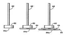
- a stacking tip 60is used to facilitate a top-down stacking technique.
- the stacking tip 60may be connected to a vacuum or suction hose (not shown), for example, to provide enough suction to lift one or more die securely.
- FIG. 4Aillustrates the stacking tip 60 after it has lifted a first die 62 .
- the first diemay advantageously include a layer of adhesive, such as paste or epoxy, on the underside 62 a .
- the stacking tip 60may be used to facilitate the dipping, brushing or spraying, for example, of the underside 62 a of the first die 60 with an adhesive after the first die 62 is lifted by the stacking tip 60 .
- FIG. 4Billustrates the stacking tip 60 after it has lifted a second die 64 .
- the stacking tip 60may be manually or automatically directed to the second die 64 . Regardless of the mechanism, by placing the underside 62 a of the first die 62 in contact with the second die 64 , the second die 64 is adhesively coupled to the first die 62 , thereby creating a stack of two die.
- the first die 62may be thicker than the second die 64 .
- the first die 62may, for example, have a thickness of 6-10 mils, while the second die 64 may have a thickness of 1-6 mils.
- the thicker diemay enhance the overall durability of the die stack as well as provide structural support during the die stacking process. However, in some applications, it may not be necessary or desirable to use die of varying thicknesses.
- the surface area of the first die 62may be smaller than the surface area of the second die 64 , and the first die 62 may be attached to the second die 64 such that the entire perimeter of the first die 62 is contained within the perimeter of the second die 64 .
- the second diemay advantageously include a layer of adhesive, such as paste or epoxy, on the underside 64 a to facilitate the adhesive attachment to a third die.
- the stackmay only include the first die 62 and the second die 64 .
- FIG. 4Cillustrates the stacking tip 60 after it has lifted a third die 66 .
- the stacking tip 60may be manually or automatically directed to the third die 66 .
- the third die 66is adhesively coupled to the second die 64 , thereby creating a stack of three die. If the die stack includes more than three die, the underside 66 a of the third die 66 may be coated with an adhesive to facilitate further die stacking. The process may be repeated a number of times depending on the number of die in the stack.
- the bottom die in the stackhere the third die 66 ) may not include an adhesive on the underside if further stacking is not desired.
- the completed die stackmay be deposited on a temporary holding surface such as a film frame, gel pack, tape reel, JEDEC tray, etc., for later attachment onto a substrate. Further, before the die stack is attached to the substrate, the die stack may be cured at a high temperature, in the range of 50-400° C., for example. Still further, prior to attachment to a substrate or even prior to attachment to the temporary holding surface, the die may be tested to ensure that all die in the stack are functional, thus forming a known good die stack (KGDS). The adhesive used to attach each die together may be different than the adhesive which may be used later to attach the die stack to the substrate. Once the die stack is coupled to a substrate using a second adhesive, the package may again be cured.
- KGDSknown good die stack
- the temperature used to cure the second adhesivemay be lower, thereby minimizing the effects of the CTE mismatch.
- the second adhesivemay be cured in the temperature range of 50-100° C., for example.
- the temporary holding surfacemay be a die wafer, wherein the die stack is deposited on top of a known good die which is still in wafer form.
- the known good die on which the die stack is depositedmay be adhesively attached to the die stack by an adhesive on the exposed underside of the die stack, as previously described, and the known good die will form the bottom die of the die stack.
- the holding surfaceis considered temporary in that the wafer itself may be used to temporarily hold, transfer, test or store one or more die stacks for example.
- the wafermay be uncut or cut. If the wafer is cut, it may include an adhesive backing, such as a tape, which holds the die in wafer form until the stacks are separated for curing, testing and/or attachment to a substrate.
- Each of the wafersis excised but may be held together by a tape backing, for instance, such that the individual die, preferably the known good die, can be lifted from the tape. If the wafer is uncut, the wafer will then be cut or otherwise separated prior to incorporation of the excised die stacks into packages. Stacks may be assembled across an entire wafer. Once the wafer is cut, the cut wafer with die stacks may be loaded into conventional die attach equipment for attachment to a substrate.
- One advantage of the technique of forming the entire stack prior to attaching it to the substrateis that the entire die stack is attached to the substrate with one motion thereby reducing the number of iterations as compared to the typical method of forming die stacks directly on the substrate. As previously described, the prior stacking techniques may necessitate several iterations in the building of the die stacks directly on the substrate.
- FIG. 5Aillustrates a top plan view of an exemplary die stack 70 .
- a cross section of the die stack 70 taken along the line A—Ais illustrated in FIG. 5 B.
- the die stack 70includes a first die 72 , a second die 74 , and a third die 76 .
- each of the die in the die stack 70has approximately the same thickness, as illustrated in FIG. 5 B.
- the first die 72has a smaller topside surface area than the second die 74
- the second die 74has a smaller topside surface area than the third die 76 , as illustrated in FIG. 5 A.
- the die stackis configured such that the first die 72 is substantially centered within the perimeter of the second die 74 , and the second die 74 is substantially centered within the perimeter of the third die 76 .
- FIGS. 5C and 5Dare cross-sectional views of “shingle stacks.”
- Shingle stacksare die stacks wherein upper die may overhang die below them in the stack.
- FIG. 5Cillustrates one embodiment of a shingle stack 80 .
- the shingle stack 80includes a first die 82 , a second die 84 , and a third die 86 .
- the second die 84has been attached to the third die 86 such that the edge of the second die 84 overhangs the edge of the third die 86 .
- first die 82is attached to the second die 84 such that the edge of the first die 82 overhangs the edge of the second die 84 .
- the exemplary embodiment illustrated in FIG. 5Cincorporates die of the same size and thickness with respect to one another.
- FIG. 5Dillustrates an alternate embodiment of a shingle stack 90 .
- the shingle stack 90includes a first die 92 , a second die 94 and a third die 96 .
- the second die 94has been attached to the third die 96 such that the edge of the second die 94 overhangs the edge of the third die 96 .
- the first die 92is attached to the second die 94 such that the edge of the first die 92 is relatively even with the edge of the third die 96 .
- the exemplary embodiment illustrated in FIG. 5Dincorporates die of the same thickness with respect to one another but differing in size.
- the embodiment illustrated in FIG. 5Dcan be viewed as a hybrid of the embodiments illustrated in FIGS. 5B and 5C.
- Various configurations and dimensions of die and die stacksmay be advantageous in various applications and may be implemented in accordance with the present techniques.
- FIG. 6illustrates a block diagram of an exemplary assembly system 100 in accordance with the present techniques.
- the system 100may include an assembly table 102 on which the pre-stacked die may be disposed.
- each of the die which will be used to build a die stackare contained within one of a first wafer 104 , a second wafer 106 , and a third wafer 108 .
- Each of the wafersis excised but may be held together by a tape backing, for instance, such that the individual die, preferably the known good die, can be lifted from the tape by the stacking tip 110 .
- three containers or die packs containing excised diemay be placed on the assembly table 102 in place of the wafers.
- the stacking tip 110maybe attached to a vacuum hose 112 to provide a suction at the end of the stacking tip 110 to facilitate the lifting of one or more die.
- the suction provided through the stacking tip 110is advantageously at such a strength as to facilitate the separation of the individual die from their corresponding wafers 104 , 106 and 108 (or containers) and to lift the die (or plurality of stacked die) which will be used to form the die stack.
- the stacking tip 110may include a gripping structure 114 to facilitate manual operation of the stacking tip 110 .
- a first diemay be lifted from the first wafer 104 using the stacking tip 110 .
- the die from the first wafer 104(“first die”) may have an adhesive coating on the underside of the die or may be coated with an adhesive after the first die is removed from the first wafer 104 .
- the stacking tip 110is used to manipulate the first die on top of a die on the second wafer 106 (“second die”).
- the adhesive on the underside of the first diewill facilitate the coupling of the first die to the second die as the first die is pressed against the second die.
- the stack, including the first and second die,is lifted from the second wafer 106 .
- the second diemay have an adhesive coating on the underside of the die or may be coated with an adhesive after the second die is removed from the second wafer 106 .
- the stacking tip 100is used to manipulate the stack (including the first and second die) on top of a die on the third wafer 108 (“third die”).
- the adhesive on the underside of the second diewill facilitate the coupling of the second die to the third die as the stack is pressed against the third die.
- the die stackmay then be lifted and disposed on a temporary holding surface 116 , such as a gel pack, film frame, etc. to await further processing.
- the aforementioned processmay be repeated until one of the wafers 104 , 106 or 108 has been depleted of its die supply. At that point, another wafer may be removed from a respective wafer tray 118 , 120 or 122 and placed on the assembly table 102 for continued stack assembly. It should be noted that the thickness and dimensions of each of the corresponding wafers 104 , 106 and 108 may vary as previously described with references to FIGS. 4 and 5. Further, as described with reference to FIG. 5, the stacking configuration may vary depending on system requirements or user preferences.
- the diemay be stacked on a temporary holding surface such as a gel pack, film frame, tape reel etc., or a wafer wherein the known good die on the wafer are used as the bottom die in the stacks. In the latter embodiment, the die stacks are formed directly on the known good die on the wafer.
- a stacking tipmay be used to stack the die on the wafer or other temporary holding surface.
- the die stacksare formed by a top-down technique or alternately by a bottom-up technique
- one of the advantages of the present systemis the formation of the die stack without a substrate.
- the stackcan be assembled using a first adhesive and cured at a different temperature than the adhesive later used to attach the die stack to a substrate, as discussed above.
- the die stackcan be electrically tested prior to attachment to a substrate. By identifying bad die stacks before attaching them to a substrate, unnecessary scrapping of good substrates may be avoided.
- the die stackcan be mechanically and structurally tested for functionality and/or reliability.
- functional testingcan be used to screen die stacks before they are attached to a corresponding substrate.
- Faulty die stackscan be identified and scrapped prior to substrate attachment.
- Typical environmental and structural testingmay include thermal cycling, temperature cycling, autoclave, vibration testing, etc.
- the die stacksmay be attached to a substrate to form a package, such as those illustrated with reference to FIGS. 2 and 3.
Landscapes
- Engineering & Computer Science (AREA)
- Microelectronics & Electronic Packaging (AREA)
- Power Engineering (AREA)
- Physics & Mathematics (AREA)
- Condensed Matter Physics & Semiconductors (AREA)
- General Physics & Mathematics (AREA)
- Computer Hardware Design (AREA)
- Manufacturing & Machinery (AREA)
- Container, Conveyance, Adherence, Positioning, Of Wafer (AREA)
Abstract
Description
Claims (11)
Priority Applications (7)
| Application Number | Priority Date | Filing Date | Title |
|---|---|---|---|
| US10/141,447US6682955B2 (en) | 2002-05-08 | 2002-05-08 | Stacked die module and techniques for forming a stacked die module |
| US10/672,750US7755204B2 (en) | 2002-05-08 | 2003-09-25 | Stacked die module including multiple adhesives that cure at different temperatures |
| US10/770,941US7217596B2 (en) | 2002-05-08 | 2004-02-03 | Stacked die module and techniques for forming a stacked die module |
| US10/770,919US20040154956A1 (en) | 2002-05-08 | 2004-02-03 | Stacked die module and techniques for forming a stacked die module |
| US10/771,243US20040155327A1 (en) | 2002-05-08 | 2004-02-03 | Stacked die module and techniques for forming a stacked die module |
| US10/771,085US7029931B2 (en) | 2002-05-08 | 2004-02-03 | Stacked die module and techniques for forming a stacked die module |
| US11/266,972US7186576B2 (en) | 2002-05-08 | 2005-11-04 | Stacked die module and techniques for forming a stacked die module |
Applications Claiming Priority (1)
| Application Number | Priority Date | Filing Date | Title |
|---|---|---|---|
| US10/141,447US6682955B2 (en) | 2002-05-08 | 2002-05-08 | Stacked die module and techniques for forming a stacked die module |
Related Child Applications (1)
| Application Number | Title | Priority Date | Filing Date |
|---|---|---|---|
| US10/672,750DivisionUS7755204B2 (en) | 2002-05-08 | 2003-09-25 | Stacked die module including multiple adhesives that cure at different temperatures |
Publications (2)
| Publication Number | Publication Date |
|---|---|
| US20030211655A1 US20030211655A1 (en) | 2003-11-13 |
| US6682955B2true US6682955B2 (en) | 2004-01-27 |
Family
ID=29399665
Family Applications (7)
| Application Number | Title | Priority Date | Filing Date |
|---|---|---|---|
| US10/141,447Expired - LifetimeUS6682955B2 (en) | 2002-05-08 | 2002-05-08 | Stacked die module and techniques for forming a stacked die module |
| US10/672,750Expired - LifetimeUS7755204B2 (en) | 2002-05-08 | 2003-09-25 | Stacked die module including multiple adhesives that cure at different temperatures |
| US10/770,941Expired - LifetimeUS7217596B2 (en) | 2002-05-08 | 2004-02-03 | Stacked die module and techniques for forming a stacked die module |
| US10/770,919AbandonedUS20040154956A1 (en) | 2002-05-08 | 2004-02-03 | Stacked die module and techniques for forming a stacked die module |
| US10/771,243AbandonedUS20040155327A1 (en) | 2002-05-08 | 2004-02-03 | Stacked die module and techniques for forming a stacked die module |
| US10/771,085Expired - LifetimeUS7029931B2 (en) | 2002-05-08 | 2004-02-03 | Stacked die module and techniques for forming a stacked die module |
| US11/266,972Expired - LifetimeUS7186576B2 (en) | 2002-05-08 | 2005-11-04 | Stacked die module and techniques for forming a stacked die module |
Family Applications After (6)
| Application Number | Title | Priority Date | Filing Date |
|---|---|---|---|
| US10/672,750Expired - LifetimeUS7755204B2 (en) | 2002-05-08 | 2003-09-25 | Stacked die module including multiple adhesives that cure at different temperatures |
| US10/770,941Expired - LifetimeUS7217596B2 (en) | 2002-05-08 | 2004-02-03 | Stacked die module and techniques for forming a stacked die module |
| US10/770,919AbandonedUS20040154956A1 (en) | 2002-05-08 | 2004-02-03 | Stacked die module and techniques for forming a stacked die module |
| US10/771,243AbandonedUS20040155327A1 (en) | 2002-05-08 | 2004-02-03 | Stacked die module and techniques for forming a stacked die module |
| US10/771,085Expired - LifetimeUS7029931B2 (en) | 2002-05-08 | 2004-02-03 | Stacked die module and techniques for forming a stacked die module |
| US11/266,972Expired - LifetimeUS7186576B2 (en) | 2002-05-08 | 2005-11-04 | Stacked die module and techniques for forming a stacked die module |
Country Status (1)
| Country | Link |
|---|---|
| US (7) | US6682955B2 (en) |
Cited By (8)
| Publication number | Priority date | Publication date | Assignee | Title |
|---|---|---|---|---|
| US20040056342A1 (en)* | 2002-05-08 | 2004-03-25 | Cobbley Chad A. | Stacked die module and techniques for forming a stacked die module |
| US20050073045A1 (en)* | 2003-10-02 | 2005-04-07 | Interdigital Technology Corporation | Wireless coupling of stacked dies within system in package |
| US20070210447A1 (en)* | 2006-03-07 | 2007-09-13 | Kinsley Thomas H | Elongated fasteners for securing together electronic components and substrates, semiconductor device assemblies including such fasteners, and accompanying systems and methods |
| US20080032517A1 (en)* | 2006-08-01 | 2008-02-07 | General Dynamics Advanced Information Systems | Method and apparatus for compliantly connecting stack of high-density electronic modules in harsh environments |
| US20080237310A1 (en)* | 2007-03-26 | 2008-10-02 | Shanggar Periaman | Die backside wire bond technology for single or stacked die package |
| US20090065951A1 (en)* | 2007-09-10 | 2009-03-12 | Bok Eng Cheah | Stacked die package |
| US20110147917A1 (en)* | 2009-12-22 | 2011-06-23 | Fairchild Semiconductor Corporation | Integrated circuit package with embedded components |
| US20110163391A1 (en)* | 2010-01-06 | 2011-07-07 | Fairchild Semiconductor Corporation | Wafer level stack die package |
Families Citing this family (52)
| Publication number | Priority date | Publication date | Assignee | Title |
|---|---|---|---|---|
| US7388294B2 (en)* | 2003-01-27 | 2008-06-17 | Micron Technology, Inc. | Semiconductor components having stacked dice |
| JP2005045023A (en)* | 2003-07-22 | 2005-02-17 | Toshiba Corp | Semiconductor device manufacturing method and semiconductor manufacturing apparatus |
| US7091124B2 (en) | 2003-11-13 | 2006-08-15 | Micron Technology, Inc. | Methods for forming vias in microelectronic devices, and methods for packaging microelectronic devices |
| US8084866B2 (en) | 2003-12-10 | 2011-12-27 | Micron Technology, Inc. | Microelectronic devices and methods for filling vias in microelectronic devices |
| US20050247894A1 (en) | 2004-05-05 | 2005-11-10 | Watkins Charles M | Systems and methods for forming apertures in microfeature workpieces |
| US7232754B2 (en) | 2004-06-29 | 2007-06-19 | Micron Technology, Inc. | Microelectronic devices and methods for forming interconnects in microelectronic devices |
| US7425499B2 (en) | 2004-08-24 | 2008-09-16 | Micron Technology, Inc. | Methods for forming interconnects in vias and microelectronic workpieces including such interconnects |
| SG120200A1 (en)* | 2004-08-27 | 2006-03-28 | Micron Technology Inc | Slanted vias for electrical circuits on circuit boards and other substrates |
| US7300857B2 (en) | 2004-09-02 | 2007-11-27 | Micron Technology, Inc. | Through-wafer interconnects for photoimager and memory wafers |
| US7217995B2 (en)* | 2004-11-12 | 2007-05-15 | Macronix International Co., Ltd. | Apparatus for stacking electrical components using insulated and interconnecting via |
| US7271482B2 (en) | 2004-12-30 | 2007-09-18 | Micron Technology, Inc. | Methods for forming interconnects in microelectronic workpieces and microelectronic workpieces formed using such methods |
| US7795134B2 (en) | 2005-06-28 | 2010-09-14 | Micron Technology, Inc. | Conductive interconnect structures and formation methods using supercritical fluids |
| US7622377B2 (en)* | 2005-09-01 | 2009-11-24 | Micron Technology, Inc. | Microfeature workpiece substrates having through-substrate vias, and associated methods of formation |
| US7262134B2 (en) | 2005-09-01 | 2007-08-28 | Micron Technology, Inc. | Microfeature workpieces and methods for forming interconnects in microfeature workpieces |
| US7863187B2 (en) | 2005-09-01 | 2011-01-04 | Micron Technology, Inc. | Microfeature workpieces and methods for forming interconnects in microfeature workpieces |
| US20070152314A1 (en)* | 2005-12-30 | 2007-07-05 | Intel Corporation | Low stress stacked die packages |
| US7288835B2 (en)* | 2006-03-17 | 2007-10-30 | Stats Chippac Ltd. | Integrated circuit package-in-package system |
| US7749899B2 (en) | 2006-06-01 | 2010-07-06 | Micron Technology, Inc. | Microelectronic workpieces and methods and systems for forming interconnects in microelectronic workpieces |
| WO2008014633A1 (en)* | 2006-06-29 | 2008-02-07 | Intel Corporation | Apparatus, system, and method for wireless connection in integrated circuit packages |
| US7629249B2 (en)* | 2006-08-28 | 2009-12-08 | Micron Technology, Inc. | Microfeature workpieces having conductive interconnect structures formed by chemically reactive processes, and associated systems and methods |
| US7723833B2 (en) | 2006-08-30 | 2010-05-25 | United Test And Assembly Center Ltd. | Stacked die packages |
| US7902643B2 (en) | 2006-08-31 | 2011-03-08 | Micron Technology, Inc. | Microfeature workpieces having interconnects and conductive backplanes, and associated systems and methods |
| US7477535B2 (en)* | 2006-10-05 | 2009-01-13 | Nokia Corporation | 3D chip arrangement including memory manager |
| US20080086603A1 (en)* | 2006-10-05 | 2008-04-10 | Vesa Lahtinen | Memory management method and system |
| US8110899B2 (en)* | 2006-12-20 | 2012-02-07 | Intel Corporation | Method for incorporating existing silicon die into 3D integrated stack |
| TWI376662B (en)* | 2007-05-03 | 2012-11-11 | Novatek Microelectronics Corp | Apparatus for controlling the liquid crystal display |
| US8367471B2 (en)* | 2007-06-15 | 2013-02-05 | Micron Technology, Inc. | Semiconductor assemblies, stacked semiconductor devices, and methods of manufacturing semiconductor assemblies and stacked semiconductor devices |
| SG149710A1 (en) | 2007-07-12 | 2009-02-27 | Micron Technology Inc | Interconnects for packaged semiconductor devices and methods for manufacturing such devices |
| SG149724A1 (en)* | 2007-07-24 | 2009-02-27 | Micron Technology Inc | Semicoductor dies with recesses, associated leadframes, and associated systems and methods |
| SG149725A1 (en) | 2007-07-24 | 2009-02-27 | Micron Technology Inc | Thin semiconductor die packages and associated systems and methods |
| SG150410A1 (en) | 2007-08-31 | 2009-03-30 | Micron Technology Inc | Partitioned through-layer via and associated systems and methods |
| US7816934B2 (en)* | 2007-10-16 | 2010-10-19 | Micron Technology, Inc. | Reconfigurable connections for stacked semiconductor devices |
| US7829379B2 (en)* | 2007-10-17 | 2010-11-09 | Analog Devices, Inc. | Wafer level stacked die packaging |
| US7884015B2 (en) | 2007-12-06 | 2011-02-08 | Micron Technology, Inc. | Methods for forming interconnects in microelectronic workpieces and microelectronic workpieces formed using such methods |
| US8084854B2 (en) | 2007-12-28 | 2011-12-27 | Micron Technology, Inc. | Pass-through 3D interconnect for microelectronic dies and associated systems and methods |
| US7821107B2 (en)* | 2008-04-22 | 2010-10-26 | Micron Technology, Inc. | Die stacking with an annular via having a recessed socket |
| US8253230B2 (en) | 2008-05-15 | 2012-08-28 | Micron Technology, Inc. | Disabling electrical connections using pass-through 3D interconnects and associated systems and methods |
| WO2009153714A1 (en)* | 2008-06-16 | 2009-12-23 | Nxp B.V. | Voltage converter |
| US7800238B2 (en)* | 2008-06-27 | 2010-09-21 | Micron Technology, Inc. | Surface depressions for die-to-die interconnects and associated systems and methods |
| US8399974B1 (en)* | 2008-07-10 | 2013-03-19 | Henkel Corporation | Methods of dicing stacked shingled strip constructions to form stacked die packages |
| JP2010192680A (en)* | 2009-02-18 | 2010-09-02 | Elpida Memory Inc | Semiconductor device |
| US8541886B2 (en)* | 2010-03-09 | 2013-09-24 | Stats Chippac Ltd. | Integrated circuit packaging system with via and method of manufacture thereof |
| US8542030B2 (en)* | 2010-11-09 | 2013-09-24 | International Business Machines Corporation | Three-dimensional (3D) stacked integrated circuit testing |
| US9824906B2 (en) | 2013-09-03 | 2017-11-21 | Altera Corporation | Methods and structures for handling integrated circuits |
| US11171115B2 (en) | 2019-03-18 | 2021-11-09 | Kepler Computing Inc. | Artificial intelligence processor with three-dimensional stacked memory |
| US11836102B1 (en) | 2019-03-20 | 2023-12-05 | Kepler Computing Inc. | Low latency and high bandwidth artificial intelligence processor |
| CN111834438B (en)* | 2019-04-18 | 2024-05-31 | 西部数据技术公司 | Hole structure on the back side of semiconductor components for mitigating delamination in stacked packages |
| US12079475B1 (en) | 2019-05-31 | 2024-09-03 | Kepler Computing Inc. | Ferroelectric memory chiplet in a multi-dimensional packaging |
| US11043472B1 (en) | 2019-05-31 | 2021-06-22 | Kepler Compute Inc. | 3D integrated ultra high-bandwidth memory |
| US11844223B1 (en) | 2019-05-31 | 2023-12-12 | Kepler Computing Inc. | Ferroelectric memory chiplet as unified memory in a multi-dimensional packaging |
| US12086410B1 (en) | 2019-05-31 | 2024-09-10 | Kepler Computing Inc. | Ferroelectric memory chiplet in a multi-dimensional packaging with I/O switch embedded in a substrate or interposer |
| US11791233B1 (en) | 2021-08-06 | 2023-10-17 | Kepler Computing Inc. | Ferroelectric or paraelectric memory and logic chiplet with thermal management in a multi-dimensional packaging |
Citations (10)
| Publication number | Priority date | Publication date | Assignee | Title |
|---|---|---|---|---|
| US6064120A (en) | 1997-08-21 | 2000-05-16 | Micron Technology, Inc. | Apparatus and method for face-to-face connection of a die face to a substrate with polymer electrodes |
| US6184064B1 (en) | 2000-01-12 | 2001-02-06 | Micron Technology, Inc. | Semiconductor die back side surface and method of fabrication |
| US6285081B1 (en) | 1999-07-13 | 2001-09-04 | Micron Technology, Inc. | Deflectable interconnect |
| US6329220B1 (en) | 1999-11-23 | 2001-12-11 | Micron Technology, Inc. | Packages for semiconductor die |
| US6331221B1 (en) | 1998-04-15 | 2001-12-18 | Micron Technology, Inc. | Process for providing electrical connection between a semiconductor die and a semiconductor die receiving member |
| US6343019B1 (en) | 1997-12-22 | 2002-01-29 | Micron Technology, Inc. | Apparatus and method of stacking die on a substrate |
| US6353268B1 (en) | 1997-08-22 | 2002-03-05 | Micron Technology, Inc. | Semiconductor die attachment method and apparatus |
| US6387728B1 (en)* | 1999-11-09 | 2002-05-14 | Advanced Semiconductor Engineering, Inc. | Method for fabricating a stacked chip package |
| US6503776B2 (en)* | 2001-01-05 | 2003-01-07 | Advanced Semiconductor Engineering, Inc. | Method for fabricating stacked chip package |
| US6586825B1 (en)* | 2001-04-26 | 2003-07-01 | Lsi Logic Corporation | Dual chip in package with a wire bonded die mounted to a substrate |
Family Cites Families (64)
| Publication number | Priority date | Publication date | Assignee | Title |
|---|---|---|---|---|
| US1835350A (en) | 1929-07-30 | 1931-12-08 | Alberta L Soffel | Display cabinet |
| US4285433A (en) | 1979-12-19 | 1981-08-25 | Western Electric Co., Inc. | Method and apparatus for removing dice from a severed wafer |
| JPS5715455A (en) | 1980-07-01 | 1982-01-26 | Fujitsu Ltd | Semiconductor device |
| US4589547A (en) | 1983-01-14 | 1986-05-20 | Motorola Inc. | Carrier for stacked semiconductor die |
| JPS6010634A (en) | 1983-06-30 | 1985-01-19 | Nec Kyushu Ltd | Automatic sorter in semiconductor element manufacturing apparatus |
| JPS6248037A (en) | 1985-08-28 | 1987-03-02 | Toshiba Corp | Conveyor of diced wafer |
| JPH01108008A (en) | 1987-10-21 | 1989-04-25 | Matsushita Electric Ind Co Ltd | Cutting of semiconducting wafers |
| US5145099A (en) | 1990-07-13 | 1992-09-08 | Micron Technology, Inc. | Method for combining die attach and lead bond in the assembly of a semiconductor package |
| US5199564A (en)* | 1992-03-13 | 1993-04-06 | Minnesota Mining And Manufacturing Company | Carrier tape for electronic through-hole components |
| US5477160A (en) | 1992-08-12 | 1995-12-19 | Fujitsu Limited | Module test card |
| JP2991398B2 (en) | 1993-11-12 | 1999-12-20 | 株式会社トーショー | Preparation method of injection medicine |
| US5828224A (en) | 1994-03-18 | 1998-10-27 | Fujitsu, Limited | Test carrier for semiconductor integrated circuit and method of testing semiconductor integrated circuit |
| US5891761A (en) | 1994-06-23 | 1999-04-06 | Cubic Memory, Inc. | Method for forming vertical interconnect process for silicon segments with thermally conductive epoxy preform |
| US5675180A (en) | 1994-06-23 | 1997-10-07 | Cubic Memory, Inc. | Vertical interconnect process for silicon segments |
| JPH09113577A (en) | 1995-10-20 | 1997-05-02 | Toshiba Corp | Semiconductor chip characteristic evaluation board and chip mounting method |
| US5719440A (en)* | 1995-12-19 | 1998-02-17 | Micron Technology, Inc. | Flip chip adaptor package for bare die |
| US5952725A (en) | 1996-02-20 | 1999-09-14 | Micron Technology, Inc. | Stacked semiconductor devices |
| US7166495B2 (en) | 1996-02-20 | 2007-01-23 | Micron Technology, Inc. | Method of fabricating a multi-die semiconductor package assembly |
| US5696031A (en) | 1996-11-20 | 1997-12-09 | Micron Technology, Inc. | Device and method for stacking wire-bonded integrated circuit dice on flip-chip bonded integrated circuit dice |
| US6784023B2 (en) | 1996-05-20 | 2004-08-31 | Micron Technology, Inc. | Method of fabrication of stacked semiconductor devices |
| DE19626126C2 (en) | 1996-06-28 | 1998-04-16 | Fraunhofer Ges Forschung | Method for forming a spatial chip arrangement and spatial chip arrangement |
| US6274389B1 (en)* | 1997-01-17 | 2001-08-14 | Loctite (R&D) Ltd. | Mounting structure and mounting process from semiconductor devices |
| US6028437A (en) | 1997-05-19 | 2000-02-22 | Si Diamond Technology, Inc. | Probe head assembly |
| KR100278137B1 (en) | 1997-09-04 | 2001-01-15 | 가나이 쓰도무 | Method of mounting semiconductor device and system thereof, method of manufacturing semiconductor device isolator and IC card |
| EP0942460A1 (en)* | 1998-03-13 | 1999-09-15 | STMicroelectronics SA | Process for forming a low resistive Titanum silicide layer on a semiconductor substrate and device obtained thereby |
| US5854507A (en)* | 1998-07-21 | 1998-12-29 | Hewlett-Packard Company | Multiple chip assembly |
| FR2781925B1 (en) | 1998-07-30 | 2001-11-23 | Commissariat Energie Atomique | SELECTIVE TRANSFER OF ELEMENTS FROM ONE MEDIUM TO ANOTHER MEDIUM |
| US6660643B1 (en)* | 1999-03-03 | 2003-12-09 | Rwe Schott Solar, Inc. | Etching of semiconductor wafer edges |
| TW404030B (en)* | 1999-04-12 | 2000-09-01 | Siliconware Precision Industries Co Ltd | Dual-chip semiconductor package device having malposition and the manufacture method thereof |
| JP3368876B2 (en) | 1999-11-05 | 2003-01-20 | 株式会社東京精密 | Semiconductor chip manufacturing method |
| US6214733B1 (en) | 1999-11-17 | 2001-04-10 | Elo Technologies, Inc. | Process for lift off and handling of thin film materials |
| US6400173B1 (en) | 1999-11-19 | 2002-06-04 | Hitachi, Ltd. | Test system and manufacturing of semiconductor device |
| DE19961791C2 (en) | 1999-12-21 | 2002-11-28 | Infineon Technologies Ag | Arrangement for testing chips using a printed circuit board |
| US6605875B2 (en)* | 1999-12-30 | 2003-08-12 | Intel Corporation | Integrated circuit die having bond pads near adjacent sides to allow stacking of dice without regard to dice size |
| US6474475B1 (en) | 2000-02-22 | 2002-11-05 | Micron Technology, Inc. | Apparatus for handling stacked integrated circuit devices |
| US6337225B1 (en)* | 2000-03-30 | 2002-01-08 | Advanced Micro Devices, Inc. | Method of making stacked die assemblies and modules |
| US20020058357A1 (en)* | 2000-05-16 | 2002-05-16 | Siliconware Precision Industries Co., Ltd. | Die attaching method |
| US6426552B1 (en)* | 2000-05-19 | 2002-07-30 | Micron Technology, Inc. | Methods employing hybrid adhesive materials to secure components of semiconductor device assemblies and packages to one another and assemblies and packages including components secured to one another with such hybrid adhesive materials |
| US6258626B1 (en)* | 2000-07-06 | 2001-07-10 | Advanced Semiconductor Engineering, Inc. | Method of making stacked chip package |
| US6562648B1 (en) | 2000-08-23 | 2003-05-13 | Xerox Corporation | Structure and method for separation and transfer of semiconductor thin films onto dissimilar substrate materials |
| US6627477B1 (en)* | 2000-09-07 | 2003-09-30 | International Business Machines Corporation | Method of assembling a plurality of semiconductor devices having different thickness |
| JP3822043B2 (en) | 2000-09-25 | 2006-09-13 | 太陽誘電株式会社 | Chip part assembly manufacturing method |
| EP1399583A4 (en)* | 2000-10-27 | 2004-09-08 | Diadexus Inc | Compositions and methods relating to breast specific genes and proteins |
| JP4803884B2 (en) | 2001-01-31 | 2011-10-26 | キヤノン株式会社 | Method for manufacturing thin film semiconductor device |
| JP3419398B2 (en)* | 2001-02-23 | 2003-06-23 | 松下電器産業株式会社 | Method for manufacturing semiconductor device |
| FR2823012B1 (en) | 2001-04-03 | 2004-05-21 | Commissariat Energie Atomique | METHOD FOR SELECTIVELY TRANSFERRING AT LEAST ONE ELEMENT OF AN INITIAL MEDIUM ON A FINAL MEDIUM |
| JP3839323B2 (en)* | 2001-04-06 | 2006-11-01 | 株式会社ルネサステクノロジ | Manufacturing method of semiconductor device |
| US6599764B1 (en) | 2001-05-30 | 2003-07-29 | Altera Corporation | Isolation testing scheme for multi-die packages |
| US6900528B2 (en)* | 2001-06-21 | 2005-05-31 | Micron Technology, Inc. | Stacked mass storage flash memory package |
| US20030042615A1 (en) | 2001-08-30 | 2003-03-06 | Tongbi Jiang | Stacked microelectronic devices and methods of fabricating same |
| JP4800524B2 (en) | 2001-09-10 | 2011-10-26 | ルネサスエレクトロニクス株式会社 | Semiconductor device manufacturing method and manufacturing apparatus |
| US6787916B2 (en) | 2001-09-13 | 2004-09-07 | Tru-Si Technologies, Inc. | Structures having a substrate with a cavity and having an integrated circuit bonded to a contact pad located in the cavity |
| US6847105B2 (en) | 2001-09-21 | 2005-01-25 | Micron Technology, Inc. | Bumping technology in stacked die configurations |
| US6569709B2 (en)* | 2001-10-15 | 2003-05-27 | Micron Technology, Inc. | Assemblies including stacked semiconductor devices separated a distance defined by adhesive material interposed therebetween, packages including the assemblies, and methods |
| US20030122236A1 (en)* | 2002-01-02 | 2003-07-03 | Shibaek Nam | Semiconductor device having multi-chip package structure |
| US6774475B2 (en) | 2002-01-24 | 2004-08-10 | International Business Machines Corporation | Vertically stacked memory chips in FBGA packages |
| DE10208757B4 (en) | 2002-02-28 | 2006-06-29 | Infineon Technologies Ag | Method and magazine device for testing semiconductor devices |
| US20030178715A1 (en) | 2002-03-20 | 2003-09-25 | Bae Systems | Method for stacking chips within a multichip module package |
| US6867500B2 (en)* | 2002-04-08 | 2005-03-15 | Micron Technology, Inc. | Multi-chip module and methods |
| US6752205B2 (en)* | 2002-04-17 | 2004-06-22 | Tam International, Inc. | Inflatable packer with prestressed bladder |
| US6682955B2 (en) | 2002-05-08 | 2004-01-27 | Micron Technology, Inc. | Stacked die module and techniques for forming a stacked die module |
| JP2004047691A (en) | 2002-07-11 | 2004-02-12 | Seiko Epson Corp | Semiconductor device manufacturing method, electro-optical device, and electronic apparatus |
| KR100468748B1 (en)* | 2002-07-12 | 2005-01-29 | 삼성전자주식회사 | Dicing tape mounter applicable a pre-cut dicing tape and general dicing tape and In-line system having the dicing tape mounter |
| US7061099B2 (en)* | 2004-09-30 | 2006-06-13 | Intel Corporation | Microelectronic package having chamber sealed by material including one or more intermetallic compounds |
- 2002
- 2002-05-08USUS10/141,447patent/US6682955B2/ennot_activeExpired - Lifetime
- 2003
- 2003-09-25USUS10/672,750patent/US7755204B2/ennot_activeExpired - Lifetime
- 2004
- 2004-02-03USUS10/770,941patent/US7217596B2/ennot_activeExpired - Lifetime
- 2004-02-03USUS10/770,919patent/US20040154956A1/ennot_activeAbandoned
- 2004-02-03USUS10/771,243patent/US20040155327A1/ennot_activeAbandoned
- 2004-02-03USUS10/771,085patent/US7029931B2/ennot_activeExpired - Lifetime
- 2005
- 2005-11-04USUS11/266,972patent/US7186576B2/ennot_activeExpired - Lifetime
Patent Citations (10)
| Publication number | Priority date | Publication date | Assignee | Title |
|---|---|---|---|---|
| US6064120A (en) | 1997-08-21 | 2000-05-16 | Micron Technology, Inc. | Apparatus and method for face-to-face connection of a die face to a substrate with polymer electrodes |
| US6353268B1 (en) | 1997-08-22 | 2002-03-05 | Micron Technology, Inc. | Semiconductor die attachment method and apparatus |
| US6343019B1 (en) | 1997-12-22 | 2002-01-29 | Micron Technology, Inc. | Apparatus and method of stacking die on a substrate |
| US6331221B1 (en) | 1998-04-15 | 2001-12-18 | Micron Technology, Inc. | Process for providing electrical connection between a semiconductor die and a semiconductor die receiving member |
| US6285081B1 (en) | 1999-07-13 | 2001-09-04 | Micron Technology, Inc. | Deflectable interconnect |
| US6387728B1 (en)* | 1999-11-09 | 2002-05-14 | Advanced Semiconductor Engineering, Inc. | Method for fabricating a stacked chip package |
| US6329220B1 (en) | 1999-11-23 | 2001-12-11 | Micron Technology, Inc. | Packages for semiconductor die |
| US6184064B1 (en) | 2000-01-12 | 2001-02-06 | Micron Technology, Inc. | Semiconductor die back side surface and method of fabrication |
| US6503776B2 (en)* | 2001-01-05 | 2003-01-07 | Advanced Semiconductor Engineering, Inc. | Method for fabricating stacked chip package |
| US6586825B1 (en)* | 2001-04-26 | 2003-07-01 | Lsi Logic Corporation | Dual chip in package with a wire bonded die mounted to a substrate |
Cited By (25)
| Publication number | Priority date | Publication date | Assignee | Title |
|---|---|---|---|---|
| US20040056342A1 (en)* | 2002-05-08 | 2004-03-25 | Cobbley Chad A. | Stacked die module and techniques for forming a stacked die module |
| US20040155327A1 (en)* | 2002-05-08 | 2004-08-12 | Cobbley Chad A. | Stacked die module and techniques for forming a stacked die module |
| US20040154956A1 (en)* | 2002-05-08 | 2004-08-12 | Cobbley Chad A. | Stacked die module and techniques for forming a stacked die module |
| US7755204B2 (en) | 2002-05-08 | 2010-07-13 | Micron Technology, Inc. | Stacked die module including multiple adhesives that cure at different temperatures |
| US20050073045A1 (en)* | 2003-10-02 | 2005-04-07 | Interdigital Technology Corporation | Wireless coupling of stacked dies within system in package |
| US6953994B2 (en) | 2003-10-02 | 2005-10-11 | Interdigital Technology Corporation | Wireless coupling of staked dies within system in package |
| US20050253225A1 (en)* | 2003-10-02 | 2005-11-17 | Interdigital Technology Corporation | Wireless coupling of semiconductor dies |
| US7304374B2 (en) | 2003-10-02 | 2007-12-04 | Interdigital Technology Corporation | Wireless coupling of semiconductor dies |
| US20070210447A1 (en)* | 2006-03-07 | 2007-09-13 | Kinsley Thomas H | Elongated fasteners for securing together electronic components and substrates, semiconductor device assemblies including such fasteners, and accompanying systems and methods |
| US8124456B2 (en) | 2006-03-07 | 2012-02-28 | Micron Technology, Inc. | Methods for securing semiconductor devices using elongated fasteners |
| US20100112754A1 (en)* | 2006-03-07 | 2010-05-06 | Micron Technology, Inc. | Methods for securing semiconductor devices using elongated fasteners |
| US7663232B2 (en) | 2006-03-07 | 2010-02-16 | Micron Technology, Inc. | Elongated fasteners for securing together electronic components and substrates, semiconductor device assemblies including such fasteners, and accompanying systems |
| US20090246984A1 (en)* | 2006-08-01 | 2009-10-01 | Deepak Pai | Method and apparatus for compliantly connecting stack of high-density electronic modules in harsh environments |
| US7503767B2 (en) | 2006-08-01 | 2009-03-17 | General Dynamics Advanced Information Systems, Inc. | Method and apparatus for compliantly connecting stack of high-density electronic modules in harsh environments |
| US7818879B2 (en) | 2006-08-01 | 2010-10-26 | General Dynamics Advanced Information Systems, Inc. | Method and apparatus for compliantly connecting stack of high-density electronic modules in harsh environments |
| US20080032517A1 (en)* | 2006-08-01 | 2008-02-07 | General Dynamics Advanced Information Systems | Method and apparatus for compliantly connecting stack of high-density electronic modules in harsh environments |
| US20080237310A1 (en)* | 2007-03-26 | 2008-10-02 | Shanggar Periaman | Die backside wire bond technology for single or stacked die package |
| US8198716B2 (en) | 2007-03-26 | 2012-06-12 | Intel Corporation | Die backside wire bond technology for single or stacked die package |
| US20090065951A1 (en)* | 2007-09-10 | 2009-03-12 | Bok Eng Cheah | Stacked die package |
| US8044497B2 (en)* | 2007-09-10 | 2011-10-25 | Intel Corporation | Stacked die package |
| US20110147917A1 (en)* | 2009-12-22 | 2011-06-23 | Fairchild Semiconductor Corporation | Integrated circuit package with embedded components |
| US8304888B2 (en) | 2009-12-22 | 2012-11-06 | Fairchild Semiconductor Corporation | Integrated circuit package with embedded components |
| US20110163391A1 (en)* | 2010-01-06 | 2011-07-07 | Fairchild Semiconductor Corporation | Wafer level stack die package |
| US8115260B2 (en) | 2010-01-06 | 2012-02-14 | Fairchild Semiconductor Corporation | Wafer level stack die package |
| US8211747B2 (en) | 2010-01-06 | 2012-07-03 | Fairchild Semiconductor Corporation | Wafer level stack die package |
Also Published As
| Publication number | Publication date |
|---|---|
| US20040157373A1 (en) | 2004-08-12 |
| US20040154722A1 (en) | 2004-08-12 |
| US7755204B2 (en) | 2010-07-13 |
| US20040056342A1 (en) | 2004-03-25 |
| US20060063283A1 (en) | 2006-03-23 |
| US7186576B2 (en) | 2007-03-06 |
| US7029931B2 (en) | 2006-04-18 |
| US20040154956A1 (en) | 2004-08-12 |
| US20030211655A1 (en) | 2003-11-13 |
| US7217596B2 (en) | 2007-05-15 |
| US20040155327A1 (en) | 2004-08-12 |
Similar Documents
| Publication | Publication Date | Title |
|---|---|---|
| US6682955B2 (en) | Stacked die module and techniques for forming a stacked die module | |
| US6914326B2 (en) | Solder ball landpad design to improve laminate performance | |
| US7674652B2 (en) | Methods of forming an integrated circuit package | |
| US7663217B2 (en) | Semiconductor device package | |
| KR20110123204A (en) | Chip unit and manufacturing method thereof and stack package having same | |
| US20090321950A1 (en) | Stacked semiconductor package with localized cavities for wire bonding | |
| KR100593703B1 (en) | Semiconductor chip stack package with dummy chips for reinforcing protrusion wire bonding structure | |
| TWI475606B (en) | Non-uniform vacuum profile die attach tip | |
| US20090325342A1 (en) | Method of fabricating stacked semiconductor package with localized cavities for wire bonding | |
| CN110233113A (en) | A kind of packaging method of chip | |
| US6486536B1 (en) | U-shape tape for BOC FBGA package to improve moldability | |
| US6787393B2 (en) | Semiconductor package including a double-faced semiconductor chip having integrated circuitry on both sides thereof and a method of fabricating the semiconductor package | |
| US6691406B2 (en) | Methods of die attachment for BOC and F/C surface mount | |
| US6577015B1 (en) | Partial slot cover for encapsulation process | |
| US20030096451A1 (en) | Bare chip mounting method and bare chip mounting system | |
| KR100520602B1 (en) | Stacking structure of semiconductor chip | |
| CN120261303A (en) | Packaging method for staggered stacked chips on a redistribution layer | |
| KR20020042958A (en) | Stack chip package | |
| KR100377466B1 (en) | lamination apparatus of circuit film for semiconductor package and its method | |
| JP2002353401A (en) | Die collet for chip adsorption and semiconductor manufacturing method | |
| KR20050038502A (en) | Manufacturing method for stack ship package |
Legal Events
| Date | Code | Title | Description |
|---|---|---|---|
| AS | Assignment | Owner name:MICRON TECHNOLOGY, INC., IDAHO Free format text:ASSIGNMENT OF ASSIGNORS INTEREST;ASSIGNORS:COBBLEY, CHAD A.;JACKSON, TIMOTHY L.;REEL/FRAME:012905/0018 Effective date:20020506 | |
| FEPP | Fee payment procedure | Free format text:PAYOR NUMBER ASSIGNED (ORIGINAL EVENT CODE: ASPN); ENTITY STATUS OF PATENT OWNER: LARGE ENTITY | |
| STCF | Information on status: patent grant | Free format text:PATENTED CASE | |
| FPAY | Fee payment | Year of fee payment:4 | |
| FPAY | Fee payment | Year of fee payment:8 | |
| FPAY | Fee payment | Year of fee payment:12 | |
| AS | Assignment | Owner name:U.S. BANK NATIONAL ASSOCIATION, AS COLLATERAL AGENT, CALIFORNIA Free format text:SECURITY INTEREST;ASSIGNOR:MICRON TECHNOLOGY, INC.;REEL/FRAME:038669/0001 Effective date:20160426 Owner name:U.S. BANK NATIONAL ASSOCIATION, AS COLLATERAL AGEN Free format text:SECURITY INTEREST;ASSIGNOR:MICRON TECHNOLOGY, INC.;REEL/FRAME:038669/0001 Effective date:20160426 | |
| AS | Assignment | Owner name:MORGAN STANLEY SENIOR FUNDING, INC., AS COLLATERAL AGENT, MARYLAND Free format text:PATENT SECURITY AGREEMENT;ASSIGNOR:MICRON TECHNOLOGY, INC.;REEL/FRAME:038954/0001 Effective date:20160426 Owner name:MORGAN STANLEY SENIOR FUNDING, INC., AS COLLATERAL Free format text:PATENT SECURITY AGREEMENT;ASSIGNOR:MICRON TECHNOLOGY, INC.;REEL/FRAME:038954/0001 Effective date:20160426 | |
| AS | Assignment | Owner name:U.S. BANK NATIONAL ASSOCIATION, AS COLLATERAL AGENT, CALIFORNIA Free format text:CORRECTIVE ASSIGNMENT TO CORRECT THE REPLACE ERRONEOUSLY FILED PATENT #7358718 WITH THE CORRECT PATENT #7358178 PREVIOUSLY RECORDED ON REEL 038669 FRAME 0001. ASSIGNOR(S) HEREBY CONFIRMS THE SECURITY INTEREST;ASSIGNOR:MICRON TECHNOLOGY, INC.;REEL/FRAME:043079/0001 Effective date:20160426 Owner name:U.S. BANK NATIONAL ASSOCIATION, AS COLLATERAL AGEN Free format text:CORRECTIVE ASSIGNMENT TO CORRECT THE REPLACE ERRONEOUSLY FILED PATENT #7358718 WITH THE CORRECT PATENT #7358178 PREVIOUSLY RECORDED ON REEL 038669 FRAME 0001. ASSIGNOR(S) HEREBY CONFIRMS THE SECURITY INTEREST;ASSIGNOR:MICRON TECHNOLOGY, INC.;REEL/FRAME:043079/0001 Effective date:20160426 | |
| AS | Assignment | Owner name:JPMORGAN CHASE BANK, N.A., AS COLLATERAL AGENT, ILLINOIS Free format text:SECURITY INTEREST;ASSIGNORS:MICRON TECHNOLOGY, INC.;MICRON SEMICONDUCTOR PRODUCTS, INC.;REEL/FRAME:047540/0001 Effective date:20180703 Owner name:JPMORGAN CHASE BANK, N.A., AS COLLATERAL AGENT, IL Free format text:SECURITY INTEREST;ASSIGNORS:MICRON TECHNOLOGY, INC.;MICRON SEMICONDUCTOR PRODUCTS, INC.;REEL/FRAME:047540/0001 Effective date:20180703 | |
| AS | Assignment | Owner name:MICRON TECHNOLOGY, INC., IDAHO Free format text:RELEASE BY SECURED PARTY;ASSIGNOR:U.S. BANK NATIONAL ASSOCIATION, AS COLLATERAL AGENT;REEL/FRAME:047243/0001 Effective date:20180629 | |
| AS | Assignment | Owner name:MICRON TECHNOLOGY, INC., IDAHO Free format text:RELEASE BY SECURED PARTY;ASSIGNOR:MORGAN STANLEY SENIOR FUNDING, INC., AS COLLATERAL AGENT;REEL/FRAME:050937/0001 Effective date:20190731 | |
| AS | Assignment | Owner name:MICRON SEMICONDUCTOR PRODUCTS, INC., IDAHO Free format text:RELEASE BY SECURED PARTY;ASSIGNOR:JPMORGAN CHASE BANK, N.A., AS COLLATERAL AGENT;REEL/FRAME:051028/0001 Effective date:20190731 Owner name:MICRON TECHNOLOGY, INC., IDAHO Free format text:RELEASE BY SECURED PARTY;ASSIGNOR:JPMORGAN CHASE BANK, N.A., AS COLLATERAL AGENT;REEL/FRAME:051028/0001 Effective date:20190731 |