US6681982B2 - Pillar connections for semiconductor chips and method of manufacture - Google Patents
Pillar connections for semiconductor chips and method of manufactureDownload PDFInfo
- Publication number
- US6681982B2 US6681982B2US10/170,089US17008902AUS6681982B2US 6681982 B2US6681982 B2US 6681982B2US 17008902 AUS17008902 AUS 17008902AUS 6681982 B2US6681982 B2US 6681982B2
- Authority
- US
- United States
- Prior art keywords
- solder
- microns
- pillar
- copper
- substrate
- Prior art date
- Legal status (The legal status is an assumption and is not a legal conclusion. Google has not performed a legal analysis and makes no representation as to the accuracy of the status listed.)
- Expired - Lifetime, expires
Links
Images


Classifications
- H—ELECTRICITY
- H01—ELECTRIC ELEMENTS
- H01L—SEMICONDUCTOR DEVICES NOT COVERED BY CLASS H10
- H01L24/00—Arrangements for connecting or disconnecting semiconductor or solid-state bodies; Methods or apparatus related thereto
- H01L24/01—Means for bonding being attached to, or being formed on, the surface to be connected, e.g. chip-to-package, die-attach, "first-level" interconnects; Manufacturing methods related thereto
- H01L24/10—Bump connectors ; Manufacturing methods related thereto
- H01L24/15—Structure, shape, material or disposition of the bump connectors after the connecting process
- H01L24/16—Structure, shape, material or disposition of the bump connectors after the connecting process of an individual bump connector
- H—ELECTRICITY
- H01—ELECTRIC ELEMENTS
- H01L—SEMICONDUCTOR DEVICES NOT COVERED BY CLASS H10
- H01L24/00—Arrangements for connecting or disconnecting semiconductor or solid-state bodies; Methods or apparatus related thereto
- H01L24/01—Means for bonding being attached to, or being formed on, the surface to be connected, e.g. chip-to-package, die-attach, "first-level" interconnects; Manufacturing methods related thereto
- H01L24/10—Bump connectors ; Manufacturing methods related thereto
- H01L24/11—Manufacturing methods
- H—ELECTRICITY
- H01—ELECTRIC ELEMENTS
- H01L—SEMICONDUCTOR DEVICES NOT COVERED BY CLASS H10
- H01L24/00—Arrangements for connecting or disconnecting semiconductor or solid-state bodies; Methods or apparatus related thereto
- H01L24/01—Means for bonding being attached to, or being formed on, the surface to be connected, e.g. chip-to-package, die-attach, "first-level" interconnects; Manufacturing methods related thereto
- H01L24/10—Bump connectors ; Manufacturing methods related thereto
- H01L24/12—Structure, shape, material or disposition of the bump connectors prior to the connecting process
- H—ELECTRICITY
- H01—ELECTRIC ELEMENTS
- H01L—SEMICONDUCTOR DEVICES NOT COVERED BY CLASS H10
- H01L2224/00—Indexing scheme for arrangements for connecting or disconnecting semiconductor or solid-state bodies and methods related thereto as covered by H01L24/00
- H01L2224/01—Means for bonding being attached to, or being formed on, the surface to be connected, e.g. chip-to-package, die-attach, "first-level" interconnects; Manufacturing methods related thereto
- H01L2224/02—Bonding areas; Manufacturing methods related thereto
- H01L2224/04—Structure, shape, material or disposition of the bonding areas prior to the connecting process
- H01L2224/05—Structure, shape, material or disposition of the bonding areas prior to the connecting process of an individual bonding area
- H01L2224/0554—External layer
- H01L2224/0556—Disposition
- H01L2224/05568—Disposition the whole external layer protruding from the surface
- H—ELECTRICITY
- H01—ELECTRIC ELEMENTS
- H01L—SEMICONDUCTOR DEVICES NOT COVERED BY CLASS H10
- H01L2224/00—Indexing scheme for arrangements for connecting or disconnecting semiconductor or solid-state bodies and methods related thereto as covered by H01L24/00
- H01L2224/01—Means for bonding being attached to, or being formed on, the surface to be connected, e.g. chip-to-package, die-attach, "first-level" interconnects; Manufacturing methods related thereto
- H01L2224/02—Bonding areas; Manufacturing methods related thereto
- H01L2224/04—Structure, shape, material or disposition of the bonding areas prior to the connecting process
- H01L2224/05—Structure, shape, material or disposition of the bonding areas prior to the connecting process of an individual bonding area
- H01L2224/0554—External layer
- H01L2224/05573—Single external layer
- H—ELECTRICITY
- H01—ELECTRIC ELEMENTS
- H01L—SEMICONDUCTOR DEVICES NOT COVERED BY CLASS H10
- H01L2224/00—Indexing scheme for arrangements for connecting or disconnecting semiconductor or solid-state bodies and methods related thereto as covered by H01L24/00
- H01L2224/01—Means for bonding being attached to, or being formed on, the surface to be connected, e.g. chip-to-package, die-attach, "first-level" interconnects; Manufacturing methods related thereto
- H01L2224/02—Bonding areas; Manufacturing methods related thereto
- H01L2224/04—Structure, shape, material or disposition of the bonding areas prior to the connecting process
- H01L2224/05—Structure, shape, material or disposition of the bonding areas prior to the connecting process of an individual bonding area
- H01L2224/0554—External layer
- H01L2224/05599—Material
- H01L2224/056—Material with a principal constituent of the material being a metal or a metalloid, e.g. boron [B], silicon [Si], germanium [Ge], arsenic [As], antimony [Sb], tellurium [Te] and polonium [Po], and alloys thereof
- H01L2224/05638—Material with a principal constituent of the material being a metal or a metalloid, e.g. boron [B], silicon [Si], germanium [Ge], arsenic [As], antimony [Sb], tellurium [Te] and polonium [Po], and alloys thereof the principal constituent melting at a temperature of greater than or equal to 950°C and less than 1550°C
- H01L2224/05647—Copper [Cu] as principal constituent
- H—ELECTRICITY
- H01—ELECTRIC ELEMENTS
- H01L—SEMICONDUCTOR DEVICES NOT COVERED BY CLASS H10
- H01L2224/00—Indexing scheme for arrangements for connecting or disconnecting semiconductor or solid-state bodies and methods related thereto as covered by H01L24/00
- H01L2224/01—Means for bonding being attached to, or being formed on, the surface to be connected, e.g. chip-to-package, die-attach, "first-level" interconnects; Manufacturing methods related thereto
- H01L2224/02—Bonding areas; Manufacturing methods related thereto
- H01L2224/04—Structure, shape, material or disposition of the bonding areas prior to the connecting process
- H01L2224/05—Structure, shape, material or disposition of the bonding areas prior to the connecting process of an individual bonding area
- H01L2224/0554—External layer
- H01L2224/05599—Material
- H01L2224/056—Material with a principal constituent of the material being a metal or a metalloid, e.g. boron [B], silicon [Si], germanium [Ge], arsenic [As], antimony [Sb], tellurium [Te] and polonium [Po], and alloys thereof
- H01L2224/05663—Material with a principal constituent of the material being a metal or a metalloid, e.g. boron [B], silicon [Si], germanium [Ge], arsenic [As], antimony [Sb], tellurium [Te] and polonium [Po], and alloys thereof the principal constituent melting at a temperature of greater than 1550°C
- H01L2224/05666—Titanium [Ti] as principal constituent
- H—ELECTRICITY
- H01—ELECTRIC ELEMENTS
- H01L—SEMICONDUCTOR DEVICES NOT COVERED BY CLASS H10
- H01L2224/00—Indexing scheme for arrangements for connecting or disconnecting semiconductor or solid-state bodies and methods related thereto as covered by H01L24/00
- H01L2224/01—Means for bonding being attached to, or being formed on, the surface to be connected, e.g. chip-to-package, die-attach, "first-level" interconnects; Manufacturing methods related thereto
- H01L2224/02—Bonding areas; Manufacturing methods related thereto
- H01L2224/04—Structure, shape, material or disposition of the bonding areas prior to the connecting process
- H01L2224/05—Structure, shape, material or disposition of the bonding areas prior to the connecting process of an individual bonding area
- H01L2224/0554—External layer
- H01L2224/05599—Material
- H01L2224/056—Material with a principal constituent of the material being a metal or a metalloid, e.g. boron [B], silicon [Si], germanium [Ge], arsenic [As], antimony [Sb], tellurium [Te] and polonium [Po], and alloys thereof
- H01L2224/05663—Material with a principal constituent of the material being a metal or a metalloid, e.g. boron [B], silicon [Si], germanium [Ge], arsenic [As], antimony [Sb], tellurium [Te] and polonium [Po], and alloys thereof the principal constituent melting at a temperature of greater than 1550°C
- H01L2224/05671—Chromium [Cr] as principal constituent
- H—ELECTRICITY
- H01—ELECTRIC ELEMENTS
- H01L—SEMICONDUCTOR DEVICES NOT COVERED BY CLASS H10
- H01L2224/00—Indexing scheme for arrangements for connecting or disconnecting semiconductor or solid-state bodies and methods related thereto as covered by H01L24/00
- H01L2224/01—Means for bonding being attached to, or being formed on, the surface to be connected, e.g. chip-to-package, die-attach, "first-level" interconnects; Manufacturing methods related thereto
- H01L2224/10—Bump connectors; Manufacturing methods related thereto
- H01L2224/11—Manufacturing methods
- H01L2224/1147—Manufacturing methods using a lift-off mask
- H—ELECTRICITY
- H01—ELECTRIC ELEMENTS
- H01L—SEMICONDUCTOR DEVICES NOT COVERED BY CLASS H10
- H01L2224/00—Indexing scheme for arrangements for connecting or disconnecting semiconductor or solid-state bodies and methods related thereto as covered by H01L24/00
- H01L2224/01—Means for bonding being attached to, or being formed on, the surface to be connected, e.g. chip-to-package, die-attach, "first-level" interconnects; Manufacturing methods related thereto
- H01L2224/10—Bump connectors; Manufacturing methods related thereto
- H01L2224/11—Manufacturing methods
- H01L2224/119—Methods of manufacturing bump connectors involving a specific sequence of method steps
- H01L2224/11901—Methods of manufacturing bump connectors involving a specific sequence of method steps with repetition of the same manufacturing step
- H—ELECTRICITY
- H01—ELECTRIC ELEMENTS
- H01L—SEMICONDUCTOR DEVICES NOT COVERED BY CLASS H10
- H01L2224/00—Indexing scheme for arrangements for connecting or disconnecting semiconductor or solid-state bodies and methods related thereto as covered by H01L24/00
- H01L2224/01—Means for bonding being attached to, or being formed on, the surface to be connected, e.g. chip-to-package, die-attach, "first-level" interconnects; Manufacturing methods related thereto
- H01L2224/10—Bump connectors; Manufacturing methods related thereto
- H01L2224/12—Structure, shape, material or disposition of the bump connectors prior to the connecting process
- H01L2224/13—Structure, shape, material or disposition of the bump connectors prior to the connecting process of an individual bump connector
- H01L2224/13001—Core members of the bump connector
- H01L2224/1302—Disposition
- H01L2224/13023—Disposition the whole bump connector protruding from the surface
- H—ELECTRICITY
- H01—ELECTRIC ELEMENTS
- H01L—SEMICONDUCTOR DEVICES NOT COVERED BY CLASS H10
- H01L2224/00—Indexing scheme for arrangements for connecting or disconnecting semiconductor or solid-state bodies and methods related thereto as covered by H01L24/00
- H01L2224/01—Means for bonding being attached to, or being formed on, the surface to be connected, e.g. chip-to-package, die-attach, "first-level" interconnects; Manufacturing methods related thereto
- H01L2224/10—Bump connectors; Manufacturing methods related thereto
- H01L2224/12—Structure, shape, material or disposition of the bump connectors prior to the connecting process
- H01L2224/13—Structure, shape, material or disposition of the bump connectors prior to the connecting process of an individual bump connector
- H01L2224/13001—Core members of the bump connector
- H01L2224/13075—Plural core members
- H01L2224/1308—Plural core members being stacked
- H01L2224/13082—Two-layer arrangements
- H—ELECTRICITY
- H01—ELECTRIC ELEMENTS
- H01L—SEMICONDUCTOR DEVICES NOT COVERED BY CLASS H10
- H01L2224/00—Indexing scheme for arrangements for connecting or disconnecting semiconductor or solid-state bodies and methods related thereto as covered by H01L24/00
- H01L2224/01—Means for bonding being attached to, or being formed on, the surface to be connected, e.g. chip-to-package, die-attach, "first-level" interconnects; Manufacturing methods related thereto
- H01L2224/10—Bump connectors; Manufacturing methods related thereto
- H01L2224/12—Structure, shape, material or disposition of the bump connectors prior to the connecting process
- H01L2224/13—Structure, shape, material or disposition of the bump connectors prior to the connecting process of an individual bump connector
- H01L2224/13001—Core members of the bump connector
- H01L2224/13099—Material
- H01L2224/131—Material with a principal constituent of the material being a metal or a metalloid, e.g. boron [B], silicon [Si], germanium [Ge], arsenic [As], antimony [Sb], tellurium [Te] and polonium [Po], and alloys thereof
- H01L2224/13101—Material with a principal constituent of the material being a metal or a metalloid, e.g. boron [B], silicon [Si], germanium [Ge], arsenic [As], antimony [Sb], tellurium [Te] and polonium [Po], and alloys thereof the principal constituent melting at a temperature of less than 400°C
- H01L2224/13111—Tin [Sn] as principal constituent
- H—ELECTRICITY
- H01—ELECTRIC ELEMENTS
- H01L—SEMICONDUCTOR DEVICES NOT COVERED BY CLASS H10
- H01L2224/00—Indexing scheme for arrangements for connecting or disconnecting semiconductor or solid-state bodies and methods related thereto as covered by H01L24/00
- H01L2224/01—Means for bonding being attached to, or being formed on, the surface to be connected, e.g. chip-to-package, die-attach, "first-level" interconnects; Manufacturing methods related thereto
- H01L2224/10—Bump connectors; Manufacturing methods related thereto
- H01L2224/12—Structure, shape, material or disposition of the bump connectors prior to the connecting process
- H01L2224/13—Structure, shape, material or disposition of the bump connectors prior to the connecting process of an individual bump connector
- H01L2224/13001—Core members of the bump connector
- H01L2224/13099—Material
- H01L2224/131—Material with a principal constituent of the material being a metal or a metalloid, e.g. boron [B], silicon [Si], germanium [Ge], arsenic [As], antimony [Sb], tellurium [Te] and polonium [Po], and alloys thereof
- H01L2224/13101—Material with a principal constituent of the material being a metal or a metalloid, e.g. boron [B], silicon [Si], germanium [Ge], arsenic [As], antimony [Sb], tellurium [Te] and polonium [Po], and alloys thereof the principal constituent melting at a temperature of less than 400°C
- H01L2224/13116—Lead [Pb] as principal constituent
- H—ELECTRICITY
- H01—ELECTRIC ELEMENTS
- H01L—SEMICONDUCTOR DEVICES NOT COVERED BY CLASS H10
- H01L2224/00—Indexing scheme for arrangements for connecting or disconnecting semiconductor or solid-state bodies and methods related thereto as covered by H01L24/00
- H01L2224/01—Means for bonding being attached to, or being formed on, the surface to be connected, e.g. chip-to-package, die-attach, "first-level" interconnects; Manufacturing methods related thereto
- H01L2224/10—Bump connectors; Manufacturing methods related thereto
- H01L2224/12—Structure, shape, material or disposition of the bump connectors prior to the connecting process
- H01L2224/13—Structure, shape, material or disposition of the bump connectors prior to the connecting process of an individual bump connector
- H01L2224/13001—Core members of the bump connector
- H01L2224/13099—Material
- H01L2224/131—Material with a principal constituent of the material being a metal or a metalloid, e.g. boron [B], silicon [Si], germanium [Ge], arsenic [As], antimony [Sb], tellurium [Te] and polonium [Po], and alloys thereof
- H01L2224/13138—Material with a principal constituent of the material being a metal or a metalloid, e.g. boron [B], silicon [Si], germanium [Ge], arsenic [As], antimony [Sb], tellurium [Te] and polonium [Po], and alloys thereof the principal constituent melting at a temperature of greater than or equal to 950°C and less than 1550°C
- H01L2224/13144—Gold [Au] as principal constituent
- H—ELECTRICITY
- H01—ELECTRIC ELEMENTS
- H01L—SEMICONDUCTOR DEVICES NOT COVERED BY CLASS H10
- H01L2224/00—Indexing scheme for arrangements for connecting or disconnecting semiconductor or solid-state bodies and methods related thereto as covered by H01L24/00
- H01L2224/01—Means for bonding being attached to, or being formed on, the surface to be connected, e.g. chip-to-package, die-attach, "first-level" interconnects; Manufacturing methods related thereto
- H01L2224/10—Bump connectors; Manufacturing methods related thereto
- H01L2224/12—Structure, shape, material or disposition of the bump connectors prior to the connecting process
- H01L2224/13—Structure, shape, material or disposition of the bump connectors prior to the connecting process of an individual bump connector
- H01L2224/13001—Core members of the bump connector
- H01L2224/13099—Material
- H01L2224/131—Material with a principal constituent of the material being a metal or a metalloid, e.g. boron [B], silicon [Si], germanium [Ge], arsenic [As], antimony [Sb], tellurium [Te] and polonium [Po], and alloys thereof
- H01L2224/13138—Material with a principal constituent of the material being a metal or a metalloid, e.g. boron [B], silicon [Si], germanium [Ge], arsenic [As], antimony [Sb], tellurium [Te] and polonium [Po], and alloys thereof the principal constituent melting at a temperature of greater than or equal to 950°C and less than 1550°C
- H01L2224/13147—Copper [Cu] as principal constituent
- H—ELECTRICITY
- H01—ELECTRIC ELEMENTS
- H01L—SEMICONDUCTOR DEVICES NOT COVERED BY CLASS H10
- H01L2224/00—Indexing scheme for arrangements for connecting or disconnecting semiconductor or solid-state bodies and methods related thereto as covered by H01L24/00
- H01L2224/01—Means for bonding being attached to, or being formed on, the surface to be connected, e.g. chip-to-package, die-attach, "first-level" interconnects; Manufacturing methods related thereto
- H01L2224/10—Bump connectors; Manufacturing methods related thereto
- H01L2224/12—Structure, shape, material or disposition of the bump connectors prior to the connecting process
- H01L2224/13—Structure, shape, material or disposition of the bump connectors prior to the connecting process of an individual bump connector
- H01L2224/13001—Core members of the bump connector
- H01L2224/13099—Material
- H01L2224/131—Material with a principal constituent of the material being a metal or a metalloid, e.g. boron [B], silicon [Si], germanium [Ge], arsenic [As], antimony [Sb], tellurium [Te] and polonium [Po], and alloys thereof
- H01L2224/13138—Material with a principal constituent of the material being a metal or a metalloid, e.g. boron [B], silicon [Si], germanium [Ge], arsenic [As], antimony [Sb], tellurium [Te] and polonium [Po], and alloys thereof the principal constituent melting at a temperature of greater than or equal to 950°C and less than 1550°C
- H01L2224/13155—Nickel [Ni] as principal constituent
- H—ELECTRICITY
- H01—ELECTRIC ELEMENTS
- H01L—SEMICONDUCTOR DEVICES NOT COVERED BY CLASS H10
- H01L2224/00—Indexing scheme for arrangements for connecting or disconnecting semiconductor or solid-state bodies and methods related thereto as covered by H01L24/00
- H01L2224/01—Means for bonding being attached to, or being formed on, the surface to be connected, e.g. chip-to-package, die-attach, "first-level" interconnects; Manufacturing methods related thereto
- H01L2224/10—Bump connectors; Manufacturing methods related thereto
- H01L2224/15—Structure, shape, material or disposition of the bump connectors after the connecting process
- H01L2224/16—Structure, shape, material or disposition of the bump connectors after the connecting process of an individual bump connector
- H01L2224/161—Disposition
- H01L2224/16151—Disposition the bump connector connecting between a semiconductor or solid-state body and an item not being a semiconductor or solid-state body, e.g. chip-to-substrate, chip-to-passive
- H01L2224/16221—Disposition the bump connector connecting between a semiconductor or solid-state body and an item not being a semiconductor or solid-state body, e.g. chip-to-substrate, chip-to-passive the body and the item being stacked
- H01L2224/16225—Disposition the bump connector connecting between a semiconductor or solid-state body and an item not being a semiconductor or solid-state body, e.g. chip-to-substrate, chip-to-passive the body and the item being stacked the item being non-metallic, e.g. insulating substrate with or without metallisation
- H—ELECTRICITY
- H01—ELECTRIC ELEMENTS
- H01L—SEMICONDUCTOR DEVICES NOT COVERED BY CLASS H10
- H01L2224/00—Indexing scheme for arrangements for connecting or disconnecting semiconductor or solid-state bodies and methods related thereto as covered by H01L24/00
- H01L2224/01—Means for bonding being attached to, or being formed on, the surface to be connected, e.g. chip-to-package, die-attach, "first-level" interconnects; Manufacturing methods related thereto
- H01L2224/26—Layer connectors, e.g. plate connectors, solder or adhesive layers; Manufacturing methods related thereto
- H01L2224/31—Structure, shape, material or disposition of the layer connectors after the connecting process
- H01L2224/32—Structure, shape, material or disposition of the layer connectors after the connecting process of an individual layer connector
- H01L2224/321—Disposition
- H01L2224/32151—Disposition the layer connector connecting between a semiconductor or solid-state body and an item not being a semiconductor or solid-state body, e.g. chip-to-substrate, chip-to-passive
- H01L2224/32221—Disposition the layer connector connecting between a semiconductor or solid-state body and an item not being a semiconductor or solid-state body, e.g. chip-to-substrate, chip-to-passive the body and the item being stacked
- H01L2224/32225—Disposition the layer connector connecting between a semiconductor or solid-state body and an item not being a semiconductor or solid-state body, e.g. chip-to-substrate, chip-to-passive the body and the item being stacked the item being non-metallic, e.g. insulating substrate with or without metallisation
- H—ELECTRICITY
- H01—ELECTRIC ELEMENTS
- H01L—SEMICONDUCTOR DEVICES NOT COVERED BY CLASS H10
- H01L2224/00—Indexing scheme for arrangements for connecting or disconnecting semiconductor or solid-state bodies and methods related thereto as covered by H01L24/00
- H01L2224/73—Means for bonding being of different types provided for in two or more of groups H01L2224/10, H01L2224/18, H01L2224/26, H01L2224/34, H01L2224/42, H01L2224/50, H01L2224/63, H01L2224/71
- H01L2224/732—Location after the connecting process
- H01L2224/73201—Location after the connecting process on the same surface
- H01L2224/73203—Bump and layer connectors
- H01L2224/73204—Bump and layer connectors the bump connector being embedded into the layer connector
- H—ELECTRICITY
- H01—ELECTRIC ELEMENTS
- H01L—SEMICONDUCTOR DEVICES NOT COVERED BY CLASS H10
- H01L24/00—Arrangements for connecting or disconnecting semiconductor or solid-state bodies; Methods or apparatus related thereto
- H01L24/01—Means for bonding being attached to, or being formed on, the surface to be connected, e.g. chip-to-package, die-attach, "first-level" interconnects; Manufacturing methods related thereto
- H01L24/02—Bonding areas ; Manufacturing methods related thereto
- H01L24/04—Structure, shape, material or disposition of the bonding areas prior to the connecting process
- H01L24/05—Structure, shape, material or disposition of the bonding areas prior to the connecting process of an individual bonding area
- H—ELECTRICITY
- H01—ELECTRIC ELEMENTS
- H01L—SEMICONDUCTOR DEVICES NOT COVERED BY CLASS H10
- H01L2924/00—Indexing scheme for arrangements or methods for connecting or disconnecting semiconductor or solid-state bodies as covered by H01L24/00
- H01L2924/0001—Technical content checked by a classifier
- H01L2924/00013—Fully indexed content
- H—ELECTRICITY
- H01—ELECTRIC ELEMENTS
- H01L—SEMICONDUCTOR DEVICES NOT COVERED BY CLASS H10
- H01L2924/00—Indexing scheme for arrangements or methods for connecting or disconnecting semiconductor or solid-state bodies as covered by H01L24/00
- H01L2924/01—Chemical elements
- H01L2924/01013—Aluminum [Al]
- H—ELECTRICITY
- H01—ELECTRIC ELEMENTS
- H01L—SEMICONDUCTOR DEVICES NOT COVERED BY CLASS H10
- H01L2924/00—Indexing scheme for arrangements or methods for connecting or disconnecting semiconductor or solid-state bodies as covered by H01L24/00
- H01L2924/01—Chemical elements
- H01L2924/01015—Phosphorus [P]
- H—ELECTRICITY
- H01—ELECTRIC ELEMENTS
- H01L—SEMICONDUCTOR DEVICES NOT COVERED BY CLASS H10
- H01L2924/00—Indexing scheme for arrangements or methods for connecting or disconnecting semiconductor or solid-state bodies as covered by H01L24/00
- H01L2924/01—Chemical elements
- H01L2924/01022—Titanium [Ti]
- H—ELECTRICITY
- H01—ELECTRIC ELEMENTS
- H01L—SEMICONDUCTOR DEVICES NOT COVERED BY CLASS H10
- H01L2924/00—Indexing scheme for arrangements or methods for connecting or disconnecting semiconductor or solid-state bodies as covered by H01L24/00
- H01L2924/01—Chemical elements
- H01L2924/01024—Chromium [Cr]
- H—ELECTRICITY
- H01—ELECTRIC ELEMENTS
- H01L—SEMICONDUCTOR DEVICES NOT COVERED BY CLASS H10
- H01L2924/00—Indexing scheme for arrangements or methods for connecting or disconnecting semiconductor or solid-state bodies as covered by H01L24/00
- H01L2924/01—Chemical elements
- H01L2924/01029—Copper [Cu]
- H—ELECTRICITY
- H01—ELECTRIC ELEMENTS
- H01L—SEMICONDUCTOR DEVICES NOT COVERED BY CLASS H10
- H01L2924/00—Indexing scheme for arrangements or methods for connecting or disconnecting semiconductor or solid-state bodies as covered by H01L24/00
- H01L2924/01—Chemical elements
- H01L2924/01033—Arsenic [As]
- H—ELECTRICITY
- H01—ELECTRIC ELEMENTS
- H01L—SEMICONDUCTOR DEVICES NOT COVERED BY CLASS H10
- H01L2924/00—Indexing scheme for arrangements or methods for connecting or disconnecting semiconductor or solid-state bodies as covered by H01L24/00
- H01L2924/01—Chemical elements
- H01L2924/01039—Yttrium [Y]
- H—ELECTRICITY
- H01—ELECTRIC ELEMENTS
- H01L—SEMICONDUCTOR DEVICES NOT COVERED BY CLASS H10
- H01L2924/00—Indexing scheme for arrangements or methods for connecting or disconnecting semiconductor or solid-state bodies as covered by H01L24/00
- H01L2924/01—Chemical elements
- H01L2924/01046—Palladium [Pd]
- H—ELECTRICITY
- H01—ELECTRIC ELEMENTS
- H01L—SEMICONDUCTOR DEVICES NOT COVERED BY CLASS H10
- H01L2924/00—Indexing scheme for arrangements or methods for connecting or disconnecting semiconductor or solid-state bodies as covered by H01L24/00
- H01L2924/01—Chemical elements
- H01L2924/01047—Silver [Ag]
- H—ELECTRICITY
- H01—ELECTRIC ELEMENTS
- H01L—SEMICONDUCTOR DEVICES NOT COVERED BY CLASS H10
- H01L2924/00—Indexing scheme for arrangements or methods for connecting or disconnecting semiconductor or solid-state bodies as covered by H01L24/00
- H01L2924/01—Chemical elements
- H01L2924/01074—Tungsten [W]
- H—ELECTRICITY
- H01—ELECTRIC ELEMENTS
- H01L—SEMICONDUCTOR DEVICES NOT COVERED BY CLASS H10
- H01L2924/00—Indexing scheme for arrangements or methods for connecting or disconnecting semiconductor or solid-state bodies as covered by H01L24/00
- H01L2924/01—Chemical elements
- H01L2924/01078—Platinum [Pt]
- H—ELECTRICITY
- H01—ELECTRIC ELEMENTS
- H01L—SEMICONDUCTOR DEVICES NOT COVERED BY CLASS H10
- H01L2924/00—Indexing scheme for arrangements or methods for connecting or disconnecting semiconductor or solid-state bodies as covered by H01L24/00
- H01L2924/01—Chemical elements
- H01L2924/01079—Gold [Au]
- H—ELECTRICITY
- H01—ELECTRIC ELEMENTS
- H01L—SEMICONDUCTOR DEVICES NOT COVERED BY CLASS H10
- H01L2924/00—Indexing scheme for arrangements or methods for connecting or disconnecting semiconductor or solid-state bodies as covered by H01L24/00
- H01L2924/01—Chemical elements
- H01L2924/01082—Lead [Pb]
- H—ELECTRICITY
- H01—ELECTRIC ELEMENTS
- H01L—SEMICONDUCTOR DEVICES NOT COVERED BY CLASS H10
- H01L2924/00—Indexing scheme for arrangements or methods for connecting or disconnecting semiconductor or solid-state bodies as covered by H01L24/00
- H01L2924/013—Alloys
- H01L2924/014—Solder alloys
- H—ELECTRICITY
- H01—ELECTRIC ELEMENTS
- H01L—SEMICONDUCTOR DEVICES NOT COVERED BY CLASS H10
- H01L2924/00—Indexing scheme for arrangements or methods for connecting or disconnecting semiconductor or solid-state bodies as covered by H01L24/00
- H01L2924/10—Details of semiconductor or other solid state devices to be connected
- H01L2924/102—Material of the semiconductor or solid state bodies
- H01L2924/1025—Semiconducting materials
- H01L2924/10251—Elemental semiconductors, i.e. Group IV
- H01L2924/10253—Silicon [Si]
- H—ELECTRICITY
- H01—ELECTRIC ELEMENTS
- H01L—SEMICONDUCTOR DEVICES NOT COVERED BY CLASS H10
- H01L2924/00—Indexing scheme for arrangements or methods for connecting or disconnecting semiconductor or solid-state bodies as covered by H01L24/00
- H01L2924/10—Details of semiconductor or other solid state devices to be connected
- H01L2924/11—Device type
- H01L2924/14—Integrated circuits
- H—ELECTRICITY
- H01—ELECTRIC ELEMENTS
- H01L—SEMICONDUCTOR DEVICES NOT COVERED BY CLASS H10
- H01L2924/00—Indexing scheme for arrangements or methods for connecting or disconnecting semiconductor or solid-state bodies as covered by H01L24/00
- H01L2924/15—Details of package parts other than the semiconductor or other solid state devices to be connected
- H01L2924/151—Die mounting substrate
- H01L2924/153—Connection portion
- H01L2924/1531—Connection portion the connection portion being formed only on the surface of the substrate opposite to the die mounting surface
- H01L2924/15311—Connection portion the connection portion being formed only on the surface of the substrate opposite to the die mounting surface being a ball array, e.g. BGA
- H—ELECTRICITY
- H01—ELECTRIC ELEMENTS
- H01L—SEMICONDUCTOR DEVICES NOT COVERED BY CLASS H10
- H01L2924/00—Indexing scheme for arrangements or methods for connecting or disconnecting semiconductor or solid-state bodies as covered by H01L24/00
- H01L2924/30—Technical effects
- H01L2924/35—Mechanical effects
- H01L2924/351—Thermal stress
- H01L2924/3511—Warping
Definitions
- This inventionrelates in general to interconnections for semiconductor devices and, in particular, to pillar-shaped connections from a semiconductor chip to a substrate and method for making the connections.
- Tin lead based soldersis the preferred interconnect material of choice for flip chip bonding of silicon integrated circuits.
- ⁇ particle emissions by leadcan cause significant problems.
- Leadhas three stable isotopes which are formed as the end products of natural radioactive decay chains. These stable isotopes, however, usually contain a small amount of residual ⁇ particle radioactivity. As the dimensions of electronic devices in silicon integrated circuits become smaller, the distances between the lead-based solder and the devices are also reduced so that the ⁇ particle emission from the solder can cause such devices to malfunction.
- One way to reduce the effect of ⁇ particle emission from solderis to provide a passivation layer covering the electronic devices on silicon. Some materials used for the passivation layer are more effective than others for preserving the integrity of the electronic devices from the ⁇ particles. Furthermore, the residual ⁇ particle emission from the solder radiate from essentially point sources in the solder, so that the intensity of ⁇ particle emission experienced by the electronic devices decreases rapidly with the distances separating the devices from the solder. Shown below is a table setting forth five different materials serving as the medium separating electronic devices from the solder.
- the effective thickness of the air medium separating the electronic devices and the soldershould be at least 10.83 cm, which is unacceptable for most applications.
- the best barrier layer substance in terms of minimum absorption length for absorption of ⁇ particles from the solderis silicon dioxide, followed by polyimide. Where silicon dioxide or another solid material is used as the passivation layer, only part of the medium separating the electronic devices from the solder is occupied by the material, with the remaining part occupied by air or another material not as effective in absorbing ⁇ particles.
- the electronic devices and the solderbe separated by at least 0.0055 cm or 55 microns.
- the separationis preferably at least 84 microns.
- lead-based soldersare used for connecting flip chips to substrates. Aside from the ⁇ particle emission problem described above, as the structural dimensions of electronic devices get smaller, the use of lead-based solder bumps is disadvantageous also because it may be difficult to achieve a fine pitch between adjacent interconnects without bridging which causes electrical shorting.
- the bump size in the horizontal plane of a 100 micron high solder ballwill be around 120 microns, and the solder bump is in the shape of a mushroom. Therefore, if the pitch or distance between adjacent interconnects using solder bumps of such height is reduced to below 150 microns in either the array or peripheral format, bump ridging can easily occur. It is, therefore, desirable to provide an improved interconnect system to achieve finer pitch with minimum probability of bump bridging and where ⁇ particle emission will not significantly affect the functions of electronic devices on the semiconductor chips.
- the space between the semiconductor flip chip and the substrateis usually filled with an underfill material to provide support and stability to the interconnect structure.
- the process of providing the underfill materialis by injection that requires a certain minimum separation between the semiconductor chip and the substrate. For most injection processes, the minimum separation is about 75 microns. Therefore, using the interconnect structure proposed by Love et al. in the article, there appears to be inadequate separation between the semiconductor chip and the substrate for injecting the underfill material. The process employed by Love et. al appears to limit the height of the copper post achievable to not more than 50 microns.
- an elongated pillarmay be advantageously used for connecting a semiconductor chip to a substrate, where the pillar comprises two elongated portions, one portion including copper and another portion including solder.
- the portion including copperis in contact with the semiconductor chip and has a length not less than about 50 microns.
- the total length of the pillaris not less than about 55 microns.
- the length of the pillaris not less than about 85 microns, with the length of the portion of the pillar including copper not less than about 55 microns.
- the separation between the solder in the pillar or any other solder used in the interconnect on the one hand and electronic devices on the semiconductor chip on the other handcan be made to exceed 55 microns or even 84 microns so that the electronic devices on the semiconductor chip will not be adversely effected by ⁇ particle emission from the solder when silicon dioxide or polyimide is used as the passivation layer.
- the length of the pillarexceeds 75 microns, adequate separation is provided between the semiconductor chip and the substrate for the injection of the underfill material.
- the stress induced in the connection between the semiconductor chip and the pillar due to warpageis much reduced, which also reduces the chances of chip failure caused by shear stress on account of the warpage.
- the elongated pillarmay be formed by first forming a layer of photosensitive material on the chip and exposing to radiation the layer at the predetermined areas. Portions of the layer that are exposed to radiation are removed to form through holes in the layer. Portions of the holes are filled with a material containing copper to form an elongated column of copper material in contact with the chip. Portions of the holes are then filled with a material containing solder to form an elongated column of solder in contact with the copper material, thereby forming a composite pillar, a portion of which includes copper and another portion of which including solder. The photosensitive layer is then removed to form the elongated pillars.
- the pillarsmay be connected to the substrate by placing the pillars in contact with the substrate and heating the solder until the solder reflows.
- the filling of the holes of the photosensitive material layer with copper material or solderis done by electroplating.
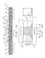
- FIG. 1Ais a cross-sectional view of a flip chip connected to a substrate using the elongated pillars of this invention to illustrate the invention.
- FIG. 1Bis an exploded view of a portion 1 B of the system of FIG. 1A showing in more detail the interconnection between the elongated pillar, the silicon die and the substrate.
- FIGS. 2A-2Gare cross-sectional views of a portion of a semiconductor die and various layers associated with the die to illustrate a process for making the elongated pillars attached to the die and the attachment of such pillars to a substrate to illustrate an embodiment of the invention.
- FIG. 3Ais a perspective view of a flip chip with elongated pillars on one side of the chip to illustrate an embodiment of the invention.
- FIG. 3Bis a cross-sectional view of a portion 3 B of the chip of FIG. 3A to illustrate the embodiment of the invention.
- FIG. 3Cis a cross-sectional view of a portion of the flip chip and the substrate after the flip chip has been attached to the substrate and the underfill material injected to illustrate an embodiment of the invention.
- FIG. 4is a cross-sectional view of a flip chip connected to a substrate where both the flip chip and the substrate are warped to illustrate the shear stress in the chip.
- FIGS. 5A and 5Bare graphical illustrations of shear stress distribution for a 20 mm die where the die is connected to a substrate using elongated pillars of this invention of 100 microns in height and bump diameter of 60 and 100 microns, and at a bump pitch of 100/120/160/225 microns to illustrate the invention.
- FIGS. 6A and 6Bare graphical illustrations of the shear stress in the semiconductor die similar to that shown in FIGS. 5A and 5B except that the height of the elongated pillar is 125 microns instead of 100 microns.
- FIG. 1Ais a cross-sectional view of a semiconductor die in the form of a flip chip 12 connected to a substrate 14 by means of elongated pillars 16 to illustrate an embodiment of the invention.
- the space between the die 12 and substrate 14is filled with an underfill material 18 such as one known to those of skill in the art to provide support and stability to the die and interconnect structure formed by the elongated pillars 16 .
- FIG. 1Bis an exploded view of a portion 1 B of the system of FIG. 1A showing in more detail and elongated pillar connecting a portion of the silicon die to the substrate.
- pillar 16comprises two parts: an upper elongated portion 16 a comprising copper of height H 1 and a second elongated portion of height H 2 comprising a lead-based solder.
- the junction between the two portions 16 a , 16 bis at 16 c .
- the bottom part of portion 16 bis enlarged compared to its upper part and has a substantial conical shape where the bottom part of the solder portion of 16 b is the result of a reflow process as described below to make physical and electrical contact with the copper contact layer 22 on top of substrate 14 .
- portion 16 ais in attached to a copper contact 24 on the silicon die 12 .
- circuits on the silicon die 12are electrically connected through pillar 16 to a copper contact 22 on the substrate 14 .
- the space between the semiconductor die 12 and substrate 14is filled with an underfill material 18 .
- circuits (not shown) on the silicon die 12are spaced apart from the solder portion 16 b by the length or height of portion 16 a containing copper.
- the surface of the silicon die 12 facing the substrateis coated with a passivation layer (not shown) made of a suitable material such as silicon dioxide or polyimide. Therefore, if the length or height H 1 of portion 16 a exceeds the effective thickness shown in the table above, then the circuits on die 12 will not be significantly adversely affected by the ⁇ particle emission from solder 16 b .
- the height H 1 of the portion 16 ais not less than 55 microns, where silicon dioxide is used as the passivation layer, and more preferably, more than 84 microns where polyimide is used as the passivation layer.
- the total height H of pillar 16 between die 12 and the substrate 14is at least 75 microns, such as in the range of about 80-100 microns. For reasons discussed below, a larger value for H would reduce the shear stress experienced by the silicon die and the connection between the die 12 and pillar 16 .
- the total height H of the pillarit may be preferable for the total height H of the pillar to be at least 100 microns, and more preferably 120 microns or more, such as 125 microns. It may be preferable for the ratio H 1 to H 2 to be about 3 to 1.
- FIGS. 2A-2Gare cross-sectional views of a semiconductor die and the various layers associated therewith to illustrate the process for making the elongated pillar interconnect shown in FIGS. 1A, 1 B and of process for connecting the pillar to a substrate to illustrate the invention.
- a photosensitive layer 32is formed on the die 12 .
- FIGS. 2A-2GVarious designated areas of the photosensitive layer are exposed to radiation, and the portions that are exposed to radiation are then removed to yield layer 32 ′ with a pattern of through holes 34 therein as shown in FIG. 2B, where the through holes reach all the way to die 12 .
- Portions of the through holes 34are filled with a material including copper, such as by placing the entire structure in a copper bath. An electric current is passed there through to perform electroplating of the copper material to fill at least a portion of each hole 34 as shown in FIG. 2 C. As shown in FIG.
- the portions 16 b ′ containing solderare then heated in a manner known to those skilled in the art to reflow the solder 16 b ′ to form the solder portions 16 b and pillars 16 as shown in FIGS. 1B and 2G.
- An underfill material 18is then injected to fill the space between die 12 and substrate 14 .
- Contacts 24 on die 12are, therefore, physically and electrically connected and attached to contacts 22 on the substrate 14 .
- the resulting structureis illustrated in FIG. 2 G.
- an underbump metalization layer(typically composed of a material including Titanium (Ti), titanium-tungsten (TiW), or chromuim (Cr)) function as an adhesion layer during the above-described passivation process.
- This layeralso serves as the conducting metal contact for the copper portions of the pillars for the above-described electroplating process.
- the pitch or spacing between adjacent pillarsis in the range of about 80 to about 100 microns. Since solder forms a portion of the pillar, no extra process of placing solder on the substrate is required, and the connection between the pillar and the substrate can be simply formed by reflowing the solder portion of the pillar. Furthermore, through this process, no mushroom solder bump is formed so that finer pitch can be achieved.
- the solder compositionis flexible and can be 63/37 or 5/95 SnPb ratio, or a non-lead solder.
- the copper material and solder material used in the above-described electroplating processesmay simply be copper metal and solder.
- FIG. 4Another advantage of the elongated pillar interconnects of this invention is that it reduces shear stress experienced by warped silicon dies and the connection between the dies and the interconnects. This is illustrated in FIG. 4 .
- the silicon die 12 ′ and substrate 14 ′may become warped for a number of reasons, such as due to thermal effects. Warpage is calculated as Y displacement from center to the corner of the die as shown in FIG. 4 .
- FIGS. 5A and 5Bare graphical plots illustrating shear stress distribution in a die of size 20 mm, where elongated pillars of 100 microns in length and diameters of 60 and 100 microns and at bump pitches of 100, 120, 160, 225 microns.
- pitchis represented as P and diameter is represented by D.
- Ddiameter
- the peak shear stress at the edge of the dieis less than the shear strength of copper so that the elongated pillars of this invention should not fail with the given geometry illustrated, or similar geometries, due to shear stress.
- FIGS. 6A and 6Billustrate similar data to those shown in FIGS. 5A and 5B but where the pillar height or length is 120 microns instead of 100 microns.
- a comparison of FIGS. 6A and 6B to those of FIGS. 5A and 5Bwill illustrate that the longer the pillars, the less will be the shear stress experienced at the edge of the die and the interconnects connected to the die.
- a layer 50 shown in FIG. 1B of either organic or metal materialmay be used to cover the copper portion 16 a .
- Thiswill reduce reliability problems and enables the wetting (due to reduction of surface effects on the otherwise exposed copper surface) of copper sidewall by solder during the above-described reflow process for bonding the pillars to the substrate.
- the material usedmay be Entek or palladium, and may be formed by simply dipping the entire structure (i.e. die 12 and pillar 16 ) into a bath of such material, where the material will only adhere to the copper portion 16 a . Where palladium is used, the layer 50 is formed by electrodeless plating.
Landscapes
- Engineering & Computer Science (AREA)
- Computer Hardware Design (AREA)
- Microelectronics & Electronic Packaging (AREA)
- Power Engineering (AREA)
- Manufacturing & Machinery (AREA)
- Wire Bonding (AREA)
Abstract
Description
This is a division of U.S. patent application Ser. No. 09/564,382, filing date Apr. 27, 2000, now U.S. Pat. No. 6,578,754 Improved Pillar Connections For Semiconductor Chips And Method Of Manufacture, assigned to the same assignee as the present invention.
This invention relates in general to interconnections for semiconductor devices and, in particular, to pillar-shaped connections from a semiconductor chip to a substrate and method for making the connections.
Tin lead based solders is the preferred interconnect material of choice for flip chip bonding of silicon integrated circuits. As dimensions of the electronic devices on the silicon integrated circuits are continually reduced, α particle emissions by lead can cause significant problems. Lead has three stable isotopes which are formed as the end products of natural radioactive decay chains. These stable isotopes, however, usually contain a small amount of residual α particle radioactivity. As the dimensions of electronic devices in silicon integrated circuits become smaller, the distances between the lead-based solder and the devices are also reduced so that the α particle emission from the solder can cause such devices to malfunction.
One way to reduce the effect of α particle emission from solder is to provide a passivation layer covering the electronic devices on silicon. Some materials used for the passivation layer are more effective than others for preserving the integrity of the electronic devices from the α particles. Furthermore, the residual α particle emission from the solder radiate from essentially point sources in the solder, so that the intensity of α particle emission experienced by the electronic devices decreases rapidly with the distances separating the devices from the solder. Shown below is a table setting forth five different materials serving as the medium separating electronic devices from the solder.
| Mol | Effective | |||
| MEDIA | Density | Wt. | −dE/dx | Thickness |
| (Compound) | ρ (g · cm−3) | M(g) | (eV · cm2/1e15 atoms) | d(cm) |
| Air | 1.161e−03 | 39.11 | 20.96 | 10.83 |
| Polyimide | 1.61 | 38.0 | 18.91 | 0.0084 |
| Epoxy | 1.20 | 40.0 | 19.68 | 0.0114 |
| SiO2 | 2.65 | 60.0 | 27.42 | 0.0055 |
| Si3N4 | 3.17 | 140.0 | 28.18 | 0.0105 |
As can be seen from the table above, if air is the only medium that separates the electronic devices from the solder, then in order for the electronic devices not be significantly affected by the α particle emission from the solder, the effective thickness of the air medium separating the electronic devices and the solder should be at least 10.83 cm, which is unacceptable for most applications. From the above table, it will be noted that the best barrier layer substance in terms of minimum absorption length for absorption of α particles from the solder is silicon dioxide, followed by polyimide. Where silicon dioxide or another solid material is used as the passivation layer, only part of the medium separating the electronic devices from the solder is occupied by the material, with the remaining part occupied by air or another material not as effective in absorbing α particles. It will be noted from the table, however, that even where silicon dioxide is used as a compound for the passivation layer covering the electronic devices on silicon, it is preferable that the electronic devices and the solder be separated by at least 0.0055 cm or 55 microns. For polyimide passivation layers, the separation is preferably at least 84 microns. In conventional interconnect systems, lead-based solders are used for connecting flip chips to substrates. Aside from the α particle emission problem described above, as the structural dimensions of electronic devices get smaller, the use of lead-based solder bumps is disadvantageous also because it may be difficult to achieve a fine pitch between adjacent interconnects without bridging which causes electrical shorting. When the solder bump is formed by electroplating, the bump size in the horizontal plane of a 100 micron high solder ball will be around 120 microns, and the solder bump is in the shape of a mushroom. Therefore, if the pitch or distance between adjacent interconnects using solder bumps of such height is reduced to below 150 microns in either the array or peripheral format, bump ridging can easily occur. It is, therefore, desirable to provide an improved interconnect system to achieve finer pitch with minimum probability of bump bridging and where α particle emission will not significantly affect the functions of electronic devices on the semiconductor chips.
In the document entitled “Wire Interconnect Technology, A New High-Reliability Tight-Pitch Interconnect Technology,” by Love et al., from Fujitsu Computer Packaging Technologies, Inc. an all copper interconnect post is proposed. Instead of using lead based solder, the flip chip is connected to a substrate by means of an all copper post which is about 45 or 50 microns in length. While such copper-based interconnects may be able to achieve a finer pitch between adjacent interconnects, such proposed solution still does not avoid the problem of the α particle emission described above. As shown in FIG. 1 of the article by Love et al., solder is used to attach the copper posts to the substrate. Since the height of the copper post or pillars is not more than 50 microns in height, even where silicon dioxide is used as the passivation layer covering the electronic devices on the flip chips, the electronic devices may still be adversely affected by α particle emission by the solder used to attach the copper posts to the substrate. Furthermore, as known to those skilled in the art, the space between the semiconductor flip chip and the substrate is usually filled with an underfill material to provide support and stability to the interconnect structure. Typically, the process of providing the underfill material is by injection that requires a certain minimum separation between the semiconductor chip and the substrate. For most injection processes, the minimum separation is about 75 microns. Therefore, using the interconnect structure proposed by Love et al. in the article, there appears to be inadequate separation between the semiconductor chip and the substrate for injecting the underfill material. The process employed by Love et. al appears to limit the height of the copper post achievable to not more than 50 microns.
None of the above-described interconnect systems is entirely satisfactory. It is, therefore, desirable to provide an improved interconnect system in which the above-described difficulties are not present.
This invention is based on the observation that an elongated pillar may be advantageously used for connecting a semiconductor chip to a substrate, where the pillar comprises two elongated portions, one portion including copper and another portion including solder. The portion including copper is in contact with the semiconductor chip and has a length not less than about 50 microns. Preferably, the total length of the pillar is not less than about 55 microns. In a more preferred embodiment, the length of the pillar is not less than about 85 microns, with the length of the portion of the pillar including copper not less than about 55 microns. Using the elongated pillar of this invention, the separation between the solder in the pillar or any other solder used in the interconnect on the one hand and electronic devices on the semiconductor chip on the other hand can be made to exceed 55 microns or even 84 microns so that the electronic devices on the semiconductor chip will not be adversely effected by α particle emission from the solder when silicon dioxide or polyimide is used as the passivation layer. Where the length of the pillar exceeds 75 microns, adequate separation is provided between the semiconductor chip and the substrate for the injection of the underfill material. Furthermore, by providing elongated pillars of adequate length and suitable cross-sectional dimensions connecting the semiconductor chip to the substrate, the stress induced in the connection between the semiconductor chip and the pillar due to warpage is much reduced, which also reduces the chances of chip failure caused by shear stress on account of the warpage.
The elongated pillar may be formed by first forming a layer of photosensitive material on the chip and exposing to radiation the layer at the predetermined areas. Portions of the layer that are exposed to radiation are removed to form through holes in the layer. Portions of the holes are filled with a material containing copper to form an elongated column of copper material in contact with the chip. Portions of the holes are then filled with a material containing solder to form an elongated column of solder in contact with the copper material, thereby forming a composite pillar, a portion of which includes copper and another portion of which including solder. The photosensitive layer is then removed to form the elongated pillars. After the pillars have been formed, the pillars may be connected to the substrate by placing the pillars in contact with the substrate and heating the solder until the solder reflows. Preferably, the filling of the holes of the photosensitive material layer with copper material or solder is done by electroplating.
FIG. 1A is a cross-sectional view of a flip chip connected to a substrate using the elongated pillars of this invention to illustrate the invention.
FIG. 1B is an exploded view of aportion 1B of the system of FIG. 1A showing in more detail the interconnection between the elongated pillar, the silicon die and the substrate.
FIGS. 2A-2G are cross-sectional views of a portion of a semiconductor die and various layers associated with the die to illustrate a process for making the elongated pillars attached to the die and the attachment of such pillars to a substrate to illustrate an embodiment of the invention.
FIG. 3A is a perspective view of a flip chip with elongated pillars on one side of the chip to illustrate an embodiment of the invention.
FIG. 3B is a cross-sectional view of aportion 3B of the chip of FIG. 3A to illustrate the embodiment of the invention.
FIG. 3C is a cross-sectional view of a portion of the flip chip and the substrate after the flip chip has been attached to the substrate and the underfill material injected to illustrate an embodiment of the invention.
FIG. 4 is a cross-sectional view of a flip chip connected to a substrate where both the flip chip and the substrate are warped to illustrate the shear stress in the chip.
FIGS. 5A and 5B are graphical illustrations of shear stress distribution for a 20 mm die where the die is connected to a substrate using elongated pillars of this invention of 100 microns in height and bump diameter of 60 and 100 microns, and at a bump pitch of 100/120/160/225 microns to illustrate the invention.
FIGS. 6A and 6B are graphical illustrations of the shear stress in the semiconductor die similar to that shown in FIGS. 5A and 5B except that the height of the elongated pillar is 125 microns instead of 100 microns.
For simplicity in description, identical components are identified by the same numerals.
FIG. 1A is a cross-sectional view of a semiconductor die in the form of aflip chip 12 connected to asubstrate 14 by means ofelongated pillars 16 to illustrate an embodiment of the invention. As shown in FIG. 1A, the space between the die12 andsubstrate 14 is filled with anunderfill material 18 such as one known to those of skill in the art to provide support and stability to the die and interconnect structure formed by theelongated pillars 16.
FIG. 1B is an exploded view of aportion 1B of the system of FIG. 1A showing in more detail and elongated pillar connecting a portion of the silicon die to the substrate. As shown in FIG. 1B,pillar 16 comprises two parts: an upperelongated portion 16acomprising copper of height H1 and a second elongated portion of height H2 comprising a lead-based solder. The junction between the twoportions portion 16bis enlarged compared to its upper part and has a substantial conical shape where the bottom part of the solder portion of16bis the result of a reflow process as described below to make physical and electrical contact with thecopper contact layer 22 on top ofsubstrate 14. The upper end ofportion 16ais in attached to acopper contact 24 on the silicon die12. In this manner, circuits on the silicon die12 are electrically connected throughpillar 16 to acopper contact 22 on thesubstrate 14. As shown in FIGS. 1A and 1B, the space between the semiconductor die12 andsubstrate 14 is filled with anunderfill material 18.
As shown in FIG. 1B, circuits (not shown) on the silicon die12 are spaced apart from thesolder portion 16bby the length or height ofportion 16acontaining copper. The surface of the silicon die12 facing the substrate is coated with a passivation layer (not shown) made of a suitable material such as silicon dioxide or polyimide. Therefore, if the length or height H1 ofportion 16aexceeds the effective thickness shown in the table above, then the circuits on die12 will not be significantly adversely affected by the α particle emission fromsolder 16b. In the preferred embodiment, the height H1 of theportion 16ais not less than 55 microns, where silicon dioxide is used as the passivation layer, and more preferably, more than 84 microns where polyimide is used as the passivation layer. To permit many injection processes to be used for injecting theunderfill material 18, the total height H ofpillar 16 betweendie 12 and thesubstrate 14 is at least 75 microns, such as in the range of about 80-100 microns. For reasons discussed below, a larger value for H would reduce the shear stress experienced by the silicon die and the connection between the die12 andpillar 16. Thus, it may be preferable for the total height H of the pillar to be at least 100 microns, and more preferably 120 microns or more, such as 125 microns. It may be preferable for the ratio H1 to H2 to be about 3 to 1.
FIGS. 2A-2G are cross-sectional views of a semiconductor die and the various layers associated therewith to illustrate the process for making the elongated pillar interconnect shown in FIGS. 1A,1B and of process for connecting the pillar to a substrate to illustrate the invention.
As shown in FIG. 2A, aphotosensitive layer 32 is formed on thedie 12. To simplify the drawing, only portions of the die and of the various layers are shown in FIGS. 2A-2G. Various designated areas of the photosensitive layer are exposed to radiation, and the portions that are exposed to radiation are then removed to yieldlayer 32′ with a pattern of throughholes 34 therein as shown in FIG. 2B, where the through holes reach all the way to die12. Portions of the throughholes 34 are filled with a material including copper, such as by placing the entire structure in a copper bath. An electric current is passed there through to perform electroplating of the copper material to fill at least a portion of eachhole 34 as shown in FIG.2C. As shown in FIG. 2C,copper material 16afills a portion of each of holes34. The entire structure is then transferred to a bath of material containing solder and electroplating is again employed to fill portions ofholes 34, resulting in the structure shown in FIG. 2D, where asolder material 16b′ fills portions of theholes 34. The photosensitive remaininglayer 32′ is then removed to form the structure of FIG.2E. As shown in FIG. 2E, twoelongated pillars 16′ are then formed, each comprising acopper portion 16aand asolder portion 16b′. To connect the pillars to the substrate,portions 16b′ are placed in contact with thecopper contacts 22 on thesubstrate 14 as shown in FIG.2F. Theportions 16b′ containing solder are then heated in a manner known to those skilled in the art to reflow thesolder 16b′ to form thesolder portions 16bandpillars 16 as shown in FIGS. 1B and 2G. Anunderfill material 18 is then injected to fill the space betweendie 12 andsubstrate 14.Contacts 24 on die12 are, therefore, physically and electrically connected and attached tocontacts 22 on thesubstrate 14. The resulting structure is illustrated in FIG.2G.
To provide a metal contact between the pillars and the semiconductor die, an underbump metalization layer (typically composed of a material including Titanium (Ti), titanium-tungsten (TiW), or chromuim (Cr)) function as an adhesion layer during the above-described passivation process. This layer also serves as the conducting metal contact for the copper portions of the pillars for the above-described electroplating process. After thephotosensitive layer 32′ has been removed, all portions of this underbump metalization layer, except for the portions underneath the pillars are removed. For simplicity, this layer has been omitted from the figures.
Since the spacing or pitch P between adjacentelongated pillars 16 as illustrated in FIGS. 1A and 2E, fine pitch of not more than 100 microns is achievable preferably, the pitch or spacing between adjacent pillars is in the range of about 80 to about 100 microns. Since solder forms a portion of the pillar, no extra process of placing solder on the substrate is required, and the connection between the pillar and the substrate can be simply formed by reflowing the solder portion of the pillar. Furthermore, through this process, no mushroom solder bump is formed so that finer pitch can be achieved. The solder composition is flexible and can be 63/37 or 5/95 SnPb ratio, or a non-lead solder. The copper material and solder material used in the above-described electroplating processes may simply be copper metal and solder.
Another advantage of the elongated pillar interconnects of this invention is that it reduces shear stress experienced by warped silicon dies and the connection between the dies and the interconnects. This is illustrated in FIG.4. As shown in FIG. 4, the silicon die12′ andsubstrate 14′ may become warped for a number of reasons, such as due to thermal effects. Warpage is calculated as Y displacement from center to the corner of the die as shown in FIG.4. FIGS. 5A and 5B are graphical plots illustrating shear stress distribution in a die ofsize 20 mm, where elongated pillars of 100 microns in length and diameters of 60 and 100 microns and at bump pitches of 100, 120, 160, 225 microns. In the graphical plot, pitch is represented as P and diameter is represented by D. As shown in FIGS. 5A and 5B, the peak shear stress at the edge of the die is less than the shear strength of copper so that the elongated pillars of this invention should not fail with the given geometry illustrated, or similar geometries, due to shear stress. FIGS. 6A and 6B illustrate similar data to those shown in FIGS. 5A and 5B but where the pillar height or length is 120 microns instead of 100 microns. A comparison of FIGS. 6A and 6B to those of FIGS. 5A and 5B will illustrate that the longer the pillars, the less will be the shear stress experienced at the edge of the die and the interconnects connected to the die.
To reduce oxidation of thecopper portion 16a, alayer 50 shown in FIG. 1B of either organic or metal material may be used to cover thecopper portion 16a. This will reduce reliability problems and enables the wetting (due to reduction of surface effects on the otherwise exposed copper surface) of copper sidewall by solder during the above-described reflow process for bonding the pillars to the substrate. The material used may be Entek or palladium, and may be formed by simply dipping the entire structure (i.e. die12 and pillar16) into a bath of such material, where the material will only adhere to thecopper portion 16a. Where palladium is used, thelayer 50 is formed by electrodeless plating.
While the invention has been described above by reference to various embodiments, it will be understood that changes and modifications may be made without departing from the scope of the invention, which is to be defined only by the appended claims and their equivalents.
Claims (6)
1. Method for making electrical connections to a semiconductor chip, comprising:
forming a layer of photosensitive material on the chip;
exposing the layer to radiation at predetermined areas and removing portions of the layer that are exposed to radiation to form through holes in the layer, thereby exposing areas of the chip through the holes;
filling portions of the holes with a copper material to form an elongated column of copper material, so that the copper material is in contact with the chip;
filling portions of the holes with solder to form an elongated column of solder, so that the solder is in contact with the copper material; and
removing the layer.
2. The method ofclaim 1 , wherein the filling is performed by a process that includes electroplating.
3. The method ofclaim 1 , wherein the filling with the copper material is performed so that the elongated column of copper material is not less than about 50 microns in length.
4. The method ofclaim 1 , wherein the filling with the copper material and solder is performed so that the total length of the elongated column of copper material and of the column of solder is not less than about 55 microns in length.
5. The method ofclaim 1 , wherein the filling with the copper material and solder is performed so that the total length of the elongated column of copper material and of the column of solder is not less than about 100 microns in length.
6. The method ofclaim 1 , further comprising placing the column of solder in contact with a substrate and applying heat to the solder to reflow the solder.
Priority Applications (1)
| Application Number | Priority Date | Filing Date | Title |
|---|---|---|---|
| US10/170,089US6681982B2 (en) | 2000-04-27 | 2002-06-12 | Pillar connections for semiconductor chips and method of manufacture |
Applications Claiming Priority (2)
| Application Number | Priority Date | Filing Date | Title |
|---|---|---|---|
| US09/564,382US6578754B1 (en) | 2000-04-27 | 2000-04-27 | Pillar connections for semiconductor chips and method of manufacture |
| US10/170,089US6681982B2 (en) | 2000-04-27 | 2002-06-12 | Pillar connections for semiconductor chips and method of manufacture |
Related Parent Applications (1)
| Application Number | Title | Priority Date | Filing Date |
|---|---|---|---|
| US09/564,382DivisionUS6578754B1 (en) | 2000-04-27 | 2000-04-27 | Pillar connections for semiconductor chips and method of manufacture |
Publications (2)
| Publication Number | Publication Date |
|---|---|
| US20020179689A1 US20020179689A1 (en) | 2002-12-05 |
| US6681982B2true US6681982B2 (en) | 2004-01-27 |
Family
ID=24254234
Family Applications (2)
| Application Number | Title | Priority Date | Filing Date |
|---|---|---|---|
| US09/564,382Expired - LifetimeUS6578754B1 (en) | 2000-04-27 | 2000-04-27 | Pillar connections for semiconductor chips and method of manufacture |
| US10/170,089Expired - LifetimeUS6681982B2 (en) | 2000-04-27 | 2002-06-12 | Pillar connections for semiconductor chips and method of manufacture |
Family Applications Before (1)
| Application Number | Title | Priority Date | Filing Date |
|---|---|---|---|
| US09/564,382Expired - LifetimeUS6578754B1 (en) | 2000-04-27 | 2000-04-27 | Pillar connections for semiconductor chips and method of manufacture |
Country Status (4)
| Country | Link |
|---|---|
| US (2) | US6578754B1 (en) |
| AU (1) | AU2001259194A1 (en) |
| TW (1) | TW510031B (en) |
| WO (1) | WO2001082375A2 (en) |
Cited By (64)
| Publication number | Priority date | Publication date | Assignee | Title |
|---|---|---|---|---|
| US20030127734A1 (en)* | 2002-01-07 | 2003-07-10 | Jin-Yuan Lee | Cylindrical bonding structure and method of manufacture |
| US6884661B1 (en) | 2003-11-04 | 2005-04-26 | Rf Micro Devices, Inc. | Method of fabricating posts over integrated heat sink metallization to enable flip chip packaging of GaAs devices |
| US20050116326A1 (en)* | 2003-10-06 | 2005-06-02 | Tessera, Inc. | Formation of circuitry with modification of feature height |
| US20050173805A1 (en)* | 2003-12-30 | 2005-08-11 | Tessera, Inc. | Micro pin grid array with pin motion isolation |
| US20050181655A1 (en)* | 2003-12-30 | 2005-08-18 | Tessera, Inc. | Micro pin grid array with wiping action |
| US20050284658A1 (en)* | 2003-10-06 | 2005-12-29 | Tessera, Inc. | Components with posts and pads |
| US20060220259A1 (en)* | 2005-01-25 | 2006-10-05 | Ke-Hung Chen | Multi-chip structure and method of assembling chips |
| US7135766B1 (en) | 2004-11-30 | 2006-11-14 | Rf Micro Devices, Inc. | Integrated power devices and signal isolation structure |
| US20070077677A1 (en)* | 2003-12-30 | 2007-04-05 | Tessera, Inc. | Microelectronic packages and methods therefor |
| US20070172690A1 (en)* | 2006-01-24 | 2007-07-26 | Samsung Electronics Co., Ltd. | Joining method, method of mounting semiconductor package using the same, and substrate-joining structure prepared by the joining method |
| US20080088013A1 (en)* | 2006-10-14 | 2008-04-17 | Advanpack Solutons Pte Ltd. | Chip and manufacturing method thereof |
| US20080185686A1 (en)* | 2007-02-05 | 2008-08-07 | Freescale Semiconductor, Inc. | Electronic device with connection bumps |
| US20080227237A1 (en)* | 2002-10-25 | 2008-09-18 | Megica Corporation | Method of assembling chips |
| US20080246163A1 (en)* | 2004-09-28 | 2008-10-09 | Kazumasa Tanida | Semiconductor Device |
| WO2009045371A2 (en) | 2007-09-28 | 2009-04-09 | Tessera, Inc. | Flip chip interconnection with double post |
| US7667473B1 (en)* | 2005-09-28 | 2010-02-23 | Xilinx, Inc | Flip-chip package having thermal expansion posts |
| US20100044860A1 (en)* | 2008-08-21 | 2010-02-25 | Tessera Interconnect Materials, Inc. | Microelectronic substrate or element having conductive pads and metal posts joined thereto using bond layer |
| US7732253B1 (en) | 2006-08-14 | 2010-06-08 | Rf Micro Devices, Inc. | Flip-chip assembly with improved interconnect |
| US20100246150A1 (en)* | 2007-11-06 | 2010-09-30 | Agency For Science Tecnology And Research | Interconnect Structure And A Method Of Fabricating The Same |
| US20110003470A1 (en)* | 2009-07-02 | 2011-01-06 | Flipchip International, Llc | Methods and structures for a vertical pillar interconnect |
| US20110084386A1 (en)* | 2003-11-10 | 2011-04-14 | Stats Chippac, Ltd. | Semiconductor Device and Method of Self-Confinement of Conductive Bump Material During Reflow Without Solder Mask |
| US20110084381A1 (en)* | 2009-10-14 | 2011-04-14 | Jian-Wen Lo | Chip Having A Metal Pillar Structure |
| US20110121464A1 (en)* | 2009-11-24 | 2011-05-26 | Stats Chippac, Ltd. | Semiconductor Device and Method of Forming Electrical Interconnect with Stress Relief Void |
| US20110233763A1 (en)* | 2010-03-26 | 2011-09-29 | Pendse Rajendra D | Integrated circuit system with stress redistribution layer and method of manufacture thereof |
| WO2012006403A1 (en) | 2010-07-08 | 2012-01-12 | Tessera, Inc. | Microelectronic package with dual or multiple - etched flip -chip connectors and corresponding manufacturing method |
| US8232193B2 (en) | 2010-07-08 | 2012-07-31 | Taiwan Semiconductor Manufacturing Company, Ltd. | Method of forming Cu pillar capped by barrier layer |
| WO2012145114A1 (en) | 2011-04-21 | 2012-10-26 | Tessera, Inc. | Flip-chip, face-up and face-down wirebond combination package |
| US20120280755A1 (en)* | 2011-05-04 | 2012-11-08 | Triquint Semiconductor, Inc. | Flip-chip power amplifier and impedance matching network |
| US8367467B2 (en) | 2010-04-21 | 2013-02-05 | Stats Chippac, Ltd. | Semiconductor method of forming bump on substrate to prevent ELK ILD delamination during reflow process |
| US20130127045A1 (en)* | 2011-11-22 | 2013-05-23 | Taiwan Semiconductor Manufacturing Company, Ltd. | Mechanisms for forming fine-pitch copper bump structures |
| WO2013086106A1 (en) | 2011-12-09 | 2013-06-13 | Robert Bosch Gmbh | Mems chip scale package |
| US8492893B1 (en) | 2011-03-16 | 2013-07-23 | Amkor Technology, Inc. | Semiconductor device capable of preventing dielectric layer from cracking |
| US8492891B2 (en) | 2010-04-22 | 2013-07-23 | Taiwan Semiconductor Manufacturing Company, Ltd. | Cu pillar bump with electrolytic metal sidewall protection |
| US8496159B2 (en) | 2011-06-06 | 2013-07-30 | International Business Machines Corporation | Injection molded solder process for forming solder bumps on substrates |
| US8536458B1 (en) | 2009-03-30 | 2013-09-17 | Amkor Technology, Inc. | Fine pitch copper pillar package and method |
| US8552553B2 (en) | 2009-10-14 | 2013-10-08 | Advanced Semiconductor Engineering, Inc. | Semiconductor device |
| US8569885B2 (en) | 2010-10-29 | 2013-10-29 | Advanced Semiconductor Engineering, Inc. | Stacked semiconductor packages and related methods |
| US8580607B2 (en) | 2010-07-27 | 2013-11-12 | Tessera, Inc. | Microelectronic packages with nanoparticle joining |
| US20130341786A1 (en)* | 2012-06-25 | 2013-12-26 | Taiwan Semiconductor Manufacturing Company, Ltd. | Package on Package Devices and Methods of Packaging Semiconductor Dies |
| US8641913B2 (en) | 2003-10-06 | 2014-02-04 | Tessera, Inc. | Fine pitch microcontacts and method for forming thereof |
| US8686568B2 (en) | 2012-09-27 | 2014-04-01 | Advanced Semiconductor Engineering, Inc. | Semiconductor package substrates having layered circuit segments, and related methods |
| US8698307B2 (en) | 2010-09-27 | 2014-04-15 | Advanced Semiconductor Engineering, Inc. | Semiconductor package with integrated metal pillars and manufacturing methods thereof |
| US8716790B2 (en) | 2004-01-29 | 2014-05-06 | Enpirion, Inc. | Laterally diffused metal oxide semiconductor device and method of forming the same |
| EP2738807A2 (en) | 2012-11-30 | 2014-06-04 | Enpirion, Inc. | An apparatus including a semiconductor device coupled to a decoupling device |
| US8803333B2 (en) | 2012-05-18 | 2014-08-12 | Taiwan Semiconductor Manufacturing Company, Ltd. | Three-dimensional chip stack and method of forming the same |
| US8810029B2 (en) | 2003-11-10 | 2014-08-19 | Stats Chippac, Ltd. | Solder joint flip chip interconnection |
| US8841779B2 (en) | 2005-03-25 | 2014-09-23 | Stats Chippac, Ltd. | Semiconductor device and method of forming high routing density BOL BONL and BONP interconnect sites on substrate |
| US8853558B2 (en) | 2010-12-10 | 2014-10-07 | Tessera, Inc. | Interconnect structure |
| US8884443B2 (en) | 2012-07-05 | 2014-11-11 | Advanced Semiconductor Engineering, Inc. | Substrate for semiconductor package and process for manufacturing |
| US9064858B2 (en) | 2003-11-10 | 2015-06-23 | Stats Chippac, Ltd. | Semiconductor device and method of forming bump-on-lead interconnection |
| US9159665B2 (en) | 2005-03-25 | 2015-10-13 | Stats Chippac, Ltd. | Flip chip interconnection having narrow interconnection sites on the substrate |
| US9219045B2 (en) | 2003-11-10 | 2015-12-22 | Stats Chippac, Ltd. | Semiconductor device and method of self-confinement of conductive bump material during reflow without solder mask |
| US9252094B2 (en) | 2011-04-30 | 2016-02-02 | Stats Chippac, Ltd. | Semiconductor device and method of forming an interconnect structure with conductive material recessed within conductive ring over surface of conductive pillar |
| US9627254B2 (en) | 2009-07-02 | 2017-04-18 | Flipchip International, Llc | Method for building vertical pillar interconnect |
| US9633971B2 (en) | 2015-07-10 | 2017-04-25 | Invensas Corporation | Structures and methods for low temperature bonding using nanoparticles |
| US9773685B2 (en) | 2003-11-10 | 2017-09-26 | STATS ChipPAC Pte. Ltd. | Solder joint flip chip interconnection having relief structure |
| US9793877B2 (en) | 2013-12-17 | 2017-10-17 | Avago Technologies General Ip (Singapore) Pte. Ltd. | Encapsulated bulk acoustic wave (BAW) resonator device |
| US9922915B2 (en) | 2003-11-10 | 2018-03-20 | STATS ChipPAC Pte. Ltd. | Bump-on-lead flip chip interconnection |
| USRE47600E1 (en) | 2003-11-10 | 2019-09-10 | STATS ChipPAC Pte. Ltd. | Semiconductor device and method of forming electrical interconnect with stress relief void |
| US10535626B2 (en) | 2015-07-10 | 2020-01-14 | Invensas Corporation | Structures and methods for low temperature bonding using nanoparticles |
| US10777524B2 (en) | 2012-07-23 | 2020-09-15 | Qorvo Us, Inc. | Using an interconnect bump to traverse through a passivation layer of a semiconductor die |
| US11842972B2 (en) | 2004-09-28 | 2023-12-12 | Rohm Co., Ltd. | Semiconductor device with a semiconductor chip connected in a flip chip manner |
| US11973056B2 (en) | 2016-10-27 | 2024-04-30 | Adeia Semiconductor Technologies Llc | Methods for low temperature bonding using nanoparticles |
| US12211809B2 (en) | 2020-12-30 | 2025-01-28 | Adeia Semiconductor Bonding Technologies Inc. | Structure with conductive feature and method of forming same |
Families Citing this family (169)
| Publication number | Priority date | Publication date | Assignee | Title |
|---|---|---|---|---|
| US6826827B1 (en)* | 1994-12-29 | 2004-12-07 | Tessera, Inc. | Forming conductive posts by selective removal of conductive material |
| US6642136B1 (en)* | 2001-09-17 | 2003-11-04 | Megic Corporation | Method of making a low fabrication cost, high performance, high reliability chip scale package |
| US7381642B2 (en)* | 2004-09-23 | 2008-06-03 | Megica Corporation | Top layers of metal for integrated circuits |
| US6303423B1 (en)* | 1998-12-21 | 2001-10-16 | Megic Corporation | Method for forming high performance system-on-chip using post passivation process |
| US6965165B2 (en) | 1998-12-21 | 2005-11-15 | Mou-Shiung Lin | Top layers of metal for high performance IC's |
| US7416971B2 (en)* | 2004-09-23 | 2008-08-26 | Megica Corporation | Top layers of metal for integrated circuits |
| US7405149B1 (en)* | 1998-12-21 | 2008-07-29 | Megica Corporation | Post passivation method for semiconductor chip or wafer |
| US8021976B2 (en)* | 2002-10-15 | 2011-09-20 | Megica Corporation | Method of wire bonding over active area of a semiconductor circuit |
| US6495442B1 (en)* | 2000-10-18 | 2002-12-17 | Magic Corporation | Post passivation interconnection schemes on top of the IC chips |
| US6936531B2 (en)* | 1998-12-21 | 2005-08-30 | Megic Corporation | Process of fabricating a chip structure |
| US6520402B2 (en)* | 2000-05-22 | 2003-02-18 | The Regents Of The University Of California | High-speed direct writing with metallic microspheres |
| US7271489B2 (en)* | 2003-10-15 | 2007-09-18 | Megica Corporation | Post passivation interconnection schemes on top of the IC chips |
| US6884313B2 (en)* | 2001-01-08 | 2005-04-26 | Fujitsu Limited | Method and system for joining and an ultra-high density interconnect |
| US6800169B2 (en)* | 2001-01-08 | 2004-10-05 | Fujitsu Limited | Method for joining conductive structures and an electrical conductive article |
| US6815324B2 (en)* | 2001-02-15 | 2004-11-09 | Megic Corporation | Reliable metal bumps on top of I/O pads after removal of test probe marks |
| US6818545B2 (en) | 2001-03-05 | 2004-11-16 | Megic Corporation | Low fabrication cost, fine pitch and high reliability solder bump |
| US7902679B2 (en)* | 2001-03-05 | 2011-03-08 | Megica Corporation | Structure and manufacturing method of a chip scale package with low fabrication cost, fine pitch and high reliability solder bump |
| US6869515B2 (en) | 2001-03-30 | 2005-03-22 | Uri Cohen | Enhanced electrochemical deposition (ECD) filling of high aspect ratio openings |
| US6732913B2 (en)* | 2001-04-26 | 2004-05-11 | Advanpack Solutions Pte Ltd. | Method for forming a wafer level chip scale package, and package formed thereby |
| US7099293B2 (en)* | 2002-05-01 | 2006-08-29 | Stmicroelectronics, Inc. | Buffer-less de-skewing for symbol combination in a CDMA demodulator |
| JP4015490B2 (en)* | 2001-09-26 | 2007-11-28 | 株式会社ルネサステクノロジ | Manufacturing method of semiconductor device |
| US6798073B2 (en)* | 2001-12-13 | 2004-09-28 | Megic Corporation | Chip structure and process for forming the same |
| US7932603B2 (en)* | 2001-12-13 | 2011-04-26 | Megica Corporation | Chip structure and process for forming the same |
| US6661102B1 (en)* | 2002-01-18 | 2003-12-09 | Advance Micro Devices, Inc. | Semiconductor packaging apparatus for controlling die attach fillet height to reduce die shear stress |
| US20040007779A1 (en)* | 2002-07-15 | 2004-01-15 | Diane Arbuthnot | Wafer-level method for fine-pitch, high aspect ratio chip interconnect |
| US6802945B2 (en)* | 2003-01-06 | 2004-10-12 | Megic Corporation | Method of metal sputtering for integrated circuit metal routing |
| US7423340B2 (en)* | 2003-01-21 | 2008-09-09 | Siliconware Precision Industries Co., Ltd. | Semiconductor package free of substrate and fabrication method thereof |
| TWI241000B (en)* | 2003-01-21 | 2005-10-01 | Siliconware Precision Industries Co Ltd | Semiconductor package and fabricating method thereof |
| US7342318B2 (en)* | 2003-01-21 | 2008-03-11 | Siliconware Precision Industries Co., Ltd. | Semiconductor package free of substrate and fabrication method thereof |
| US7271493B2 (en)* | 2003-01-21 | 2007-09-18 | Siliconware Precision Industries Co., Ltd. | Semiconductor package free of substrate and fabrication method thereof |
| US20050184368A1 (en)* | 2003-01-21 | 2005-08-25 | Huang Chien P. | Semiconductor package free of substrate and fabrication method thereof |
| US20050194665A1 (en)* | 2003-01-21 | 2005-09-08 | Huang Chien P. | Semiconductor package free of substrate and fabrication method thereof |
| US20040222518A1 (en)* | 2003-02-25 | 2004-11-11 | Tessera, Inc. | Ball grid array with bumps |
| US20050026416A1 (en)* | 2003-07-31 | 2005-02-03 | International Business Machines Corporation | Encapsulated pin structure for improved reliability of wafer |
| US7462942B2 (en)* | 2003-10-09 | 2008-12-09 | Advanpack Solutions Pte Ltd | Die pillar structures and a method of their formation |
| US7394161B2 (en)* | 2003-12-08 | 2008-07-01 | Megica Corporation | Chip structure with pads having bumps or wirebonded wires formed thereover or used to be tested thereto |
| US20050168231A1 (en)* | 2003-12-24 | 2005-08-04 | Young-Gon Kim | Methods and structures for electronic probing arrays |
| WO2005093816A1 (en)* | 2004-03-05 | 2005-10-06 | Infineon Technologies Ag | Semiconductor device for radio frequency applications and method for making the same |
| US7453157B2 (en)* | 2004-06-25 | 2008-11-18 | Tessera, Inc. | Microelectronic packages and methods therefor |
| US8022544B2 (en) | 2004-07-09 | 2011-09-20 | Megica Corporation | Chip structure |
| US7465654B2 (en)* | 2004-07-09 | 2008-12-16 | Megica Corporation | Structure of gold bumps and gold conductors on one IC die and methods of manufacturing the structures |
| US8067837B2 (en) | 2004-09-20 | 2011-11-29 | Megica Corporation | Metallization structure over passivation layer for IC chip |
| US8008775B2 (en) | 2004-09-09 | 2011-08-30 | Megica Corporation | Post passivation interconnection structures |
| US7423346B2 (en)* | 2004-09-09 | 2008-09-09 | Megica Corporation | Post passivation interconnection process and structures |
| US7355282B2 (en)* | 2004-09-09 | 2008-04-08 | Megica Corporation | Post passivation interconnection process and structures |
| US7521805B2 (en)* | 2004-10-12 | 2009-04-21 | Megica Corp. | Post passivation interconnection schemes on top of the IC chips |
| KR101313391B1 (en) | 2004-11-03 | 2013-10-01 | 테세라, 인코포레이티드 | Stacked packaging improvements |
| US7523852B2 (en)* | 2004-12-05 | 2009-04-28 | International Business Machines Corporation | Solder interconnect structure and method using injection molded solder |
| US7323406B2 (en)* | 2005-01-27 | 2008-01-29 | Chartered Semiconductor Manufacturing Ltd. | Elevated bond-pad structure for high-density flip-clip packaging and a method of fabricating the structures |
| US7939934B2 (en)* | 2005-03-16 | 2011-05-10 | Tessera, Inc. | Microelectronic packages and methods therefor |
| US8384189B2 (en)* | 2005-03-29 | 2013-02-26 | Megica Corporation | High performance system-on-chip using post passivation process |
| US20060223313A1 (en)* | 2005-04-01 | 2006-10-05 | Agency For Science, Technology And Research | Copper interconnect post for connecting a semiconductor chip to a substrate and method of fabricating the same |
| US7687925B2 (en) | 2005-09-07 | 2010-03-30 | Infineon Technologies Ag | Alignment marks for polarized light lithography and method for use thereof |
| DE112006002428A5 (en)* | 2005-09-14 | 2008-12-11 | Htc Beteiligungs Gmbh | Flip-chip module and method for generating a flip-chip module |
| US7630210B2 (en)* | 2005-11-29 | 2009-12-08 | Amphenol Corporation | Lead(Pb)-free electronic component attachment |
| US8058101B2 (en) | 2005-12-23 | 2011-11-15 | Tessera, Inc. | Microelectronic packages and methods therefor |
| US8067267B2 (en)* | 2005-12-23 | 2011-11-29 | Tessera, Inc. | Microelectronic assemblies having very fine pitch stacking |
| DE102006006561B4 (en)* | 2006-02-13 | 2009-03-05 | Htc Beteiligungs Gmbh | Flip-chip module and method for exchanging a semiconductor chip of a flip-chip module |
| US7494924B2 (en)* | 2006-03-06 | 2009-02-24 | Freescale Semiconductor, Inc. | Method for forming reinforced interconnects on a substrate |
| US7545029B2 (en)* | 2006-08-18 | 2009-06-09 | Tessera, Inc. | Stack microelectronic assemblies |
| TWI370515B (en)* | 2006-09-29 | 2012-08-11 | Megica Corp | Circuit component |
| US7510401B2 (en)* | 2006-10-12 | 2009-03-31 | Tessera, Inc. | Microelectronic component with foam-metal posts |
| US7719121B2 (en)* | 2006-10-17 | 2010-05-18 | Tessera, Inc. | Microelectronic packages and methods therefor |
| US20080150101A1 (en)* | 2006-12-20 | 2008-06-26 | Tessera, Inc. | Microelectronic packages having improved input/output connections and methods therefor |
| TWI343084B (en)* | 2006-12-28 | 2011-06-01 | Siliconware Precision Industries Co Ltd | Semiconductor device having conductive bumps and fabrication methodthereof |
| US20090014852A1 (en)* | 2007-07-11 | 2009-01-15 | Hsin-Hui Lee | Flip-Chip Packaging with Stud Bumps |
| US20090108443A1 (en)* | 2007-10-30 | 2009-04-30 | Monolithic Power Systems, Inc. | Flip-Chip Interconnect Structure |
| DE102009012643A1 (en) | 2008-03-10 | 2009-10-01 | Fraunhofer-Gesellschaft zur Förderung der angewandten Forschung e.V. | Connecting structure for connecting electronic component i.e. semiconductor chip, and/or substrate carrier on organic printed circuit board, has contact elements at which material of component or carrier is removed for forming free area |
| US9524945B2 (en) | 2010-05-18 | 2016-12-20 | Taiwan Semiconductor Manufacturing Company, Ltd. | Cu pillar bump with L-shaped non-metal sidewall protection structure |
| US7569935B1 (en)* | 2008-11-12 | 2009-08-04 | Powertech Technology Inc. | Pillar-to-pillar flip-chip assembly |
| US9035459B2 (en) | 2009-04-10 | 2015-05-19 | International Business Machines Corporation | Structures for improving current carrying capability of interconnects and methods of fabricating the same |
| US8841766B2 (en) | 2009-07-30 | 2014-09-23 | Taiwan Semiconductor Manufacturing Company, Ltd. | Cu pillar bump with non-metal sidewall protection structure |
| US8377816B2 (en)* | 2009-07-30 | 2013-02-19 | Taiwan Semiconductor Manufacturing Company, Ltd. | Method of forming electrical connections |
| US8324738B2 (en)* | 2009-09-01 | 2012-12-04 | Taiwan Semiconductor Manufacturing Company, Ltd. | Self-aligned protection layer for copper post structure |
| US8569897B2 (en)* | 2009-09-14 | 2013-10-29 | Taiwan Semiconductor Manufacturing Company, Ltd. | Protection layer for preventing UBM layer from chemical attack and oxidation |
| US8609526B2 (en)* | 2009-10-20 | 2013-12-17 | Taiwan Semiconductor Manufacturing Company, Ltd. | Preventing UBM oxidation in bump formation processes |
| US9024431B2 (en)* | 2009-10-29 | 2015-05-05 | Taiwan Semiconductor Manufacturing Company, Ltd. | Semiconductor die contact structure and method |
| US9607936B2 (en)* | 2009-10-29 | 2017-03-28 | Taiwan Semiconductor Manufacturing Company, Ltd. | Copper bump joint structures with improved crack resistance |
| US8847387B2 (en)* | 2009-10-29 | 2014-09-30 | Taiwan Semiconductor Manufacturing Company, Ltd. | Robust joint structure for flip-chip bonding |
| US8659155B2 (en) | 2009-11-05 | 2014-02-25 | Taiwan Semiconductor Manufacturing Company, Ltd. | Mechanisms for forming copper pillar bumps |
| US8569887B2 (en)* | 2009-11-05 | 2013-10-29 | Taiwan Semiconductor Manufacturing Company, Ltd. | Post passivation interconnect with oxidation prevention layer |
| US8610270B2 (en) | 2010-02-09 | 2013-12-17 | Taiwan Semiconductor Manufacturing Company, Ltd. | Semiconductor device and semiconductor assembly with lead-free solder |
| US8193639B2 (en) | 2010-03-30 | 2012-06-05 | Taiwan Semiconductor Manufacturing Company, Ltd. | Dummy metal design for packaging structures |
| US8441124B2 (en) | 2010-04-29 | 2013-05-14 | Taiwan Semiconductor Manufacturing Company, Ltd. | Cu pillar bump with non-metal sidewall protection structure |
| US9142533B2 (en)* | 2010-05-20 | 2015-09-22 | Taiwan Semiconductor Manufacturing Company, Ltd. | Substrate interconnections having different sizes |
| US9018758B2 (en) | 2010-06-02 | 2015-04-28 | Taiwan Semiconductor Manufacturing Company, Ltd. | Cu pillar bump with non-metal sidewall spacer and metal top cap |
| US8922004B2 (en) | 2010-06-11 | 2014-12-30 | Taiwan Semiconductor Manufacturing Company, Ltd. | Copper bump structures having sidewall protection layers |
| US20120009777A1 (en) | 2010-07-07 | 2012-01-12 | Taiwan Semiconductor Manufacturing Company, Ltd. | UBM Etching Methods |
| US9159708B2 (en) | 2010-07-19 | 2015-10-13 | Tessera, Inc. | Stackable molded microelectronic packages with area array unit connectors |
| US8482111B2 (en) | 2010-07-19 | 2013-07-09 | Tessera, Inc. | Stackable molded microelectronic packages |
| US8546254B2 (en) | 2010-08-19 | 2013-10-01 | Taiwan Semiconductor Manufacturing Company, Ltd. | Mechanisms for forming copper pillar bumps using patterned anodes |
| KR101075241B1 (en) | 2010-11-15 | 2011-11-01 | 테세라, 인코포레이티드 | Microelectronic package with terminals in dielectric member |
| US8492892B2 (en) | 2010-12-08 | 2013-07-23 | International Business Machines Corporation | Solder bump connections |
| US20120146206A1 (en) | 2010-12-13 | 2012-06-14 | Tessera Research Llc | Pin attachment |
| US9137903B2 (en) | 2010-12-21 | 2015-09-15 | Tessera, Inc. | Semiconductor chip assembly and method for making same |
| US9093332B2 (en) | 2011-02-08 | 2015-07-28 | Taiwan Semiconductor Manufacturing Company, Ltd. | Elongated bump structure for semiconductor devices |
| US8618659B2 (en) | 2011-05-03 | 2013-12-31 | Tessera, Inc. | Package-on-package assembly with wire bonds to encapsulation surface |
| KR101128063B1 (en) | 2011-05-03 | 2012-04-23 | 테세라, 인코포레이티드 | Package-on-package assembly with wire bonds to encapsulation surface |
| US8610285B2 (en) | 2011-05-30 | 2013-12-17 | Taiwan Semiconductor Manufacturing Company, Ltd. | 3D IC packaging structures and methods with a metal pillar |
| US8664760B2 (en) | 2011-05-30 | 2014-03-04 | Taiwan Semiconductor Manufacturing Company, Ltd. | Connector design for packaging integrated circuits |
| US8508054B2 (en)* | 2011-06-16 | 2013-08-13 | Broadcom Corporation | Enhanced bump pitch scaling |
| US8716858B2 (en) | 2011-06-24 | 2014-05-06 | Taiwan Semiconductor Manufacturing Company, Ltd. | Bump structure with barrier layer on post-passivation interconnect |
| US8872318B2 (en) | 2011-08-24 | 2014-10-28 | Tessera, Inc. | Through interposer wire bond using low CTE interposer with coarse slot apertures |
| US8598691B2 (en)* | 2011-09-09 | 2013-12-03 | Taiwan Semiconductor Manufacturing Company, Ltd. | Semiconductor devices and methods of manufacturing and packaging thereof |
| US8581400B2 (en) | 2011-10-13 | 2013-11-12 | Taiwan Semiconductor Manufacturing Company, Ltd. | Post-passivation interconnect structure |
| US8836136B2 (en) | 2011-10-17 | 2014-09-16 | Invensas Corporation | Package-on-package assembly with wire bond vias |
| US9824923B2 (en) | 2011-10-17 | 2017-11-21 | STATS ChipPAC Pte. Ltd. | Semiconductor device and method of forming conductive pillar having an expanded base |
| US9786622B2 (en)* | 2011-10-20 | 2017-10-10 | Taiwan Semiconductor Manufacturing Company, Ltd. | Semiconductor package |
| US9385076B2 (en) | 2011-12-07 | 2016-07-05 | Taiwan Semiconductor Manufacturing Company, Ltd. | Semiconductor device with bump structure on an interconncet structure |
| US9613914B2 (en) | 2011-12-07 | 2017-04-04 | Taiwan Semiconductor Manufacturing Company, Ltd. | Post-passivation interconnect structure |
| US8946757B2 (en) | 2012-02-17 | 2015-02-03 | Invensas Corporation | Heat spreading substrate with embedded interconnects |
| US9349706B2 (en) | 2012-02-24 | 2016-05-24 | Invensas Corporation | Method for package-on-package assembly with wire bonds to encapsulation surface |
| US8372741B1 (en) | 2012-02-24 | 2013-02-12 | Invensas Corporation | Method for package-on-package assembly with wire bonds to encapsulation surface |
| US9646923B2 (en) | 2012-04-17 | 2017-05-09 | Taiwan Semiconductor Manufacturing Company, Ltd. | Semiconductor devices, methods of manufacture thereof, and packaged semiconductor devices |
| US9425136B2 (en) | 2012-04-17 | 2016-08-23 | Taiwan Semiconductor Manufacturing Company, Ltd. | Conical-shaped or tier-shaped pillar connections |
| US9299674B2 (en) | 2012-04-18 | 2016-03-29 | Taiwan Semiconductor Manufacturing Company, Ltd. | Bump-on-trace interconnect |
| US8835228B2 (en) | 2012-05-22 | 2014-09-16 | Invensas Corporation | Substrate-less stackable package with wire-bond interconnect |
| US9472521B2 (en) | 2012-05-30 | 2016-10-18 | Taiwan Semiconductor Manufacturing Company, Ltd. | Scheme for connector site spacing and resulting structures |
| US9190348B2 (en) | 2012-05-30 | 2015-11-17 | Taiwan Semiconductor Manufacturing Company, Ltd. | Scheme for connector site spacing and resulting structures |
| US9391008B2 (en) | 2012-07-31 | 2016-07-12 | Invensas Corporation | Reconstituted wafer-level package DRAM |
| US9502390B2 (en) | 2012-08-03 | 2016-11-22 | Invensas Corporation | BVA interposer |
| US9111817B2 (en) | 2012-09-18 | 2015-08-18 | Taiwan Semiconductor Manufacturing Company, Ltd. | Bump structure and method of forming same |
| US8866311B2 (en) | 2012-09-21 | 2014-10-21 | Advanced Semiconductor Engineering, Inc. | Semiconductor package substrates having pillars and related methods |
| US8975738B2 (en) | 2012-11-12 | 2015-03-10 | Invensas Corporation | Structure for microelectronic packaging with terminals on dielectric mass |
| JP6143104B2 (en) | 2012-12-05 | 2017-06-07 | 株式会社村田製作所 | Bumped electronic component and method for manufacturing bumped electronic component |
| US8878353B2 (en) | 2012-12-20 | 2014-11-04 | Invensas Corporation | Structure for microelectronic packaging with bond elements to encapsulation surface |
| US9136254B2 (en) | 2013-02-01 | 2015-09-15 | Invensas Corporation | Microelectronic package having wire bond vias and stiffening layer |
| US9034696B2 (en) | 2013-07-15 | 2015-05-19 | Invensas Corporation | Microelectronic assemblies having reinforcing collars on connectors extending through encapsulation |
| US9023691B2 (en) | 2013-07-15 | 2015-05-05 | Invensas Corporation | Microelectronic assemblies with stack terminals coupled by connectors extending through encapsulation |
| US8883563B1 (en) | 2013-07-15 | 2014-11-11 | Invensas Corporation | Fabrication of microelectronic assemblies having stack terminals coupled by connectors extending through encapsulation |
| US9167710B2 (en) | 2013-08-07 | 2015-10-20 | Invensas Corporation | Embedded packaging with preformed vias |
| US9685365B2 (en) | 2013-08-08 | 2017-06-20 | Invensas Corporation | Method of forming a wire bond having a free end |
| US20150076714A1 (en) | 2013-09-16 | 2015-03-19 | Invensas Corporation | Microelectronic element with bond elements to encapsulation surface |
| US20150122661A1 (en)* | 2013-11-05 | 2015-05-07 | Rohm And Haas Electronic Materials Llc | Plating bath and method |
| US9082753B2 (en) | 2013-11-12 | 2015-07-14 | Invensas Corporation | Severing bond wire by kinking and twisting |
| US9087815B2 (en) | 2013-11-12 | 2015-07-21 | Invensas Corporation | Off substrate kinking of bond wire |
| US9379074B2 (en) | 2013-11-22 | 2016-06-28 | Invensas Corporation | Die stacks with one or more bond via arrays of wire bond wires and with one or more arrays of bump interconnects |
| US9583456B2 (en) | 2013-11-22 | 2017-02-28 | Invensas Corporation | Multiple bond via arrays of different wire heights on a same substrate |
| US9263394B2 (en) | 2013-11-22 | 2016-02-16 | Invensas Corporation | Multiple bond via arrays of different wire heights on a same substrate |
| US9583411B2 (en) | 2014-01-17 | 2017-02-28 | Invensas Corporation | Fine pitch BVA using reconstituted wafer with area array accessible for testing |
| US9214454B2 (en) | 2014-03-31 | 2015-12-15 | Invensas Corporation | Batch process fabrication of package-on-package microelectronic assemblies |
| CN103887276B (en)* | 2014-04-04 | 2016-06-01 | 华进半导体封装先导技术研发中心有限公司 | Prevent bump structure and the forming method of convex some side direction etching |
| US10381326B2 (en) | 2014-05-28 | 2019-08-13 | Invensas Corporation | Structure and method for integrated circuits packaging with increased density |
| US9646917B2 (en) | 2014-05-29 | 2017-05-09 | Invensas Corporation | Low CTE component with wire bond interconnects |
| US9412714B2 (en) | 2014-05-30 | 2016-08-09 | Invensas Corporation | Wire bond support structure and microelectronic package including wire bonds therefrom |
| TWI661494B (en) | 2014-07-31 | 2019-06-01 | 美商西凱渥資訊處理科技公司 | Multilayered transient liquid phase bonding |
| US10541152B2 (en) | 2014-07-31 | 2020-01-21 | Skyworks Solutions, Inc. | Transient liquid phase material bonding and sealing structures and methods of forming same |
| US9735084B2 (en) | 2014-12-11 | 2017-08-15 | Invensas Corporation | Bond via array for thermal conductivity |
| US9888579B2 (en) | 2015-03-05 | 2018-02-06 | Invensas Corporation | Pressing of wire bond wire tips to provide bent-over tips |
| US9502372B1 (en) | 2015-04-30 | 2016-11-22 | Invensas Corporation | Wafer-level packaging using wire bond wires in place of a redistribution layer |
| US9761554B2 (en) | 2015-05-07 | 2017-09-12 | Invensas Corporation | Ball bonding metal wire bond wires to metal pads |
| US9932684B2 (en) | 2015-08-06 | 2018-04-03 | Rohm And Haas Electronic Materials Llc | Method of electroplating photoresist defined features from copper electroplating baths containing reaction products of alpha amino acids and bisepoxides |
| TWI608132B (en) | 2015-08-06 | 2017-12-11 | 羅門哈斯電子材料有限公司 | Method of electroplating photoresist defined features from copper electroplating baths containing reaction products of pyridyl alkylamines and bisepoxides |
| US10100421B2 (en) | 2015-08-06 | 2018-10-16 | Dow Global Technologies Llc | Method of electroplating photoresist defined features from copper electroplating baths containing reaction products of imidazole and bisepoxide compounds |
| US10006136B2 (en) | 2015-08-06 | 2018-06-26 | Dow Global Technologies Llc | Method of electroplating photoresist defined features from copper electroplating baths containing reaction products of imidazole compounds, bisepoxides and halobenzyl compounds |
| DE112015006855T5 (en)* | 2015-08-28 | 2018-08-16 | Intel IP Corporation | Microelectronic packages with highly integrated microelectronics dice stack |
| US9754911B2 (en) | 2015-10-05 | 2017-09-05 | Globalfoundries Inc. | IC structure with angled interconnect elements |
| US9490222B1 (en) | 2015-10-12 | 2016-11-08 | Invensas Corporation | Wire bond wires for interference shielding |
| US10490528B2 (en) | 2015-10-12 | 2019-11-26 | Invensas Corporation | Embedded wire bond wires |
| US10332854B2 (en) | 2015-10-23 | 2019-06-25 | Invensas Corporation | Anchoring structure of fine pitch bva |
| US10181457B2 (en) | 2015-10-26 | 2019-01-15 | Invensas Corporation | Microelectronic package for wafer-level chip scale packaging with fan-out |
| US10043779B2 (en) | 2015-11-17 | 2018-08-07 | Invensas Corporation | Packaged microelectronic device for a package-on-package device |
| US9659848B1 (en) | 2015-11-18 | 2017-05-23 | Invensas Corporation | Stiffened wires for offset BVA |
| US9984992B2 (en) | 2015-12-30 | 2018-05-29 | Invensas Corporation | Embedded wire bond wires for vertical integration with separate surface mount and wire bond mounting surfaces |
| US10325828B2 (en)* | 2016-03-30 | 2019-06-18 | Qorvo Us, Inc. | Electronics package with improved thermal performance |
| US10643965B2 (en)* | 2016-05-25 | 2020-05-05 | Taiwan Semiconductor Manufacturing Company, Ltd. | Structure and method of forming a joint assembly |
| US9935075B2 (en) | 2016-07-29 | 2018-04-03 | Invensas Corporation | Wire bonding method and apparatus for electromagnetic interference shielding |
| JP2018113678A (en) | 2016-12-02 | 2018-07-19 | スカイワークス ソリューションズ, インコーポレイテッドSkyworks Solutions, Inc. | Electronic device including vias formed in cavities between substrates |
| US10299368B2 (en) | 2016-12-21 | 2019-05-21 | Invensas Corporation | Surface integrated waveguides and circuit structures therefor |
Citations (13)
| Publication number | Priority date | Publication date | Assignee | Title |
|---|---|---|---|---|
| US4412642A (en)* | 1982-03-15 | 1983-11-01 | Western Electric Co., Inc. | Cast solder leads for leadless semiconductor circuits |
| US4673772A (en)* | 1984-10-05 | 1987-06-16 | Hitachi, Ltd. | Electronic circuit device and method of producing the same |
| US4705205A (en) | 1983-06-30 | 1987-11-10 | Raychem Corporation | Chip carrier mounting device |
| US5075965A (en) | 1990-11-05 | 1991-12-31 | International Business Machines | Low temperature controlled collapse chip attach process |
| JPH0437139A (en) | 1990-06-01 | 1992-02-07 | Nippondenso Co Ltd | Formation of metal protruding electrode |
| US5130779A (en) | 1990-06-19 | 1992-07-14 | International Business Machines Corporation | Solder mass having conductive encapsulating arrangement |
| EP0602328A2 (en) | 1992-11-17 | 1994-06-22 | Fujitsu Limited | Wire interconnect structures for connecting an integrated circuit to a substrate |
| US5773897A (en) | 1997-02-21 | 1998-06-30 | Raytheon Company | Flip chip monolithic microwave integrated circuit with mushroom-shaped, solder-capped, plated metal bumps |
| US5790377A (en) | 1996-09-12 | 1998-08-04 | Packard Hughes Interconnect Company | Integral copper column with solder bump flip chip |
| US5807766A (en) | 1995-09-21 | 1998-09-15 | Mcbride; Donald G. | Process for attaching a silicon chip to a circuit board using a block of encapsulated wires and the block of wires manufactured by the process |
| EP0889512A2 (en) | 1997-07-02 | 1999-01-07 | Delco Electronics Corporation | Method for controlling solder bump shape and stand-off height |
| US6105851A (en) | 1998-08-07 | 2000-08-22 | Unisys Corp | Method of casting I/O columns on an electronic component with a high yield |
| US6196443B1 (en) | 1997-07-22 | 2001-03-06 | International Business Machines Corporation | Pb-In-Sn tall C-4 for fatigue enhancement |
Family Cites Families (2)
| Publication number | Priority date | Publication date | Assignee | Title |
|---|---|---|---|---|
| US6015505A (en)* | 1997-10-30 | 2000-01-18 | International Business Machines Corporation | Process improvements for titanium-tungsten etching in the presence of electroplated C4's |
| US6369451B2 (en)* | 1998-01-13 | 2002-04-09 | Paul T. Lin | Solder balls and columns with stratified underfills on substrate for flip chip joining |
- 2000
- 2000-04-27USUS09/564,382patent/US6578754B1/ennot_activeExpired - Lifetime
- 2001
- 2001-04-26AUAU2001259194Apatent/AU2001259194A1/ennot_activeAbandoned
- 2001-04-26WOPCT/US2001/013595patent/WO2001082375A2/enactiveApplication Filing
- 2001-04-27TWTW090110164Apatent/TW510031B/ennot_activeIP Right Cessation
- 2002
- 2002-06-12USUS10/170,089patent/US6681982B2/ennot_activeExpired - Lifetime
Patent Citations (16)
| Publication number | Priority date | Publication date | Assignee | Title |
|---|---|---|---|---|
| US4412642A (en)* | 1982-03-15 | 1983-11-01 | Western Electric Co., Inc. | Cast solder leads for leadless semiconductor circuits |
| US4705205A (en) | 1983-06-30 | 1987-11-10 | Raychem Corporation | Chip carrier mounting device |
| US4673772A (en)* | 1984-10-05 | 1987-06-16 | Hitachi, Ltd. | Electronic circuit device and method of producing the same |
| JPH0437139A (en) | 1990-06-01 | 1992-02-07 | Nippondenso Co Ltd | Formation of metal protruding electrode |
| US5130779A (en) | 1990-06-19 | 1992-07-14 | International Business Machines Corporation | Solder mass having conductive encapsulating arrangement |
| US5075965A (en) | 1990-11-05 | 1991-12-31 | International Business Machines | Low temperature controlled collapse chip attach process |
| US5536362A (en) | 1992-11-17 | 1996-07-16 | Fujitsu Limited | Wire interconnect structures for connecting an integrated circuit to a substrate |
| US5334804A (en) | 1992-11-17 | 1994-08-02 | Fujitsu Limited | Wire interconnect structures for connecting an integrated circuit to a substrate |
| EP0602328A2 (en) | 1992-11-17 | 1994-06-22 | Fujitsu Limited | Wire interconnect structures for connecting an integrated circuit to a substrate |
| US5773889A (en) | 1992-11-17 | 1998-06-30 | Fujitsu Limited | Wire interconnect structures for connecting an integrated circuit to a substrate |
| US5807766A (en) | 1995-09-21 | 1998-09-15 | Mcbride; Donald G. | Process for attaching a silicon chip to a circuit board using a block of encapsulated wires and the block of wires manufactured by the process |
| US5790377A (en) | 1996-09-12 | 1998-08-04 | Packard Hughes Interconnect Company | Integral copper column with solder bump flip chip |
| US5773897A (en) | 1997-02-21 | 1998-06-30 | Raytheon Company | Flip chip monolithic microwave integrated circuit with mushroom-shaped, solder-capped, plated metal bumps |
| EP0889512A2 (en) | 1997-07-02 | 1999-01-07 | Delco Electronics Corporation | Method for controlling solder bump shape and stand-off height |
| US6196443B1 (en) | 1997-07-22 | 2001-03-06 | International Business Machines Corporation | Pb-In-Sn tall C-4 for fatigue enhancement |
| US6105851A (en) | 1998-08-07 | 2000-08-22 | Unisys Corp | Method of casting I/O columns on an electronic component with a high yield |
Non-Patent Citations (2)
| Title |
|---|
| "A fine pitch and high aspect ratio bump fabrication process for flip-chip interconnection," by Yamada et al., Electronic Manufacturing Technology Symposium, 1995, Proceedings of 1995 Japan Int'l, 18th IEEE/CPMT, Int'l Omiya, Japan, Dec. 4-6, 1995, New York, NY IEEE, pp. 121-124, XP010195564. |
| "Wire Interconnect Technology, a New High-Reliability Tight-Pitch Interconnect Technology," by David Love et al., Fujitsu Computer Packaging Technologies, Inc. no date avail. |
Cited By (142)
| Publication number | Priority date | Publication date | Assignee | Title |
|---|---|---|---|---|
| US20050026413A1 (en)* | 2002-01-07 | 2005-02-03 | Jin-Yuan Lee | Method of fabricating cylindrical bonding structure |
| US7208834B2 (en)* | 2002-01-07 | 2007-04-24 | Megica Corporation | Bonding structure with pillar and cap |
| US20080296761A1 (en)* | 2002-01-07 | 2008-12-04 | Megica Corporation | Cylindrical Bonding Structure and method of manufacture |
| US7960270B2 (en) | 2002-01-07 | 2011-06-14 | Megica Corporation | Method for fabricating circuit component |
| US8461679B2 (en) | 2002-01-07 | 2013-06-11 | Megica Corporation | Method for fabricating circuit component |
| US20110215476A1 (en)* | 2002-01-07 | 2011-09-08 | Megica Corporation | Method for fabricating circuit component |
| US20070166993A1 (en)* | 2002-01-07 | 2007-07-19 | Megica Corporation | Method for fabricating circuit component |
| US8890336B2 (en)* | 2002-01-07 | 2014-11-18 | Qualcomm Incorporated | Cylindrical bonding structure and method of manufacture |
| US20030127734A1 (en)* | 2002-01-07 | 2003-07-10 | Jin-Yuan Lee | Cylindrical bonding structure and method of manufacture |
| US8021921B2 (en)* | 2002-10-25 | 2011-09-20 | Megica Corporation | Method of joining chips utilizing copper pillar |
| US20080227237A1 (en)* | 2002-10-25 | 2008-09-18 | Megica Corporation | Method of assembling chips |
| US8421222B2 (en) | 2002-10-25 | 2013-04-16 | Megica Corporation | Chip package having a chip combined with a substrate via a copper pillar |
| US8641913B2 (en) | 2003-10-06 | 2014-02-04 | Tessera, Inc. | Fine pitch microcontacts and method for forming thereof |
| US8046912B2 (en) | 2003-10-06 | 2011-11-01 | Tessera, Inc. | Method of making a connection component with posts and pads |
| US8604348B2 (en) | 2003-10-06 | 2013-12-10 | Tessera, Inc. | Method of making a connection component with posts and pads |
| US20050284658A1 (en)* | 2003-10-06 | 2005-12-29 | Tessera, Inc. | Components with posts and pads |
| US20050116326A1 (en)* | 2003-10-06 | 2005-06-02 | Tessera, Inc. | Formation of circuitry with modification of feature height |
| US7462936B2 (en)* | 2003-10-06 | 2008-12-09 | Tessera, Inc. | Formation of circuitry with modification of feature height |
| US7495179B2 (en) | 2003-10-06 | 2009-02-24 | Tessera, Inc. | Components with posts and pads |
| US7816251B2 (en) | 2003-10-06 | 2010-10-19 | Tessera, Inc. | Formation of circuitry with modification of feature height |
| US20090133254A1 (en)* | 2003-10-06 | 2009-05-28 | Tessera, Inc. | Components with posts and pads |
| US6884661B1 (en) | 2003-11-04 | 2005-04-26 | Rf Micro Devices, Inc. | Method of fabricating posts over integrated heat sink metallization to enable flip chip packaging of GaAs devices |
| US9379084B2 (en) | 2003-11-10 | 2016-06-28 | STATS ChipPAC Pte. Ltd. | Semiconductor device and method of self-confinement of conductive bump material during reflow without solder mask |
| US9899286B2 (en) | 2003-11-10 | 2018-02-20 | STATS ChipPAC Pte. Ltd. | Semiconductor device and method of self-confinement of conductive bump material during reflow without solder mask |
| US9922915B2 (en) | 2003-11-10 | 2018-03-20 | STATS ChipPAC Pte. Ltd. | Bump-on-lead flip chip interconnection |
| US9373573B2 (en) | 2003-11-10 | 2016-06-21 | STATS ChipPAC Pte. Ltd. | Solder joint flip chip interconnection |
| US9865556B2 (en) | 2003-11-10 | 2018-01-09 | STATS ChipPAC Pte Ltd. | Semiconductor device and method of self-confinement of conductive bump material during reflow without solder mask |
| US9773685B2 (en) | 2003-11-10 | 2017-09-26 | STATS ChipPAC Pte. Ltd. | Solder joint flip chip interconnection having relief structure |
| USRE47600E1 (en) | 2003-11-10 | 2019-09-10 | STATS ChipPAC Pte. Ltd. | Semiconductor device and method of forming electrical interconnect with stress relief void |
| US9219045B2 (en) | 2003-11-10 | 2015-12-22 | Stats Chippac, Ltd. | Semiconductor device and method of self-confinement of conductive bump material during reflow without solder mask |
| US8810029B2 (en) | 2003-11-10 | 2014-08-19 | Stats Chippac, Ltd. | Solder joint flip chip interconnection |
| US20110084386A1 (en)* | 2003-11-10 | 2011-04-14 | Stats Chippac, Ltd. | Semiconductor Device and Method of Self-Confinement of Conductive Bump Material During Reflow Without Solder Mask |
| US9385101B2 (en) | 2003-11-10 | 2016-07-05 | STATS ChipPAC Pte. Ltd. | Semiconductor device and method of forming bump-on-lead interconnection |
| US9064858B2 (en) | 2003-11-10 | 2015-06-23 | Stats Chippac, Ltd. | Semiconductor device and method of forming bump-on-lead interconnection |
| US9029196B2 (en) | 2003-11-10 | 2015-05-12 | Stats Chippac, Ltd. | Semiconductor device and method of self-confinement of conductive bump material during reflow without solder mask |
| US7709968B2 (en) | 2003-12-30 | 2010-05-04 | Tessera, Inc. | Micro pin grid array with pin motion isolation |
| US8531039B2 (en) | 2003-12-30 | 2013-09-10 | Tessera, Inc. | Micro pin grid array with pin motion isolation |
| US7554206B2 (en) | 2003-12-30 | 2009-06-30 | Tessera, Inc. | Microelectronic packages and methods therefor |
| US20050173805A1 (en)* | 2003-12-30 | 2005-08-11 | Tessera, Inc. | Micro pin grid array with pin motion isolation |
| US20050181655A1 (en)* | 2003-12-30 | 2005-08-18 | Tessera, Inc. | Micro pin grid array with wiping action |
| US8207604B2 (en) | 2003-12-30 | 2012-06-26 | Tessera, Inc. | Microelectronic package comprising offset conductive posts on compliant layer |
| US20070077677A1 (en)* | 2003-12-30 | 2007-04-05 | Tessera, Inc. | Microelectronic packages and methods therefor |
| US8716790B2 (en) | 2004-01-29 | 2014-05-06 | Enpirion, Inc. | Laterally diffused metal oxide semiconductor device and method of forming the same |
| US10818628B2 (en) | 2004-09-28 | 2020-10-27 | Rohm Co., Ltd. | Semiconductor device with a semiconductor chip connected in a flip chip manner |
| US10522494B2 (en) | 2004-09-28 | 2019-12-31 | Rohm Co., Ltd. | Semiconductor device with a semiconductor chip connected in a flip chip manner |
| US9831204B2 (en) | 2004-09-28 | 2017-11-28 | Rohm Co., Ltd. | Semiconductor device with a semiconductor chip connected in a flip chip manner |
| US11355462B2 (en) | 2004-09-28 | 2022-06-07 | Rohm Co., Ltd. | Semiconductor device with a semiconductor chip connected in a flip chip manner |
| US9117774B2 (en) | 2004-09-28 | 2015-08-25 | Rohm Co., Ltd. | Semiconductor device with a semiconductor chip connected in a flip chip manner |
| US8405227B2 (en)* | 2004-09-28 | 2013-03-26 | Rohm Co., Ltd. | Semiconductor device with a semiconductor chip connected in a flip chip manner |
| US11842972B2 (en) | 2004-09-28 | 2023-12-12 | Rohm Co., Ltd. | Semiconductor device with a semiconductor chip connected in a flip chip manner |
| US20080246163A1 (en)* | 2004-09-28 | 2008-10-09 | Kazumasa Tanida | Semiconductor Device |
| US9721865B2 (en) | 2004-09-28 | 2017-08-01 | Rohm Co., Ltd. | Semiconductor device with a semiconductor chip connected in a flip chip manner |
| US8754535B2 (en) | 2004-09-28 | 2014-06-17 | Rohm Co., Ltd. | Semiconductor device with a semiconductor chip connected in a flip chip manner |
| US7135766B1 (en) | 2004-11-30 | 2006-11-14 | Rf Micro Devices, Inc. | Integrated power devices and signal isolation structure |
| US8294279B2 (en) | 2005-01-25 | 2012-10-23 | Megica Corporation | Chip package with dam bar restricting flow of underfill |
| US20060220259A1 (en)* | 2005-01-25 | 2006-10-05 | Ke-Hung Chen | Multi-chip structure and method of assembling chips |
| US9159665B2 (en) | 2005-03-25 | 2015-10-13 | Stats Chippac, Ltd. | Flip chip interconnection having narrow interconnection sites on the substrate |
| US8841779B2 (en) | 2005-03-25 | 2014-09-23 | Stats Chippac, Ltd. | Semiconductor device and method of forming high routing density BOL BONL and BONP interconnect sites on substrate |
| US10580749B2 (en) | 2005-03-25 | 2020-03-03 | STATS ChipPAC Pte. Ltd. | Semiconductor device and method of forming high routing density interconnect sites on substrate |
| US7667473B1 (en)* | 2005-09-28 | 2010-02-23 | Xilinx, Inc | Flip-chip package having thermal expansion posts |
| US20070172690A1 (en)* | 2006-01-24 | 2007-07-26 | Samsung Electronics Co., Ltd. | Joining method, method of mounting semiconductor package using the same, and substrate-joining structure prepared by the joining method |
| US7732253B1 (en) | 2006-08-14 | 2010-06-08 | Rf Micro Devices, Inc. | Flip-chip assembly with improved interconnect |
| US8207608B2 (en) | 2006-10-14 | 2012-06-26 | Advanpack Solutions Pte Ltd. | Interconnections for fine pitch semiconductor devices and manufacturing method thereof |
| US9362206B2 (en) | 2006-10-14 | 2016-06-07 | Advanpack Solutions Pte Ltd. | Chip and manufacturing method thereof |
| US20080088013A1 (en)* | 2006-10-14 | 2008-04-17 | Advanpack Solutons Pte Ltd. | Chip and manufacturing method thereof |
| US8846519B2 (en) | 2006-10-14 | 2014-09-30 | Advanpack Solutions Pte Ltd. | Interconnections for fine pitch semiconductor devices and manufacturing method thereof |
| US7683483B2 (en)* | 2007-02-05 | 2010-03-23 | Freescale Semiconductor, Inc. | Electronic device with connection bumps |
| US20080185686A1 (en)* | 2007-02-05 | 2008-08-07 | Freescale Semiconductor, Inc. | Electronic device with connection bumps |
| WO2009045371A2 (en) | 2007-09-28 | 2009-04-09 | Tessera, Inc. | Flip chip interconnection with double post |
| US8884448B2 (en) | 2007-09-28 | 2014-11-11 | Tessera, Inc. | Flip chip interconnection with double post |
| EP2637202A2 (en) | 2007-09-28 | 2013-09-11 | Tessera, Inc. | Flip chip interconnection with etched posts on a microelectronic element joined to etched posts on a substrate by a fusible metal and corresponding manufacturing method |
| US8462516B2 (en)* | 2007-11-06 | 2013-06-11 | Agency For Science Technology And Research | Interconnect structure and a method of fabricating the same |
| US20100246150A1 (en)* | 2007-11-06 | 2010-09-30 | Agency For Science Tecnology And Research | Interconnect Structure And A Method Of Fabricating The Same |
| US20100044860A1 (en)* | 2008-08-21 | 2010-02-25 | Tessera Interconnect Materials, Inc. | Microelectronic substrate or element having conductive pads and metal posts joined thereto using bond layer |
| US12191241B2 (en) | 2009-03-30 | 2025-01-07 | Amkor Technology Singapore Holding Pte. Ltd. | Fine pitch copper pillar package and method |
| US11088064B2 (en) | 2009-03-30 | 2021-08-10 | Amkor Technology Singapore Holding Pte. Ltd. | Fine pitch copper pillar package and method |
| US10418318B1 (en) | 2009-03-30 | 2019-09-17 | Amkor Technology, Inc. | Fine pitch copper pillar package and method |
| US9462690B1 (en) | 2009-03-30 | 2016-10-04 | Amkor Technologies, Inc. | Fine pitch copper pillar package and method |
| US10224270B1 (en) | 2009-03-30 | 2019-03-05 | Amkor Technology, Inc. | Fine pitch copper pillar package and method |
| US8536458B1 (en) | 2009-03-30 | 2013-09-17 | Amkor Technology, Inc. | Fine pitch copper pillar package and method |
| US9627254B2 (en) | 2009-07-02 | 2017-04-18 | Flipchip International, Llc | Method for building vertical pillar interconnect |
| US20110003470A1 (en)* | 2009-07-02 | 2011-01-06 | Flipchip International, Llc | Methods and structures for a vertical pillar interconnect |
| US20110084381A1 (en)* | 2009-10-14 | 2011-04-14 | Jian-Wen Lo | Chip Having A Metal Pillar Structure |
| US8552553B2 (en) | 2009-10-14 | 2013-10-08 | Advanced Semiconductor Engineering, Inc. | Semiconductor device |
| US8334594B2 (en) | 2009-10-14 | 2012-12-18 | Advanced Semiconductor Engineering, Inc. | Chip having a metal pillar structure |
| US8350384B2 (en) | 2009-11-24 | 2013-01-08 | Stats Chippac, Ltd. | Semiconductor device and method of forming electrical interconnect with stress relief void |
| US20110121464A1 (en)* | 2009-11-24 | 2011-05-26 | Stats Chippac, Ltd. | Semiconductor Device and Method of Forming Electrical Interconnect with Stress Relief Void |
| US20110233763A1 (en)* | 2010-03-26 | 2011-09-29 | Pendse Rajendra D | Integrated circuit system with stress redistribution layer and method of manufacture thereof |
| US8304919B2 (en) | 2010-03-26 | 2012-11-06 | Stats Chippac Ltd. | Integrated circuit system with stress redistribution layer and method of manufacture thereof |
| US8519536B2 (en) | 2010-04-21 | 2013-08-27 | Stats Chippac, Ltd. | Semiconductor device including bump formed on substrate to prevent extremely-low dielectric constant (ELK) interlayer dielectric layer (ILD) delamination during reflow process |
| US8367467B2 (en) | 2010-04-21 | 2013-02-05 | Stats Chippac, Ltd. | Semiconductor method of forming bump on substrate to prevent ELK ILD delamination during reflow process |
| US8884339B2 (en) | 2010-04-21 | 2014-11-11 | Stats Chippac, Ltd. | Semiconductor device with bump formed on substrate to prevent ELK ILD delamination during reflow process |
| US9006097B2 (en) | 2010-04-22 | 2015-04-14 | Taiwan Semiconductor Manufacturing Company, Ltd. | Cu pillar bump with electrolytic metal sidewall protection |
| US8492891B2 (en) | 2010-04-22 | 2013-07-23 | Taiwan Semiconductor Manufacturing Company, Ltd. | Cu pillar bump with electrolytic metal sidewall protection |
| US8653659B2 (en) | 2010-07-08 | 2014-02-18 | Taiwan Semiconductor Manufacturing Company, Ltd. | Integrated circuit device including a copper pillar capped by barrier layer |
| US9627339B2 (en) | 2010-07-08 | 2017-04-18 | Taiwan Semiconductor Manufacturing Company, Ltd. | Method of forming an integrated circuit device including a pillar capped by barrier layer |
| US8330272B2 (en) | 2010-07-08 | 2012-12-11 | Tessera, Inc. | Microelectronic packages with dual or multiple-etched flip-chip connectors |
| US8232193B2 (en) | 2010-07-08 | 2012-07-31 | Taiwan Semiconductor Manufacturing Company, Ltd. | Method of forming Cu pillar capped by barrier layer |
| US9142521B2 (en) | 2010-07-08 | 2015-09-22 | Taiwan Semiconductor Manufacturing Company, Ltd. | Integrated circuit device including a copper pillar capped by barrier layer and method of forming the same |
| US8723318B2 (en) | 2010-07-08 | 2014-05-13 | Tessera, Inc. | Microelectronic packages with dual or multiple-etched flip-chip connectors |
| WO2012006403A1 (en) | 2010-07-08 | 2012-01-12 | Tessera, Inc. | Microelectronic package with dual or multiple - etched flip -chip connectors and corresponding manufacturing method |
| US8580607B2 (en) | 2010-07-27 | 2013-11-12 | Tessera, Inc. | Microelectronic packages with nanoparticle joining |
| US9030001B2 (en) | 2010-07-27 | 2015-05-12 | Tessera, Inc. | Microelectronic packages with nanoparticle joining |
| US9397063B2 (en) | 2010-07-27 | 2016-07-19 | Tessera, Inc. | Microelectronic packages with nanoparticle joining |
| US8698307B2 (en) | 2010-09-27 | 2014-04-15 | Advanced Semiconductor Engineering, Inc. | Semiconductor package with integrated metal pillars and manufacturing methods thereof |
| US8569885B2 (en) | 2010-10-29 | 2013-10-29 | Advanced Semiconductor Engineering, Inc. | Stacked semiconductor packages and related methods |
| US9496236B2 (en) | 2010-12-10 | 2016-11-15 | Tessera, Inc. | Interconnect structure |
| US8853558B2 (en) | 2010-12-10 | 2014-10-07 | Tessera, Inc. | Interconnect structure |
| US8492893B1 (en) | 2011-03-16 | 2013-07-23 | Amkor Technology, Inc. | Semiconductor device capable of preventing dielectric layer from cracking |
| WO2012145114A1 (en) | 2011-04-21 | 2012-10-26 | Tessera, Inc. | Flip-chip, face-up and face-down wirebond combination package |
| US9252094B2 (en) | 2011-04-30 | 2016-02-02 | Stats Chippac, Ltd. | Semiconductor device and method of forming an interconnect structure with conductive material recessed within conductive ring over surface of conductive pillar |
| US20120280755A1 (en)* | 2011-05-04 | 2012-11-08 | Triquint Semiconductor, Inc. | Flip-chip power amplifier and impedance matching network |
| US8820612B2 (en) | 2011-06-06 | 2014-09-02 | International Business Machines Corporation | Injection molded solder process for forming solder bumps on substrates |
| US8496159B2 (en) | 2011-06-06 | 2013-07-30 | International Business Machines Corporation | Injection molded solder process for forming solder bumps on substrates |
| US9978656B2 (en)* | 2011-11-22 | 2018-05-22 | Taiwan Semiconductor Manufacturing Company, Ltd. | Mechanisms for forming fine-pitch copper bump structures |
| US20130127045A1 (en)* | 2011-11-22 | 2013-05-23 | Taiwan Semiconductor Manufacturing Company, Ltd. | Mechanisms for forming fine-pitch copper bump structures |
| WO2013086106A1 (en) | 2011-12-09 | 2013-06-13 | Robert Bosch Gmbh | Mems chip scale package |
| US8803333B2 (en) | 2012-05-18 | 2014-08-12 | Taiwan Semiconductor Manufacturing Company, Ltd. | Three-dimensional chip stack and method of forming the same |
| US20130341786A1 (en)* | 2012-06-25 | 2013-12-26 | Taiwan Semiconductor Manufacturing Company, Ltd. | Package on Package Devices and Methods of Packaging Semiconductor Dies |
| US8981559B2 (en)* | 2012-06-25 | 2015-03-17 | Taiwan Semiconductor Manufacturing Company, Ltd. | Package on package devices and methods of packaging semiconductor dies |
| US9397080B2 (en) | 2012-06-25 | 2016-07-19 | Taiwan Semiconductor Manufacturing Company, Ltd. | Package on package devices and methods of packaging semiconductor dies |
| US8884443B2 (en) | 2012-07-05 | 2014-11-11 | Advanced Semiconductor Engineering, Inc. | Substrate for semiconductor package and process for manufacturing |
| US9437532B2 (en) | 2012-07-05 | 2016-09-06 | Advanced Semiconductor Engineering, Inc. | Substrate for semiconductor package and process for manufacturing |
| US9224707B2 (en) | 2012-07-05 | 2015-12-29 | Advanced Semiconductor Engineering, Inc. | Substrate for semiconductor package and process for manufacturing |
| US10777524B2 (en) | 2012-07-23 | 2020-09-15 | Qorvo Us, Inc. | Using an interconnect bump to traverse through a passivation layer of a semiconductor die |
| US8686568B2 (en) | 2012-09-27 | 2014-04-01 | Advanced Semiconductor Engineering, Inc. | Semiconductor package substrates having layered circuit segments, and related methods |
| EP2738809A2 (en) | 2012-11-30 | 2014-06-04 | Enpirion, Inc. | Semiconductor device including gate drivers around a periphery thereof |
| US9553081B2 (en) | 2012-11-30 | 2017-01-24 | Enpirion, Inc. | Semiconductor device including a redistribution layer and metallic pillars coupled thereto |
| EP2738806A2 (en) | 2012-11-30 | 2014-06-04 | Enpirion, Inc. | Semiconductor device including a redistribution layer and metallic pillars coupled thereto |
| US9443839B2 (en) | 2012-11-30 | 2016-09-13 | Enpirion, Inc. | Semiconductor device including gate drivers around a periphery thereof |
| EP2738807A2 (en) | 2012-11-30 | 2014-06-04 | Enpirion, Inc. | An apparatus including a semiconductor device coupled to a decoupling device |
| US9299691B2 (en) | 2012-11-30 | 2016-03-29 | Enpirion, Inc. | Semiconductor device including alternating source and drain regions, and respective source and drain metallic strips |
| US9793877B2 (en) | 2013-12-17 | 2017-10-17 | Avago Technologies General Ip (Singapore) Pte. Ltd. | Encapsulated bulk acoustic wave (BAW) resonator device |
| US10892246B2 (en) | 2015-07-10 | 2021-01-12 | Invensas Corporation | Structures and methods for low temperature bonding using nanoparticles |
| US10886250B2 (en) | 2015-07-10 | 2021-01-05 | Invensas Corporation | Structures and methods for low temperature bonding using nanoparticles |
| US10535626B2 (en) | 2015-07-10 | 2020-01-14 | Invensas Corporation | Structures and methods for low temperature bonding using nanoparticles |
| US11710718B2 (en) | 2015-07-10 | 2023-07-25 | Adeia Semiconductor Technologies Llc | Structures and methods for low temperature bonding using nanoparticles |
| US9818713B2 (en) | 2015-07-10 | 2017-11-14 | Invensas Corporation | Structures and methods for low temperature bonding using nanoparticles |
| US9633971B2 (en) | 2015-07-10 | 2017-04-25 | Invensas Corporation | Structures and methods for low temperature bonding using nanoparticles |
| US11973056B2 (en) | 2016-10-27 | 2024-04-30 | Adeia Semiconductor Technologies Llc | Methods for low temperature bonding using nanoparticles |
| US12027487B2 (en) | 2016-10-27 | 2024-07-02 | Adeia Semiconductor Technologies Llc | Structures for low temperature bonding using nanoparticles |
| US12211809B2 (en) | 2020-12-30 | 2025-01-28 | Adeia Semiconductor Bonding Technologies Inc. | Structure with conductive feature and method of forming same |
Also Published As
| Publication number | Publication date |
|---|---|
| WO2001082375A3 (en) | 2002-04-04 |
| WO2001082375A2 (en) | 2001-11-01 |
| TW510031B (en) | 2002-11-11 |
| US6578754B1 (en) | 2003-06-17 |
| AU2001259194A1 (en) | 2001-11-07 |
| US20020179689A1 (en) | 2002-12-05 |
Similar Documents
| Publication | Publication Date | Title |
|---|---|---|
| US6681982B2 (en) | Pillar connections for semiconductor chips and method of manufacture | |
| US6592019B2 (en) | Pillar connections for semiconductor chips and method of manufacture | |
| KR101388538B1 (en) | Flip chip interconnection with double post | |
| US7271483B2 (en) | Bump structure of semiconductor package and method for fabricating the same | |
| US8492263B2 (en) | Protected solder ball joints in wafer level chip-scale packaging | |
| JP3320979B2 (en) | How to mount a device directly on a device carrier | |
| US7314817B2 (en) | Microelectronic device interconnects | |
| US6573598B2 (en) | Semiconductor device and method of fabricating the same | |
| US8378471B2 (en) | Semiconductor chip bump connection apparatus and method | |
| US8421222B2 (en) | Chip package having a chip combined with a substrate via a copper pillar | |
| US7173330B2 (en) | Multiple chip semiconductor package | |
| US20060201997A1 (en) | Fine pad pitch organic circuit board with plating solder and method for fabricating the same | |
| JP4698125B2 (en) | Flip chip for substrate assembly without bumps and polymer layers | |
| US8373275B2 (en) | Fine pitch solder bump structure with built-in stress buffer | |
| JP3393755B2 (en) | Interconnection structure by reflow solder ball with low melting point metal cap | |
| US6344234B1 (en) | Method for forming reflowed solder ball with low melting point metal cap | |
| US7737563B2 (en) | Semiconductor chip with reinforcement structure | |
| US20230207476A1 (en) | Package structure with adhesive element over semiconductor chip | |
| TWI314772B (en) | Semiconductor device and unit equipped with the same | |
| US10483221B2 (en) | 3DI solder cup | |
| CN106463472A (en) | Semiconductor device and method of manufacturing same | |
| US20060063311A1 (en) | Wafer scale integration packaging and method of making and using the same | |
| US7732253B1 (en) | Flip-chip assembly with improved interconnect | |
| TW200532824A (en) | Bumping process, bump structure, packaging process and package structure | |
| JP3022151B2 (en) | Capillary for wire bonding apparatus and method for forming electrical connection bump using the capillary |
Legal Events
| Date | Code | Title | Description |
|---|---|---|---|
| STCF | Information on status: patent grant | Free format text:PATENTED CASE | |
| FPAY | Fee payment | Year of fee payment:4 | |
| FPAY | Fee payment | Year of fee payment:8 | |
| FPAY | Fee payment | Year of fee payment:12 | |
| CC | Certificate of correction |