US6681379B2 - Phase shifting design and layout for static random access memory - Google Patents
Phase shifting design and layout for static random access memoryDownload PDFInfo
- Publication number
- US6681379B2 US6681379B2US09/996,973US99697301AUS6681379B2US 6681379 B2US6681379 B2US 6681379B2US 99697301 AUS99697301 AUS 99697301AUS 6681379 B2US6681379 B2US 6681379B2
- Authority
- US
- United States
- Prior art keywords
- mask
- sram
- pattern
- shapes
- shape
- Prior art date
- Legal status (The legal status is an assumption and is not a legal conclusion. Google has not performed a legal analysis and makes no representation as to the accuracy of the status listed.)
- Expired - Lifetime, expires
Links
Images


Classifications
- G—PHYSICS
- G03—PHOTOGRAPHY; CINEMATOGRAPHY; ANALOGOUS TECHNIQUES USING WAVES OTHER THAN OPTICAL WAVES; ELECTROGRAPHY; HOLOGRAPHY
- G03F—PHOTOMECHANICAL PRODUCTION OF TEXTURED OR PATTERNED SURFACES, e.g. FOR PRINTING, FOR PROCESSING OF SEMICONDUCTOR DEVICES; MATERIALS THEREFOR; ORIGINALS THEREFOR; APPARATUS SPECIALLY ADAPTED THEREFOR
- G03F7/00—Photomechanical, e.g. photolithographic, production of textured or patterned surfaces, e.g. printing surfaces; Materials therefor, e.g. comprising photoresists; Apparatus specially adapted therefor
- G03F7/70—Microphotolithographic exposure; Apparatus therefor
- G03F7/70425—Imaging strategies, e.g. for increasing throughput or resolution, printing product fields larger than the image field or compensating lithography- or non-lithography errors, e.g. proximity correction, mix-and-match, stitching or double patterning
- G03F7/70433—Layout for increasing efficiency or for compensating imaging errors, e.g. layout of exposure fields for reducing focus errors; Use of mask features for increasing efficiency or for compensating imaging errors
- G—PHYSICS
- G03—PHOTOGRAPHY; CINEMATOGRAPHY; ANALOGOUS TECHNIQUES USING WAVES OTHER THAN OPTICAL WAVES; ELECTROGRAPHY; HOLOGRAPHY
- G03F—PHOTOMECHANICAL PRODUCTION OF TEXTURED OR PATTERNED SURFACES, e.g. FOR PRINTING, FOR PROCESSING OF SEMICONDUCTOR DEVICES; MATERIALS THEREFOR; ORIGINALS THEREFOR; APPARATUS SPECIALLY ADAPTED THEREFOR
- G03F1/00—Originals for photomechanical production of textured or patterned surfaces, e.g., masks, photo-masks, reticles; Mask blanks or pellicles therefor; Containers specially adapted therefor; Preparation thereof
- G03F1/26—Phase shift masks [PSM]; PSM blanks; Preparation thereof
- G03F1/30—Alternating PSM, e.g. Levenson-Shibuya PSM; Preparation thereof
- G—PHYSICS
- G03—PHOTOGRAPHY; CINEMATOGRAPHY; ANALOGOUS TECHNIQUES USING WAVES OTHER THAN OPTICAL WAVES; ELECTROGRAPHY; HOLOGRAPHY
- G03F—PHOTOMECHANICAL PRODUCTION OF TEXTURED OR PATTERNED SURFACES, e.g. FOR PRINTING, FOR PROCESSING OF SEMICONDUCTOR DEVICES; MATERIALS THEREFOR; ORIGINALS THEREFOR; APPARATUS SPECIALLY ADAPTED THEREFOR
- G03F1/00—Originals for photomechanical production of textured or patterned surfaces, e.g., masks, photo-masks, reticles; Mask blanks or pellicles therefor; Containers specially adapted therefor; Preparation thereof
- G03F1/36—Masks having proximity correction features; Preparation thereof, e.g. optical proximity correction [OPC] design processes
- G—PHYSICS
- G03—PHOTOGRAPHY; CINEMATOGRAPHY; ANALOGOUS TECHNIQUES USING WAVES OTHER THAN OPTICAL WAVES; ELECTROGRAPHY; HOLOGRAPHY
- G03F—PHOTOMECHANICAL PRODUCTION OF TEXTURED OR PATTERNED SURFACES, e.g. FOR PRINTING, FOR PROCESSING OF SEMICONDUCTOR DEVICES; MATERIALS THEREFOR; ORIGINALS THEREFOR; APPARATUS SPECIALLY ADAPTED THEREFOR
- G03F1/00—Originals for photomechanical production of textured or patterned surfaces, e.g., masks, photo-masks, reticles; Mask blanks or pellicles therefor; Containers specially adapted therefor; Preparation thereof
- G03F1/68—Preparation processes not covered by groups G03F1/20 - G03F1/50
- G03F1/70—Adapting basic layout or design of masks to lithographic process requirements, e.g., second iteration correction of mask patterns for imaging
- G—PHYSICS
- G03—PHOTOGRAPHY; CINEMATOGRAPHY; ANALOGOUS TECHNIQUES USING WAVES OTHER THAN OPTICAL WAVES; ELECTROGRAPHY; HOLOGRAPHY
- G03F—PHOTOMECHANICAL PRODUCTION OF TEXTURED OR PATTERNED SURFACES, e.g. FOR PRINTING, FOR PROCESSING OF SEMICONDUCTOR DEVICES; MATERIALS THEREFOR; ORIGINALS THEREFOR; APPARATUS SPECIALLY ADAPTED THEREFOR
- G03F7/00—Photomechanical, e.g. photolithographic, production of textured or patterned surfaces, e.g. printing surfaces; Materials therefor, e.g. comprising photoresists; Apparatus specially adapted therefor
- G03F7/70—Microphotolithographic exposure; Apparatus therefor
- G03F7/70425—Imaging strategies, e.g. for increasing throughput or resolution, printing product fields larger than the image field or compensating lithography- or non-lithography errors, e.g. proximity correction, mix-and-match, stitching or double patterning
- G03F7/70466—Multiple exposures, e.g. combination of fine and coarse exposures, double patterning or multiple exposures for printing a single feature
Definitions
- the present inventionrelates to manufacturing small dimension features of objects, such as integrated circuits, using photolithographic masks. More particularly, the present invention relates to phase shift masking of complex layouts for integrated circuits and similar objects.
- Phase shift maskinghas been applied to create small dimension features in integrated circuits. Typically the features have been limited to selected elements of the design, which have a small, critical dimension. See, for example, U.S. Pat. No. 5,766,806.
- phase shift maskingis a location in the layout at which two phase shift windows having the same phase are laid out in proximity to a feature to be exposed by the masks, such as by overlapping of the phase shift windows intended for implementation of adjacent lines in the exposure pattern. If the phase shift windows have the same phase, then they do not result in the optical interference necessary to create the desired feature. Thus, it is necessary to prevent inadvertent layout of phase shift windows in phase conflict near features to be formed in the layer defined by the mask.
- Phase shifting layouts for memory cellshave been developed that phase shift gate portions of the memory design for improved performance.
- phase shift masking technologyfor complex designs will require improvements in the approach to the design of phase shift masks.
- SRAMstatic random access memory
- the approachincludes identifying that a layout includes SRAM cells and defining phase shifting regions in a mask description to fully define the SRAM cells.
- the identificationmay include an automated detection of layout patterns that correspond to SRAM cells, parameterized shape detection, user identification of SRAM cells either interactively through a user interface and/or through input parameters, and/or other identification approaches.
- a region around the layout shapes for an SRAM cellcan be identified where phase shifters will be placed in the mask definition. By placing shifters in this region, destructive interference of light of opposite phases will cause definition of the pattern. However, it is necessary to break, or cut, the phase windows in the region to fully permit definition of the feature using phase shifters of opposite phases on opposing edges of the layout shapes of the SRAM cell.
- the cutscan be light transmissive phase shifters as well at intermediate phase values (continuous, 90, 60-120) relative to the primary phase shifters (0 and 180).
- the portion of the SRAM memory cell layout that is more difficult to define using phase shiftinggenerally comprises two T-shapes (“T′s”) with off-centered bars interlaced with one another. There are contacts at the base of the bars and four transistors on either end of the top of the T. There are two additional transistors disposed above the interlaced T portion.
- phase shifter on the left a given transistoris phase 0 and the one on the right is 180
- Embodiments of the inventioncan be viewed as methods of manufacturing an integrated circuit.
- Embodiments of the inventioninclude phase shifting and/or complementary trim masks for use in defining a layer of material in a photolithographic process.
- FIG. 1illustrates a combination T-L junction.
- FIG. 2illustrates a phase shifting layout for the T-L junction of FIG. 1 .
- FIG. 3illustrates a squared-U layout with the cutting location indicated for the phase layout.
- FIG. 4illustrates a U layout with the cutting location indicated for the phase layout.
- FIG. 5illustrates a H shaped features with a variety of spacings and phase shift layout arrangements.
- FIG. 6is a simulation of the layout of FIG. 5 .
- FIG. 7includes portions of the simulation of FIG. 6 at higher magnification.
- FIG. 8illustrates a portion of a layout of an static random access memory (SRAM) cell being defined using phase shifting.
- SRAMstatic random access memory
- FIGS. 9-12illustrate different phase layout designs for the SRAM cell of FIG. 8
- FIG. 1illustrates a combination T-L junction, specifically the layout of FIG. 1 includes the feature 100 that includes an L shape adjacent to a T shape.
- a preferred shifter area 102is shown surrounding the feature 100 .
- the preferred shifter area 102corresponds to the preferred phase shifter width for use in defining the feature 100 using phase shifting.
- cutting locations where shifters defined in the preferred shifter area 102may be placed. Specifically, the cut locations 104 , 106 , 108 , and 110 are identified.
- FIG. 2illustrates a phase shifting layout for the T-L junction of FIG. 1 . More specifically, the cut location 106 was selected—to minimize the number of cuts—and thus four shifters: the shifter 204 , the shifter 206 , the shifter 208 , and the shifter 210 , are used to define the feature 100 .
- the phase shifting layout(and corresponding mask) would include only the shifters.
- a complimentary trim mask for use in conjunction with the layout of FIG. 2can be developed. See, e.g., U.S. patent application Ser. No. 09/932,239, having inventors Christophe Pierrat, et. al., entitled “Phase Conflict Resolution for Photolithographic Masks”, filed Aug. 17, 2001, and assigned to the assignee of the present application, which is incorporated herein by reference.
- FIGS. 3-4two U-shaped layouts are shown.
- FIG. 3illustrates a squared-U layout with the cutting location indicated for the phase layout.
- FIG. 4illustrates a U layout with the cutting location indicated for the phase layout.
- a single cut on the inside of the Uwill be used to separate the phase shifters (a corresponding cut can be used on the outside of the U).
- FIG. 3includes the feature 300 and the feature 302 .
- a single cut 304extends from interior of the corner of the feature 300 towards the feature 302 and then runs parallel along the endcap of the feature 302 .
- the feature 400 and feature 402comprise the layout pattern and a cut 404 is used in the interior.
- a slightly different cut shapeis used in the interior bend of the U. Specifically, a corner 410 and a corner 412 are shown interior to the bended U. In some embodiments, the cut is centered about one of the two corners rather than the full length of the interior angled wall of the U.
- FIG. 5includes a test pattern for H-shapes arranged in a 12 wide by 5 high grid. There are twelve different spacings between the vertical bars of the H shown across FIG. 5 and for each spacing, the column shows a possible shifter arrangement for that spacing.
- each H patterncan be referred to by its x-y position, e.g. ( 1 , 1 ) being the upper leftmost H and ( 12 , 5 ) being the bottom rightmost H.
- the H shapes in the first row ( 1 , 1 ) . . . ( 12 , 1 )are premised on the assumption that it will be possible to make a cut on both sides of the H.
- the H shapes in the second rowassume only one cut is possible, e.g. H's ( 1 , 2 ) . . . ( 12 , 2 ).
- the remaining rowsmake no use of cuts on the outside of the H. But, may result in difficult to manufacture masks, e.g. H ( 5 , 3 ) which has a small phase shift area.
- FIG. 6a simulated aerial image of the test pattern of FIG. 5 is shown.
- the layoutswill be correctable with optical proximity correction.
- process latitudeFor example, the H ( 6 , 2 ) and the H ( 7 , 2 ) can likely print however there will be a limited amount of process latitude for the vertical lines. Similar problem, e.g.
- H ( 5 , 4 )H ( 5 , 4 )
- other H's in row fourare more likely to be correctable with OPC, e.g. H's ( 8 , 4 ) . . . ( 12 , 4 ).
- the bars of the smaller H'sare more easily corrected with OPC across the phase conflict, e.g. H's ( 1 , 5 ) . . . ( 4 . 5 ), while in contrast as the length of the phase conflict area increases correction with OPC becomes more difficult or perhaps impossible, e.g. H's ( 5 , 5 ) . . . ( 12 , 5 ).
- FIG. 7a magnified view of the simulations for one of the columns, j, at separation 0.5 ⁇ m, is shown with the magnified images arranged sideways (e.g. top most row on the left, bottom most row on the right).
- OPC correctioncan be applied in the OPC cut regions 710 and the phase conflict region 720 .
- there may be insufficient process latitude to reliably print the featuree.g. (j, 5 ) may lack sufficient process latitude to reliably print on the wafer even with optical proximity correction.
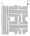
- FIG. 8illustrates a portion of a layout of an SRAM cell 800 being defined using phase shifting.
- the SRAM cell 800is representative of common designs and includes a largely repeating pattern including a portion 810 which is surrounded by a heavy, dashed line.
- FIGS. 9-12show several possible phase layouts for fully defining the layout of FIG. 8 using phase shifting.
- the portion 810is shown with a phase shifting layout.
- the orientation of the cross hatchingindicates the relative phase.
- the phase shifter 912 and the phase shifter 914have opposite phase (X,X+180) as indicated by the different directions of the cross hatching.
- the features defined by the shifters, e.g. feature 916are shown for clarity but are not part of the layout itself.
- the cutting arrangement used in FIG. 9can be described as having a cut in the phase shifters between the two contacts as well as cuts in the inside corners of the T's opposite the cuts between the contacts.
- the particular cutting arrangement usedcause corresponding features, e.g. the feature 916 and the feature 926 , to be defined by a different shifter ordering, e.g. (X, X+180) vs. (X+180, X), as seen by the cross hatching on the shifter 912 , 914 , 922 , and 924 .
- Thismay be undesirable because there can be a light intensity imbalance between for example 0 and 180 degree phase shifters.
- the same featuremay print slightly differently depending on where it fell within the larger pattern of the cell. For example, if the 0 degree phase shifter is slightly more intense than the 180 degree shifter then the light imbalance will tend to move features slightly towards the 180 degree shifter. If the phase ordering is flipped from corresponding feature to corresponding feature then in some cases the features will print slightly to one side and on others slightly to the other side. As such it may be desirable to ensure that the cutting arrangement used to define the individual memory cells of the SRAM is such that the same feature is consistently defined using the same shifter ordering.
- FIG. 10Such an arrangement is shown in FIG. 10 .
- the region 810is shown with a different shifter and cutting arrangement.
- the corresponding featurese.g. the feature 1016 and the feature 1026
- the corresponding featuresare consistently defined using the same phase orderings, e.g. phase shifters 1012 , 1014 , 1022 , and 1024 .
- the cutting arrangement used in FIG. 10can be described as having a cut in the phase shifters between the two contacts as well as cuts on the back of the T's to the adjacent T-back.
- FIG. 11shows a variation on the cutting arrangement of FIG. 10 however, like with FIG. 9 the cutting arrangement causes corresponding features to be defined using alternating phase patterns.
- the cutting arrangement used in FIG. 11can be described as having a cut in the phase shifters from the contact to the field as well as cuts on the back of the T's to the adjacent T-back.
- FIG. 12shows a cutting arrangement that like FIG. 10 ensures that the corresponding features are defined using the same phase ordering.
- the cutting arrangement used in FIG. 12can be described as having cuts in the opposing corners of the T to the contact.
- the particular cutting arrangement selectedwill depend on mask manufacturability concerns, the process design rules, and/or one or more simulations of the cutting arrangement for a given SRAM design and lithographic process.
- the horizontally disposed bars for contacts of adjacent memory cellsare aligned. Specifically instead both a vertical and horizontal offset between bars 812 and bar 814 , the adjacent horizontal bars are in vertical alignment. This would impact the cutting patterns by facilitating the use of straight line cuts between adjacent memory cells, c.f. FIG. 10 and FIG. 11 where a diagonal cut is used.
- phase shiftingcan be used to define other layers of material, e.g. interconnects, metal, etc.
- an angled cutis shown as a preferred cutting arrangement, from a mask manufacturing perspective 90 degree cuts are more easily manufactured. Accordingly, in some embodiments, to the extent practical cuts at 90 degrees to the feature are selected in preference to other cuts. This works well at outside corners where the angled cut can be modified to a straight line cut.
- cut areasare shown as clear regions in fact a gradual, e.g. continuous, phase transition can be used as can a tri- or quad-tone mask, e.g. 0-90-180 or 0-60-120-180, with the middle phase values used in the cut openings.
- Some embodiments of the inventioninclude computer programs for performing the processes of defining the phase shifting layers and/or corresponding trim layers.
- the processis implemented using the abraCAD(TM) software produced by Cadabra Design Automation, a Numerical Technologies company, San Jose, Calif.
- the computer programsare stored in computer readable media, e.g. CD-ROM, DVD, etc.
- the computer programsare embodied in an electromagnetic carrier wave.
- the electromagnetic carrier wavemay include the programs being accessed over a network.
- optical lithographyrefers processes that include the use of visible, ultraviolet, deep ultraviolet, extreme ultraviolet, x-ray, e-beam, and other radiation sources for lithography purposes.
- the masks designs usedshould be appropriately adapted, e.g. reflective vs. transmissive, etc., to the particular lithographic process.
Landscapes
- Physics & Mathematics (AREA)
- General Physics & Mathematics (AREA)
- Preparing Plates And Mask In Photomechanical Process (AREA)
Abstract
Description
This application is related to, claims the benefit of priority of, and incorporates by reference, the U.S. Provisional Patent Application Serial No. 60/296,788 filed Jun. 8, 2001 entitled “Phase Conflict Resolution for Photolithographic Masks” having investors Christophe Pierrat and Michel Côé and assigned to the assignee of the present invention.
This application is related to, claims the benefit of priority of, and incorporates by reference, the U.S. Provisional Patent Application Serial No. 60/304,142 filed Jul. 10, 2001 entitled “Phase Conflict Resolution for Photolithographic Mask” having inventors Christophe Pierrat and Michel Côté and assigned to the assignee of the present invention.
This application is related to, claims the benefit of priority of, and incorporates by reference, the U.S. Provisional Patent Application Serial No. 60/325,689 filed Sep. 28, 2001 entitled “Cost Functions And Gate CD Reduction In Phase Shifting Photolithographic Masks” having inventors Christophe Pierrat and Michel Côté and assigned to the assignee of the present invention.
This application is related to, claims the benefit of priority of, and incorporates by reference, and is a continuation-in-part of the U.S. patent application Ser. No. 09/669,359 filed Sep. 26, 2000 entitled “Phase Shift Masking for Complex Patterns” having inventor Christophe Pierrat and assigned to the assignee of the present invention, which is related to U.S. Provisional Patent Application Serial No. 60/215,938 filed Jul. 5, 2000 entitled “Phase Shift Masking For Complex Layouts” having inventor Christophe Pierrat and assigned to the assignee of the present invention.
1. Field of the Invention
The present invention relates to manufacturing small dimension features of objects, such as integrated circuits, using photolithographic masks. More particularly, the present invention relates to phase shift masking of complex layouts for integrated circuits and similar objects.
2. Description of Related Art
Phase shift masking has been applied to create small dimension features in integrated circuits. Typically the features have been limited to selected elements of the design, which have a small, critical dimension. See, for example, U.S. Pat. No. 5,766,806.
Although manufacturing of small dimension features in integrated circuits has resulted in improved speed and performance, it is desirable to apply phase shift masking more extensively in the manufacturing of such devices. However, the extension of phase shift masking to more complex designs results in a large increase in the complexity of the mask layout problem. For example, when laying out phase shift windows on dense designs, phase conflicts will occur. One type of phase conflict is a location in the layout at which two phase shift windows having the same phase are laid out in proximity to a feature to be exposed by the masks, such as by overlapping of the phase shift windows intended for implementation of adjacent lines in the exposure pattern. If the phase shift windows have the same phase, then they do not result in the optical interference necessary to create the desired feature. Thus, it is necessary to prevent inadvertent layout of phase shift windows in phase conflict near features to be formed in the layer defined by the mask.
In the design of a single integrated circuit, millions of features may be laid out. The burden on data processing resources for iterative operations over such large numbers of features can be huge, and in some cases makes the iterative operation impractical. The layout of phase shift windows and the assignment of phase shift values to such windows, for circuits in which a significant amount of the layout is accomplished by phase shifting, is one such iterative operation which has been impractical using prior art techniques.
Phase shifting layouts for memory cells have been developed that phase shift gate portions of the memory design for improved performance.
Because of these and other complexities, implementation of a phase shift masking technology for complex designs will require improvements in the approach to the design of phase shift masks.
Methods and apparatuses for fully defining static random access memory (SRAM) using phase shifting layouts are described. By producing the SRAM memory using a “full phase” mask, yield can be improved at smaller sizes (relative to using the same lithographic process with a non-phase shifting mask, particularly the wavelength of light, λ), integrated circuit density is improved by tighter packing of smaller memory cells, and also the performance of the memory can be improved.
The approach includes identifying that a layout includes SRAM cells and defining phase shifting regions in a mask description to fully define the SRAM cells. The identification may include an automated detection of layout patterns that correspond to SRAM cells, parameterized shape detection, user identification of SRAM cells either interactively through a user interface and/or through input parameters, and/or other identification approaches.
A region around the layout shapes for an SRAM cell can be identified where phase shifters will be placed in the mask definition. By placing shifters in this region, destructive interference of light of opposite phases will cause definition of the pattern. However, it is necessary to break, or cut, the phase windows in the region to fully permit definition of the feature using phase shifters of opposite phases on opposing edges of the layout shapes of the SRAM cell.
The cuts can be light transmissive phase shifters as well at intermediate phase values (continuous, 90, 60-120) relative to the primary phase shifters (0 and 180).
The portion of the SRAM memory cell layout that is more difficult to define using phase shifting generally comprises two T-shapes (“T′s”) with off-centered bars interlaced with one another. There are contacts at the base of the bars and four transistors on either end of the top of the T. There are two additional transistors disposed above the interlaced T portion.
Several locations where cuts will be admitted are used by embodiments of the invention: contact to contact, inside corners of the T's to field, back of T's to back of adjacent T's, contacts to field, and corners of T's to contacts. By selecting one or more of these cutting locations a phase shifting layout of the SRAM memory cell is possible.
Most mask layouts will select a single cutting pattern for all SRAM memory cells in a particular area. For example, the cutting pattern of using the inside corners of the T's to field together with the back of T's to back of adjacent T's for all SRAM memory cells could be used for all of the SRAM memory cells in a given integrated circuit.
Additionally, attention may be given to ensuring that corresponding features from one SRAM memory cell to another are defined using the same phase ordering. For example if the phase shifter on the left a given transistor is phase 0 and the one on the right is 180, then it may be desirable to ensure that the phase shifter on the left of the corresponding transistor on another SRAM memory cell is 0 and the one on the right is 180. This ensures consistency in the SRAM memory cell layout even if there is a light intensity imbalance between 0 and 180 degree phase shifters.
Embodiments of the invention can be viewed as methods of manufacturing an integrated circuit. Embodiments of the invention include phase shifting and/or complementary trim masks for use in defining a layer of material in a photolithographic process.
The file of this patent contains at least one drawing executed in color. Copies of this patent with color drawing(s) will be provided by the Patent and Trademark Office upon request and payment of the necessary fee.
FIG. 1 illustrates a combination T-L junction.
FIG. 2 illustrates a phase shifting layout for the T-L junction of FIG.1.
FIG. 3 illustrates a squared-U layout with the cutting location indicated for the phase layout.
FIG. 4 illustrates a U layout with the cutting location indicated for the phase layout.
FIG. 5 illustrates a H shaped features with a variety of spacings and phase shift layout arrangements.
FIG. 6 is a simulation of the layout of FIG.5.
FIG. 7 includes portions of the simulation of FIG. 6 at higher magnification.
FIG. 8 illustrates a portion of a layout of an static random access memory (SRAM) cell being defined using phase shifting.
FIGS. 9-12 illustrate different phase layout designs for the SRAM cell of FIG. 8
Overview
Layouts and arrangements for defining several types of patterns using phase shifting will be considered.
T-L Junction
FIG. 1 illustrates a combination T-L junction, specifically the layout of FIG. 1 includes thefeature 100 that includes an L shape adjacent to a T shape. Apreferred shifter area 102 is shown surrounding thefeature 100. Thepreferred shifter area 102 corresponds to the preferred phase shifter width for use in defining thefeature 100 using phase shifting. Further, cutting locations where shifters defined in thepreferred shifter area 102 may be placed. Specifically, thecut locations
FIG. 2 illustrates a phase shifting layout for the T-L junction of FIG.1. More specifically, thecut location 106 was selected—to minimize the number of cuts—and thus four shifters: theshifter 204, theshifter 206, theshifter 208, and theshifter 210, are used to define thefeature 100. The phase shifting layout (and corresponding mask) would include only the shifters. Additionally, a complimentary trim mask for use in conjunction with the layout of FIG. 2 can be developed. See, e.g., U.S. patent application Ser. No. 09/932,239, having inventors Christophe Pierrat, et. al., entitled “Phase Conflict Resolution for Photolithographic Masks”, filed Aug. 17, 2001, and assigned to the assignee of the present application, which is incorporated herein by reference.
U Shapes
Turning to FIGS. 3-4, two U-shaped layouts are shown. FIG. 3 illustrates a squared-U layout with the cutting location indicated for the phase layout. FIG. 4 illustrates a U layout with the cutting location indicated for the phase layout. In each, a single cut on the inside of the U will be used to separate the phase shifters (a corresponding cut can be used on the outside of the U).
Specifically, FIG. 3 includes thefeature 300 and thefeature 302. Asingle cut 304 extends from interior of the corner of thefeature 300 towards thefeature 302 and then runs parallel along the endcap of thefeature 302. Similarly, in FIG. 4 thefeature 400 and feature402 comprise the layout pattern and acut 404 is used in the interior. Additionally, with respect to FIG. 4, in some embodiments a slightly different cut shape is used in the interior bend of the U. Specifically, acorner 410 and acorner 412 are shown interior to the bended U. In some embodiments, the cut is centered about one of the two corners rather than the full length of the interior angled wall of the U.
H-Shapes
FIG. 5 includes a test pattern for H-shapes arranged in a 12 wide by 5 high grid. There are twelve different spacings between the vertical bars of the H shown across FIG.5 and for each spacing, the column shows a possible shifter arrangement for that spacing. For clarity of reference, each H pattern can be referred to by its x-y position, e.g. (1,1) being the upper leftmost H and (12,5) being the bottom rightmost H. Thus, within a row the space between the bars of the H wider for the H (j′,k) as compared to the H (j,k) where j′>j.
Which option is ultimately selected will depend on the surrounding environment, e.g. the adjacent polygons, as well as the process latitude. For example, the H shapes in the first row (1,1) . . . (12,1) are premised on the assumption that it will be possible to make a cut on both sides of the H. In contrast the H shapes in the second row assume only one cut is possible, e.g. H's (1,2) . . . (12,2). The remaining rows make no use of cuts on the outside of the H. But, may result in difficult to manufacture masks, e.g. H (5,3) which has a small phase shift area. Other patterns may allow the phase conflict by not using any cuts, H's (1,5) . . . (12,5). It should be noted that some of the H patterns in rows two through four lack adequate space to admit the cutting pattern used in the remainder of the row, c.f. H's (1,2) . . . (4,2), (1,3) . . . (4,3), and (1,4) . . . (4,4) with the remaining H's in those rows.
In FIG. 6, a simulated aerial image of the test pattern of FIG. 5 is shown. The exposure conditions assumed that the phase shift mask was exposed with a 248 nm wavelength (λ) light, N.A.=0.75, and σ=0.5 and that the trim mask (not shown) was exposed using the same λ and N.A., but with σ=0.5 and three times the dosage. As can be seen from the simulation in most cases the layouts will be correctable with optical proximity correction. However, there will be a resulting impact on process latitude. For example, the H (6,2) and the H (7,2) can likely print however there will be a limited amount of process latitude for the vertical lines. Similar problem, e.g. with H (5,4), but note that other H's in row four are more likely to be correctable with OPC, e.g. H's (8,4) . . . (12,4). In contrast note that in row five, the bars of the smaller H's are more easily corrected with OPC across the phase conflict, e.g. H's (1,5) . . . (4.5), while in contrast as the length of the phase conflict area increases correction with OPC becomes more difficult or perhaps impossible, e.g. H's (5,5) . . . (12,5).
Turning to FIG. 7, a magnified view of the simulations for one of the columns, j, at separation 0.5 μm, is shown with the magnified images arranged sideways (e.g. top most row on the left, bottom most row on the right). As shown OPC correction can be applied in the OPC cutregions 710 and thephase conflict region 720. In some instances there may be insufficient process latitude to reliably print the feature, e.g. (j,5) may lack sufficient process latitude to reliably print on the wafer even with optical proximity correction.
SRAM Cutting
FIG. 8 illustrates a portion of a layout of anSRAM cell 800 being defined using phase shifting. TheSRAM cell 800 is representative of common designs and includes a largely repeating pattern including aportion 810 which is surrounded by a heavy, dashed line. FIGS. 9-12 show several possible phase layouts for fully defining the layout of FIG. 8 using phase shifting.
Turning to FIG. 9, theportion 810 is shown with a phase shifting layout. The orientation of the cross hatching indicates the relative phase. For example, the phase shifter912 and thephase shifter 914 have opposite phase (X,X+180) as indicated by the different directions of the cross hatching. The features defined by the shifters, e.g. feature916, are shown for clarity but are not part of the layout itself.
The cutting arrangement used in FIG. 9 can be described as having a cut in the phase shifters between the two contacts as well as cuts in the inside corners of the T's opposite the cuts between the contacts.
As can be seen in FIG. 9, the particular cutting arrangement used cause corresponding features, e.g. the feature916 and the feature926, to be defined by a different shifter ordering, e.g. (X, X+180) vs. (X+180, X), as seen by the cross hatching on theshifter
Thus, the same feature may print slightly differently depending on where it fell within the larger pattern of the cell. For example, if the 0 degree phase shifter is slightly more intense than the 180 degree shifter then the light imbalance will tend to move features slightly towards the 180 degree shifter. If the phase ordering is flipped from corresponding feature to corresponding feature then in some cases the features will print slightly to one side and on others slightly to the other side. As such it may be desirable to ensure that the cutting arrangement used to define the individual memory cells of the SRAM is such that the same feature is consistently defined using the same shifter ordering.
Such an arrangement is shown in FIG.10. Specifically, theregion 810 is shown with a different shifter and cutting arrangement. Here, the corresponding features, e.g. the feature1016 and the feature1026, are consistently defined using the same phase orderings, e.g. phase shifters1012,1014,1022, and1024.
The cutting arrangement used in FIG. 10 can be described as having a cut in the phase shifters between the two contacts as well as cuts on the back of the T's to the adjacent T-back.
FIG. 11 shows a variation on the cutting arrangement of FIG. 10 however, like with FIG. 9 the cutting arrangement causes corresponding features to be defined using alternating phase patterns.
The cutting arrangement used in FIG. 11 can be described as having a cut in the phase shifters from the contact to the field as well as cuts on the back of the T's to the adjacent T-back.
FIG. 12 shows a cutting arrangement that like FIG. 10 ensures that the corresponding features are defined using the same phase ordering.
The cutting arrangement used in FIG. 12 can be described as having cuts in the opposing corners of the T to the contact.
The particular cutting arrangement selected will depend on mask manufacturability concerns, the process design rules, and/or one or more simulations of the cutting arrangement for a given SRAM design and lithographic process.
It should also be noted that in some memory designs the horizontally disposed bars for contacts of adjacent memory cells are aligned. Specifically instead both a vertical and horizontal offset betweenbars 812 andbar 814, the adjacent horizontal bars are in vertical alignment. This would impact the cutting patterns by facilitating the use of straight line cuts between adjacent memory cells, c.f. FIG.10 and FIG. 11 where a diagonal cut is used.
Representative Alternative Embodiments
Additionally, although the description has primarily focused on examples of defining a polysilicon, or “poly”, layer within an IC, phase shifting can be used to define other layers of material, e.g. interconnects, metal, etc.
Although in many instances, an angled cut is shown as a preferred cutting arrangement, from a mask manufacturing perspective 90 degree cuts are more easily manufactured. Accordingly, in some embodiments, to the extent practical cuts at 90 degrees to the feature are selected in preference to other cuts. This works well at outside corners where the angled cut can be modified to a straight line cut.
Although the cut areas are shown as clear regions in fact a gradual, e.g. continuous, phase transition can be used as can a tri- or quad-tone mask, e.g. 0-90-180 or 0-60-120-180, with the middle phase values used in the cut openings.
Some embodiments of the invention include computer programs for performing the processes of defining the phase shifting layers and/or corresponding trim layers. In one embodiment, the process is implemented using the abraCAD(™) software produced by Cadabra Design Automation, a Numerical Technologies company, San Jose, Calif. In some embodiments, the computer programs are stored in computer readable media, e.g. CD-ROM, DVD, etc. In other embodiments, the computer programs are embodied in an electromagnetic carrier wave. For example, the electromagnetic carrier wave may include the programs being accessed over a network.
As used herein, the term optical lithography refers processes that include the use of visible, ultraviolet, deep ultraviolet, extreme ultraviolet, x-ray, e-beam, and other radiation sources for lithography purposes. The masks designs used should be appropriately adapted, e.g. reflective vs. transmissive, etc., to the particular lithographic process.
Conclusion
The foregoing description of embodiments of the invention has been provided for the purposes of illustration and description. It is not intended to be exhaustive or to limit the invention to the precise form disclosed. Many modifications and variations will be apparent. The embodiments were chosen and described in order to best explain the principles of the invention and its practical application, thereby enabling others to understand the invention for various embodiments and with various modifications as are suited to the particular use contemplated. It is intended that the scope of the invention be defined by the following claims.
Claims (24)
1. A method for producing a computer readable definition of a photolithographic mask that defines a pattern in a layer to be formed using the mask, wherein the pattern includes a plurality of features corresponding to a plurality of static random access memory (SRAM) cells, the plurality of features including two opposing T-shapes in a field for each SRAM cell, the T-shapes generally shaped like a T, a T-shape having a top with a back, and a bar, the top and the bar forming inside comas, and having a contact on the bar, the method comprising:
selecting a cutting pattern from a set of patterns including at least
(i) a first cutting pattern comprising a first cut between two contacts of each SRAM cell and a second and third cuts, the second and third cuts on inside corners of the T-shapes of each SRAM cell opposite the first cut,
(ii) a second cutting pattern comprising a first cut between two contacts of each SRAM cell and a second cut on the back of the T-shape of each SRAM cell to the back of a T-shape of an adjacent SRAM cell,
(iii) a third cutting pattern comprising a first cut and a second cut from contacts of the SRAM cell to the field and a third cut on the back of the T-shape of the SRAM cell to the back of a T-shape of an adjacent SRAM, and
(iv) a fourth cutting pattern comprising a first cut and a second cut extending respectively from opposing inside corners of one of the two T-shapes of each SRAM cell to the contacts on the bars of the other of the two T-shapes of each SRAM cell,
for use in defining the plurality of SRAM cells; and
defining a plurality of phase shifters in the computer readable definition of the mask to fully define the plurality of SRAM cells using destructive light interference, wherein the plurality of phase shifters separated by cuts according to the cutting pattern.
2. The method ofclaim 1 , wherein the plurality of features have a first gate critical dimension, and wherein the defining a plurality of phase shifters further comprises defining the plurality of phase shifters such that the gate critical dimension less then the first gate critical dimension.
3. The method ofclaim 1 , further comprising defining a computer readable definition of a second mask, the second mask comprising a complementary trim mask for use in conjunction with the mask and for preserving structure defined by the mask and clearing artifacts created by use of the mask.
4. The method ofclaim 3 , further comprising manufacturing a photolithographic mask using the computer readable definition of the mask and the computer readable definition of the second mask.
5. The method ofclaim 1 , wherein the pattern corresponds to a pattern for an SRAM memory chip.
6. A method of manufacturing an integrated circuit product, the method comprising:
identifying a pattern comprised of a plurality of features in a description of a layer of material in the integrated circuit, the pattern corresponding to a plurality of SRAM cells, the plurality of features including two opposing T-shapes in a field for each SRAM cell, the T-shapes generally shaped like a T, a T-shape having a top with a back, and a bar, the top and the bar forming inside corners, and having a contact on the bar;
defining a computer readable definition of a first mask, the first mask comprised of a plurality of phase shifters disposed on an opaque field, the phase shifters disposed such that destructive light interference between adjacent phase shifters defines the pattern, wherein the disposition of the phase shifters according to cuts between locations in the pattern corresponding to one or more of contacts to contacts, back of a T-shape to back of an adjacent T-shape, contacts to inside corners of T-shapes, contacts to field, and inside corners of T-shapes to field;
defining a computer readable definition of a second mask, the second mask including protective opaque regions on a clear field for protecting the pattern defined using the first mask and clearing artifacts created by the first mask; and
defining a layer of material in the integrated circuit using a mask produced from the computer readable definition of the first mask and the computer readable definition of the second mask.
7. The method ofclaim 6 , wherein the integrated circuit comprises an SRAM memory chip.
8. The method ofclaim 6 , wherein the cuts defined such that corresponding structures of different SRAM cells consistently defined using a particular phase ordering.
9. The method ofclaim 8 , wherein the cuts comprise contact to contact and back of T-shape to back of an adjacent T-shape cut.
10. The method ofclaim 6 , wherein the cuts comprise phase shifting regions of phase different from those used by the plurality of phase shifters.
11. The method ofclaim 10 , wherein the cut regions have phase 60 degrees and 120 degrees relative to said phase shifters.
12. The method ofclaim 10 , wherein the cut regions have phase 90 degrees relative to said phase shifters.
13. A photolithographic mask for defining a layer of material, the layer of material including a pattern, the pattern corresponding to a plurality of SRAM cells, the photolithographic mask comprising a dark field mask with a plurality of light transmissive phase shifting regions disposed therein, the disposition of the phase shifting regions such that destructive light interference between the light transmissive phase shifting regions defines the plurality of SRAM cells, the plurality of features including two opposing T-shapes in a field for each SRAM cell, the T-shapes generally shaped like a T, a T-shape having a top with a back, and a bar, the top and the bar forming inside corners, and having a contact on the bar, and according to cuts between locations in the pattern corresponding to one or more of contacts to contacts, back of a T-shape to back of an adjacent T-shape, contacts to inside corners of T-shapes, contacts to field, and inside corners of T-shapes to field.
14. The mask ofclaim 13 , wherein the mask for use in defining a layer of material for an SRAM memory chip.
15. The mask ofclaim 13 , wherein substantially all of the structure of each of the plurality of SRAM cells defined by the destructive interference created by the positioning of the phase shifting regions.
16. An apparatus for creating computer readable definition of a mask, the apparatus comprising:
means for identifying a pattern, the pattern comprising a plurality of SRAM memory cells in a layout, SRAM memory cells including two opposing T-shapes in a field for each SRAM cell, the T-shapes generally shaped like a T, a T-shape having a top with a back, and a bar, the top and the bar forming inside corners, and having a contact on the bar; means for defining a phase shifting region around the pattern, and
means for dividing the phase shifting region into a plurality of phase shifters for defining the pattern such that the pattern is fully defined using the plurality of phase shifters, and the phase shifters divided by a plurality of cuts between one or more of locations in the pattern corresponding to one or more of contacts to contacts, back of a T-shape to back of an adjacent T-shape, contacts to inside corners of T-shapes, contacts to field, and inside corners of T-shapes to field.
17. The apparatus ofclaim 16 , wherein the mask for use in defining a layer of material for an SRAM memory chip.
18. The apparatus ofclaim 16 , further comprising means for defining a computer readable definition of a complimentary mask, the complimentary mask for use in conjunction with the mask to protect the pattern defined using the mask and to clear artifacts created by the first mask.
19. The apparatus ofclaim 16 , wherein the cuts comprise phase shifting regions having intermediate phase angles relative to the plurality of phase shifters.
20. A method for producing a computer readable definition of a photolithographic mask that defines a pattern in a layer to be formed using the mask, wherein the pattern includes a plurality of features corresponding to a plurality of static random access memory (SRAM) cells, the plurality of features including two opposing T-shapes in a field for each SRAM cell, the T-shapes generally shaped like a T, a T-shape having a ton with a back, and a bar, the top and the bar forming inside corners, and having a contact on the bar, the method comprising defining a plurality of phase shifters in the computer readable definition of the mask to fully define the plurality of SRAM cells using destructive light interference, wherein the plurality of phase shifters separated by cuts comprised of a first cut between two contacts of each SRAM cell and second and third cuts, the second and third cuts on inside corners of T-shapes of each SRAM cell opposite the first cut.
21. A method for producing a computer readable definition of a photolithographic mask that defines a pattern in a layer to be formed using the mask, wherein the pattern includes a plurality of features corresponding to a plurality of static random access memory (SRAM) cells, the plurality of features including two opposing T-shapes in a field for each SRAM cell, the T-shapes generally shaped like a T, a T-shape having a top with a back, and a bar, the top and the bar forming inside corners, and having a contact on the bar, the method comprising defining a plurality of phase shifters in the computer readable definition of the mask to fully define the plurality of SRAM cells using destructive light interference, wherein the plurality of phase shifters separated by cuts comprised of a first cut between two contacts of each SRAM cell and a second cut on back of a T-shape of each SRAM cell to back of a T-shape of an adjacent SRAM cell.
22. A method for producing a computer readable definition of a photolithographic mask that defines a pattern in a layer to be formed using the mask, wherein the pattern includes a plurality of features corresponding to a plurality of static random access memory (SRAM) cells, the plurality of features including two opposing T-shapes in a field for each SRAM cell, the T-shapes generally shaped like a T, a T-shape having a top with a back, and a bar, the top and the bar forming inside corners, and having a contact on the bar, the method comprising defining a plurality of phase shifters in the computer readable definition of the mask to fully define the plurality of SRAM cells using destructive light interference, wherein the plurality of phase shifters separated by cuts comprised of a first cut and second cut from contacts of an SRAM cell to field and a third cut from a back of a T-shape of the SRAM cell to back of a T-shape of an adjacent SRAM cell.
23. A method for producing a computer readable definition of a photolithographic mask that defines a pattern in a layer to be formed using the mask, wherein the pattern includes a plurality of features corresponding to a plurality of static random access memory (SRAM) cells, the plurality of features including two opposing T-shapes in a field for each SRAM cell, the T-shapes generally shaped like a T, a T-shape having a top with a back, and a bar, the top and the bar forming inside corners, and having a contact on the bar the method comprising defining a plurality of phase shifters in the computer readable definition of the mask to fully define the plurality of SRAM cells using destructive light interference, wherein the plurality of phase shifters separated by cuts comprised of a first cut and a second cut in opposing corners of the T-shapes of each SRAM cell to contacts.
24. An electromagnetic wave form comprising a computer program, the computer program for defining a mask layout, the computer program comprising:
a first set of instructions for identifying a pattern comprised of a plurality of features in a description of a layer of material in the integrated circuit, the pattern corresponding to a plurality of SRAM cells, the plurality of features including two opposing T-shapes in a field for each SRAM cell, the T-shapes generally shaped like a T, a T-shape having a top with a back, and a bar, the toy and the bar forming inside corners and having a contact on the bar;
a second set of instructions for defining a computer readable definition of a first mask, the first mask comprised of a plurality of phase shifters disposed on an opaque field, the phase shifters disposed such that destructive light interference between adjacent phase shifters defines the pattern, wherein the disposition of the phase shifters according to cuts between locations in the pattern corresponding to one or more of contacts to contacts back of a T-shape to back of an adjacent T-shape, contacts to inside corners of T-shapes, contacts to field, and inside corners of T-shapes to field;
a third set of instructions for defining a computer readable definition of a second mask, the second mask including protective opaque regions on a clear field for protecting the pattern defined using the first mask and clearing artifacts created by the first mask; and
a fourth set of instructions for defining a layer of material in the integrated circuit using a mask produced from the computer readable definition of the first mask and the computer readable definition of the second mask.
Priority Applications (2)
| Application Number | Priority Date | Filing Date | Title |
|---|---|---|---|
| US09/996,973US6681379B2 (en) | 2000-07-05 | 2001-11-15 | Phase shifting design and layout for static random access memory |
| US10/340,377US6981240B2 (en) | 2001-11-15 | 2003-01-10 | Cutting patterns for full phase shifting masks |
Applications Claiming Priority (6)
| Application Number | Priority Date | Filing Date | Title |
|---|---|---|---|
| US21593800P | 2000-07-05 | 2000-07-05 | |
| US09/669,359US6503666B1 (en) | 2000-07-05 | 2000-09-26 | Phase shift masking for complex patterns |
| US29678801P | 2001-06-08 | 2001-06-08 | |
| US30414201P | 2001-07-10 | 2001-07-10 | |
| US32568901P | 2001-09-28 | 2001-09-28 | |
| US09/996,973US6681379B2 (en) | 2000-07-05 | 2001-11-15 | Phase shifting design and layout for static random access memory |
Related Parent Applications (1)
| Application Number | Title | Priority Date | Filing Date |
|---|---|---|---|
| US09/669,359Continuation-In-PartUS6503666B1 (en) | 2000-07-05 | 2000-09-26 | Phase shift masking for complex patterns |
Related Child Applications (1)
| Application Number | Title | Priority Date | Filing Date |
|---|---|---|---|
| US10/340,377Continuation-In-PartUS6981240B2 (en) | 2001-11-15 | 2003-01-10 | Cutting patterns for full phase shifting masks |
Publications (2)
| Publication Number | Publication Date |
|---|---|
| US20020129327A1 US20020129327A1 (en) | 2002-09-12 |
| US6681379B2true US6681379B2 (en) | 2004-01-20 |
Family
ID=46204312
Family Applications (1)
| Application Number | Title | Priority Date | Filing Date |
|---|---|---|---|
| US09/996,973Expired - LifetimeUS6681379B2 (en) | 2000-07-05 | 2001-11-15 | Phase shifting design and layout for static random access memory |
Country Status (1)
| Country | Link |
|---|---|
| US (1) | US6681379B2 (en) |
Cited By (13)
| Publication number | Priority date | Publication date | Assignee | Title |
|---|---|---|---|---|
| US20040073884A1 (en)* | 2002-10-09 | 2004-04-15 | Numerical Technologies, Inc. | Phase shifting mask topography effect correction based on near-field image properties |
| US20050076321A1 (en)* | 2002-01-18 | 2005-04-07 | Smith Bruce W. | Method of photomask correction and its optimization using localized frequency analysis |
| US20050095512A1 (en)* | 2003-08-29 | 2005-05-05 | Molela Moukara | Lithography mask for imaging of convex structures |
| US20050210436A1 (en)* | 2004-03-18 | 2005-09-22 | International Business Machines Corporation | Alternating phase-shift mask rule compliant ic design |
| US20070190431A1 (en)* | 2006-02-10 | 2007-08-16 | Chun-Chung Huang | Photomask structure |
| US20080148217A1 (en)* | 2006-12-13 | 2008-06-19 | Jea-Woo Park | Selective shielding for multiple exposure masks |
| US20080166639A1 (en)* | 2007-01-08 | 2008-07-10 | Jea-Woo Park | Data preparation for multiple mask printing |
| US20080307381A1 (en)* | 2007-06-05 | 2008-12-11 | Alexander Tritchkov | Ic layout parsing for multiple masks |
| US20090101983A1 (en)* | 2007-10-18 | 2009-04-23 | Texas Instruments Incorporated | Method of Achieving Dense-Pitch Interconnect Patterning in Integrated Circuits |
| US20100050149A1 (en)* | 2000-07-05 | 2010-02-25 | Synopsys, Inc. | Design and Layout of Phase Shifting Photolithographic Masks |
| US20100162193A1 (en)* | 2004-11-04 | 2010-06-24 | Pileggi Lawrence T | Method and process for design of integrated circuits using regular geometry patterns to obtain geometrically consistent component features |
| US20110318673A1 (en)* | 2010-03-12 | 2011-12-29 | Semiconductor Manufacturing International (Shanghai) Corporation | System and method for test pattern for lithography process |
| US11996364B2 (en) | 2021-04-16 | 2024-05-28 | Samsung Electronics Co., Ltd. | Integrated circuit chip including gate electrode with oblique cut surface, and manufacturing method of the same |
Families Citing this family (33)
| Publication number | Priority date | Publication date | Assignee | Title |
|---|---|---|---|---|
| US6811935B2 (en)* | 2000-07-05 | 2004-11-02 | Numerical Technologies, Inc. | Phase shift mask layout process for patterns including intersecting line segments |
| US6681379B2 (en) | 2000-07-05 | 2004-01-20 | Numerical Technologies, Inc. | Phase shifting design and layout for static random access memory |
| US6978436B2 (en)* | 2000-07-05 | 2005-12-20 | Synopsys, Inc. | Design data format and hierarchy management for phase processing |
| US6733929B2 (en) | 2000-07-05 | 2004-05-11 | Numerical Technologies, Inc. | Phase shift masking for complex patterns with proximity adjustments |
| US7028285B2 (en)* | 2000-07-05 | 2006-04-11 | Synopsys, Inc. | Standard cell design incorporating phase information |
| US7083879B2 (en)* | 2001-06-08 | 2006-08-01 | Synopsys, Inc. | Phase conflict resolution for photolithographic masks |
| US6777141B2 (en) | 2000-07-05 | 2004-08-17 | Numerical Technologies, Inc. | Phase shift mask including sub-resolution assist features for isolated spaces |
| US6524752B1 (en) | 2000-07-05 | 2003-02-25 | Numerical Technologies, Inc. | Phase shift masking for intersecting lines |
| US6866971B2 (en) | 2000-09-26 | 2005-03-15 | Synopsys, Inc. | Full phase shifting mask in damascene process |
| US6901575B2 (en) | 2000-10-25 | 2005-05-31 | Numerical Technologies, Inc. | Resolving phase-shift conflicts in layouts using weighted links between phase shifters |
| US6584610B1 (en) | 2000-10-25 | 2003-06-24 | Numerical Technologies, Inc. | Incrementally resolved phase-shift conflicts in layouts for phase-shifted features |
| US6622288B1 (en) | 2000-10-25 | 2003-09-16 | Numerical Technologies, Inc. | Conflict sensitive compaction for resolving phase-shift conflicts in layouts for phase-shifted features |
| US6728946B1 (en)* | 2000-10-31 | 2004-04-27 | Franklin M. Schellenberg | Method and apparatus for creating photolithographic masks |
| US6846596B2 (en)* | 2001-03-08 | 2005-01-25 | Numerical Technologies, Inc. | Alternating phase shift masking for multiple levels of masking resolution |
| US6635393B2 (en) | 2001-03-23 | 2003-10-21 | Numerical Technologies, Inc. | Blank for alternating PSM photomask with charge dissipation layer |
| US6566019B2 (en) | 2001-04-03 | 2003-05-20 | Numerical Technologies, Inc. | Using double exposure effects during phase shifting to control line end shortening |
| US6553560B2 (en)* | 2001-04-03 | 2003-04-22 | Numerical Technologies, Inc. | Alleviating line end shortening in transistor endcaps by extending phase shifters |
| US6573010B2 (en) | 2001-04-03 | 2003-06-03 | Numerical Technologies, Inc. | Method and apparatus for reducing incidental exposure by using a phase shifter with a variable regulator |
| US6593038B2 (en) | 2001-05-04 | 2003-07-15 | Numerical Technologies, Inc. | Method and apparatus for reducing color conflicts during trim generation for phase shifters |
| US6569583B2 (en) | 2001-05-04 | 2003-05-27 | Numerical Technologies, Inc. | Method and apparatus for using phase shifter cutbacks to resolve phase shifter conflicts |
| US6852471B2 (en) | 2001-06-08 | 2005-02-08 | Numerical Technologies, Inc. | Exposure control for phase shifting photolithographic masks |
| US7178128B2 (en)* | 2001-07-13 | 2007-02-13 | Synopsys Inc. | Alternating phase shift mask design conflict resolution |
| US6664009B2 (en) | 2001-07-27 | 2003-12-16 | Numerical Technologies, Inc. | Method and apparatus for allowing phase conflicts in phase shifting mask and chromeless phase edges |
| US6738958B2 (en) | 2001-09-10 | 2004-05-18 | Numerical Technologies, Inc. | Modifying a hierarchical representation of a circuit to process composite gates |
| US6698007B2 (en) | 2001-10-09 | 2004-02-24 | Numerical Technologies, Inc. | Method and apparatus for resolving coloring conflicts between phase shifters |
| US6981240B2 (en) | 2001-11-15 | 2005-12-27 | Synopsys, Inc. | Cutting patterns for full phase shifting masks |
| US7122281B2 (en)* | 2002-02-26 | 2006-10-17 | Synopsys, Inc. | Critical dimension control using full phase and trim masks |
| US6605481B1 (en) | 2002-03-08 | 2003-08-12 | Numerical Technologies, Inc. | Facilitating an adjustable level of phase shifting during an optical lithography process for manufacturing an integrated circuit |
| US6704921B2 (en) | 2002-04-03 | 2004-03-09 | Numerical Technologies, Inc. | Automated flow in PSM phase assignment |
| US6785879B2 (en)* | 2002-06-11 | 2004-08-31 | Numerical Technologies, Inc. | Model-based data conversion |
| US6821689B2 (en) | 2002-09-16 | 2004-11-23 | Numerical Technologies | Using second exposure to assist a PSM exposure in printing a tight space adjacent to large feature |
| US7421676B2 (en)* | 2004-09-15 | 2008-09-02 | Chartered Semiconductor Manufacturing Ltd. | System and method for phase shift assignment |
| US8426114B2 (en)* | 2011-01-28 | 2013-04-23 | Infineon Technologies Ag | L-shaped feature, method of making an L-shaped feature and method of making an L-shaped structure |
Citations (68)
| Publication number | Priority date | Publication date | Assignee | Title |
|---|---|---|---|---|
| US4037918A (en) | 1974-08-03 | 1977-07-26 | Matsushita Electric Industrial Co., Ltd. | Fourier-transform holography by pseudo-random phase shifting |
| US4456371A (en) | 1982-06-30 | 1984-06-26 | International Business Machines Corporation | Optical projection printing threshold leveling arrangement |
| JPS6267547A (en) | 1985-09-20 | 1987-03-27 | Hitachi Ltd | photomask |
| JPH02140743A (en) | 1988-11-22 | 1990-05-30 | Hitachi Ltd | Method of manufacturing integrated circuit device |
| EP0464492A1 (en) | 1990-06-21 | 1992-01-08 | Matsushita Electronics Corporation | A photomask used by photolithography and a process of producing the same |
| JPH0667403A (en) | 1992-03-27 | 1994-03-11 | Nippon Telegr & Teleph Corp <Ntt> | Photomask and method for processing mask pattern data |
| US5296729A (en)* | 1990-10-26 | 1994-03-22 | Hitachi, Ltd. | Semiconductor memory device having static random access memory |
| US5302477A (en) | 1992-08-21 | 1994-04-12 | Intel Corporation | Inverted phase-shifted reticle |
| US5308741A (en) | 1992-07-31 | 1994-05-03 | Motorola, Inc. | Lithographic method using double exposure techniques, mask position shifting and light phase shifting |
| US5316878A (en) | 1991-06-19 | 1994-05-31 | Oki Electric Industry Co., Ltd. | Pattern forming method and photomasks used therefor |
| US5324600A (en) | 1991-07-12 | 1994-06-28 | Oki Electric Industry Co., Ltd. | Method of forming resist pattern and photomask therefor |
| US5328807A (en) | 1990-06-11 | 1994-07-12 | Hitichi, Ltd. | Method of forming a pattern |
| US5334542A (en) | 1991-11-27 | 1994-08-02 | Oki Electric Industry Co., Ltd. | Method of forming T-shaped electrode |
| US5364716A (en) | 1991-09-27 | 1994-11-15 | Fujitsu Limited | Pattern exposing method using phase shift and mask used therefor |
| JPH07111528A (en) | 1993-10-12 | 1995-04-25 | Matsushita Electric Ind Co Ltd | Answering machine |
| EP0653679A2 (en) | 1989-04-28 | 1995-05-17 | Fujitsu Limited | Mask, mask producing method and pattern forming method using mask |
| US5424154A (en) | 1993-12-10 | 1995-06-13 | Intel Corporation | Lithographic emhancement method and apparatus for randomly spaced structures |
| US5472814A (en) | 1994-11-17 | 1995-12-05 | International Business Machines Corporation | Orthogonally separated phase shifted and unphase shifted mask patterns for image improvement |
| US5480746A (en) | 1991-10-01 | 1996-01-02 | Oki Electric Industry Co., Ltd. | Photomask and method of forming resist pattern using the same |
| JPH0851068A (en) | 1995-05-10 | 1996-02-20 | Hitachi Ltd | Mask formation method |
| EP0698821A1 (en) | 1994-08-03 | 1996-02-28 | International Business Machines Corporation | High resolution phase edge lithography without the need for a trim mask |
| US5496666A (en) | 1994-10-27 | 1996-03-05 | Chartered Semiconductor Manufacturing Pte Ltd. | Contact hole mask for semiconductor fabrication |
| US5503951A (en) | 1994-02-14 | 1996-04-02 | International Business Machines Corp. | Attenuating phase-shift mask structure and fabrication method |
| US5523186A (en) | 1994-12-16 | 1996-06-04 | International Business Machines Corporation | Split and cover technique for phase shifting photolithography |
| DE19545163A1 (en) | 1994-12-02 | 1996-06-05 | Hyundai Electronics Ind | Phase shift mask for the formation of contact holes with micro dimensions |
| US5527645A (en) | 1993-04-21 | 1996-06-18 | Pati; Yagyensh C. | Systematic method for production of phase-shifting photolithographic masks |
| US5532090A (en) | 1995-03-01 | 1996-07-02 | Intel Corporation | Method and apparatus for enhanced contact and via lithography |
| US5537648A (en) | 1994-08-15 | 1996-07-16 | International Business Machines Corporation | Geometric autogeneration of "hard" phase-shift designs for VLSI |
| US5539568A (en) | 1994-06-16 | 1996-07-23 | Texas Instruments Incorporated | Method of exposing a light sensitive material |
| US5538815A (en) | 1992-09-14 | 1996-07-23 | Kabushiki Kaisha Toshiba | Method for designing phase-shifting masks with automatization capability |
| JPH08236317A (en) | 1995-02-24 | 1996-09-13 | Alps Electric Co Ltd | Motor driven sliding type variable resistor |
| US5565286A (en) | 1994-11-17 | 1996-10-15 | International Business Machines Corporation | Combined attenuated-alternating phase shifting mask structure and fabrication methods therefor |
| US5573890A (en) | 1994-07-18 | 1996-11-12 | Advanced Micro Devices, Inc. | Method of optical lithography using phase shift masking |
| US5595843A (en) | 1995-03-30 | 1997-01-21 | Intel Corporation | Layout methodology, mask set, and patterning method for phase-shifting lithography |
| US5725969A (en) | 1995-09-25 | 1998-03-10 | Lg Semicon Co., Ltd. | Method of manufacturing phase-shifting mask comprising a light shield pattern on a phase-shifting attenuatting layer |
| WO1998012605A1 (en) | 1996-09-18 | 1998-03-26 | Numerical Technologies, Inc. | Phase shifting circuit manufacture method and apparatus |
| JPH10133356A (en) | 1996-09-06 | 1998-05-22 | Matsushita Electric Ind Co Ltd | Photomask and pattern forming method |
| US5761075A (en) | 1993-12-28 | 1998-06-02 | Kabushiki Kaisha Toshiba | Apparatus for designing photomasks |
| US5807649A (en) | 1996-10-31 | 1998-09-15 | International Business Machines Corporation | Lithographic patterning method and mask set therefor with light field trim mask |
| US5827623A (en) | 1995-10-31 | 1998-10-27 | Nec Corporation | Optical proximity correction halftone type phase shift photomask |
| US5858580A (en) | 1997-09-17 | 1999-01-12 | Numerical Technologies, Inc. | Phase shifting circuit manufacture method and apparatus |
| US5885734A (en) | 1996-08-15 | 1999-03-23 | Micron Technology, Inc. | Process for modifying a hierarchical mask layout |
| JPH11143085A (en) | 1997-11-06 | 1999-05-28 | Canon Inc | Exposure method and exposure apparatus |
| US5923562A (en) | 1996-10-18 | 1999-07-13 | International Business Machines Corporation | Method for automatically eliminating three way intersection design conflicts in phase edge, phase shift designs |
| US5923566A (en) | 1997-03-25 | 1999-07-13 | International Business Machines Corporation | Phase shifted design verification routine |
| GB2333613A (en) | 1998-01-23 | 1999-07-28 | Sony Corp | Mask pattern generating method |
| US5994002A (en) | 1996-09-06 | 1999-11-30 | Matsushita Electric Industrial Co., Ltd. | Photo mask and pattern forming method |
| US5998068A (en) | 1997-01-28 | 1999-12-07 | Matsushita Electric Industrial Co., Ltd. | Reticle and pattern formation method |
| US6004702A (en) | 1997-11-28 | 1999-12-21 | United Microelectronics Corp. | Phase-shifting mask structure and method of fabricating the same |
| US6010807A (en) | 1997-11-22 | 2000-01-04 | United Microelectronics Corp. | Phase-shifting mask for photolithography in semiconductor fabrications |
| US6057063A (en) | 1997-04-14 | 2000-05-02 | International Business Machines Corporation | Phase shifted mask design system, phase shifted mask and VLSI circuit devices manufactured therewith |
| US6066180A (en) | 1997-03-04 | 2000-05-23 | International Business Machines Corporation | Automatic generation of phase shift masks using net coloring |
| US6077630A (en) | 1998-01-08 | 2000-06-20 | Micron Technology, Inc. | Subresolution grating for attenuated phase shifting mask fabrication |
| US6083275A (en) | 1998-01-09 | 2000-07-04 | International Business Machines Corporation | Optimized phase shift design migration |
| US6130012A (en) | 1999-01-13 | 2000-10-10 | Advanced Micro Devices, Inc. | Ion beam milling to generate custom reticles |
| US6139994A (en) | 1999-06-25 | 2000-10-31 | Broeke; Doug Van Den | Use of intersecting subresolution features for microlithography |
| US6185727B1 (en) | 1995-12-12 | 2001-02-06 | International Business Machines Corporation | Design verification for asymmetric phase shift mask layouts |
| WO2001023961A1 (en) | 1999-09-28 | 2001-04-05 | Mentor Graphics Corporation | Method and apparatus for determining phase shifts and trim masks for an integrated circuit |
| US20010000240A1 (en) | 1996-09-18 | 2001-04-12 | Yao-Ting Wang | Phase shifting circuit manufacture method and apparatus |
| US6251549B1 (en) | 1999-07-19 | 2001-06-26 | Marc David Levenson | Generic phase shift mask |
| WO2002003140A1 (en) | 2000-07-05 | 2002-01-10 | Numerical Technologies, Inc. | Phase shift masking for complex patterns |
| US6338922B1 (en) | 2000-05-08 | 2002-01-15 | International Business Machines Corporation | Optimized alternating phase shifted mask design |
| US20020008266A1 (en)* | 2000-06-15 | 2002-01-24 | Seiko Epson Corporation | Semiconductor memory device |
| US20020117722A1 (en)* | 1999-05-12 | 2002-08-29 | Kenichi Osada | Semiconductor integrated circuit device |
| US20020127479A1 (en) | 2000-07-05 | 2002-09-12 | Christophe Pierrat | Phase shift masking for complex patterns with proximity adjustments |
| US20020129327A1 (en) | 2000-07-05 | 2002-09-12 | Numerical Technologies, Inc. | Phase shifting design and layout for static random access memory |
| US20020152454A1 (en) | 2000-07-05 | 2002-10-17 | Numerical Technologies, Inc. | Design data format and hierarchy management for processing |
| US20020155363A1 (en) | 2000-07-05 | 2002-10-24 | Numerical Technologies, Inc. | Standard cell design incorporating phase information |
- 2001
- 2001-11-15USUS09/996,973patent/US6681379B2/ennot_activeExpired - Lifetime
Patent Citations (82)
| Publication number | Priority date | Publication date | Assignee | Title |
|---|---|---|---|---|
| US4037918A (en) | 1974-08-03 | 1977-07-26 | Matsushita Electric Industrial Co., Ltd. | Fourier-transform holography by pseudo-random phase shifting |
| US4456371A (en) | 1982-06-30 | 1984-06-26 | International Business Machines Corporation | Optical projection printing threshold leveling arrangement |
| JPS6267547A (en) | 1985-09-20 | 1987-03-27 | Hitachi Ltd | photomask |
| JPH02140743A (en) | 1988-11-22 | 1990-05-30 | Hitachi Ltd | Method of manufacturing integrated circuit device |
| US5352550A (en) | 1988-11-22 | 1994-10-04 | Hitachi, Ltd. | Mask for manufacturing semiconductor devices and method of manufacture thereof |
| EP0653679A2 (en) | 1989-04-28 | 1995-05-17 | Fujitsu Limited | Mask, mask producing method and pattern forming method using mask |
| US5328807A (en) | 1990-06-11 | 1994-07-12 | Hitichi, Ltd. | Method of forming a pattern |
| EP0464492A1 (en) | 1990-06-21 | 1992-01-08 | Matsushita Electronics Corporation | A photomask used by photolithography and a process of producing the same |
| US5296729A (en)* | 1990-10-26 | 1994-03-22 | Hitachi, Ltd. | Semiconductor memory device having static random access memory |
| US5316878A (en) | 1991-06-19 | 1994-05-31 | Oki Electric Industry Co., Ltd. | Pattern forming method and photomasks used therefor |
| US5324600A (en) | 1991-07-12 | 1994-06-28 | Oki Electric Industry Co., Ltd. | Method of forming resist pattern and photomask therefor |
| US5364716A (en) | 1991-09-27 | 1994-11-15 | Fujitsu Limited | Pattern exposing method using phase shift and mask used therefor |
| US5480746A (en) | 1991-10-01 | 1996-01-02 | Oki Electric Industry Co., Ltd. | Photomask and method of forming resist pattern using the same |
| US5334542A (en) | 1991-11-27 | 1994-08-02 | Oki Electric Industry Co., Ltd. | Method of forming T-shaped electrode |
| JPH0667403A (en) | 1992-03-27 | 1994-03-11 | Nippon Telegr & Teleph Corp <Ntt> | Photomask and method for processing mask pattern data |
| US5308741A (en) | 1992-07-31 | 1994-05-03 | Motorola, Inc. | Lithographic method using double exposure techniques, mask position shifting and light phase shifting |
| US5302477A (en) | 1992-08-21 | 1994-04-12 | Intel Corporation | Inverted phase-shifted reticle |
| US5538815A (en) | 1992-09-14 | 1996-07-23 | Kabushiki Kaisha Toshiba | Method for designing phase-shifting masks with automatization capability |
| US5527645A (en) | 1993-04-21 | 1996-06-18 | Pati; Yagyensh C. | Systematic method for production of phase-shifting photolithographic masks |
| JPH07111528A (en) | 1993-10-12 | 1995-04-25 | Matsushita Electric Ind Co Ltd | Answering machine |
| US5424154A (en) | 1993-12-10 | 1995-06-13 | Intel Corporation | Lithographic emhancement method and apparatus for randomly spaced structures |
| US5498579A (en) | 1993-12-10 | 1996-03-12 | Intel Corporation | Method of producing semiconductor device layer layout |
| US5761075A (en) | 1993-12-28 | 1998-06-02 | Kabushiki Kaisha Toshiba | Apparatus for designing photomasks |
| US5503951A (en) | 1994-02-14 | 1996-04-02 | International Business Machines Corp. | Attenuating phase-shift mask structure and fabrication method |
| US5539568A (en) | 1994-06-16 | 1996-07-23 | Texas Instruments Incorporated | Method of exposing a light sensitive material |
| US5766806A (en) | 1994-07-18 | 1998-06-16 | Advanced Micro Devices, Inc. | Method of optical lithography using phase shift masking |
| US5766804A (en) | 1994-07-18 | 1998-06-16 | Advanced Micro Devices, Inc. | Method of optical lithography using phase shift masking |
| US5702848A (en) | 1994-07-18 | 1997-12-30 | Advanced Micro Devices, Inc. | Mask for optical lithography using phase shift masking and integrated circuit produced therefrom |
| US5573890A (en) | 1994-07-18 | 1996-11-12 | Advanced Micro Devices, Inc. | Method of optical lithography using phase shift masking |
| EP0698821A1 (en) | 1994-08-03 | 1996-02-28 | International Business Machines Corporation | High resolution phase edge lithography without the need for a trim mask |
| US5636131A (en) | 1994-08-15 | 1997-06-03 | International Business Machines Corporation | Geometric autogeneration of"hard"phase-shift designs for VLSI |
| US5537648A (en) | 1994-08-15 | 1996-07-16 | International Business Machines Corporation | Geometric autogeneration of "hard" phase-shift designs for VLSI |
| US5496666A (en) | 1994-10-27 | 1996-03-05 | Chartered Semiconductor Manufacturing Pte Ltd. | Contact hole mask for semiconductor fabrication |
| US5565286A (en) | 1994-11-17 | 1996-10-15 | International Business Machines Corporation | Combined attenuated-alternating phase shifting mask structure and fabrication methods therefor |
| US5472814A (en) | 1994-11-17 | 1995-12-05 | International Business Machines Corporation | Orthogonally separated phase shifted and unphase shifted mask patterns for image improvement |
| DE19545163A1 (en) | 1994-12-02 | 1996-06-05 | Hyundai Electronics Ind | Phase shift mask for the formation of contact holes with micro dimensions |
| US5523186A (en) | 1994-12-16 | 1996-06-04 | International Business Machines Corporation | Split and cover technique for phase shifting photolithography |
| JPH08236317A (en) | 1995-02-24 | 1996-09-13 | Alps Electric Co Ltd | Motor driven sliding type variable resistor |
| US5532090A (en) | 1995-03-01 | 1996-07-02 | Intel Corporation | Method and apparatus for enhanced contact and via lithography |
| US5595843A (en) | 1995-03-30 | 1997-01-21 | Intel Corporation | Layout methodology, mask set, and patterning method for phase-shifting lithography |
| US5620816A (en) | 1995-03-30 | 1997-04-15 | Intel Corporation | Layout methodology, mask set, and patterning method for phase-shifting lithography |
| US5635316A (en) | 1995-03-30 | 1997-06-03 | Intel Corporation | Layout methodology, mask set, and patterning method for phase-shifting lithography |
| JPH0851068A (en) | 1995-05-10 | 1996-02-20 | Hitachi Ltd | Mask formation method |
| US5725969A (en) | 1995-09-25 | 1998-03-10 | Lg Semicon Co., Ltd. | Method of manufacturing phase-shifting mask comprising a light shield pattern on a phase-shifting attenuatting layer |
| US5827623A (en) | 1995-10-31 | 1998-10-27 | Nec Corporation | Optical proximity correction halftone type phase shift photomask |
| US6185727B1 (en) | 1995-12-12 | 2001-02-06 | International Business Machines Corporation | Design verification for asymmetric phase shift mask layouts |
| US5885734A (en) | 1996-08-15 | 1999-03-23 | Micron Technology, Inc. | Process for modifying a hierarchical mask layout |
| US5994002A (en) | 1996-09-06 | 1999-11-30 | Matsushita Electric Industrial Co., Ltd. | Photo mask and pattern forming method |
| JPH10133356A (en) | 1996-09-06 | 1998-05-22 | Matsushita Electric Ind Co Ltd | Photomask and pattern forming method |
| US6436590B2 (en) | 1996-09-18 | 2002-08-20 | Numerical Technologies, Inc. | Phase shifting circuit manufacture method and apparatus |
| US6258493B1 (en) | 1996-09-18 | 2001-07-10 | Numerical Technologies, Inc. | Phase shifting circuit manufacture method and apparatus |
| US6420074B2 (en) | 1996-09-18 | 2002-07-16 | Numerial Technologies, Inc. | Phase shifting circuit manufacture method and apparatus |
| US20010028985A1 (en) | 1996-09-18 | 2001-10-11 | Yao-Ting Wang | Phase shifting circuit manufacture method and apparatus |
| US6228539B1 (en) | 1996-09-18 | 2001-05-08 | Numerical Technologies, Inc. | Phase shifting circuit manufacture method and apparatus |
| US20010000240A1 (en) | 1996-09-18 | 2001-04-12 | Yao-Ting Wang | Phase shifting circuit manufacture method and apparatus |
| WO1998012605A1 (en) | 1996-09-18 | 1998-03-26 | Numerical Technologies, Inc. | Phase shifting circuit manufacture method and apparatus |
| US5923562A (en) | 1996-10-18 | 1999-07-13 | International Business Machines Corporation | Method for automatically eliminating three way intersection design conflicts in phase edge, phase shift designs |
| US5807649A (en) | 1996-10-31 | 1998-09-15 | International Business Machines Corporation | Lithographic patterning method and mask set therefor with light field trim mask |
| US5998068A (en) | 1997-01-28 | 1999-12-07 | Matsushita Electric Industrial Co., Ltd. | Reticle and pattern formation method |
| US6066180A (en) | 1997-03-04 | 2000-05-23 | International Business Machines Corporation | Automatic generation of phase shift masks using net coloring |
| US5923566A (en) | 1997-03-25 | 1999-07-13 | International Business Machines Corporation | Phase shifted design verification routine |
| US6057063A (en) | 1997-04-14 | 2000-05-02 | International Business Machines Corporation | Phase shifted mask design system, phase shifted mask and VLSI circuit devices manufactured therewith |
| US5858580A (en) | 1997-09-17 | 1999-01-12 | Numerical Technologies, Inc. | Phase shifting circuit manufacture method and apparatus |
| JPH11143085A (en) | 1997-11-06 | 1999-05-28 | Canon Inc | Exposure method and exposure apparatus |
| US6010807A (en) | 1997-11-22 | 2000-01-04 | United Microelectronics Corp. | Phase-shifting mask for photolithography in semiconductor fabrications |
| US6004702A (en) | 1997-11-28 | 1999-12-21 | United Microelectronics Corp. | Phase-shifting mask structure and method of fabricating the same |
| US6077630A (en) | 1998-01-08 | 2000-06-20 | Micron Technology, Inc. | Subresolution grating for attenuated phase shifting mask fabrication |
| US6083275A (en) | 1998-01-09 | 2000-07-04 | International Business Machines Corporation | Optimized phase shift design migration |
| GB2333613A (en) | 1998-01-23 | 1999-07-28 | Sony Corp | Mask pattern generating method |
| US6130012A (en) | 1999-01-13 | 2000-10-10 | Advanced Micro Devices, Inc. | Ion beam milling to generate custom reticles |
| US20020117722A1 (en)* | 1999-05-12 | 2002-08-29 | Kenichi Osada | Semiconductor integrated circuit device |
| US6139994A (en) | 1999-06-25 | 2000-10-31 | Broeke; Doug Van Den | Use of intersecting subresolution features for microlithography |
| US6251549B1 (en) | 1999-07-19 | 2001-06-26 | Marc David Levenson | Generic phase shift mask |
| US6335128B1 (en) | 1999-09-28 | 2002-01-01 | Nicolas Bailey Cobb | Method and apparatus for determining phase shifts and trim masks for an integrated circuit |
| WO2001023961A1 (en) | 1999-09-28 | 2001-04-05 | Mentor Graphics Corporation | Method and apparatus for determining phase shifts and trim masks for an integrated circuit |
| US6338922B1 (en) | 2000-05-08 | 2002-01-15 | International Business Machines Corporation | Optimized alternating phase shifted mask design |
| US20020008266A1 (en)* | 2000-06-15 | 2002-01-24 | Seiko Epson Corporation | Semiconductor memory device |
| WO2002003140A1 (en) | 2000-07-05 | 2002-01-10 | Numerical Technologies, Inc. | Phase shift masking for complex patterns |
| US20020127479A1 (en) | 2000-07-05 | 2002-09-12 | Christophe Pierrat | Phase shift masking for complex patterns with proximity adjustments |
| US20020129327A1 (en) | 2000-07-05 | 2002-09-12 | Numerical Technologies, Inc. | Phase shifting design and layout for static random access memory |
| US20020152454A1 (en) | 2000-07-05 | 2002-10-17 | Numerical Technologies, Inc. | Design data format and hierarchy management for processing |
| US20020155363A1 (en) | 2000-07-05 | 2002-10-24 | Numerical Technologies, Inc. | Standard cell design incorporating phase information |
Non-Patent Citations (124)
| Title |
|---|
| Ackmann, P., et al., "Phase Shifting and Optical Proximity Corrections to Improve CD Control on Logic Devices in Manufacturing for Sub 0.35 um I-Line", Advance Micro Device (8 pages). |
| Asai, S., et al., "High Performance Optical Lithography Using a Separated Light Source", J. Vac. Sci. Technol. B, vol. 10, No. 6, pp. 3023-3026, Nov./Dec. 1992. |
| Barouch, E., et al., "OPTIMASK: An OPC Algorithm for Chrome and Phase-Shift Mask Design"SPIE, Vo.2440, pp. 192-206, Feb. 1995. |
| Brunner, T., "Rim Phase-Shift Mask Combined with Off-Axis Illumination: A Path to 0.5(lamda) / Numerical Aperture Geometries", Optical Engineering, vol. 32, No. 10, pp. 2337-2343, Oct. 1993. |
| Brunner, T., et al., "170nm Gates Fabricated by Phase-Shift Mask and Top Anti-Reflector Process", SPIE, Optical/Laser Microlithography VI, Vo. 1927, pp. 182-189 (1993). |
| Buraschi, M., et al., "Optical-Diffraction-Based Modulation of Photoresist Profile or Microlithography Applications", Optical Engineering, vol. 28, No. 6, pp. 654-658, Jun. 1989. |
| Burggraaf, P., "Four More Significant Japanese Advances in Phase Shfiting Technology", Semiconductor International, p. 16, Dec. 1991. |
| Burggraaf, P., "Lithography's Leading Edge, Part 1: Phase-Shift Technology and Part 2: I-Line and Beyond", Semiconductor International, pp. 43-47 and 52-56, Feb. 1992. |
| Cooke, M., "OPC/PSM Designs For Poly Gate Layers", European Semiconductor, vol. 22, No. 7, pp. 57-59, Jul. 2000. |
| Cote, M., et al., "A Practical Application of Full-Feature Alternating Phase-Shifting Technology for a Phase-Aware Standard-Cell Design Flow", Numerical Technologies Inc. (6 pages). |
| Erdmann, A., "Topography Effects and Wave Aberrations in Advanced PSM-Technology", Fraunhofer Institute of Integrated Circuits (11 pages). |
| Fakuda, H., et al., "Patterning of Random Interconnect Using Double Exposure of Strong-Type PSMs", Hitachi Central Research Lab (8 pages). |
| Ferguson, R., et al., "Pattern-Dependent Correction of Mask Topography Effects for Alternating Phase-Shifting Masks", IBM Mircroelectronics, University of California Berkeley (12 pages). |
| Fritze, M., et al., "100-nm Node Lithography with KrF?", MIT Lincoln Lab, Numberical Technologies, Photronics, Arch Chemicals (14 pages). |
| Fukoda, H., et al., "Determination of High-Order Lens Aberration Using Phase/Amplitude Linear Algebra", J. Vac. Sci. Technol. B, vol. 17, No. 6, pp. 3318-3321, Nov./Dec. 1999. |
| Fukuda, H., "Node-Connection/Quantum Phase-Shifting Mask: Path to Below 0.3um Pitch, Proximity Effect Free, Random Interconnects and Memory Patterning", J. Vac. Sci. Technol. B, vol. 17, No. 6, pp. 3291-3295,Nov./Dec. 1999. |
| Galan, G., et al., "Alternating Phase Shift Generation for Coplex Circuit Designs", SPIE, vol. 2884, pp. 508-519, Sep. 18-20, 1996. |
| Galan, G., et al., "Application of Alternating-Type Phase Shift Mask to Polysilicon Level for Random Logic Circuits", Jpn. J. Appl. Phys., vol. 33, pp. 6779-6784 (1994). |
| Gordon, R., et al., "Design and Analysis of Manufacturable Alternating Phase-Shifting Masks", Bacus News, vol. 14, Issue 12, pp. 1-9, Dec. 1998. |
| Granik, Y., et al., "CD Variation Anaylsis Technique and its Application to the Study of PSM Mask Misalignment", Mentor Graphics (9 pages). |
| Granik, Y., et al., "Sub-Resolution Process Windows And Yield Estimation Technique Based On Detailed Full-Chip CD Stimulation". SPIE, vol. 4182, pp. 335-341 (2000). |
| Hanyu, et al., "New Phase-Shifting Mask with Highly Transparent SiO2 Phase Shifters", Fujitsu Laboratories Ltd. (11 pages). |
| Heng, F., et al., "Application of Automated Design Migration to Alternating Phase Sifht Mask Design", IBM Research Report RC 21978 (98769), Feb. 26, 2001 (7 pages). |
| Hirai, Y., et al., "Automatic Pattern Generation System for Phase Shfiting Mask", 1991 Symposium on VLSI Technology, Digest of Technical Papers, pp. 95-96, May 28-30, 1991. |
| Hosono, K., et al., "A Novel Architecture for High Speed Dual Image Generation of Pattern Data for Phase Shifting Reticle Inspection", SPIE-Integrated Circuit Metrology, Inspection, and Process Control VI, vol. 1673, pp. 229-235 (1992). |
| IBM, "Method to Produce Sizes in Openings in Photo Images Smaller Than Lithographic Minimum Size", IBM Technical Disclosure Bulletin, vol. 29, No. 3, p. 1328, Aug. 1986. |
| IBM, "Phase-Shift Mask Utilizing Silicon Oxy-Nitride as a Low Reflectivity Phase-Shift Layer", IBM Technical Disclosure Bulletin, vol. 34, No. 10B, pp. 360-361, Mar. 1992. |
| Inokuchi, K., et al., "Sub-Quarter Micron Gate Fabrication Process Using Phase-Shifting-Mask for Microwave GaAs Devices", Extended Abstracts Of The 1991 Intl. Conference On Solid State Devices and Materials, Yokohama, Japan, pp. 92-94 (1991). |
| Inokuchi, K., et al., "Sub-Quarter-Micron Gate Fabrication Process Using Phase-Shifting Mask for Microwave GaAs Devices", Japanese Journal Of Applied Physics, vol. 30, No. 12B, pp. 3818-3821, Dec. 1991. |
| Inoue, S., et al., "Simulation Study on Phase-Shifting Masks for Isolated Patterns", Japanese Journal of Applied Physics, vol. 30, No. 11B, pp. 3010-3015, Nov. 1991. |
| Ishida, S., et al., "Large Assist Feature Phase-Shift Mask for Sub-Quarter Micrometer Window Pattern Formation", SPIE, vol. 3096, pp. 333-343 (1997). |
| Ishiwata, N., et al., "Fabrication of Phase-Shifting Mask", Fujitsu Limited (11 pages). |
| Isiwata, N., et al., "Novel Alternating Phase Shift Mask with Improved Phase Accuracy", SPIE, Proceedings Of The 17th Annual Symposium On Photomask Technology And Management, vol. 3236, pp. 243-249 (1997). |
| Jinbo, H., et al., "0.2um or Less i-Line Lithography by Phase-Shifting-Mask Technology", IEEE, pp. 33.3.1-33.3.4 (1990). |
| Jinbo, H., et al., "Application of Blind Method to Phase-Shifting Lithography", IEEE, 1992 Symposium On VLSI Technology Digest Of Technical Papers, pp. 112-113 (1992). |
| Jinbo, H., et al., "Improvement of Phase-Shifter Edge Line Mask Method", Japanese Journal Of Applied Physics, vol. 30, No. 11B, pp. 2998-3003, Nov. 1991. |
| Kanai, H., et al., "Sub-Quarter Micron Lithography with the Dual-Trench Type Alternating PSM", SPIE, vol. 2793, pp. 165-173 (1996). |
| Karklin, L., "A Comprehensive Simulation Study of the Photomask Defects Printability", SPIE, vol. 2621, pp. 490-504 (1995). |
| Kemp, K., et al., "Optimized Phase Shift Mask Designs for Real Devices", KTI Microlithography Seminar, pp. 67-75, Oct. 14-15, 1991. |
| Kikuchi, K., et al., "Method of Expanding Process Window for the Double Exposure Technique with alt-PSMs", Optical Microlithography XIII, Proceeding of SPIE, vol. 4000, pp. 121-131 (2000). |
| Kimura, T., et al., "Subhalf-Micron Gate GaAs Mesfet Process Using Phase-Shifting-Mask Technology", IEEE, GaAs IC Symposium, pp. 281-284 (1991). |
| Kuo, C., et al., "Extension of Deep-Ultraviolet Lithography for Patterning Logic Gates Using Alternating Phase Shifting Masks", J. Vac. Sci. Technol. B, vol. 17, No. 6, pp. 3296-3300, Nov./Dec. 1999. |
| Langston, J., et al., "Extending Optical Lithography to 0.25um and Below", Solid State Technology, pp. 57-64, Mar. 1995. |
| Levenson, M., et al., "Improving Resolution in Photolithography with a Phase-Shifting Mask", IEEE, Transactions On Electron Devices, vol. ED-29, No. 12, pp. 1828-1836, Dec. 1982. |
| Levenson, M., et al., "Phase Phirst! An Improved Strong-PSM Paradigm", M.D. Levenson Consulting, Petersen Advanced Lithography, KLA-Tencor (10 pages). |
| Levenson, M., et al., "SCAA Mask Exposures and Phase Phirst Design for 110nm and Below", M.D. Levenson Consulting, Canon USA, Inc., JSR Microelectronic, Inc. (10 pages). |
| Levenson, M., et al., "The Phase-Shifting Mask II: Imaging Simulations and Submicrometer Resist Exposures", IEEE Transactions on Electron Devices, vol. ED-31, No. 6, pp. 753-763, Jun. 1984. |
| Lin, B.J., "Phase-Shifting Masks Gain an Edge", IEEE Circuits & Devices, pp. 28-35, Mar. 1993. |
| Lin, B.J., "The Relative Importance of the Building Blocks for 193nm Optical Lithography", Linnovation, Inc. (12 pages). |
| Liu, H.Y., et al., "Fabrication of 0.1um T-Shaped Gates by Phase-Shifting Optical Lithography", SPIE, Optical/Laser Microlithography VI, vol. 1927, pp. 42-52 (1993). |
| Mansuripur, M., et al., "Projection Photolithography", Optics & Photonics News 11, 17 pages, Feb. 2000. |
| Matsuoka, K., et al., "Application of Alternating Phase-Shifting Mask to 0.16um CMOS Logic Gate Patterns", Matsushita Electric Ind. Co., Ltd. (9 pages). |
| McCallum, M., et al., "Alternation PSM Mask Performance-a Study of Multiple Fabrication Technique Results", International SEMATECH (6 pages). |
| Mizuno, F., et al., "Practical Phase-Shifting Mask Technology for 0.3um Large Scale Integrations", J. Vac. Sci. Technol. B, vol. 12, No. 6, pp. 3799-3808, Nov./Dec. 1994. |
| Moniwa, A., et al., "Algorithm for Phase-Shift Mask Design with Priority on Shifter Placement", Jpn. J. Appl. Phys., vol. 32, Pt. 1, No. 12B, pp. 5874-5879, Dec. 1193. |
| Moniwa, A., et al., "Heuristic Method for Phase-Conflict Minimization in Automatic Phase-Shift Mask Design", Jpn. J. Appl. Phys., vol. 34, Pt. 1, No. 12B, pp. 6584-6589, Dec. 1995. |
| Morikawa, Y., et al., "100nm-alt.PSM Structure Discussion for ArF Lithography", Dai-Nippon Printing Co., Ltd. (15 pages). |
| Morimoto, H., et al., "Next Generation Mask Strategy-Technologies are Ready for Mass Production of 256MDRAM?", SPIE, vol. 3236, pp. 188-189 (1997). |
| Nagahiro, Y., "Improved Mask Technique for Photolithography Applied to 0.25um LSI-Improvement of Resolution, Pattern Correction, Exposure Area", Nikkei Microdevices, pp. 1-6, Apr. 1995. |
| Nakae, A., et al., "A Proprosal for Pattern Layout Rule in Application of Alternating Phase Shift Mask", SPIE, vol. 3096, pp. 362-374 (1997). |
| Nakagawa, K., et al., "Fabrication of 64m DRAM with I-Line Phase-Shift Lithography", IEDM, pp. 33.1.1-33.1.4 (1990). |
| Nara, M., et al., "Phase Controllability Improvement for Alternating Phase Shift Mask", Dai Nippon Printing Co., Ltd. (16 pages). |
| Neureuther, A., "Modeling Phase Shifting Masks", SPIE, 10th Annual Symposium On Microlithography, vol. 1496, pp. 80-85 (1990). |
| Newmark, D., et al., "Phase-Shifting Mask Design Tool", SPIE-11th Annual BACUS Symposium on Photmask Technology, vol. 1604, pp. 226-235, Sep. 25-27, 1991. |
| Nistler, J., et al., "Large Area Optical Design Rule Checker for Logic PSM Application", SPIE, Photomask And X-Ray Mask Technology, vol. 2254, pp. 78-92 (1994). |
| Nistler, J., et al., "Phase Shift Mask Defect Printability Analysis", Proceedings Of The Microlithography Seminar INTERFACE '93, OCG Microelectronic Materials, Inc. pp. 11-28 (1993). |
| Nitayama, A., et al., "New Phase Shifting Mask with Self-Aligned Phase Sifters for a Quarter Micro Photolithography", IEDM, pp. 3.3.1-3.3.4, Dec. 3-6, 1989. |
| Nolscher, C., et al., "Investigation of Self-Aligned Phase-Shifting Reticles by Simulatin Techniques", SPIE-Optical/Laser Microlithography IV, vol. 1463, pp. 135-150 (1991). |
| Ogawa, K., et al., "Phase Defect Inspection by Differential Interference", Lasertec Corporation (12 pages). |
| Ohnuma, H., et al., "Lithography Computer Aided Design Technology for Embedded Memory in Logic", Jpn. J. Appl. Phys., vol. 37, Part I, No. 12B, pp. 6686-6688, Dec. 1998. |
| Ohtsuka, H., et al., "Phase Defect Repair Method for Alternating Phase Shift Masks Conjugate Twin-Shifter Method", Jpn. J. Appl. Phys., vol. 31, pp. 4143-4149 (1992). |
| Ohtsuka, II., et al., "Evaluation of Repair Phase and Size Tolerance for a Phase-Shift Mask", J. Vac. Sci. Technol. B, vol. 11, No. 6, pp. 2665-2668, Nov./Dec. 1993. |
| Okamoto, Y., et al., "A New Phase Shifting Mask Technology for Quarter Micron Photolithography", SPIE, vol. 2512, pp. 311-318 (1995). |
| Ooi, K., et al., "Computer Aided Design Software for Designing Phase-Shifting Masks", Jpn. J. Appl. Phys., vol. 32, Pt. 1, No. 12B, pp. 5887-5891, Dec. 1993. |
| Ozaki, T., et al., "A 0.15um KrF Lithography for 1Gb DRAM Product Using Highly Printable Patterns and Thin Resist Process", Toshiba Corporation (2 pages). |
| Palmer, S., et al., "Dual Mask Model-Based Proximity Correction for High Performance 0.10um CMOS Process", The 44th International Conference on Electron, Ion and Photon Beam Technology and Nanofabrication Abstracts, pp. 18-19, May 30-Jun. 2, 2000. |
| Pati, Y. C., et al., "Phase-Shifting Masks for Microlithography: Automated Design and Mask Requirements", J. Opt. Soc. Am., vol. 11, No. 9, pp. 2438-2452, Sep. 1994. |
| Petersen, J., et al., "Designing Dual-Trench Alernating Phase-Shift Masks for 140nm and Smaller Features Using 248-nm KrF and 193-nm ArF Lithography", Bacus News, vol. 14, Issue 8, pp. 1 & 4-13, Aug. 1998. |
| Pierrat, C., "Investigation of Proximity Effects in Alternating Aperture Phase Shifting Masks", Numerical Technologies, Inc. (11 pages). |
| Pierrat, C., et al., "A Rule-Based Approach to E-Beam and Process-Induced Proximity Effect Correctin for Phase-Shifting Mask Fabrication", SPIE, vol. 2194, pp. 298-309 (1994). |
| Pierrat, C., et al., "Phase-Shifting Mask Topography Effects on Lithographic Image Quality", IEEE, pp. 3.3.1-3.3.4 (1992). |
| Pierrat, C., et al., "Required Optical Characteristics of Materials for Phase-Shifting Masks", Applied Optics, vol. 34, No. 22, pp. 4923-4928, Aug. 1, 1995. |
| Pistor, T., "Rigorous 3D Simulation of Phase Defects in Alternating Phase-Shifting Masks", Panoramic Technology Inc. (13 pages). |
| Plat, M., et al., "The Impact of Optical Enhancement Techniques on the Mask Error Enhancement Funchtion (MEEF)", SPIE, vol. 4000, pp. 206-214, Mar. 1-3, 2000. |
| Rhyins, P., et al., "Characterization of Quartz Etched PSM Masks for KrF Lithography at the 100nm Node", Photronics, Inc., MIT Lincoln Lab, ARCH Chemicals, Finle Technologies, KLATencor Corp. (10 pages). |
| Rieger, M., et al., "System for Lithography Proximity Compensation", Precim Company, Portland, Oregon, Sep. 1993 (28 pages). |
| Roman, B., et al., "Implications of Device Processing on Photomask CD Requirements", SPIE, vol. 3236 (1997) (Abstract Only). |
| Ronse, K., et al., "Comparison of Various Phase Shift Strategies and Application to 0.35um ASIC Designs", SPIE-Optical/Laser Microlithography VI, vol. 1927, pp. 2-16 (1993). |
| Ronse, K., et al., "Thin Film Interference Effects in Phse Shifting Masks Causing Phase and Transmittance Errors", IMEC (15 pages). |
| Rosenbluth, A., et al., "Optimum Mask and Source Patterns to Print a Given Shape", IBM (17 pages). |
| Sakata, M., et al., "A Novel Radiaion Sensitive Spin-on-Glass Convertible into SiO2 and the Simple Fabrication Process Using It", Oki Electric Industry Co. Ltd. (3 pages). |
| Schmidt, R., et al., "Impact of Coma on CD Control for Multiphase PSM Designs", AMD, ASML (10 pages). |
| Schmidt, R., et al., "Impact of Coma on CD Control for Multiphase PSM Designs", AMD, ASML (11 pages). |
| Semmier, A., et al., "Application of 3D EMF Simulation for Development and Optimization of Alternating Phase Shifting Masks", Infineon Technologies AG (12 pages). |
| Sewell, H., et. al., "An Evaluation of the Dual Exposure Technique", SVG Lithography Systems Inc. (11 pages). |
| Spence, C., et al., "Automated Determination of CAD Layout Failures Through Focus: Experiment and Simulation", SPIE, vol. 2197, pp. 302-313 (1994). |
| Spence, C., et al., "Detection of 60(degree) Phase Defects on Alternating PSMs", Advanced Micro Devices, KLA-Tencor, DuPont RTC (2 pages). |
| Spence, C., et al., "Integration of Optical Proximity Correction Strategies in Strong Phase Shifters Design for Poly-Gate Layers", Bacus News, vol. 15, Issue 12, pp. 1, 4-13, Dec. 1999. |
| Spence, C., et al., "Optimization of Phase-Shift Mask Designs Including Defocus Effects", AMD, Princeton University , Vecor Technologies Inc. (8 pages). |
| Stirniman, J., et al., "Wafer Proximity Correction and Its Impact on Mask-Making", Bacus News, vol. 10, Issue 1, pp. 1, 3-7, 10-12, Jan. 1994. |
| Sugawara, M., et al., "Defect Printability Study of Attenuated Phase-Shifting Masks for Specifying Inspection Sensitivity", Sony Corporation, Kanagawa, Japan (16 pages). |
| Suzuki, A., et al., "Multilevel Imaging System Realizing k1=-.3 Lithogrpahy", Canon Inc. (13 pages). |
| Suzuki, A., et al., "Multilevel Imaging System Realizing k1=−.3 Lithogrpahy", Canon Inc. (13 pages). |
| Terasawa, T., et al., "0.3-Micron Optical Lithography Using a Phase-Shifting Mask", SPIE, Optical/Laser Microlithography II, vol. 1088, pp. 25-33, Mar. 1989. |
| Terasawa, T., et al., "Imaging Characteristics of Multi-Phase-Shifting and Halftone Phase-Shifting Masks", Japanese Journal of Applied Physics, vol. 30, No. 11B, pp. 2991-2997, Nov. 1991. |
| Toh, K., et al., "Chromeless Phase-Shifted Masks: A New Approach to Phase-Shifting Masks", BACUS-Tenth Annual Symposium on Microlithography, Sep. 1990 (27 pages). |
| Toublan, O., et al., "Phase and Transmission Errors Aware OPC Solution for PSM: Feasibility Demonstration", Mentor Graphics Corp. (7 pages). |
| Troccolo, P., et al., "Interferometric Measurement of Etch Depths in Phase Shift Masks", BACUS News, vol. 9, Issue 6, pp. 1 & 4-6, Jun. 1993. |
| Tsujimoto, E., et al., "Hierarchical Mask Data Design System (PROPHET) for Aerial Image Simulation, Automatic Phase-Shifter Placement, and Subpeak Overlap Checking", SPIE, vol. 3096, pp. 163-172 (1997). |
| Vandenberghe, G., et al., "(Sub-)100nm Gate Patterning Using 248nm Alternating PSM", IMEC, Mentor Graphic (9 pages). |
| Waas, T., et al., "Automatic Generation of Phase Shift Mask Layouts", Microelectronic Engineering, vol. 23, pp. 139-142 (1994). |
| Wang, R., et al., "Polarized Phase Shift Mask: Concept, Design, and Potential Advantages to Photlithography Process and Physical Design", Motorola Semiconductor Product Sector (12 pages). |
| Watanabe, H., et al., "Detection and Printability of Shifter Defects in Phase-Shifting Masks", Japanese Jornal of Applied Physics, vol. 30, No. 11B, pp. 3016-3020, Nov. 1991. |
| Watanabe, H., et al., "Pattern Transfer Characteristics of Transparent Phase Shifting Mask", Japanese Journal of Applied Physics, vol. 30, No. 11B, pp. 3004-3009, Nov. 1991. |
| Watanabe, H., et al., "Phase-Shifting Lithography:Maskmaking and its Application", J. Vac. Sci. Technol. B, vol. 11, No. 6, pp. 2669-2674, Nov./Dec. 1993. |
| Watanabe, H., et al., "Transparent Phase Shifting Mask", IEDM, pp. 33.2.1-33.2.4 (1990). |
| Watanbe, H., et al., "Detection and Printability of Shifter Defects in Phase-Shifting Masks II Defocus Characteristics", Jpn. J. Appl. Phys., vol. 31, pp. 4155-4160 (1992). |
| Wiley, J., et al., "Phase Shift Mask Pattern Accuracy Requirements and Inspection Technology", SPIE, Integrated Circuit Metrology, Inspection, And Process Control V, vol. 1464, pp. 346-355 (1991). |
| Wong, A., et al., "Alternating Phase-Shifting Mask with Reduced Aberration Sensitivity: Lithography Considerations", Proc. SPIE, vol. 4346, pp. 1-9 (2001). |
| Wong, A., et al., "Investigating Phase-Shifting Mask Layout Issues Using a Cad Toolkit", IEEE, pp. 27.4.1-27.4.4 (1991). |
| Wong, A., et al., "Polarization Effects in Mask Transmission", University of California Berkeley (8 pages). |
| Yamamoto, K., et al., "Hierarchical Processing of Levenson-Type Phase Shifter Generation", Jpn. J. Appl. Phys., vol. 36, Part 1, No. 12B, pp. 7499-7503, Dec. 1997. |
| Yamanaka, T., et al., "A 5.9um2 Super Low Power SRAM Cell Using a New Phase-Shift Lithography", IEDM, pp. 18.3.1-18.3.4 (1990). |
| Yanagishita, Y., et al., "Phase-Shifting Photolithography Applicable to Real IC Patterns", Fujitsu Limited (11 pages). |
Cited By (29)
| Publication number | Priority date | Publication date | Assignee | Title |
|---|---|---|---|---|
| US20100050149A1 (en)* | 2000-07-05 | 2010-02-25 | Synopsys, Inc. | Design and Layout of Phase Shifting Photolithographic Masks |
| US8566757B2 (en)* | 2000-07-05 | 2013-10-22 | Synopsys, Inc. | Layout of phase shifting photolithographic masks with refined shifter shapes |
| US20050076321A1 (en)* | 2002-01-18 | 2005-04-07 | Smith Bruce W. | Method of photomask correction and its optimization using localized frequency analysis |
| US7233887B2 (en)* | 2002-01-18 | 2007-06-19 | Smith Bruce W | Method of photomask correction and its optimization using localized frequency analysis |
| US6794096B2 (en)* | 2002-10-09 | 2004-09-21 | Numerical Technologies, Inc. | Phase shifting mask topography effect correction based on near-field image properties |
| US20040073884A1 (en)* | 2002-10-09 | 2004-04-15 | Numerical Technologies, Inc. | Phase shifting mask topography effect correction based on near-field image properties |
| US20050095512A1 (en)* | 2003-08-29 | 2005-05-05 | Molela Moukara | Lithography mask for imaging of convex structures |
| US7354683B2 (en)* | 2003-08-29 | 2008-04-08 | Infineon Technologies Ag | Lithography mask for imaging of convex structures |
| US20050210436A1 (en)* | 2004-03-18 | 2005-09-22 | International Business Machines Corporation | Alternating phase-shift mask rule compliant ic design |
| US7124396B2 (en)* | 2004-03-18 | 2006-10-17 | International Business Machines Corporation | Alternating phase-shift mask rule compliant IC design |
| US20100162193A1 (en)* | 2004-11-04 | 2010-06-24 | Pileggi Lawrence T | Method and process for design of integrated circuits using regular geometry patterns to obtain geometrically consistent component features |
| US20070190431A1 (en)* | 2006-02-10 | 2007-08-16 | Chun-Chung Huang | Photomask structure |
| US7923175B2 (en) | 2006-02-10 | 2011-04-12 | Macronix International Co. Ltd. | Photomask structure |
| US8775978B2 (en) | 2006-12-13 | 2014-07-08 | Mentor Graphics Corporation | Selective shielding for multiple exposure masks |
| US20080148217A1 (en)* | 2006-12-13 | 2008-06-19 | Jea-Woo Park | Selective shielding for multiple exposure masks |
| US8209642B2 (en) | 2006-12-13 | 2012-06-26 | Mentor Graphics Corporation | Selective shielding for multiple exposure masks |
| US7966585B2 (en) | 2006-12-13 | 2011-06-21 | Mentor Graphics Corporation | Selective shielding for multiple exposure masks |
| US7802226B2 (en) | 2007-01-08 | 2010-09-21 | Mentor Graphics Corporation | Data preparation for multiple mask printing |
| US20080166639A1 (en)* | 2007-01-08 | 2008-07-10 | Jea-Woo Park | Data preparation for multiple mask printing |
| US8713483B2 (en) | 2007-06-05 | 2014-04-29 | Mentor Graphics Corporation | IC layout parsing for multiple masks |
| US20080307381A1 (en)* | 2007-06-05 | 2008-12-11 | Alexander Tritchkov | Ic layout parsing for multiple masks |
| US20090101983A1 (en)* | 2007-10-18 | 2009-04-23 | Texas Instruments Incorporated | Method of Achieving Dense-Pitch Interconnect Patterning in Integrated Circuits |
| US7790525B2 (en)* | 2007-10-18 | 2010-09-07 | Texas Instruments Incorporated | Method of achieving dense-pitch interconnect patterning in integrated circuits |
| US20110318673A1 (en)* | 2010-03-12 | 2011-12-29 | Semiconductor Manufacturing International (Shanghai) Corporation | System and method for test pattern for lithography process |
| US8501376B2 (en)* | 2010-03-12 | 2013-08-06 | Semiconductor Manufacturing International (Shanghai) Corporation | System and method for test pattern for lithography process |
| US20130302725A1 (en)* | 2010-03-12 | 2013-11-14 | Semiconductor Manufacturing International (Shanghai) Corporation | System and method for test patttern for lithography process |
| US8921013B2 (en)* | 2010-03-12 | 2014-12-30 | Semiconductor Manufacturing International (Shanghai) Corporation | System and method for test pattern for lithography process |
| US11996364B2 (en) | 2021-04-16 | 2024-05-28 | Samsung Electronics Co., Ltd. | Integrated circuit chip including gate electrode with oblique cut surface, and manufacturing method of the same |
| US12288749B2 (en) | 2021-04-16 | 2025-04-29 | Samsung Electronics Co., Ltd. | Integrated circuit chip including gate electrode with oblique cut surface, and manufacturing method of the same |
Also Published As
| Publication number | Publication date |
|---|---|
| US20020129327A1 (en) | 2002-09-12 |
Similar Documents
| Publication | Publication Date | Title |
|---|---|---|
| US6681379B2 (en) | Phase shifting design and layout for static random access memory | |
| US7312003B2 (en) | Design and layout of phase shifting photolithographic masks | |
| US6503666B1 (en) | Phase shift masking for complex patterns | |
| US8601403B2 (en) | Resolution enhancing technology using phase assignment bridges | |
| US6721938B2 (en) | Optical proximity correction for phase shifting photolithographic masks | |
| EP1597631B1 (en) | Multiple exposure method for circuit performance improvement and maskset | |
| US5595843A (en) | Layout methodology, mask set, and patterning method for phase-shifting lithography | |
| US7585595B2 (en) | Phase shift mask including sub-resolution assist features for isolated spaces | |
| US6541165B1 (en) | Phase shift mask sub-resolution assist features | |
| JPH0667403A (en) | Photomask and method for processing mask pattern data | |
| US6524752B1 (en) | Phase shift masking for intersecting lines | |
| US6001512A (en) | Method of blind border pattern layout for attenuated phase shifting masks | |
| US6981240B2 (en) | Cutting patterns for full phase shifting masks | |
| EP2322992B1 (en) | Phase shift masking for complex patterns | |
| US7175942B2 (en) | Method of conflict avoidance in fabrication of gate-shrink alternating phase shifting masks | |
| US20030084419A1 (en) | Row-based placement scoring and legalization measure for books with phase shift mask dependencies |
Legal Events
| Date | Code | Title | Description |
|---|---|---|---|
| AS | Assignment | Owner name:NUMERICAL TECHNOLOGIES, INC., CALIFORNIA Free format text:ASSIGNMENT OF ASSIGNORS INTEREST;ASSIGNORS:PIERRAT, CHRISTOPHE;COTE, MICHEL LUC;REEL/FRAME:012335/0339;SIGNING DATES FROM 20011114 TO 20011115 | |
| STCF | Information on status: patent grant | Free format text:PATENTED CASE | |
| CC | Certificate of correction | ||
| AS | Assignment | Owner name:SYNOPSYS, INC., CALIFORNIA Free format text:ASSIGNMENT OF ASSIGNORS INTEREST;ASSIGNOR:SYNOPSYS MERGER HOLDINGS LLC;REEL/FRAME:015653/0738 Effective date:20041223 | |
| FPAY | Fee payment | Year of fee payment:4 | |
| SULP | Surcharge for late payment | ||
| AS | Assignment | Owner name:SYNOPSYS MERGER HOLDINGS LLC, CALIFORNIA Free format text:ASSIGNMENT OF ASSIGNORS INTEREST;ASSIGNOR:NUMERICAL TECHNOLOGIES, INC.;REEL/FRAME:023691/0476 Effective date:20091216 | |
| FPAY | Fee payment | Year of fee payment:8 | |
| FPAY | Fee payment | Year of fee payment:12 |