US6678512B1 - Receiver system using analog to digital conversion at radio frequency and method - Google Patents
Receiver system using analog to digital conversion at radio frequency and methodDownload PDFInfo
- Publication number
- US6678512B1 US6678512B1US09/548,995US54899500AUS6678512B1US 6678512 B1US6678512 B1US 6678512B1US 54899500 AUS54899500 AUS 54899500AUS 6678512 B1US6678512 B1US 6678512B1
- Authority
- US
- United States
- Prior art keywords
- analog signals
- frequency
- sampling rate
- different
- frequency bands
- Prior art date
- Legal status (The legal status is an assumption and is not a legal conclusion. Google has not performed a legal analysis and makes no representation as to the accuracy of the status listed.)
- Expired - Lifetime
Links
Images


Classifications
- H—ELECTRICITY
- H04—ELECTRIC COMMUNICATION TECHNIQUE
- H04B—TRANSMISSION
- H04B1/00—Details of transmission systems, not covered by a single one of groups H04B3/00 - H04B13/00; Details of transmission systems not characterised by the medium used for transmission
- H04B1/06—Receivers
- H04B1/16—Circuits
- H—ELECTRICITY
- H04—ELECTRIC COMMUNICATION TECHNIQUE
- H04B—TRANSMISSION
- H04B1/00—Details of transmission systems, not covered by a single one of groups H04B3/00 - H04B13/00; Details of transmission systems not characterised by the medium used for transmission
- H04B1/38—Transceivers, i.e. devices in which transmitter and receiver form a structural unit and in which at least one part is used for functions of transmitting and receiving
- H04B1/40—Circuits
- H04B1/403—Circuits using the same oscillator for generating both the transmitter frequency and the receiver local oscillator frequency
- H04B1/406—Circuits using the same oscillator for generating both the transmitter frequency and the receiver local oscillator frequency with more than one transmission mode, e.g. analog and digital modes
- H—ELECTRICITY
- H04—ELECTRIC COMMUNICATION TECHNIQUE
- H04B—TRANSMISSION
- H04B1/00—Details of transmission systems, not covered by a single one of groups H04B3/00 - H04B13/00; Details of transmission systems not characterised by the medium used for transmission
- H04B1/06—Receivers
- H04B1/16—Circuits
- H04B1/26—Circuits for superheterodyne receivers
- H04B1/28—Circuits for superheterodyne receivers the receiver comprising at least one semiconductor device having three or more electrodes
Definitions
- This inventionrelates to a wireless communications and, more particularly, to a receiver architecture in a wireless communications system using analog to digital conversion at radio frequency (RF).
- RFradio frequency
- the service area of a wireless communications systemis partitioned into connected service domains known as cells, where wireless units communicate via radio links with a base station (BS) serving the cell.
- the base stationis coupled to a land network, for example through a Mobile Switching Center (MSC) which is connected to a plurality of base stations dispersed throughout the service area.
- MSCMobile Switching Center
- a service provideris often granted two or more non-contiguous or segregated frequency bands to be used for the wireless transmission and reception of RF communications channels.
- a base station for an “A” band provider for cellular communicationsreceives frequency channels within the A (825-835 MHz), A′ (845-846.5 MHz) and A′′ (824-825 MHz) bands, and the wireless units receive frequency channels within the A (870-880 MHz), A′ (890-891.5 MHz) and A′′ (869-870 MHz) bands.
- a base station for a B band providerreceives frequency channels within the B (835-845 MHz) and B′ (846.5-849 MHz) frequency bands, and the wireless units receive frequency channels within the B (880-890 MHz) and B′ (891.5-894 MHz) frequency bands.
- a base station for a Personal Communications Systems (PCS) providermay receive frequency channels from wireless units on one or more PCS bands (1850 MHz-1910 MHz), and the wireless units receive frequency channels on one or more PCS bands (1930-1990 MHz).
- PCSPersonal Communications Systems
- a service providerwould want to use a common receiver for the simultaneous reception and processing of signals within the non-contiguous frequency bands.
- a down-conversion stage for each frequency bandis typically used to down-convert and to manipulate the placement of each frequency band at intermediate frequencies (IF) such that the frequency bands of the modulated analog signals are converted to a corresponding IF frequency spectrum and can be sampled at a reduced sampling rate by separate analog to digital (A/D) converters.
- IFintermediate frequencies
- A/Danalog to digital
- A/D converteris using bandwidth in sampling unwanted frequencies in the gap between the frequency bands.
- a down-conversion stage for each of the frequency bandsis used to down-convert and manipulate the placement of each frequency band at IF such that the bands are closer together to fit in a smaller Nyquist bandwidth.
- Another approach to improve the efficient use of the A/D converter bandwidthinvolves down-converting both frequency bands such that a replica of one of the frequency bands is positioned in the frequency gap between the frequency bands.
- the A/D input signal bandwidthrotates or folds periodically about itself at multiples of one-half the sampling frequency.
- the signal bandwidth and mirror images of the signal bandwidthare periodically repeated at frequency intervals corresponding to the sampling rate of the A/D converter.
- Each replica of the signal bandwidthcan be referred to as a Nyquist zone, and the IF signal bandwidth folds back to the first Nyquist zone between about 0 Hz and one-half the sampling frequency.
- the bandwidth of a Nyquist zonecorresponds to the Nyquist bandwidth.
- the periodicity of the spectral density in the digital domainis a basic property of sampled waveforms which can be predicted by determining the Fourier transform of the time-sampled waveform.
- the A/D convertersamples at at least twice the bandwidth of the composite frequency bands (i.e. the Nyquist sampling rate) to obtain a digital representation of the modulated analog IF signal.
- the sampling rate for the A/D converteris chosen such that the Nyquist bandwidth encompasses the desired IF frequency bands. The higher the sampling rate, the wider is the Nyquist bandwidth. If the waveform is sampled at a rate less than twice its signal bandwidth (the Nyquist bandwidth), an undesirable overlapping between the adjacent periodic spectrums can occur—a well known phenomena known as aliasing.
- the sampling rate and the IF frequencyare chosen such that the Nyquist bandwidth encompasses the frequency band to be converted while reducing the sampling rate of the A/D converter, enabling the use of lower sampling rate A/D converters with reduced cost. Accordingly, the wider the separation or frequency gap between the frequency bands, the current receiver architectures reach a point where the use of a single A/D is not viewed as practical or efficient.
- a separate antennais used for each segregated frequency band.
- a separate branchis used in which a frequency conversion stage including a mixer and a local oscillator (LO) are used to down-convert the radio frequency (RF) analog signals to intermediate frequencies (IF), and an A/D is typically used for each antenna path.
- LOlocal oscillator
- the above receiver architecturesdo not take advantage of the potential bandwidths and flexibility provided by the A/D converters in converting analog signals into the digital domain.
- the present inventioninvolves a receiver which receives analog signals at radio frequency (RF), and the RF analog signals are converted into the digital domain.
- the receiverdoes not require frequency conversion stage(s) prior to analog to digital conversion.
- the receivercan comprise at least one antenna(s) which receives radio frequency (RF) analog signals at different frequency bands.
- the analog RF signalsare provided to a single analog to digital (A/D) converter, and the A/D converter converts the analog RF signals at the different frequency bands into digital signals within the Nyquist bandwidth.
- A/D convertercan produce replicas of the different frequency bands of the analog signals in non-overlapping portions of the Nyquist bandwidth.
- FIG. 1shows a general block diagram of a receiver according to the principles of the present invention
- FIG. 2shows the different frequency bands at the A/D input frequencies and the replicas of the analog signals in the different Nyquist zones which fold back to the first Nyquist zone in the digital domain;
- FIG. 3shows a general block diagram of an example embodiment of a multiple band receiver according to principles of the present invention
- FIG. 4shows the frequency bands at the A/D input frequencies and the replicas of the frequency bands at the digital domain frequencies of the first Nyquist zone for the multiple band receiver of FIG. 3;
- FIG. 5shows a Nyquist zone frequency plan for an A/D converter using a sampling rate of 61.44 MHz.
- FIG. 6shows Nyquist zone channels with replicas of the frequency bands at RF.
- Illustrative embodimentsare described below of a receiver system using a single analog to digital (A/D) converter to convert RF analog signals into the digital domain.
- the RF analog signalsare digitally converted using a sampling rate for the A/D converter which produces a replica of the signal bandwidth(s) at RF in the Nyquist bandwidth.
- the receiver architectureaccording to the principles of the present invention does not require frequency conversion stage(s), which comprise mixer(s) and local oscillator(s), to down-convert the RF analog signals.
- the receiverprovides time and/or phase coherent sampling of analog signals in different frequency band(s) in certain embodiments.
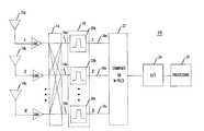
- the antenna 12 acould be a multiple frequency band antenna.
- a filter arrangement 18provides at least two different RF frequency bands on at least one channel branch 16 a-x .
- the filter arrangement 18can include a filter 20 a-x on each channel branch 16 a-x which passes a frequency band on the respective channel branch 16 a-x while attenuating other frequencies.
- the channel branch distributor 14can simply include direct connection(s) from the antenna(s) 12 a-n to the filter arrangement 18 , and the filter arrangement 18 can include a filter 20 a-x for each channel branch 16 a-x.
- a combining arrangement 22combines the RF analog signals on the channel branches 16 a-x in desired fashion.
- the resulting composite analog signalis provided with analog signals in different frequency bands to an analog to digital converter 24 which digitizes the RF analog signals and provides the digitized signals to digital processing circuitry 26 .
- the combining arrangement 22is simply a connection from the antenna 12 through the filter 20 (if required) to the A/D converter 24 .
- a sampling rate for the A/D converter 24is selected such that the frequency bands of the RF analog signals on the channel branches 16 a-x fold back to non-overlapping portions of the first Nyquist zone which reflects the Nyquist bandwidth provided by the analog to digital (A/D) converter 24 .
- the Nyquist sampling rate for a modulated analog signalfor example where an information signal is modulated onto a carrier signal, can be defined as being at least twice the highest frequency component of the information signal regardless of the carrier frequency on which the information signal is modulated.
- the informationwhich can be voice, data, video, text and/or other information, is carried in the signal bandwidth.
- the highest frequency component of the information signalis directly related to the signal bandwidth. Because the signal bandwidth is sampled at at least twice the highest frequency component of the information signal, the information signal can be reproduced in the digital domain.
- the signal bandwidthrotates or folds periodically about itself at frequency multiples or intervals (“Nyquist zones”) of one-half the sampling frequency back to a first Nyquist zone in the digital domain from 0 Hz to one-half the sampling rate.
- Nyquist zonesfrequency multiples or intervals
- a signal bandwidth and a mirror image of the signal bandwidthperiodically repeats at frequency intervals corresponding to the sampling rate of the A/D converter.
- a signal bandwidth in an odd-numbered Nyquist zonewill appear in the same relative position in odd numbered Nyquist zones back to the first Nyquist zone yet appear as a mirror image in the even-numbered Nyquist zones.
- a signal bandwidth in an even-numbered Nyquist zoneappears as a mirror image in the odd-numbered Nyquist zones back to the first Nyquist zone while appearing in the same relative position in the even-numbered Nyquist zones. Therefore, replicas of the signal bandwidth(s) are repeated at intervals of one-half the sampling rate.
- the sampling rate for the A/D converteris chosen such that after the analog signals are digitized, the desired replica frequency bands occupy non-overlapping portions or channels of the first Nyquist zone.
- the digital conversioneffectively preserves the information being produced at a rate of less than or equal to one-half the sampling rate in the bandwidth of the first Nyquist zone. If the sampling rate is increased, the first Nyquist zone or Nyquist bandwidth becomes wider.
- a fast Fourier transform (FFT) of the digital signal valuesprovides signals at frequency bands (“Nyquist zone channels”) within one-half the sampling rate (“the first Nyquist zone”) representing the converted analog signals. If the waveform is sampled at a rate less than twice its signal bandwidth (the Nyquist bandwidth), an undesirable overlapping between the adjacent periodic spectrums can occur—a well known phenomena known as aliasing. Accordingly, the sampling rate is chosen to avoid loss of information due to aliasing.
- the A/D converter 24processes the composite analog signal into Nyquist zone channels 30 a-x or bands in the first Nyquist zone.
- the Nyquist zone channels 30 a-x in the digital domaincorrespond to the different frequency bands 28 a-x of the RF analog signals.
- the digital signal processing circuitry 26can retrieve the digital signals from the Nyquist zone channels of the first Nyquist zone, because the different channels eventually end up in the first Nyquist zone after digitizing the analog input signals, for example using digital filters, digital combiners, digital detectors, digital demodulators, digital downconverters, such as a Digital Down Converter (DDC) with Numerical Controller Oscillator (NCO) to digitally down convert the data rate (which is referred to as decimation), and/or other digital processing.
- DDCDigital Down Converter
- NCONumerical Controller Oscillator
- the DDCcan tune to the respective frequencies for further signal processing. Therefore, the receiver 10 can use the bandwidth available in a single A/D to process the RF analog signals from different RF frequency bands.
- the receiver 10eliminates the need for a mixer/LO combination on any of the channel branches 16 a-x .
- a receiver 10 without a mixer/LO combinationhas many advantages. For example, without a fixed local oscillator (LO) in the frequency conversion stages, DC power consumption is reduced, re-radiation of LO out of the antenna is eliminated which reduces the need for extra front-end filtering, filter requirements at the IF are eliminated, and no image band filters are required. Because a mixer is not required, spurious mixer products as well as intermodulation distortion produced by the mixer are removed, thereby improving the spurious free dynamic range. Additionally, losses introduced by the mixer are removed which reduce the required channel gain and which improve the noise figure and the gain linearity. Furthermore, by using a single A/D converter, the receiver provides time and/or phase coherent sampling of analog signals in different frequency band(s). Different applications or signal processing schemes can benefit from such improved time and/or phase coherent measurements.
- FIG. 3shows an embodiment of a multiple band receiver 50 according to certain principles of the present invention which is used to receive communications signals in the cellular and the Personal Communications System (PCS) frequency bands.
- a base station for a “A” band cellular service providerreceives frequency channels within the A (825-835 MHz), A′′ (824-825 MHz) and A′ (845-846.5 MHz) bands.
- a base station for a B band cellular service provideruses the B (835-845 MHz) and B′ (846.5-849 MHz) frequency bands.
- a first antenna 12 areceives the modulated analog signals within the entire cellular base station receive band (824-849 MHz), and a second antenna 12 b receives the modulated analog signals in the entire PCS base station receive band (1850-1910 MHz).
- the RF analog signals from the antenna 12 aare provided to a first channel branch 16 a
- the RF analog signals from the antenna 12 bare provided to a second channel branch 16 b
- a bandpass filter 20 a on the first channel branch 16 apasses the frequencies in the cellular band (824-849 MHz) and attenuates all other frequencies.
- a bandpass filter 20 b on the second channel branch 16 bpasses the frequencies in the PCS band (1850-1910 MHz) and attenuates all other frequencies.
- LNAslow noise amplifiers
- a combining arrangement 56receives the analog signals on the first and second channel branches 16 a-b and provides the combined analog signals of the two different frequency bands to the A/D converter 24 .
- the combining arrangement 56can be a power combiner or a multiplexer filter.
- the total bandwidth of the RF analog signals on the different branches 16 a-bis 85 MHz after adding the cellular (25 MHz) and the PCS (60 MHz) bands.
- a sampling rate for the A/D converter 24is used such that the Nyquist bandwidth is sufficient to handle the 85 MHz bandwidth of the RF analog signals.
- the sampling rate for the A/D converter 24is selected such that the different frequency bands are replicated in non-overlapping portions of the Nyquist bandwidth. As such, the relative positioning of the different frequency bands within the respective Nyquist zone effects the choice of the sampling rate.
- a 400 MHz sampling rate400 Mega Samples per second
- a sampling rate400 Mega Samples per second
- a different sampling ratemay be selected to provide a different bandwidth or guard bands between the signals of the different frequency bands or branches.
- the A/D converter 24samples the combined or composite analog signals in the cellular band (824-849 MHz) and in the PCS band (1850-1910 MHz).
- the A/D converter 24produces for the digital processing circuitry 26 converted signals in a Nyquist zone channel at 24-49 MHz corresponding to the signal bandwidth in the cellular band and converted signals in a Nyquist zone channel at 90-150 MHz corresponding to the signal bandwidth in the PCS band.
- FIG. 4shows the frequency spectrum produced by the A/D converter 24 where Nyquist zones 60 a-j are repeated across the frequency spectrum at intervals of the Nyquist bandwidth or 200 MHz.
- the cellular bandappears in the fifth Nyquist zone 60 e at the A/D input frequencies of 824-849 MHz which are the RF frequencies.
- a replica of the cellular bandappears in each of the Nyquist zones back to the first Nyquist zone 60 a which provides recovery of the information signal of the cellular band at a Nyquist zone channel between 24 and 49 MHz.
- the PCS bandappears in the tenth Nyquist zone 60 j at the A/D input frequencies of 1850-1910 MHz which are the RF frequencies.
- a replica of the PCS bandappears in each of the Nyquist zones back to the first Nyquist zone 60 a which provides recovery of the information signal of the PCS band at a Nyquist zone channel between 90 and 150 MHz corresponding to a mirror image of the 1850-1910 MHz A/D input frequencies.
- the receivercan increase the utilization of the potential Nyquist bandwidth provided by the A/D converter 24 to receive RF analog signals in different frequency bands separated by large frequency differences.
- the entire cellular and PCS bandswere received and digitally converted using a single A/D converter using a sampling rate of 400 MHz.
- the A/D converterprovides replicas or images of the RF frequency bands in the first Nyquist zone which are available for digital signal processing.
- different sampling ratescan be used to increase or decrease the Nyquist bandwidth, for example to provide extra bandwidth or guard bands between the signals of the different frequency bands.
- FIG. 5shows a Nyquist zone frequency plan for an A/D converter using a sampling rate of 61.44 MHz which provides Nyquist zones which are 30.72 MHz wide.
- the Nyquist zonesare shown as 15 MHz bandwidths within each Nyquist zone as being in-band.
- FIG. 6shows a first Nyquist zone that is 30.72 MHz wide in which replicas of signals in different frequency bands at higher Nyquist zones are shown in non-overlapping portions or channels of the first Nyquist zone.
- a first Nyquist zone channel 80is shown at about 7.5 MHz with a replica of an amplitude modulated (AM) analog signal folded back from Nyquist zone 12 at 361 MHz with a 400 kHz bandwidth.
- AMamplitude modulated
- a second Nyquist zone channel 82is shown about 10 MHz with a replica of a code division multiple access (CDMA) signal folded back from Nyquist zone 61 at 1853 MHz with a 2 MHz bandwidth.
- a third Nyquist zone channel 84is shown at about 18.75 MHz with a replica of a continuous wave (CW) single tone signal folded back from Nyquist zone 5 at 141.7 MHz.
- a fourth Nyquist zone channel 86is shown at about 22 MHz with a replica of a frequency modulated (FM) signal folded back from Nyquist zone 17 at 513.5 MHz with a 4 MHz bandwidth.
- FMfrequency modulated
- the receiver according to the principles of the present inventioncan receive and digitally convert analog signals from systems using different, the same or no multiple access techniques, using the same and/or different modulation techniques, and/or using different and/or contiguous frequency bands or schemes in a single A/D converter without frequency conversion of the RF frequency bands.
- the analog signalscan be characterized as wideband, broadband and/or narrowband.
- an AM broadcast radio frequency band(550-1600 kHz) can be received by an antenna 76 and added to the combined or composite analog signal, and the A/D converter 24 could digitize the analog signals in the AM radio frequency band.
- the AM radio frequency bandwould be located in the kilohertz range of the first Nyquist zone.
- the receiver according to the principles of the present inventioncould receive signals from different sources, such as the base stations for cellular or PCS systems, AM or FM broadcast radio stations and/or GPS satellites.
- an embodiment of the receiver systemcan be used to receive signals from a North American TDMA system, a Global System For Mobile Communication (GSM) system, a code division multiple access (CDMA) system, frequency division multiple access (FDMA) systems, Global Positioning System (GPS), FM radio and/or AM radio.
- GSMGlobal System For Mobile Communication
- CDMAcode division multiple access
- FDMAfrequency division multiple access
- GPSGlobal Positioning System
- AM radioAM radio
- the embodiments of the receiver according to the principles of the present inventionhave been described with frequency band(s) associated with base station receive frequencies, but the receiver architecture according to the principles of the present invention can be used in wireless units, such as mobile units, receiving information from other frequency band(s), such as a base station transmit band which is a mobile unit receive band.
- the receiver systemhas been described using particular configurations of distinct components, but it should be understood that the receiver system and portions thereof can be implemented in application specific integrated circuits, software-driven processing circuitry, firmware, programmable logic devices, hardware or other arrangements of discrete components as would be understood by one of ordinary skill in the art with the benefit of this disclosure.
- the measurement radio architecturecan use different components which together perform similar functions when compared to the circuitry shown. What has been described is merely illustrative of the application of the principles of the present invention. Those skilled in the art will readily recognize that these and various other modifications, arrangements and methods can be made to the present invention without strictly following the exemplary applications illustrated and described herein and without departing from the spirit and scope of the present invention.
Landscapes
- Engineering & Computer Science (AREA)
- Computer Networks & Wireless Communication (AREA)
- Signal Processing (AREA)
- Superheterodyne Receivers (AREA)
- Analogue/Digital Conversion (AREA)
- Digital Transmission Methods That Use Modulated Carrier Waves (AREA)
- Circuits Of Receivers In General (AREA)
- Mobile Radio Communication Systems (AREA)
- Radio Transmission System (AREA)
Abstract
Description
Claims (20)
Priority Applications (9)
| Application Number | Priority Date | Filing Date | Title |
|---|---|---|---|
| US09/548,995US6678512B1 (en) | 2000-04-14 | 2000-04-14 | Receiver system using analog to digital conversion at radio frequency and method |
| EP00309813AEP1148653B1 (en) | 2000-04-14 | 2000-11-06 | Receiver system using analog to digital conversion at radio frequency and method |
| DE60000503TDE60000503T2 (en) | 2000-04-14 | 2000-11-06 | Receiver system with analog-digital conversion to HF and method |
| CA002337714ACA2337714C (en) | 2000-04-14 | 2001-02-22 | Receiver system using analog to digital conversion at radio frequency and method |
| BRPI0101297ABRPI0101297B1 (en) | 2000-04-14 | 2001-04-03 | receiver system using analog to digital to radio frequency conversion and method |
| AU35082/01AAU3508201A (en) | 2000-04-14 | 2001-04-10 | Receiver system using analog to digital conversion at radio frequency and method |
| CN01116523ACN1318957A (en) | 2000-04-14 | 2001-04-11 | Receiver system and method using RF analog-digital conversion |
| JP2001114703AJP3614790B2 (en) | 2000-04-14 | 2001-04-13 | Receiver system and method using analog to digital conversion at radio frequencies |
| KR10-2001-0019758AKR100539846B1 (en) | 2000-04-14 | 2001-04-13 | Receiver system using analog to digital conversion at radio frequency and method |
Applications Claiming Priority (1)
| Application Number | Priority Date | Filing Date | Title |
|---|---|---|---|
| US09/548,995US6678512B1 (en) | 2000-04-14 | 2000-04-14 | Receiver system using analog to digital conversion at radio frequency and method |
Publications (1)
| Publication Number | Publication Date |
|---|---|
| US6678512B1true US6678512B1 (en) | 2004-01-13 |
Family
ID=24191226
Family Applications (1)
| Application Number | Title | Priority Date | Filing Date |
|---|---|---|---|
| US09/548,995Expired - LifetimeUS6678512B1 (en) | 2000-04-14 | 2000-04-14 | Receiver system using analog to digital conversion at radio frequency and method |
Country Status (9)
| Country | Link |
|---|---|
| US (1) | US6678512B1 (en) |
| EP (1) | EP1148653B1 (en) |
| JP (1) | JP3614790B2 (en) |
| KR (1) | KR100539846B1 (en) |
| CN (1) | CN1318957A (en) |
| AU (1) | AU3508201A (en) |
| BR (1) | BRPI0101297B1 (en) |
| CA (1) | CA2337714C (en) |
| DE (1) | DE60000503T2 (en) |
Cited By (39)
| Publication number | Priority date | Publication date | Assignee | Title |
|---|---|---|---|---|
| US20020193090A1 (en)* | 2001-05-23 | 2002-12-19 | Sugar Gary L. | System and method for dynamic sampling rate adjustment to minimize power consumption in wideband radios |
| US20040209590A1 (en)* | 2003-04-16 | 2004-10-21 | Tim Forrester | N-plexer systems and methods for use in a wireless communications device |
| US20040217852A1 (en)* | 2000-04-24 | 2004-11-04 | Kolls H. Brock | Method for characterizing a vehicle's fuel efficiency |
| US6895310B1 (en)* | 2000-04-24 | 2005-05-17 | Usa Technologies, Inc. | Vehicle related wireless scientific instrumentation telematics |
| US20050164701A1 (en)* | 2000-08-02 | 2005-07-28 | Karabinis Peter D. | Integrated or autonomous system and method of satellite-terrestrial frequency reuse using signal attenuation and/or blockage, dynamic assignment of frequencies and/or hysteresis |
| US20050191967A1 (en)* | 2001-07-03 | 2005-09-01 | Forrester Timothy D. | System and method for a GPS enabled antenna |
| US20050233765A1 (en)* | 2004-04-16 | 2005-10-20 | Sanders Stuart B | Low cost method for receiving broadcast channels with a cellular terminal |
| US20060121862A1 (en)* | 2004-12-03 | 2006-06-08 | Cornwall Mark K | Dual mode AM-FM receiver with I-Q decoding, such as for utility data collection |
| US20060141959A1 (en)* | 2004-12-28 | 2006-06-29 | Seikaku Technical Group Limited | Multi-antenna receiving and processing circuit assembly |
| US20060227898A1 (en)* | 2003-07-10 | 2006-10-12 | Gibson Timothy P | Radio receiver |
| US20070010225A1 (en)* | 2002-04-26 | 2007-01-11 | Hirotaka Oosawa | Communication semiconductor integrated circuit device and wireless communication system |
| US20070021081A1 (en)* | 2003-04-04 | 2007-01-25 | Jens Passoke | Receiver unit and method for receiving an analogue received signal |
| US20070066254A1 (en)* | 2005-09-16 | 2007-03-22 | Kabushiki Kaisha Toshiba | Analog signal processing circuit and communication device therewith |
| US7274326B2 (en)* | 2005-02-24 | 2007-09-25 | Honeywell International Inc. | System for digital multi-bandwidth intermediate frequency processing and tracking |
| US20080084861A1 (en)* | 2006-10-10 | 2008-04-10 | Honeywell International Inc. | Avionics communication system and method utilizing multi-channel radio technology and a shared data bus |
| US20080248770A1 (en)* | 2007-04-05 | 2008-10-09 | Schultz Micha | Broadband reception system |
| US20080298519A1 (en)* | 2005-11-21 | 2008-12-04 | Fujitsu Ten Limited | Receiver Device |
| US20090017777A1 (en)* | 2007-07-13 | 2009-01-15 | Honeywell International Inc. | Reconfigurable aircraft radio communications system |
| US7502672B1 (en) | 2000-04-24 | 2009-03-10 | Usa Technologies, Inc. | Wireless vehicle diagnostics with service and part determination capabilities |
| US20090258640A1 (en)* | 2008-04-11 | 2009-10-15 | Telefonaktiebolaget Lm Ericsson | Device power detector |
| US20090298451A1 (en)* | 2008-05-29 | 2009-12-03 | Honeywell International Inc. | Reconfigurable aircraft communications system with integrated avionics communication router and audio management functions |
| US20100097966A1 (en)* | 2008-10-17 | 2010-04-22 | Hon Hai Precision Industry Co., Ltd. | Concurrent dual-band receiver and communication device having same |
| WO2010050960A1 (en)* | 2008-10-30 | 2010-05-06 | Hewlett-Packard Development Company, L.P. | Wireless device with selectable antennas |
| US20100189208A1 (en)* | 2008-12-18 | 2010-07-29 | Fudge Gerald L | System and method for clock jitter compensation in direct RF receiver architectures |
| US20100259433A1 (en)* | 2007-05-10 | 2010-10-14 | Astrium Limited | Signal Processing System |
| US20110051555A1 (en)* | 2009-09-01 | 2011-03-03 | Mitchell James B | System and Method for Determining Location of Submerged Submersible Vehicle |
| US20110075048A1 (en)* | 2009-09-30 | 2011-03-31 | Wi-Lan Inc. | Radio frequency front end for television band receiver and spectrum sensor |
| US20130023219A1 (en)* | 2010-01-19 | 2013-01-24 | Yunxin Li | Estimation of signal to noise ratio in receivers |
| US20140050212A1 (en)* | 2012-08-15 | 2014-02-20 | Andrew Llc | Telecommunication System Using Multiple Nyquist Zone Operations |
| US8711993B2 (en) | 2010-12-10 | 2014-04-29 | Honeywell International Inc. | Wideband multi-channel receiver with fixed-frequency notch filter for interference rejection |
| US20140128015A1 (en)* | 2004-01-20 | 2014-05-08 | Broadcom Corporation | Direct Digital Conversion Tuner |
| US8976302B2 (en) | 2009-09-30 | 2015-03-10 | Wi-Lan, Inc. | Radio frequency front end for television band receiver and spectrum sensor |
| US10069568B1 (en) | 2017-03-02 | 2018-09-04 | Harris Corporation | Communications system providing photonic conversion and power detection and related methods |
| US10277346B1 (en)* | 2015-07-10 | 2019-04-30 | The United States Of America As Represented By The Administrator Of National Aeronautics And Space Administration | High-efficiency secondary signal combiner |
| WO2020058980A1 (en)* | 2018-09-17 | 2020-03-26 | Elbit System Bmd And Land Ew - Elisra Ltd. | Systems and method for reducing spurious signals in a received signal |
| US11038728B1 (en)* | 2020-10-01 | 2021-06-15 | Honeywell International Inc. | Demodulating surveillance signals |
| US11251832B2 (en) | 2020-03-02 | 2022-02-15 | L-3 Communications Integrated Systems L.P. | Multiple clock sampling for Nyquist folded sampling receivers |
| US11258469B1 (en) | 2020-10-01 | 2022-02-22 | Honeywell International Inc. | Demodulating surveillance signals |
| US11356309B2 (en) | 2020-10-01 | 2022-06-07 | Honeywell International Inc. | Demodulating surveillance signals |
Families Citing this family (15)
| Publication number | Priority date | Publication date | Assignee | Title |
|---|---|---|---|---|
| US7570189B2 (en)* | 2002-06-27 | 2009-08-04 | Nxp B.V. | Radio frequency data capture |
| US7382840B2 (en)* | 2003-07-29 | 2008-06-03 | Mitsubishi Electric Research Laboratories, Inc. | RF signal processing in multi-antenna systems |
| JP2008527885A (en)* | 2005-01-13 | 2008-07-24 | エヌエックスピー ビー ヴィ | Low intermediate frequency receiver and sampling method thereof |
| US7502625B2 (en)* | 2005-01-20 | 2009-03-10 | Skyworks Solutions, Inc. | Integrated multi-band transceiver for use in mobile communication device |
| JP4662480B2 (en)* | 2006-06-10 | 2011-03-30 | Kddi株式会社 | Method and program for determining sampling frequency in undersampling |
| US7692570B2 (en)* | 2008-01-16 | 2010-04-06 | Lockheed Martin Corporation | Direct RF complex analog to digital converter |
| DE102009028919A1 (en) | 2009-08-27 | 2011-03-03 | Robert Bosch Gmbh | Method and controller for direct sampling of a plurality of radio bands |
| CN102377432B (en)* | 2010-08-27 | 2015-01-07 | 国民技术股份有限公司 | Multiplex analog-to-digital conversion device |
| EP3522467B1 (en) | 2010-10-19 | 2024-07-03 | CommScope Technologies LLC | Systems and methods for transporting digital rf signals |
| US9184771B2 (en)* | 2011-10-12 | 2015-11-10 | Optis Cellular Technology, Llc | Digital down conversion and demodulation |
| CN103580719A (en)* | 2012-08-06 | 2014-02-12 | 上海航天测控通信研究所 | Full-digital intermediate-frequency despreading demodulation receiver |
| WO2014036984A1 (en) | 2012-09-06 | 2014-03-13 | Eads Deutschland Gmbh | Radar receiver and method for receiving receive signals in a radar receiver |
| CN103684492A (en)* | 2012-09-24 | 2014-03-26 | 中兴通讯股份有限公司 | Radio frequency signal sampling device, a reception machine and a base station. |
| JP2018174415A (en)* | 2017-03-31 | 2018-11-08 | 国立大学法人東北大学 | Multiband reception apparatus and reception method of multiband high-frequency signal |
| JP2020072411A (en)* | 2018-10-31 | 2020-05-07 | アイコム株式会社 | Ad conversion device and electronic equipment |
Citations (8)
| Publication number | Priority date | Publication date | Assignee | Title |
|---|---|---|---|---|
| US5280636A (en)* | 1991-06-13 | 1994-01-18 | Hughes Aircraft Company | Multi-band digital receiving apparatus and method with bandwidth reduction |
| US5570352A (en)* | 1992-05-06 | 1996-10-29 | Nokia Telecommunications Oy | Digital cellular network/system with mobile stations communicating with base stations using frequency-hopping and having enhanced effect of interference diversity |
| US5602847A (en)* | 1995-09-27 | 1997-02-11 | Lucent Technologies Inc. | Segregated spectrum RF downconverter for digitization systems |
| WO1997005705A1 (en) | 1995-07-26 | 1997-02-13 | Telefonaktiebolaget Lm Ericsson (Publ) | Amps a-band single superhet |
| US5697078A (en)* | 1994-03-25 | 1997-12-09 | Steinbrecher Corporation | Wideband channel sniffer for monitoring channel use in a wireless communication system |
| US5995556A (en)* | 1990-06-06 | 1999-11-30 | California Institute Of Technology | Front end for GPS receivers |
| GB2338853A (en) | 1998-06-18 | 1999-12-29 | Ericsson Telefon Ab L M | Double band superheterodyne receiver with single A/D converter |
| US6195400B1 (en)* | 1997-10-20 | 2001-02-27 | Fujitsu Limited | Two-mode demodulating apparatus |
- 2000
- 2000-04-14USUS09/548,995patent/US6678512B1/ennot_activeExpired - Lifetime
- 2000-11-06EPEP00309813Apatent/EP1148653B1/ennot_activeExpired - Lifetime
- 2000-11-06DEDE60000503Tpatent/DE60000503T2/ennot_activeExpired - Lifetime
- 2001
- 2001-02-22CACA002337714Apatent/CA2337714C/ennot_activeExpired - Lifetime
- 2001-04-03BRBRPI0101297Apatent/BRPI0101297B1/ennot_activeIP Right Cessation
- 2001-04-10AUAU35082/01Apatent/AU3508201A/ennot_activeAbandoned
- 2001-04-11CNCN01116523Apatent/CN1318957A/enactivePending
- 2001-04-13JPJP2001114703Apatent/JP3614790B2/ennot_activeExpired - Lifetime
- 2001-04-13KRKR10-2001-0019758Apatent/KR100539846B1/ennot_activeExpired - Lifetime
Patent Citations (8)
| Publication number | Priority date | Publication date | Assignee | Title |
|---|---|---|---|---|
| US5995556A (en)* | 1990-06-06 | 1999-11-30 | California Institute Of Technology | Front end for GPS receivers |
| US5280636A (en)* | 1991-06-13 | 1994-01-18 | Hughes Aircraft Company | Multi-band digital receiving apparatus and method with bandwidth reduction |
| US5570352A (en)* | 1992-05-06 | 1996-10-29 | Nokia Telecommunications Oy | Digital cellular network/system with mobile stations communicating with base stations using frequency-hopping and having enhanced effect of interference diversity |
| US5697078A (en)* | 1994-03-25 | 1997-12-09 | Steinbrecher Corporation | Wideband channel sniffer for monitoring channel use in a wireless communication system |
| WO1997005705A1 (en) | 1995-07-26 | 1997-02-13 | Telefonaktiebolaget Lm Ericsson (Publ) | Amps a-band single superhet |
| US5602847A (en)* | 1995-09-27 | 1997-02-11 | Lucent Technologies Inc. | Segregated spectrum RF downconverter for digitization systems |
| US6195400B1 (en)* | 1997-10-20 | 2001-02-27 | Fujitsu Limited | Two-mode demodulating apparatus |
| GB2338853A (en) | 1998-06-18 | 1999-12-29 | Ericsson Telefon Ab L M | Double band superheterodyne receiver with single A/D converter |
Non-Patent Citations (3)
| Title |
|---|
| "12-Bit, 65 MSPS IF Sampling A/D converter", Analog Devices, Norwood, MA, pp. 1-24 (1998). |
| "CLC5526, CLC5956, and CLC5902 Diversity Receiver Chipset", National Semiconductor Corporation, Rev. 1.4, pp. 1-4 (Oct. 30, 1998). |
| "The Design of Flexible Receivers for Communicating Appliances", by Lawton, M.C. et al., IEEE, 7803-3157 pp. 1060-1064 (1996). |
Cited By (63)
| Publication number | Priority date | Publication date | Assignee | Title |
|---|---|---|---|---|
| US20040217852A1 (en)* | 2000-04-24 | 2004-11-04 | Kolls H. Brock | Method for characterizing a vehicle's fuel efficiency |
| US20050102074A1 (en)* | 2000-04-24 | 2005-05-12 | Kolls H. B. | System for interfacing with an on-board engine control system in a vehicle |
| US6895310B1 (en)* | 2000-04-24 | 2005-05-17 | Usa Technologies, Inc. | Vehicle related wireless scientific instrumentation telematics |
| US7502672B1 (en) | 2000-04-24 | 2009-03-10 | Usa Technologies, Inc. | Wireless vehicle diagnostics with service and part determination capabilities |
| US20070021060A1 (en)* | 2000-08-02 | 2007-01-25 | Atc Technologies, Llc | Integrated or autonomous system and method of satellite-terrestrial frequency reuse using signal attenuation and/or blockage, dynamic assignment of frequencies and/or hysteresis |
| US7907893B2 (en)* | 2000-08-02 | 2011-03-15 | Atc Technologies, Llc | Integrated or autonomous system and method of satellite-terrestrial frequency reuse using signal attenuation and/or blockage, dynamic assignment of frequencies and/or hysteresis |
| US20050164701A1 (en)* | 2000-08-02 | 2005-07-28 | Karabinis Peter D. | Integrated or autonomous system and method of satellite-terrestrial frequency reuse using signal attenuation and/or blockage, dynamic assignment of frequencies and/or hysteresis |
| US7831251B2 (en)* | 2000-08-02 | 2010-11-09 | Atc Technologies, Llc | Integrated or autonomous system and method of satellite-terrestrial frequency reuse using signal attenuation and/or blockage, dynamic assignment of frequencies and/or hysteresis |
| US20020193090A1 (en)* | 2001-05-23 | 2002-12-19 | Sugar Gary L. | System and method for dynamic sampling rate adjustment to minimize power consumption in wideband radios |
| US20050191967A1 (en)* | 2001-07-03 | 2005-09-01 | Forrester Timothy D. | System and method for a GPS enabled antenna |
| US7542727B2 (en) | 2001-07-03 | 2009-06-02 | Kyocera Wireless Corp. | Method for receiving a signal on a single multi-band antenna |
| US20070281651A1 (en)* | 2002-04-26 | 2007-12-06 | Hirotaka Oosawa | Communication semiconductor integrated circuit device and wireless communication system |
| US7242916B2 (en)* | 2002-04-26 | 2007-07-10 | Renesas Technology Corp. | Communication semiconductor integrated circuit device and wireless communication system |
| US20070010225A1 (en)* | 2002-04-26 | 2007-01-11 | Hirotaka Oosawa | Communication semiconductor integrated circuit device and wireless communication system |
| US20070021081A1 (en)* | 2003-04-04 | 2007-01-25 | Jens Passoke | Receiver unit and method for receiving an analogue received signal |
| US20040209590A1 (en)* | 2003-04-16 | 2004-10-21 | Tim Forrester | N-plexer systems and methods for use in a wireless communications device |
| US7376440B2 (en)* | 2003-04-16 | 2008-05-20 | Kyocera Wireless Corp. | N-plexer systems and methods for use in a wireless communications device |
| US20060227898A1 (en)* | 2003-07-10 | 2006-10-12 | Gibson Timothy P | Radio receiver |
| US20070275679A1 (en)* | 2003-07-10 | 2007-11-29 | Gibson Timothy P | Radio receiver for aviation communications and navigation |
| US20140128015A1 (en)* | 2004-01-20 | 2014-05-08 | Broadcom Corporation | Direct Digital Conversion Tuner |
| US20050233765A1 (en)* | 2004-04-16 | 2005-10-20 | Sanders Stuart B | Low cost method for receiving broadcast channels with a cellular terminal |
| US8000675B2 (en)* | 2004-04-16 | 2011-08-16 | Sony Ericsson Mobile Communications Ab | Low cost method for receiving broadcast channels with a cellular terminal |
| US20060121862A1 (en)* | 2004-12-03 | 2006-06-08 | Cornwall Mark K | Dual mode AM-FM receiver with I-Q decoding, such as for utility data collection |
| US7400904B2 (en)* | 2004-12-03 | 2008-07-15 | Itron, Inc. | Dual mode AM-FM receiver with I-Q decoding, such as for utility data collection |
| US7400871B2 (en)* | 2004-12-28 | 2008-07-15 | Seikaku Technical Group Limited | Multi-antenna receiving and processing circuit assembly |
| US20060141959A1 (en)* | 2004-12-28 | 2006-06-29 | Seikaku Technical Group Limited | Multi-antenna receiving and processing circuit assembly |
| US7274326B2 (en)* | 2005-02-24 | 2007-09-25 | Honeywell International Inc. | System for digital multi-bandwidth intermediate frequency processing and tracking |
| US20070066254A1 (en)* | 2005-09-16 | 2007-03-22 | Kabushiki Kaisha Toshiba | Analog signal processing circuit and communication device therewith |
| US20080298519A1 (en)* | 2005-11-21 | 2008-12-04 | Fujitsu Ten Limited | Receiver Device |
| US20080084861A1 (en)* | 2006-10-10 | 2008-04-10 | Honeywell International Inc. | Avionics communication system and method utilizing multi-channel radio technology and a shared data bus |
| US20080248770A1 (en)* | 2007-04-05 | 2008-10-09 | Schultz Micha | Broadband reception system |
| US20100259433A1 (en)* | 2007-05-10 | 2010-10-14 | Astrium Limited | Signal Processing System |
| US8081933B2 (en) | 2007-07-13 | 2011-12-20 | Honeywell International Inc. | Reconfigurable aircraft radio communications system |
| US20090017777A1 (en)* | 2007-07-13 | 2009-01-15 | Honeywell International Inc. | Reconfigurable aircraft radio communications system |
| US20090258640A1 (en)* | 2008-04-11 | 2009-10-15 | Telefonaktiebolaget Lm Ericsson | Device power detector |
| US20090298451A1 (en)* | 2008-05-29 | 2009-12-03 | Honeywell International Inc. | Reconfigurable aircraft communications system with integrated avionics communication router and audio management functions |
| US8019338B2 (en) | 2008-05-29 | 2011-09-13 | Honeywell International Inc. | Reconfigurable aircraft communications system with integrated avionics communication router and audio management functions |
| US8736380B2 (en) | 2008-10-10 | 2014-05-27 | The Johns Hopkins University | Amplifier for buoyant cable antenna |
| US20100097966A1 (en)* | 2008-10-17 | 2010-04-22 | Hon Hai Precision Industry Co., Ltd. | Concurrent dual-band receiver and communication device having same |
| US20110151811A1 (en)* | 2008-10-30 | 2011-06-23 | Isaac Lagnado | Wireless Device With Selectable Antennas |
| WO2010050960A1 (en)* | 2008-10-30 | 2010-05-06 | Hewlett-Packard Development Company, L.P. | Wireless device with selectable antennas |
| US8509368B2 (en) | 2008-12-18 | 2013-08-13 | L-3 Communications Integrated Systems, L.P. | System and method for clock jitter compensation in direct RF receiver architectures |
| US20100189208A1 (en)* | 2008-12-18 | 2010-07-29 | Fudge Gerald L | System and method for clock jitter compensation in direct RF receiver architectures |
| US20110051555A1 (en)* | 2009-09-01 | 2011-03-03 | Mitchell James B | System and Method for Determining Location of Submerged Submersible Vehicle |
| US8289811B2 (en) | 2009-09-01 | 2012-10-16 | The Johns Hopkins University | System and method for determining location of submerged submersible vehicle |
| US8976302B2 (en) | 2009-09-30 | 2015-03-10 | Wi-Lan, Inc. | Radio frequency front end for television band receiver and spectrum sensor |
| US20110075048A1 (en)* | 2009-09-30 | 2011-03-31 | Wi-Lan Inc. | Radio frequency front end for television band receiver and spectrum sensor |
| US8350970B2 (en)* | 2009-09-30 | 2013-01-08 | Wi-Lan, Inc. | Radio frequency front end for television band receiver and spectrum sensor |
| US20130023219A1 (en)* | 2010-01-19 | 2013-01-24 | Yunxin Li | Estimation of signal to noise ratio in receivers |
| US9143286B2 (en)* | 2010-01-19 | 2015-09-22 | Nitero Pty Limited | Estimation of signal to noise ratio in receivers |
| US9042502B2 (en) | 2010-12-10 | 2015-05-26 | Honeywell International Inc. | Wideband multi-channel receiver with fixed-frequency notch filter for interference rejection |
| US8711993B2 (en) | 2010-12-10 | 2014-04-29 | Honeywell International Inc. | Wideband multi-channel receiver with fixed-frequency notch filter for interference rejection |
| US20140050212A1 (en)* | 2012-08-15 | 2014-02-20 | Andrew Llc | Telecommunication System Using Multiple Nyquist Zone Operations |
| US9614629B2 (en)* | 2012-08-15 | 2017-04-04 | Commscope Technologies Llc | Telecommunication system using multiple Nyquist zone operations |
| US9667368B2 (en)* | 2012-08-15 | 2017-05-30 | Commscope Technologies Llc | Telecommunication system using multiple nyquist zone operations |
| US10075252B2 (en) | 2012-08-15 | 2018-09-11 | Commscope Technologies Llc | Telecommunication system using multiple Nyquist zone operations |
| US10277346B1 (en)* | 2015-07-10 | 2019-04-30 | The United States Of America As Represented By The Administrator Of National Aeronautics And Space Administration | High-efficiency secondary signal combiner |
| US10069568B1 (en) | 2017-03-02 | 2018-09-04 | Harris Corporation | Communications system providing photonic conversion and power detection and related methods |
| WO2020058980A1 (en)* | 2018-09-17 | 2020-03-26 | Elbit System Bmd And Land Ew - Elisra Ltd. | Systems and method for reducing spurious signals in a received signal |
| US11251832B2 (en) | 2020-03-02 | 2022-02-15 | L-3 Communications Integrated Systems L.P. | Multiple clock sampling for Nyquist folded sampling receivers |
| US11038728B1 (en)* | 2020-10-01 | 2021-06-15 | Honeywell International Inc. | Demodulating surveillance signals |
| US11258469B1 (en) | 2020-10-01 | 2022-02-22 | Honeywell International Inc. | Demodulating surveillance signals |
| US11356309B2 (en) | 2020-10-01 | 2022-06-07 | Honeywell International Inc. | Demodulating surveillance signals |
Also Published As
| Publication number | Publication date |
|---|---|
| AU3508201A (en) | 2001-10-18 |
| JP2002026758A (en) | 2002-01-25 |
| EP1148653A1 (en) | 2001-10-24 |
| KR100539846B1 (en) | 2005-12-28 |
| DE60000503D1 (en) | 2002-10-31 |
| EP1148653B1 (en) | 2002-09-25 |
| BR0101297A (en) | 2001-11-13 |
| BRPI0101297B1 (en) | 2015-12-29 |
| DE60000503T2 (en) | 2003-06-26 |
| CN1318957A (en) | 2001-10-24 |
| CA2337714C (en) | 2005-09-13 |
| JP3614790B2 (en) | 2005-01-26 |
| CA2337714A1 (en) | 2001-10-14 |
| KR20010098566A (en) | 2001-11-08 |
Similar Documents
| Publication | Publication Date | Title |
|---|---|---|
| US6678512B1 (en) | Receiver system using analog to digital conversion at radio frequency and method | |
| US6574459B1 (en) | Multiple branch receiver system and method | |
| US5602847A (en) | Segregated spectrum RF downconverter for digitization systems | |
| KR100671364B1 (en) | Method and system for direct conversion multicarrier processor | |
| FI114177B (en) | Digitizer and digitization method for broadband signal | |
| KR0149893B1 (en) | Method and apparatus for receiving electromagnetic radiation within a frequency band | |
| US20070066254A1 (en) | Analog signal processing circuit and communication device therewith | |
| KR20030067699A (en) | Multipath communications receiver | |
| IL214000A (en) | Efficient sampling and reconstruction of sparse multi-band signals | |
| CN107147427A (en) | A kind of method of sampling of signal, device and system | |
| CN101789922A (en) | Method and apparatus for extracting data from multiple data signals of different carrier frequencies | |
| US6944238B2 (en) | Digital transmitter system and method | |
| EP2403145A1 (en) | A receiver and a method for processing a signal | |
| KR100790858B1 (en) | Direct conversion receiver and receiving method with time-sharing I channel and Q channel | |
| KR100964383B1 (en) | Digital Intensive RF Receiver | |
| Wang et al. | A feasible rf bandpass sampling architecture of single-channel software-defined radio receiver | |
| Wang et al. | Antialiasing method for image aliasing in bandpass-sampling-based receiver | |
| Efstathiou | Base station transceiver trends for 3G and beyond wireless systems | |
| US20120155581A1 (en) | Implementation of a high performance multi-carrier receiver using frequency selectivity and digital compensation techniques |
Legal Events
| Date | Code | Title | Description |
|---|---|---|---|
| AS | Assignment | Owner name:LUCENT TECHNOLOGIES INC., NEW JERSEY Free format text:ASSIGNMENT OF ASSIGNORS INTEREST;ASSIGNORS:KAMINSKI, WALTER JOSEPH;KOLSRUD, ARILD;REEL/FRAME:010751/0645 Effective date:20000412 | |
| FEPP | Fee payment procedure | Free format text:PAYOR NUMBER ASSIGNED (ORIGINAL EVENT CODE: ASPN); ENTITY STATUS OF PATENT OWNER: LARGE ENTITY | |
| STCF | Information on status: patent grant | Free format text:PATENTED CASE | |
| FPAY | Fee payment | Year of fee payment:4 | |
| FPAY | Fee payment | Year of fee payment:8 | |
| AS | Assignment | Owner name:CREDIT SUISSE AG, NEW YORK Free format text:SECURITY INTEREST;ASSIGNOR:ALCATEL-LUCENT USA INC.;REEL/FRAME:030510/0627 Effective date:20130130 | |
| AS | Assignment | Owner name:ALCATEL-LUCENT USA INC., NEW JERSEY Free format text:RELEASE BY SECURED PARTY;ASSIGNOR:CREDIT SUISSE AG;REEL/FRAME:033950/0261 Effective date:20140819 | |
| FPAY | Fee payment | Year of fee payment:12 | |
| AS | Assignment | Owner name:ALCATEL-LUCENT USA INC., NEW JERSEY Free format text:MERGER AND CHANGE OF NAME;ASSIGNORS:LUCENT TECHNOLOGIES INC.;ALCATEL USA MARKETING, INC.;ALCATEL USA SOURCING, INC.;AND OTHERS;REEL/FRAME:046313/0453 Effective date:20081101 |