US6678085B2 - High-contrast display system with scanned conformal grating device - Google Patents
High-contrast display system with scanned conformal grating deviceDownload PDFInfo
- Publication number
- US6678085B2 US6678085B2US10/171,252US17125202AUS6678085B2US 6678085 B2US6678085 B2US 6678085B2US 17125202 AUS17125202 AUS 17125202AUS 6678085 B2US6678085 B2US 6678085B2
- Authority
- US
- United States
- Prior art keywords
- projection system
- improved projection
- linear array
- cross
- order
- Prior art date
- Legal status (The legal status is an assumption and is not a legal conclusion. Google has not performed a legal analysis and makes no representation as to the accuracy of the status listed.)
- Expired - Fee Related
Links
Images


Classifications
- H—ELECTRICITY
- H04—ELECTRIC COMMUNICATION TECHNIQUE
- H04N—PICTORIAL COMMUNICATION, e.g. TELEVISION
- H04N9/00—Details of colour television systems
- H04N9/12—Picture reproducers
- H04N9/31—Projection devices for colour picture display, e.g. using electronic spatial light modulators [ESLM]
- H04N9/3129—Projection devices for colour picture display, e.g. using electronic spatial light modulators [ESLM] scanning a light beam on the display screen
- G—PHYSICS
- G02—OPTICS
- G02B—OPTICAL ELEMENTS, SYSTEMS OR APPARATUS
- G02B26/00—Optical devices or arrangements for the control of light using movable or deformable optical elements
- G02B26/08—Optical devices or arrangements for the control of light using movable or deformable optical elements for controlling the direction of light
- G02B26/0808—Optical devices or arrangements for the control of light using movable or deformable optical elements for controlling the direction of light by means of one or more diffracting elements
Definitions
- This inventionrelates to a display system with a linear array of electromechanical grating devices that is scanned in order to generate a two-dimensional image. More particularly, the invention relates to a high-contrast laser display system containing electromechanical conformal grating devices.
- Spatial light modulators based on electromechanical grating devicesare important for a wide range of applications, including display, data storage, spectroscopy and printing. Such systems require large numbers of individually addressable devices in either a linear or area array, with over a million addressable devices desirable for an area modulator array in a high-quality display.
- an electromechanical conformal grating deviceconsisting of ribbon elements suspended above a substrate by a periodic sequence of intermediate supports was disclosed by Kowarz in U.S. Pat. No. 6,307,663, entitled “ Spatial Light Modulator With Conformal Grating Device ” issued Oct. 23, 2001.
- the electromechanical conformal grating deviceis operated by electrostatic actuation, which causes the ribbon elements to conform around the support substructure, thereby producing a grating.
- the device of '663has more recently become known as the conformal GEMS device, with GEMS standing for grating electromechanical system.
- the conformal GEMS devicepossesses a number of attractive features. It provides high-speed digital light modulation with high contrast and good efficiency.
- the active regionis relatively large and the grating period is oriented perpendicular to the array direction. This orientation of the grating period causes diffracted light beams to separate in close proximity to the linear array and to remain spatially separated throughout most of an optical system.
- an improved projection systemthat includes a conformal grating electromechanical system (GEMS) device for forming an image on a medium, and also including: a light source providing illumination; a linear array of conformal GEMS devices receiving the illumination; an obstructing element for blocking a zeroth order reflected light beam from reaching the medium; a cross-order filter placed substantially near a Fourier plane of a lens system for blocking a plurality of diffracted cross-order light beams from reaching the medium; a scanning element for moving non-obstructed diffracted light beams relative to the medium; and a controller for providing a data stream to the individually operable devices.
- GEMSconformal grating electromechanical system
- FIG. 1is a perspective, partially cut-away view of two conformal GEMS devices in a linear array
- FIG. 2is a top view of four conformal GEMS devices in a linear array
- FIGS. 3 a and 3 bare cross-sectional views through line 3 , 5 — 3 , 5 in FIG. 2, showing the operation of a conformal GEMS device in an unactuated state and an actuated state, respectively;
- FIGS. 4 a and 4 bare cross-sectional views through line 4 — 4 in FIG. 2 showing the conformal GEMS device in an unactuated state and an actuated state, respectively;
- FIG. 5 ais a cross-sectional view through line 3 , 5 — 3 , 5 in FIG. 2, showing an unactuated conformal GEMS device that contains residual ribbon curvature;
- FIG. 5 bis a cross-sectional view through line 4 — 4 in FIG. 2, showing an unactuated conformal GEMS device that contains residual ribbon curvature;
- FIG. 6is a top view of four conformal GEMS devices in a linear array, wherein each of the devices contains two ribbon elements;
- FIG. 7is a topographical representation of residual ribbon curvature in conformal GEMS devices.
- FIG. 8is a three-dimensional plot of residual ribbon curvature in a single cell of FIG. 7;
- FIG. 9is a schematic illustrating a line-scanned display system with high contrast according to the present invention.
- FIG. 10shows a linear array of conformal GEMS devices illuminated by a line of light
- FIG. 11is a view of the projection screen that illustrates the formation of a two-dimensional image by scanning a line image across the screen;
- FIGS. 12 a - 12 dare density plots of the light distribution in different planes of FIG. 9 between the linear array of conformal GEMS devices and the projection lens, wherein the devices are actuated;
- FIGS. 13 a - 13 dare density plots of the light distribution in different planes of FIG. 9 after the projection lens, wherein the conformal GEMS devices are actuated;
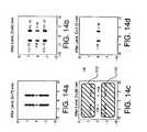
- FIGS. 14 a - 14 dare density plots of the light distribution in different planes of FIG. 9 after the projection lens, wherein the conformal GEMS devices are not actuated and the ribbons have residual curvature;
- FIG. 15is a schematic illustrating a three-color embodiment of a line-scanned display system with high contrast
- FIG. 16is a schematic illustrating a second three-color embodiment of a line-scanned display system with high contrast
- FIG. 17is a schematic illustrating a third three-color embodiment of a line-scanned display system with high contrast.
- FIG. 18illustrates the spatial filter used in the third three-color embodiment of FIG. 17 .
- FIGS. 1-3The conformal Grating Electromechanical System (GEMS) devices are illustrated in FIGS. 1-3.
- FIG. 1shows two side-by-side conformal GEMS devices 5 a and 5 b in an unactuated state.
- the conformal GEMS devices 5 a and 5 bare formed on top of a substrate 10 covered by a bottom conductive layer 12 , which acts as an electrode to actuate the devices 5 a , 5 b .
- the bottom conductive layer 12is covered by a dielectric protective layer 14 followed by a standoff layer 16 and a spacer layer 18 .
- a ribbon layer 20is formed which is covered by a reflective layer and conductive layer 22 .
- the reflective and conductive layer 22provides electrodes for the actuation of the conformal GEMS devices 5 a and 5 b . Accordingly, the reflective and conductive layer 22 is patterned to provide electrodes for the two conformal GEMS devices 5 a and 5 b .
- the ribbon layer 20preferably, comprises a material with a sufficient tensile stress to provide a large restoring force.
- Each of the two conformal GEMS devices 5 a and 5 bhas an associated elongated ribbon element 23 a and 23 b , respectively, patterned from the reflective and conductive layer 22 and the ribbon layer 20 .
- the elongated ribbon elements 23 a and 23 bare supported by end supports 24 a and 24 b , formed from the spacer layer 18 , and by one or more intermediate supports 27 that are uniformly separated in order to form equal-width channels 25 .
- the elongated ribbon elements 23 a and 23 bare secured to the end supports 24 a and 24 b and to the intermediate supports 27 .
- a plurality of square standoffs 29is patterned at the bottom of the channels 25 from the standoff layer 16 . These standoffs 29 reduce the possibility of the elongated ribbon elements 23 a and 23 b sticking when actuated.
- FIG. 2A top view of a four-device linear array of conformal GEMS devices 5 a , 5 b , 5 c and 5 d is shown in FIG. 2 .
- the elongated ribbon elements 23 a , 23 b , 23 c , and 23 dare depicted partially removed over the portion of the diagram below the line A—A in order to show the underlying structure.
- the intermediate supports 27should preferably be completely hidden below the elongated ribbon elements 23 a , 23 c , and 23 d . Therefore, when viewed from the top, the intermediate supports 27 should not be visible in the gaps 28 between the conformal GEMS devices 5 a - 5 d .
- each of the conformal GEMS devices 5 a - 5 dhas three intermediate supports 27 with four equal-width channels 25 .
- the center-to-center separation A of the intermediate supports 27defines the period of the conformal GEMS devices in the actuated state.
- the elongated ribbon elements 23 a - 23 dare mechanically and electrically isolated from one another, allowing independent operation of the four conformal GEMS devices 5 a - 5 d .
- the bottom conductive layer 12 of FIG. 1can be common to all of the conformal GEMS devices 5 a - 5 d.
- FIG. 3 ais a side view, through line 3 , 5 — 3 , 5 of FIG. 2, of two channels 25 of the conformal GEMS device 5 b (as shown and described in FIGS. 1 and 2) in an unactuated state.
- FIG. 3 bshows the same view for an actuated state.
- an attractive electrostatic forceis produced by applying a voltage difference between the bottom conductive layer 12 and the reflective and conductive layer 22 of the elongated ribbon element 23 b .
- the ribbon element 23 bis suspended flat between the supports.
- an incident light beam 30is primarily reflected into a 0th order light beam 32 , as in a simple planar mirror.
- FIG. 3 bshows the device 5 b (as shown and described in FIGS. 1 and 2) in the fully actuated state with the elongated ribbon element 23 b in contact with standoffs 29 .
- the height difference between the bottom of element 23 b and the top of the standoffs 29is chosen to be approximately 1 ⁇ 4 of the wavelength ⁇ of the incident light. The optimum height depends on the specific conformal shape of the actuated device.
- the incident light beam 30is primarily diffracted into the +1st order light beam 35 a and ⁇ 1st order light beam 35 b , with additional light diffracted into the +2nd order 36 a and ⁇ 2nd order 36 b .
- a small amount of lightis diffracted into even higher orders and some light remains in the 0th order.
- one or more of the various beamscan be collected and used by an optical system, depending on the application.
- FIGS. 4 a and 4 bshow a side view through line 4 — 4 of FIG. 2 of the conformal GEMS device 5 b in the unactuated and actuated states, respectively.
- the conductive reflective ribbon element 23 bis suspended by the end support 24 b and the adjacent intermediate support 27 (not shown in this perspective).
- the application of a voltageactuates the device as illustrated in FIG. 4 b.
- a linear array of conformal GEMS devicesis formed by arranging the devices as illustrated in FIGS. 1-2 with the direction of the grating period A perpendicular to the axis of the array.
- the planes containing the various diffracted light beamsthen intersect in a line at the linear array and are distinct away from the linear array.
- the diffracted light beamsbecome spatially separated in close proximity to the linear array. This feature simplifies the optical system design and allows for the selection of specific diffracted light beams without the use of Schlieren optics.
- the conformal GEMS devices illustrated in FIGS. 1-4would, when actuated, produce non-zero diffracted orders (+1 st order 35 a , ⁇ 1 st order 35 b , +2 nd order 36 a and ⁇ 2 nd order 36 b ) that have very high contrast.
- This ideal situationarises if, in the unactuated state, the ribbon elements 23 a , 23 b , 23 c and 23 d are suspended perfectly flat between the intermediate supports 27 and, hence, do not cause any diffraction of light into non-zero diffracted orders.
- FIGS. 5 a and 5 bwhich are similar to FIGS. 3 a and 4 a , respectively.
- FIG. 5 ais a side view, through line 3 , 5 — 3 , 5 of FIG. 2, of two channels 25 of the conformal GEMS device 5 b , with the addition of ribbon curvature.
- FIG. 5 bshows a rotated side view of the same device along the direction of the ribbon width w.
- the ribbon curvaturecauses a weak grating to be present even when the conformal GEMS device 5 b is not actuated, thus reducing system contrast.
- a contrast above 1000:1is often required. (Contrast is defined as the ratio of diffracted light intensity with the device actuated to diffracted light intensity with the device unactuated.)
- FIG. 6depicts a top view of a four-device linear array similar to FIG. 2 .
- Each of the conformal GEMS devices 5 a , 5 b , 5 c , and 5 dnow has an associated pair of subdivided elongated conductive reflective ribbon elements ( 51 a , 52 a ), ( 51 b , 52 b ), ( 51 c , 52 c ), and ( 51 d , 52 d ), respectively.
- This subdivision of each conformal GEMS device 5 a , 5 b , 5 c , and 5 dpermits fabrication of wider conformal GEMS devices, without significantly impacting optical performance.
- the preferred method of fabricationis to etch a sacrificial layer (not shown) from the channel 25 , thus releasing the elongated conductive ribbon elements ( 51 a , 52 a ), ( 51 b , 52 b ), ( 51 c , 52 c ), and ( 51 d , 52 d ).
- the subdivided gaps 55 between the elongated conductive elements ( 51 a , 52 a ), ( 51 b , 52 b ), ( 51 c , 52 c ), and ( 51 d , 52 d )allow the etchant to access this sacrificial layer. Increasing the number of subdivided gaps 55 can therefore improve the etching process.
- the conformal GEMS devices 5 a , 5 b , 5 c , and 5 dmay be necessary to further subdivide the conformal GEMS devices 5 a , 5 b , 5 c , and 5 d into more than two.
- the elongated-conductive reflective ribbon elements ( 51 a , 52 a ), ( 51 b , 52 b ), ( 51 c , 52 c ), and ( 51 d , 52 d )are depicted partially removed over the portion of the diagram below the line A—A in order to show the underlying structure.
- the intermediate supports 27should be completely hidden below the elongated-conductive reflective ribbon elements 51 a , 52 a , 51 b , 52 b , 51 c , 52 c , 51 d , and 52 d .
- the intermediate supports 27should not penetrate into the subdivided gaps 55 .
- the ribbon elements within a single conformal GEMS deviceare mechanically isolated, but electrically coupled. They therefore operate in unison when a voltage is applied.
- FIG. 7is a top view illustration of an unactuated linear array of conformal GEMS devices 5 a - 5 d , similar to FIG. 6, with a contour map overlay of the ribbon elements' surface profile showing ribbon curvature.
- Each cell 54 within the elongated-conductive ribbon elements 51 a , 52 a , 51 b , 52 b , 51 c , 52 c , 51 d , and 52 dhas a saddle-like shape, shown in more detail in the three-dimensional plot of FIG. 8 .
- cells 54form a two-dimensional periodic pattern that acts as a reflective crossed grating.
- the peak-to-peak height of the crossed gratingis less than 40 nm, i.e., less than a tenth of a wavelength for visible wavelengths.
- the period of the crossed grating along the length of the elongated-conductive reflective ribbon elements 51 a - 51 d and 52 a - 52 dis equal to the conformal GEMS period ⁇ , as determined by the placement of the intermediate supports 27 .
- the period of the crossed grating in the perpendicular directionis the ribbon period p.
- a particular conformal GEMS deviceIf a particular conformal GEMS device is actuated, it reflects the incident light beam primarily into the 0th order light beam, which is directed back towards the source 70 by the turning mirror 82 . If a particular conformal GEMS device is actuated, it diffracts the incident light beams primarily into +2 nd , +1 st , ⁇ 1 st and ⁇ 2nd order light beams. These diffracted light beams pass around the turning mirror 82 and are projected on the screen 90 by the projection lens system 75 . A cross-order filter 110 placed near the Fourier (focal) plane “f” of the projection lens system 75 prevents the undesirable diffracted cross-orders from reaching the screen 90 .
- the scanning mirror 77sweeps the line image across the screen 90 to form the two-dimensional scene.
- the controller 80provides synchronization between the sweep of the scanning mirror 77 and a data stream that provides the scene content.
- FIG. 10depicts a linear array 85 of conformal GEMS devices (P 1 . . . P 1080 ) illuminated by a line of light 88 parallel to the long axis of the linear array 85 .
- the grating period ⁇(not shown) is preferably perpendicular to the long axis of the linear array 85 and to the line of light 88 .
- FIG. 11is a view facing the screen 90 of the display system 900 , shown in FIG. 9, and depicts the formation of the two-dimensional scene.
- HDTV resolutionis obtained by scanning the image of the linear array 85 of 1080 conformal GEMS devices to generate 1920 sequential lines, thereby producing a scene with 1080 by 1920 pixels.
- FIGS. 12 a - 12 dillustrate the propagation of the diffracted light beams through the display system 900 of FIG. 9 in several planes prior to the projection lens system 75 .
- FIGS. 13 a - 13 dshow the light distribution after the projection lens system 75 .
- the light source 70is a laser
- the lenshas a focal length f of 50 mm
- the linear arrayis 1 cm long and all of the conformal GEMS devices on the linear array 85 are turned on.
- Drefers to the distance between the linear array 85 to the plane of interest.
- FIG. 12 dshows the light distribution at the turning mirror 82 , which is located close to the projection lens system 75 .
- the turning mirror 82blocks the unwanted 0 th diffracted order and reflects it back towards the source 70 .
- six diffracted orders from ⁇ 3 rd to ⁇ 1 st and +1 st to +3 rdare allowed to pass through the projection lens system 75 .
- FIGS. 13 a - 13 dshow these diffracted orders after they have gone through the projection lens system 75 .
- the diffracted ordersare tightly focused into six spots. It is, therefore, preferable to place the scanning mirror 77 close to the Fourier plane to minimize its size and weight. Eventually, as the six diffracted orders continue propagating towards the screen 90 , they again become overlapping spatially near the image plane at the screen 90 .
- FIGS. 12 a - 12 d and 13 a - 13 ddescribe light propagation through the display system 900 of FIG. 9 when all of the conformal GEMS devices of the linear array 85 are turned on. Obviously, when the conformal GEMS devices are turned off, any light that is not obstructed will reduce the contrast and quality of the image on the screen 90 .
- FIGS. 14 a - 14 dillustrate the off-state light distribution in several planes after the projection lens system 75 of FIG. 9 .
- the conformal GEMS devices modeled in FIGS. 14 a - 14 dhave ribbon curvature that produces a weak crossed grating. Some light is still present in the primary +1 st and ⁇ 1 st orders.
- the intensity of these ordersis substantially less, often by a factor of 1000 or more, than the corresponding orders in FIGS. 12 a - 12 d and 13 a - 13 d .
- the higher orders, ⁇ 3 rd , 2 nd , +2 nd and +3 rdare now reduced to the point that they are not visible in the figures.
- the crossed gratinggenerates four dominant diffracted cross-orders labeled (+1,+1), (+1, ⁇ 1), ( ⁇ 1,+1) and ( ⁇ 1, ⁇ 1) in FIGS. 14 b and 14 c . As shown in FIG.
- the cross-order filter 110by placing a cross-order filter 110 substantially near the Fourier plane of the projection lens system 75 , the aforementioned four cross-orders can be separated and blocked while leaving the desired diffracted orders unaffected.
- the cross-order filterIn order to effectively separate the diffracted cross-orders from the primary +1 st and ⁇ 1 st orders, the cross-order filter should be placed at a distance less than approximately (f 2 ⁇ )/(L ⁇ ) from the Fourier plane, where ⁇ is the wavelength and L is the length of the linear array 85 .
- the cross-order filter 110increases system contrast without substantially decreasing optical efficiency. The contrast improvement enabled by the addition of the cross-order filter 110 depends on the exact profile of the crossed grating, i.e., on the specific saddle-like shape of each cell 54 .
- the obstructing elementsare the turning mirror 82 that blocks the 0 th order light beam and the cross-order filter 110 that blocks the (+1,+1), (+1, ⁇ 1), ( ⁇ 1,+1) and ( ⁇ 1, ⁇ 1) diffracted cross-orders.
- similar obstructing elementsare used to prevent unwanted diffracted light beams from reaching the screen. As is well known to those skilled in the art, a variety of elements may be used for this purpose.
- cross-order filter 110could be an absorbing stop or a pair of tilted mirrors.
- the scanning mirror 77could be designed so that the diffracted cross-orders pass above and below the mirror edges, therefore, never becoming part of the image. This appropriately-sized scanning mirror 77 would then also function as a cross-order filter.
- the light illuminating the linear array of conformal GEMS devicesneeds to have a relatively small spread in angles of incidence.
- the conformal GEMS deviceshave a period of 30 microns and the illuminating wavelength is 532 nm, the angular separation between the 0 th order light beam and the +1 st order light beam is approximately 1 degree. Therefore, the total angular spread of the light incident upon the linear array should be less than 1 degree, in the plane perpendicular to the linear array.
- the angular spread of the incident lightshould also be sufficiently narrow in the plane parallel to the linear array.
- a coherent laseris the most optically efficient for generating light with such a narrow range of incident angles.
- incoherent sourcessuch as filament lamps and light emitting diodes, a vast majority of the optical power would be wasted by the illumination system in the process of generating the required illumination.
- the embodiment of FIG. 9can be used either for single color or for color-sequential display systems.
- the light source 70produces a plurality of colors that are sequential in time and the controller 80 is synchronized with the light source 70 .
- the controller 80is synchronized with the light source 70 .
- the light source 70consists of three combined red, green, and blue lasers, these are turned on sequentially to produce overlapping red, green, and blue images on the screen 90 .
- the image data sent by the controller 80 to the linear array 85is synchronized with the respective turned-on laser color.
- FIGS. 15, 16 , and 17depict embodiments of the invention that project three colors simultaneously, (for example, red, green, and blue).
- three separate light sources 70 r , 70 g , 70 beach with their own illumination optics 72 r , 72 g , 72 b , 74 r , 74 g , 74 b , provide light to the three linear arrays 85 r , 85 g , 85 b via three turning mirrors 82 r , 82 g , 82 b .
- Red lightilluminates linear array 85 r , green light linear array 85 g and blue light linear array 85 b .
- the ⁇ 3 rd , ⁇ 2 nd , ⁇ 1 st , +1 st , +2 nd , and +3 rd order light beams emerging from the three linear arrays 85 r , 85 g , 85 b ,are combined by a color-combining element, shown as a color-combining cube 100 in FIG. 15 .
- the 0 th order light beamsare directed towards their respective sources by the turning mirrors 82 r , 82 g , 82 b .
- a single projection lens system 75forms a three-color line image of the three linear arrays 85 r , 85 g , 85 b on the screen 90 (not shown in figure).
- the sweep of the scanning mirror 77(not shown in figure) generates a two-dimensional image from the line image.
- cross-ordersare removed by the cross-order filter 110 at the Fourier plane of the projection lens 75 .
- FIG. 16shows an alternate color-simultaneous embodiment in which the three turning mirrors 82 r , 82 g , 82 b of FIG. 15 are replaced by polarization beam splitters 114 r , 114 g , 114 b with 1 ⁇ 4 wave plates 116 r , 116 g , 116 b and 0 th order stops 118 r , 118 g , 118 b .
- the combination of polarization beam splitter, 1 ⁇ 4 wave plate and 0 th order stopprovides easier alignment tolerances than when the illumination and obstruction functions are combined, as in the turning mirror solution.
- the system of FIG. 16contains three separate projection lenses 75 r , 75 g , 75 b.
- FIG. 17shows a variation of the system in FIG. 16 in which a single spatial filter 111 placed at the Fourier plane of the projection lenses 75 r , 75 g , 75 b replaces the three 0 th order stops 118 r , 118 g , 118 b and the cross-order filter 110 .
- the spatial filter 111has a 0 th order portion 111 b to block 0 th order light beams and a cross-order portion 111 a to block cross-orders.
- the same principlescan be used to implement high-contrast printing systems based on linear arrays of conformal GEMS devices.
- the image mediumwould be a light reactive material, such as photographic paper, thermally activated media, or thermal transfer media.
- the scanning mirror 77would typically be replaced by a paper transport system that serves as the scanning element.
Landscapes
- Physics & Mathematics (AREA)
- Optics & Photonics (AREA)
- Engineering & Computer Science (AREA)
- Multimedia (AREA)
- Signal Processing (AREA)
- General Physics & Mathematics (AREA)
- Mechanical Light Control Or Optical Switches (AREA)
- Diffracting Gratings Or Hologram Optical Elements (AREA)
- Projection Apparatus (AREA)
Abstract
Description
Claims (33)
Priority Applications (5)
| Application Number | Priority Date | Filing Date | Title |
|---|---|---|---|
| US10/171,252US6678085B2 (en) | 2002-06-12 | 2002-06-12 | High-contrast display system with scanned conformal grating device |
| EP03076707AEP1372014B1 (en) | 2002-06-12 | 2003-06-02 | High-contrast display system with scanned conformal grating device |
| DE60322298TDE60322298D1 (en) | 2002-06-12 | 2003-06-02 | High contrast display system with scanned compliant grating device |
| JP2003165278AJP3929935B2 (en) | 2002-06-12 | 2003-06-10 | High contrast display system with scanning conformal grating device |
| CNB031424848ACN100380229C (en) | 2002-06-12 | 2003-06-12 | High-contrast display system with scanned conformal grating device |
Applications Claiming Priority (1)
| Application Number | Priority Date | Filing Date | Title |
|---|---|---|---|
| US10/171,252US6678085B2 (en) | 2002-06-12 | 2002-06-12 | High-contrast display system with scanned conformal grating device |
Publications (2)
| Publication Number | Publication Date |
|---|---|
| US20030231373A1 US20030231373A1 (en) | 2003-12-18 |
| US6678085B2true US6678085B2 (en) | 2004-01-13 |
Family
ID=29583860
Family Applications (1)
| Application Number | Title | Priority Date | Filing Date |
|---|---|---|---|
| US10/171,252Expired - Fee RelatedUS6678085B2 (en) | 2002-06-12 | 2002-06-12 | High-contrast display system with scanned conformal grating device |
Country Status (5)
| Country | Link |
|---|---|
| US (1) | US6678085B2 (en) |
| EP (1) | EP1372014B1 (en) |
| JP (1) | JP3929935B2 (en) |
| CN (1) | CN100380229C (en) |
| DE (1) | DE60322298D1 (en) |
Cited By (15)
| Publication number | Priority date | Publication date | Assignee | Title |
|---|---|---|---|---|
| US6934070B1 (en)* | 2002-12-18 | 2005-08-23 | Silicon Light Machines Corporation | Chirped optical MEM device |
| US20060017924A1 (en)* | 2004-07-22 | 2006-01-26 | Kowarz Marek W | Programmable spectral imaging system |
| US20060126155A1 (en)* | 2004-12-15 | 2006-06-15 | Kowarz Marek W | Speckle reduction for display system with electromechanical grating |
| US7148910B2 (en) | 2003-11-06 | 2006-12-12 | Eastman Kodak Company | High-speed pulse width modulation system and method for linear array spatial light modulators |
| US20070047061A1 (en)* | 2005-08-24 | 2007-03-01 | Eastman Kodak Company | Display system incorporating bilinear electromechanical grating device |
| US20070146710A1 (en)* | 2005-12-23 | 2007-06-28 | Kowarz Marek W | Imaging system with programmable spectral switch |
| WO2008073449A3 (en)* | 2006-12-12 | 2008-09-12 | Evans & Sutherland Computer Co | System and method for aligning rgb light in a single modulator projector |
| US20100177171A1 (en)* | 2009-01-09 | 2010-07-15 | Marcus Michael A | Dual-view stereoscopic display using linear modulator arrays |
| US20100315595A1 (en)* | 2009-06-15 | 2010-12-16 | Marcus Michael A | Dynamic illumination control for laser projection display |
| US20110134344A1 (en)* | 2009-12-08 | 2011-06-09 | Marcus Michael A | Dynamic illumination control for laser projection display |
| US8077378B1 (en) | 2008-11-12 | 2011-12-13 | Evans & Sutherland Computer Corporation | Calibration system and method for light modulation device |
| US8358317B2 (en) | 2008-05-23 | 2013-01-22 | Evans & Sutherland Computer Corporation | System and method for displaying a planar image on a curved surface |
| US8702248B1 (en) | 2008-06-11 | 2014-04-22 | Evans & Sutherland Computer Corporation | Projection method for reducing interpixel gaps on a viewing surface |
| US9641826B1 (en) | 2011-10-06 | 2017-05-02 | Evans & Sutherland Computer Corporation | System and method for displaying distant 3-D stereo on a dome surface |
| US10416539B2 (en) | 2017-06-21 | 2019-09-17 | Dolby Laboratories Licensing Corporation | Spatial light modulator for reduction of certain order light |
Families Citing this family (58)
| Publication number | Priority date | Publication date | Assignee | Title |
|---|---|---|---|---|
| US7550794B2 (en) | 2002-09-20 | 2009-06-23 | Idc, Llc | Micromechanical systems device comprising a displaceable electrode and a charge-trapping layer |
| US7297471B1 (en) | 2003-04-15 | 2007-11-20 | Idc, Llc | Method for manufacturing an array of interferometric modulators |
| US6794119B2 (en) | 2002-02-12 | 2004-09-21 | Iridigm Display Corporation | Method for fabricating a structure for a microelectromechanical systems (MEMS) device |
| US7781850B2 (en) | 2002-09-20 | 2010-08-24 | Qualcomm Mems Technologies, Inc. | Controlling electromechanical behavior of structures within a microelectromechanical systems device |
| TW570896B (en)* | 2003-05-26 | 2004-01-11 | Prime View Int Co Ltd | A method for fabricating an interference display cell |
| US7221495B2 (en) | 2003-06-24 | 2007-05-22 | Idc Llc | Thin film precursor stack for MEMS manufacturing |
| TWI231865B (en) | 2003-08-26 | 2005-05-01 | Prime View Int Co Ltd | An interference display cell and fabrication method thereof |
| TW593126B (en)* | 2003-09-30 | 2004-06-21 | Prime View Int Co Ltd | A structure of a micro electro mechanical system and manufacturing the same |
| US7274500B2 (en)* | 2003-12-03 | 2007-09-25 | Eastman Kodak Company | Display system incorporating trilinear electromechanical grating device |
| WO2005122123A1 (en)* | 2004-06-10 | 2005-12-22 | Koninklijke Philips Electronics N.V. | Light valve |
| EP2246726B1 (en) | 2004-07-29 | 2013-04-03 | QUALCOMM MEMS Technologies, Inc. | System and method for micro-electromechanical operating of an interferometric modulator |
| US7684104B2 (en) | 2004-09-27 | 2010-03-23 | Idc, Llc | MEMS using filler material and method |
| US7417783B2 (en) | 2004-09-27 | 2008-08-26 | Idc, Llc | Mirror and mirror layer for optical modulator and method |
| US7405861B2 (en) | 2004-09-27 | 2008-07-29 | Idc, Llc | Method and device for protecting interferometric modulators from electrostatic discharge |
| US7349136B2 (en) | 2004-09-27 | 2008-03-25 | Idc, Llc | Method and device for a display having transparent components integrated therein |
| US7492502B2 (en) | 2004-09-27 | 2009-02-17 | Idc, Llc | Method of fabricating a free-standing microstructure |
| US7161730B2 (en)* | 2004-09-27 | 2007-01-09 | Idc, Llc | System and method for providing thermal compensation for an interferometric modulator display |
| US7553684B2 (en) | 2004-09-27 | 2009-06-30 | Idc, Llc | Method of fabricating interferometric devices using lift-off processing techniques |
| US7429334B2 (en) | 2004-09-27 | 2008-09-30 | Idc, Llc | Methods of fabricating interferometric modulators by selectively removing a material |
| US7373026B2 (en) | 2004-09-27 | 2008-05-13 | Idc, Llc | MEMS device fabricated on a pre-patterned substrate |
| US7369296B2 (en) | 2004-09-27 | 2008-05-06 | Idc, Llc | Device and method for modifying actuation voltage thresholds of a deformable membrane in an interferometric modulator |
| TW200628877A (en) | 2005-02-04 | 2006-08-16 | Prime View Int Co Ltd | Method of manufacturing optical interference type color display |
| KR101375337B1 (en) | 2005-07-22 | 2014-03-18 | 퀄컴 엠이엠에스 테크놀로지스, 인크. | Electomechanical devices having support structures and methods of fabricating the same |
| CN101228091A (en) | 2005-07-22 | 2008-07-23 | 高通股份有限公司 | Support structures and methods for MEMS devices |
| KR20080041663A (en) | 2005-07-22 | 2008-05-13 | 콸콤 인코포레이티드 | Supporting structures for MEMS devices and methods thereof |
| EP2495212A3 (en) | 2005-07-22 | 2012-10-31 | QUALCOMM MEMS Technologies, Inc. | Mems devices having support structures and methods of fabricating the same |
| US7630114B2 (en) | 2005-10-28 | 2009-12-08 | Idc, Llc | Diffusion barrier layer for MEMS devices |
| US7795061B2 (en) | 2005-12-29 | 2010-09-14 | Qualcomm Mems Technologies, Inc. | Method of creating MEMS device cavities by a non-etching process |
| US7382515B2 (en) | 2006-01-18 | 2008-06-03 | Qualcomm Mems Technologies, Inc. | Silicon-rich silicon nitrides as etch stops in MEMS manufacture |
| US7547568B2 (en) | 2006-02-22 | 2009-06-16 | Qualcomm Mems Technologies, Inc. | Electrical conditioning of MEMS device and insulating layer thereof |
| US7450295B2 (en) | 2006-03-02 | 2008-11-11 | Qualcomm Mems Technologies, Inc. | Methods for producing MEMS with protective coatings using multi-component sacrificial layers |
| US7643203B2 (en) | 2006-04-10 | 2010-01-05 | Qualcomm Mems Technologies, Inc. | Interferometric optical display system with broadband characteristics |
| US7417784B2 (en)* | 2006-04-19 | 2008-08-26 | Qualcomm Mems Technologies, Inc. | Microelectromechanical device and method utilizing a porous surface |
| US7623287B2 (en) | 2006-04-19 | 2009-11-24 | Qualcomm Mems Technologies, Inc. | Non-planar surface structures and process for microelectromechanical systems |
| US7527996B2 (en) | 2006-04-19 | 2009-05-05 | Qualcomm Mems Technologies, Inc. | Non-planar surface structures and process for microelectromechanical systems |
| US7711239B2 (en) | 2006-04-19 | 2010-05-04 | Qualcomm Mems Technologies, Inc. | Microelectromechanical device and method utilizing nanoparticles |
| US7369292B2 (en) | 2006-05-03 | 2008-05-06 | Qualcomm Mems Technologies, Inc. | Electrode and interconnect materials for MEMS devices |
| US7321457B2 (en)* | 2006-06-01 | 2008-01-22 | Qualcomm Incorporated | Process and structure for fabrication of MEMS device having isolated edge posts |
| US7405863B2 (en) | 2006-06-01 | 2008-07-29 | Qualcomm Mems Technologies, Inc. | Patterning of mechanical layer in MEMS to reduce stresses at supports |
| US7566664B2 (en) | 2006-08-02 | 2009-07-28 | Qualcomm Mems Technologies, Inc. | Selective etching of MEMS using gaseous halides and reactive co-etchants |
| US7763546B2 (en) | 2006-08-02 | 2010-07-27 | Qualcomm Mems Technologies, Inc. | Methods for reducing surface charges during the manufacture of microelectromechanical systems devices |
| US7545552B2 (en) | 2006-10-19 | 2009-06-09 | Qualcomm Mems Technologies, Inc. | Sacrificial spacer process and resultant structure for MEMS support structure |
| US7524073B2 (en)* | 2006-11-16 | 2009-04-28 | Canon Kabushiki Kaisha | Layered periodic structures with peripheral supports |
| US7706042B2 (en) | 2006-12-20 | 2010-04-27 | Qualcomm Mems Technologies, Inc. | MEMS device and interconnects for same |
| US7535621B2 (en) | 2006-12-27 | 2009-05-19 | Qualcomm Mems Technologies, Inc. | Aluminum fluoride films for microelectromechanical system applications |
| JP2010525379A (en)* | 2007-04-04 | 2010-07-22 | クォルコム・メムズ・テクノロジーズ・インコーポレーテッド | Elimination of release etch attack by interface modification in sacrificial layer |
| CN101295123B (en)* | 2007-04-25 | 2012-07-25 | 中国科学院光电研究院 | Display system based on blazed grating photomodulator |
| US7719752B2 (en) | 2007-05-11 | 2010-05-18 | Qualcomm Mems Technologies, Inc. | MEMS structures, methods of fabricating MEMS components on separate substrates and assembly of same |
| US7625825B2 (en) | 2007-06-14 | 2009-12-01 | Qualcomm Mems Technologies, Inc. | Method of patterning mechanical layer for MEMS structures |
| WO2009006340A2 (en)* | 2007-06-29 | 2009-01-08 | Qualcomm Mems Technologies, Inc. | Electromechanical device treatment with water vapor |
| US8068268B2 (en) | 2007-07-03 | 2011-11-29 | Qualcomm Mems Technologies, Inc. | MEMS devices having improved uniformity and methods for making them |
| US7863079B2 (en) | 2008-02-05 | 2011-01-04 | Qualcomm Mems Technologies, Inc. | Methods of reducing CD loss in a microelectromechanical device |
| US7851239B2 (en)* | 2008-06-05 | 2010-12-14 | Qualcomm Mems Technologies, Inc. | Low temperature amorphous silicon sacrificial layer for controlled adhesion in MEMS devices |
| KR101814829B1 (en)* | 2009-08-24 | 2018-01-04 | 카벤디시 키네틱스, 인크. | Fabrication of a floating rocker mems device for light modulation |
| US8659816B2 (en) | 2011-04-25 | 2014-02-25 | Qualcomm Mems Technologies, Inc. | Mechanical layer and methods of making the same |
| EP3776064B1 (en)* | 2018-04-02 | 2023-10-18 | Dolby Laboratories Licensing Corporation | Systems and methods for digital laser projection with increased contrast using fourier filter |
| US12225329B2 (en) | 2019-03-15 | 2025-02-11 | Dolby Laboratories Licensing Corporation | Dual-modulation laser projection systems and methods |
| CN110764349B (en)* | 2019-10-14 | 2023-03-24 | 明基智能科技(上海)有限公司 | Projection system |
Citations (4)
| Publication number | Priority date | Publication date | Assignee | Title |
|---|---|---|---|---|
| US5668611A (en) | 1994-12-21 | 1997-09-16 | Hughes Electronics | Full color sequential image projection system incorporating pulse rate modulated illumination |
| US5812303A (en) | 1996-08-15 | 1998-09-22 | Texas Instruments Incorporated | Light amplitude modulation with neutral density filters |
| US6307663B1 (en) | 2000-01-26 | 2001-10-23 | Eastman Kodak Company | Spatial light modulator with conformal grating device |
| US6411425B1 (en)* | 2000-09-27 | 2002-06-25 | Eastman Kodak Company | Electromechanical grating display system with spatially separated light beams |
Family Cites Families (5)
| Publication number | Priority date | Publication date | Assignee | Title |
|---|---|---|---|---|
| US3687535A (en)* | 1970-02-13 | 1972-08-29 | Xerox Corp | Optical demodulation system |
| US5982553A (en)* | 1997-03-20 | 1999-11-09 | Silicon Light Machines | Display device incorporating one-dimensional grating light-valve array |
| US6330376B1 (en)* | 1997-12-19 | 2001-12-11 | Intel Corporation | Higher order rejection method and apparatus for optical modulator |
| US6084626A (en)* | 1998-04-29 | 2000-07-04 | Eastman Kodak Company | Grating modulator array |
| US6229650B1 (en)* | 1999-10-18 | 2001-05-08 | Agfa Corporation | Optical imaging head having a multiple writing bean source |
- 2002
- 2002-06-12USUS10/171,252patent/US6678085B2/ennot_activeExpired - Fee Related
- 2003
- 2003-06-02EPEP03076707Apatent/EP1372014B1/ennot_activeExpired - Lifetime
- 2003-06-02DEDE60322298Tpatent/DE60322298D1/ennot_activeExpired - Lifetime
- 2003-06-10JPJP2003165278Apatent/JP3929935B2/ennot_activeExpired - Fee Related
- 2003-06-12CNCNB031424848Apatent/CN100380229C/ennot_activeExpired - Fee Related
Patent Citations (5)
| Publication number | Priority date | Publication date | Assignee | Title |
|---|---|---|---|---|
| US5668611A (en) | 1994-12-21 | 1997-09-16 | Hughes Electronics | Full color sequential image projection system incorporating pulse rate modulated illumination |
| US5903323A (en) | 1994-12-21 | 1999-05-11 | Raytheon Company | Full color sequential image projection system incorporating time modulated illumination |
| US5812303A (en) | 1996-08-15 | 1998-09-22 | Texas Instruments Incorporated | Light amplitude modulation with neutral density filters |
| US6307663B1 (en) | 2000-01-26 | 2001-10-23 | Eastman Kodak Company | Spatial light modulator with conformal grating device |
| US6411425B1 (en)* | 2000-09-27 | 2002-06-25 | Eastman Kodak Company | Electromechanical grating display system with spatially separated light beams |
Cited By (30)
| Publication number | Priority date | Publication date | Assignee | Title |
|---|---|---|---|---|
| US6934070B1 (en)* | 2002-12-18 | 2005-08-23 | Silicon Light Machines Corporation | Chirped optical MEM device |
| US7148910B2 (en) | 2003-11-06 | 2006-12-12 | Eastman Kodak Company | High-speed pulse width modulation system and method for linear array spatial light modulators |
| US20060017924A1 (en)* | 2004-07-22 | 2006-01-26 | Kowarz Marek W | Programmable spectral imaging system |
| US7289209B2 (en) | 2004-07-22 | 2007-10-30 | Eastman Kodak Company | Programmable spectral imaging system |
| US20060126155A1 (en)* | 2004-12-15 | 2006-06-15 | Kowarz Marek W | Speckle reduction for display system with electromechanical grating |
| US7119936B2 (en)* | 2004-12-15 | 2006-10-10 | Eastman Kodak Company | Speckle reduction for display system with electromechanical grating |
| US20070047061A1 (en)* | 2005-08-24 | 2007-03-01 | Eastman Kodak Company | Display system incorporating bilinear electromechanical grating device |
| US7411722B2 (en) | 2005-08-24 | 2008-08-12 | Eastman Kodak Company | Display system incorporating bilinear electromechanical grating device |
| US20070146710A1 (en)* | 2005-12-23 | 2007-06-28 | Kowarz Marek W | Imaging system with programmable spectral switch |
| US7274454B2 (en) | 2005-12-23 | 2007-09-25 | Eastman Kodak Company | Imaging system with programmable spectral switch |
| US7891818B2 (en) | 2006-12-12 | 2011-02-22 | Evans & Sutherland Computer Corporation | System and method for aligning RGB light in a single modulator projector |
| WO2008073449A3 (en)* | 2006-12-12 | 2008-09-12 | Evans & Sutherland Computer Co | System and method for aligning rgb light in a single modulator projector |
| US8358317B2 (en) | 2008-05-23 | 2013-01-22 | Evans & Sutherland Computer Corporation | System and method for displaying a planar image on a curved surface |
| US8702248B1 (en) | 2008-06-11 | 2014-04-22 | Evans & Sutherland Computer Corporation | Projection method for reducing interpixel gaps on a viewing surface |
| US8077378B1 (en) | 2008-11-12 | 2011-12-13 | Evans & Sutherland Computer Corporation | Calibration system and method for light modulation device |
| US20100177171A1 (en)* | 2009-01-09 | 2010-07-15 | Marcus Michael A | Dual-view stereoscopic display using linear modulator arrays |
| US8749624B2 (en) | 2009-01-09 | 2014-06-10 | Eastman Kodak Company | Dual-view stereoscopic display using linear modulator arrays |
| US8233035B2 (en) | 2009-01-09 | 2012-07-31 | Eastman Kodak Company | Dual-view stereoscopic display using linear modulator arrays |
| US8864313B2 (en) | 2009-06-15 | 2014-10-21 | Eastman Kodak Company | Dynamic illumination control for laser projection display |
| WO2010147627A1 (en) | 2009-06-15 | 2010-12-23 | Eastman Kodak Company | Dynamic illumination control for laser projection display |
| US20100315595A1 (en)* | 2009-06-15 | 2010-12-16 | Marcus Michael A | Dynamic illumination control for laser projection display |
| US8330870B2 (en) | 2009-12-08 | 2012-12-11 | Eastman Kodak Company | Dynamic illumination control for laser projection display |
| US20110134344A1 (en)* | 2009-12-08 | 2011-06-09 | Marcus Michael A | Dynamic illumination control for laser projection display |
| US8730399B2 (en) | 2009-12-08 | 2014-05-20 | Eastman Kodak Company | Dynamic illumination control for laser projection display |
| US9641826B1 (en) | 2011-10-06 | 2017-05-02 | Evans & Sutherland Computer Corporation | System and method for displaying distant 3-D stereo on a dome surface |
| US10110876B1 (en) | 2011-10-06 | 2018-10-23 | Evans & Sutherland Computer Corporation | System and method for displaying images in 3-D stereo |
| US10416539B2 (en) | 2017-06-21 | 2019-09-17 | Dolby Laboratories Licensing Corporation | Spatial light modulator for reduction of certain order light |
| US10698302B2 (en) | 2017-06-21 | 2020-06-30 | Dolby Laboratories Licensing Corporation | Spatial light modulator for reduction of certain order light |
| US11269241B2 (en) | 2017-06-21 | 2022-03-08 | Dolby Laboratories Licensing Corporation | Spatial light modulator for reduction of certain order light |
| US11726394B2 (en) | 2017-06-21 | 2023-08-15 | Dolby Laboratories Licensing Corporation | Spatial light modulator for reduction of certain order light |
Also Published As
| Publication number | Publication date |
|---|---|
| JP2004046159A (en) | 2004-02-12 |
| DE60322298D1 (en) | 2008-09-04 |
| EP1372014A1 (en) | 2003-12-17 |
| CN100380229C (en) | 2008-04-09 |
| CN1467562A (en) | 2004-01-14 |
| US20030231373A1 (en) | 2003-12-18 |
| EP1372014B1 (en) | 2008-07-23 |
| JP3929935B2 (en) | 2007-06-13 |
Similar Documents
| Publication | Publication Date | Title |
|---|---|---|
| US6678085B2 (en) | High-contrast display system with scanned conformal grating device | |
| US6411425B1 (en) | Electromechanical grating display system with spatially separated light beams | |
| US6476848B2 (en) | Electromechanical grating display system with segmented waveplate | |
| EP1090322B1 (en) | Method and apparatus for modulating an incident light beam for forming a two-dimensional image | |
| US20030234751A1 (en) | Image display apparatus having optical scanner | |
| JP2004282013A (en) | Light modulation device using vcsel array including electromechanical grating device | |
| US20080049284A1 (en) | Laser display apparatus | |
| US7274500B2 (en) | Display system incorporating trilinear electromechanical grating device | |
| US5465174A (en) | Single light valve full-color projector display | |
| US7199772B2 (en) | Optical switching element, and switching device and image display apparatus each using the optical switching element | |
| JP3884750B2 (en) | Multi-beam scanning device for optical modulator using color selection slit | |
| US7116380B2 (en) | Video projector and optical light valve therefor | |
| US5646786A (en) | Beamsplitter for laser multi-beam printers and recorders | |
| KR20060061946A (en) | Color display device that separates diffracted light and illumination light | |
| US7564608B2 (en) | Raster scanning-type display device using diffractive light modulator | |
| KR20010098852A (en) | Optical modulation element and projection apparatus | |
| KR20070020284A (en) | Light valve | |
| KR100688844B1 (en) | A color display device using a polarized beam | |
| CN101010614A (en) | Beam switch for an optical imaging system | |
| Kowarz et al. | 67.2: Line‐Scanned Laser Display Architectures Based on GEMS Technology: From Three‐Lens Three‐Chip Systems to Low‐Cost Optically Efficient Trilinear Systems |
Legal Events
| Date | Code | Title | Description |
|---|---|---|---|
| AS | Assignment | Owner name:EASTMAN KODAK COMPANY, NEW YORK Free format text:ASSIGNMENT OF ASSIGNORS INTEREST;ASSIGNORS:KOWARZ, MAREK W.;PHALEN, JAMES G.;REEL/FRAME:013010/0814 Effective date:20020612 | |
| FEPP | Fee payment procedure | Free format text:PAYOR NUMBER ASSIGNED (ORIGINAL EVENT CODE: ASPN); ENTITY STATUS OF PATENT OWNER: LARGE ENTITY | |
| FPAY | Fee payment | Year of fee payment:4 | |
| FPAY | Fee payment | Year of fee payment:8 | |
| AS | Assignment | Owner name:CITICORP NORTH AMERICA, INC., AS AGENT, NEW YORK Free format text:SECURITY INTEREST;ASSIGNORS:EASTMAN KODAK COMPANY;PAKON, INC.;REEL/FRAME:028201/0420 Effective date:20120215 | |
| AS | Assignment | Owner name:WILMINGTON TRUST, NATIONAL ASSOCIATION, AS AGENT, MINNESOTA Free format text:PATENT SECURITY AGREEMENT;ASSIGNORS:EASTMAN KODAK COMPANY;PAKON, INC.;REEL/FRAME:030122/0235 Effective date:20130322 Owner name:WILMINGTON TRUST, NATIONAL ASSOCIATION, AS AGENT, Free format text:PATENT SECURITY AGREEMENT;ASSIGNORS:EASTMAN KODAK COMPANY;PAKON, INC.;REEL/FRAME:030122/0235 Effective date:20130322 | |
| AS | Assignment | Owner name:BANK OF AMERICA N.A., AS AGENT, MASSACHUSETTS Free format text:INTELLECTUAL PROPERTY SECURITY AGREEMENT (ABL);ASSIGNORS:EASTMAN KODAK COMPANY;FAR EAST DEVELOPMENT LTD.;FPC INC.;AND OTHERS;REEL/FRAME:031162/0117 Effective date:20130903 Owner name:JPMORGAN CHASE BANK, N.A., AS ADMINISTRATIVE, DELAWARE Free format text:INTELLECTUAL PROPERTY SECURITY AGREEMENT (FIRST LIEN);ASSIGNORS:EASTMAN KODAK COMPANY;FAR EAST DEVELOPMENT LTD.;FPC INC.;AND OTHERS;REEL/FRAME:031158/0001 Effective date:20130903 Owner name:BARCLAYS BANK PLC, AS ADMINISTRATIVE AGENT, NEW YORK Free format text:INTELLECTUAL PROPERTY SECURITY AGREEMENT (SECOND LIEN);ASSIGNORS:EASTMAN KODAK COMPANY;FAR EAST DEVELOPMENT LTD.;FPC INC.;AND OTHERS;REEL/FRAME:031159/0001 Effective date:20130903 Owner name:BARCLAYS BANK PLC, AS ADMINISTRATIVE AGENT, NEW YO Free format text:INTELLECTUAL PROPERTY SECURITY AGREEMENT (SECOND LIEN);ASSIGNORS:EASTMAN KODAK COMPANY;FAR EAST DEVELOPMENT LTD.;FPC INC.;AND OTHERS;REEL/FRAME:031159/0001 Effective date:20130903 Owner name:PAKON, INC., NEW YORK Free format text:RELEASE OF SECURITY INTEREST IN PATENTS;ASSIGNORS:CITICORP NORTH AMERICA, INC., AS SENIOR DIP AGENT;WILMINGTON TRUST, NATIONAL ASSOCIATION, AS JUNIOR DIP AGENT;REEL/FRAME:031157/0451 Effective date:20130903 Owner name:EASTMAN KODAK COMPANY, NEW YORK Free format text:RELEASE OF SECURITY INTEREST IN PATENTS;ASSIGNORS:CITICORP NORTH AMERICA, INC., AS SENIOR DIP AGENT;WILMINGTON TRUST, NATIONAL ASSOCIATION, AS JUNIOR DIP AGENT;REEL/FRAME:031157/0451 Effective date:20130903 Owner name:JPMORGAN CHASE BANK, N.A., AS ADMINISTRATIVE, DELA Free format text:INTELLECTUAL PROPERTY SECURITY AGREEMENT (FIRST LIEN);ASSIGNORS:EASTMAN KODAK COMPANY;FAR EAST DEVELOPMENT LTD.;FPC INC.;AND OTHERS;REEL/FRAME:031158/0001 Effective date:20130903 | |
| REMI | Maintenance fee reminder mailed | ||
| LAPS | Lapse for failure to pay maintenance fees | ||
| STCH | Information on status: patent discontinuation | Free format text:PATENT EXPIRED DUE TO NONPAYMENT OF MAINTENANCE FEES UNDER 37 CFR 1.362 | |
| FP | Lapsed due to failure to pay maintenance fee | Effective date:20160113 | |
| AS | Assignment | Owner name:FAR EAST DEVELOPMENT LTD., NEW YORK Free format text:RELEASE BY SECURED PARTY;ASSIGNOR:JP MORGAN CHASE BANK, N.A., AS ADMINISTRATIVE AGENT;REEL/FRAME:049814/0001 Effective date:20190617 Owner name:KODAK PHILIPPINES, LTD., NEW YORK Free format text:RELEASE BY SECURED PARTY;ASSIGNOR:JP MORGAN CHASE BANK, N.A., AS ADMINISTRATIVE AGENT;REEL/FRAME:049814/0001 Effective date:20190617 Owner name:KODAK AVIATION LEASING LLC, NEW YORK Free format text:RELEASE BY SECURED PARTY;ASSIGNOR:JP MORGAN CHASE BANK, N.A., AS ADMINISTRATIVE AGENT;REEL/FRAME:049814/0001 Effective date:20190617 Owner name:PAKON, INC., NEW YORK Free format text:RELEASE BY SECURED PARTY;ASSIGNOR:JP MORGAN CHASE BANK, N.A., AS ADMINISTRATIVE AGENT;REEL/FRAME:049814/0001 Effective date:20190617 Owner name:KODAK PORTUGUESA LIMITED, NEW YORK Free format text:RELEASE BY SECURED PARTY;ASSIGNOR:JP MORGAN CHASE BANK, N.A., AS ADMINISTRATIVE AGENT;REEL/FRAME:049814/0001 Effective date:20190617 Owner name:EASTMAN KODAK COMPANY, NEW YORK Free format text:RELEASE BY SECURED PARTY;ASSIGNOR:JP MORGAN CHASE BANK, N.A., AS ADMINISTRATIVE AGENT;REEL/FRAME:049814/0001 Effective date:20190617 Owner name:FPC, INC., NEW YORK Free format text:RELEASE BY SECURED PARTY;ASSIGNOR:JP MORGAN CHASE BANK, N.A., AS ADMINISTRATIVE AGENT;REEL/FRAME:049814/0001 Effective date:20190617 Owner name:KODAK REALTY, INC., NEW YORK Free format text:RELEASE BY SECURED PARTY;ASSIGNOR:JP MORGAN CHASE BANK, N.A., AS ADMINISTRATIVE AGENT;REEL/FRAME:049814/0001 Effective date:20190617 Owner name:KODAK AMERICAS, LTD., NEW YORK Free format text:RELEASE BY SECURED PARTY;ASSIGNOR:JP MORGAN CHASE BANK, N.A., AS ADMINISTRATIVE AGENT;REEL/FRAME:049814/0001 Effective date:20190617 Owner name:KODAK (NEAR EAST), INC., NEW YORK Free format text:RELEASE BY SECURED PARTY;ASSIGNOR:JP MORGAN CHASE BANK, N.A., AS ADMINISTRATIVE AGENT;REEL/FRAME:049814/0001 Effective date:20190617 Owner name:CREO MANUFACTURING AMERICA LLC, NEW YORK Free format text:RELEASE BY SECURED PARTY;ASSIGNOR:JP MORGAN CHASE BANK, N.A., AS ADMINISTRATIVE AGENT;REEL/FRAME:049814/0001 Effective date:20190617 Owner name:QUALEX, INC., NEW YORK Free format text:RELEASE BY SECURED PARTY;ASSIGNOR:JP MORGAN CHASE BANK, N.A., AS ADMINISTRATIVE AGENT;REEL/FRAME:049814/0001 Effective date:20190617 Owner name:LASER PACIFIC MEDIA CORPORATION, NEW YORK Free format text:RELEASE BY SECURED PARTY;ASSIGNOR:JP MORGAN CHASE BANK, N.A., AS ADMINISTRATIVE AGENT;REEL/FRAME:049814/0001 Effective date:20190617 Owner name:KODAK IMAGING NETWORK, INC., NEW YORK Free format text:RELEASE BY SECURED PARTY;ASSIGNOR:JP MORGAN CHASE BANK, N.A., AS ADMINISTRATIVE AGENT;REEL/FRAME:049814/0001 Effective date:20190617 Owner name:NPEC, INC., NEW YORK Free format text:RELEASE BY SECURED PARTY;ASSIGNOR:JP MORGAN CHASE BANK, N.A., AS ADMINISTRATIVE AGENT;REEL/FRAME:049814/0001 Effective date:20190617 | |
| AS | Assignment | Owner name:KODAK PHILIPPINES LTD., NEW YORK Free format text:RELEASE BY SECURED PARTY;ASSIGNOR:BARCLAYS BANK PLC;REEL/FRAME:052773/0001 Effective date:20170202 Owner name:NPEC INC., NEW YORK Free format text:RELEASE BY SECURED PARTY;ASSIGNOR:BARCLAYS BANK PLC;REEL/FRAME:052773/0001 Effective date:20170202 Owner name:KODAK REALTY INC., NEW YORK Free format text:RELEASE BY SECURED PARTY;ASSIGNOR:BARCLAYS BANK PLC;REEL/FRAME:052773/0001 Effective date:20170202 Owner name:FPC INC., NEW YORK Free format text:RELEASE BY SECURED PARTY;ASSIGNOR:BARCLAYS BANK PLC;REEL/FRAME:052773/0001 Effective date:20170202 Owner name:EASTMAN KODAK COMPANY, NEW YORK Free format text:RELEASE BY SECURED PARTY;ASSIGNOR:BARCLAYS BANK PLC;REEL/FRAME:052773/0001 Effective date:20170202 Owner name:FAR EAST DEVELOPMENT LTD., NEW YORK Free format text:RELEASE BY SECURED PARTY;ASSIGNOR:BARCLAYS BANK PLC;REEL/FRAME:052773/0001 Effective date:20170202 Owner name:KODAK AMERICAS LTD., NEW YORK Free format text:RELEASE BY SECURED PARTY;ASSIGNOR:BARCLAYS BANK PLC;REEL/FRAME:052773/0001 Effective date:20170202 Owner name:KODAK (NEAR EAST) INC., NEW YORK Free format text:RELEASE BY SECURED PARTY;ASSIGNOR:BARCLAYS BANK PLC;REEL/FRAME:052773/0001 Effective date:20170202 Owner name:LASER PACIFIC MEDIA CORPORATION, NEW YORK Free format text:RELEASE BY SECURED PARTY;ASSIGNOR:BARCLAYS BANK PLC;REEL/FRAME:052773/0001 Effective date:20170202 Owner name:QUALEX INC., NEW YORK Free format text:RELEASE BY SECURED PARTY;ASSIGNOR:BARCLAYS BANK PLC;REEL/FRAME:052773/0001 Effective date:20170202 |