US6678027B2 - Fringe field switching mode LCD - Google Patents
Fringe field switching mode LCDDownload PDFInfo
- Publication number
- US6678027B2 US6678027B2US09/894,937US89493701AUS6678027B2US 6678027 B2US6678027 B2US 6678027B2US 89493701 AUS89493701 AUS 89493701AUS 6678027 B2US6678027 B2US 6678027B2
- Authority
- US
- United States
- Prior art keywords
- liquid crystal
- ffs
- fringe field
- lcd
- counter electrode
- Prior art date
- Legal status (The legal status is an assumption and is not a legal conclusion. Google has not performed a legal analysis and makes no representation as to the accuracy of the status listed.)
- Expired - Lifetime, expires
Links
Images


Classifications
- G—PHYSICS
- G02—OPTICS
- G02F—OPTICAL DEVICES OR ARRANGEMENTS FOR THE CONTROL OF LIGHT BY MODIFICATION OF THE OPTICAL PROPERTIES OF THE MEDIA OF THE ELEMENTS INVOLVED THEREIN; NON-LINEAR OPTICS; FREQUENCY-CHANGING OF LIGHT; OPTICAL LOGIC ELEMENTS; OPTICAL ANALOGUE/DIGITAL CONVERTERS
- G02F1/00—Devices or arrangements for the control of the intensity, colour, phase, polarisation or direction of light arriving from an independent light source, e.g. switching, gating or modulating; Non-linear optics
- G02F1/01—Devices or arrangements for the control of the intensity, colour, phase, polarisation or direction of light arriving from an independent light source, e.g. switching, gating or modulating; Non-linear optics for the control of the intensity, phase, polarisation or colour
- G02F1/13—Devices or arrangements for the control of the intensity, colour, phase, polarisation or direction of light arriving from an independent light source, e.g. switching, gating or modulating; Non-linear optics for the control of the intensity, phase, polarisation or colour based on liquid crystals, e.g. single liquid crystal display cells
- G02F1/133—Constructional arrangements; Operation of liquid crystal cells; Circuit arrangements
- G02F1/1333—Constructional arrangements; Manufacturing methods
- G02F1/1343—Electrodes
- G02F1/134309—Electrodes characterised by their geometrical arrangement
- G02F1/134363—Electrodes characterised by their geometrical arrangement for applying an electric field parallel to the substrate, i.e. in-plane switching [IPS]
- G—PHYSICS
- G02—OPTICS
- G02F—OPTICAL DEVICES OR ARRANGEMENTS FOR THE CONTROL OF LIGHT BY MODIFICATION OF THE OPTICAL PROPERTIES OF THE MEDIA OF THE ELEMENTS INVOLVED THEREIN; NON-LINEAR OPTICS; FREQUENCY-CHANGING OF LIGHT; OPTICAL LOGIC ELEMENTS; OPTICAL ANALOGUE/DIGITAL CONVERTERS
- G02F1/00—Devices or arrangements for the control of the intensity, colour, phase, polarisation or direction of light arriving from an independent light source, e.g. switching, gating or modulating; Non-linear optics
- G02F1/01—Devices or arrangements for the control of the intensity, colour, phase, polarisation or direction of light arriving from an independent light source, e.g. switching, gating or modulating; Non-linear optics for the control of the intensity, phase, polarisation or colour
- G02F1/13—Devices or arrangements for the control of the intensity, colour, phase, polarisation or direction of light arriving from an independent light source, e.g. switching, gating or modulating; Non-linear optics for the control of the intensity, phase, polarisation or colour based on liquid crystals, e.g. single liquid crystal display cells
- G02F1/133—Constructional arrangements; Operation of liquid crystal cells; Circuit arrangements
- G02F1/1333—Constructional arrangements; Manufacturing methods
- G02F1/1337—Surface-induced orientation of the liquid crystal molecules, e.g. by alignment layers
- G—PHYSICS
- G02—OPTICS
- G02F—OPTICAL DEVICES OR ARRANGEMENTS FOR THE CONTROL OF LIGHT BY MODIFICATION OF THE OPTICAL PROPERTIES OF THE MEDIA OF THE ELEMENTS INVOLVED THEREIN; NON-LINEAR OPTICS; FREQUENCY-CHANGING OF LIGHT; OPTICAL LOGIC ELEMENTS; OPTICAL ANALOGUE/DIGITAL CONVERTERS
- G02F2202/00—Materials and properties
- G02F2202/40—Materials having a particular birefringence, retardation
Definitions
- the present inventionrelates to a fringe field switching mode LCD and, more particularly, to a fringe field switching mode LCD obtaining a maximum transmittance while using liquid crystal layers of positive dielectric anisotropy.
- IPSIn-Plane Switching
- TNTransmission Nematic
- the IPS mode LCDhas a structure that an upper and a lower substrates are arranged opposite to each other with a predetermined distance.
- a liquid crystal layercomprising a plurality of liquid crystal molecules is interposed between the substrates.
- pixel and counter electrodescomprising opaque materials, are formed on the lower substrate to drive liquid crystal molecules and separated with a distance longer than that between the upper and lower substrates to form a parallel electric field. And also the pixel and counter electrodes have relatively large width to maintain a constant electric intensity. And, horizontal alignment layers are respectively interposed between upper and lower substrates and liquid crystal layer.
- This IPS mode LCDhas an improved viewing angle since liquid crystal molecules are arranged in parallel with a substrate. However, it has a disadvantage of low transmittance.
- FFS-LCDfringe field switching mode LCD
- the FFS-LCDhas pixel and counter electrodes made from transparent conductors and the distance between the electrodes are narrower than the distance between the upper and lower substrates to form a fringe field on the electrodes.
- the conventional fringe field switching mode LCDwill be described in detail with reference to FIG. 1 .
- FIG. 1is a cross-sectional view of conventional fringe field switching mode LCD.
- a lower substrate 1 and an upper substrate 10are arranged opposite to each other with a predetermined distance (d: hereinafter referred to as cell gap).
- the liquid crystal layer 15is interposed between the lower substrate 1 and the upper substrate 10 .
- the liquid crystal layer 15comprises a plurality of liquid crystal molecules of positive or negative dielectric anisotropy.
- a retardationthat is a result of multiplying cell gap d and refractive anisotropy ⁇ n, is preferably 0.25 to 0.35 ⁇ m to obtain maximum transmittance.
- a gate bus line and a data bus lineare crossed on the lower substrate 1 to define a unit pixel and a thin film transistor (not shown) is disposed at the intersection of the lines.
- the counter electrode 3is formed in the unit pixel of the lower substrate 1 .
- the counter electrode 3comprises a transparent ITO (Indium Tin Oxide) layer and has a shape of slant or a plate.
- a gate insulating layer 4is formed on the upper part of the counter electrode 3 in a slant shape to overlap with the counter electrode 3 .
- the distance between the counter electrode 3 and the pixel electrode 5is narrower than cell gap d.
- a horizontal alignment layer 6is formed on the surface of the resulting lower substrate 1 to control initial arrangement of liquid crystal molecules.
- the horizontal alignment layer 6has a rubbing axis to a predetermined direction and a predetermined pretilt angle.
- a color filter 12is formed on an upper substrate 10 opposite to the lower substrate 1 .
- a horizontal alignment layer 14is also formed on the surface of the color filter 12 to control initial arrangement of liquid crystal molecules.
- the horizontal alignment layer 14also has a predetermined pretilt angle and a rubbing axis forming an angle of 180° with that on the lower substrate.
- the conventional FFS-LCDoperates in a following method.
- the fringe fieldhas influence on the upper parts of the counter electrode 3 and of pixel electrode 5 since the counter electrode 3 has a narrow open space between pixel electrodes 5 , thereby driving most of liquid crystal molecules in a unit pixel.
- transmittance and aperture ratioare improved.
- a conventional FFS-LCDemploys liquid crystals of both positive and negative dielectric anisotropy as a liquid crystal layer.
- liquid crystals of negative dielectric anisotropyare preferred due to rapid response speed.
- the value of retardationis determined to obtain a maximum transmittance when using liquid crystals of negative dielectric anisotropy. Accordingly, when liquid crystals of positive dielectric anisotropy are used as the liquid crystal layer, it is difficult to obtain a maximum transmittance since the retardation conditions are not sufficient.
- An object of the present inventionis to provide a FFS-LCD to obtain a maximum transmittance while using liquid crystals of positive dielectric anisotropy.
- the present inventioncomprises:
- an upper and a lower substrates opposed to each other with a predetermined distancea liquid crystal layer interposed between the substrates, comprising liquid crystal molecules of positive dielectric anisotropy, wherein a retardation of the liquid crystal layer is 0.3 to 0.5 ⁇ m
- a counter electrodedisposed on the inner surface of the lower substrate
- a pixel electrodedisposed on the inner surface of the lower substrate, forming a fringe field with the counter electrode to drive liquid crystal molecules
- a horizontal alignment layerinterposed between the upper and the lower substrates and liquid crystal layer, having a predetermined rubbing axis.
- FIG. 1is a cross-sectional view of conventional fringe field switching mode LCD.
- FIGS. 2 and 3are cross-sectional views of FFS-LCD according to the present invention.
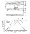
- FIG. 4is a graph showing the change of transmittance according to retardation in a conventional FFS-LCD, a FFS-LCD employing a liquid crystal layer of positive dielectric anisotropy, and a TN-LCD.
- FIGS. 2 and 3are cross-sectional views of FFS-LCD according to the present invention and FIG. 4 is a graph showing the change of transmittance according to retardation in a conventional FFS-LCD, a FFS-LCD employing a liquid crystal layer of positive dielectric anisotropy according to the present invention and a TN-LCD.
- a FFS-LCD of the present inventioncomprises a lower substrate 20 and an upper substrate 40 opposed to each other with a predetermined distance (d: hereinafter referred to as cell gap).
- a cell gap dis 2 to 6 ⁇ m.
- a liquid crystal layer 30is interposed between the lower and upper substrates 20 and 40 , comprising a plurality of liquid crystal molecules 30 a .
- the liquid crystal molecules 30 ahave a positive dielectric anisotropy of 4 to 15.
- a gate bus line and a data bus lineare crossed on the lower substrate 20 to define a unit pixel.
- a thin film transistor(not shown) is disposed at the intersection of the lines.
- a counter electrode 22is formed in a slant or plate shape, comprising a transparent conductive ITO layer. In the preferred embodiment, it is formed in a plate shape.
- a gate insulating layer 24is formed on the lower substrate 20 which has formed the counter electrode 22 thereon.
- a pixel electrode 26is formed on the gate insulating layer 24 in a slant shape to overlap with the counter electrode 22 .
- a distance 1 between the counter electrode 22 and the pixel electrode 26is narrower than a cell gap d, thereby forming a fringe field between the electrodes 22 and 26 .
- a first horizontal alignment layer 28is formed on the surface of the resulting lower substrate 20 to control initial arrangement of liquid crystal molecules.
- the first horizontal alignment layer 28has a rubbing axis forming an angle of 45 to 90°, preferably, 60 to 85° with a substrate projected line of fringe field to be formed between the counter electrode 22 and the pixel electrode 26 .
- a color filter 42is formed on the opposite surface of upper substrate 40 corresponding to the lower substrate 20 .
- a second horizontal alignment layer 44having a rubbing axis forming a predetermined angle with that of the first horizontal alignment layer 28 , for example, 180°.
- a polarizer 45 ais attached on the outer surface of lower substrate 20 for linear polarization of light coming from a backlight (not shown) and a decomposer 45 b is attached on the outer surface of upper substrate 40 for selective absorption and transmission of light passing through a liquid crystal layer 30 .
- the polarizer 45 ahas a polarization axis (not shown) parallel with a rubbing axis of the first horizontal alignment layer 28 and the decomposer 45 b has an absorption axis (not shown) perpendicular to the polarization axis.
- a fringe field switching mode LCDoperates as follows.
- liquid crystal molecules 30 a of positive dielectric anisotropyare arranged, the major axes thereof being parallel with rubbing axes of the first and the second horizontal alignment layers 28 and 44 .
- liquid crystal molecules 30 a of positive dielectric anisotropyare arranged, the major axis thereof being parallel with the fringe field F. Therefore, light has suffered a change of polarizing state in passing through the liquid crystal layer 30 . Accordingly, light is not absorbed by the decomposer 45 b and consequently, the screen becomes white.
- liquid crystal molecules on the surface of alignment layerare arranged depending on the alignment layer due to anchoring force thereof, even if a electric field is formed.
- a distance between the counter electrode 22 and the pixel electrode 26is very narrow, thereby generating an intense electric field between the electrodes, particularly, on the surface of the first horizontal alignment layer 28 .
- liquid crystal molecules of positive dielectric anisotropyare driven more actively since the major axis thereof is twisted in parallel with the electric field.
- FIG. 4shows a change of transmittance according to retardation.
- Ais a graph of transmittance according to retardation in a conventional FFS-LCD
- Bis in a TN-LCD
- Cis in a FFS-LCD employing liquid crystal layer of positive dielectric anisotropy.
- a conventional FFS-LCDhas a maximum transmittance at a retardation of 0.2 to 0.3 ⁇ m
- TN-LCDhas a maximum transmittance at a retardation of 0.4 to 0.5 ⁇ m.
- a maximum transmittanceis obtained at a retardation of 0.3 to 0.45 ⁇ m, which is shifted to a TN-LCD graph B. This is because when a FFS-LCD employs liquid crystal layer of positive dielectric anisotropy, liquid crystal molecules on the surface of the first alignment layer 28 are driven.
- a maximum transmittanceis obtained at a retardation of 0.3 to 0.45 ⁇ m.
Landscapes
- Physics & Mathematics (AREA)
- Nonlinear Science (AREA)
- Mathematical Physics (AREA)
- Chemical & Material Sciences (AREA)
- Crystallography & Structural Chemistry (AREA)
- General Physics & Mathematics (AREA)
- Optics & Photonics (AREA)
- Liquid Crystal (AREA)
- Geometry (AREA)
Abstract
Description
Claims (7)
Applications Claiming Priority (2)
| Application Number | Priority Date | Filing Date | Title |
|---|---|---|---|
| KR2000-36598 | 2000-06-29 | ||
| KR1020000036598AKR20020002134A (en) | 2000-06-29 | 2000-06-29 | Fringe field switching mode lcd |
Publications (2)
| Publication Number | Publication Date |
|---|---|
| US20020008828A1 US20020008828A1 (en) | 2002-01-24 |
| US6678027B2true US6678027B2 (en) | 2004-01-13 |
Family
ID=19674922
Family Applications (1)
| Application Number | Title | Priority Date | Filing Date |
|---|---|---|---|
| US09/894,937Expired - LifetimeUS6678027B2 (en) | 2000-06-29 | 2001-06-28 | Fringe field switching mode LCD |
Country Status (3)
| Country | Link |
|---|---|
| US (1) | US6678027B2 (en) |
| JP (1) | JP2002082357A (en) |
| KR (1) | KR20020002134A (en) |
Cited By (22)
| Publication number | Priority date | Publication date | Assignee | Title |
|---|---|---|---|---|
| US20030025677A1 (en)* | 2001-07-24 | 2003-02-06 | Naohisa Iwamoto | Electromagnetic digitizer and distortion-free LCD |
| US20050062927A1 (en)* | 2003-09-24 | 2005-03-24 | Sharp Kabushiki Kaisha | Liquid crystal display device |
| US20060139504A1 (en)* | 2004-12-24 | 2006-06-29 | Ahn Byung C | Liquid crystal display device and fabricating method thereof |
| US20060146213A1 (en)* | 2004-12-31 | 2006-07-06 | Ahn Byung C | Liquid crystal display device and fabricating method thereof |
| US20060146245A1 (en)* | 2004-12-31 | 2006-07-06 | Ahn Byung C | Liquid crystal display device and fabricating method thereof |
| US20060197893A1 (en)* | 2004-12-10 | 2006-09-07 | Ga-Lane Chen | Transflective display device |
| US20060244873A1 (en)* | 2003-09-24 | 2006-11-02 | Sharp Kabushiki Kaisha | Liquid crystal display device |
| US20060256264A1 (en)* | 2004-05-14 | 2006-11-16 | Innolux Display Corp. | Multi-domain transflective type fringe field switching liquid crystal display |
| US20070020128A1 (en)* | 2005-06-30 | 2007-01-25 | Delta Electronics, Inc. | Dual fan and dual motor structure thereof |
| US20070139572A1 (en)* | 2005-12-16 | 2007-06-21 | Young-Wook Lee | Thin film transistor array panel for liquid crystal display and manufacturing method thereof |
| US20070146295A1 (en)* | 2005-12-22 | 2007-06-28 | Au Optronics Corporation | Circuit and method for improving image quality of a liquid crystal display |
| US20070182901A1 (en)* | 2006-02-09 | 2007-08-09 | Wintek Corporation | Multi-domain liquid crystal display |
| US20070291208A1 (en)* | 2006-06-16 | 2007-12-20 | Wintek Corporation | Multi-domain liquid crystal display |
| US20080204612A1 (en)* | 2007-02-27 | 2008-08-28 | Lachezar Komitov | Liquid crystal device |
| US20090073368A1 (en)* | 2007-09-19 | 2009-03-19 | Wen-Chun Wang | Multi-domain liquid crystal display |
| US20090091669A1 (en)* | 2007-10-04 | 2009-04-09 | Wen-Chun Wang | Multi-domain liquid crystal display and array substrate thereof |
| US20090135342A1 (en)* | 2007-11-26 | 2009-05-28 | Au Optronics Corporation | Wide viewing angle liquid crystal display |
| US7663708B2 (en) | 2006-03-31 | 2010-02-16 | Wintek Corporation | Multi-domain liquid crystal display |
| US8461048B2 (en) | 2010-12-02 | 2013-06-11 | Chunghwa Picture Tubes, Ltd. | Fabrication method of minute pattern |
| US8947608B2 (en) | 2012-04-13 | 2015-02-03 | Samsung Display Co., Ltd. | Display apparatus including electrostatic preventing pattern |
| US9223180B2 (en) | 2012-09-24 | 2015-12-29 | Au Optronics Corporation | Fringe field switching mode liquid crystal display panel |
| US9581850B2 (en) | 2013-10-23 | 2017-02-28 | Au Optronics Corp. | Display panel |
Families Citing this family (16)
| Publication number | Priority date | Publication date | Assignee | Title |
|---|---|---|---|---|
| JP2006337888A (en)* | 2005-06-06 | 2006-12-14 | Sanyo Epson Imaging Devices Corp | Liquid crystal device and electronic apparatus |
| WO2007088644A1 (en) | 2006-01-31 | 2007-08-09 | Casio Computer Co., Ltd. | Liquid crystal display apparatus using an electric field substantially parallel to the substrate surfaces |
| JP4622917B2 (en)* | 2006-03-30 | 2011-02-02 | エプソンイメージングデバイス株式会社 | Array substrate for liquid crystal panel and liquid crystal panel |
| JP2010519587A (en)* | 2007-02-26 | 2010-06-03 | ラヒェザー コミトブ | LCD device |
| JP2009198703A (en)* | 2008-02-20 | 2009-09-03 | Sony Corp | Liquid crystal display device and method of manufacturing the same |
| JP4613973B2 (en) | 2008-03-26 | 2011-01-19 | カシオ計算機株式会社 | Liquid crystal display element |
| JP5075718B2 (en)* | 2008-04-08 | 2012-11-21 | 株式会社ジャパンディスプレイイースト | Liquid crystal display |
| JP5516863B2 (en) | 2009-03-18 | 2014-06-11 | Jsr株式会社 | Liquid crystal aligning agent and liquid crystal display element |
| JP5315136B2 (en)* | 2009-06-05 | 2013-10-16 | 株式会社ジャパンディスプレイ | Liquid crystal display |
| JP5404281B2 (en)* | 2009-09-28 | 2014-01-29 | 株式会社ジャパンディスプレイ | LCD panel |
| TWM433573U (en)* | 2011-01-31 | 2012-07-11 | Hannstar Display Corp | Active matrix liquid crystal display |
| KR101959389B1 (en)* | 2012-04-25 | 2019-03-20 | 삼성디스플레이 주식회사 | Liquid crystal display device |
| JP6315182B2 (en) | 2014-03-18 | 2018-04-25 | Jsr株式会社 | Liquid crystal aligning agent and liquid crystal display element |
| JP6451941B2 (en) | 2014-04-23 | 2019-01-16 | Jsr株式会社 | Liquid crystal aligning agent and liquid crystal display element |
| KR20160025126A (en) | 2014-08-26 | 2016-03-08 | 삼성디스플레이 주식회사 | Liquid crystal display device |
| KR102285754B1 (en) | 2015-01-08 | 2021-08-04 | 삼성디스플레이 주식회사 | Thin film transistor array substrate and method of manufacturing the same |
Citations (5)
| Publication number | Priority date | Publication date | Assignee | Title |
|---|---|---|---|---|
| GB2325751A (en)* | 1997-05-30 | 1998-12-02 | Hyundai Electronics Ind | In-plane switched liquid crystal device |
| KR19990086580A (en)* | 1998-05-29 | 1999-12-15 | 김영환 | LCD Display of IPS Mode |
| KR20000014693A (en)* | 1998-08-24 | 2000-03-15 | 김영환 | Reflective liquid crystal display having high opening rate and high transmittance and fabricating method thereof |
| US6233034B1 (en)* | 1997-12-29 | 2001-05-15 | Hyundai Electronics Industries Co., Ltd. | Liquid crystal display and fabrication method |
| US6466290B2 (en)* | 1999-12-22 | 2002-10-15 | Hyundai Display Technology Inc. | Fringe field switching mode LCD |
Family Cites Families (4)
| Publication number | Priority date | Publication date | Assignee | Title |
|---|---|---|---|---|
| JPH103076A (en)* | 1996-06-17 | 1998-01-06 | Furontetsuku:Kk | Liquid crystal display element |
| KR100286762B1 (en)* | 1997-06-27 | 2001-04-16 | 박종섭 | Liquid crystal display element |
| KR100341123B1 (en)* | 1997-12-29 | 2002-12-18 | 주식회사 현대 디스플레이 테크놀로지 | LCD having high transmittance and high aperture ratio and method for manufacturing the same |
| KR100325065B1 (en)* | 1998-06-30 | 2002-08-24 | 주식회사 현대 디스플레이 테크놀로지 | Reflective liquid crystal display with high brightness and wide viewing angle |
- 2000
- 2000-06-29KRKR1020000036598Apatent/KR20020002134A/ennot_activeCeased
- 2001
- 2001-06-28USUS09/894,937patent/US6678027B2/ennot_activeExpired - Lifetime
- 2001-06-29JPJP2001199854Apatent/JP2002082357A/enactivePending
Patent Citations (10)
| Publication number | Priority date | Publication date | Assignee | Title |
|---|---|---|---|---|
| GB2325751A (en)* | 1997-05-30 | 1998-12-02 | Hyundai Electronics Ind | In-plane switched liquid crystal device |
| US6233034B1 (en)* | 1997-12-29 | 2001-05-15 | Hyundai Electronics Industries Co., Ltd. | Liquid crystal display and fabrication method |
| US6522380B2 (en)* | 1997-12-29 | 2003-02-18 | Hyundai Display Technology Inc. | Liquid crystal display having high transmittance and high aperture ratio |
| KR19990086580A (en)* | 1998-05-29 | 1999-12-15 | 김영환 | LCD Display of IPS Mode |
| US6256081B1 (en)* | 1998-05-29 | 2001-07-03 | Hyundai Electronics Industries Co., Ltd. | LCD of high aperture ratio and high transmittance preventing color shift having transparent pixel and counter electrodes producing oblique electric fields |
| KR20000014693A (en)* | 1998-08-24 | 2000-03-15 | 김영환 | Reflective liquid crystal display having high opening rate and high transmittance and fabricating method thereof |
| US6351300B1 (en)* | 1998-08-24 | 2002-02-26 | Hyundai Display Technology Inc. | Reflective LCD having high transmittance and method for manufacturing the same |
| US20020044248A1 (en)* | 1998-08-24 | 2002-04-18 | In Cheol Park | Reflective LCD having high transmittance and method for manufacturing the same |
| US6452658B1 (en)* | 1998-08-24 | 2002-09-17 | Hyundai Display Technology Inc. | Reflective LCD having high transmittance and method for manufacturing the same |
| US6466290B2 (en)* | 1999-12-22 | 2002-10-15 | Hyundai Display Technology Inc. | Fringe field switching mode LCD |
Cited By (41)
| Publication number | Priority date | Publication date | Assignee | Title |
|---|---|---|---|---|
| US6906694B2 (en)* | 2001-07-24 | 2005-06-14 | Wacom Co., Ltd. | Electromagnetic digitizer and distortion-free LCD |
| US20030025677A1 (en)* | 2001-07-24 | 2003-02-06 | Naohisa Iwamoto | Electromagnetic digitizer and distortion-free LCD |
| US20050062927A1 (en)* | 2003-09-24 | 2005-03-24 | Sharp Kabushiki Kaisha | Liquid crystal display device |
| US7463328B2 (en)* | 2003-09-24 | 2008-12-09 | Sharp Kabushiki Kaisha | Liquid crystal display device with fine particles in liquid crystal layer |
| US7719656B2 (en)* | 2003-09-24 | 2010-05-18 | Sharp Kabushiki Kaisha | Liquid crystal display device |
| US20060244873A1 (en)* | 2003-09-24 | 2006-11-02 | Sharp Kabushiki Kaisha | Liquid crystal display device |
| US20060256264A1 (en)* | 2004-05-14 | 2006-11-16 | Innolux Display Corp. | Multi-domain transflective type fringe field switching liquid crystal display |
| US7495726B2 (en) | 2004-12-10 | 2009-02-24 | Hon Hai Precision Industry Co., Ltd. | Transflective display device |
| US20060197893A1 (en)* | 2004-12-10 | 2006-09-07 | Ga-Lane Chen | Transflective display device |
| US20060139504A1 (en)* | 2004-12-24 | 2006-06-29 | Ahn Byung C | Liquid crystal display device and fabricating method thereof |
| US20100231820A1 (en)* | 2004-12-24 | 2010-09-16 | Byung Chul Ahn | Liquid crystal display device and fabricating method thereof |
| US7751011B2 (en) | 2004-12-24 | 2010-07-06 | Lg Display Co., Ltd. | Method of fabricating a liquid crystal display device, comprising forming a protective film so that one end of the protective film is contacted with one end of the transparent conductive pattern. |
| US8013969B2 (en) | 2004-12-24 | 2011-09-06 | Lg Display Co., Ltd. | Liquid crystal display device comprising a protective film so that the protective film borders with one end of a transparent conductive pattern |
| US20060146245A1 (en)* | 2004-12-31 | 2006-07-06 | Ahn Byung C | Liquid crystal display device and fabricating method thereof |
| US20100237349A1 (en)* | 2004-12-31 | 2010-09-23 | Byung Chul Ahn | Liquid crystal display device and fabricating method thereof |
| US8189162B2 (en) | 2004-12-31 | 2012-05-29 | Lg Display Co., Ltd. | Liquid crystal display device and fabricating method thereof |
| US7760276B2 (en) | 2004-12-31 | 2010-07-20 | Lg Display Co., Ltd. | Liquid crystal display device and fabricating method thereof |
| US20060146213A1 (en)* | 2004-12-31 | 2006-07-06 | Ahn Byung C | Liquid crystal display device and fabricating method thereof |
| US7679699B2 (en) | 2004-12-31 | 2010-03-16 | Lg Display Co., Ltd. | Liquid crystal display device and fabricating method thereof |
| US20070020128A1 (en)* | 2005-06-30 | 2007-01-25 | Delta Electronics, Inc. | Dual fan and dual motor structure thereof |
| US20070139572A1 (en)* | 2005-12-16 | 2007-06-21 | Young-Wook Lee | Thin film transistor array panel for liquid crystal display and manufacturing method thereof |
| US20070146295A1 (en)* | 2005-12-22 | 2007-06-28 | Au Optronics Corporation | Circuit and method for improving image quality of a liquid crystal display |
| US7746330B2 (en) | 2005-12-22 | 2010-06-29 | Au Optronics Corporation | Circuit and method for improving image quality of a liquid crystal display |
| US7619707B2 (en) | 2006-02-09 | 2009-11-17 | Wintek Corporation | Multi-domain liquid crystal display |
| US20070182901A1 (en)* | 2006-02-09 | 2007-08-09 | Wintek Corporation | Multi-domain liquid crystal display |
| US7663708B2 (en) | 2006-03-31 | 2010-02-16 | Wintek Corporation | Multi-domain liquid crystal display |
| US20070291208A1 (en)* | 2006-06-16 | 2007-12-20 | Wintek Corporation | Multi-domain liquid crystal display |
| US7973897B2 (en) | 2006-06-16 | 2011-07-05 | Wintek Corporation | Multi-domain liquid crystal display |
| US20080204612A1 (en)* | 2007-02-27 | 2008-08-28 | Lachezar Komitov | Liquid crystal device |
| US7876385B2 (en)* | 2007-02-27 | 2011-01-25 | Lachezar Komitov | Liquid crystal device |
| US20090073368A1 (en)* | 2007-09-19 | 2009-03-19 | Wen-Chun Wang | Multi-domain liquid crystal display |
| US8330923B2 (en) | 2007-09-19 | 2012-12-11 | Wintek Corporation | Multi-domain liquid crystal display |
| US20090091669A1 (en)* | 2007-10-04 | 2009-04-09 | Wen-Chun Wang | Multi-domain liquid crystal display and array substrate thereof |
| US7924385B2 (en) | 2007-11-26 | 2011-04-12 | Au Optronics Corporation | Wide viewing angle liquid crystal display comprising at least one floating electrode in locations directly facing a corresponding one or more pixel electrodes thereby inducing an electric field in the liquid crystal layer |
| US20090135342A1 (en)* | 2007-11-26 | 2009-05-28 | Au Optronics Corporation | Wide viewing angle liquid crystal display |
| USRE44167E1 (en) | 2007-11-26 | 2013-04-23 | Au Optronics Corporation | Wide viewing angle liquid crystal display comprising at least one floating electrode in locations facing corresponding one or more pixel electrodes with liquid crystal layer therebetween |
| US8461048B2 (en) | 2010-12-02 | 2013-06-11 | Chunghwa Picture Tubes, Ltd. | Fabrication method of minute pattern |
| US8947608B2 (en) | 2012-04-13 | 2015-02-03 | Samsung Display Co., Ltd. | Display apparatus including electrostatic preventing pattern |
| US9223180B2 (en) | 2012-09-24 | 2015-12-29 | Au Optronics Corporation | Fringe field switching mode liquid crystal display panel |
| US9535298B2 (en) | 2012-09-24 | 2017-01-03 | Au Optronics Corporation | Fringe-field switching mode liquid crystal display panel |
| US9581850B2 (en) | 2013-10-23 | 2017-02-28 | Au Optronics Corp. | Display panel |
Also Published As
| Publication number | Publication date |
|---|---|
| KR20020002134A (en) | 2002-01-09 |
| JP2002082357A (en) | 2002-03-22 |
| US20020008828A1 (en) | 2002-01-24 |
Similar Documents
| Publication | Publication Date | Title |
|---|---|---|
| US6678027B2 (en) | Fringe field switching mode LCD | |
| US6266118B1 (en) | Liquid crystal display of high aperture ratio and high transmittance having multi-domain having transparent conductive pixel and counter electrodes on the same substrate | |
| KR100293811B1 (en) | LCD display device of IP PS mode | |
| US6466290B2 (en) | Fringe field switching mode LCD | |
| KR101147127B1 (en) | Liquid Crystal Display Device And Dribing Method Thereof | |
| JP2002031812A (en) | Fringe field switching mode liquid crystal display device | |
| JPH1124068A (en) | Method for forming dual domain inside liquid crystal layer, manufacture of liquid crystal display device using the method and liquid crystal display device | |
| JPH11242233A (en) | Horizontal electric field type liquid crystal display device | |
| JP3549177B2 (en) | Liquid crystal display | |
| US6392731B1 (en) | Liquid crystal display device | |
| US6876425B2 (en) | LCD device implementing FLCP orientation film | |
| WO2012090838A1 (en) | Liquid-crystal panel and liquid-crystal display | |
| KR20030061584A (en) | 2-domain ffs-va mode liquid crystal display device | |
| JPH103076A (en) | Liquid crystal display element | |
| US6320637B1 (en) | Liquid crystal display with wide viewing angle | |
| KR100306806B1 (en) | Liquid crystal display | |
| KR100599952B1 (en) | High aperture and high transmittance liquid crystal display with improved response speed | |
| KR101774280B1 (en) | In-Plane Switching Mode Liquid Crystal Display Device And Method Of Driving The Same | |
| KR100305638B1 (en) | Twist Nema Kick LCD Display | |
| KR100957567B1 (en) | Liquid crystal display panel and liquid crystal display device having same | |
| JP3099817B2 (en) | Liquid crystal display | |
| KR100674231B1 (en) | Fringe Field Drive Mode Liquid Crystal Display | |
| JP3922014B2 (en) | Liquid crystal display | |
| KR101812542B1 (en) | In-Plane Switching Mode Liquid Crystal Display Device And Method Of Driving The Same | |
| KR100658059B1 (en) | Twisted nematic liquid crystal display with improved viewing angle |
Legal Events
| Date | Code | Title | Description |
|---|---|---|---|
| AS | Assignment | Owner name:HYNIX SEMICONDUCTOR INC., KOREA, REPUBLIC OF Free format text:ASSIGNMENT OF ASSIGNORS INTEREST;ASSIGNORS:PARK, CHI HYUCK;KIM, JIN MAHN;LEE, SEUNG HEE;AND OTHERS;REEL/FRAME:011956/0426 Effective date:20010620 | |
| AS | Assignment | Owner name:HYUNDAI DISPLAY TECHNOLOGY INC., KOREA, REPUBLIC O Free format text:ASSIGNMENT OF ASSIGNORS INTEREST;ASSIGNOR:HYNIX SEMICONDUCTOR INC.;REEL/FRAME:012287/0925 Effective date:20011023 | |
| AS | Assignment | Owner name:BOE-HYDIS TECHNOLOGY CO., LTD., KOREA, REPUBLIC OF Free format text:ASSIGNMENT OF ASSIGNORS INTEREST;ASSIGNOR:HYUNDAI DISPLAY TECHNOLOGY, INC.;REEL/FRAME:013879/0345 Effective date:20030303 | |
| FEPP | Fee payment procedure | Free format text:PAYOR NUMBER ASSIGNED (ORIGINAL EVENT CODE: ASPN); ENTITY STATUS OF PATENT OWNER: LARGE ENTITY | |
| STCF | Information on status: patent grant | Free format text:PATENTED CASE | |
| FPAY | Fee payment | Year of fee payment:4 | |
| FEPP | Fee payment procedure | Free format text:PAYER NUMBER DE-ASSIGNED (ORIGINAL EVENT CODE: RMPN); ENTITY STATUS OF PATENT OWNER: LARGE ENTITY | |
| FPAY | Fee payment | Year of fee payment:8 | |
| FPAY | Fee payment | Year of fee payment:12 |