US6677645B2 - Body contact MOSFET - Google Patents
Body contact MOSFETDownload PDFInfo
- Publication number
- US6677645B2 US6677645B2US10/061,263US6126302AUS6677645B2US 6677645 B2US6677645 B2US 6677645B2US 6126302 AUS6126302 AUS 6126302AUS 6677645 B2US6677645 B2US 6677645B2
- Authority
- US
- United States
- Prior art keywords
- gate
- body contact
- insulator
- layer
- transistor
- Prior art date
- Legal status (The legal status is an assumption and is not a legal conclusion. Google has not performed a legal analysis and makes no representation as to the accuracy of the status listed.)
- Expired - Lifetime
Links
Images


Classifications
- H—ELECTRICITY
- H10—SEMICONDUCTOR DEVICES; ELECTRIC SOLID-STATE DEVICES NOT OTHERWISE PROVIDED FOR
- H10D—INORGANIC ELECTRIC SEMICONDUCTOR DEVICES
- H10D30/00—Field-effect transistors [FET]
- H10D30/01—Manufacture or treatment
- H10D30/021—Manufacture or treatment of FETs having insulated gates [IGFET]
- H10D30/031—Manufacture or treatment of FETs having insulated gates [IGFET] of thin-film transistors [TFT]
- H10D30/0321—Manufacture or treatment of FETs having insulated gates [IGFET] of thin-film transistors [TFT] comprising silicon, e.g. amorphous silicon or polysilicon
- H10D30/0323—Manufacture or treatment of FETs having insulated gates [IGFET] of thin-film transistors [TFT] comprising silicon, e.g. amorphous silicon or polysilicon comprising monocrystalline silicon
- H—ELECTRICITY
- H10—SEMICONDUCTOR DEVICES; ELECTRIC SOLID-STATE DEVICES NOT OTHERWISE PROVIDED FOR
- H10D—INORGANIC ELECTRIC SEMICONDUCTOR DEVICES
- H10D30/00—Field-effect transistors [FET]
- H10D30/60—Insulated-gate field-effect transistors [IGFET]
- H10D30/67—Thin-film transistors [TFT]
- H10D30/6704—Thin-film transistors [TFT] having supplementary regions or layers in the thin films or in the insulated bulk substrates for controlling properties of the device
- H10D30/6708—Thin-film transistors [TFT] having supplementary regions or layers in the thin films or in the insulated bulk substrates for controlling properties of the device for preventing the kink effect or the snapback effect, e.g. discharging the minority carriers of the channel region for preventing bipolar effect
- H10D30/6711—Thin-film transistors [TFT] having supplementary regions or layers in the thin films or in the insulated bulk substrates for controlling properties of the device for preventing the kink effect or the snapback effect, e.g. discharging the minority carriers of the channel region for preventing bipolar effect by using electrodes contacting the supplementary regions or layers
Definitions
- This inventiongenerally relates to field effect transistors, and more specifically relates to body contact field effect transistors formed in silicon-on-insulator technology.
- a conventional transistorhas a source region and a drain region spaced apart by an intervening body region. All of these regions are planar, and are controlled by a gate.
- the body regionis the area from which electron hole pair generation takes place that allows current to be carried between the source and drain regions underneath the gate. By contacting the body region, a charge may be applied that changes the voltage at which the transistor turns on. This is often referred to as a Vt adjustment because the threshold voltage of the device is being adjusted with this technique.
- Silicon-on-insulator (SOI) technologyemploys a layer of semiconductor material overlying an insulation layer on a supporting bulk wafer.
- the structurecomprises a film of crystalline silicon on a buried layer of silicon oxide on a crystalline silicon substrate.
- SOI technologymakes possible certain performance advantages, such as a reduction in parasitic capacitance, useful in the semiconductor industry.
- the bodyIn a non-SOI transistor the body is automatically contacted simply because it forms part of the same silicon substrate on which all devices sit, and is either grounded via contact to the backside of the chip so the bodies of all the devices are grounded, or tied to the power supply via the N-well.
- the body of the transistorOn a SOI wafer, however, the body of the transistor is separated from whatever devices may be separately connected to the wafer by the buried oxide layer. SOI technology where the body is not connected to anything-called a floating body device-may suffer from the problem of hysteresis: the body retains charge and some of the electrical properties from the last time the transistor was used, interfering with subsequent use of the device.
- body contactsallow the threshold voltage to be changed so that standby power can be reduced for low-power applications.
- Body contacts in SOIhave conventionally been made by creating a T-shaped structure on the diffusion, thereby creating three distinct regions: a source, a drain, and a body contact region. This approach leads to decreased performance in that it yields a greatly increased gate capacitance over a conventional device, often leading to very poor performance. Therefore, there exists a need for a body contact in SOI processes that allows precise control of the body potential but that does not lead to the poor performance that comes from high gate capacitance.
- the present inventionprovides a body contact structure that overcomes the disadvantages of the prior art by utilizing an insulating structure between the body contact portion of the active area and the transistor portion of the active area.
- the present inventionprovides an insulative structure formed across the active area that isolates the portion of the area where transistors are formed from the portions of the active area where the body contact is formed. The body contact produced by these methods adds no significant gate capacitance to the device.
- the present inventioncan be implemented using a variety of fabrication methods. Each fabrication method forms the insulative structure between the transistor portion of the active area and the body contact portion of the active area, but does so in a variety of different ways.
- One methodsubstitutes an insulator for at least a portion of the gate layer in the regions between the transistor and the body contact.
- Another methodremoves a portion of the gate layer and replaces it with an insulative layer in regions between the transistor and the body contact.
- Still anotherforms the insulative structure by forming multiple layers, or thicker layers, of gate dielectric between the gate and the body in regions between the transistor and the body contact.
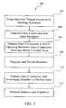
- FIG. 1is a flow diagram illustrating a first fabrication method according to a first embodiment of the present invention
- FIGS. 2-8are top and cross-sectional side views of an exemplary body contact transistor during fabrication
- FIG. 9is a flow diagram illustrating a second fabrication method according to the embodiment of the preceding figures.
- FIGS. 10-14are top and cross-sectional side views of a second exemplary body contact transistor during fabrication
- FIG. 15is a flow diagram illustrating a third fabrication method according to the embodiment of the preceding figures.
- FIGS. 16-21are top and cross-sectional side views of a third exemplary body contact transistor during fabrication
- FIG. 22is a flow diagram illustrating a fabrication method according to a second embodiment of the present invention.
- FIGS. 23-27are top views of a fourth exemplary body contact transistor during fabrication
- FIG. 28is a cross-sectional side view of an existing thin oxide T-body contact
- FIG. 29is a cross-sectional side view of fifth exemplary body contact
- FIG. 30is a flow diagram illustrating a fabrication method according another embodiment of the present invention.
- FIG. 31is a top view of a sixth exemplary body contact.
- FIG. 32is a top view of another embodiment of the body contact of FIG. 31 .
- the present inventionprovides a body contact structure that overcomes the disadvantages of the prior art.
- the present inventionutilizes an insulator structure between the body contact portion of the active area and the transistor portion.
- the present inventionprovides a raised insulative structure, comprising an element distinct from the gate, formed across the active area that isolates the portion of the area where transistors are formed from the portions of the active area where the body contact is formed.
- the body contactthus produced adds no significant gate capacitance to the gate.
- the transistor and body contact portionsare formed in a substantially coplanar semiconducting substrate.
- the present inventioncan be implemented using a variety of fabrication methods. These methods form the insulative structure between the transistor portion of the active area and the body contact portion of the active area in a variety of different ways. One such method substitutes an insulator for at least a portion of the gate layer in the regions between the transistor and the body contact. Another method forms the insulative structure by forming a thicker layer of gate dielectric between the gate and the body in regions between the transistor and the body contact. Still another removes a portion of the gate layer and replaces it with an insulative layer in regions between the transistor and the body contact.
- the non-performing portion of a conventional T-gateis provided for the insulation it offers between the active FET portions of the active area and the body contact area, but is not an active part of the transistor. Instead, it represents a significant amount of area that creates non-functional, non-productive capacitance between the body and the gate.
- the present inventionreplaces the non-performming portion of the T-gate body contact with an insulating portion that does not contribute to parasitic capacitance, thus increasing performance.
- the semiconducting substrate where the transistors and the body contact are formedis substantially coplanar. Note that the insulating portion of the body contact does not form a part of the gate, but is a distinct element.
- a SOI device having no body contactis referred to as a floating body MOSFET device.
- a floating body MOSFET deviceIn some applications, however, there exists a need to contact the body under the NFET and PFET devices, so that the body potential may be accurately controlled. These applications include circuits where it is important that the body voltage be an exact value, and those where matching to other devices is crucial. Specific examples include analog mode sense amplifier circuits and phase locked loops. Additionally, body contacted devices can be useful for low power applications, since the Vt is adjustable.
- the present inventionmakes use of the OP (silicide block) level and the fact that the source/drain implants may be separately defined. Additionally, an embodiment of the invention makes use of the fact that multiple gate oxides may be made available on the same wafer by using the thicker oxide design (DG) level over the body contact region while still using the thinner oxide over the FET channel region for improved performance.
- the present inventionprovides a gate, one portion of which is an insulator, and places that insulator such that the source and drain regions are isolated from the body contact region of the device. The body contact thus produced adds no significant gate capacitance to the device.
- Method 100forms the insulative structure by substituting an insulator for at least a portion of the gate layer in the regions between the transistor and the body contact.
- a first step 102 of method 100is to provide a starting substrate and form a shallow trench isolation therein.
- the starting substratecomprises a silicon-on-insulator (SOI) wafer, which in turn comprises a buried oxide (BOX) layer beneath an SOI layer.
- SOIsilicon-on-insulator
- BOXburied oxide
- non-SOI waferscan also be used. When a non-SOI wafer is used, the processing remains identical to that of the SOI wafer case, except as noted.
- the starting substratecomprises an active area 117 that has been provided with a shallow trench isolation layer 118 .
- Isolation layer 118overlies a BOX layer 120 .
- FIG. 2Aillustrates a top view of the active area 117
- FIG. 2Billustrates a cross-sectional side view taken at line 2 B of FIG. 2 A. In each of FIGS.
- FIG. 1represents a top view of the active area and the figure labeled “B” represents a cross sectional view taken along the line shown in the figure labeled “A.”
- a gate dielectric layeris formed in a conventional manner and deposited over active area 117 .
- a second step 104 of method 100is to deposit a gate conductor layer over the substrate.
- the gate conductor layermay comprise polysilicon, or any other suitable conductive layer.
- a polysilicon layer 122has been deposited over shallow trench isolation layer 118 .
- Polysilicon layer 122forms the gate of the transistor in the pictured embodiment, but other materials may also be used as the gate material.
- a third step 106 of method 100is to pattern the gate conductor to form an opening between the gate conductor area and the body contact area. Through this opening, an insulator will be installed, as will be further described below, in order to accomplish the goal of reducing parasitic capacitance.
- One method of forming this openingis to apply a first gate mask over the gate material and etch away the gate material left unprotected by the mask.
- a first gate mask 124is formed over polysilicon layer 122 .
- Mask 124is continuous everywhere except at a gap 126 , the function of which will be explained below.
- Mask 124may be formed from any suitable material, such as silicon nitride or photo resist. Mask 124 would typically be patterned using photoresist and then used to pattern the underlying polysilicon layer 122 . Mask 124 is adapted to protect polysilicon layer 122 from the etching process that removes all polysilicon not so protected.
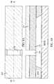
- a fourth step 108 of method 100is to deposit and polish an insulating material in the gap left in the polysilicon by the etching process.
- FIGS. 5A and 5 Bshow an insulator 128 placed in gap 126 of FIGS. 4A and 4B. Insulator 128 , which may be an oxide material, separates the body contact from the source/drain region.
- a fifth step 110 of method 100is shown to be the second patterning of the gate conductor.
- One method of doing thisis to apply a second gate mask over the gate material, and then etch the unprotected material away.
- FIGS. 6A and 6Bshow a second gate mask 130 placed over polysilicon layer 122 .
- mask 130is selective to oxide so that when the gate is patterned, the insulator will remain in place rather than getting etched out.
- FIGS. 7A and 7Bshow the condition of active area 117 after the etching process has been completed. Note that second mask 130 has been removed in FIGS.
- insulator 128a strip 132 of polysilicon layer 122 remains on active area 117 . Also remaining is insulator 128 . Together, insulator 128 and polysilicon strip 132 form a T-shaped body 134 , when seen in the top view of FIG. 7 A.
- a sixth step 112 of method 100is to deposit spacers and implants onto active area 117 . This is depicted in FIGS. 8A and 8B, where sidewall spacers 136 surround insulator 128 and polysilicon strip 132 . Sidewall spacers 136 separate the edge of the conductive gate material from the source/drain implants. Source/drain implants 138 are placed near polysilicon strip 132 , while body contact implants 140 are placed near insulator 128 . Interconnects 142 serve as connections to the body contact area, and may be formed in any conventional manner.
- Method 200offers an alternate way to form the insulative structure by substituting an insulator for at least a portion of the gate layer in the regions between the transistor and the body contact.
- a shallow trench isolationis formed in a starting substrate.
- a second step 204is to deposit a gate conductor, and a third step 206 is to pattern the gate conductor.
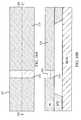
- a fourth step 208is to deposit and polish an insulator and then etch it back a little so it's not as thick as it was in method 100 . This is depicted in FIGS. 10A and 10B, where an insulator 216 has been deposited on an active area 217 over a polysilicon layer 218 . As seen in FIG. 10B, insulator 216 has been etched back such that a slot 220 is created in polysilicon layer 218 .
- a fifth step 210 of method 200is to deposit another layer of gate conductor and polish it flat with the top surface of the gate.
- FIGS. 11A and 11Bshow a second layer of polysilicon 222 overlying substantially all of active area 217 , including insulator 216 .
- Slot 220shown in FIG. 10B, has also been filled with polysilicon 222 .
- the portion of polysilicon layer 222 that fills slot 220will be referred to herein as a plug 226 .
- a sixth step 212 of method 200is to again pattern the gate conductor, which may be accomplished by applying a second gate mask and etching the polysilicon a second time.
- a second gate mask 224which may have a “T” shape as shown, is placed over that portion of the polysilicon which is to remain after the etching process is complete.
- plug 226 of polysiliconhas been placed over insulator 216 , and plug 226 would conventionally be covered by mask 224 or it will be etched away, exposing insulator 216 .
- FIGS. 13A and 13Bshows the appearance of active area 217 after the etching process is complete. Note that a T-shaped gate 228 has been created on the substrate, and that insulator 216 remains covered by polysilicon plug 226 .
- a seventh step 214 of method 200is to deposit spacers and implants on active area 217 .
- Interconnects 242serve as connections to the body contact area, and may be formed in any conventional manner.
- Method 300is yet another way to form the insulative structure by substituting an insulator for at least a portion of the gate layer in the regions between the transistor and the body contact.
- Method 300shares some steps with methods 200 and 100 , but also includes certain steps that are not part of methods 200 and 100 , as will be illustrated below.
- a first step 302 of method 300is to deposit pad nitride over silicon on a wafer.
- a second step 304is to form a shallow trench isolation (STI) in the substrate.
- FIGS. 16A and 16Bdepict an active area 317 on which a pad nitride layer 316 is formed.
- Pad nitride layer 316protects the SOI regions embodied here as a BOX layer 318 .
- a third step 306is to form a mask over the pad nitride layer and strip away all the pad nitride not protected by that mask.
- FIGS. 17A and 17Bshow a pad nitride region 322 left behind after the stripping process.
- a fourth step 308 of method 300is to deposit a gate conductor.
- the gate conductormay also be polished flat with the top surface of the gate, though this step is optional. This step is shown in more detail in FIGS. 18A and 18B, where pad nitride region 322 has been covered by a polysilicon layer 324 .
- a fifth step 310 of method 300is to pattern the gate conductor. As was described in connection with FIGS. 1 and 9, one method of doing this is to apply a gate mask and etch the gate material. Referring to FIGS. 19A and 19B, a gate mask 326 has been applied over gate material 324 . Note that gate mask 326 has the form of a “T,” although, as has been explained, other shapes and forms are also possible. FIGS. 20A and 20B depict active area 317 after the gate material has been etched away. A gate 328 remains on active area 317 , part of which covers pad nitride region 322 .
- a sixth step 312 of method 300is to deposit spacers and implants on active area 317 .
- FIGS. 21A and 21Bshow active area 317 after this has been done. Specifically, sidewall spacers 330 surround gate 328 , and a body contact region 332 and a source/drain region 334 have been added near gate 328 . Interconnects 342 serve as connections to the body contact area, and, as before, may be formed in any conventional manner.
- Method 400removes a portion of the gate layer and replaces it with an insulative layer in regions between the transistor and the body contact.
- a starting substrateis patterned and provided with isolating trenches in a conventional manner.
- FIG. 23shows an exposed active area 417 surrounded by an STI trench 420 .
- One of ordinary skill in the artwill recognize this as part of a conventional transistor fabrication process.
- a second step 404 of method 400is to deposit and pattern a gate conductor. This too forms part of a conventional fabrication process.
- a gate 422includes a horizontal arm 424 and a vertical leg 426 .
- Gate 422may comprise polysilicon, but may also be constructed of any other suitable gate conductor material, such as silicon germanium or a metal.
- gate 422has a T-shaped body, although other bodies, such as H-shaped bodies, may also be used, as has been mentioned.
- a third step 406 of method 400is to install spacers, implants, and silicide. Like steps 402 and 404 , step 406 represents part of a conventional fabrication process.
- FIG. 24indicates that a sidewall spacer 428 surrounds gate 422 . Source/drain implants 430 and a body contact implant 432 rest on active area 417 . An arrow 434 indicates that the underlying substrate is left at the native doping of the well.
- a fourth step 408 of method 400is to apply a gate mask adapted to remove a portion of the gate conductor material
- a fifth step 410is to etch the gate conductor in accordance with the mask applied in step 408 .
- FIG. 25shows that a gate mask 436 has been deposited over gate 422 . Note that gate mask 436 entirely exposes horizontal arm 424 and exposes just a small portion of vertical leg 426 , which allows for normal dimensional on alignment errors.
- FIG. 26depicts active area 417 after the etching step has been completed. An area 438 is the former location of horizontal arm 424 of gate 422 . Arm 424 has been etched away and no longer exists on active area 417 . Vertical leg 426 has been left behind in the etch process, and occupies the position it did before the performance of fifth step 410 . By removing horizontal arm 424 , method 400 eliminates a significant source of parasitic capacitance, leading to a more efficient product.
- a sixth step 412 of method 400involves conventional BEOL processing and contact implantation. Active area 417 after sixth step 412 has been performed is depicted in FIG. 27, where interconnects 442 have been installed. Interconnects 442 serve as connections to the body contact area, and may be formed in any conventional manner.
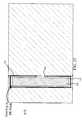
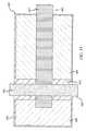
- a cross-sectional side view of a conventional T-body contact 450is shown.
- a buried oxide (BOX) layer 452underlies a STI trench 454 .
- a body contact region 456 and a source/drain region 458rest on BOX layer 452 .
- a native doping region 460is formed in between regions 456 and 458 .
- Conventional T-body contact 450further includes a thin gate-oxide layer 462 , over which is located gate conductor 464 . As has been mentioned in a number of places in the foregoing description, a great deal of parasitic capacitance may build up between the various layers of conventional T-body contact 450 .
- T-body contact 470according to another embodiment of the present invention is illustrated.
- This embodimentmay be referred to a dual gate (DG) embodiment because it comprises dual insulative structures, i.e., dual gate oxide materials, having different thicknesses. In other embodiments, more than two different thicknesses of insulative materials may be used.
- T-body contact 470differs from conventional T-body contact 450 in that a thick gate-oxide layer 476 has replaced a portion of a thin gate-oxide layer 472 between a gate conductor 474 and a body contact region 478 .
- Thick gate-oxide layer 476reduces capacitance between the various layers of T-body contact 470 so that there is less capacitance in the configuration of FIG. 29 than there is in the configuration of FIG. 28 .
- the FIG. 29 configurationmay not reduce capacitance as effectively or to the degree that certain other embodiments of the present invention do.
- Method 500forms a layer of nitride between the body contact region and the source/drain region of the transistor which prevents silicide from forming between the two regions. This leaves a gap that acts as an insulator.
- a first step 502 and a second step 504 of method 500mirror first and second steps 402 and 404 of method 400 , and will thus not be further described here.
- a third step 506 of method 500is to perform spacers and implants, as is conventional in the fabrication process.
- a fourth step 508 of method 500is to deposit a nitride layer and pattern it with an OP mask.
- a fifth step 510is to deposit metal and form silicide, as is conventional during fabrication.
- An optional sixth step 512is to remove the nitride layer, but nitride may also be left in place if desired without affecting the operation of the transistor of this embodiment.
- a seventh step 514is to perform conventional BEOL processing and deposit contacts. Method 500 will be further discussed in connection with FIGS. 31 and 32 below.
- FIG. 31depicts a T-body contact according to an embodiment of the present invention created by method 500 .
- T-body 486comprises a horizontal leg 487 and a vertical leg 488 , as in certain of the other embodiments of the present invention discussed herein.
- only horizontal leg 487comprises a gate conductor;
- vertical leg 488comprises a thin nitride (OP) shape 490 that is deposited after the gate conductor shape is in place.
- OPthin nitride
- OP shape 490temporarily leaves a film of nitride between a body contact region 482 and a source/drain region 484 before the formation of a silicide layer 480 on exposed silicon conductors. This nitride film prevents silicide from forming, thus preventing silicide layer 480 from bridging across regions 482 and 484 .
- OP shape 490may be removed, although in at least one embodiment it may be left in place. Whether or not OP layer 490 is removed, its presence during the fabrication process leaves a gap 492 in silicide layer 480 .
- Gap 492is sufficiently wide that silicide will not wander between regions 482 and 484 , even if OP shape 490 is removed prior to subsequent MOL processing.
- a portion of the gate conductoris once again replaced with an insulative structure, but the replacement occurs after the gate is formed, and the insulative structure need not be left in place.
- FIG. 32an alternate configuration of the OP embodiment is shown.
- OP shape 490has been reduced in length to resemble an L-shape rather than a T-shape, so as to facilitate shorting body 486 to source region 484 .
- Some applicationsrequire this configuration, including input transistors to sense amplifiers and current mirrors.
- This L-shape configurationmay be used with any of the embodiments of the present invention.
- a variety of fabrication methods for a transistor according to the present inventionhave been described. Other methods may also exist.
- the foregoing descriptionhas described selected embodiments of a body contact structure that overcomes the disadvantages of the prior art by utilizing an insulating structure between the body contact portion of the active area and the transistor portion of the active area.
- the description hereinhas discussed a raised insulative structure formed across the active area that isolates the portion of the area where transistors are formed from the portions of the active area where the body contact is formed.
- the body contact produced by these methodsadds no significant gate capacitance to the device.
Landscapes
- Thin Film Transistor (AREA)
- Insulated Gate Type Field-Effect Transistor (AREA)
- Electrodes Of Semiconductors (AREA)
Abstract
Description
Claims (11)
Priority Applications (2)
| Application Number | Priority Date | Filing Date | Title |
|---|---|---|---|
| US10/061,263US6677645B2 (en) | 2002-01-31 | 2002-01-31 | Body contact MOSFET |
| US10/687,333US6940130B2 (en) | 2002-01-31 | 2003-10-16 | Body contact MOSFET |
Applications Claiming Priority (1)
| Application Number | Priority Date | Filing Date | Title |
|---|---|---|---|
| US10/061,263US6677645B2 (en) | 2002-01-31 | 2002-01-31 | Body contact MOSFET |
Related Child Applications (1)
| Application Number | Title | Priority Date | Filing Date |
|---|---|---|---|
| US10/687,333DivisionUS6940130B2 (en) | 2002-01-31 | 2003-10-16 | Body contact MOSFET |
Publications (2)
| Publication Number | Publication Date |
|---|---|
| US20030141543A1 US20030141543A1 (en) | 2003-07-31 |
| US6677645B2true US6677645B2 (en) | 2004-01-13 |
Family
ID=27610142
Family Applications (2)
| Application Number | Title | Priority Date | Filing Date |
|---|---|---|---|
| US10/061,263Expired - LifetimeUS6677645B2 (en) | 2002-01-31 | 2002-01-31 | Body contact MOSFET |
| US10/687,333Expired - Fee RelatedUS6940130B2 (en) | 2002-01-31 | 2003-10-16 | Body contact MOSFET |
Family Applications After (1)
| Application Number | Title | Priority Date | Filing Date |
|---|---|---|---|
| US10/687,333Expired - Fee RelatedUS6940130B2 (en) | 2002-01-31 | 2003-10-16 | Body contact MOSFET |
Country Status (1)
| Country | Link |
|---|---|
| US (2) | US6677645B2 (en) |
Cited By (10)
| Publication number | Priority date | Publication date | Assignee | Title |
|---|---|---|---|---|
| US7011980B1 (en) | 2005-05-09 | 2006-03-14 | International Business Machines Corporation | Method and structures for measuring gate tunneling leakage parameters of field effect transistors |
| US20060175661A1 (en)* | 2005-02-08 | 2006-08-10 | Taiwan Semiconductor Manufacturing Co., Ltd. | SOI MOSFET device with reduced polysilicon loading on active area |
| US20090243029A1 (en)* | 2008-03-26 | 2009-10-01 | Anderson Brent A | Method, structure and design structure for customizing history effects of soi circuits |
| US20090242985A1 (en)* | 2008-03-26 | 2009-10-01 | Anderson Brent A | Method, structure and design structure for customizing history effects of soi circuits |
| US20090243000A1 (en)* | 2008-03-26 | 2009-10-01 | Anderson Brent A | Method, structure and design structure for customizing history effects of soi circuits |
| US20120313174A1 (en)* | 2008-08-11 | 2012-12-13 | International Business Machines Corporation | Method of making a mosfet having self-aligned silicided schottky body tie including intentional pull-down of an sti exposing sidewalls of a diffusion region |
| US20150123206A1 (en)* | 2013-11-04 | 2015-05-07 | Mediatek Inc. | Body-contact metal-oxide-semiconductor field effect transistor device |
| US9177968B1 (en) | 2014-09-19 | 2015-11-03 | Silanna Semiconductor U.S.A., Inc. | Schottky clamped radio frequency switch |
| US11476279B2 (en) | 2020-08-06 | 2022-10-18 | Globalfoundries U.S. Inc. | Devices with staggered body contacts |
| US12199147B2 (en) | 2022-05-02 | 2025-01-14 | GlobalFoundaries U.S. Inc. | Semiconductor device including a body contact region and method of forming the same |
Families Citing this family (43)
| Publication number | Priority date | Publication date | Assignee | Title |
|---|---|---|---|---|
| JP2002261292A (en)* | 2000-12-26 | 2002-09-13 | Toshiba Corp | Semiconductor device and manufacturing method thereof |
| US6804502B2 (en) | 2001-10-10 | 2004-10-12 | Peregrine Semiconductor Corporation | Switch circuit and method of switching radio frequency signals |
| JP2003318405A (en)* | 2002-04-25 | 2003-11-07 | Mitsubishi Electric Corp | Semiconductor device and method of manufacturing the same |
| US7719343B2 (en) | 2003-09-08 | 2010-05-18 | Peregrine Semiconductor Corporation | Low noise charge pump method and apparatus |
| EP3570374B1 (en) | 2004-06-23 | 2022-04-20 | pSemi Corporation | Integrated rf front end |
| US20080076371A1 (en) | 2005-07-11 | 2008-03-27 | Alexander Dribinsky | Circuit and method for controlling charge injection in radio frequency switches |
| USRE48965E1 (en) | 2005-07-11 | 2022-03-08 | Psemi Corporation | Method and apparatus improving gate oxide reliability by controlling accumulated charge |
| US8742502B2 (en) | 2005-07-11 | 2014-06-03 | Peregrine Semiconductor Corporation | Method and apparatus for use in improving linearity of MOSFETs using an accumulated charge sink-harmonic wrinkle reduction |
| US9653601B2 (en) | 2005-07-11 | 2017-05-16 | Peregrine Semiconductor Corporation | Method and apparatus for use in improving linearity of MOSFETs using an accumulated charge sink-harmonic wrinkle reduction |
| US7910993B2 (en) | 2005-07-11 | 2011-03-22 | Peregrine Semiconductor Corporation | Method and apparatus for use in improving linearity of MOSFET's using an accumulated charge sink |
| US7890891B2 (en) | 2005-07-11 | 2011-02-15 | Peregrine Semiconductor Corporation | Method and apparatus improving gate oxide reliability by controlling accumulated charge |
| US20070045698A1 (en)* | 2005-08-31 | 2007-03-01 | International Business Machines Corporation | Semiconductor structures with body contacts and fabrication methods thereof |
| US8587062B2 (en)* | 2007-03-26 | 2013-11-19 | International Business Machines Corporation | Silicon on insulator (SOI) field effect transistors (FETs) with adjacent body contacts |
| US7960772B2 (en) | 2007-04-26 | 2011-06-14 | Peregrine Semiconductor Corporation | Tuning capacitance to enhance FET stack voltage withstand |
| US20090057742A1 (en)* | 2007-08-30 | 2009-03-05 | Sungjae Lee | Cmos varactor |
| US9024700B2 (en) | 2008-02-28 | 2015-05-05 | Peregrine Semiconductor Corporation | Method and apparatus for use in digitally tuning a capacitor in an integrated circuit device |
| EP2421132A2 (en) | 2008-07-18 | 2012-02-22 | Peregrine Semiconductor Corporation | Charge pump with a plurality of transfer control switches |
| US9030248B2 (en)* | 2008-07-18 | 2015-05-12 | Peregrine Semiconductor Corporation | Level shifter with output spike reduction |
| US9660590B2 (en) | 2008-07-18 | 2017-05-23 | Peregrine Semiconductor Corporation | Low-noise high efficiency bias generation circuits and method |
| JP2010040896A (en)* | 2008-08-07 | 2010-02-18 | Nec Electronics Corp | Semiconductor device |
| US8680617B2 (en)* | 2009-10-06 | 2014-03-25 | International Business Machines Corporation | Split level shallow trench isolation for area efficient body contacts in SOI MOSFETS |
| US8441071B2 (en) | 2010-01-05 | 2013-05-14 | International Business Machines Corporation | Body contacted transistor with reduced parasitic capacitance |
| CN102148158B (en)* | 2010-02-09 | 2013-03-27 | 中国科学院微电子研究所 | Body contact device structure and manufacturing method thereof |
| US20120105095A1 (en)* | 2010-11-03 | 2012-05-03 | International Business Machines Corporation | Silicon-on-insulator (soi) body-contact pass gate structure |
| US9264053B2 (en) | 2011-01-18 | 2016-02-16 | Peregrine Semiconductor Corporation | Variable frequency charge pump |
| US9590674B2 (en) | 2012-12-14 | 2017-03-07 | Peregrine Semiconductor Corporation | Semiconductor devices with switchable ground-body connection |
| US20150236748A1 (en) | 2013-03-14 | 2015-08-20 | Peregrine Semiconductor Corporation | Devices and Methods for Duplexer Loss Reduction |
| US9406695B2 (en) | 2013-11-20 | 2016-08-02 | Peregrine Semiconductor Corporation | Circuit and method for improving ESD tolerance and switching speed |
| US9196544B2 (en)* | 2014-03-14 | 2015-11-24 | Globalfoundries Singapore Pte. Ltd. | Integrated circuits with stressed semiconductor-on-insulator (SOI) body contacts and methods for fabricating the same |
| US9831857B2 (en) | 2015-03-11 | 2017-11-28 | Peregrine Semiconductor Corporation | Power splitter with programmable output phase shift |
| US10944008B2 (en)* | 2015-12-08 | 2021-03-09 | Skyworks Solutions, Inc. | Low noise amplifier transistors with decreased noise figure and leakage in silicon-on-insulator technology |
| US9948281B2 (en) | 2016-09-02 | 2018-04-17 | Peregrine Semiconductor Corporation | Positive logic digitally tunable capacitor |
| US9997360B2 (en)* | 2016-09-21 | 2018-06-12 | Qualcomm Incorporated | Method for mitigating layout effect in FINFET |
| US10672885B2 (en)* | 2017-10-19 | 2020-06-02 | Newport Fab, Llc | Silicide block isolation for reducing off-capacitance of a radio frequency (RF) switch |
| US10586870B2 (en) | 2018-02-20 | 2020-03-10 | Newport Fab, Llc | Wide contact structure for small footprint radio frequency (RF) switch |
| US10325833B1 (en) | 2018-02-20 | 2019-06-18 | Newport Fab, Llc | Bent polysilicon gate structure for small footprint radio frequency (RF) switch |
| US10236872B1 (en) | 2018-03-28 | 2019-03-19 | Psemi Corporation | AC coupling modules for bias ladders |
| US10886911B2 (en) | 2018-03-28 | 2021-01-05 | Psemi Corporation | Stacked FET switch bias ladders |
| US10505530B2 (en) | 2018-03-28 | 2019-12-10 | Psemi Corporation | Positive logic switch with selectable DC blocking circuit |
| US11476849B2 (en) | 2020-01-06 | 2022-10-18 | Psemi Corporation | High power positive logic switch |
| CN112349783B (en)* | 2020-11-05 | 2022-04-05 | 武汉新芯集成电路制造有限公司 | Semiconductor device and method for manufacturing the same |
| CN118398668B (en)* | 2024-06-27 | 2024-11-12 | 武汉新芯集成电路股份有限公司 | Semiconductor device and method for manufacturing the same |
| CN118431299A (en)* | 2024-07-05 | 2024-08-02 | 武汉新芯集成电路股份有限公司 | Semiconductor device and method for manufacturing the same |
Citations (27)
| Publication number | Priority date | Publication date | Assignee | Title |
|---|---|---|---|---|
| US4577390A (en)* | 1983-02-23 | 1986-03-25 | Texas Instruments Incorporated | Fabrication of polysilicon to polysilicon capacitors with a composite dielectric layer |
| JPS6430851A (en) | 1987-07-28 | 1989-02-01 | Kito Kk | Truck crane |
| US4965213A (en) | 1988-02-01 | 1990-10-23 | Texas Instruments Incorporated | Silicon-on-insulator transistor with body node to source node connection |
| US5079605A (en) | 1988-07-29 | 1992-01-07 | Texas Instruments Incorporated | Silicon-on-insulator transistor with selectable body node to source node connection |
| US5089870A (en)* | 1989-06-19 | 1992-02-18 | L'etat Francais Represente Par Le Ministre Des Postes, Des Telecommunications Et De L'espace (Centre National D'etudes Des Telecommunications) | Soi mos transistor with a substrate-source connection |
| US5126817A (en)* | 1989-10-13 | 1992-06-30 | Kabushiki Kaisha Toshiba | Dielectrically isolated structure for use in soi-type semiconductor device |
| US5145802A (en) | 1991-11-12 | 1992-09-08 | United Technologies Corporation | Method of making SOI circuit with buried connectors |
| US5160989A (en) | 1989-06-13 | 1992-11-03 | Texas Instruments Incorporated | Extended body contact for semiconductor over insulator transistor |
| US5185280A (en) | 1991-01-29 | 1993-02-09 | Texas Instruments Incorporated | Method of fabricating a soi transistor with pocket implant and body-to-source (bts) contact |
| US5298773A (en) | 1992-08-17 | 1994-03-29 | United Technologies Corporation | Silicon-on-insulator H-transistor layout for gate arrays |
| US5317181A (en) | 1992-09-10 | 1994-05-31 | United Technologies Corporation | Alternative body contact for fully-depleted silicon-on-insulator transistors |
| US5324683A (en)* | 1993-06-02 | 1994-06-28 | Motorola, Inc. | Method of forming a semiconductor structure having an air region |
| US5424225A (en) | 1988-11-25 | 1995-06-13 | Mitsubishi Denki Kabushiki Kaisha | Method of manufacturing a thin film SOI MOSFET |
| US5489792A (en)* | 1994-04-07 | 1996-02-06 | Regents Of The University Of California | Silicon-on-insulator transistors having improved current characteristics and reduced electrostatic discharge susceptibility |
| US5559368A (en) | 1994-08-30 | 1996-09-24 | The Regents Of The University Of California | Dynamic threshold voltage mosfet having gate to body connection for ultra-low voltage operation |
| US5811855A (en) | 1997-12-29 | 1998-09-22 | United Technologies Corporation | SOI combination body tie |
| US5818085A (en) | 1995-11-09 | 1998-10-06 | Taiwan Semiconductor Manufacturing Company, Ltd. | Body contact for a MOSFET device fabricated in an SOI layer |
| US5821575A (en) | 1996-05-20 | 1998-10-13 | Digital Equipment Corporation | Compact self-aligned body contact silicon-on-insulator transistor |
| US5831320A (en) | 1995-12-02 | 1998-11-03 | Lg Semicon Co., Ltd. | High voltage metal oxide silicon field effect transistor |
| US5872383A (en)* | 1996-06-24 | 1999-02-16 | Kabushiki Kaisha Toshiba | Semiconductor device and method of manufacturing the same |
| US5929490A (en) | 1997-04-17 | 1999-07-27 | Nec Corporation | Semiconductor device with an improved body contact hole structure |
| US5962895A (en) | 1994-06-29 | 1999-10-05 | International Business Machines Corporation | SOI transistor having a self-aligned body contact |
| US5973364A (en) | 1997-09-19 | 1999-10-26 | Kabushiki Kaisha Toshiba | MIS semiconductor device having body-contact region |
| US6084255A (en) | 1998-01-29 | 2000-07-04 | Mitsubishi Denki Kabushiki Kaisha | Gate array semiconductor device |
| US6261921B1 (en)* | 1999-07-31 | 2001-07-17 | Taiwan Semiconductor Manufacturing Co., Ltd. | Method of forming shallow trench isolation structure |
| US6281593B1 (en)* | 1999-12-06 | 2001-08-28 | International Business Machines Corporation | SOI MOSFET body contact and method of fabrication |
| US6344671B1 (en)* | 1999-12-14 | 2002-02-05 | International Business Machines Corporation | Pair of FETs including a shared SOI body contact and the method of forming the FETs |
Family Cites Families (1)
| Publication number | Priority date | Publication date | Assignee | Title |
|---|---|---|---|---|
| US6620656B2 (en)* | 2001-12-19 | 2003-09-16 | Motorola, Inc. | Method of forming body-tied silicon on insulator semiconductor device |
- 2002
- 2002-01-31USUS10/061,263patent/US6677645B2/ennot_activeExpired - Lifetime
- 2003
- 2003-10-16USUS10/687,333patent/US6940130B2/ennot_activeExpired - Fee Related
Patent Citations (29)
| Publication number | Priority date | Publication date | Assignee | Title |
|---|---|---|---|---|
| US4577390A (en)* | 1983-02-23 | 1986-03-25 | Texas Instruments Incorporated | Fabrication of polysilicon to polysilicon capacitors with a composite dielectric layer |
| JPS6430851A (en) | 1987-07-28 | 1989-02-01 | Kito Kk | Truck crane |
| US4965213A (en) | 1988-02-01 | 1990-10-23 | Texas Instruments Incorporated | Silicon-on-insulator transistor with body node to source node connection |
| US5079605A (en) | 1988-07-29 | 1992-01-07 | Texas Instruments Incorporated | Silicon-on-insulator transistor with selectable body node to source node connection |
| US5424225A (en) | 1988-11-25 | 1995-06-13 | Mitsubishi Denki Kabushiki Kaisha | Method of manufacturing a thin film SOI MOSFET |
| US5160989A (en) | 1989-06-13 | 1992-11-03 | Texas Instruments Incorporated | Extended body contact for semiconductor over insulator transistor |
| US5089870A (en)* | 1989-06-19 | 1992-02-18 | L'etat Francais Represente Par Le Ministre Des Postes, Des Telecommunications Et De L'espace (Centre National D'etudes Des Telecommunications) | Soi mos transistor with a substrate-source connection |
| US5126817A (en)* | 1989-10-13 | 1992-06-30 | Kabushiki Kaisha Toshiba | Dielectrically isolated structure for use in soi-type semiconductor device |
| US5185280A (en) | 1991-01-29 | 1993-02-09 | Texas Instruments Incorporated | Method of fabricating a soi transistor with pocket implant and body-to-source (bts) contact |
| US5145802A (en) | 1991-11-12 | 1992-09-08 | United Technologies Corporation | Method of making SOI circuit with buried connectors |
| US5298773A (en) | 1992-08-17 | 1994-03-29 | United Technologies Corporation | Silicon-on-insulator H-transistor layout for gate arrays |
| US5317181A (en) | 1992-09-10 | 1994-05-31 | United Technologies Corporation | Alternative body contact for fully-depleted silicon-on-insulator transistors |
| US5324683A (en)* | 1993-06-02 | 1994-06-28 | Motorola, Inc. | Method of forming a semiconductor structure having an air region |
| US5489792A (en)* | 1994-04-07 | 1996-02-06 | Regents Of The University Of California | Silicon-on-insulator transistors having improved current characteristics and reduced electrostatic discharge susceptibility |
| US5982003A (en) | 1994-04-07 | 1999-11-09 | The Regents Of The University Of California | Silicon-on-insulator transistors having improved current characteristics and reduced electrostatic discharge susceptibility |
| US5962895A (en) | 1994-06-29 | 1999-10-05 | International Business Machines Corporation | SOI transistor having a self-aligned body contact |
| US5559368A (en) | 1994-08-30 | 1996-09-24 | The Regents Of The University Of California | Dynamic threshold voltage mosfet having gate to body connection for ultra-low voltage operation |
| US5818085A (en) | 1995-11-09 | 1998-10-06 | Taiwan Semiconductor Manufacturing Company, Ltd. | Body contact for a MOSFET device fabricated in an SOI layer |
| US5831320A (en) | 1995-12-02 | 1998-11-03 | Lg Semicon Co., Ltd. | High voltage metal oxide silicon field effect transistor |
| US5821575A (en) | 1996-05-20 | 1998-10-13 | Digital Equipment Corporation | Compact self-aligned body contact silicon-on-insulator transistor |
| US5930605A (en) | 1996-05-20 | 1999-07-27 | Digital Equipment Corporation | Compact self-aligned body contact silicon-on-insulator transistors |
| US5872383A (en)* | 1996-06-24 | 1999-02-16 | Kabushiki Kaisha Toshiba | Semiconductor device and method of manufacturing the same |
| US5929490A (en) | 1997-04-17 | 1999-07-27 | Nec Corporation | Semiconductor device with an improved body contact hole structure |
| US5973364A (en) | 1997-09-19 | 1999-10-26 | Kabushiki Kaisha Toshiba | MIS semiconductor device having body-contact region |
| US5811855A (en) | 1997-12-29 | 1998-09-22 | United Technologies Corporation | SOI combination body tie |
| US6084255A (en) | 1998-01-29 | 2000-07-04 | Mitsubishi Denki Kabushiki Kaisha | Gate array semiconductor device |
| US6261921B1 (en)* | 1999-07-31 | 2001-07-17 | Taiwan Semiconductor Manufacturing Co., Ltd. | Method of forming shallow trench isolation structure |
| US6281593B1 (en)* | 1999-12-06 | 2001-08-28 | International Business Machines Corporation | SOI MOSFET body contact and method of fabrication |
| US6344671B1 (en)* | 1999-12-14 | 2002-02-05 | International Business Machines Corporation | Pair of FETs including a shared SOI body contact and the method of forming the FETs |
Cited By (22)
| Publication number | Priority date | Publication date | Assignee | Title |
|---|---|---|---|---|
| US7723787B2 (en) | 2005-02-08 | 2010-05-25 | Taiwan Semiconductor Manufacturing Co., Ltd. | SOI MOSFET device with reduced polysilicon loading on active area |
| US20060175661A1 (en)* | 2005-02-08 | 2006-08-10 | Taiwan Semiconductor Manufacturing Co., Ltd. | SOI MOSFET device with reduced polysilicon loading on active area |
| US7453122B2 (en)* | 2005-02-08 | 2008-11-18 | Taiwan Semiconductor Manufacturing Co., Ltd. | SOI MOSFET device with reduced polysilicon loading on active area |
| US20090039429A1 (en)* | 2005-02-08 | 2009-02-12 | Taiwan Semiconductor Manufacturing Co., Ltd. | Soi mosfet device with reduced polysilicon loading on active area |
| US7011980B1 (en) | 2005-05-09 | 2006-03-14 | International Business Machines Corporation | Method and structures for measuring gate tunneling leakage parameters of field effect transistors |
| US8410554B2 (en) | 2008-03-26 | 2013-04-02 | International Business Machines Corporation | Method, structure and design structure for customizing history effects of SOI circuits |
| US9286425B2 (en) | 2008-03-26 | 2016-03-15 | Globalfoundries Inc. | Method, structure and design structure for customizing history effects of SOI circuits |
| US20090242985A1 (en)* | 2008-03-26 | 2009-10-01 | Anderson Brent A | Method, structure and design structure for customizing history effects of soi circuits |
| US7964467B2 (en) | 2008-03-26 | 2011-06-21 | International Business Machines Corporation | Method, structure and design structure for customizing history effects of soi circuits |
| US20090243029A1 (en)* | 2008-03-26 | 2009-10-01 | Anderson Brent A | Method, structure and design structure for customizing history effects of soi circuits |
| US8420460B2 (en) | 2008-03-26 | 2013-04-16 | International Business Machines Corporation | Method, structure and design structure for customizing history effects of SOI circuits |
| US8963211B2 (en) | 2008-03-26 | 2015-02-24 | International Business Machines Corporation | Method, structure and design structure for customizing history effects of SOI circuits |
| US20090243000A1 (en)* | 2008-03-26 | 2009-10-01 | Anderson Brent A | Method, structure and design structure for customizing history effects of soi circuits |
| US9349852B2 (en) | 2008-03-26 | 2016-05-24 | Globalfoundries Inc. | Method, structure and design structure for customizing history effects of SOI circuits |
| US20120313174A1 (en)* | 2008-08-11 | 2012-12-13 | International Business Machines Corporation | Method of making a mosfet having self-aligned silicided schottky body tie including intentional pull-down of an sti exposing sidewalls of a diffusion region |
| US9620640B2 (en)* | 2013-11-04 | 2017-04-11 | Mediatek Inc. | Body-contact metal-oxide-semiconductor field effect transistor device |
| US20150123206A1 (en)* | 2013-11-04 | 2015-05-07 | Mediatek Inc. | Body-contact metal-oxide-semiconductor field effect transistor device |
| US9177968B1 (en) | 2014-09-19 | 2015-11-03 | Silanna Semiconductor U.S.A., Inc. | Schottky clamped radio frequency switch |
| US9502433B2 (en) | 2014-09-19 | 2016-11-22 | Qualcomm Incorporated | Schottky clamped radio frequency switch |
| US11476279B2 (en) | 2020-08-06 | 2022-10-18 | Globalfoundries U.S. Inc. | Devices with staggered body contacts |
| US11804491B2 (en) | 2020-08-06 | 2023-10-31 | Globalfoundries U.S. Inc. | Devices with staggered body contacts |
| US12199147B2 (en) | 2022-05-02 | 2025-01-14 | GlobalFoundaries U.S. Inc. | Semiconductor device including a body contact region and method of forming the same |
Also Published As
| Publication number | Publication date |
|---|---|
| US6940130B2 (en) | 2005-09-06 |
| US20040079995A1 (en) | 2004-04-29 |
| US20030141543A1 (en) | 2003-07-31 |
Similar Documents
| Publication | Publication Date | Title |
|---|---|---|
| US6677645B2 (en) | Body contact MOSFET | |
| KR100189966B1 (en) | Soy-structured MOS transistor and manufacturing method thereof | |
| US6200866B1 (en) | Use of silicon germanium and other alloys as the replacement gate for the fabrication of MOSFET | |
| US6403405B1 (en) | Method of manufacturing SOI element having body contact | |
| US6437405B2 (en) | Silicon-on-insulator (SOI) substrate, method for fabricating SOI substrate and SOI MOSFET using the SOI substrate | |
| JP3965064B2 (en) | Method for forming an integrated circuit having a body contact | |
| US8455938B2 (en) | Device comprising a field-effect transistor in a silicon-on-insulator | |
| US20060038216A1 (en) | Formation of capacitor having a Fin structure | |
| KR20040065297A (en) | Body-tied silicon on insulator semiconductor device and method therefor | |
| US6664150B2 (en) | Active well schemes for SOI technology | |
| JP5527922B2 (en) | Differentiated SOI structure without oxide buried under DC node diffusion region and having oxide hole | |
| US7135742B1 (en) | Insulated gate type semiconductor device and method for fabricating same | |
| US20050023608A1 (en) | Method of forming a partially depleted silicon on insulator (PDSOI) transistor with a pad lock body extension | |
| US6555915B1 (en) | Integrated circuit having interconnect to a substrate and method therefor | |
| US20010002058A1 (en) | Semiconductor apparatus and method of manufacture | |
| KR101326393B1 (en) | Semiconductor device | |
| US6077747A (en) | Method of manufacturing semiconductor device | |
| JP3529220B2 (en) | Semiconductor device and manufacturing method thereof | |
| KR100318458B1 (en) | Method of isolation in SOI device | |
| US20080012075A1 (en) | Silicon-on-insulator semiconductor device | |
| JPH1012885A (en) | Semiconductor device and manufacturing method thereof | |
| JP2000332250A (en) | Semiconductor device and manufacturing method thereof | |
| US20050158923A1 (en) | Ultra-thin body transistor with recessed silicide contacts | |
| KR0155840B1 (en) | MOS transistor and manufacturing method thereof | |
| US20040061175A1 (en) | Full depletion SOI-MOS transistor |
Legal Events
| Date | Code | Title | Description |
|---|---|---|---|
| AS | Assignment | Owner name:INTERNATIONAL BUSINESS MACHINES CORPORATION, NEW Y Free format text:ASSIGNMENT OF ASSIGNORS INTEREST;ASSIGNORS:BRYANT, ANDRES;COTTRELL, PETER E.;ELLIS-MONAGHAN, JOHN J.;AND OTHERS;REEL/FRAME:012568/0076;SIGNING DATES FROM 20020103 TO 20020126 | |
| FEPP | Fee payment procedure | Free format text:PAYOR NUMBER ASSIGNED (ORIGINAL EVENT CODE: ASPN); ENTITY STATUS OF PATENT OWNER: LARGE ENTITY | |
| STCF | Information on status: patent grant | Free format text:PATENTED CASE | |
| FPAY | Fee payment | Year of fee payment:4 | |
| FPAY | Fee payment | Year of fee payment:8 | |
| FPAY | Fee payment | Year of fee payment:12 | |
| AS | Assignment | Owner name:GLOBALFOUNDRIES U.S. 2 LLC, NEW YORK Free format text:ASSIGNMENT OF ASSIGNORS INTEREST;ASSIGNOR:INTERNATIONAL BUSINESS MACHINES CORPORATION;REEL/FRAME:036550/0001 Effective date:20150629 | |
| AS | Assignment | Owner name:GLOBALFOUNDRIES INC., CAYMAN ISLANDS Free format text:ASSIGNMENT OF ASSIGNORS INTEREST;ASSIGNORS:GLOBALFOUNDRIES U.S. 2 LLC;GLOBALFOUNDRIES U.S. INC.;REEL/FRAME:036779/0001 Effective date:20150910 | |
| AS | Assignment | Owner name:WILMINGTON TRUST, NATIONAL ASSOCIATION, DELAWARE Free format text:SECURITY AGREEMENT;ASSIGNOR:GLOBALFOUNDRIES INC.;REEL/FRAME:049490/0001 Effective date:20181127 | |
| AS | Assignment | Owner name:GLOBALFOUNDRIES U.S. INC., CALIFORNIA Free format text:ASSIGNMENT OF ASSIGNORS INTEREST;ASSIGNOR:GLOBALFOUNDRIES INC.;REEL/FRAME:054633/0001 Effective date:20201022 | |
| AS | Assignment | Owner name:GLOBALFOUNDRIES INC., CAYMAN ISLANDS Free format text:RELEASE BY SECURED PARTY;ASSIGNOR:WILMINGTON TRUST, NATIONAL ASSOCIATION;REEL/FRAME:054636/0001 Effective date:20201117 | |
| AS | Assignment | Owner name:GLOBALFOUNDRIES U.S. INC., NEW YORK Free format text:RELEASE BY SECURED PARTY;ASSIGNOR:WILMINGTON TRUST, NATIONAL ASSOCIATION;REEL/FRAME:056987/0001 Effective date:20201117 |