US6677204B2 - Multigate semiconductor device with vertical channel current and method of fabrication - Google Patents
Multigate semiconductor device with vertical channel current and method of fabricationDownload PDFInfo
- Publication number
- US6677204B2 US6677204B2US10/254,878US25487802AUS6677204B2US 6677204 B2US6677204 B2US 6677204B2US 25487802 AUS25487802 AUS 25487802AUS 6677204 B2US6677204 B2US 6677204B2
- Authority
- US
- United States
- Prior art keywords
- parallel lines
- charge storage
- forming
- lines
- region
- Prior art date
- Legal status (The legal status is an assumption and is not a legal conclusion. Google has not performed a legal analysis and makes no representation as to the accuracy of the status listed.)
- Expired - Fee Related, expires
Links
Images


Classifications
- H—ELECTRICITY
- H10—SEMICONDUCTOR DEVICES; ELECTRIC SOLID-STATE DEVICES NOT OTHERWISE PROVIDED FOR
- H10B—ELECTRONIC MEMORY DEVICES
- H10B41/00—Electrically erasable-and-programmable ROM [EEPROM] devices comprising floating gates
- H10B41/20—Electrically erasable-and-programmable ROM [EEPROM] devices comprising floating gates characterised by three-dimensional arrangements, e.g. with cells on different height levels
- H10B41/23—Electrically erasable-and-programmable ROM [EEPROM] devices comprising floating gates characterised by three-dimensional arrangements, e.g. with cells on different height levels with source and drain on different levels, e.g. with sloping channels
- H10B41/27—Electrically erasable-and-programmable ROM [EEPROM] devices comprising floating gates characterised by three-dimensional arrangements, e.g. with cells on different height levels with source and drain on different levels, e.g. with sloping channels the channels comprising vertical portions, e.g. U-shaped channels
- H—ELECTRICITY
- H10—SEMICONDUCTOR DEVICES; ELECTRIC SOLID-STATE DEVICES NOT OTHERWISE PROVIDED FOR
- H10B—ELECTRONIC MEMORY DEVICES
- H10B43/00—EEPROM devices comprising charge-trapping gate insulators
- H10B43/30—EEPROM devices comprising charge-trapping gate insulators characterised by the memory core region
- H—ELECTRICITY
- H10—SEMICONDUCTOR DEVICES; ELECTRIC SOLID-STATE DEVICES NOT OTHERWISE PROVIDED FOR
- H10B—ELECTRONIC MEMORY DEVICES
- H10B69/00—Erasable-and-programmable ROM [EPROM] devices not provided for in groups H10B41/00 - H10B63/00, e.g. ultraviolet erasable-and-programmable ROM [UVEPROM] devices
- H—ELECTRICITY
- H10—SEMICONDUCTOR DEVICES; ELECTRIC SOLID-STATE DEVICES NOT OTHERWISE PROVIDED FOR
- H10D—INORGANIC ELECTRIC SEMICONDUCTOR DEVICES
- H10D30/00—Field-effect transistors [FET]
- H10D30/01—Manufacture or treatment
- H10D30/021—Manufacture or treatment of FETs having insulated gates [IGFET]
- H10D30/0411—Manufacture or treatment of FETs having insulated gates [IGFET] of FETs having floating gates
- H—ELECTRICITY
- H10—SEMICONDUCTOR DEVICES; ELECTRIC SOLID-STATE DEVICES NOT OTHERWISE PROVIDED FOR
- H10D—INORGANIC ELECTRIC SEMICONDUCTOR DEVICES
- H10D30/00—Field-effect transistors [FET]
- H10D30/01—Manufacture or treatment
- H10D30/021—Manufacture or treatment of FETs having insulated gates [IGFET]
- H10D30/0413—Manufacture or treatment of FETs having insulated gates [IGFET] of FETs having charge-trapping gate insulators, e.g. MNOS transistors
- H—ELECTRICITY
- H10—SEMICONDUCTOR DEVICES; ELECTRIC SOLID-STATE DEVICES NOT OTHERWISE PROVIDED FOR
- H10D—INORGANIC ELECTRIC SEMICONDUCTOR DEVICES
- H10D30/00—Field-effect transistors [FET]
- H10D30/60—Insulated-gate field-effect transistors [IGFET]
- H10D30/68—Floating-gate IGFETs
- H10D30/681—Floating-gate IGFETs having only two programming levels
- H—ELECTRICITY
- H10—SEMICONDUCTOR DEVICES; ELECTRIC SOLID-STATE DEVICES NOT OTHERWISE PROVIDED FOR
- H10D—INORGANIC ELECTRIC SEMICONDUCTOR DEVICES
- H10D64/00—Electrodes of devices having potential barriers
- H10D64/01—Manufacture or treatment
- H10D64/031—Manufacture or treatment of data-storage electrodes
- H10D64/035—Manufacture or treatment of data-storage electrodes comprising conductor-insulator-conductor-insulator-semiconductor structures
- H—ELECTRICITY
- H10—SEMICONDUCTOR DEVICES; ELECTRIC SOLID-STATE DEVICES NOT OTHERWISE PROVIDED FOR
- H10D—INORGANIC ELECTRIC SEMICONDUCTOR DEVICES
- H10D64/00—Electrodes of devices having potential barriers
- H10D64/01—Manufacture or treatment
- H10D64/031—Manufacture or treatment of data-storage electrodes
- H10D64/037—Manufacture or treatment of data-storage electrodes comprising charge-trapping insulators
- G—PHYSICS
- G11—INFORMATION STORAGE
- G11C—STATIC STORES
- G11C11/00—Digital stores characterised by the use of particular electric or magnetic storage elements; Storage elements therefor
- G11C11/56—Digital stores characterised by the use of particular electric or magnetic storage elements; Storage elements therefor using storage elements with more than two stable states represented by steps, e.g. of voltage, current, phase, frequency
- G11C11/5621—Digital stores characterised by the use of particular electric or magnetic storage elements; Storage elements therefor using storage elements with more than two stable states represented by steps, e.g. of voltage, current, phase, frequency using charge storage in a floating gate
- G—PHYSICS
- G11—INFORMATION STORAGE
- G11C—STATIC STORES
- G11C11/00—Digital stores characterised by the use of particular electric or magnetic storage elements; Storage elements therefor
- G11C11/56—Digital stores characterised by the use of particular electric or magnetic storage elements; Storage elements therefor using storage elements with more than two stable states represented by steps, e.g. of voltage, current, phase, frequency
- G11C11/5671—Digital stores characterised by the use of particular electric or magnetic storage elements; Storage elements therefor using storage elements with more than two stable states represented by steps, e.g. of voltage, current, phase, frequency using charge trapping in an insulator
- G—PHYSICS
- G11—INFORMATION STORAGE
- G11C—STATIC STORES
- G11C16/00—Erasable programmable read-only memories
- G11C16/02—Erasable programmable read-only memories electrically programmable
- G11C16/04—Erasable programmable read-only memories electrically programmable using variable threshold transistors, e.g. FAMOS
- G11C16/0408—Erasable programmable read-only memories electrically programmable using variable threshold transistors, e.g. FAMOS comprising cells containing floating gate transistors
- G11C16/0441—Erasable programmable read-only memories electrically programmable using variable threshold transistors, e.g. FAMOS comprising cells containing floating gate transistors comprising cells containing multiple floating gate devices, e.g. separate read-and-write FAMOS transistors with connected floating gates
- G11C16/0458—Erasable programmable read-only memories electrically programmable using variable threshold transistors, e.g. FAMOS comprising cells containing floating gate transistors comprising cells containing multiple floating gate devices, e.g. separate read-and-write FAMOS transistors with connected floating gates comprising two or more independent floating gates which store independent data
- G—PHYSICS
- G11—INFORMATION STORAGE
- G11C—STATIC STORES
- G11C16/00—Erasable programmable read-only memories
- G11C16/02—Erasable programmable read-only memories electrically programmable
- G11C16/04—Erasable programmable read-only memories electrically programmable using variable threshold transistors, e.g. FAMOS
- G11C16/0466—Erasable programmable read-only memories electrically programmable using variable threshold transistors, e.g. FAMOS comprising cells with charge storage in an insulating layer, e.g. metal-nitride-oxide-silicon [MNOS], silicon-oxide-nitride-oxide-silicon [SONOS]
- G11C16/0475—Erasable programmable read-only memories electrically programmable using variable threshold transistors, e.g. FAMOS comprising cells with charge storage in an insulating layer, e.g. metal-nitride-oxide-silicon [MNOS], silicon-oxide-nitride-oxide-silicon [SONOS] comprising two or more independent storage sites which store independent data
- G—PHYSICS
- G11—INFORMATION STORAGE
- G11C—STATIC STORES
- G11C2211/00—Indexing scheme relating to digital stores characterized by the use of particular electric or magnetic storage elements; Storage elements therefor
- G11C2211/56—Indexing scheme relating to G11C11/56 and sub-groups for features not covered by these groups
- G11C2211/561—Multilevel memory cell aspects
- G11C2211/5611—Multilevel memory cell with more than one control gate
- G—PHYSICS
- G11—INFORMATION STORAGE
- G11C—STATIC STORES
- G11C2211/00—Indexing scheme relating to digital stores characterized by the use of particular electric or magnetic storage elements; Storage elements therefor
- G11C2211/56—Indexing scheme relating to G11C11/56 and sub-groups for features not covered by these groups
- G11C2211/561—Multilevel memory cell aspects
- G11C2211/5612—Multilevel memory cell with more than one floating gate
Definitions
- the present inventionrelates to the field of nonvolatile memories and more specifically to a multibit nonvolatile memory and its method of fabrication.
- nonvolatile memory devicewhich can be easily fabricated in a dense array, so that large amounts of data can be stored in a nonvolatile manner.
- a silicon channel body having a first and second channel surfaceis formed.
- a charge storage mediumis formed adjacent to the first channel surface and a second charge storage medium is formed adjacent to the second channel surface.
- a first control gateis formed adjacent to the first charge storage medium adjacent to the first channel surface and a second control gate is formed adjacent to the second charge storage medium adjacent to the second surface.
- a transistoris provided that has a source, a channel, a drain, and a plurality of gates where the channel current flows vertically between the source and drain.
- a memory elementis formed using a transistor that has a read current that flows in a direction perpendicular to a substrate in or over which the transistor is formed.
- the transistorhas a charge storage medium for storing its state. Multiple control gates address the transistor.
- FIGS. 1 a and 1 bare illustrations of isometric views of a pillar memory or transistor having multiple gates in accordance with the present invention.
- FIG. 1 cis an illustration of an overhead view of the pillar memory or transistor shown in FIGS. 1 a and 1 b.
- FIG. 1 dis a graph which illustrates the ability to simultaneously store and read multiple bits of information from a single pillar memory in accordance with the present invention.
- FIGS. 2 a - 2 rillustrates a method of fabricating a multigate transistor or, memory having a vertical read current in accordance with the present invention.
- the present inventionis a novel multigate semiconductor device having vertical channel current and its method of fabrication.
- numerous specific detailsare set forth in order to provide a thorough understanding of the present invention.
- One of ordinary skill in the artwill appreciate that these specific details are not necessary to practice the present invention.
- well-known semiconductor memory layout and processing techniqueshave not been described in specific detail in order to not unnecessarily obscure the present invention.
- the present inventionis a novel multigate semiconductor device and its method of fabrication.
- the multigate semiconductor devicecan be used as a multibit nonvolatile memory or as a multiple gate transistor.
- the present inventionwill be described with respect to a multibit nonvolatile memory.
- a multibit nonvolatile memory 100 in accordance with the present inventionis illustrated in FIGS. 1 a - 1 c.
- Nonvolatile memory device 100includes a pillar 102 .
- Pillar 102comprises a stack of film providing a first source/drain region 104 , a channel or body region 106 , and a second source/drain region 108 formed on the channel region.
- the pillarincludes a first source/drain region 104 formed from a heavily doped N+ single crystal silicon film having a doping density in the range between 1 ⁇ 10 19 to 1 ⁇ 10 20 atoms/cm 3 , a body 106 formed from a P type single crystal silicon film having a doping density between 1 ⁇ 10 16 to 1 ⁇ 10 18 atoms/cm 3 and a second source/drain region 108 formed from a heavily doped N+ single crystal silicon film having a doping density between 1 ⁇ 10 19 to 1 ⁇ 10 20 atoms/cm 3 .
- the N+ source/drain regions 104 and 108can have thickness between 500-1000 ⁇ .
- the thickness of the P type silicon bodydefines the channel length of the device (i.e., the distance between the source and drain region).
- the thickness of the P type body 106can be between 1000-7000 ⁇ and is dependent upon the programming voltages desired for the device. For low programming voltages (e.g., 4-5 volts) the P type silicon film 106 can have a thickness between 1000-2500 ⁇ while for higher programming voltages (e.g., 6-10 volts) a P type silicon film having a thickness between 6000-7000 ⁇ can be used.
- the pillar 102is formed so the first source/drain region 104 , the body 106 , and the second source/drain region 108 are each vertically aligned over one another as shown in FIG. 1 a.
- the pillar 102is formed in a rectangular or square pattern so that the pillar has four separate faces or sides 110 , 111 , 112 , and 113 as shown in FIG. 1 c. Pillar 102 has two faces 110 and 112 which are along laterally opposite sides and two other faces 111 and 113 which are formed along laterally opposite sides.
- charge storage medium 114 , 115 , 116 , and 117are formed from a deposited oxide having H+ ions contained therein.
- a H+ containing oxideacts as a charge trapping dielectric enabling it to store charge therein.
- the charge storage mediums 114 - 117are a silicon oxide-silicon nitride-silicon oxide (i.e., ONO) dielectric stack.
- the charge storage mediums 114 - 117can be nanocrystals isolated by a tunnel dielectric from pillar 102 and isolated from a control gate by a control gate dielectric.
- the charge storage mediumis a continuous conductive film floating gate such as polysilicon isolated by a tunnel dielectric from pillar 102 and isolated from a control gate by a control gate dielectric.
- each charge storage medium adjacent to each face 110 - 113can be independently and separately programmed (written into) or unprogrammed (erased).
- the control gates and charge storage mediumare constructed so that they lie laterally adjacent to the pillar 102 so that they may electrically communicate with pillar 102 .
- the charge storage mediumis the region that electrically screens the control gate and the channel region addressed by the control gate.
- the programmed or unprogrammed state of each face of the pillar memoryis determined by whether or not charge is stored in the respective charge storage medium 114 - 117 .
- the charge stored in the charge storage mediumadds or subtracts from the voltage applied to the control gate thereby altering the voltage required to form a conducting channel in silicon channel 106 to enable a current (e.g., a read current) to flow between the first and second source/drain regions 104 and 108 .
- the voltage required to form a conducting channelis defined as the threshold voltage V T .
- the amount of voltage required to form a conducting channel for a given amount of current in each face of body 106can be used to determine whether or not the face is programmed or unprogrammed.
- the amount of current (read current) generated for a given control gate voltagecan be used to determine whether or not the face is programmed or unprogrammed.
- current 122flows vertically (or perpendicular) (z) with respect to the plane (x-y) of the substrate 101 on which the pillar memory device is formed.
- the state of pillar memory device 100can be read or determined in a number of different ways that can enable multiple states and therefore multiple bits to be stored in a single pillar memory 100 .
- each face or surface of pillar memory 100is read sequentially or independently.
- a positive voltagee.g. 3 volts
- a given positive gate voltagee.g. 4-5 volts
- a currentis sensed at the source for a given control gate voltage then it is indication that no charge is stored in the associated charge storage medium.
- each control gatecan be separately probed to determine whether or not charged is stored in each associated charge storage medium. In this way, each face of pillar memory 100 can store a separate bit of information for a total of 4 bits during a sequential read.
- different amounts of chargecan be stored in each charge storage medium. That is, in an embodiment of the present invention different amounts of charge (e.g. charge amount 1 , charge amount 2 , charge amount 3 wherein charge amount 3 >charge amount 2 >charge amount 1 ) can be stored in each charge storage medium. Each face can then be sequentially or independently read as discussed above. The amount of stored charge will determine the amount of current that flows through each face for a given amount of control gate voltage.
- each face of pillar memory 100can have four states and thereby store 2 bits of information enabling a single pillar memory 100 to store 8 bits of information during a sequential or independent read scheme.
- the pillar memory 100can be read in a parallel fashion whereby a positive voltage of for example, 3 volts, is applied to the drain while a given positive voltage (e.g. 4-5 volts) is applied simultaneously to each control gate and the amount of read current that flows into the source region is sensed.
- a positive voltagefor example, 3 volts
- a given positive voltagee.g. 4-5 volts
- the current that flows into the sourceis the summation of the currents flowing through each face of body 106 .
- FIG. 1 dwhen no face contains store charge the totally or summation current is the largest. When only one face stores charge the summation current is the next largest and so on.
- a single pillar memoryhas five identifiable states enabling up to 21 ⁇ 2 bits to be stored and read simultaneously in a single pillar memory 100 . It is to be appreciated that parallel read and write operations can be significantly faster than sequential read and write operations.
- each face or surface 110 - 113 of a P type body 106has a different doping density thereby creating different threshold voltages in each face 110 - 113 .
- the different doping densitiescan be formed utilizing threshold adjusting implants. The doping densities are chosen so that each face creates a distinct and identifiable amount of read current for a given voltage.
- one of 16 different summation currentswill result (i.e. 0, 1 ⁇ I 1 , 2 ⁇ I 1 , 3 ⁇ I 1 , . . . ) will occur thereby indicating one of 16 states and enabling up to 4 bits of information to be simultaneously stored and read in pillar memory 100 .
- the memory device 100 as shown in FIGS. 1 a - 1 chas four independently controllable control gates, it is possible to form a pillar memory which only has two or three independently controllable control gates. For example, control gates around a single rectangular pillar can be coupled together to form two or three independently controlled control gates. Additionally, it is conceivable to form a pillar memory having more than four faces to enable more states to be stored in a single pillar. For example, one can form a pillar having a triangle, pentagon, hexagon, or octagon shape to provide additional faces.
- electronscan be placed in the charge storage mediums 114 - 117 utilizing drain side programming by grounding the source region while a relatively high voltage is applied to the drain region and while approximately 4-5 volts for low voltage operations or 6-10 volts for high voltage operations is applied to the respective control gate in order to invert a portion of the P type silicon body 106 into N type silicon so that a channel region is formed and the electrons flow between the source region and the drain region.
- the high control gate voltagepulls electrons from the inverted channel region and into the charge storage medium. It is to be appreciated that other programming techniques such as source side injection can be used to store charge in-charge storage mediums 114 - 117 .
- the charge storage mediums 114 - 117can be erased by placing a relatively high positive voltage (3 volts) on the source region while applying a negative voltage of approximately 4-5 volts for low voltage operations and a negative voltage of 6-10 volts for high voltages operations onto the respective control gate.
- the positive voltage on the source regionattracts electrons trapped in the charge storage medium and thereby pulls the electrons from the charge storage medium and into the source region.
- memory device 100 as shown in FIGS. 1 a - 1 ccan be made of opposite polarity by simply reversing the conductivity type of each of the silicon regions in the pillar and maintaining concentration ranges. In this way, not only can NMOS devices be fabricated as shown in FIG. 1 a, but also PMOS devices can be formed if desired.
- FIGS. 1 a - 1 cutilizing a N+/P ⁇ /N+ single crystal silicon structure
- a gated diode memory device having multiple control gatescan be formed from a pillar comprising a P+/P ⁇ /N+ single crystalline structure.
- the P+ and N+ regionsprovide contacts to the P ⁇ silicon body or channel and can have a thickness between 500-1000 ⁇ and doping density between 1 ⁇ 10 19 to 1 ⁇ 10 20 atoms/cm 3 .
- Such a single crystalline silicon structurecan be formed by forming the P+ type silicon region in a single crystalline substrate and then growing a P ⁇ single crystalline silicon film on the P+ type silicon region and then forming a N+ single crystalline silicon region on the P ⁇ single crystalline silicon region by for example ion implanting N type dopants into the P ⁇ single crystalline silicon and counter doping it to N+.
- the silicon film used to form pillarsmay be silicon alloy films such as silicon germanium doped with N type or P type conductivity ions to the desired concentration.
- a starting substrate 200is provided.
- a starting substrate 200is a P type monocrystalline silicon substrate having a doping density of between 1 ⁇ 10 15 to 1 ⁇ 10 17 atoms/cm 3 .
- a heavily doped N+ region 202 having a doping density between 1 ⁇ 10 19 to 1 ⁇ 10 20 atoms/cm 3is then formed in the top surface of the P type silicon substrate as shown in FIG. 2 a.
- a heavily doped N+ regioncan be formed by ion-implanting or diffusing arsenic or phosphorous atoms into the P type monocrystalline silicon substrate and counter doping it to N type single crystal silicon.
- a P type single crystal silicon film 204 having a doping density between 1 ⁇ 10 16 to 1 ⁇ 10 18 atoms/cm 3is then grown on the heavily doped N+ region 202 .
- a P type single crystal silicon filmcan be formed by chemical vapor deposition utilizing a process gas mix comprising a silicon source gas, such as but not limited to silane (SiH 4 ), and a P type dopant source to insitu dope the single crystal silicon film 204 with P type impurities (e.g., boron).
- a silicon source gassuch as but not limited to silane (SiH 4 )
- P type impuritiese.g., boron
- an undoped single crystal silicon filmcan be deposited and doped by diffusion or ion implantation.
- the P type single crystal silicon film 204is formed to at least a thickness desired for the channel length of the device which can be between 1000-7000 ⁇ depending upon the program voltage desired.
- the top surface of the P type crystalline silicon filmis doped with N type impurities to form a N+ region 206 having a doping density between 1 ⁇ 10 19 to 1 ⁇ 10 20 atoms/cm 3 .
- the thickness of the N+ doped regioncan be between 500-1000 ⁇ .
- an N+ crystalline filmcan be grown directly onto the P type silicon film 204 . If ion-implantation or diffusion is used to form region 206 , then the thickness of the P type silicon film 204 is deposited to a thickness required for the channel of the device and also for the N+ region 206 .
- an oxidation resistant film 207such as a silicon nitride film, is blanket deposited onto N+ region 206 as shown in FIG. 2 d.
- the oxidation resistant filmmay be used in combination with an interlayer film such as silicon dioxide to enable easier subsequent removal of the same.
- the nitride layer 207 , the N+ region 206 , the P type region 204 , and a portion or all of the N+ region 202are patterned into a plurality of parallel strips or lines 208 .
- FIG. 2 eis a side view showing formed strips or lines 208 .
- Well-known photolithography and anisotropic etching techniquescan used to form the nitride/N+/P ⁇ /N+ strips 208 having substantially vertical sidewalls 210 .
- the substratecan be subjected to threshold adjusting ion implantation steps in order to alter the doping density of each surface or face of the P type silicon region 204 of each strip 208 . That is, at this time, a first ion implantation step 211 can be used to implant one surface of strips 208 with P type dopants to increase its P type doping density or can be implanted with N type dopants to counter dope and decrease its P type doping density. Similarly, after the first implant 211 the substrate can be rotated and subjected to a second ion implantation step 213 to alter the doping density of the opposite side or face of strips 208 .
- the threshold adjustment implantsshould be of sufficient dose to sufficiently alter the threshold voltage of each face so as to be able to distinguish different read currents associated with each face.
- the angle of the ion implantation stepis chosen so that the bulk of the implantation occurs into the surface of the sidewall 210 of the P type body 204 .
- the angle of the implantis dependent upon the strip height as well as on the spacing between strips 208 .
- an oxidation resistant film 212such as silicon nitride, is formed along the sidewalls 210 of lines 208 .
- a silicon nitride film 212can be formed along the sidewalls 210 utilizing a “spacer” technique whereby a conformal silicon nitride film is first blanket deposited, by for example, plasma enhanced chemical vapor deposition (PECVD) over and around strips 208 .
- PECVDplasma enhanced chemical vapor deposition
- the blanket deposited filmis then anisotropically etched back so that it is removed from horizontal surfaces such as the remaining N+ film 214 located between strips 208 .
- the etch backwill also remove the film from the top of strips 208 ; however, the previously deposited silicon nitride film 207 on the top of the strips will remain.
- Silicon oxide isolation regions 216can be formed by heating the substrate to a temperature between 900-1050° C. and exposing the substrate to an oxidizing environment such as O 2 or H 2 O. Silicon oxide 216 forms only on regions where silicon is exposed and available to react such as N+ regions 214 located between strips 208 . No oxides form on the top or sides of the silicon strips 208 because the nitride films 207 and 212 protect the top and sidewalls of the strips and prevent the silicon from oxidizing.
- a silicon oxide isolation regioncan have thickness between 200-500 ⁇ . Although a LOCOS isolation process is described, other isolation techniques such as oxygen implant or modified versions of trench isolation can be used.
- the nitride films 207 and 212are removed or stripped by well-known techniques from lines 208 .
- a charge storage medium 218is blanket deposited over and around strips 208 and onto oxide isolation regions 216 between strips 208 .
- the charge storage mediumis a charge trapping dielectric.
- the charge trapping dielectricis an oxide film containing H+ ions.
- An H+oxide film having a thickness between 100-400 ⁇can be used.
- a H+ oxide filmcan be formed by depositing silicon oxide film and then forming strains in the film by for example ion implantation of silicon or a high temperature anneal.
- the oxide filmis then annealed at about 600° in a hydrogen ambient to incorporate hydrogen ions into the silicon oxide film at the strains.
- An example of a method of forming a H+ oxide filmis described in U.S. Pat. No. 5,830,575.
- the charge trapping dielectricis a silicon oxide-silicone nitride-silicon oxide composite film stack also known as an ONO film stack.
- the charge storage mediumcomprises a floating gate formed from a noncontinuous conductive nanocrystals which are isolated from strips 208 by a tunnel dielectric and from a subsequently formed control gate by a control gate dielectric.
- Silicon nanocrystalscan be formed by depositing silicon in a manner whereby silicon has a very high surface difusitivity relative to its sticking co-efficient.
- silicon nanocrystalscan be formed by chemical vapor deposition (CVD), by decomposing silane (SiH 4 ) at a very low pressure, between 1 millitorr to 200 millitorr, at a temperature between 250-650° C. In such a process, a very thin deposition, between 5-50 ⁇ , will form little islands of silicon. If H 2 is included with silane during the deposition, higher pressures can be utilized and still obtain nanocrystals.
- metal nanocrystalssuch as aluminum nanocrystals
- metal nanocrystalscan be formed by sputtering from a metal target at a temperature near the melting temperature of the metal, so that the metal agglomerates and forms nanocrystals.
- Tungsten nanocrystalscan be formed by chemical vapor deposition utilizing a reactant gas mix comprising a tungsten source gas such as WF 6 and germane (GeH 4 ).
- a continuous film of floating gate materialcan be deposited and then caused to precipitate (by heating) to cause islands to form in the film.
- the floating gatecan be formed from a continuous film such as, but not limited to, a metal such as tungsten or a silicon film such as polycrystalline or amorphous silicon doped to the desired conductivity type (typically N+ silicon for a N+/P ⁇ /N+ pillar). If a continuous film is used as floating gate material the film would be anisotropically etched at this time to remove the portion of the floating gate material between strips to electrically isolate the strips.
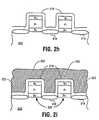
- a control gate material 220is blanket deposited onto the charge storage medium 218 over and around strips 208 .
- the control gate materialis formed to a thickness at least sufficient to completely fill the gaps between adjacent strips.
- a conformal filmdeposited to a thickness of at least one-half the width of the gap while insuring complete filling of the gaps.
- the control gate material 220is a blanket deposited N+ doped polysilicon film formed by chemical vapor deposition.
- the control gatecan be formed from a blanket deposited tungsten film formed by chemical vapor deposition utilizing WF 6 .
- control gate film 220is planarized back, by for example, chemical mechanical polishing until the top surface of the control gate is substantially planar with the charge storage medium on top of strips 208 .
- a plasma etch processis then utilized to recess 222 the top surface of the control gate material 220 below the top surface of strips 208 and preferably to slightly above the junction between N+ region 206 and P region 204 .
- a pair of control gates 224have been formed along laterally opposite sidewalls 210 of strips 208 . The above process forms control gates 224 adjacent to strips 208 in a self aligned manner.
- an interlayer dielectric (ILD) 226such as an oxide, is blanket deposited over the top of strips 208 and over the control gates 224 formed between adjacent strips.
- ILDinterlayer dielectric
- the deposited oxide as well as the charge storage medium on the top of strips 208are polished or etched back with well-known techniques such as chemical mechanical polishing to reveal and open the top surface of N+ region 206 .
- the remaining oxide 226 on the control gates 224provides isolation of control gates 224 from subsequently formed control gates and source/drain conductors.
- Interlayer dielectric 226is formed to a thickness sufficient to completely fill recess 222 .
- a conductive layer 228is blanket deposited onto ILD 226 and N+ region 206 of strips 208 as shown in FIG. 2 m .
- the conductive filmis a highly doped (1 ⁇ 10 19 to 1 ⁇ 10 20 atoms/cm 3 ) N+ polycrystalline silicon film.
- a N+ polycrystalline silicon filmcan be formed by well-known techniques such as by chemical vapor deposition.
- conductive film 228can be a metal conductor such as, but not limited to, tungsten or titanium silicide.
- a N+ polycrystalline silicon film 228can be formed to a thickness between 1000-5000 ⁇ .
- the conductive film 228is patterned into a plurality of conductor lines 230 which run perpendicular or orthogonal to strip 208 .
- Well-known photolithography and etching techniquescan be used to pattern conductive film 228 into a plurality of parallel conductor lines 230 .
- the etch used to pattern conductor lines 230is continued to remove the portion 232 of strip 208 not covered or masked by conductor lines 230 .
- the etchis continued through the top N+ silicon region 206 , and through the P ⁇ silicon region 204 and stops on or in the N+ region 202 . In this way, as shown in FIG.
- square or rectangular pillars 233are formed from the strips or lines 208 at the intersection or overlap of the lines 208 and the conductors 230 .
- square shaped pillars having a width of less than 0.18 ⁇ mare formed.
- the etch steppreferably uses an etch which can selectively etch strip 208 with respect to ILD 226 and charge trapping dielectric 218 .
- siliconcan be anisotropically etched utilizing a plasma etch which utilizes CO 2 and HBr without significantly etching in the oxide ILD 226 .
- ILD 226protects and isolates the underlying control gate 224 .
- N+ region 202is left unetched and provides a conductor (wordline or bitline) which couples pillars 233 together in rows or columns.
- conductor lines 230provide a conductor (bitline or wordline) which couples pillars together in columns or rows.
- the substratecan be subjected to successive ion implantation steps to alter the doping density of each newly revealed surface or face of P type body 204 of pillar 233 in order to alter the doping density of each newly revealed face and therefore the threshold voltage of each face.
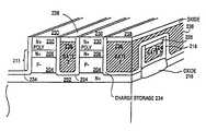
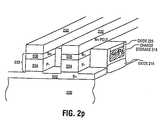
- FIG. 2 pis an isometric view after the etch which forms pillars 233 .
- a second charge storage medium 234is blanket deposited over and around conductors 230 as well as pillars 233 and onto N+ region 202 and oxide dielectric 226 .
- a second control gate material 236is then blanket deposited over and onto second charge storage medium 234 .
- the second control gate materialis then polished back and optionally recessed as described with respect to FIG. 2 j to form a second pair of control gates adjacent to laterally opposites sides of pillars 233 .
- a second interlayer dielectric 238can then be blanket deposited and polished back as described with respect to FIGS. 2 k and 2 l to complete fabrication of the multibit nonvolatile memory device of the present invention.
- each pillar 233has four faces whereby two laterally opposite faces have a charge storage medium 234 and independently controllable control gates 236 while the other laterally opposite faces have a charge storage medium 218 and independently controllable control gates 224 .
- the multibit nonvolatile pillar memory device of the present inventionis complete.
- additional levels of multibit nonvolatile memory devicescan be fabricated with the technique described above.
- conductor 230can be formed of material such as cobalt silicide or titanium silicide which closely matches the lattice structure of single crystalline silicon and therefore can be used as a source for the over growth of single crystal silicon over ILD 238 .
- a multigate transistor having a vertical channel currentis fabricated. That is, although the present invention has been described with respect to the formation of a nonvolatile memory device having a pillar with multiple faces and multiple charge storage mediums and multiple independently controlled gates, the same concepts and fabrication techniques can be used to fabricate NMOS or PMOS transistors having multiple gate electrodes and vertical channel currents. The structure and process of fabrication of a multigate MOS transistor with vertical channel current is the same as memory device 100 as shown in FIGS.
- a gate dielectricis instead formed between each face 110 - 113 of pillar 102 and control gates 118 - 121 which are the gates of the transistor.
- Any well-known and suitable gate dielectriccan be used such as but not limited silicon dioxide and silicon oxynitride.
- the gate dielectricwill typically have a thickness between 10-50 ⁇ .
- the fabricated MOS transistor having multiple gates and vertical read currentshas a first source/drain region, a body or channel region, and a second source/drain region each substantially vertically aligned with one another.
- Each independently controlled gatewould then prevent or allow a channel current to flow in its associated face of the pillar.
- a channel currentflows between the first and second source/drain region through a face of pillar 102 , the channel current flows in a direction perpendicular (z) to the plane (x-y) of the single crystalline substrate on or in which the device is formed.
- Such a devicecan be used to form any type of logic device such as a microprocessor or a programmable logic array (PLA).
- PPAprogrammable logic array
- the use of multiple gates surrounding a vertical structureenables high density integration of MOS devices. Additionally, because multiple gates are formed around a pillar having single source and a single drain region, the MOS device is ideally suited for dynamic or “domino” logic schemes.
Landscapes
- Non-Volatile Memory (AREA)
- Semiconductor Memories (AREA)
Abstract
Description
Claims (28)
Priority Applications (1)
| Application Number | Priority Date | Filing Date | Title |
|---|---|---|---|
| US10/254,878US6677204B2 (en) | 2000-08-14 | 2002-09-26 | Multigate semiconductor device with vertical channel current and method of fabrication |
Applications Claiming Priority (2)
| Application Number | Priority Date | Filing Date | Title |
|---|---|---|---|
| US09/639,577US6580124B1 (en) | 2000-08-14 | 2000-08-14 | Multigate semiconductor device with vertical channel current and method of fabrication |
| US10/254,878US6677204B2 (en) | 2000-08-14 | 2002-09-26 | Multigate semiconductor device with vertical channel current and method of fabrication |
Related Parent Applications (1)
| Application Number | Title | Priority Date | Filing Date |
|---|---|---|---|
| US09/639,577DivisionUS6580124B1 (en) | 2000-08-14 | 2000-08-14 | Multigate semiconductor device with vertical channel current and method of fabrication |
Publications (2)
| Publication Number | Publication Date |
|---|---|
| US20030139011A1 US20030139011A1 (en) | 2003-07-24 |
| US6677204B2true US6677204B2 (en) | 2004-01-13 |
Family
ID=24564683
Family Applications (2)
| Application Number | Title | Priority Date | Filing Date |
|---|---|---|---|
| US09/639,577Expired - LifetimeUS6580124B1 (en) | 2000-08-14 | 2000-08-14 | Multigate semiconductor device with vertical channel current and method of fabrication |
| US10/254,878Expired - Fee RelatedUS6677204B2 (en) | 2000-08-14 | 2002-09-26 | Multigate semiconductor device with vertical channel current and method of fabrication |
Family Applications Before (1)
| Application Number | Title | Priority Date | Filing Date |
|---|---|---|---|
| US09/639,577Expired - LifetimeUS6580124B1 (en) | 2000-08-14 | 2000-08-14 | Multigate semiconductor device with vertical channel current and method of fabrication |
Country Status (4)
| Country | Link |
|---|---|
| US (2) | US6580124B1 (en) |
| AU (1) | AU2001291257A1 (en) |
| TW (1) | TW505998B (en) |
| WO (1) | WO2002015278A2 (en) |
Cited By (271)
| Publication number | Priority date | Publication date | Assignee | Title |
|---|---|---|---|---|
| US20020100011A1 (en)* | 2001-01-19 | 2002-07-25 | Chang Yao Wen | NROM structure |
| US20040110390A1 (en)* | 2002-12-06 | 2004-06-10 | Fasl Llc | Semiconductor memory device and method of fabricating the same |
| US20040124415A1 (en)* | 2002-12-31 | 2004-07-01 | Walker Andrew J. | Formation of thin channels for TFT devices to ensure low variability of threshold voltages |
| US20050023584A1 (en)* | 2002-05-02 | 2005-02-03 | Micron Technology, Inc. | Atomic layer deposition and conversion |
| US20050105341A1 (en)* | 2003-11-04 | 2005-05-19 | Micron Technology, Inc. | NROM flash memory with self-aligned structural charge separation |
| US20050124170A1 (en)* | 2003-12-05 | 2005-06-09 | Advanced Micro Devices, Inc. | Strained semiconductor substrate and processes therefor |
| US20050280156A1 (en)* | 2004-06-21 | 2005-12-22 | Sang-Yun Lee | Semiconductor device with base support structure |
| US20050280155A1 (en)* | 2004-06-21 | 2005-12-22 | Sang-Yun Lee | Semiconductor bonding and layer transfer method |
| US20060141558A1 (en)* | 2004-12-29 | 2006-06-29 | Xiao-Song Tang | Bioproduction of astaxanthin using mutant carotenoid ketolase and carotenoid hydroxylase genes |
| KR100634260B1 (en) | 2005-07-29 | 2006-10-13 | 삼성전자주식회사 | Thin film formation method and semiconductor device formation method using the same |
| US20070018229A1 (en)* | 2005-07-25 | 2007-01-25 | Freescale Semiconductor, Inc. | Electronic device including discontinuous storage elements and a process for forming the same |
| US20070020845A1 (en)* | 2005-07-25 | 2007-01-25 | Freescale Semiconductor, Inc. | Method of fabricating programmable structure including discontinuous storage elements and spacer control gates in a trench |
| US20070018222A1 (en)* | 2005-07-25 | 2007-01-25 | Freescale Semiconductor, Inc. | Electronic device including discontinuous storage elements |
| US20070018221A1 (en)* | 2005-07-25 | 2007-01-25 | Freescale Semiconductor, Inc. | Programmable structure including discontinuous storage elements and spacer control gates in a trench |
| US20070020856A1 (en)* | 2005-07-25 | 2007-01-25 | Freescale Semiconductor, Inc. | Process for forming an electronic device including discontinuous storage elements |
| US20070019472A1 (en)* | 2005-07-25 | 2007-01-25 | Freescale Semiconductor, Inc. | Electronic device including a memory array and conductive lines |
| US20070020851A1 (en)* | 2005-07-25 | 2007-01-25 | Freescale Semiconductor, Inc. | Hot carrier injection programmable structure including discontinuous storage elements and spacer control gates in a trench and a method of using the same |
| US20070020840A1 (en)* | 2005-07-25 | 2007-01-25 | Freescale Semiconductor, Inc. | Programmable structure including nanocrystal storage elements in a trench |
| US20070018232A1 (en)* | 2005-07-25 | 2007-01-25 | Freescale Semiconductor, Inc. | Nonvolatile storage array with continuous control gate employing hot carrier injection programming |
| US20070018234A1 (en)* | 2005-07-25 | 2007-01-25 | Freescale Semiconductor, Inc. | Electronic device including gate lines, bit lines, or a combination thereof |
| US20070018216A1 (en)* | 2005-07-25 | 2007-01-25 | Freescale Semiconductor, Inc. | Electronic device including discontinuous storage elements |
| US20070020831A1 (en)* | 2005-07-25 | 2007-01-25 | Freescale Semiconductor, Inc. | Method of fabricating a nonvolatile storage array with continuous control gate employing hot carrier injection programming |
| US20070057309A1 (en)* | 2005-09-15 | 2007-03-15 | Samsung Electronics Co., Ltd. | Nonvolatile semiconductor memory devices and methods of forming the same |
| US20070092989A1 (en)* | 2005-08-04 | 2007-04-26 | Micron Technology, Inc. | Conductive nanoparticles |
| US7262104B1 (en)* | 2004-06-02 | 2007-08-28 | Advanced Micro Devices, Inc. | Selective channel implantation for forming semiconductor devices with different threshold voltages |
| US7399675B2 (en) | 2004-10-08 | 2008-07-15 | Freescale Semiconductor, Inc | Electronic device including an array and process for forming the same |
| US20080173922A1 (en)* | 2007-01-24 | 2008-07-24 | Freescale Semiconductor, Inc. | Electronic device including fins and discontinuous storage elements and processes of forming and using the same |
| US20080173923A1 (en)* | 2007-01-24 | 2008-07-24 | Freescale Semiconductor, Inc. | Electronic device including trenches and discontinuous storage elements and processes of forming and using the same |
| US20080173921A1 (en)* | 2007-01-24 | 2008-07-24 | Freescale Semiconductor, Inc. | Electronic device including trenches and discontinuous storage elements and processes of forming and using the same |
| US20080296650A1 (en)* | 2007-06-04 | 2008-12-04 | Micron Technology, Inc. | High-k dielectrics with gold nano-particles |
| US20090111241A1 (en)* | 2003-06-24 | 2009-04-30 | Sang-Yun Lee | Wafer bonding method |
| US20090173991A1 (en)* | 2005-08-04 | 2009-07-09 | Marsh Eugene P | Methods for forming rhodium-based charge traps and apparatus including rhodium-based charge traps |
| US20090224364A1 (en)* | 2003-06-24 | 2009-09-10 | Oh Choonsik | Semiconductor circuit and method of fabricating the same |
| US7592224B2 (en) | 2006-03-30 | 2009-09-22 | Freescale Semiconductor, Inc | Method of fabricating a storage device including decontinuous storage elements within and between trenches |
| US20090325343A1 (en)* | 2003-06-24 | 2009-12-31 | Sang-Yun Lee | Bonded semiconductor structure and method of fabricating the same |
| US20100006919A1 (en)* | 2008-07-11 | 2010-01-14 | Samsung Electronics Co., Ltd. | Non-volatile memory device and method of fabrication |
| US20100038743A1 (en)* | 2003-06-24 | 2010-02-18 | Sang-Yun Lee | Information storage system which includes a bonded semiconductor structure |
| US20100133695A1 (en)* | 2003-01-12 | 2010-06-03 | Sang-Yun Lee | Electronic circuit with embedded memory |
| US20100190334A1 (en)* | 2003-06-24 | 2010-07-29 | Sang-Yun Lee | Three-dimensional semiconductor structure and method of manufacturing the same |
| US20100295120A1 (en)* | 2009-05-20 | 2010-11-25 | Gurtej Sandhu | Vertically-oriented semiconductor selection device providing high drive current in cross-point array memory |
| US20110003438A1 (en)* | 2005-03-29 | 2011-01-06 | Sang-Yun Lee | Three-dimensional integrated circuit structure |
| US7867822B2 (en) | 2003-06-24 | 2011-01-11 | Sang-Yun Lee | Semiconductor memory device |
| US20110037497A1 (en)* | 2009-04-14 | 2011-02-17 | Or-Ment Llc | Method for Fabrication of a Semiconductor Device and Structure |
| US20110049577A1 (en)* | 2009-04-14 | 2011-03-03 | NuPGA Corporation | System comprising a semiconductor device and structure |
| US20110053332A1 (en)* | 2003-06-24 | 2011-03-03 | Sang-Yun Lee | Semiconductor circuit |
| US20110084314A1 (en)* | 2009-10-12 | 2011-04-14 | NuPGA Corporation | System comprising a semiconductor device and structure |
| US7927948B2 (en) | 2005-07-20 | 2011-04-19 | Micron Technology, Inc. | Devices with nanocrystals and methods of formation |
| US20110092030A1 (en)* | 2009-04-14 | 2011-04-21 | NuPGA Corporation | System comprising a semiconductor device and structure |
| US20110108888A1 (en)* | 2009-04-14 | 2011-05-12 | NuPGA Corporation | System comprising a semiconductor device and structure |
| US20110121366A1 (en)* | 2009-04-14 | 2011-05-26 | NuPGA Corporation | System comprising a semiconductor device and structure |
| US20110143506A1 (en)* | 2009-12-10 | 2011-06-16 | Sang-Yun Lee | Method for fabricating a semiconductor memory device |
| US8058142B2 (en) | 1996-11-04 | 2011-11-15 | Besang Inc. | Bonded semiconductor structure and method of making the same |
| US20120061639A1 (en)* | 2010-09-14 | 2012-03-15 | Naoki Yasuda | Resistance change memory |
| US20120120728A1 (en)* | 2010-11-16 | 2012-05-17 | Samsung Electronics Co., Ltd | Non-volatile memory device |
| US8203148B2 (en) | 2010-10-11 | 2012-06-19 | Monolithic 3D Inc. | Semiconductor device and structure |
| US20120217619A1 (en)* | 2011-02-28 | 2012-08-30 | Min-Soo Kim | Semiconductor device with triangle prism pillar and method for manufacturing the same |
| US8273610B2 (en) | 2010-11-18 | 2012-09-25 | Monolithic 3D Inc. | Method of constructing a semiconductor device and structure |
| US8294159B2 (en) | 2009-10-12 | 2012-10-23 | Monolithic 3D Inc. | Method for fabrication of a semiconductor device and structure |
| US8362800B2 (en) | 2010-10-13 | 2013-01-29 | Monolithic 3D Inc. | 3D semiconductor device including field repairable logics |
| US8373439B2 (en) | 2009-04-14 | 2013-02-12 | Monolithic 3D Inc. | 3D semiconductor device |
| US8373230B1 (en) | 2010-10-13 | 2013-02-12 | Monolithic 3D Inc. | Method for fabrication of a semiconductor device and structure |
| US8378494B2 (en) | 2009-04-14 | 2013-02-19 | Monolithic 3D Inc. | Method for fabrication of a semiconductor device and structure |
| US8379458B1 (en) | 2010-10-13 | 2013-02-19 | Monolithic 3D Inc. | Semiconductor device and structure |
| US8378715B2 (en) | 2009-04-14 | 2013-02-19 | Monolithic 3D Inc. | Method to construct systems |
| US8427200B2 (en) | 2009-04-14 | 2013-04-23 | Monolithic 3D Inc. | 3D semiconductor device |
| US8440542B2 (en) | 2010-10-11 | 2013-05-14 | Monolithic 3D Inc. | Semiconductor device and structure |
| US8450804B2 (en) | 2011-03-06 | 2013-05-28 | Monolithic 3D Inc. | Semiconductor device and structure for heat removal |
| US8455978B2 (en) | 2010-05-27 | 2013-06-04 | Sang-Yun Lee | Semiconductor circuit structure and method of making the same |
| US8461035B1 (en) | 2010-09-30 | 2013-06-11 | Monolithic 3D Inc. | Method for fabrication of a semiconductor device and structure |
| US8476145B2 (en) | 2010-10-13 | 2013-07-02 | Monolithic 3D Inc. | Method of fabricating a semiconductor device and structure |
| US8492886B2 (en) | 2010-02-16 | 2013-07-23 | Monolithic 3D Inc | 3D integrated circuit with logic |
| US8536023B2 (en) | 2010-11-22 | 2013-09-17 | Monolithic 3D Inc. | Method of manufacturing a semiconductor device and structure |
| US8541819B1 (en) | 2010-12-09 | 2013-09-24 | Monolithic 3D Inc. | Semiconductor device and structure |
| US8557632B1 (en) | 2012-04-09 | 2013-10-15 | Monolithic 3D Inc. | Method for fabrication of a semiconductor device and structure |
| US8574929B1 (en) | 2012-11-16 | 2013-11-05 | Monolithic 3D Inc. | Method to form a 3D semiconductor device and structure |
| US8581349B1 (en) | 2011-05-02 | 2013-11-12 | Monolithic 3D Inc. | 3D memory semiconductor device and structure |
| US8642416B2 (en) | 2010-07-30 | 2014-02-04 | Monolithic 3D Inc. | Method of forming three dimensional integrated circuit devices using layer transfer technique |
| US8669778B1 (en) | 2009-04-14 | 2014-03-11 | Monolithic 3D Inc. | Method for design and manufacturing of a 3D semiconductor device |
| US8674470B1 (en) | 2012-12-22 | 2014-03-18 | Monolithic 3D Inc. | Semiconductor device and structure |
| US8687399B2 (en) | 2011-10-02 | 2014-04-01 | Monolithic 3D Inc. | Semiconductor device and structure |
| US8686428B1 (en) | 2012-11-16 | 2014-04-01 | Monolithic 3D Inc. | Semiconductor device and structure |
| US8709880B2 (en) | 2010-07-30 | 2014-04-29 | Monolithic 3D Inc | Method for fabrication of a semiconductor device and structure |
| US8723335B2 (en) | 2010-05-20 | 2014-05-13 | Sang-Yun Lee | Semiconductor circuit structure and method of forming the same using a capping layer |
| US8742476B1 (en) | 2012-11-27 | 2014-06-03 | Monolithic 3D Inc. | Semiconductor device and structure |
| US8753913B2 (en) | 2010-10-13 | 2014-06-17 | Monolithic 3D Inc. | Method for fabricating novel semiconductor and optoelectronic devices |
| US8803206B1 (en) | 2012-12-29 | 2014-08-12 | Monolithic 3D Inc. | 3D semiconductor device and structure |
| US8902663B1 (en) | 2013-03-11 | 2014-12-02 | Monolithic 3D Inc. | Method of maintaining a memory state |
| US8901613B2 (en) | 2011-03-06 | 2014-12-02 | Monolithic 3D Inc. | Semiconductor device and structure for heat removal |
| US8975670B2 (en) | 2011-03-06 | 2015-03-10 | Monolithic 3D Inc. | Semiconductor device and structure for heat removal |
| US8994404B1 (en) | 2013-03-12 | 2015-03-31 | Monolithic 3D Inc. | Semiconductor device and structure |
| US9000557B2 (en) | 2012-03-17 | 2015-04-07 | Zvi Or-Bach | Semiconductor device and structure |
| US9029173B2 (en) | 2011-10-18 | 2015-05-12 | Monolithic 3D Inc. | Method for fabrication of a semiconductor device and structure |
| US20150206886A1 (en)* | 2012-08-21 | 2015-07-23 | Micron Technology, Inc. | Methods of Forming Memory Arrays and Semiconductor Constructions |
| US9099424B1 (en) | 2012-08-10 | 2015-08-04 | Monolithic 3D Inc. | Semiconductor system, device and structure with heat removal |
| US9099526B2 (en) | 2010-02-16 | 2015-08-04 | Monolithic 3D Inc. | Integrated circuit device and structure |
| US9117749B1 (en) | 2013-03-15 | 2015-08-25 | Monolithic 3D Inc. | Semiconductor device and structure |
| US9197804B1 (en) | 2011-10-14 | 2015-11-24 | Monolithic 3D Inc. | Semiconductor and optoelectronic devices |
| US9214529B2 (en) | 2011-03-14 | 2015-12-15 | Globalfoundries Inc. | Fin Fet device with independent control gate |
| US9219005B2 (en) | 2011-06-28 | 2015-12-22 | Monolithic 3D Inc. | Semiconductor system and device |
| US9509313B2 (en) | 2009-04-14 | 2016-11-29 | Monolithic 3D Inc. | 3D semiconductor device |
| US9577642B2 (en) | 2009-04-14 | 2017-02-21 | Monolithic 3D Inc. | Method to form a 3D semiconductor device |
| US9871034B1 (en) | 2012-12-29 | 2018-01-16 | Monolithic 3D Inc. | Semiconductor device and structure |
| US9953925B2 (en) | 2011-06-28 | 2018-04-24 | Monolithic 3D Inc. | Semiconductor system and device |
| US10043781B2 (en) | 2009-10-12 | 2018-08-07 | Monolithic 3D Inc. | 3D semiconductor device and structure |
| US10115663B2 (en) | 2012-12-29 | 2018-10-30 | Monolithic 3D Inc. | 3D semiconductor device and structure |
| US10127344B2 (en) | 2013-04-15 | 2018-11-13 | Monolithic 3D Inc. | Automation for monolithic 3D devices |
| US10157909B2 (en) | 2009-10-12 | 2018-12-18 | Monolithic 3D Inc. | 3D semiconductor device and structure |
| US10217667B2 (en) | 2011-06-28 | 2019-02-26 | Monolithic 3D Inc. | 3D semiconductor device, fabrication method and system |
| US10224279B2 (en) | 2013-03-15 | 2019-03-05 | Monolithic 3D Inc. | Semiconductor device and structure |
| US10290682B2 (en) | 2010-10-11 | 2019-05-14 | Monolithic 3D Inc. | 3D IC semiconductor device and structure with stacked memory |
| US10297586B2 (en) | 2015-03-09 | 2019-05-21 | Monolithic 3D Inc. | Methods for processing a 3D semiconductor device |
| US10325651B2 (en) | 2013-03-11 | 2019-06-18 | Monolithic 3D Inc. | 3D semiconductor device with stacked memory |
| US10354995B2 (en) | 2009-10-12 | 2019-07-16 | Monolithic 3D Inc. | Semiconductor memory device and structure |
| US10366970B2 (en) | 2009-10-12 | 2019-07-30 | Monolithic 3D Inc. | 3D semiconductor device and structure |
| US10381328B2 (en) | 2015-04-19 | 2019-08-13 | Monolithic 3D Inc. | Semiconductor device and structure |
| US10388568B2 (en) | 2011-06-28 | 2019-08-20 | Monolithic 3D Inc. | 3D semiconductor device and system |
| US10388863B2 (en) | 2009-10-12 | 2019-08-20 | Monolithic 3D Inc. | 3D memory device and structure |
| US10418369B2 (en) | 2015-10-24 | 2019-09-17 | Monolithic 3D Inc. | Multi-level semiconductor memory device and structure |
| US10497713B2 (en) | 2010-11-18 | 2019-12-03 | Monolithic 3D Inc. | 3D semiconductor memory device and structure |
| US10515981B2 (en) | 2015-09-21 | 2019-12-24 | Monolithic 3D Inc. | Multilevel semiconductor device and structure with memory |
| US10522225B1 (en) | 2015-10-02 | 2019-12-31 | Monolithic 3D Inc. | Semiconductor device with non-volatile memory |
| US10600888B2 (en) | 2012-04-09 | 2020-03-24 | Monolithic 3D Inc. | 3D semiconductor device |
| US10600657B2 (en) | 2012-12-29 | 2020-03-24 | Monolithic 3D Inc | 3D semiconductor device and structure |
| US10651054B2 (en) | 2012-12-29 | 2020-05-12 | Monolithic 3D Inc. | 3D semiconductor device and structure |
| US10679977B2 (en) | 2010-10-13 | 2020-06-09 | Monolithic 3D Inc. | 3D microdisplay device and structure |
| US10825779B2 (en) | 2015-04-19 | 2020-11-03 | Monolithic 3D Inc. | 3D semiconductor device and structure |
| US10833108B2 (en) | 2010-10-13 | 2020-11-10 | Monolithic 3D Inc. | 3D microdisplay device and structure |
| US10840239B2 (en) | 2014-08-26 | 2020-11-17 | Monolithic 3D Inc. | 3D semiconductor device and structure |
| US10847540B2 (en) | 2015-10-24 | 2020-11-24 | Monolithic 3D Inc. | 3D semiconductor memory device and structure |
| US10892016B1 (en) | 2019-04-08 | 2021-01-12 | Monolithic 3D Inc. | 3D memory semiconductor devices and structures |
| US10892169B2 (en) | 2012-12-29 | 2021-01-12 | Monolithic 3D Inc. | 3D semiconductor device and structure |
| US10896931B1 (en) | 2010-10-11 | 2021-01-19 | Monolithic 3D Inc. | 3D semiconductor device and structure |
| US10903089B1 (en) | 2012-12-29 | 2021-01-26 | Monolithic 3D Inc. | 3D semiconductor device and structure |
| US10910364B2 (en) | 2009-10-12 | 2021-02-02 | Monolitaic 3D Inc. | 3D semiconductor device |
| US10943934B2 (en) | 2010-10-13 | 2021-03-09 | Monolithic 3D Inc. | Multilevel semiconductor device and structure |
| US10978501B1 (en) | 2010-10-13 | 2021-04-13 | Monolithic 3D Inc. | Multilevel semiconductor device and structure with waveguides |
| US10998374B1 (en) | 2010-10-13 | 2021-05-04 | Monolithic 3D Inc. | Multilevel semiconductor device and structure |
| US11004694B1 (en) | 2012-12-29 | 2021-05-11 | Monolithic 3D Inc. | 3D semiconductor device and structure |
| US11004719B1 (en) | 2010-11-18 | 2021-05-11 | Monolithic 3D Inc. | Methods for producing a 3D semiconductor memory device and structure |
| US11011507B1 (en) | 2015-04-19 | 2021-05-18 | Monolithic 3D Inc. | 3D semiconductor device and structure |
| US11018156B2 (en) | 2019-04-08 | 2021-05-25 | Monolithic 3D Inc. | 3D memory semiconductor devices and structures |
| US11018116B2 (en) | 2012-12-22 | 2021-05-25 | Monolithic 3D Inc. | Method to form a 3D semiconductor device and structure |
| US11018042B1 (en) | 2010-11-18 | 2021-05-25 | Monolithic 3D Inc. | 3D semiconductor memory device and structure |
| US11018133B2 (en) | 2009-10-12 | 2021-05-25 | Monolithic 3D Inc. | 3D integrated circuit |
| US11018191B1 (en) | 2010-10-11 | 2021-05-25 | Monolithic 3D Inc. | 3D semiconductor device and structure |
| US11024673B1 (en) | 2010-10-11 | 2021-06-01 | Monolithic 3D Inc. | 3D semiconductor device and structure |
| US11030371B2 (en) | 2013-04-15 | 2021-06-08 | Monolithic 3D Inc. | Automation for monolithic 3D devices |
| US11031394B1 (en) | 2014-01-28 | 2021-06-08 | Monolithic 3D Inc. | 3D semiconductor device and structure |
| US11031275B2 (en) | 2010-11-18 | 2021-06-08 | Monolithic 3D Inc. | 3D semiconductor device and structure with memory |
| US11043523B1 (en) | 2010-10-13 | 2021-06-22 | Monolithic 3D Inc. | Multilevel semiconductor device and structure with image sensors |
| US11056468B1 (en) | 2015-04-19 | 2021-07-06 | Monolithic 3D Inc. | 3D semiconductor device and structure |
| US11063024B1 (en) | 2012-12-22 | 2021-07-13 | Monlithic 3D Inc. | Method to form a 3D semiconductor device and structure |
| US11063071B1 (en) | 2010-10-13 | 2021-07-13 | Monolithic 3D Inc. | Multilevel semiconductor device and structure with waveguides |
| US11088050B2 (en) | 2012-04-09 | 2021-08-10 | Monolithic 3D Inc. | 3D semiconductor device with isolation layers |
| US11088130B2 (en) | 2014-01-28 | 2021-08-10 | Monolithic 3D Inc. | 3D semiconductor device and structure |
| US11087995B1 (en) | 2012-12-29 | 2021-08-10 | Monolithic 3D Inc. | 3D semiconductor device and structure |
| US11094576B1 (en) | 2010-11-18 | 2021-08-17 | Monolithic 3D Inc. | Methods for producing a 3D semiconductor memory device and structure |
| US11107721B2 (en) | 2010-11-18 | 2021-08-31 | Monolithic 3D Inc. | 3D semiconductor device and structure with NAND logic |
| US11107808B1 (en) | 2014-01-28 | 2021-08-31 | Monolithic 3D Inc. | 3D semiconductor device and structure |
| US11114464B2 (en) | 2015-10-24 | 2021-09-07 | Monolithic 3D Inc. | 3D semiconductor device and structure |
| US11114427B2 (en) | 2015-11-07 | 2021-09-07 | Monolithic 3D Inc. | 3D semiconductor processor and memory device and structure |
| US11121021B2 (en) | 2010-11-18 | 2021-09-14 | Monolithic 3D Inc. | 3D semiconductor device and structure |
| US11133344B2 (en) | 2010-10-13 | 2021-09-28 | Monolithic 3D Inc. | Multilevel semiconductor device and structure with image sensors |
| US11158674B2 (en) | 2010-10-11 | 2021-10-26 | Monolithic 3D Inc. | Method to produce a 3D semiconductor device and structure |
| US11158652B1 (en) | 2019-04-08 | 2021-10-26 | Monolithic 3D Inc. | 3D memory semiconductor devices and structures |
| US11164811B2 (en) | 2012-04-09 | 2021-11-02 | Monolithic 3D Inc. | 3D semiconductor device with isolation layers and oxide-to-oxide bonding |
| US11163112B2 (en) | 2010-10-13 | 2021-11-02 | Monolithic 3D Inc. | Multilevel semiconductor device and structure with electromagnetic modulators |
| US11164770B1 (en) | 2010-11-18 | 2021-11-02 | Monolithic 3D Inc. | Method for producing a 3D semiconductor memory device and structure |
| US11164898B2 (en) | 2010-10-13 | 2021-11-02 | Monolithic 3D Inc. | Multilevel semiconductor device and structure |
| US11177140B2 (en) | 2012-12-29 | 2021-11-16 | Monolithic 3D Inc. | 3D semiconductor device and structure |
| US11211279B2 (en) | 2010-11-18 | 2021-12-28 | Monolithic 3D Inc. | Method for processing a 3D integrated circuit and structure |
| US11217565B2 (en) | 2012-12-22 | 2022-01-04 | Monolithic 3D Inc. | Method to form a 3D semiconductor device and structure |
| US11227897B2 (en) | 2010-10-11 | 2022-01-18 | Monolithic 3D Inc. | Method for producing a 3D semiconductor memory device and structure |
| US11251149B2 (en) | 2016-10-10 | 2022-02-15 | Monolithic 3D Inc. | 3D memory device and structure |
| US11257867B1 (en) | 2010-10-11 | 2022-02-22 | Monolithic 3D Inc. | 3D semiconductor device and structure with oxide bonds |
| US11270055B1 (en) | 2013-04-15 | 2022-03-08 | Monolithic 3D Inc. | Automation for monolithic 3D devices |
| US11296106B2 (en) | 2019-04-08 | 2022-04-05 | Monolithic 3D Inc. | 3D memory semiconductor devices and structures |
| US11296115B1 (en) | 2015-10-24 | 2022-04-05 | Monolithic 3D Inc. | 3D semiconductor device and structure |
| US11309292B2 (en) | 2012-12-22 | 2022-04-19 | Monolithic 3D Inc. | 3D semiconductor device and structure with metal layers |
| US11315980B1 (en) | 2010-10-11 | 2022-04-26 | Monolithic 3D Inc. | 3D semiconductor device and structure with transistors |
| US11329059B1 (en) | 2016-10-10 | 2022-05-10 | Monolithic 3D Inc. | 3D memory devices and structures with thinned single crystal substrates |
| US11327227B2 (en) | 2010-10-13 | 2022-05-10 | Monolithic 3D Inc. | Multilevel semiconductor device and structure with electromagnetic modulators |
| US11341309B1 (en) | 2013-04-15 | 2022-05-24 | Monolithic 3D Inc. | Automation for monolithic 3D devices |
| US11355381B2 (en) | 2010-11-18 | 2022-06-07 | Monolithic 3D Inc. | 3D semiconductor memory device and structure |
| US11355380B2 (en) | 2010-11-18 | 2022-06-07 | Monolithic 3D Inc. | Methods for producing 3D semiconductor memory device and structure utilizing alignment marks |
| US11374118B2 (en) | 2009-10-12 | 2022-06-28 | Monolithic 3D Inc. | Method to form a 3D integrated circuit |
| US11398569B2 (en) | 2013-03-12 | 2022-07-26 | Monolithic 3D Inc. | 3D semiconductor device and structure |
| US11404466B2 (en) | 2010-10-13 | 2022-08-02 | Monolithic 3D Inc. | Multilevel semiconductor device and structure with image sensors |
| US11410912B2 (en) | 2012-04-09 | 2022-08-09 | Monolithic 3D Inc. | 3D semiconductor device with vias and isolation layers |
| US11430668B2 (en) | 2012-12-29 | 2022-08-30 | Monolithic 3D Inc. | 3D semiconductor device and structure with bonding |
| US11430667B2 (en) | 2012-12-29 | 2022-08-30 | Monolithic 3D Inc. | 3D semiconductor device and structure with bonding |
| US11437368B2 (en) | 2010-10-13 | 2022-09-06 | Monolithic 3D Inc. | Multilevel semiconductor device and structure with oxide bonding |
| US11443971B2 (en) | 2010-11-18 | 2022-09-13 | Monolithic 3D Inc. | 3D semiconductor device and structure with memory |
| US11469271B2 (en) | 2010-10-11 | 2022-10-11 | Monolithic 3D Inc. | Method to produce 3D semiconductor devices and structures with memory |
| US11476181B1 (en) | 2012-04-09 | 2022-10-18 | Monolithic 3D Inc. | 3D semiconductor device and structure with metal layers |
| US11482440B2 (en) | 2010-12-16 | 2022-10-25 | Monolithic 3D Inc. | 3D semiconductor device and structure with a built-in test circuit for repairing faulty circuits |
| US11482438B2 (en) | 2010-11-18 | 2022-10-25 | Monolithic 3D Inc. | Methods for producing a 3D semiconductor memory device and structure |
| US11482439B2 (en) | 2010-11-18 | 2022-10-25 | Monolithic 3D Inc. | Methods for producing a 3D semiconductor memory device comprising charge trap junction-less transistors |
| US11487928B2 (en) | 2013-04-15 | 2022-11-01 | Monolithic 3D Inc. | Automation for monolithic 3D devices |
| US11495484B2 (en) | 2010-11-18 | 2022-11-08 | Monolithic 3D Inc. | 3D semiconductor devices and structures with at least two single-crystal layers |
| US11508605B2 (en) | 2010-11-18 | 2022-11-22 | Monolithic 3D Inc. | 3D semiconductor memory device and structure |
| US11521888B2 (en) | 2010-11-18 | 2022-12-06 | Monolithic 3D Inc. | 3D semiconductor device and structure with high-k metal gate transistors |
| US11569117B2 (en) | 2010-11-18 | 2023-01-31 | Monolithic 3D Inc. | 3D semiconductor device and structure with single-crystal layers |
| US11574109B1 (en) | 2013-04-15 | 2023-02-07 | Monolithic 3D Inc | Automation methods for 3D integrated circuits and devices |
| US11594473B2 (en) | 2012-04-09 | 2023-02-28 | Monolithic 3D Inc. | 3D semiconductor device and structure with metal layers and a connective path |
| US11600667B1 (en) | 2010-10-11 | 2023-03-07 | Monolithic 3D Inc. | Method to produce 3D semiconductor devices and structures with memory |
| US11605663B2 (en) | 2010-10-13 | 2023-03-14 | Monolithic 3D Inc. | Multilevel semiconductor device and structure with image sensors and wafer bonding |
| US11610802B2 (en) | 2010-11-18 | 2023-03-21 | Monolithic 3D Inc. | Method for producing a 3D semiconductor device and structure with single crystal transistors and metal gate electrodes |
| US11615977B2 (en) | 2010-11-18 | 2023-03-28 | Monolithic 3D Inc. | 3D semiconductor memory device and structure |
| US11616004B1 (en) | 2012-04-09 | 2023-03-28 | Monolithic 3D Inc. | 3D semiconductor device and structure with metal layers and a connective path |
| US11694922B2 (en) | 2010-10-13 | 2023-07-04 | Monolithic 3D Inc. | Multilevel semiconductor device and structure with oxide bonding |
| US11694944B1 (en) | 2012-04-09 | 2023-07-04 | Monolithic 3D Inc. | 3D semiconductor device and structure with metal layers and a connective path |
| US11711928B2 (en) | 2016-10-10 | 2023-07-25 | Monolithic 3D Inc. | 3D memory devices and structures with control circuits |
| US11720736B2 (en) | 2013-04-15 | 2023-08-08 | Monolithic 3D Inc. | Automation methods for 3D integrated circuits and devices |
| US11735501B1 (en) | 2012-04-09 | 2023-08-22 | Monolithic 3D Inc. | 3D semiconductor device and structure with metal layers and a connective path |
| US11735462B2 (en) | 2010-11-18 | 2023-08-22 | Monolithic 3D Inc. | 3D semiconductor device and structure with single-crystal layers |
| US11763864B2 (en) | 2019-04-08 | 2023-09-19 | Monolithic 3D Inc. | 3D memory semiconductor devices and structures with bit-line pillars |
| US11784169B2 (en) | 2012-12-22 | 2023-10-10 | Monolithic 3D Inc. | 3D semiconductor device and structure with metal layers |
| US11784082B2 (en) | 2010-11-18 | 2023-10-10 | Monolithic 3D Inc. | 3D semiconductor device and structure with bonding |
| US11804396B2 (en) | 2010-11-18 | 2023-10-31 | Monolithic 3D Inc. | Methods for producing a 3D semiconductor device and structure with memory cells and multiple metal layers |
| US11812620B2 (en) | 2016-10-10 | 2023-11-07 | Monolithic 3D Inc. | 3D DRAM memory devices and structures with control circuits |
| US11855100B2 (en) | 2010-10-13 | 2023-12-26 | Monolithic 3D Inc. | Multilevel semiconductor device and structure with oxide bonding |
| US11854857B1 (en) | 2010-11-18 | 2023-12-26 | Monolithic 3D Inc. | Methods for producing a 3D semiconductor device and structure with memory cells and multiple metal layers |
| US11855114B2 (en) | 2010-10-13 | 2023-12-26 | Monolithic 3D Inc. | Multilevel semiconductor device and structure with image sensors and wafer bonding |
| US11862503B2 (en) | 2010-11-18 | 2024-01-02 | Monolithic 3D Inc. | Method for producing a 3D semiconductor device and structure with memory cells and multiple metal layers |
| US11869965B2 (en) | 2013-03-11 | 2024-01-09 | Monolithic 3D Inc. | 3D semiconductor device and structure with metal layers and memory cells |
| US11869915B2 (en) | 2010-10-13 | 2024-01-09 | Monolithic 3D Inc. | Multilevel semiconductor device and structure with image sensors and wafer bonding |
| US11869591B2 (en) | 2016-10-10 | 2024-01-09 | Monolithic 3D Inc. | 3D memory devices and structures with control circuits |
| US11881443B2 (en) | 2012-04-09 | 2024-01-23 | Monolithic 3D Inc. | 3D semiconductor device and structure with metal layers and a connective path |
| US11901210B2 (en) | 2010-11-18 | 2024-02-13 | Monolithic 3D Inc. | 3D semiconductor device and structure with memory |
| US11916045B2 (en) | 2012-12-22 | 2024-02-27 | Monolithic 3D Inc. | 3D semiconductor device and structure with metal layers |
| US11923374B2 (en) | 2013-03-12 | 2024-03-05 | Monolithic 3D Inc. | 3D semiconductor device and structure with metal layers |
| US11923230B1 (en) | 2010-11-18 | 2024-03-05 | Monolithic 3D Inc. | 3D semiconductor device and structure with bonding |
| US11930648B1 (en) | 2016-10-10 | 2024-03-12 | Monolithic 3D Inc. | 3D memory devices and structures with metal layers |
| US11929372B2 (en) | 2010-10-13 | 2024-03-12 | Monolithic 3D Inc. | Multilevel semiconductor device and structure with image sensors and wafer bonding |
| US11937422B2 (en) | 2015-11-07 | 2024-03-19 | Monolithic 3D Inc. | Semiconductor memory device and structure |
| US11935949B1 (en) | 2013-03-11 | 2024-03-19 | Monolithic 3D Inc. | 3D semiconductor device and structure with metal layers and memory cells |
| US11956952B2 (en) | 2015-08-23 | 2024-04-09 | Monolithic 3D Inc. | Semiconductor memory device and structure |
| US11961827B1 (en) | 2012-12-22 | 2024-04-16 | Monolithic 3D Inc. | 3D semiconductor device and structure with metal layers |
| US11967583B2 (en) | 2012-12-22 | 2024-04-23 | Monolithic 3D Inc. | 3D semiconductor device and structure with metal layers |
| US11978731B2 (en) | 2015-09-21 | 2024-05-07 | Monolithic 3D Inc. | Method to produce a multi-level semiconductor memory device and structure |
| US11984445B2 (en) | 2009-10-12 | 2024-05-14 | Monolithic 3D Inc. | 3D semiconductor devices and structures with metal layers |
| US11984438B2 (en) | 2010-10-13 | 2024-05-14 | Monolithic 3D Inc. | Multilevel semiconductor device and structure with oxide bonding |
| US11991884B1 (en) | 2015-10-24 | 2024-05-21 | Monolithic 3D Inc. | 3D semiconductor device and structure with logic and memory |
| US12016181B2 (en) | 2015-10-24 | 2024-06-18 | Monolithic 3D Inc. | 3D semiconductor device and structure with logic and memory |
| US12027518B1 (en) | 2009-10-12 | 2024-07-02 | Monolithic 3D Inc. | 3D semiconductor devices and structures with metal layers |
| US12035531B2 (en) | 2015-10-24 | 2024-07-09 | Monolithic 3D Inc. | 3D semiconductor device and structure with logic and memory |
| US12033884B2 (en) | 2010-11-18 | 2024-07-09 | Monolithic 3D Inc. | Methods for producing a 3D semiconductor device and structure with memory cells and multiple metal layers |
| US12051674B2 (en) | 2012-12-22 | 2024-07-30 | Monolithic 3D Inc. | 3D semiconductor device and structure with metal layers |
| US12068187B2 (en) | 2010-11-18 | 2024-08-20 | Monolithic 3D Inc. | 3D semiconductor device and structure with bonding and DRAM memory cells |
| US12080743B2 (en) | 2010-10-13 | 2024-09-03 | Monolithic 3D Inc. | Multilevel semiconductor device and structure with image sensors and wafer bonding |
| US12094965B2 (en) | 2013-03-11 | 2024-09-17 | Monolithic 3D Inc. | 3D semiconductor device and structure with metal layers and memory cells |
| US12094892B2 (en) | 2010-10-13 | 2024-09-17 | Monolithic 3D Inc. | 3D micro display device and structure |
| US12094829B2 (en) | 2014-01-28 | 2024-09-17 | Monolithic 3D Inc. | 3D semiconductor device and structure |
| US12100611B2 (en) | 2010-11-18 | 2024-09-24 | Monolithic 3D Inc. | Methods for producing a 3D semiconductor device and structure with memory cells and multiple metal layers |
| US12100658B2 (en) | 2015-09-21 | 2024-09-24 | Monolithic 3D Inc. | Method to produce a 3D multilayer semiconductor device and structure |
| US12100646B2 (en) | 2013-03-12 | 2024-09-24 | Monolithic 3D Inc. | 3D semiconductor device and structure with metal layers |
| US12120880B1 (en) | 2015-10-24 | 2024-10-15 | Monolithic 3D Inc. | 3D semiconductor device and structure with logic and memory |
| US12125737B1 (en) | 2010-11-18 | 2024-10-22 | Monolithic 3D Inc. | 3D semiconductor device and structure with metal layers and memory cells |
| US12136562B2 (en) | 2010-11-18 | 2024-11-05 | Monolithic 3D Inc. | 3D semiconductor device and structure with single-crystal layers |
| US12144190B2 (en) | 2010-11-18 | 2024-11-12 | Monolithic 3D Inc. | 3D semiconductor device and structure with bonding and memory cells preliminary class |
| US12154817B1 (en) | 2010-11-18 | 2024-11-26 | Monolithic 3D Inc. | Methods for producing a 3D semiconductor memory device and structure |
| US12178055B2 (en) | 2015-09-21 | 2024-12-24 | Monolithic 3D Inc. | 3D semiconductor memory devices and structures |
| US12219769B2 (en) | 2015-10-24 | 2025-02-04 | Monolithic 3D Inc. | 3D semiconductor device and structure with logic and memory |
| US12225704B2 (en) | 2016-10-10 | 2025-02-11 | Monolithic 3D Inc. | 3D memory devices and structures with memory arrays and metal layers |
| US12243765B2 (en) | 2010-11-18 | 2025-03-04 | Monolithic 3D Inc. | 3D semiconductor device and structure with metal layers and memory cells |
| US12250830B2 (en) | 2015-09-21 | 2025-03-11 | Monolithic 3D Inc. | 3D semiconductor memory devices and structures |
| US12249538B2 (en) | 2012-12-29 | 2025-03-11 | Monolithic 3D Inc. | 3D semiconductor device and structure including power distribution grids |
| US12272586B2 (en) | 2010-11-18 | 2025-04-08 | Monolithic 3D Inc. | 3D semiconductor memory device and structure with memory and metal layers |
| US12360310B2 (en) | 2010-10-13 | 2025-07-15 | Monolithic 3D Inc. | Multilevel semiconductor device and structure with oxide bonding |
| US12362219B2 (en) | 2010-11-18 | 2025-07-15 | Monolithic 3D Inc. | 3D semiconductor memory device and structure |
Families Citing this family (124)
| Publication number | Priority date | Publication date | Assignee | Title |
|---|---|---|---|---|
| US20070004134A1 (en)* | 1996-05-29 | 2007-01-04 | Vora Madhukar B | Vertically integrated flash EPROM for greater density and lower cost |
| JP2002231918A (en)* | 2001-02-06 | 2002-08-16 | Olympus Optical Co Ltd | Solid-state imaging device and manufacturing method thereof |
| US6462387B1 (en)* | 2001-06-29 | 2002-10-08 | Chinatech Corporation | High density read only memory |
| US6744094B2 (en)* | 2001-08-24 | 2004-06-01 | Micron Technology Inc. | Floating gate transistor with horizontal gate layers stacked next to vertical body |
| US7476925B2 (en) | 2001-08-30 | 2009-01-13 | Micron Technology, Inc. | Atomic layer deposition of metal oxide and/or low asymmetrical tunnel barrier interploy insulators |
| US6963103B2 (en)* | 2001-08-30 | 2005-11-08 | Micron Technology, Inc. | SRAM cells with repressed floating gate memory, low tunnel barrier interpoly insulators |
| KR100431489B1 (en)* | 2001-09-04 | 2004-05-12 | 한국과학기술원 | Flash memory element and manufacturing method |
| US6953730B2 (en) | 2001-12-20 | 2005-10-11 | Micron Technology, Inc. | Low-temperature grown high quality ultra-thin CoTiO3 gate dielectrics |
| US7160577B2 (en) | 2002-05-02 | 2007-01-09 | Micron Technology, Inc. | Methods for atomic-layer deposition of aluminum oxides in integrated circuits |
| KR100471165B1 (en)* | 2002-05-07 | 2005-03-08 | 삼성전자주식회사 | Nonvolatile Memory Device With Non-planar Gate-Insulating Layer And Method Of Fabricating The Same |
| JP3983105B2 (en)* | 2002-05-29 | 2007-09-26 | Necエレクトロニクス株式会社 | Method for manufacturing nonvolatile semiconductor memory device |
| DE10226964A1 (en)* | 2002-06-17 | 2004-01-08 | Infineon Technologies Ag | Method for manufacturing an NROM memory cell arrangement |
| US6996009B2 (en)* | 2002-06-21 | 2006-02-07 | Micron Technology, Inc. | NOR flash memory cell with high storage density |
| US6853587B2 (en)* | 2002-06-21 | 2005-02-08 | Micron Technology, Inc. | Vertical NROM having a storage density of 1 bit per 1F2 |
| US6970370B2 (en)* | 2002-06-21 | 2005-11-29 | Micron Technology, Inc. | Ferroelectric write once read only memory for archival storage |
| US7193893B2 (en) | 2002-06-21 | 2007-03-20 | Micron Technology, Inc. | Write once read only memory employing floating gates |
| US6804136B2 (en)* | 2002-06-21 | 2004-10-12 | Micron Technology, Inc. | Write once read only memory employing charge trapping in insulators |
| US7154140B2 (en)* | 2002-06-21 | 2006-12-26 | Micron Technology, Inc. | Write once read only memory with large work function floating gates |
| US20040004863A1 (en)* | 2002-07-05 | 2004-01-08 | Chih-Hsin Wang | Nonvolatile electrically alterable memory device and array made thereby |
| US7847344B2 (en) | 2002-07-08 | 2010-12-07 | Micron Technology, Inc. | Memory utilizing oxide-nitride nanolaminates |
| US7221017B2 (en) | 2002-07-08 | 2007-05-22 | Micron Technology, Inc. | Memory utilizing oxide-conductor nanolaminates |
| US7221586B2 (en) | 2002-07-08 | 2007-05-22 | Micron Technology, Inc. | Memory utilizing oxide nanolaminates |
| DE10241173A1 (en) | 2002-09-05 | 2004-03-11 | Infineon Technologies Ag | Semiconductor memory with vertical memory transistors in a cell array arrangement with 1-2F2 cells |
| US6815077B1 (en)* | 2003-05-20 | 2004-11-09 | Matrix Semiconductor, Inc. | Low temperature, low-resistivity heavily doped p-type polysilicon deposition |
| US7759719B2 (en)* | 2004-07-01 | 2010-07-20 | Chih-Hsin Wang | Electrically alterable memory cell |
| US7297634B2 (en)* | 2003-06-06 | 2007-11-20 | Marvell World Trade Ltd. | Method and apparatus for semiconductor device and semiconductor memory device |
| US7115942B2 (en)* | 2004-07-01 | 2006-10-03 | Chih-Hsin Wang | Method and apparatus for nonvolatile memory |
| US7550800B2 (en)* | 2003-06-06 | 2009-06-23 | Chih-Hsin Wang | Method and apparatus transporting charges in semiconductor device and semiconductor memory device |
| US6958513B2 (en) | 2003-06-06 | 2005-10-25 | Chih-Hsin Wang | Floating-gate memory cell having trench structure with ballistic-charge injector, and the array of memory cells |
| US7613041B2 (en)* | 2003-06-06 | 2009-11-03 | Chih-Hsin Wang | Methods for operating semiconductor device and semiconductor memory device |
| US6963104B2 (en)* | 2003-06-12 | 2005-11-08 | Advanced Micro Devices, Inc. | Non-volatile memory device |
| US6890821B2 (en)* | 2003-07-11 | 2005-05-10 | Taiwan Semiconductor Manufacturing Co., Ltd. | Method and system for forming source regions in memory devices |
| US6888199B2 (en)* | 2003-10-07 | 2005-05-03 | International Business Machines Corporation | High-density split-gate FinFET |
| US7098502B2 (en)* | 2003-11-10 | 2006-08-29 | Freescale Semiconductor, Inc. | Transistor having three electrically isolated electrodes and method of formation |
| US6831310B1 (en)* | 2003-11-10 | 2004-12-14 | Freescale Semiconductor, Inc. | Integrated circuit having multiple memory types and method of formation |
| US6933558B2 (en)* | 2003-12-04 | 2005-08-23 | Advanced Micro Devices, Inc. | Flash memory device |
| US6969656B2 (en)* | 2003-12-05 | 2005-11-29 | Freescale Semiconductor, Inc. | Method and circuit for multiplying signals with a transistor having more than one independent gate structure |
| US7241654B2 (en)* | 2003-12-17 | 2007-07-10 | Micron Technology, Inc. | Vertical NROM NAND flash memory array |
| US20050205969A1 (en)* | 2004-03-19 | 2005-09-22 | Sharp Laboratories Of America, Inc. | Charge trap non-volatile memory structure for 2 bits per transistor |
| US20080203464A1 (en)* | 2004-07-01 | 2008-08-28 | Chih-Hsin Wang | Electrically alterable non-volatile memory and array |
| US8288813B2 (en)* | 2004-08-13 | 2012-10-16 | Infineon Technologies Ag | Integrated memory device having columns having multiple bit lines |
| US7301197B2 (en)* | 2004-09-21 | 2007-11-27 | Atmel Corporation | Non-volatile nanocrystal memory transistors using low voltage impact ionization |
| KR100598049B1 (en)* | 2004-10-28 | 2006-07-07 | 삼성전자주식회사 | Semiconductor device including multi-bit nonvolatile memory cell and manufacturing method thereof |
| US7517796B2 (en)* | 2005-02-17 | 2009-04-14 | Sandisk 3D Llc | Method for patterning submicron pillars |
| US8330202B2 (en)* | 2005-02-23 | 2012-12-11 | Micron Technology, Inc. | Germanium-silicon-carbide floating gates in memories |
| US7335943B2 (en)* | 2005-05-06 | 2008-02-26 | Atmel Corporation | Ultrascalable vertical MOS transistor with planar contacts |
| US7411244B2 (en)* | 2005-06-28 | 2008-08-12 | Chih-Hsin Wang | Low power electrically alterable nonvolatile memory cells and arrays |
| US8110469B2 (en) | 2005-08-30 | 2012-02-07 | Micron Technology, Inc. | Graded dielectric layers |
| US7269062B2 (en)* | 2005-12-09 | 2007-09-11 | Macronix International Co., Ltd. | Gated diode nonvolatile memory cell |
| US7491599B2 (en)* | 2005-12-09 | 2009-02-17 | Macronix International Co., Ltd. | Gated diode nonvolatile memory process |
| US7888707B2 (en)* | 2005-12-09 | 2011-02-15 | Macronix International Co., Ltd. | Gated diode nonvolatile memory process |
| US7608886B2 (en)* | 2006-01-06 | 2009-10-27 | Macronix International Co., Ltd. | Systems and methods for a high density, compact memory array |
| US7709402B2 (en) | 2006-02-16 | 2010-05-04 | Micron Technology, Inc. | Conductive layers for hafnium silicon oxynitride films |
| US8501581B2 (en) | 2006-03-29 | 2013-08-06 | Micron Technology, Inc. | Methods of forming semiconductor constructions |
| US20070253233A1 (en)* | 2006-03-30 | 2007-11-01 | Torsten Mueller | Semiconductor memory device and method of production |
| KR100780249B1 (en)* | 2006-11-30 | 2007-11-27 | 동부일렉트로닉스 주식회사 | Flash memory devices |
| US7480184B2 (en) | 2007-01-07 | 2009-01-20 | International Business Machines Corporation | Maximum likelihood statistical method of operations for multi-bit semiconductor memory |
| JP2008192804A (en)* | 2007-02-05 | 2008-08-21 | Spansion Llc | Semiconductor device and manufacturing method thereof |
| US7745265B2 (en)* | 2007-03-27 | 2010-06-29 | Sandisk 3D, Llc | Method of making three dimensional NAND memory |
| US7851851B2 (en)* | 2007-03-27 | 2010-12-14 | Sandisk 3D Llc | Three dimensional NAND memory |
| US7514321B2 (en)* | 2007-03-27 | 2009-04-07 | Sandisk 3D Llc | Method of making three dimensional NAND memory |
| US7848145B2 (en) | 2007-03-27 | 2010-12-07 | Sandisk 3D Llc | Three dimensional NAND memory |
| US7808038B2 (en)* | 2007-03-27 | 2010-10-05 | Sandisk 3D Llc | Method of making three dimensional NAND memory |
| US7575973B2 (en)* | 2007-03-27 | 2009-08-18 | Sandisk 3D Llc | Method of making three dimensional NAND memory |
| US20080277738A1 (en)* | 2007-05-08 | 2008-11-13 | Venkat Ananthan | Memory cells, memory banks, memory arrays, and electronic systems |
| KR100900148B1 (en) | 2007-10-31 | 2009-06-01 | 주식회사 하이닉스반도체 | Semiconductor device and manufacturing method thereof |
| US8072023B1 (en) | 2007-11-12 | 2011-12-06 | Marvell International Ltd. | Isolation for non-volatile memory cell array |
| US8120088B1 (en) | 2007-12-07 | 2012-02-21 | Marvell International Ltd. | Non-volatile memory cell and array |
| KR100971411B1 (en)* | 2008-05-21 | 2010-07-21 | 주식회사 하이닉스반도체 | Method of forming vertical channel transistor in semiconductor device |
| US7995384B2 (en)* | 2008-08-15 | 2011-08-09 | Macronix International Co., Ltd. | Electrically isolated gated diode nonvolatile memory |
| WO2011024213A1 (en)* | 2009-08-25 | 2011-03-03 | 株式会社 東芝 | Nonvolatile semiconductor storage device |
| WO2011031749A2 (en)* | 2009-09-08 | 2011-03-17 | The Regents Of The University Of California | Dram cell utilizing a doubly gated vertical channel |
| US9362338B2 (en)* | 2014-03-03 | 2016-06-07 | Sandisk Technologies Inc. | Vertical thin film transistors in non-volatile storage systems |
| US9847233B2 (en)* | 2014-07-29 | 2017-12-19 | Taiwan Semiconductor Manufacturing Company Limited | Semiconductor device and formation thereof |
| US9299835B1 (en) | 2014-12-04 | 2016-03-29 | International Business Machines Corporation | Vertical field effect transistors |
| US10297599B2 (en)* | 2015-11-07 | 2019-05-21 | Monolithic 3D Inc. | Semiconductor memory device and structure |
| US10622365B2 (en)* | 2015-11-07 | 2020-04-14 | Monolithic 3D Inc. | Semiconductor memory device and structure |
| US9953994B2 (en)* | 2015-11-07 | 2018-04-24 | Monolithic 3D Inc. | Semiconductor memory device and structure |
| US9892800B2 (en) | 2015-09-30 | 2018-02-13 | Sunrise Memory Corporation | Multi-gate NOR flash thin-film transistor strings arranged in stacked horizontal active strips with vertical control gates |
| US10121553B2 (en) | 2015-09-30 | 2018-11-06 | Sunrise Memory Corporation | Capacitive-coupled non-volatile thin-film transistor NOR strings in three-dimensional arrays |
| US9842651B2 (en) | 2015-11-25 | 2017-12-12 | Sunrise Memory Corporation | Three-dimensional vertical NOR flash thin film transistor strings |
| US11120884B2 (en) | 2015-09-30 | 2021-09-14 | Sunrise Memory Corporation | Implementing logic function and generating analog signals using NOR memory strings |
| US9431305B1 (en) | 2015-12-18 | 2016-08-30 | International Business Machines Corporation | Vertical transistor fabrication and devices |
| US9530700B1 (en) | 2016-01-28 | 2016-12-27 | International Business Machines Corporation | Method of fabricating vertical field effect transistors with protective fin liner during bottom spacer recess etch |
| TWI606578B (en)* | 2016-07-18 | 2017-11-21 | 新唐科技股份有限公司 | Non-volatile memory array and method of fabricating the same |
| US9991359B1 (en) | 2017-06-15 | 2018-06-05 | International Business Machines Corporation | Vertical transistor gated diode |
| KR102719982B1 (en) | 2017-06-20 | 2024-10-22 | 선라이즈 메모리 코포레이션 | 3D NOR memory array architecture and its manufacturing method |
| US11180861B2 (en) | 2017-06-20 | 2021-11-23 | Sunrise Memory Corporation | 3-dimensional NOR string arrays in segmented stacks |
| US10692874B2 (en) | 2017-06-20 | 2020-06-23 | Sunrise Memory Corporation | 3-dimensional NOR string arrays in segmented stacks |
| US10608008B2 (en) | 2017-06-20 | 2020-03-31 | Sunrise Memory Corporation | 3-dimensional nor strings with segmented shared source regions |
| US10083877B1 (en) | 2017-10-25 | 2018-09-25 | Sandisk Technologies Llc | Vertical field effect transistors including two-tier select gates and method of making the same |
| US10896916B2 (en) | 2017-11-17 | 2021-01-19 | Sunrise Memory Corporation | Reverse memory cell |
| WO2019133534A1 (en) | 2017-12-28 | 2019-07-04 | Sunrise Memory Corporation | 3-dimensional nor memory array with very fine pitch: device and method |
| US10475812B2 (en) | 2018-02-02 | 2019-11-12 | Sunrise Memory Corporation | Three-dimensional vertical NOR flash thin-film transistor strings |
| US10199434B1 (en) | 2018-02-05 | 2019-02-05 | Sandisk Technologies Llc | Three-dimensional cross rail phase change memory device and method of manufacturing the same |
| US10468596B2 (en) | 2018-02-21 | 2019-11-05 | Sandisk Technologies Llc | Damascene process for forming three-dimensional cross rail phase change memory devices |
| US10580976B2 (en) | 2018-03-19 | 2020-03-03 | Sandisk Technologies Llc | Three-dimensional phase change memory device having a laterally constricted element and method of making the same |
| US11069696B2 (en) | 2018-07-12 | 2021-07-20 | Sunrise Memory Corporation | Device structure for a 3-dimensional NOR memory array and methods for improved erase operations applied thereto |
| CN112567516B (en) | 2018-07-12 | 2025-02-25 | 日升存储公司 | Method for manufacturing three-dimensional NOR memory array |
| US11751391B2 (en) | 2018-07-12 | 2023-09-05 | Sunrise Memory Corporation | Methods for fabricating a 3-dimensional memory structure of nor memory strings |
| TWI713195B (en) | 2018-09-24 | 2020-12-11 | 美商森恩萊斯記憶體公司 | Wafer bonding in fabrication of 3-dimensional nor memory circuits and integrated circuit formed therefrom |
| EP3891780A4 (en) | 2018-12-07 | 2022-12-21 | Sunrise Memory Corporation | METHOD OF FABRICATION OF MULTILAYER VERTICAL NOR STORAGE STRING ARRAYS |
| WO2020160169A1 (en) | 2019-01-30 | 2020-08-06 | Sunrise Memory Corporation | Device with embedded high-bandwidth, high-capacity memory using wafer bonding |
| EP3925004A4 (en) | 2019-02-11 | 2023-03-08 | Sunrise Memory Corporation | VERTICAL THIN-FILM TRANSISTOR AND APPLICATION AS A BITLINE CONNECTOR FOR THREE-DIMENSIONAL MEMORY ARRAYS |
| US11917821B2 (en) | 2019-07-09 | 2024-02-27 | Sunrise Memory Corporation | Process for a 3-dimensional array of horizontal nor-type memory strings |
| WO2021007399A1 (en) | 2019-07-09 | 2021-01-14 | Sunrise Memory Corporation | Process for a 3-dimensional array of horizontal nor-type memory strings |
| WO2021127218A1 (en) | 2019-12-19 | 2021-06-24 | Sunrise Memory Corporation | Process for preparing a channel region of a thin-film transistor |
| TWI767512B (en) | 2020-01-22 | 2022-06-11 | 美商森恩萊斯記憶體公司 | Cool electron erasing in thin-film storage transistors |
| WO2021158994A1 (en) | 2020-02-07 | 2021-08-12 | Sunrise Memory Corporation | Quasi-volatile system-level memory |
| TWI836184B (en) | 2020-02-07 | 2024-03-21 | 美商森恩萊斯記憶體公司 | High capacity memory circuit with low effective latency |
| US11561911B2 (en) | 2020-02-24 | 2023-01-24 | Sunrise Memory Corporation | Channel controller for shared memory access |
| US11508693B2 (en) | 2020-02-24 | 2022-11-22 | Sunrise Memory Corporation | High capacity memory module including wafer-section memory circuit |
| US11507301B2 (en) | 2020-02-24 | 2022-11-22 | Sunrise Memory Corporation | Memory module implementing memory centric architecture |
| US11705496B2 (en) | 2020-04-08 | 2023-07-18 | Sunrise Memory Corporation | Charge-trapping layer with optimized number of charge-trapping sites for fast program and erase of a memory cell in a 3-dimensional NOR memory string array |
| US11937424B2 (en) | 2020-08-31 | 2024-03-19 | Sunrise Memory Corporation | Thin-film storage transistors in a 3-dimensional array of nor memory strings and process for fabricating the same |
| WO2022108848A1 (en) | 2020-11-17 | 2022-05-27 | Sunrise Memory Corporation | Methods for reducing disturb errors by refreshing data alongside programming or erase operations |
| US11848056B2 (en) | 2020-12-08 | 2023-12-19 | Sunrise Memory Corporation | Quasi-volatile memory with enhanced sense amplifier operation |
| TW202310429A (en) | 2021-07-16 | 2023-03-01 | 美商日升存儲公司 | 3-dimensional memory string array of thin-film ferroelectric transistors |
| US12402319B2 (en) | 2021-09-14 | 2025-08-26 | Sunrise Memory Corporation | Three-dimensional memory string array of thin-film ferroelectric transistors formed with an oxide semiconductor channel |
| EP4307368B1 (en) | 2022-05-31 | 2025-08-27 | Changxin Memory Technologies, Inc. | Semiconductor structure and manufacturing method therefor |
| CN115020480A (en) | 2022-05-31 | 2022-09-06 | 长鑫存储技术有限公司 | Semiconductor structure |
| CN117199115A (en)* | 2022-05-31 | 2023-12-08 | 长鑫存储技术有限公司 | Transistor, manufacturing method thereof and memory |
| CN117199114A (en)* | 2022-05-31 | 2023-12-08 | 长鑫存储技术有限公司 | Transistor, manufacturing method thereof and memory |
| EP4333023A4 (en) | 2022-05-31 | 2024-10-09 | Changxin Memory Technologies, Inc. | SEMICONDUCTOR STRUCTURE AND MANUFACTURING METHODS THEREFOR |
Citations (82)
| Publication number | Priority date | Publication date | Assignee | Title |
|---|---|---|---|---|
| US3571809A (en) | 1968-11-04 | 1971-03-23 | Energy Conversion Devices Inc | Memory matrix having serially connected threshold and memory switch devices at each cross-over point |
| US3573757A (en) | 1968-11-04 | 1971-04-06 | Energy Conversion Devices Inc | Memory matrix having serially connected threshold and memory switch devices at each cross-over point |
| US3576549A (en) | 1969-04-14 | 1971-04-27 | Cogar Corp | Semiconductor device, method, and memory array |
| US3582908A (en) | 1969-03-10 | 1971-06-01 | Bell Telephone Labor Inc | Writing a read-only memory while protecting nonselected elements |
| US3629863A (en) | 1968-11-04 | 1971-12-21 | Energy Conversion Devices Inc | Film deposited circuits and devices therefor |
| US3634929A (en) | 1968-11-02 | 1972-01-18 | Tokyo Shibaura Electric Co | Method of manufacturing semiconductor integrated circuits |
| US3671948A (en) | 1970-09-25 | 1972-06-20 | North American Rockwell | Read-only memory |
| US3699543A (en) | 1968-11-04 | 1972-10-17 | Energy Conversion Devices Inc | Combination film deposited switch unit and integrated circuits |
| US3717852A (en) | 1971-09-17 | 1973-02-20 | Ibm | Electronically rewritable read-only memory using via connections |
| US3728695A (en) | 1971-10-06 | 1973-04-17 | Intel Corp | Random-access floating gate mos memory array |
| US3787822A (en) | 1971-04-23 | 1974-01-22 | Philips Corp | Method of providing internal connections in a semiconductor device |
| US3846767A (en) | 1973-10-24 | 1974-11-05 | Energy Conversion Devices Inc | Method and means for resetting filament-forming memory semiconductor device |
| US3863231A (en) | 1973-07-23 | 1975-01-28 | Nat Res Dev | Read only memory with annular fuse links |
| US3877049A (en) | 1973-11-28 | 1975-04-08 | William D Buckley | Electrodes for amorphous semiconductor switch devices and method of making the same |
| US3886577A (en) | 1973-09-12 | 1975-05-27 | Energy Conversion Devices Inc | Filament-type memory semiconductor device and method of making the same |
| US3922648A (en) | 1974-08-19 | 1975-11-25 | Energy Conversion Devices Inc | Method and means for preventing degradation of threshold voltage of filament-forming memory semiconductor device |
| US3980505A (en) | 1973-09-12 | 1976-09-14 | Buckley William D | Process of making a filament-type memory semiconductor device |
| US3990098A (en) | 1972-12-22 | 1976-11-02 | E. I. Du Pont De Nemours And Co. | Structure capable of forming a diode and associated conductive path |
| US4146902A (en) | 1975-12-03 | 1979-03-27 | Nippon Telegraph And Telephone Public Corp. | Irreversible semiconductor switching element and semiconductor memory device utilizing the same |
| US4177475A (en) | 1977-10-31 | 1979-12-04 | Burroughs Corporation | High temperature amorphous memory device for an electrically alterable read-only memory |
| US4203123A (en) | 1977-12-12 | 1980-05-13 | Burroughs Corporation | Thin film memory device employing amorphous semiconductor materials |
| US4203158A (en) | 1978-02-24 | 1980-05-13 | Intel Corporation | Electrically programmable and erasable MOS floating gate memory device employing tunneling and method of fabricating same |
| US4272880A (en) | 1979-04-20 | 1981-06-16 | Intel Corporation | MOS/SOS Process |
| US4281397A (en) | 1979-10-29 | 1981-07-28 | Texas Instruments Incorporated | Virtual ground MOS EPROM or ROM matrix |
| US4419741A (en) | 1980-01-28 | 1983-12-06 | Rca Corporation | Read only memory (ROM) having high density memory array with on pitch decoder circuitry |
| US4420766A (en) | 1981-02-09 | 1983-12-13 | Harris Corporation | Reversibly programmable polycrystalline silicon memory element |
| US4442507A (en) | 1981-02-23 | 1984-04-10 | Burroughs Corporation | Electrically programmable read-only memory stacked above a semiconductor substrate |
| US4489478A (en) | 1981-09-29 | 1984-12-25 | Fujitsu Limited | Process for producing a three-dimensional semiconductor device |
| US4494135A (en) | 1976-04-06 | 1985-01-15 | U.S. Philips Corporation | Programmable read only memory cell having an electrically destructible programmation element integrally formed with a junction diode |
| US4499557A (en) | 1980-10-28 | 1985-02-12 | Energy Conversion Devices, Inc. | Programmable cell for use in programmable electronic arrays |
| US4498226A (en) | 1981-08-31 | 1985-02-12 | Tokyo Shibaura Denki Kabushiki Kaisha | Method for manufacturing three-dimensional semiconductor device by sequential beam epitaxy |
| US4507757A (en) | 1982-03-23 | 1985-03-26 | Texas Instruments Incorporated | Avalanche fuse element in programmable memory |
| US4543594A (en) | 1982-09-07 | 1985-09-24 | Intel Corporation | Fusible link employing capacitor structure |
| US4554570A (en) | 1982-06-24 | 1985-11-19 | Rca Corporation | Vertically integrated IGFET device |
| US4569121A (en) | 1983-03-07 | 1986-02-11 | Signetics Corporation | Method of fabricating a programmable read-only memory cell incorporating an antifuse utilizing deposition of amorphous semiconductor layer |
| US4646266A (en) | 1984-09-28 | 1987-02-24 | Energy Conversion Devices, Inc. | Programmable semiconductor structures and methods for using the same |
| US4677742A (en) | 1983-01-18 | 1987-07-07 | Energy Conversion Devices, Inc. | Electronic matrix arrays and method for making the same |
| US4774556A (en) | 1985-07-25 | 1988-09-27 | Nippondenso Co., Ltd. | Non-volatile semiconductor memory device |
| US4811114A (en) | 1986-02-24 | 1989-03-07 | Konishiroku Photo Industry Co., Ltd. | Image reading apparatus |
| US4820657A (en) | 1987-02-06 | 1989-04-11 | Georgia Tech Research Corporation | Method for altering characteristics of junction semiconductor devices |
| US4823181A (en) | 1986-05-09 | 1989-04-18 | Actel Corporation | Programmable low impedance anti-fuse element |
| US4876220A (en) | 1986-05-16 | 1989-10-24 | Actel Corporation | Method of making programmable low impedance interconnect diode element |
| US4881114A (en) | 1986-05-16 | 1989-11-14 | Actel Corporation | Selectively formable vertical diode circuit element |
| US4899205A (en) | 1986-05-09 | 1990-02-06 | Actel Corporation | Electrically-programmable low-impedance anti-fuse element |
| US4922319A (en) | 1985-09-09 | 1990-05-01 | Fujitsu Limited | Semiconductor programmable memory device |
| US4943538A (en) | 1986-05-09 | 1990-07-24 | Actel Corporation | Programmable low impedance anti-fuse element |
| US5070383A (en) | 1989-01-10 | 1991-12-03 | Zoran Corporation | Programmable memory matrix employing voltage-variable resistors |
| US5070384A (en) | 1990-04-12 | 1991-12-03 | Actel Corporation | Electrically programmable antifuse element incorporating a dielectric and amorphous silicon interlayer |
| US5306935A (en) | 1988-12-21 | 1994-04-26 | Texas Instruments Incorporated | Method of forming a nonvolatile stacked memory |
| US5311039A (en) | 1990-04-24 | 1994-05-10 | Seiko Epson Corporation | PROM and ROM memory cells |
| US5334880A (en) | 1991-04-30 | 1994-08-02 | International Business Machines Corporation | Low voltage programmable storage element |
| JPH06338602A (en) | 1993-05-28 | 1994-12-06 | Toshiba Corp | Semiconductor memory device and manufacturing method thereof |
| US5391907A (en) | 1991-04-15 | 1995-02-21 | Gold Star Electron Co., Ltd. | Semiconductor device with buried inverse T-type field region |
| US5391518A (en) | 1993-09-24 | 1995-02-21 | Vlsi Technology, Inc. | Method of making a field programmable read only memory (ROM) cell using an amorphous silicon fuse with buried contact polysilicon and metal electrodes |
| US5426321A (en) | 1991-11-22 | 1995-06-20 | Ricoh Company, Ltd. | Semiconductor memory element and semiconductor memory device |
| US5427979A (en) | 1993-10-18 | 1995-06-27 | Vlsi Technology, Inc. | Method for making multi-level antifuse structure |
| US5441907A (en) | 1994-06-27 | 1995-08-15 | Taiwan Semiconductor Manufacturing Company | Process for manufacturing a plug-diode mask ROM |
| US5455435A (en) | 1993-11-09 | 1995-10-03 | United Microelectronics Corp. | Late programming mask ROM and process for producing the same |
| US5463244A (en) | 1994-05-26 | 1995-10-31 | Symetrix Corporation | Antifuse programmable element using ferroelectric material |
| US5535156A (en) | 1994-05-05 | 1996-07-09 | California Institute Of Technology | Transistorless, multistable current-mode memory cells and memory arrays and methods of reading and writing to the same |
| US5536968A (en) | 1992-12-18 | 1996-07-16 | At&T Global Information Solutions Company | Polysilicon fuse array structure for integrated circuits |
| EP0783181A1 (en) | 1996-01-08 | 1997-07-09 | Siemens Aktiengesellschaft | Electrically programmable memory cell arrangement and process for making the same |
| US5675547A (en) | 1995-06-01 | 1997-10-07 | Sony Corporation | One time programmable read only memory programmed by destruction of insulating layer |
| US5737259A (en) | 1996-11-22 | 1998-04-07 | United Microelectronics Corporation | Method of decoding a diode type read only memory |
| US5751012A (en) | 1995-06-07 | 1998-05-12 | Micron Technology, Inc. | Polysilicon pillar diode for use in a non-volatile memory cell |
| US5776810A (en) | 1992-01-14 | 1998-07-07 | Sandisk Corporation | Method for forming EEPROM with split gate source side injection |
| US5821591A (en) | 1996-02-02 | 1998-10-13 | Siemens Aktiengesellschaft | High density read only memory cell configuration and method for its production |
| US5830575A (en) | 1996-09-16 | 1998-11-03 | Sandia National Laboratories | Memory device using movement of protons |
| US5835396A (en) | 1996-10-17 | 1998-11-10 | Zhang; Guobiao | Three-dimensional read-only memory |
| DE19726085A1 (en) | 1997-06-19 | 1998-12-24 | Siemens Ag | Non-volatile memory cell |
| JPH1174382A (en) | 1997-08-29 | 1999-03-16 | Nec Corp | Nonvolatile semiconductor memory device |
| US5883409A (en) | 1992-01-14 | 1999-03-16 | Sandisk Corporation | EEPROM with split gate source side injection |
| US5969384A (en)* | 1996-06-08 | 1999-10-19 | United Microelectronics Corp. | Flash memory having separate data programming and erasing terminals |
| US5973356A (en) | 1997-07-08 | 1999-10-26 | Micron Technology, Inc. | Ultra high density flash memory |
| US5973352A (en)* | 1997-08-20 | 1999-10-26 | Micron Technology, Inc. | Ultra high density flash memory having vertically stacked devices |
| US5978258A (en) | 1996-10-21 | 1999-11-02 | Micron Technology, Inc. | MOS diode for use in a non-volatile memory cell background |
| US6034882A (en) | 1998-11-16 | 2000-03-07 | Matrix Semiconductor, Inc. | Vertically stacked field programmable nonvolatile memory and method of fabrication |
| US6033957A (en)* | 1997-01-22 | 2000-03-07 | International Business Machines Corporation | 4F-square memory cell having vertical floating-gate transistors with self-aligned shallow trench isolation |
| US6049106A (en) | 1999-01-14 | 2000-04-11 | Micron Technology, Inc. | Large grain single crystal vertical thin film polysilicon MOSFETs |
| US6294418B1 (en)* | 1998-02-24 | 2001-09-25 | Micron Technology, Inc. | Circuits and methods using vertical complementary transistors |
| US6310376B1 (en) | 1997-10-03 | 2001-10-30 | Sharp Kabushiki Kaisha | Semiconductor storage device capable of improving controllability of density and size of floating gate |
| US6313487B1 (en) | 2000-06-15 | 2001-11-06 | Board Of Regents, The University Of Texas System | Vertical channel floating gate transistor having silicon germanium channel layer |
Family Cites Families (3)
| Publication number | Priority date | Publication date | Assignee | Title |
|---|---|---|---|---|
| JPS61256673A (en)* | 1985-05-08 | 1986-11-14 | Fujitsu Ltd | semiconductor equipment |
| US6469343B1 (en)* | 1998-04-02 | 2002-10-22 | Nippon Steel Corporation | Multi-level type nonvolatile semiconductor memory device |
| JP3070531B2 (en) | 1997-06-27 | 2000-07-31 | 日本電気株式会社 | Nonvolatile semiconductor memory device |
- 2000
- 2000-08-14USUS09/639,577patent/US6580124B1/ennot_activeExpired - Lifetime
- 2001
- 2001-08-13WOPCT/US2001/041674patent/WO2002015278A2/enactiveApplication Filing
- 2001-08-13TWTW090119948Apatent/TW505998B/ennot_activeIP Right Cessation
- 2001-08-13AUAU2001291257Apatent/AU2001291257A1/ennot_activeAbandoned
- 2002
- 2002-09-26USUS10/254,878patent/US6677204B2/ennot_activeExpired - Fee Related
Patent Citations (85)
| Publication number | Priority date | Publication date | Assignee | Title |
|---|---|---|---|---|
| US3634929A (en) | 1968-11-02 | 1972-01-18 | Tokyo Shibaura Electric Co | Method of manufacturing semiconductor integrated circuits |
| US3573757A (en) | 1968-11-04 | 1971-04-06 | Energy Conversion Devices Inc | Memory matrix having serially connected threshold and memory switch devices at each cross-over point |
| US3629863A (en) | 1968-11-04 | 1971-12-21 | Energy Conversion Devices Inc | Film deposited circuits and devices therefor |
| US3699543A (en) | 1968-11-04 | 1972-10-17 | Energy Conversion Devices Inc | Combination film deposited switch unit and integrated circuits |
| US3571809A (en) | 1968-11-04 | 1971-03-23 | Energy Conversion Devices Inc | Memory matrix having serially connected threshold and memory switch devices at each cross-over point |
| US3582908A (en) | 1969-03-10 | 1971-06-01 | Bell Telephone Labor Inc | Writing a read-only memory while protecting nonselected elements |
| US3576549A (en) | 1969-04-14 | 1971-04-27 | Cogar Corp | Semiconductor device, method, and memory array |
| US3671948A (en) | 1970-09-25 | 1972-06-20 | North American Rockwell | Read-only memory |
| US3787822A (en) | 1971-04-23 | 1974-01-22 | Philips Corp | Method of providing internal connections in a semiconductor device |
| US3717852A (en) | 1971-09-17 | 1973-02-20 | Ibm | Electronically rewritable read-only memory using via connections |
| US3728695A (en) | 1971-10-06 | 1973-04-17 | Intel Corp | Random-access floating gate mos memory array |
| US3990098A (en) | 1972-12-22 | 1976-11-02 | E. I. Du Pont De Nemours And Co. | Structure capable of forming a diode and associated conductive path |
| US3863231A (en) | 1973-07-23 | 1975-01-28 | Nat Res Dev | Read only memory with annular fuse links |
| US3886577A (en) | 1973-09-12 | 1975-05-27 | Energy Conversion Devices Inc | Filament-type memory semiconductor device and method of making the same |
| US3980505A (en) | 1973-09-12 | 1976-09-14 | Buckley William D | Process of making a filament-type memory semiconductor device |
| US3846767A (en) | 1973-10-24 | 1974-11-05 | Energy Conversion Devices Inc | Method and means for resetting filament-forming memory semiconductor device |
| US3877049A (en) | 1973-11-28 | 1975-04-08 | William D Buckley | Electrodes for amorphous semiconductor switch devices and method of making the same |
| US3922648A (en) | 1974-08-19 | 1975-11-25 | Energy Conversion Devices Inc | Method and means for preventing degradation of threshold voltage of filament-forming memory semiconductor device |
| US4146902A (en) | 1975-12-03 | 1979-03-27 | Nippon Telegraph And Telephone Public Corp. | Irreversible semiconductor switching element and semiconductor memory device utilizing the same |
| US4494135A (en) | 1976-04-06 | 1985-01-15 | U.S. Philips Corporation | Programmable read only memory cell having an electrically destructible programmation element integrally formed with a junction diode |
| US4177475A (en) | 1977-10-31 | 1979-12-04 | Burroughs Corporation | High temperature amorphous memory device for an electrically alterable read-only memory |
| US4203123A (en) | 1977-12-12 | 1980-05-13 | Burroughs Corporation | Thin film memory device employing amorphous semiconductor materials |
| US4203158A (en) | 1978-02-24 | 1980-05-13 | Intel Corporation | Electrically programmable and erasable MOS floating gate memory device employing tunneling and method of fabricating same |
| US4203158B1 (en) | 1978-02-24 | 1992-09-22 | Intel Corp | |
| US4272880A (en) | 1979-04-20 | 1981-06-16 | Intel Corporation | MOS/SOS Process |
| US4281397A (en) | 1979-10-29 | 1981-07-28 | Texas Instruments Incorporated | Virtual ground MOS EPROM or ROM matrix |
| US4419741A (en) | 1980-01-28 | 1983-12-06 | Rca Corporation | Read only memory (ROM) having high density memory array with on pitch decoder circuitry |
| US4499557A (en) | 1980-10-28 | 1985-02-12 | Energy Conversion Devices, Inc. | Programmable cell for use in programmable electronic arrays |
| US4420766A (en) | 1981-02-09 | 1983-12-13 | Harris Corporation | Reversibly programmable polycrystalline silicon memory element |
| US4442507A (en) | 1981-02-23 | 1984-04-10 | Burroughs Corporation | Electrically programmable read-only memory stacked above a semiconductor substrate |
| US4498226A (en) | 1981-08-31 | 1985-02-12 | Tokyo Shibaura Denki Kabushiki Kaisha | Method for manufacturing three-dimensional semiconductor device by sequential beam epitaxy |
| US4489478A (en) | 1981-09-29 | 1984-12-25 | Fujitsu Limited | Process for producing a three-dimensional semiconductor device |
| US4507757A (en) | 1982-03-23 | 1985-03-26 | Texas Instruments Incorporated | Avalanche fuse element in programmable memory |
| US4554570A (en) | 1982-06-24 | 1985-11-19 | Rca Corporation | Vertically integrated IGFET device |
| US4543594A (en) | 1982-09-07 | 1985-09-24 | Intel Corporation | Fusible link employing capacitor structure |
| US4677742A (en) | 1983-01-18 | 1987-07-07 | Energy Conversion Devices, Inc. | Electronic matrix arrays and method for making the same |
| US4569121A (en) | 1983-03-07 | 1986-02-11 | Signetics Corporation | Method of fabricating a programmable read-only memory cell incorporating an antifuse utilizing deposition of amorphous semiconductor layer |
| US4646266A (en) | 1984-09-28 | 1987-02-24 | Energy Conversion Devices, Inc. | Programmable semiconductor structures and methods for using the same |
| US4774556A (en) | 1985-07-25 | 1988-09-27 | Nippondenso Co., Ltd. | Non-volatile semiconductor memory device |
| US4922319A (en) | 1985-09-09 | 1990-05-01 | Fujitsu Limited | Semiconductor programmable memory device |
| US4811114A (en) | 1986-02-24 | 1989-03-07 | Konishiroku Photo Industry Co., Ltd. | Image reading apparatus |
| US4823181A (en) | 1986-05-09 | 1989-04-18 | Actel Corporation | Programmable low impedance anti-fuse element |
| US4943538A (en) | 1986-05-09 | 1990-07-24 | Actel Corporation | Programmable low impedance anti-fuse element |
| US4899205A (en) | 1986-05-09 | 1990-02-06 | Actel Corporation | Electrically-programmable low-impedance anti-fuse element |
| US4876220A (en) | 1986-05-16 | 1989-10-24 | Actel Corporation | Method of making programmable low impedance interconnect diode element |
| US4881114A (en) | 1986-05-16 | 1989-11-14 | Actel Corporation | Selectively formable vertical diode circuit element |
| US4820657A (en) | 1987-02-06 | 1989-04-11 | Georgia Tech Research Corporation | Method for altering characteristics of junction semiconductor devices |
| US5306935A (en) | 1988-12-21 | 1994-04-26 | Texas Instruments Incorporated | Method of forming a nonvolatile stacked memory |
| US5070383A (en) | 1989-01-10 | 1991-12-03 | Zoran Corporation | Programmable memory matrix employing voltage-variable resistors |
| US5070384A (en) | 1990-04-12 | 1991-12-03 | Actel Corporation | Electrically programmable antifuse element incorporating a dielectric and amorphous silicon interlayer |
| US5311039A (en) | 1990-04-24 | 1994-05-10 | Seiko Epson Corporation | PROM and ROM memory cells |
| US5391907A (en) | 1991-04-15 | 1995-02-21 | Gold Star Electron Co., Ltd. | Semiconductor device with buried inverse T-type field region |
| US5334880A (en) | 1991-04-30 | 1994-08-02 | International Business Machines Corporation | Low voltage programmable storage element |
| US5426321A (en) | 1991-11-22 | 1995-06-20 | Ricoh Company, Ltd. | Semiconductor memory element and semiconductor memory device |
| US5883409A (en) | 1992-01-14 | 1999-03-16 | Sandisk Corporation | EEPROM with split gate source side injection |
| US5776810A (en) | 1992-01-14 | 1998-07-07 | Sandisk Corporation | Method for forming EEPROM with split gate source side injection |
| US5536968A (en) | 1992-12-18 | 1996-07-16 | At&T Global Information Solutions Company | Polysilicon fuse array structure for integrated circuits |
| JPH06338602A (en) | 1993-05-28 | 1994-12-06 | Toshiba Corp | Semiconductor memory device and manufacturing method thereof |
| US5391518A (en) | 1993-09-24 | 1995-02-21 | Vlsi Technology, Inc. | Method of making a field programmable read only memory (ROM) cell using an amorphous silicon fuse with buried contact polysilicon and metal electrodes |
| US5427979A (en) | 1993-10-18 | 1995-06-27 | Vlsi Technology, Inc. | Method for making multi-level antifuse structure |
| US5455435A (en) | 1993-11-09 | 1995-10-03 | United Microelectronics Corp. | Late programming mask ROM and process for producing the same |
| US5745407A (en) | 1994-05-05 | 1998-04-28 | California Institute Of Technology | Transistorless, multistable current-mode memory cells and memory arrays and methods of reading and writing to the same |
| US5535156A (en) | 1994-05-05 | 1996-07-09 | California Institute Of Technology | Transistorless, multistable current-mode memory cells and memory arrays and methods of reading and writing to the same |
| US5463244A (en) | 1994-05-26 | 1995-10-31 | Symetrix Corporation | Antifuse programmable element using ferroelectric material |
| US5441907A (en) | 1994-06-27 | 1995-08-15 | Taiwan Semiconductor Manufacturing Company | Process for manufacturing a plug-diode mask ROM |
| US5675547A (en) | 1995-06-01 | 1997-10-07 | Sony Corporation | One time programmable read only memory programmed by destruction of insulating layer |
| US5751012A (en) | 1995-06-07 | 1998-05-12 | Micron Technology, Inc. | Polysilicon pillar diode for use in a non-volatile memory cell |
| EP0783181A1 (en) | 1996-01-08 | 1997-07-09 | Siemens Aktiengesellschaft | Electrically programmable memory cell arrangement and process for making the same |
| US5821591A (en) | 1996-02-02 | 1998-10-13 | Siemens Aktiengesellschaft | High density read only memory cell configuration and method for its production |
| US5969384A (en)* | 1996-06-08 | 1999-10-19 | United Microelectronics Corp. | Flash memory having separate data programming and erasing terminals |
| US5830575A (en) | 1996-09-16 | 1998-11-03 | Sandia National Laboratories | Memory device using movement of protons |
| US5835396A (en) | 1996-10-17 | 1998-11-10 | Zhang; Guobiao | Three-dimensional read-only memory |
| US5978258A (en) | 1996-10-21 | 1999-11-02 | Micron Technology, Inc. | MOS diode for use in a non-volatile memory cell background |
| US5737259A (en) | 1996-11-22 | 1998-04-07 | United Microelectronics Corporation | Method of decoding a diode type read only memory |
| US6033957A (en)* | 1997-01-22 | 2000-03-07 | International Business Machines Corporation | 4F-square memory cell having vertical floating-gate transistors with self-aligned shallow trench isolation |
| DE19726085A1 (en) | 1997-06-19 | 1998-12-24 | Siemens Ag | Non-volatile memory cell |
| US5973356A (en) | 1997-07-08 | 1999-10-26 | Micron Technology, Inc. | Ultra high density flash memory |
| US5973352A (en)* | 1997-08-20 | 1999-10-26 | Micron Technology, Inc. | Ultra high density flash memory having vertically stacked devices |
| JPH1174382A (en) | 1997-08-29 | 1999-03-16 | Nec Corp | Nonvolatile semiconductor memory device |
| US6157061A (en) | 1997-08-29 | 2000-12-05 | Nec Corporation | Nonvolatile semiconductor memory device and method of manufacturing the same |
| US6310376B1 (en) | 1997-10-03 | 2001-10-30 | Sharp Kabushiki Kaisha | Semiconductor storage device capable of improving controllability of density and size of floating gate |
| US6294418B1 (en)* | 1998-02-24 | 2001-09-25 | Micron Technology, Inc. | Circuits and methods using vertical complementary transistors |
| US6034882A (en) | 1998-11-16 | 2000-03-07 | Matrix Semiconductor, Inc. | Vertically stacked field programmable nonvolatile memory and method of fabrication |
| US6049106A (en) | 1999-01-14 | 2000-04-11 | Micron Technology, Inc. | Large grain single crystal vertical thin film polysilicon MOSFETs |
| US6313487B1 (en) | 2000-06-15 | 2001-11-06 | Board Of Regents, The University Of Texas System | Vertical channel floating gate transistor having silicon germanium channel layer |
Non-Patent Citations (56)
| Title |
|---|
| B.J. Woo et al.: "A Novel Memory Cell Using Flash Array Contactless Eprom (Face) Technology," IEDM, pp. 90-93, 1990, IEEE. |
| Boaz Eitan et al.: "Alternate Metal Virtual Ground (AMG)-A New Scaling Concept for Very High-Density EPROM's," IEEE Electron Device Letters, pp. 450-452, vol. 12, No. 8, Aug. 1991, IEEE. |
| Boaz Eitan et al.: "Multilevel Flash cells and their Trade-offs," IEEE Electron Device Letters, pp. 169-172, 1996, IEEE. |
| Boaz Eitan et al.: "NROM: A Novel Localized Trapping, 2-Bit Nonvolatile Memory Cell," IEEE Electron Device Letters, pp. 543-545, vol. 21, No. 11, Nov. 2000, IEEE. |
| Bomy Chen et al.: "Yield Improvement for a 3.5-ns BICMOS Technology in a 200-mm Manufacturing Line," IBM Technology Products, 1993, pp. 301-305, VLSITSA. |
| Brian Dpiert: "Exotic Memories, Diverse Approaches," EDN Asia, Sep. 2001. |
| C. Hayzelden et al.: "Silicide Formation and Silicide-Mediated Crystallization of Nickel-Implanted Amorphous Silicon Thin Films," J. Appl. Phys. 73(12), Jun. 15, 1993, pp. 8279-8289, 1993 American Institute of Physics. |
| Chang-Dong Kim et al.: "Short-Channel Amorphous-Silicon Thin-Film Transistors," IEEE Transactions on Electron Devices, pp. 2172-2176, vol. 43, Dec. 1996, IEEE. |
| Dietmar Gogl et al.: "A 1-Kbit EEPROM in SIMOX Technology for High-Temperature Applications up to 250° C," IEEE Journal of Solid-State Circuits, Oct. 2000, vol. 35, No. 10, IEEE. |
| Douglas, "The Route to 3-D Chips," High Technology, Sep. 1983, vol. 3, No. 9. |
| Dr. Heinrich Endert: "Excimer Lasers as Tools for Material Processing in Manufacturing,"Technical Digest: International Electron Devices Meeting, 1985, pp. 28-29, Washington, DC, Dec. 1-4, 1985, Göttingen, Germany. |
| Frohman-Bentchkowsky, "A fully decoded 2048-bit Electrically Programmable FAMOS Read-Only Memory," IEEE Journal of Solid State Circuits, vol. SC-6, No. 5, Oct. 1971. |
| G.K. Giust et al.: "High-Performance Laser-Processed Polysilicon Thin-Film Transistors," IEE Electron Device Letters, pp. 77-79, vol. 20, No. 2, Feb. 1999, IEEE. |
| G.K. Giust et al.: "High-Performance Thin-Film Transistors Fabricated Using Excimer Laser Processing and Grain Engineering," IEEE Transactions on Electron Devices, pp. 925-932, vol. 45, No. 4, Apr. 1998, IEEE. |
| G.K. Giust et al.: "Laser-Processed Thin-Film Transistors Fabricated from Sputterd Amorphous-Silicon Films," IEEE Transactions on Electron Devices, pp. 207-213, vol. 47, No. 1, Jan. 2000, IEEE. |
| Hongmei Wang et al.: "Submicron Super TFTs for 3-D VLSI Applications," IEEE Electron Device Letters, pp. 391-393, vol. 21, No. 9, Sep. 2000, IEEE. |
| Hongmei Wang et al.: "Super Thin-Film Transistor with SOI CMOS Performance Formed by a Novel Grain Enhancement Method," IEEE Transactions on Electron Devices, pp. 1580-1586, vol. 47, No. 8, Aug. 2000, IEEE. |
| J. Esquivel et al. "High Density Contactless, Self Aligned EPROM Cell Array Technology," Texas Instruments (Dallas), IEDM 86, pp. 592-595, 1986, IEEE. |
| Ja-Hum Ku et al.: "High Performance pMOSFETs With Ni(Si/sub x/Ge/sub 1-x Si/Sub 0.8/Ge/sub 0.2/ gate, IEEE Xplore Citation," VLSI Technology, 200. Digest of Technical Paper Symposium on page(s): 114-115 Jun. 13-15, 2000. |
| Jin-Woo Lee et al.: "Improved Stability of Polysilicon Thin-Film Transistors under Self-Heating and High Endurance EEPROM Cells for Systems-On-Panel," IEEE Electron Device Letters, 1998, pp. 265-268, IEEE. |
| Johan H. Klootwijk et al.: "Deposited Inter-Polysilicon Dielectrics for Nonvolatile Memories," IEEE Transactions on Electron Devices, pp. 1435-1445, vol. 46, No. 7, Jul. 1999, IEEE. |
| John R. Lindsey et al.: "Polysilicon Thin Film Transistors and EEPROM Characteristics for Three Dimensional Memory," The 198<th >Meeting of The Electrochemical Society, Volum 2000-2. |
| John R. Lindsey et al.: "Polysilicon Thin Film Transistors and EEPROM Characteristics for Three Dimensional Memory," The 198th Meeting of The Electrochemical Society, Volum 2000-2. |
| Jung-Hoon Oh et al.: "A High-Endurance Low-Temperature Polysilicon Thin-Film Transistor EEPROM Cell," pp. 304-306, IEEE Electron Device Letters, vol. 21, No. 6, Jun. 2000, IEEE. |
| K. Miyashita etal.: "Optimized Halo Structure for 80 nm Physical Gate CMOS Technology with Indium and Antimony Highly Angled Ion Implantation," IEDM 99-645, pp. 27.2.1-27.2.4, 1999, IEEE. |
| Kenji Taniguchi et al.: "Process Modeling and Simulation: Boundary Conditions for Point Defect-Based Impurity Diffusion Model," IEEE Transactions on Computer-Aided Design , pp. 1177-1183, vol. 9, No. 11, Nov. 1990, IEEE. |
| Kuniyoshi Yoshikawa et al.: "An Asymmetrical Lightly Doped Source Cell for Virtual Ground High-Density EPROM's," IEEE Transactions on Electron Devices, pp. 1046-1051, vol. 37, No. 4, Apr. 1990, IEEE. |
| M. Arienzo et al.: "Diffusion of Arsenic in Bilayer Polycrystalline Silicon Films," J. Appl. Phys., Jan. 1984, pp. 365-369, vol. 55, No. 2, American Institute of Physics. |
| Marvin H. White et al. "On the Go With Sonos," Circuit & Devices, pp. 22-31, Jul. 2000, IEEE. |
| Min Cao et al.: "A High-Performance Polysilicon Thin-Film Transistor Using XeCI Excimer Laser Crystallization of Pre-Patterned Amorphous Si Films," IEEE Transactions on Electron Devices, Apr. 1996, pp. 561-567, vol. 43, No. 4, IEEE. |
| Mino Cao et al.: "A Simple EEPROM Cell Using Twin Polysilicon Thin Film Transistors," IEEE Electron Device Letters, Aug. 1994, pp. 304-306, vol. 15, No. 8, IEEE. |
| N.D. Young et al.: "The Fabrication and Characterization of EEPROM Arrays on Glass Using a Low-Temperature Poly-Si TFT Process," IEEE Transactions on Electron Devices, pp. 1930-1936, vol. 43, No. 11, Nov. 1996, IEEE. |
| Nae-In Lee et al.: "High-Performance EEPROM's Using N- and P-Channel Polysilicon Thin-Film Transistors with Electron Cyclotron Resonance N2O-Plasma Oxide," pp. 15-17, IEEE Electron Device Letters, vol. 20, No. 1, Jan. 1999, IEEE. |
| NEC Corporation: "A Novel Cell Structure for Giga-bit EPROMs and Flash Memories Using Polysilicon Thin Film Transistors," 1992 Symposium on VLSI Technology Digest of Technical Papers, pp. 44-45, 1992, IEEE. |
| O. Bellezza et al.: "A New Self-Aligned Field Oxide Cell for Multimegabit Eproms," IEDM, pp. 579-582, IEEE. |
| P. Candelier et al.: "Simplified 0.35-betam Flash EEPROM Process Using High-Temperature Oxide (HTO) Deposted by LPCVD as Interpoly Dielectrics and Peripheral Transistors Gate Oxide," IEEE Electron Device Letters, Jul. 1997, pp. 306-308, vol. 18, No. 7, IEEE. |
| P. Candelier et al.: "Simplified 0.35-βm Flash EEPROM Process Using High-Temperature Oxide (HTO) Deposted by LPCVD as Interpoly Dielectrics and Peripheral Transistors Gate Oxide," IEEE Electron Device Letters, Jul. 1997, pp. 306-308, vol. 18, No. 7, IEEE. |
| Plummer et al.., "A Self-Aligned Split-Gate Flash EEPROM Cell with 3-D Pillar Structure," Stanford University, Stanford, CA 1999 Symposium on VLSI Technology Digest of Technical Papers. |
| Qi Xiang et al."Deep Sub-100nm CMOS with Ultra Low Gate Sheet Resistance by NiSi," IEEE, pp. 76-77, 2000, Symposium on VLSI Technology Digest of Technical Papers. |
| Qiuxia Xu et al.: "New Ti-Salicide Process Using Sb and Ge Preamorphization for Sub-0.2 betam CMOS Technology," IEEE Transactions on Electron Devices, pp. 2002-2009, vol. 45, Sep. 1998, IEEE. |
| Qiuxia Xu et al.: "New Ti-Salicide Process Using Sb and Ge Preamorphization for Sub-0.2 βm CMOS Technology," IEEE Transactions on Electron Devices, pp. 2002-2009, vol. 45, Sep. 1998, IEEE. |
| R. Kazerounian et al.: Alternate Metal Virtual Ground EPROM Array Implemented in a 0.8betam Process for Very High Density Applications, IEDM 91, pp. 311-314, IEEE. |
| R. Kazerounian et al.: Alternate Metal Virtual Ground EPROM Array Implemented in a 0.8βm Process for Very High Density Applications, IEDM 91, pp. 311-314, IEEE. |
| S.D. Brotherton et al.: "Excimer-Laser-Annealed Poly-Si Thin-Film Transistors," IEEE Transactions on Electron Devices, FEb. 1993, pp. 407-413, vol. 40, No. 2, IEEE. |
| Sato et al., "A New programmable Cell Utilizing Insulator Breakdown," Fujitsu Limtied, Nakahar-ku, Kawaskai 211, Japan IEEE 1985. |
| Seok-Woon Lee et al.: "Pd induced lateral crystallization of Amorphous Si Thin Films," Appl. Phys. Lett. 66 (13), pp. 1671-1673, Mar. 27, 1995, American Institute of Physics. |
| Seungheon Song et al.: "High Performance Transistors with State-of-the-Art CMOS Technologies," IEDM 99, pp. 427-430, 1999, IEEE. |
| Stephen C.H. Ho et al.: "Thermal Stability of Nickel Silicides in Different Silicon Substrates," Department of Electrical and Electronic Engineering, pp. 105-108, 1998, IEEE. |
| Subramanian, "Control of Nucleation and Grain Growth in Solid-Phase Crystallized Silicon for Hight-Performance Thin Film Transistors," Stanford University, Stanford, CA, Jun. 1998. |
| Sung-Hoi Hur et al.: "A Poly-Si Thin-Film Transistor EEPROM Cell with a Folded Floating Gate," IEEE Transactions on Electron Devices, pp. 436-438, vol. 46, No. 2, Feb. 1999, IEEE. |
| Takeo Shiba et al.: "In Situ Phosphorus-Doped Polysilicon Emitter Technology for Very High-Speed Small Emitter Bipolar Transistors," IEEE Transactions on Electron Devices, pp. 889-897, vol. 43, No. 6, Jun. 1996, IEEE. |
| Victor W.C. Chan et al.: "Three Dimensional CMOS Integrated Circuits on Large Grain Polysilicon Films," IEDM, 2000, IEEE. |
| Vivek Subramanian et al.: "Low-Leakage Germanium-Seeded Laterally-Crystallized Single-Grain 100-nm TFT's for Vertical Integration Applications," IEEE Electron Device Letters, pp. 341-343, vol. 20, No. 7, Jul. 1999, IEEE. |
| Webpage-M.C. Poon. et al.: "Thermal Stability of Cobalt and Nickel Silicides in Amorpho Crystalline Silicon," p. 1, IEEE Xplore, Electron Devices Meeting, 1997, Proceedings, 19 Hong Kong, 2000, IEEE. |
| Webpage-Qi Xiang et al.: "Deep sub-100 nm CMOS with Ultra Low Gate Sheet Resista NiSi," VLSI Technology, 2000. Digest of Technical Paper Symposium on . . . pp. 76-77, IEEE Xplore, Jun. 13-15, 2000. |
| Yoshihiro Takao et al. "Low-Power and High-Stability SRAM Technology Using a Laser-Recrystallized p-Channel SOI MOSFET," IEEE Transactions on Electron Devices, pp. 2147-2152, vol. 39, No. 9, Sep. 1992, IEEE. |
Cited By (363)
| Publication number | Priority date | Publication date | Assignee | Title |
|---|---|---|---|---|
| US8058142B2 (en) | 1996-11-04 | 2011-11-15 | Besang Inc. | Bonded semiconductor structure and method of making the same |
| US6834263B2 (en)* | 2001-01-19 | 2004-12-21 | Macronix International Co., Ltd. | NROM structure |
| US20020100011A1 (en)* | 2001-01-19 | 2002-07-25 | Chang Yao Wen | NROM structure |
| US20050023584A1 (en)* | 2002-05-02 | 2005-02-03 | Micron Technology, Inc. | Atomic layer deposition and conversion |
| US7560793B2 (en) | 2002-05-02 | 2009-07-14 | Micron Technology, Inc. | Atomic layer deposition and conversion |
| US20040110390A1 (en)* | 2002-12-06 | 2004-06-10 | Fasl Llc | Semiconductor memory device and method of fabricating the same |
| US7037780B2 (en)* | 2002-12-06 | 2006-05-02 | Fasl Llc | Semiconductor memory device and method of fabricating the same |
| US20040124415A1 (en)* | 2002-12-31 | 2004-07-01 | Walker Andrew J. | Formation of thin channels for TFT devices to ensure low variability of threshold voltages |
| US6960794B2 (en)* | 2002-12-31 | 2005-11-01 | Matrix Semiconductor, Inc. | Formation of thin channels for TFT devices to ensure low variability of threshold voltages |
| US20100133695A1 (en)* | 2003-01-12 | 2010-06-03 | Sang-Yun Lee | Electronic circuit with embedded memory |
| US20090325343A1 (en)* | 2003-06-24 | 2009-12-31 | Sang-Yun Lee | Bonded semiconductor structure and method of fabricating the same |
| US7632738B2 (en) | 2003-06-24 | 2009-12-15 | Sang-Yun Lee | Wafer bonding method |
| US20100038743A1 (en)* | 2003-06-24 | 2010-02-18 | Sang-Yun Lee | Information storage system which includes a bonded semiconductor structure |
| US20090224364A1 (en)* | 2003-06-24 | 2009-09-10 | Oh Choonsik | Semiconductor circuit and method of fabricating the same |
| US20100190334A1 (en)* | 2003-06-24 | 2010-07-29 | Sang-Yun Lee | Three-dimensional semiconductor structure and method of manufacturing the same |
| US7799675B2 (en) | 2003-06-24 | 2010-09-21 | Sang-Yun Lee | Bonded semiconductor structure and method of fabricating the same |
| US7863748B2 (en) | 2003-06-24 | 2011-01-04 | Oh Choonsik | Semiconductor circuit and method of fabricating the same |
| US8471263B2 (en) | 2003-06-24 | 2013-06-25 | Sang-Yun Lee | Information storage system which includes a bonded semiconductor structure |
| US7867822B2 (en) | 2003-06-24 | 2011-01-11 | Sang-Yun Lee | Semiconductor memory device |
| US20110053332A1 (en)* | 2003-06-24 | 2011-03-03 | Sang-Yun Lee | Semiconductor circuit |
| US20090111241A1 (en)* | 2003-06-24 | 2009-04-30 | Sang-Yun Lee | Wafer bonding method |
| US8071438B2 (en) | 2003-06-24 | 2011-12-06 | Besang Inc. | Semiconductor circuit |
| US20070109871A1 (en)* | 2003-11-04 | 2007-05-17 | Micron Technology, Inc. | NROM flash memory with self-aligned structural charge separation |
| US7480186B2 (en) | 2003-11-04 | 2009-01-20 | Micron Technology, Inc. | NROM flash memory with self-aligned structural charge separation |
| US20050105341A1 (en)* | 2003-11-04 | 2005-05-19 | Micron Technology, Inc. | NROM flash memory with self-aligned structural charge separation |
| US7184315B2 (en)* | 2003-11-04 | 2007-02-27 | Micron Technology, Inc. | NROM flash memory with self-aligned structural charge separation |
| US20050124170A1 (en)* | 2003-12-05 | 2005-06-09 | Advanced Micro Devices, Inc. | Strained semiconductor substrate and processes therefor |
| US20050263753A1 (en)* | 2003-12-05 | 2005-12-01 | Advanced Micro Devices, Inc. | Semiconductor substrate layer configured for inducement of compressive or expansive force |
| US7144818B2 (en)* | 2003-12-05 | 2006-12-05 | Advanced Micro Devices, Inc. | Semiconductor substrate and processes therefor |
| US7265420B2 (en) | 2003-12-05 | 2007-09-04 | Advanced Micro Devices, Inc. | Semiconductor substrate layer configured for inducement of compressive or expansive force |
| US7262104B1 (en)* | 2004-06-02 | 2007-08-28 | Advanced Micro Devices, Inc. | Selective channel implantation for forming semiconductor devices with different threshold voltages |
| US8779597B2 (en)* | 2004-06-21 | 2014-07-15 | Sang-Yun Lee | Semiconductor device with base support structure |
| US20050280155A1 (en)* | 2004-06-21 | 2005-12-22 | Sang-Yun Lee | Semiconductor bonding and layer transfer method |
| US20050280156A1 (en)* | 2004-06-21 | 2005-12-22 | Sang-Yun Lee | Semiconductor device with base support structure |
| US7399675B2 (en) | 2004-10-08 | 2008-07-15 | Freescale Semiconductor, Inc | Electronic device including an array and process for forming the same |
| US20060141558A1 (en)* | 2004-12-29 | 2006-06-29 | Xiao-Song Tang | Bioproduction of astaxanthin using mutant carotenoid ketolase and carotenoid hydroxylase genes |
| US20110003438A1 (en)* | 2005-03-29 | 2011-01-06 | Sang-Yun Lee | Three-dimensional integrated circuit structure |
| US8367524B2 (en) | 2005-03-29 | 2013-02-05 | Sang-Yun Lee | Three-dimensional integrated circuit structure |
| US7927948B2 (en) | 2005-07-20 | 2011-04-19 | Micron Technology, Inc. | Devices with nanocrystals and methods of formation |
| US8501563B2 (en) | 2005-07-20 | 2013-08-06 | Micron Technology, Inc. | Devices with nanocrystals and methods of formation |
| US8921914B2 (en) | 2005-07-20 | 2014-12-30 | Micron Technology, Inc. | Devices with nanocrystals and methods of formation |
| US8288818B2 (en) | 2005-07-20 | 2012-10-16 | Micron Technology, Inc. | Devices with nanocrystals and methods of formation |
| US20080019178A1 (en)* | 2005-07-25 | 2008-01-24 | Freescale Semiconductor, Inc. | Electronic device including a memory array and conductive lines |
| US7471560B2 (en) | 2005-07-25 | 2008-12-30 | Freescale Semiconductor, Inc. | Electronic device including a memory array and conductive lines |
| US20070019472A1 (en)* | 2005-07-25 | 2007-01-25 | Freescale Semiconductor, Inc. | Electronic device including a memory array and conductive lines |
| WO2007014116A3 (en)* | 2005-07-25 | 2009-04-23 | Freescale Semiconductor Inc | Electronic device including discontinuous storage elements |
| US20070018221A1 (en)* | 2005-07-25 | 2007-01-25 | Freescale Semiconductor, Inc. | Programmable structure including discontinuous storage elements and spacer control gates in a trench |
| US7459744B2 (en) | 2005-07-25 | 2008-12-02 | Freescale Semiconductor, Inc. | Hot carrier injection programmable structure including discontinuous storage elements and spacer control gates in a trench and a method of using the same |
| US20070020851A1 (en)* | 2005-07-25 | 2007-01-25 | Freescale Semiconductor, Inc. | Hot carrier injection programmable structure including discontinuous storage elements and spacer control gates in a trench and a method of using the same |
| US20070020840A1 (en)* | 2005-07-25 | 2007-01-25 | Freescale Semiconductor, Inc. | Programmable structure including nanocrystal storage elements in a trench |
| US20070018222A1 (en)* | 2005-07-25 | 2007-01-25 | Freescale Semiconductor, Inc. | Electronic device including discontinuous storage elements |
| US20070020845A1 (en)* | 2005-07-25 | 2007-01-25 | Freescale Semiconductor, Inc. | Method of fabricating programmable structure including discontinuous storage elements and spacer control gates in a trench |
| US7582929B2 (en) | 2005-07-25 | 2009-09-01 | Freescale Semiconductor, Inc | Electronic device including discontinuous storage elements |
| US20070020856A1 (en)* | 2005-07-25 | 2007-01-25 | Freescale Semiconductor, Inc. | Process for forming an electronic device including discontinuous storage elements |
| US20070018232A1 (en)* | 2005-07-25 | 2007-01-25 | Freescale Semiconductor, Inc. | Nonvolatile storage array with continuous control gate employing hot carrier injection programming |
| US7619275B2 (en) | 2005-07-25 | 2009-11-17 | Freescale Semiconductor, Inc. | Process for forming an electronic device including discontinuous storage elements |
| US7619270B2 (en) | 2005-07-25 | 2009-11-17 | Freescale Semiconductor, Inc. | Electronic device including discontinuous storage elements |
| US20070018234A1 (en)* | 2005-07-25 | 2007-01-25 | Freescale Semiconductor, Inc. | Electronic device including gate lines, bit lines, or a combination thereof |
| KR101358693B1 (en) | 2005-07-25 | 2014-02-07 | 프리스케일 세미컨덕터, 인크. | Electronic device including discontinuous storage elements |
| US7394686B2 (en) | 2005-07-25 | 2008-07-01 | Freescale Semiconductor, Inc. | Programmable structure including discontinuous storage elements and spacer control gates in a trench |
| US7642594B2 (en) | 2005-07-25 | 2010-01-05 | Freescale Semiconductor, Inc | Electronic device including gate lines, bit lines, or a combination thereof |
| US20070018216A1 (en)* | 2005-07-25 | 2007-01-25 | Freescale Semiconductor, Inc. | Electronic device including discontinuous storage elements |
| US20070020831A1 (en)* | 2005-07-25 | 2007-01-25 | Freescale Semiconductor, Inc. | Method of fabricating a nonvolatile storage array with continuous control gate employing hot carrier injection programming |
| US20070018229A1 (en)* | 2005-07-25 | 2007-01-25 | Freescale Semiconductor, Inc. | Electronic device including discontinuous storage elements and a process for forming the same |
| WO2007014034A3 (en)* | 2005-07-25 | 2007-09-20 | Freescale Semiconductor Inc | Programmable structure including nanocrystal storage elements in a trench |
| US7314798B2 (en) | 2005-07-25 | 2008-01-01 | Freescale Semiconductor, Inc. | Method of fabricating a nonvolatile storage array with continuous control gate employing hot carrier injection programming |
| KR100634260B1 (en) | 2005-07-29 | 2006-10-13 | 삼성전자주식회사 | Thin film formation method and semiconductor device formation method using the same |
| US20090173991A1 (en)* | 2005-08-04 | 2009-07-09 | Marsh Eugene P | Methods for forming rhodium-based charge traps and apparatus including rhodium-based charge traps |
| US8314456B2 (en) | 2005-08-04 | 2012-11-20 | Micron Technology, Inc. | Apparatus including rhodium-based charge traps |
| US20070092989A1 (en)* | 2005-08-04 | 2007-04-26 | Micron Technology, Inc. | Conductive nanoparticles |
| US7989290B2 (en) | 2005-08-04 | 2011-08-02 | Micron Technology, Inc. | Methods for forming rhodium-based charge traps and apparatus including rhodium-based charge traps |
| US20090302371A1 (en)* | 2005-08-04 | 2009-12-10 | Micron Technology, Inc. | Conductive nanoparticles |
| US9496355B2 (en) | 2005-08-04 | 2016-11-15 | Micron Technology, Inc. | Conductive nanoparticles |
| US7575978B2 (en) | 2005-08-04 | 2009-08-18 | Micron Technology, Inc. | Method for making conductive nanoparticle charge storage element |
| US20070057309A1 (en)* | 2005-09-15 | 2007-03-15 | Samsung Electronics Co., Ltd. | Nonvolatile semiconductor memory devices and methods of forming the same |
| US7525146B2 (en)* | 2005-09-15 | 2009-04-28 | Samsung Electronics Co., Ltd | Nonvolatile semiconductor memory devices |
| US8575672B2 (en) | 2005-09-15 | 2013-11-05 | Samsung Electronics Co., Ltd. | Nonvolatile semiconductor memory devices |
| US20110163371A1 (en)* | 2005-09-15 | 2011-07-07 | Song Ki-Whan | Methods of fabricating nonvolatile semiconductor memory devices |
| US7906397B2 (en) | 2005-09-15 | 2011-03-15 | Samsung Electronics Co., Ltd. | Methods of fabricating nonvolatile semiconductor memory devices including a plurality of stripes having impurity layers therein |
| US7592224B2 (en) | 2006-03-30 | 2009-09-22 | Freescale Semiconductor, Inc | Method of fabricating a storage device including decontinuous storage elements within and between trenches |
| US20080173921A1 (en)* | 2007-01-24 | 2008-07-24 | Freescale Semiconductor, Inc. | Electronic device including trenches and discontinuous storage elements and processes of forming and using the same |
| US20100096686A1 (en)* | 2007-01-24 | 2010-04-22 | Freescale Semiconductor, Inc. | Electronic device including trenches and discontinuous storage elements |
| US7572699B2 (en) | 2007-01-24 | 2009-08-11 | Freescale Semiconductor, Inc | Process of forming an electronic device including fins and discontinuous storage elements |
| US20080173922A1 (en)* | 2007-01-24 | 2008-07-24 | Freescale Semiconductor, Inc. | Electronic device including fins and discontinuous storage elements and processes of forming and using the same |
| US20080173923A1 (en)* | 2007-01-24 | 2008-07-24 | Freescale Semiconductor, Inc. | Electronic device including trenches and discontinuous storage elements and processes of forming and using the same |
| US7651916B2 (en) | 2007-01-24 | 2010-01-26 | Freescale Semiconductor, Inc | Electronic device including trenches and discontinuous storage elements and processes of forming and using the same |
| US8193572B2 (en) | 2007-01-24 | 2012-06-05 | Freescale Semiconductor, Inc. | Electronic device including trenches and discontinuous storage elements |
| US7838922B2 (en) | 2007-01-24 | 2010-11-23 | Freescale Semiconductor, Inc. | Electronic device including trenches and discontinuous storage elements |
| US9064866B2 (en) | 2007-06-04 | 2015-06-23 | Micro Technology, Inc. | High-k dielectrics with gold nano-particles |
| US8367506B2 (en) | 2007-06-04 | 2013-02-05 | Micron Technology, Inc. | High-k dielectrics with gold nano-particles |
| US20080296650A1 (en)* | 2007-06-04 | 2008-12-04 | Micron Technology, Inc. | High-k dielectrics with gold nano-particles |
| US7948024B2 (en) | 2008-07-11 | 2011-05-24 | Samsung Electronics Co., Ltd. | Multi-layered, vertically stacked non-volatile memory device and method of fabrication |
| US20100006919A1 (en)* | 2008-07-11 | 2010-01-14 | Samsung Electronics Co., Ltd. | Non-volatile memory device and method of fabrication |
| US9711407B2 (en) | 2009-04-14 | 2017-07-18 | Monolithic 3D Inc. | Method of manufacturing a three dimensional integrated circuit by transfer of a mono-crystalline layer |
| US8669778B1 (en) | 2009-04-14 | 2014-03-11 | Monolithic 3D Inc. | Method for design and manufacturing of a 3D semiconductor device |
| US20110108888A1 (en)* | 2009-04-14 | 2011-05-12 | NuPGA Corporation | System comprising a semiconductor device and structure |
| US8987079B2 (en) | 2009-04-14 | 2015-03-24 | Monolithic 3D Inc. | Method for developing a custom device |
| US9577642B2 (en) | 2009-04-14 | 2017-02-21 | Monolithic 3D Inc. | Method to form a 3D semiconductor device |
| US8754533B2 (en) | 2009-04-14 | 2014-06-17 | Monolithic 3D Inc. | Monolithic three-dimensional semiconductor device and structure |
| US20110037497A1 (en)* | 2009-04-14 | 2011-02-17 | Or-Ment Llc | Method for Fabrication of a Semiconductor Device and Structure |
| US8362482B2 (en) | 2009-04-14 | 2013-01-29 | Monolithic 3D Inc. | Semiconductor device and structure |
| US20110092030A1 (en)* | 2009-04-14 | 2011-04-21 | NuPGA Corporation | System comprising a semiconductor device and structure |
| US9412645B1 (en) | 2009-04-14 | 2016-08-09 | Monolithic 3D Inc. | Semiconductor devices and structures |
| US8373439B2 (en) | 2009-04-14 | 2013-02-12 | Monolithic 3D Inc. | 3D semiconductor device |
| US20110121366A1 (en)* | 2009-04-14 | 2011-05-26 | NuPGA Corporation | System comprising a semiconductor device and structure |
| US8378494B2 (en) | 2009-04-14 | 2013-02-19 | Monolithic 3D Inc. | Method for fabrication of a semiconductor device and structure |
| US20110049577A1 (en)* | 2009-04-14 | 2011-03-03 | NuPGA Corporation | System comprising a semiconductor device and structure |
| US8378715B2 (en) | 2009-04-14 | 2013-02-19 | Monolithic 3D Inc. | Method to construct systems |
| US8384426B2 (en) | 2009-04-14 | 2013-02-26 | Monolithic 3D Inc. | Semiconductor device and structure |
| US9509313B2 (en) | 2009-04-14 | 2016-11-29 | Monolithic 3D Inc. | 3D semiconductor device |
| US8405420B2 (en) | 2009-04-14 | 2013-03-26 | Monolithic 3D Inc. | System comprising a semiconductor device and structure |
| US8427200B2 (en) | 2009-04-14 | 2013-04-23 | Monolithic 3D Inc. | 3D semiconductor device |
| US8723252B2 (en) | 2009-05-20 | 2014-05-13 | Micron Technology, Inc. | Vertically-oriented semiconductor selection device providing high drive current in cross-point array memory |
| US20100295120A1 (en)* | 2009-05-20 | 2010-11-25 | Gurtej Sandhu | Vertically-oriented semiconductor selection device providing high drive current in cross-point array memory |
| US8274110B2 (en)* | 2009-05-20 | 2012-09-25 | Micron Technology, Inc. | Vertically-oriented semiconductor selection device providing high drive current in cross-point array memory |
| US10043781B2 (en) | 2009-10-12 | 2018-08-07 | Monolithic 3D Inc. | 3D semiconductor device and structure |
| US8664042B2 (en) | 2009-10-12 | 2014-03-04 | Monolithic 3D Inc. | Method for fabrication of configurable systems |
| US8907442B2 (en) | 2009-10-12 | 2014-12-09 | Monolthic 3D Inc. | System comprising a semiconductor device and structure |
| US10157909B2 (en) | 2009-10-12 | 2018-12-18 | Monolithic 3D Inc. | 3D semiconductor device and structure |
| US11984445B2 (en) | 2009-10-12 | 2024-05-14 | Monolithic 3D Inc. | 3D semiconductor devices and structures with metal layers |
| US8294159B2 (en) | 2009-10-12 | 2012-10-23 | Monolithic 3D Inc. | Method for fabrication of a semiconductor device and structure |
| US11374118B2 (en) | 2009-10-12 | 2022-06-28 | Monolithic 3D Inc. | Method to form a 3D integrated circuit |
| US8237228B2 (en) | 2009-10-12 | 2012-08-07 | Monolithic 3D Inc. | System comprising a semiconductor device and structure |
| US10354995B2 (en) | 2009-10-12 | 2019-07-16 | Monolithic 3D Inc. | Semiconductor memory device and structure |
| US11018133B2 (en) | 2009-10-12 | 2021-05-25 | Monolithic 3D Inc. | 3D integrated circuit |
| US10366970B2 (en) | 2009-10-12 | 2019-07-30 | Monolithic 3D Inc. | 3D semiconductor device and structure |
| US8395191B2 (en) | 2009-10-12 | 2013-03-12 | Monolithic 3D Inc. | Semiconductor device and structure |
| US20110084314A1 (en)* | 2009-10-12 | 2011-04-14 | NuPGA Corporation | System comprising a semiconductor device and structure |
| US12027518B1 (en) | 2009-10-12 | 2024-07-02 | Monolithic 3D Inc. | 3D semiconductor devices and structures with metal layers |
| US10388863B2 (en) | 2009-10-12 | 2019-08-20 | Monolithic 3D Inc. | 3D memory device and structure |
| US9406670B1 (en) | 2009-10-12 | 2016-08-02 | Monolithic 3D Inc. | System comprising a semiconductor device and structure |
| US10910364B2 (en) | 2009-10-12 | 2021-02-02 | Monolitaic 3D Inc. | 3D semiconductor device |
| US20110143506A1 (en)* | 2009-12-10 | 2011-06-16 | Sang-Yun Lee | Method for fabricating a semiconductor memory device |
| US9099526B2 (en) | 2010-02-16 | 2015-08-04 | Monolithic 3D Inc. | Integrated circuit device and structure |
| US8846463B1 (en) | 2010-02-16 | 2014-09-30 | Monolithic 3D Inc. | Method to construct a 3D semiconductor device |
| US8492886B2 (en) | 2010-02-16 | 2013-07-23 | Monolithic 3D Inc | 3D integrated circuit with logic |
| US9564432B2 (en) | 2010-02-16 | 2017-02-07 | Monolithic 3D Inc. | 3D semiconductor device and structure |
| US8723335B2 (en) | 2010-05-20 | 2014-05-13 | Sang-Yun Lee | Semiconductor circuit structure and method of forming the same using a capping layer |
| US8455978B2 (en) | 2010-05-27 | 2013-06-04 | Sang-Yun Lee | Semiconductor circuit structure and method of making the same |
| US8642416B2 (en) | 2010-07-30 | 2014-02-04 | Monolithic 3D Inc. | Method of forming three dimensional integrated circuit devices using layer transfer technique |
| US8709880B2 (en) | 2010-07-30 | 2014-04-29 | Monolithic 3D Inc | Method for fabrication of a semiconductor device and structure |
| US8912052B2 (en) | 2010-07-30 | 2014-12-16 | Monolithic 3D Inc. | Semiconductor device and structure |
| US8461563B2 (en)* | 2010-09-14 | 2013-06-11 | Kabushiki Kaisha Toshiba | Resistance change memory |
| US20120061639A1 (en)* | 2010-09-14 | 2012-03-15 | Naoki Yasuda | Resistance change memory |
| US8703597B1 (en) | 2010-09-30 | 2014-04-22 | Monolithic 3D Inc. | Method for fabrication of a semiconductor device and structure |
| US8461035B1 (en) | 2010-09-30 | 2013-06-11 | Monolithic 3D Inc. | Method for fabrication of a semiconductor device and structure |
| US9419031B1 (en) | 2010-10-07 | 2016-08-16 | Monolithic 3D Inc. | Semiconductor and optoelectronic devices |
| US8203148B2 (en) | 2010-10-11 | 2012-06-19 | Monolithic 3D Inc. | Semiconductor device and structure |
| US9818800B2 (en) | 2010-10-11 | 2017-11-14 | Monolithic 3D Inc. | Self aligned semiconductor device and structure |
| US11158674B2 (en) | 2010-10-11 | 2021-10-26 | Monolithic 3D Inc. | Method to produce a 3D semiconductor device and structure |
| US11227897B2 (en) | 2010-10-11 | 2022-01-18 | Monolithic 3D Inc. | Method for producing a 3D semiconductor memory device and structure |
| US11257867B1 (en) | 2010-10-11 | 2022-02-22 | Monolithic 3D Inc. | 3D semiconductor device and structure with oxide bonds |
| US11315980B1 (en) | 2010-10-11 | 2022-04-26 | Monolithic 3D Inc. | 3D semiconductor device and structure with transistors |
| US8956959B2 (en) | 2010-10-11 | 2015-02-17 | Monolithic 3D Inc. | Method of manufacturing a semiconductor device with two monocrystalline layers |
| US11024673B1 (en) | 2010-10-11 | 2021-06-01 | Monolithic 3D Inc. | 3D semiconductor device and structure |
| US11018191B1 (en) | 2010-10-11 | 2021-05-25 | Monolithic 3D Inc. | 3D semiconductor device and structure |
| US10896931B1 (en) | 2010-10-11 | 2021-01-19 | Monolithic 3D Inc. | 3D semiconductor device and structure |
| US11469271B2 (en) | 2010-10-11 | 2022-10-11 | Monolithic 3D Inc. | Method to produce 3D semiconductor devices and structures with memory |
| US11600667B1 (en) | 2010-10-11 | 2023-03-07 | Monolithic 3D Inc. | Method to produce 3D semiconductor devices and structures with memory |
| US8440542B2 (en) | 2010-10-11 | 2013-05-14 | Monolithic 3D Inc. | Semiconductor device and structure |
| US10290682B2 (en) | 2010-10-11 | 2019-05-14 | Monolithic 3D Inc. | 3D IC semiconductor device and structure with stacked memory |
| US10998374B1 (en) | 2010-10-13 | 2021-05-04 | Monolithic 3D Inc. | Multilevel semiconductor device and structure |
| US11404466B2 (en) | 2010-10-13 | 2022-08-02 | Monolithic 3D Inc. | Multilevel semiconductor device and structure with image sensors |
| US11163112B2 (en) | 2010-10-13 | 2021-11-02 | Monolithic 3D Inc. | Multilevel semiconductor device and structure with electromagnetic modulators |
| US11164898B2 (en) | 2010-10-13 | 2021-11-02 | Monolithic 3D Inc. | Multilevel semiconductor device and structure |
| US11063071B1 (en) | 2010-10-13 | 2021-07-13 | Monolithic 3D Inc. | Multilevel semiconductor device and structure with waveguides |
| US12360310B2 (en) | 2010-10-13 | 2025-07-15 | Monolithic 3D Inc. | Multilevel semiconductor device and structure with oxide bonding |
| US11043523B1 (en) | 2010-10-13 | 2021-06-22 | Monolithic 3D Inc. | Multilevel semiconductor device and structure with image sensors |
| US8823122B2 (en) | 2010-10-13 | 2014-09-02 | Monolithic 3D Inc. | Semiconductor and optoelectronic devices |
| US12094892B2 (en) | 2010-10-13 | 2024-09-17 | Monolithic 3D Inc. | 3D micro display device and structure |
| US12080743B2 (en) | 2010-10-13 | 2024-09-03 | Monolithic 3D Inc. | Multilevel semiconductor device and structure with image sensors and wafer bonding |
| US11327227B2 (en) | 2010-10-13 | 2022-05-10 | Monolithic 3D Inc. | Multilevel semiconductor device and structure with electromagnetic modulators |
| US8362800B2 (en) | 2010-10-13 | 2013-01-29 | Monolithic 3D Inc. | 3D semiconductor device including field repairable logics |
| US11694922B2 (en) | 2010-10-13 | 2023-07-04 | Monolithic 3D Inc. | Multilevel semiconductor device and structure with oxide bonding |
| US11374042B1 (en) | 2010-10-13 | 2022-06-28 | Monolithic 3D Inc. | 3D micro display semiconductor device and structure |
| US11984438B2 (en) | 2010-10-13 | 2024-05-14 | Monolithic 3D Inc. | Multilevel semiconductor device and structure with oxide bonding |
| US8753913B2 (en) | 2010-10-13 | 2014-06-17 | Monolithic 3D Inc. | Method for fabricating novel semiconductor and optoelectronic devices |
| US11929372B2 (en) | 2010-10-13 | 2024-03-12 | Monolithic 3D Inc. | Multilevel semiconductor device and structure with image sensors and wafer bonding |
| US11133344B2 (en) | 2010-10-13 | 2021-09-28 | Monolithic 3D Inc. | Multilevel semiconductor device and structure with image sensors |
| US10978501B1 (en) | 2010-10-13 | 2021-04-13 | Monolithic 3D Inc. | Multilevel semiconductor device and structure with waveguides |
| US11437368B2 (en) | 2010-10-13 | 2022-09-06 | Monolithic 3D Inc. | Multilevel semiconductor device and structure with oxide bonding |
| US11869915B2 (en) | 2010-10-13 | 2024-01-09 | Monolithic 3D Inc. | Multilevel semiconductor device and structure with image sensors and wafer bonding |
| US8476145B2 (en) | 2010-10-13 | 2013-07-02 | Monolithic 3D Inc. | Method of fabricating a semiconductor device and structure |
| US10943934B2 (en) | 2010-10-13 | 2021-03-09 | Monolithic 3D Inc. | Multilevel semiconductor device and structure |
| US8373230B1 (en) | 2010-10-13 | 2013-02-12 | Monolithic 3D Inc. | Method for fabrication of a semiconductor device and structure |
| US10833108B2 (en) | 2010-10-13 | 2020-11-10 | Monolithic 3D Inc. | 3D microdisplay device and structure |
| US11855114B2 (en) | 2010-10-13 | 2023-12-26 | Monolithic 3D Inc. | Multilevel semiconductor device and structure with image sensors and wafer bonding |
| US10679977B2 (en) | 2010-10-13 | 2020-06-09 | Monolithic 3D Inc. | 3D microdisplay device and structure |
| US11605663B2 (en) | 2010-10-13 | 2023-03-14 | Monolithic 3D Inc. | Multilevel semiconductor device and structure with image sensors and wafer bonding |
| US8379458B1 (en) | 2010-10-13 | 2013-02-19 | Monolithic 3D Inc. | Semiconductor device and structure |
| US11855100B2 (en) | 2010-10-13 | 2023-12-26 | Monolithic 3D Inc. | Multilevel semiconductor device and structure with oxide bonding |
| US8547747B2 (en)* | 2010-11-16 | 2013-10-01 | Samsung Electronics Co., Ltd. | Non-volatile memory device |
| US20120120728A1 (en)* | 2010-11-16 | 2012-05-17 | Samsung Electronics Co., Ltd | Non-volatile memory device |
| US11569117B2 (en) | 2010-11-18 | 2023-01-31 | Monolithic 3D Inc. | 3D semiconductor device and structure with single-crystal layers |
| US11923230B1 (en) | 2010-11-18 | 2024-03-05 | Monolithic 3D Inc. | 3D semiconductor device and structure with bonding |
| US11784082B2 (en) | 2010-11-18 | 2023-10-10 | Monolithic 3D Inc. | 3D semiconductor device and structure with bonding |
| US11735462B2 (en) | 2010-11-18 | 2023-08-22 | Monolithic 3D Inc. | 3D semiconductor device and structure with single-crystal layers |
| US11121021B2 (en) | 2010-11-18 | 2021-09-14 | Monolithic 3D Inc. | 3D semiconductor device and structure |
| US12362219B2 (en) | 2010-11-18 | 2025-07-15 | Monolithic 3D Inc. | 3D semiconductor memory device and structure |
| US12125737B1 (en) | 2010-11-18 | 2024-10-22 | Monolithic 3D Inc. | 3D semiconductor device and structure with metal layers and memory cells |
| US11615977B2 (en) | 2010-11-18 | 2023-03-28 | Monolithic 3D Inc. | 3D semiconductor memory device and structure |
| US11107721B2 (en) | 2010-11-18 | 2021-08-31 | Monolithic 3D Inc. | 3D semiconductor device and structure with NAND logic |
| US11854857B1 (en) | 2010-11-18 | 2023-12-26 | Monolithic 3D Inc. | Methods for producing a 3D semiconductor device and structure with memory cells and multiple metal layers |
| US11610802B2 (en) | 2010-11-18 | 2023-03-21 | Monolithic 3D Inc. | Method for producing a 3D semiconductor device and structure with single crystal transistors and metal gate electrodes |
| US10497713B2 (en) | 2010-11-18 | 2019-12-03 | Monolithic 3D Inc. | 3D semiconductor memory device and structure |
| US11094576B1 (en) | 2010-11-18 | 2021-08-17 | Monolithic 3D Inc. | Methods for producing a 3D semiconductor memory device and structure |
| US11164770B1 (en) | 2010-11-18 | 2021-11-02 | Monolithic 3D Inc. | Method for producing a 3D semiconductor memory device and structure |
| US12136562B2 (en) | 2010-11-18 | 2024-11-05 | Monolithic 3D Inc. | 3D semiconductor device and structure with single-crystal layers |
| US11521888B2 (en) | 2010-11-18 | 2022-12-06 | Monolithic 3D Inc. | 3D semiconductor device and structure with high-k metal gate transistors |
| US11508605B2 (en) | 2010-11-18 | 2022-11-22 | Monolithic 3D Inc. | 3D semiconductor memory device and structure |
| US12100611B2 (en) | 2010-11-18 | 2024-09-24 | Monolithic 3D Inc. | Methods for producing a 3D semiconductor device and structure with memory cells and multiple metal layers |
| US11495484B2 (en) | 2010-11-18 | 2022-11-08 | Monolithic 3D Inc. | 3D semiconductor devices and structures with at least two single-crystal layers |
| US11862503B2 (en) | 2010-11-18 | 2024-01-02 | Monolithic 3D Inc. | Method for producing a 3D semiconductor device and structure with memory cells and multiple metal layers |
| US11482439B2 (en) | 2010-11-18 | 2022-10-25 | Monolithic 3D Inc. | Methods for producing a 3D semiconductor memory device comprising charge trap junction-less transistors |
| US11482438B2 (en) | 2010-11-18 | 2022-10-25 | Monolithic 3D Inc. | Methods for producing a 3D semiconductor memory device and structure |
| US11211279B2 (en) | 2010-11-18 | 2021-12-28 | Monolithic 3D Inc. | Method for processing a 3D integrated circuit and structure |
| US9136153B2 (en) | 2010-11-18 | 2015-09-15 | Monolithic 3D Inc. | 3D semiconductor device and structure with back-bias |
| US12154817B1 (en) | 2010-11-18 | 2024-11-26 | Monolithic 3D Inc. | Methods for producing a 3D semiconductor memory device and structure |
| US11443971B2 (en) | 2010-11-18 | 2022-09-13 | Monolithic 3D Inc. | 3D semiconductor device and structure with memory |
| US12144190B2 (en) | 2010-11-18 | 2024-11-12 | Monolithic 3D Inc. | 3D semiconductor device and structure with bonding and memory cells preliminary class |
| US12272586B2 (en) | 2010-11-18 | 2025-04-08 | Monolithic 3D Inc. | 3D semiconductor memory device and structure with memory and metal layers |
| US11901210B2 (en) | 2010-11-18 | 2024-02-13 | Monolithic 3D Inc. | 3D semiconductor device and structure with memory |
| US11804396B2 (en) | 2010-11-18 | 2023-10-31 | Monolithic 3D Inc. | Methods for producing a 3D semiconductor device and structure with memory cells and multiple metal layers |
| US11031275B2 (en) | 2010-11-18 | 2021-06-08 | Monolithic 3D Inc. | 3D semiconductor device and structure with memory |
| US12068187B2 (en) | 2010-11-18 | 2024-08-20 | Monolithic 3D Inc. | 3D semiconductor device and structure with bonding and DRAM memory cells |
| US8273610B2 (en) | 2010-11-18 | 2012-09-25 | Monolithic 3D Inc. | Method of constructing a semiconductor device and structure |
| US11004719B1 (en) | 2010-11-18 | 2021-05-11 | Monolithic 3D Inc. | Methods for producing a 3D semiconductor memory device and structure |
| US12243765B2 (en) | 2010-11-18 | 2025-03-04 | Monolithic 3D Inc. | 3D semiconductor device and structure with metal layers and memory cells |
| US11355380B2 (en) | 2010-11-18 | 2022-06-07 | Monolithic 3D Inc. | Methods for producing 3D semiconductor memory device and structure utilizing alignment marks |
| US11355381B2 (en) | 2010-11-18 | 2022-06-07 | Monolithic 3D Inc. | 3D semiconductor memory device and structure |
| US11018042B1 (en) | 2010-11-18 | 2021-05-25 | Monolithic 3D Inc. | 3D semiconductor memory device and structure |
| US12033884B2 (en) | 2010-11-18 | 2024-07-09 | Monolithic 3D Inc. | Methods for producing a 3D semiconductor device and structure with memory cells and multiple metal layers |
| US8536023B2 (en) | 2010-11-22 | 2013-09-17 | Monolithic 3D Inc. | Method of manufacturing a semiconductor device and structure |
| US8541819B1 (en) | 2010-12-09 | 2013-09-24 | Monolithic 3D Inc. | Semiconductor device and structure |
| US11482440B2 (en) | 2010-12-16 | 2022-10-25 | Monolithic 3D Inc. | 3D semiconductor device and structure with a built-in test circuit for repairing faulty circuits |
| US20120217619A1 (en)* | 2011-02-28 | 2012-08-30 | Min-Soo Kim | Semiconductor device with triangle prism pillar and method for manufacturing the same |
| US8975670B2 (en) | 2011-03-06 | 2015-03-10 | Monolithic 3D Inc. | Semiconductor device and structure for heat removal |
| US8450804B2 (en) | 2011-03-06 | 2013-05-28 | Monolithic 3D Inc. | Semiconductor device and structure for heat removal |
| US8901613B2 (en) | 2011-03-06 | 2014-12-02 | Monolithic 3D Inc. | Semiconductor device and structure for heat removal |
| US9214529B2 (en) | 2011-03-14 | 2015-12-15 | Globalfoundries Inc. | Fin Fet device with independent control gate |
| US8581349B1 (en) | 2011-05-02 | 2013-11-12 | Monolithic 3D Inc. | 3D memory semiconductor device and structure |
| US9953925B2 (en) | 2011-06-28 | 2018-04-24 | Monolithic 3D Inc. | Semiconductor system and device |
| US10388568B2 (en) | 2011-06-28 | 2019-08-20 | Monolithic 3D Inc. | 3D semiconductor device and system |
| US9219005B2 (en) | 2011-06-28 | 2015-12-22 | Monolithic 3D Inc. | Semiconductor system and device |
| US10217667B2 (en) | 2011-06-28 | 2019-02-26 | Monolithic 3D Inc. | 3D semiconductor device, fabrication method and system |
| US9030858B2 (en) | 2011-10-02 | 2015-05-12 | Monolithic 3D Inc. | Semiconductor device and structure |
| US8687399B2 (en) | 2011-10-02 | 2014-04-01 | Monolithic 3D Inc. | Semiconductor device and structure |
| US9197804B1 (en) | 2011-10-14 | 2015-11-24 | Monolithic 3D Inc. | Semiconductor and optoelectronic devices |
| US9029173B2 (en) | 2011-10-18 | 2015-05-12 | Monolithic 3D Inc. | Method for fabrication of a semiconductor device and structure |
| US9000557B2 (en) | 2012-03-17 | 2015-04-07 | Zvi Or-Bach | Semiconductor device and structure |
| US11164811B2 (en) | 2012-04-09 | 2021-11-02 | Monolithic 3D Inc. | 3D semiconductor device with isolation layers and oxide-to-oxide bonding |
| US11616004B1 (en) | 2012-04-09 | 2023-03-28 | Monolithic 3D Inc. | 3D semiconductor device and structure with metal layers and a connective path |
| US8836073B1 (en) | 2012-04-09 | 2014-09-16 | Monolithic 3D Inc. | Semiconductor device and structure |
| US11694944B1 (en) | 2012-04-09 | 2023-07-04 | Monolithic 3D Inc. | 3D semiconductor device and structure with metal layers and a connective path |
| US11735501B1 (en) | 2012-04-09 | 2023-08-22 | Monolithic 3D Inc. | 3D semiconductor device and structure with metal layers and a connective path |
| US11594473B2 (en) | 2012-04-09 | 2023-02-28 | Monolithic 3D Inc. | 3D semiconductor device and structure with metal layers and a connective path |
| US10600888B2 (en) | 2012-04-09 | 2020-03-24 | Monolithic 3D Inc. | 3D semiconductor device |
| US8557632B1 (en) | 2012-04-09 | 2013-10-15 | Monolithic 3D Inc. | Method for fabrication of a semiconductor device and structure |
| US11881443B2 (en) | 2012-04-09 | 2024-01-23 | Monolithic 3D Inc. | 3D semiconductor device and structure with metal layers and a connective path |
| US11088050B2 (en) | 2012-04-09 | 2021-08-10 | Monolithic 3D Inc. | 3D semiconductor device with isolation layers |
| US11476181B1 (en) | 2012-04-09 | 2022-10-18 | Monolithic 3D Inc. | 3D semiconductor device and structure with metal layers |
| US11410912B2 (en) | 2012-04-09 | 2022-08-09 | Monolithic 3D Inc. | 3D semiconductor device with vias and isolation layers |
| US9305867B1 (en) | 2012-04-09 | 2016-04-05 | Monolithic 3D Inc. | Semiconductor devices and structures |
| US9099424B1 (en) | 2012-08-10 | 2015-08-04 | Monolithic 3D Inc. | Semiconductor system, device and structure with heat removal |
| US9230968B2 (en)* | 2012-08-21 | 2016-01-05 | Micron Technology, Inc. | Methods of forming memory arrays and semiconductor constructions |
| US20150206886A1 (en)* | 2012-08-21 | 2015-07-23 | Micron Technology, Inc. | Methods of Forming Memory Arrays and Semiconductor Constructions |
| US8686428B1 (en) | 2012-11-16 | 2014-04-01 | Monolithic 3D Inc. | Semiconductor device and structure |
| US8574929B1 (en) | 2012-11-16 | 2013-11-05 | Monolithic 3D Inc. | Method to form a 3D semiconductor device and structure |
| US8742476B1 (en) | 2012-11-27 | 2014-06-03 | Monolithic 3D Inc. | Semiconductor device and structure |
| US11018116B2 (en) | 2012-12-22 | 2021-05-25 | Monolithic 3D Inc. | Method to form a 3D semiconductor device and structure |
| US12278216B2 (en) | 2012-12-22 | 2025-04-15 | Monolithic 3D Inc. | 3D semiconductor device and structure with metal layers |
| US12051674B2 (en) | 2012-12-22 | 2024-07-30 | Monolithic 3D Inc. | 3D semiconductor device and structure with metal layers |
| US11217565B2 (en) | 2012-12-22 | 2022-01-04 | Monolithic 3D Inc. | Method to form a 3D semiconductor device and structure |
| US8674470B1 (en) | 2012-12-22 | 2014-03-18 | Monolithic 3D Inc. | Semiconductor device and structure |
| US8921970B1 (en) | 2012-12-22 | 2014-12-30 | Monolithic 3D Inc | Semiconductor device and structure |
| US11784169B2 (en) | 2012-12-22 | 2023-10-10 | Monolithic 3D Inc. | 3D semiconductor device and structure with metal layers |
| US11967583B2 (en) | 2012-12-22 | 2024-04-23 | Monolithic 3D Inc. | 3D semiconductor device and structure with metal layers |
| US11961827B1 (en) | 2012-12-22 | 2024-04-16 | Monolithic 3D Inc. | 3D semiconductor device and structure with metal layers |
| US11063024B1 (en) | 2012-12-22 | 2021-07-13 | Monlithic 3D Inc. | Method to form a 3D semiconductor device and structure |
| US11309292B2 (en) | 2012-12-22 | 2022-04-19 | Monolithic 3D Inc. | 3D semiconductor device and structure with metal layers |
| US9252134B2 (en) | 2012-12-22 | 2016-02-02 | Monolithic 3D Inc. | Semiconductor device and structure |
| US11916045B2 (en) | 2012-12-22 | 2024-02-27 | Monolithic 3D Inc. | 3D semiconductor device and structure with metal layers |
| US11430667B2 (en) | 2012-12-29 | 2022-08-30 | Monolithic 3D Inc. | 3D semiconductor device and structure with bonding |
| US10892169B2 (en) | 2012-12-29 | 2021-01-12 | Monolithic 3D Inc. | 3D semiconductor device and structure |
| US10903089B1 (en) | 2012-12-29 | 2021-01-26 | Monolithic 3D Inc. | 3D semiconductor device and structure |
| US9460978B1 (en) | 2012-12-29 | 2016-10-04 | Monolithic 3D Inc. | Semiconductor device and structure |
| US11430668B2 (en) | 2012-12-29 | 2022-08-30 | Monolithic 3D Inc. | 3D semiconductor device and structure with bonding |
| US11177140B2 (en) | 2012-12-29 | 2021-11-16 | Monolithic 3D Inc. | 3D semiconductor device and structure |
| US8803206B1 (en) | 2012-12-29 | 2014-08-12 | Monolithic 3D Inc. | 3D semiconductor device and structure |
| US9871034B1 (en) | 2012-12-29 | 2018-01-16 | Monolithic 3D Inc. | Semiconductor device and structure |
| US10651054B2 (en) | 2012-12-29 | 2020-05-12 | Monolithic 3D Inc. | 3D semiconductor device and structure |
| US9911627B1 (en) | 2012-12-29 | 2018-03-06 | Monolithic 3D Inc. | Method of processing a semiconductor device |
| US10600657B2 (en) | 2012-12-29 | 2020-03-24 | Monolithic 3D Inc | 3D semiconductor device and structure |
| US11087995B1 (en) | 2012-12-29 | 2021-08-10 | Monolithic 3D Inc. | 3D semiconductor device and structure |
| US10115663B2 (en) | 2012-12-29 | 2018-10-30 | Monolithic 3D Inc. | 3D semiconductor device and structure |
| US12249538B2 (en) | 2012-12-29 | 2025-03-11 | Monolithic 3D Inc. | 3D semiconductor device and structure including power distribution grids |
| US11004694B1 (en) | 2012-12-29 | 2021-05-11 | Monolithic 3D Inc. | 3D semiconductor device and structure |
| US9460991B1 (en) | 2012-12-29 | 2016-10-04 | Monolithic 3D Inc. | Semiconductor device and structure |
| US9385058B1 (en) | 2012-12-29 | 2016-07-05 | Monolithic 3D Inc. | Semiconductor device and structure |
| US10325651B2 (en) | 2013-03-11 | 2019-06-18 | Monolithic 3D Inc. | 3D semiconductor device with stacked memory |
| US11515413B2 (en) | 2013-03-11 | 2022-11-29 | Monolithic 3D Inc. | 3D semiconductor device and structure with memory |
| US10355121B2 (en) | 2013-03-11 | 2019-07-16 | Monolithic 3D Inc. | 3D semiconductor device with stacked memory |
| US8902663B1 (en) | 2013-03-11 | 2014-12-02 | Monolithic 3D Inc. | Method of maintaining a memory state |
| US12094965B2 (en) | 2013-03-11 | 2024-09-17 | Monolithic 3D Inc. | 3D semiconductor device and structure with metal layers and memory cells |
| US11004967B1 (en) | 2013-03-11 | 2021-05-11 | Monolithic 3D Inc. | 3D semiconductor device and structure with memory |
| US11935949B1 (en) | 2013-03-11 | 2024-03-19 | Monolithic 3D Inc. | 3D semiconductor device and structure with metal layers and memory cells |
| US11121246B2 (en) | 2013-03-11 | 2021-09-14 | Monolithic 3D Inc. | 3D semiconductor device and structure with memory |
| US10964807B2 (en) | 2013-03-11 | 2021-03-30 | Monolithic 3D Inc. | 3D semiconductor device with memory |
| US9496271B2 (en) | 2013-03-11 | 2016-11-15 | Monolithic 3D Inc. | 3DIC system with a two stable state memory and back-bias region |
| US11869965B2 (en) | 2013-03-11 | 2024-01-09 | Monolithic 3D Inc. | 3D semiconductor device and structure with metal layers and memory cells |
| US11398569B2 (en) | 2013-03-12 | 2022-07-26 | Monolithic 3D Inc. | 3D semiconductor device and structure |
| US12100646B2 (en) | 2013-03-12 | 2024-09-24 | Monolithic 3D Inc. | 3D semiconductor device and structure with metal layers |
| US8994404B1 (en) | 2013-03-12 | 2015-03-31 | Monolithic 3D Inc. | Semiconductor device and structure |
| US11923374B2 (en) | 2013-03-12 | 2024-03-05 | Monolithic 3D Inc. | 3D semiconductor device and structure with metal layers |
| US10224279B2 (en) | 2013-03-15 | 2019-03-05 | Monolithic 3D Inc. | Semiconductor device and structure |
| US9117749B1 (en) | 2013-03-15 | 2015-08-25 | Monolithic 3D Inc. | Semiconductor device and structure |
| US10127344B2 (en) | 2013-04-15 | 2018-11-13 | Monolithic 3D Inc. | Automation for monolithic 3D devices |
| US11574109B1 (en) | 2013-04-15 | 2023-02-07 | Monolithic 3D Inc | Automation methods for 3D integrated circuits and devices |
| US11720736B2 (en) | 2013-04-15 | 2023-08-08 | Monolithic 3D Inc. | Automation methods for 3D integrated circuits and devices |
| US11341309B1 (en) | 2013-04-15 | 2022-05-24 | Monolithic 3D Inc. | Automation for monolithic 3D devices |
| US11487928B2 (en) | 2013-04-15 | 2022-11-01 | Monolithic 3D Inc. | Automation for monolithic 3D devices |
| US11030371B2 (en) | 2013-04-15 | 2021-06-08 | Monolithic 3D Inc. | Automation for monolithic 3D devices |
| US11270055B1 (en) | 2013-04-15 | 2022-03-08 | Monolithic 3D Inc. | Automation for monolithic 3D devices |
| US11107808B1 (en) | 2014-01-28 | 2021-08-31 | Monolithic 3D Inc. | 3D semiconductor device and structure |
| US12094829B2 (en) | 2014-01-28 | 2024-09-17 | Monolithic 3D Inc. | 3D semiconductor device and structure |
| US11031394B1 (en) | 2014-01-28 | 2021-06-08 | Monolithic 3D Inc. | 3D semiconductor device and structure |
| US11088130B2 (en) | 2014-01-28 | 2021-08-10 | Monolithic 3D Inc. | 3D semiconductor device and structure |
| US10840239B2 (en) | 2014-08-26 | 2020-11-17 | Monolithic 3D Inc. | 3D semiconductor device and structure |
| US10297586B2 (en) | 2015-03-09 | 2019-05-21 | Monolithic 3D Inc. | Methods for processing a 3D semiconductor device |
| US11056468B1 (en) | 2015-04-19 | 2021-07-06 | Monolithic 3D Inc. | 3D semiconductor device and structure |
| US10825779B2 (en) | 2015-04-19 | 2020-11-03 | Monolithic 3D Inc. | 3D semiconductor device and structure |
| US11011507B1 (en) | 2015-04-19 | 2021-05-18 | Monolithic 3D Inc. | 3D semiconductor device and structure |
| US10381328B2 (en) | 2015-04-19 | 2019-08-13 | Monolithic 3D Inc. | Semiconductor device and structure |
| US11956952B2 (en) | 2015-08-23 | 2024-04-09 | Monolithic 3D Inc. | Semiconductor memory device and structure |
| US12100658B2 (en) | 2015-09-21 | 2024-09-24 | Monolithic 3D Inc. | Method to produce a 3D multilayer semiconductor device and structure |
| US11978731B2 (en) | 2015-09-21 | 2024-05-07 | Monolithic 3D Inc. | Method to produce a multi-level semiconductor memory device and structure |
| US12178055B2 (en) | 2015-09-21 | 2024-12-24 | Monolithic 3D Inc. | 3D semiconductor memory devices and structures |
| US10515981B2 (en) | 2015-09-21 | 2019-12-24 | Monolithic 3D Inc. | Multilevel semiconductor device and structure with memory |
| US12250830B2 (en) | 2015-09-21 | 2025-03-11 | Monolithic 3D Inc. | 3D semiconductor memory devices and structures |
| US10522225B1 (en) | 2015-10-02 | 2019-12-31 | Monolithic 3D Inc. | Semiconductor device with non-volatile memory |
| US10418369B2 (en) | 2015-10-24 | 2019-09-17 | Monolithic 3D Inc. | Multi-level semiconductor memory device and structure |
| US11296115B1 (en) | 2015-10-24 | 2022-04-05 | Monolithic 3D Inc. | 3D semiconductor device and structure |
| US11114464B2 (en) | 2015-10-24 | 2021-09-07 | Monolithic 3D Inc. | 3D semiconductor device and structure |
| US10847540B2 (en) | 2015-10-24 | 2020-11-24 | Monolithic 3D Inc. | 3D semiconductor memory device and structure |
| US12016181B2 (en) | 2015-10-24 | 2024-06-18 | Monolithic 3D Inc. | 3D semiconductor device and structure with logic and memory |
| US12035531B2 (en) | 2015-10-24 | 2024-07-09 | Monolithic 3D Inc. | 3D semiconductor device and structure with logic and memory |
| US12120880B1 (en) | 2015-10-24 | 2024-10-15 | Monolithic 3D Inc. | 3D semiconductor device and structure with logic and memory |
| US12219769B2 (en) | 2015-10-24 | 2025-02-04 | Monolithic 3D Inc. | 3D semiconductor device and structure with logic and memory |
| US11991884B1 (en) | 2015-10-24 | 2024-05-21 | Monolithic 3D Inc. | 3D semiconductor device and structure with logic and memory |
| US11114427B2 (en) | 2015-11-07 | 2021-09-07 | Monolithic 3D Inc. | 3D semiconductor processor and memory device and structure |
| US11937422B2 (en) | 2015-11-07 | 2024-03-19 | Monolithic 3D Inc. | Semiconductor memory device and structure |
| US11869591B2 (en) | 2016-10-10 | 2024-01-09 | Monolithic 3D Inc. | 3D memory devices and structures with control circuits |
| US11251149B2 (en) | 2016-10-10 | 2022-02-15 | Monolithic 3D Inc. | 3D memory device and structure |
| US11812620B2 (en) | 2016-10-10 | 2023-11-07 | Monolithic 3D Inc. | 3D DRAM memory devices and structures with control circuits |
| US12225704B2 (en) | 2016-10-10 | 2025-02-11 | Monolithic 3D Inc. | 3D memory devices and structures with memory arrays and metal layers |
| US11930648B1 (en) | 2016-10-10 | 2024-03-12 | Monolithic 3D Inc. | 3D memory devices and structures with metal layers |
| US11711928B2 (en) | 2016-10-10 | 2023-07-25 | Monolithic 3D Inc. | 3D memory devices and structures with control circuits |
| US11329059B1 (en) | 2016-10-10 | 2022-05-10 | Monolithic 3D Inc. | 3D memory devices and structures with thinned single crystal substrates |
| US10892016B1 (en) | 2019-04-08 | 2021-01-12 | Monolithic 3D Inc. | 3D memory semiconductor devices and structures |
| US11018156B2 (en) | 2019-04-08 | 2021-05-25 | Monolithic 3D Inc. | 3D memory semiconductor devices and structures |
| US11763864B2 (en) | 2019-04-08 | 2023-09-19 | Monolithic 3D Inc. | 3D memory semiconductor devices and structures with bit-line pillars |
| US11296106B2 (en) | 2019-04-08 | 2022-04-05 | Monolithic 3D Inc. | 3D memory semiconductor devices and structures |
| US11158652B1 (en) | 2019-04-08 | 2021-10-26 | Monolithic 3D Inc. | 3D memory semiconductor devices and structures |
Also Published As
| Publication number | Publication date |
|---|---|
| US20030139011A1 (en) | 2003-07-24 |
| WO2002015278A2 (en) | 2002-02-21 |
| WO2002015278A3 (en) | 2002-06-13 |
| AU2001291257A1 (en) | 2002-02-25 |
| TW505998B (en) | 2002-10-11 |
| US6580124B1 (en) | 2003-06-17 |
Similar Documents
| Publication | Publication Date | Title |
|---|---|---|
| US6677204B2 (en) | Multigate semiconductor device with vertical channel current and method of fabrication | |
| US10644021B2 (en) | Dense arrays and charge storage devices | |
| US7612411B2 (en) | Dual-gate device and method | |
| US7777269B2 (en) | Dual-gate device | |
| JP5265852B2 (en) | Semiconductor device including multi-bit nonvolatile memory cell and manufacturing method thereof | |
| KR101136140B1 (en) | Bitline implant utilizing dual poly | |
| US7157767B2 (en) | Semiconductor memory element, semiconductor memory arrangement, method for fabricating a semiconductor memory element and method for operating a semiconductor memory element | |
| JP2002289708A (en) | Nonvolatile semiconductor memory device and its manufacturing method | |
| JP2003078048A (en) | Nonvolatile semiconductor memory and its operating method |
Legal Events
| Date | Code | Title | Description |
|---|---|---|---|
| AS | Assignment | Owner name:SANDISK 3D LLC,CALIFORNIA Free format text:MERGER;ASSIGNOR:MATRIX SEMICONDUCTOR, INC.;REEL/FRAME:017544/0769 Effective date:20051020 Owner name:SANDISK 3D LLC, CALIFORNIA Free format text:MERGER;ASSIGNOR:MATRIX SEMICONDUCTOR, INC.;REEL/FRAME:017544/0769 Effective date:20051020 | |
| AS | Assignment | Owner name:SANDISK 3D LLC, CALIFORNIA Free format text:CORRECTIVE ASSIGNMENT TO CORRECT THE CORRECTIVE MERGER TO ADD PAGES TO THE MERGER DOCUMENT PREVIOUSLY RECORDED PREVIOUSLY RECORDED ON REEL 017544 FRAME 0769;ASSIGNOR:MATRIX SEMICONDUCTOR, INC.;REEL/FRAME:018950/0686 Effective date:20051020 Owner name:SANDISK 3D LLC,CALIFORNIA Free format text:CORRECTIVE ASSIGNMENT TO CORRECT THE CORRECTIVE MERGER TO ADD PAGES TO THE MERGER DOCUMENT PREVIOUSLY RECORDED PREVIOUSLY RECORDED ON REEL 017544 FRAME 0769. ASSIGNOR(S) HEREBY CONFIRMS THE MERGER;ASSIGNOR:MATRIX SEMICONDUCTOR, INC.;REEL/FRAME:018950/0686 Effective date:20051020 Owner name:SANDISK 3D LLC, CALIFORNIA Free format text:CORRECTIVE ASSIGNMENT TO CORRECT THE CORRECTIVE MERGER TO ADD PAGES TO THE MERGER DOCUMENT PREVIOUSLY RECORDED PREVIOUSLY RECORDED ON REEL 017544 FRAME 0769. ASSIGNOR(S) HEREBY CONFIRMS THE MERGER;ASSIGNOR:MATRIX SEMICONDUCTOR, INC.;REEL/FRAME:018950/0686 Effective date:20051020 | |
| FPAY | Fee payment | Year of fee payment:4 | |
| FPAY | Fee payment | Year of fee payment:8 | |
| REMI | Maintenance fee reminder mailed | ||
| LAPS | Lapse for failure to pay maintenance fees | ||
| STCH | Information on status: patent discontinuation | Free format text:PATENT EXPIRED DUE TO NONPAYMENT OF MAINTENANCE FEES UNDER 37 CFR 1.362 | |
| FP | Lapsed due to failure to pay maintenance fee | Effective date:20160113 | |
| AS | Assignment | Owner name:SANDISK TECHNOLOGIES INC., TEXAS Free format text:ASSIGNMENT OF ASSIGNORS INTEREST;ASSIGNOR:SANDISK 3D LLC.;REEL/FRAME:038300/0665 Effective date:20160324 | |
| AS | Assignment | Owner name:SANDISK TECHNOLOGIES INC., TEXAS Free format text:CORRECTIVE ASSIGNMENT TO CORRECT THE INCORRECT LISTED PATENT NUMBER 8853569 TO THE CORRECT PATENT NUMBER 8883569 PREVIOUSLY RECORDED ON REEL 038300 FRAME 0665. ASSIGNOR(S) HEREBY CONFIRMS THE ASSIGNMENT;ASSIGNOR:SANDISK 3D LLC;REEL/FRAME:038520/0552 Effective date:20160324 | |
| AS | Assignment | Owner name:SANDISK TECHNOLOGIES LLC, TEXAS Free format text:CHANGE OF NAME;ASSIGNOR:SANDISK TECHNOLOGIES INC;REEL/FRAME:038807/0980 Effective date:20160516 |