US6676991B2 - Etch resist using printer technology - Google Patents
Etch resist using printer technologyDownload PDFInfo
- Publication number
- US6676991B2 US6676991B2US10/040,086US4008601AUS6676991B2US 6676991 B2US6676991 B2US 6676991B2US 4008601 AUS4008601 AUS 4008601AUS 6676991 B2US6676991 B2US 6676991B2
- Authority
- US
- United States
- Prior art keywords
- copper
- clad substrate
- printer
- uninked
- exposed
- Prior art date
- Legal status (The legal status is an assumption and is not a legal conclusion. Google has not performed a legal analysis and makes no representation as to the accuracy of the status listed.)
- Expired - Fee Related, expires
Links
- 239000000758substrateSubstances0.000claimsabstractdescription69
- RYGMFSIKBFXOCR-UHFFFAOYSA-NCopperChemical compound[Cu]RYGMFSIKBFXOCR-UHFFFAOYSA-N0.000claimsabstractdescription42
- 229910052802copperInorganic materials0.000claimsabstractdescription42
- 239000010949copperSubstances0.000claimsabstractdescription42
- 238000000034methodMethods0.000claimsabstractdescription35
- 238000004519manufacturing processMethods0.000claimsabstractdescription11
- 238000005530etchingMethods0.000claimsabstractdescription7
- XEEYBQQBJWHFJM-UHFFFAOYSA-NIronChemical compound[Fe]XEEYBQQBJWHFJM-UHFFFAOYSA-N0.000claimsdescription8
- PXHVJJICTQNCMI-UHFFFAOYSA-NNickelChemical compound[Ni]PXHVJJICTQNCMI-UHFFFAOYSA-N0.000claimsdescription8
- KDLHZDBZIXYQEI-UHFFFAOYSA-NPalladiumChemical compound[Pd]KDLHZDBZIXYQEI-UHFFFAOYSA-N0.000claimsdescription8
- VYZAMTAEIAYCRO-UHFFFAOYSA-NChromiumChemical compound[Cr]VYZAMTAEIAYCRO-UHFFFAOYSA-N0.000claimsdescription7
- 229910052804chromiumInorganic materials0.000claimsdescription7
- 239000011651chromiumSubstances0.000claimsdescription7
- ATJFFYVFTNAWJD-UHFFFAOYSA-NTinChemical compound[Sn]ATJFFYVFTNAWJD-UHFFFAOYSA-N0.000claimsdescription4
- HCHKCACWOHOZIP-UHFFFAOYSA-NZincChemical compound[Zn]HCHKCACWOHOZIP-UHFFFAOYSA-N0.000claimsdescription4
- 229910052782aluminiumInorganic materials0.000claimsdescription4
- XAGFODPZIPBFFR-UHFFFAOYSA-NaluminiumChemical compound[Al]XAGFODPZIPBFFR-UHFFFAOYSA-N0.000claimsdescription4
- 229910052793cadmiumInorganic materials0.000claimsdescription4
- BDOSMKKIYDKNTQ-UHFFFAOYSA-Ncadmium atomChemical compound[Cd]BDOSMKKIYDKNTQ-UHFFFAOYSA-N0.000claimsdescription4
- 239000011248coating agentSubstances0.000claimsdescription4
- 238000000576coating methodMethods0.000claimsdescription4
- 229910017052cobaltInorganic materials0.000claimsdescription4
- 239000010941cobaltSubstances0.000claimsdescription4
- GUTLYIVDDKVIGB-UHFFFAOYSA-Ncobalt atomChemical compound[Co]GUTLYIVDDKVIGB-UHFFFAOYSA-N0.000claimsdescription4
- 229910052742ironInorganic materials0.000claimsdescription4
- WPBNNNQJVZRUHP-UHFFFAOYSA-Lmanganese(2+);methyl n-[[2-(methoxycarbonylcarbamothioylamino)phenyl]carbamothioyl]carbamate;n-[2-(sulfidocarbothioylamino)ethyl]carbamodithioateChemical compound[Mn+2].[S-]C(=S)NCCNC([S-])=S.COC(=O)NC(=S)NC1=CC=CC=C1NC(=S)NC(=O)OCWPBNNNQJVZRUHP-UHFFFAOYSA-L0.000claimsdescription4
- 229910052759nickelInorganic materials0.000claimsdescription4
- 229910052763palladiumInorganic materials0.000claimsdescription4
- 239000011135tinSubstances0.000claimsdescription4
- 229910052718tinInorganic materials0.000claimsdescription4
- 229910052725zincInorganic materials0.000claimsdescription4
- 239000011701zincSubstances0.000claimsdescription4
- 239000000956alloySubstances0.000claimsdescription3
- 229910045601alloyInorganic materials0.000claimsdescription3
- 238000007772electroless platingMethods0.000claimsdescription3
- 238000009713electroplatingMethods0.000claimsdescription3
- 238000005476solderingMethods0.000claimsdescription3
- 239000000976inkSubstances0.000description12
- 229920002120photoresistant polymerPolymers0.000description12
- 239000000126substanceSubstances0.000description5
- ORTQZVOHEJQUHG-UHFFFAOYSA-Lcopper(II) chlorideChemical compoundCl[Cu]ClORTQZVOHEJQUHG-UHFFFAOYSA-L0.000description4
- 238000010586diagramMethods0.000description3
- 239000000463materialSubstances0.000description3
- 229910052751metalInorganic materials0.000description3
- 239000002184metalSubstances0.000description3
- 238000001465metallisationMethods0.000description3
- VEXZGXHMUGYJMC-UHFFFAOYSA-NHydrochloric acidChemical compoundClVEXZGXHMUGYJMC-UHFFFAOYSA-N0.000description2
- VYPSYNLAJGMNEJ-UHFFFAOYSA-NSilicium dioxideChemical compoundO=[Si]=OVYPSYNLAJGMNEJ-UHFFFAOYSA-N0.000description2
- ROOXNKNUYICQNP-UHFFFAOYSA-Nammonium persulfateChemical compound[NH4+].[NH4+].[O-]S(=O)(=O)OOS([O-])(=O)=OROOXNKNUYICQNP-UHFFFAOYSA-N0.000description2
- 229960003280cupric chlorideDrugs0.000description2
- CHQMHPLRPQMAMX-UHFFFAOYSA-Lsodium persulfateChemical compound[Na+].[Na+].[O-]S(=O)(=O)OOS([O-])(=O)=OCHQMHPLRPQMAMX-UHFFFAOYSA-L0.000description2
- 229910021578Iron(III) chlorideInorganic materials0.000description1
- GRYLNZFGIOXLOG-UHFFFAOYSA-NNitric acidChemical compoundO[N+]([O-])=OGRYLNZFGIOXLOG-UHFFFAOYSA-N0.000description1
- 229910001870ammonium persulfateInorganic materials0.000description1
- 238000006243chemical reactionMethods0.000description1
- 238000004140cleaningMethods0.000description1
- 238000001035dryingMethods0.000description1
- 238000010894electron beam technologyMethods0.000description1
- RBTARNINKXHZNM-UHFFFAOYSA-Kiron trichlorideChemical compoundCl[Fe](Cl)ClRBTARNINKXHZNM-UHFFFAOYSA-K0.000description1
- 239000007788liquidSubstances0.000description1
- 150000002739metalsChemical class0.000description1
- 238000012986modificationMethods0.000description1
- 230000004048modificationEffects0.000description1
- 229910017604nitric acidInorganic materials0.000description1
- 238000005498polishingMethods0.000description1
- 239000010453quartzSubstances0.000description1
- 239000004065semiconductorSubstances0.000description1
Images


Classifications
- B—PERFORMING OPERATIONS; TRANSPORTING
- B41—PRINTING; LINING MACHINES; TYPEWRITERS; STAMPS
- B41J—TYPEWRITERS; SELECTIVE PRINTING MECHANISMS, i.e. MECHANISMS PRINTING OTHERWISE THAN FROM A FORME; CORRECTION OF TYPOGRAPHICAL ERRORS
- B41J3/00—Typewriters or selective printing or marking mechanisms characterised by the purpose for which they are constructed
- B41J3/407—Typewriters or selective printing or marking mechanisms characterised by the purpose for which they are constructed for marking on special material
- H—ELECTRICITY
- H05—ELECTRIC TECHNIQUES NOT OTHERWISE PROVIDED FOR
- H05K—PRINTED CIRCUITS; CASINGS OR CONSTRUCTIONAL DETAILS OF ELECTRIC APPARATUS; MANUFACTURE OF ASSEMBLAGES OF ELECTRICAL COMPONENTS
- H05K3/00—Apparatus or processes for manufacturing printed circuits
- H05K3/0073—Masks not provided for in groups H05K3/02 - H05K3/46, e.g. for photomechanical production of patterned surfaces
- H05K3/0079—Masks not provided for in groups H05K3/02 - H05K3/46, e.g. for photomechanical production of patterned surfaces characterised by the method of application or removal of the mask
- H—ELECTRICITY
- H05—ELECTRIC TECHNIQUES NOT OTHERWISE PROVIDED FOR
- H05K—PRINTED CIRCUITS; CASINGS OR CONSTRUCTIONAL DETAILS OF ELECTRIC APPARATUS; MANUFACTURE OF ASSEMBLAGES OF ELECTRICAL COMPONENTS
- H05K3/00—Apparatus or processes for manufacturing printed circuits
- H05K3/02—Apparatus or processes for manufacturing printed circuits in which the conductive material is applied to the surface of the insulating support and is thereafter removed from such areas of the surface which are not intended for current conducting or shielding
- H05K3/06—Apparatus or processes for manufacturing printed circuits in which the conductive material is applied to the surface of the insulating support and is thereafter removed from such areas of the surface which are not intended for current conducting or shielding the conductive material being removed chemically or electrolytically, e.g. by photo-etch process
- H05K3/061—Etching masks
- H05K3/062—Etching masks consisting of metals or alloys or metallic inorganic compounds
- H—ELECTRICITY
- H05—ELECTRIC TECHNIQUES NOT OTHERWISE PROVIDED FOR
- H05K—PRINTED CIRCUITS; CASINGS OR CONSTRUCTIONAL DETAILS OF ELECTRIC APPARATUS; MANUFACTURE OF ASSEMBLAGES OF ELECTRICAL COMPONENTS
- H05K2203/00—Indexing scheme relating to apparatus or processes for manufacturing printed circuits covered by H05K3/00
- H05K2203/05—Patterning and lithography; Masks; Details of resist
- H05K2203/0502—Patterning and lithography
- H05K2203/0537—Transfer of pre-fabricated insulating pattern
- H—ELECTRICITY
- H05—ELECTRIC TECHNIQUES NOT OTHERWISE PROVIDED FOR
- H05K—PRINTED CIRCUITS; CASINGS OR CONSTRUCTIONAL DETAILS OF ELECTRIC APPARATUS; MANUFACTURE OF ASSEMBLAGES OF ELECTRICAL COMPONENTS
- H05K2203/00—Indexing scheme relating to apparatus or processes for manufacturing printed circuits covered by H05K3/00
- H05K2203/07—Treatments involving liquids, e.g. plating, rinsing
- H05K2203/0703—Plating
- H05K2203/073—Displacement plating, substitution plating or immersion plating, e.g. for finish plating
- H—ELECTRICITY
- H05—ELECTRIC TECHNIQUES NOT OTHERWISE PROVIDED FOR
- H05K—PRINTED CIRCUITS; CASINGS OR CONSTRUCTIONAL DETAILS OF ELECTRIC APPARATUS; MANUFACTURE OF ASSEMBLAGES OF ELECTRICAL COMPONENTS
- H05K2203/00—Indexing scheme relating to apparatus or processes for manufacturing printed circuits covered by H05K3/00
- H05K2203/07—Treatments involving liquids, e.g. plating, rinsing
- H05K2203/0779—Treatments involving liquids, e.g. plating, rinsing characterised by the specific liquids involved
- H05K2203/0786—Using an aqueous solution, e.g. for cleaning or during drilling of holes
- H—ELECTRICITY
- H05—ELECTRIC TECHNIQUES NOT OTHERWISE PROVIDED FOR
- H05K—PRINTED CIRCUITS; CASINGS OR CONSTRUCTIONAL DETAILS OF ELECTRIC APPARATUS; MANUFACTURE OF ASSEMBLAGES OF ELECTRICAL COMPONENTS
- H05K3/00—Apparatus or processes for manufacturing printed circuits
- H05K3/10—Apparatus or processes for manufacturing printed circuits in which conductive material is applied to the insulating support in such a manner as to form the desired conductive pattern
- H05K3/108—Apparatus or processes for manufacturing printed circuits in which conductive material is applied to the insulating support in such a manner as to form the desired conductive pattern by semi-additive methods; masks therefor
Definitions
- the present inventionrelates to printer capabilities, and more particularly to printers capable of “printing” etch resist directly to a metal to facilitate fabrication of printed circuit boards.
- each layer of the chipwas defined by a specific mask. Typically, there could be 16-24 mask layers for each integrated circuit.
- Maskswere typically stored in a chip design database. In one embodiment, each mask was made by placing a film of chromium in a pattern on a pure quartz glass plate. The finished plates were manufactured by very sophisticated pattern generating equipment. Patterns were formed by using a laser or electron-beam driven devices to remove chromium from the chromium-plated quartz so that only the desired pattern of chromium was left behind. This method was expensive.
- a photoresisthas been used.
- a substrateis coated with copper, then coated with a layer of photoresist.
- a photoresistis a light-sensitive material that, on exposure to ultraviolet light, undergoes a chemical reaction much like the action of light on photographic film.
- a chemical etchantmay be applied to etch away the material that is not protected by the photoresist.
- Two types of photoresistsmay be used. If the photoresist hardens on exposure to light, when the excess resist is removed, a negative copy of the mask, commonly called a negative photoresist, is left behind.
- a positive photoresistmay be designed to degrade upon exposure to light.
- the photoresistis deposited in the areas where the light did not expose the resist, providing a positive copy of the mask.
- a liquid developermay be used to form a relief image, and a chemical etchant may be used to remove unwanted copper.
- the copper protected by the photoresist maskforms the desired circuit pattern.
- the photoresistis then peeled off, exposing the desired circuit pattern of copper.
- a library of masksis stored in memory of a computer, and a laser printer using toner may be used to print a mask of a desired circuit on a transparency.
- a substrateis coated with photo-sensitive copper.
- boards that have been coated with photo-sensitive coppermay also be available from the marketplace.
- the transparencyis placed over the photo-sensitive copper, and the inverse image of the circuit is burned into the resist for a time that typically has been determined by running a series of time-exposure tests on a sample of the photo-sensitive copper.
- the photo-sensitive copper that has the desired circuit burned into itis developed and etched. The etchant dissolves the unprotected copper off the board, leaving the desired circuit.
- the photo-resisttypically has a limited shelf-life, and the necessary exposure time may vary depending on conditions.
- the processrequires a dark room, two chemical baths, and expensive photo-sensitive copper.
- the present inventionprovides a printer and an inexpensive method for producing a printed circuit board using a printer configured to facilitate printing at least directly on a copper-clad substrate.
- the methodincludes the steps of feeding a copper-clad substrate into the printer, printing an inverse circuit image on the copper-clad substrate, allowing the inverse circuit image to dry, metalizing the copper-clad substrate to adhere a resist mask to exposed, uninked copper to form a metalized circuit image, and etching the copper-clad substrate that has been metalized to remove copper that forms the inverse circuit image.
- FIG. 1is one embodiment of a representation of a printer that is configured to print flat input substrates in accordance with the present invention.
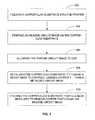
- FIG. 2is a flow chart showing one embodiment of steps of a method in accordance with the present invention.
- FIG. 3is a flow chart showing another embodiment of steps of a method in accordance with the present invention.
- FIG. 4is a block diagram of one embodiment of a printer in accordance with the present invention.
- the present inventionprovides a method and printer for inexpensively producing printed circuit boards by printing an inverse circuit image directly on a copper-clad substrate, metalizing the exposed, uninked copper surface and etching away copper that forms the inverse circuit image.
- the use of expensive photo-sensitive copperis not required, saving in the expense of materials needed to produce the circuit board.
- the copper-clad substrateshould be thoroughly cleaned before printing onto it.
- Chemical etchant solutionsmay include cupric chloride, ferric chloride, sodium peroxydisulfate, ammonium persulfate, ammoniacal cupric chloride, hydrochloric acid and nitric acid.
- all stripping solutionsare operative in the practice of this invention so long as they do not cause excessive attack of the tinned or metalized copper layer of the substrate.
- the etchantmay be sprayed onto the surface.
- etchingmay be accomplished at temperatures of 110 degrees Fahrenheit for a period of time determined by trial and error to be suitable for the particular implementation.
- typically useful etchants and process conditionssee U.S. Pat. No. 5,509,557, which is incorporated herein by reference in its entirety.
- the printer 100 , 400is arranged to accommodate a flat input of at least one substrate suitable for fabrication of a printed circuit board. That is, as shown in FIG. 1 and FIG. 4, paper may be fed into the printer 100 , 400 and exit the opposite side 408 . In addition, a copper-clad substrate 106 , 406 may be fed through the printer and exit the opposite side 408 .
- the width of the flat-input feed tray 102 , 402 for the substratemay be adjusted, for example, in the fashion that printers use to accommodate odd width paper inputs such as envelopes and postcards.
- the flat input feed tray 102 , 402may have a pressure feed that is adjustable (not shown) so that various thicknesses of substrates may be accommodated.
- the flat-input feed tray 102 , 402may simply be adjustable to various fixed settings that accommodate a plurality of desired substrate thicknesses. Since various types of pressure feeds and fixed setting feeds are known in the art, such arrangements will not be further described here.
- the copper-clad substrateis cleaned prior to printing the inverse circuit image thereon to facilitate better adhesion of the printer ink to the copper surface. Any selected suitable ink may be utilized. For example, India ink may be used to print the inverse circuit image. Cleaning may be accomplished by immersing the copper-clad substrate briefly in a suitable chemical bath, polishing, or the like.
- he printer 100 , 400may be coupled to a computing device (not shown) or may include a control panel for printing control.
- FIG. 2shows one embodiment of steps for an inexpensive method for producing a printed circuit board using a printer configured to print at least directly on a copper-clad substrate in accordance with the present invention.
- the stepsinclude feeding 202 a copper-clad substrate into the printer and then printing 204 an inverse circuit image on the copper-clad substrate.
- the inverse circuit imageis allowed 206 to dry.
- the copper-clad substratemay be immersed 208 in a tinning solution to adhere a resist mask to exposed, uninked copper so that a tinned circuit image is formed.
- the copper-clad substrateis then etched to remove the copper that forms the inverse circuit image.
- the printermay utilize water-insoluble ink.
- the input path for the printermay be adjustable to include at least two settings: a first setting to feed paper through a printing process and a second setting to accommodate a copper-clad substrate having a predetermined size.
- the width of the copper-clad substratemay be accommodated by utilizing moveable sides for the input tray as is known in the art for, for example, feeding envelopes or postcards into a printer.
- the setting for the input path for the printer to accommodate the copper-clad substratemay be further adjustable to accommodate a plurality of thicknesses of copper-clad substrates. Any suitable printer ink, such as for example, India ink, may be utilized.
- FIG. 3is a flow chart showing steps of another inexpensive method for producing a printed circuit board using a printer configured to facilitate printing at least directly on a copper-clad substrate in accordance with the present invention.
- the stepsinclude feeding 302 a copper-clad substrate into the printer, printing 304 an inverse circuit image on the copper-clad substrate, allowing 306 the inverse circuit image to dry, metalizing 308 the copper-clad substrate to adhere a resist mask to exposed, uninked copper to form a metalized circuit image, and etching 310 the copper-clad substrate that has been metalized to remove the copper that forms the inverse circuit image.
- water-insoluble inkmay be utilized.
- the input path for the printermay be adjustable to include at least a first setting to feed paper through a printing process and a second setting to accommodate a copper-clad substrate having a predetermined size.
- the settings for the input path for the printermay further include settings to accommodate a plurality of sizes of copper-clad substrates.
- copper-clad substrates of various widths and thicknessesmay be used.
- a library of inverse circuit imagesis stored on a computing device and is used to direct the printing process.
- Metalizing the copper-clad substrate to adhere a resist mask to exposed, uninked coppergenerally includes coating the exposed, uninked copper with another suitable metal such as manganese, chromium, aluminum, iron, cobalt, nickel, tin, zinc, cadmium, palladium, or lead. Also, alloys of the recited metals may be used. The metalization process may be accomplished by a number of methods, as is known in the art. For example, metalization may be accomplished by soldering, electro-plating or electroless plating.
- FIG. 4is a block diagram of a printer 400 configured to print at least directly on a copper-clad substrate to facilitate inexpensively producing a printed circuit board.
- the printerincludes an adjustable flat-input feed tray 402 for feeding at least a copper-clad substrate 406 into the printer and a printing mechanism 404 , proximate to the adjustable feeding mechanism 402 , arranged to provide for printing an inverse circuit image on the copper-clad substrate 406 wherein, after the image is printed, the inverse circuit image is allowed to dry, the copper-clad substrate 406 is immersed in a tinning solution to adhere a resist mask to exposed, uninked copper to form a tinned circuit image, and the copper-clad substrate 406 is etched to remove the copper that forms the inverse circuit image.
- the copper-clad substrate 406may be metalized to adhere a resist mask to exposed, uninked copper to form a metalized circuit image, and the copper-clad substrate that has been metalized is etched to remove copper that forms the inverse circuit image.
- water-insoluble inkmay be used.
- the adjustable feeding flat-input feed tray 402typically includes at least two settings: a first setting to feed paper through a printing process and a second setting to accommodate a copper-clad substrate having a predetermined size.
- an ink source for the printermay be removable, so that, where desired, different inks may be used to print on paper or copper-clad substrates.
- the input settingsmay include a plurality of fixed settings, or alternatively, may utilize a pressure-controlled input arranged to accommodate a plurality of sizes of copper-clad substrates.
- the usermay utilized any desired suitable ink, such as, for example, India ink.
- the printed inverse circuit diagramexposes the uninked copper, which may be metalized to adhere a resist mask using at least one of: manganese, chromium, aluminum, iron, cobalt, nickel, tin, zinc, cadmium, palladium and lead or an alloy thereof. Metalization may be accomplished via soldering, electro-plating, electroless plating or any other suitable technique.
Landscapes
- Engineering & Computer Science (AREA)
- Manufacturing & Machinery (AREA)
- Microelectronics & Electronic Packaging (AREA)
- Metallurgy (AREA)
- Manufacturing Of Printed Circuit Boards (AREA)
Abstract
Description
The present invention relates to printer capabilities, and more particularly to printers capable of “printing” etch resist directly to a metal to facilitate fabrication of printed circuit boards.
There are a number of methods for creating a printed circuit. In early fabrications of semiconductors, a photographic process was used to create a fine pattern of an integrated circuit, wherein each layer of the chip was defined by a specific mask. Typically, there could be 16-24 mask layers for each integrated circuit. Masks were typically stored in a chip design database. In one embodiment, each mask was made by placing a film of chromium in a pattern on a pure quartz glass plate. The finished plates were manufactured by very sophisticated pattern generating equipment. Patterns were formed by using a laser or electron-beam driven devices to remove chromium from the chromium-plated quartz so that only the desired pattern of chromium was left behind. This method was expensive.
In another type of fabrication, a photoresist has been used. A substrate is coated with copper, then coated with a layer of photoresist. A photoresist is a light-sensitive material that, on exposure to ultraviolet light, undergoes a chemical reaction much like the action of light on photographic film. When the photoresist is developed, a negative image of the mask is created. A chemical etchant may be applied to etch away the material that is not protected by the photoresist. Two types of photoresists may be used. If the photoresist hardens on exposure to light, when the excess resist is removed, a negative copy of the mask, commonly called a negative photoresist, is left behind.
Alternatively, a positive photoresist may be designed to degrade upon exposure to light. When developed, the photoresist is deposited in the areas where the light did not expose the resist, providing a positive copy of the mask. A liquid developer may be used to form a relief image, and a chemical etchant may be used to remove unwanted copper. The copper protected by the photoresist mask forms the desired circuit pattern. The photoresist is then peeled off, exposing the desired circuit pattern of copper.
Traditionally, in a small business environment, a library of masks is stored in memory of a computer, and a laser printer using toner may be used to print a mask of a desired circuit on a transparency. Generally, a substrate is coated with photo-sensitive copper. Alternatively, boards that have been coated with photo-sensitive copper may also be available from the marketplace. The transparency is placed over the photo-sensitive copper, and the inverse image of the circuit is burned into the resist for a time that typically has been determined by running a series of time-exposure tests on a sample of the photo-sensitive copper. The photo-sensitive copper that has the desired circuit burned into it is developed and etched. The etchant dissolves the unprotected copper off the board, leaving the desired circuit. This process is time-consuming, difficult, and costly. However, this method also has problems associated with it. The photo-resist typically has a limited shelf-life, and the necessary exposure time may vary depending on conditions. The process requires a dark room, two chemical baths, and expensive photo-sensitive copper.
Thus, there is a need for a less expensive, less complex process for preparing a printed circuit board.
The present invention provides a printer and an inexpensive method for producing a printed circuit board using a printer configured to facilitate printing at least directly on a copper-clad substrate. The method includes the steps of feeding a copper-clad substrate into the printer, printing an inverse circuit image on the copper-clad substrate, allowing the inverse circuit image to dry, metalizing the copper-clad substrate to adhere a resist mask to exposed, uninked copper to form a metalized circuit image, and etching the copper-clad substrate that has been metalized to remove copper that forms the inverse circuit image.
FIG. 1 is one embodiment of a representation of a printer that is configured to print flat input substrates in accordance with the present invention.
FIG. 2 is a flow chart showing one embodiment of steps of a method in accordance with the present invention.
FIG. 3 is a flow chart showing another embodiment of steps of a method in accordance with the present invention.
FIG. 4 is a block diagram of one embodiment of a printer in accordance with the present invention.
The present invention provides a method and printer for inexpensively producing printed circuit boards by printing an inverse circuit image directly on a copper-clad substrate, metalizing the exposed, uninked copper surface and etching away copper that forms the inverse circuit image. In the present invention, the use of expensive photo-sensitive copper is not required, saving in the expense of materials needed to produce the circuit board. For optimal results, the copper-clad substrate should be thoroughly cleaned before printing onto it.
Chemical etchant solutions may include cupric chloride, ferric chloride, sodium peroxydisulfate, ammonium persulfate, ammoniacal cupric chloride, hydrochloric acid and nitric acid. In general, all stripping solutions are operative in the practice of this invention so long as they do not cause excessive attack of the tinned or metalized copper layer of the substrate. For example, the etchant may be sprayed onto the surface. Where desired, etching may be accomplished at temperatures of 110 degrees Fahrenheit for a period of time determined by trial and error to be suitable for the particular implementation. For a discussion of typically useful etchants and process conditions, see U.S. Pat. No. 5,509,557, which is incorporated herein by reference in its entirety.
Theprinter printer opposite side 408. In addition, a copper-clad substrate opposite side 408. The width of the flat-input feed tray 102,402 for the substrate may be adjusted, for example, in the fashion that printers use to accommodate odd width paper inputs such as envelopes and postcards. The flatinput feed tray 102,402 may have a pressure feed that is adjustable (not shown) so that various thicknesses of substrates may be accommodated. Alternatively, the flat-input feed tray 102,402 may simply be adjustable to various fixed settings that accommodate a plurality of desired substrate thicknesses. Since various types of pressure feeds and fixed setting feeds are known in the art, such arrangements will not be further described here. Generally, the copper-clad substrate is cleaned prior to printing the inverse circuit image thereon to facilitate better adhesion of the printer ink to the copper surface. Any selected suitable ink may be utilized. For example, India ink may be used to print the inverse circuit image. Cleaning may be accomplished by immersing the copper-clad substrate briefly in a suitable chemical bath, polishing, or the like. As is known in the art, he printer100,400 may be coupled to a computing device (not shown) or may include a control panel for printing control.
FIG. 2 shows one embodiment of steps for an inexpensive method for producing a printed circuit board using a printer configured to print at least directly on a copper-clad substrate in accordance with the present invention. The steps include feeding202 a copper-clad substrate into the printer and then printing204 an inverse circuit image on the copper-clad substrate. The inverse circuit image is allowed206 to dry. Then, the copper-clad substrate may be immersed208 in a tinning solution to adhere a resist mask to exposed, uninked copper so that a tinned circuit image is formed. The copper-clad substrate is then etched to remove the copper that forms the inverse circuit image. Where desired, the printer may utilize water-insoluble ink.
Where desired, the input path for the printer may be adjustable to include at least two settings: a first setting to feed paper through a printing process and a second setting to accommodate a copper-clad substrate having a predetermined size. The width of the copper-clad substrate may be accommodated by utilizing moveable sides for the input tray as is known in the art for, for example, feeding envelopes or postcards into a printer. In addition, the setting for the input path for the printer to accommodate the copper-clad substrate may be further adjustable to accommodate a plurality of thicknesses of copper-clad substrates. Any suitable printer ink, such as for example, India ink, may be utilized.
FIG. 3 is a flow chart showing steps of another inexpensive method for producing a printed circuit board using a printer configured to facilitate printing at least directly on a copper-clad substrate in accordance with the present invention. The steps include feeding302 a copper-clad substrate into the printer, printing304 an inverse circuit image on the copper-clad substrate, allowing306 the inverse circuit image to dry, metalizing308 the copper-clad substrate to adhere a resist mask to exposed, uninked copper to form a metalized circuit image, andetching 310 the copper-clad substrate that has been metalized to remove the copper that forms the inverse circuit image. In a preferred embodiment, water-insoluble ink may be utilized. The input path for the printer may be adjustable to include at least a first setting to feed paper through a printing process and a second setting to accommodate a copper-clad substrate having a predetermined size. The settings for the input path for the printer may further include settings to accommodate a plurality of sizes of copper-clad substrates. Thus, as described above, copper-clad substrates of various widths and thicknesses may be used. Typically, a library of inverse circuit images is stored on a computing device and is used to direct the printing process.
Metalizing the copper-clad substrate to adhere a resist mask to exposed, uninked copper generally includes coating the exposed, uninked copper with another suitable metal such as manganese, chromium, aluminum, iron, cobalt, nickel, tin, zinc, cadmium, palladium, or lead. Also, alloys of the recited metals may be used. The metalization process may be accomplished by a number of methods, as is known in the art. For example, metalization may be accomplished by soldering, electro-plating or electroless plating.
FIG. 4 is a block diagram of aprinter 400 configured to print at least directly on a copper-clad substrate to facilitate inexpensively producing a printed circuit board. The printer includes an adjustable flat-input feed tray 402 for feeding at least a copper-cladsubstrate 406 into the printer and aprinting mechanism 404, proximate to theadjustable feeding mechanism 402, arranged to provide for printing an inverse circuit image on the copper-cladsubstrate 406 wherein, after the image is printed, the inverse circuit image is allowed to dry, the copper-cladsubstrate 406 is immersed in a tinning solution to adhere a resist mask to exposed, uninked copper to form a tinned circuit image, and the copper-cladsubstrate 406 is etched to remove the copper that forms the inverse circuit image. Thus, a tinned copper circuit image remains, providing a facilitated electrical connection. Alternatively, after the inverse circuit image is allowed to dry, the copper-cladsubstrate 406 may be metalized to adhere a resist mask to exposed, uninked copper to form a metalized circuit image, and the copper-clad substrate that has been metalized is etched to remove copper that forms the inverse circuit image. Typically, water-insoluble ink may be used. The adjustable feeding flat-input feed tray 402 typically includes at least two settings: a first setting to feed paper through a printing process and a second setting to accommodate a copper-clad substrate having a predetermined size. Also, an ink source for the printer may be removable, so that, where desired, different inks may be used to print on paper or copper-clad substrates. Where desired, where a plurality of input sizes are desired, the input settings may include a plurality of fixed settings, or alternatively, may utilize a pressure-controlled input arranged to accommodate a plurality of sizes of copper-clad substrates. Again, the user may utilized any desired suitable ink, such as, for example, India ink. After drying, the printed inverse circuit diagram exposes the uninked copper, which may be metalized to adhere a resist mask using at least one of: manganese, chromium, aluminum, iron, cobalt, nickel, tin, zinc, cadmium, palladium and lead or an alloy thereof. Metalization may be accomplished via soldering, electro-plating, electroless plating or any other suitable technique.
Thus, methods and printers have been described according to the present invention. Many modifications and variations may be made to the techniques and structures described and illustrated herein without departing from the spirit and scope of the invention. Accordingly, it should be understood that the methods and printers described herein are illustrative only and are not limiting upon the scope of the invention.
Claims (13)
1. An inexpensive method for producing a printed circuit board using a printer configured to facilitate printing at least directly on a copper-clad substrate, comprising the steps of:
feeding a copper-clad substrate into the printer;
printing an inverse circuit image on the copper-clad substrate;
allowing the inverse circuit image to dry;
immersing the copper-clad substrate in a tinning solution to adhere a resist mask to exposed, uninked copper to form a tinned circuit image; and
etching the copper-clad substrate to remove copper forming the inverse circuit image.
2. The method ofclaim 1 wherein the printer utilizes water-insoluble ink.
3. The method ofclaim 1 wherein the printer utilizes India ink.
4. The method ofclaim 1 wherein an input path for the printer is adjustable to include at least two settings: a first setting to feed paper through a printing process and a second setting to accommodate a copper-clad substrate having a predetermined size.
5. The method ofclaim 4 wherein the second setting for the input path for the printer to accommodate a copper-clad substrate is further adjustable to accommodate a plurality of sizes of copper-clad substrates.
6. An inexpensive method for producing a printed circuit board using a printer configured to facilitate printing at least directly on a copper-clad substrate, comprising the steps of:
feeding a copper-clad substrate into the printer;
printing an inverse circuit image on the copper-clad substrate;
allowing the inverse circuit image to dry;
metalizing the copper-clad substrate to adhere a resist mask to exposed, uninked copper to form a metalized circuit image; and
etching the copper-clad substrate that has been metalized to remove copper that forms the inverse circuit image.
7. The method ofclaim 6 wherein the printer utilizes water-insoluble ink.
8. The method ofclaim 6 wherein the printer utilizes India ink.
9. The method ofclaim 6 wherein an input path for the printer is adjustable to include at least two settings: a first setting to feed paper through a printing process and a second setting to accommodate a copper-clad substrate having a predetermined size.
10. The method ofclaim 9 wherein the at least two settings for the input path for the printer include settings to accommodate a plurality of sizes of copper-clad substrates.
11. The method ofclaim 6 wherein the step of metalizing the copper-clad substrate to adhere a resist mask to exposed, uninked copper includes coating the exposed, uninked copper with at least one of: manganese, chromium, aluminum, iron, cobalt, nickel, tin, zinc, cadmium, palladium, and lead.
12. The method ofclaim 6 wherein the step of metalizing the copper-clad substrate to adhere a resist mask to exposed, uninked copper includes coating the exposed, uninked copper with an alloy of at least one of: manganese, chromium, aluminum, iron, cobalt, tin, zinc, nickel, cadmium, palladium, and lead.
13. The method ofclaim 6 wherein the step of metalizing the copper-clad substrate to adhere a resist mask to exposed, uninked copper includes coating the exposed, uninked copper by one of: soldering, electro-plating and electroless plating.
Priority Applications (2)
| Application Number | Priority Date | Filing Date | Title |
|---|---|---|---|
| US10/040,086US6676991B2 (en) | 2001-10-29 | 2001-10-29 | Etch resist using printer technology |
| US10/716,274US6921550B2 (en) | 2001-10-29 | 2003-11-18 | Etch resist using printer technology |
Applications Claiming Priority (1)
| Application Number | Priority Date | Filing Date | Title |
|---|---|---|---|
| US10/040,086US6676991B2 (en) | 2001-10-29 | 2001-10-29 | Etch resist using printer technology |
Related Child Applications (1)
| Application Number | Title | Priority Date | Filing Date |
|---|---|---|---|
| US10/716,274DivisionUS6921550B2 (en) | 2001-10-29 | 2003-11-18 | Etch resist using printer technology |
Publications (2)
| Publication Number | Publication Date |
|---|---|
| US20030079624A1 US20030079624A1 (en) | 2003-05-01 |
| US6676991B2true US6676991B2 (en) | 2004-01-13 |
Family
ID=21909009
Family Applications (2)
| Application Number | Title | Priority Date | Filing Date |
|---|---|---|---|
| US10/040,086Expired - Fee RelatedUS6676991B2 (en) | 2001-10-29 | 2001-10-29 | Etch resist using printer technology |
| US10/716,274Expired - Fee RelatedUS6921550B2 (en) | 2001-10-29 | 2003-11-18 | Etch resist using printer technology |
Family Applications After (1)
| Application Number | Title | Priority Date | Filing Date |
|---|---|---|---|
| US10/716,274Expired - Fee RelatedUS6921550B2 (en) | 2001-10-29 | 2003-11-18 | Etch resist using printer technology |
Country Status (1)
| Country | Link |
|---|---|
| US (2) | US6676991B2 (en) |
Citations (11)
| Publication number | Priority date | Publication date | Assignee | Title |
|---|---|---|---|---|
| US3668003A (en)* | 1969-11-26 | 1972-06-06 | Cirkitrite Ltd | Printed circuits |
| US4049844A (en)* | 1974-09-27 | 1977-09-20 | General Electric Company | Method for making a circuit board and article made thereby |
| US4368281A (en)* | 1980-09-15 | 1983-01-11 | Amp Incorporated | Printed circuits |
| US4991287A (en)* | 1989-12-26 | 1991-02-12 | Eastman Kodak Company | Method for fabricating printed circuit boards |
| US5061551A (en)* | 1987-02-06 | 1991-10-29 | Key-Tech, Inc. | Printed circuit board |
| US5148355A (en)* | 1988-12-24 | 1992-09-15 | Technology Applications Company Limited | Method for making printed circuits |
| US5450286A (en)* | 1992-12-04 | 1995-09-12 | Parlex Corporation | Printed circuit having a dielectric covercoat |
| US5759269A (en)* | 1993-06-03 | 1998-06-02 | International Business Machines Corporation | Manufacturing flexible circuit board assemblies and printer for screening solder paste in such manufacture |
| US5826329A (en)* | 1995-12-19 | 1998-10-27 | Ncr Corporation | Method of making printed circuit board using thermal transfer techniques |
| US6109175A (en)* | 1997-02-21 | 2000-08-29 | Ricoh Microelectronics Co., Ltd. | Intaglio printing method, intaglio printer, method of formation of bumps or wiring pattern, apparatus therefor, bump electrode and printed circuit board |
| US6405647B2 (en)* | 1997-02-21 | 2002-06-18 | Ricoh Microelectronics Co., Ltd. | Intaglio printing method, intaglio printer and touch panel |
Family Cites Families (3)
| Publication number | Priority date | Publication date | Assignee | Title |
|---|---|---|---|---|
| US5151595A (en)* | 1990-10-16 | 1992-09-29 | Simon Marketing, Inc. | Imaging device and method for developing, duplicating and printing graphic media |
| US5774141A (en)* | 1995-10-26 | 1998-06-30 | Hewlett-Packard Company | Carriage-mounted inkjet aerosol reduction system |
| FR2775280B1 (en)* | 1998-02-23 | 2000-04-14 | Saint Gobain Vitrage | METHOD OF ETCHING A CONDUCTIVE LAYER |
- 2001
- 2001-10-29USUS10/040,086patent/US6676991B2/ennot_activeExpired - Fee Related
- 2003
- 2003-11-18USUS10/716,274patent/US6921550B2/ennot_activeExpired - Fee Related
Patent Citations (11)
| Publication number | Priority date | Publication date | Assignee | Title |
|---|---|---|---|---|
| US3668003A (en)* | 1969-11-26 | 1972-06-06 | Cirkitrite Ltd | Printed circuits |
| US4049844A (en)* | 1974-09-27 | 1977-09-20 | General Electric Company | Method for making a circuit board and article made thereby |
| US4368281A (en)* | 1980-09-15 | 1983-01-11 | Amp Incorporated | Printed circuits |
| US5061551A (en)* | 1987-02-06 | 1991-10-29 | Key-Tech, Inc. | Printed circuit board |
| US5148355A (en)* | 1988-12-24 | 1992-09-15 | Technology Applications Company Limited | Method for making printed circuits |
| US4991287A (en)* | 1989-12-26 | 1991-02-12 | Eastman Kodak Company | Method for fabricating printed circuit boards |
| US5450286A (en)* | 1992-12-04 | 1995-09-12 | Parlex Corporation | Printed circuit having a dielectric covercoat |
| US5759269A (en)* | 1993-06-03 | 1998-06-02 | International Business Machines Corporation | Manufacturing flexible circuit board assemblies and printer for screening solder paste in such manufacture |
| US5826329A (en)* | 1995-12-19 | 1998-10-27 | Ncr Corporation | Method of making printed circuit board using thermal transfer techniques |
| US6109175A (en)* | 1997-02-21 | 2000-08-29 | Ricoh Microelectronics Co., Ltd. | Intaglio printing method, intaglio printer, method of formation of bumps or wiring pattern, apparatus therefor, bump electrode and printed circuit board |
| US6405647B2 (en)* | 1997-02-21 | 2002-06-18 | Ricoh Microelectronics Co., Ltd. | Intaglio printing method, intaglio printer and touch panel |
Also Published As
| Publication number | Publication date |
|---|---|
| US20030079624A1 (en) | 2003-05-01 |
| US6921550B2 (en) | 2005-07-26 |
| US20040099167A1 (en) | 2004-05-27 |
Similar Documents
| Publication | Publication Date | Title |
|---|---|---|
| US5359928A (en) | Method for preparing and using a screen printing stencil having raised edges | |
| US4751172A (en) | Process for forming metal images | |
| CN100525582C (en) | Method of forming circuit pattern on printed circuit board | |
| US8293461B2 (en) | Direct emulsion process for making printed circuits | |
| US20070072129A1 (en) | Method for forming flexible printed circuit boards | |
| US6676991B2 (en) | Etch resist using printer technology | |
| US7754417B2 (en) | Printed circuits and method for making same | |
| US8313891B2 (en) | Printed circuits and method for making same | |
| JPH0537140A (en) | Method for manufacturing printed wiring board | |
| US5322763A (en) | Process for making metal ledge on stencil screen | |
| JP3017752B2 (en) | Printing metal mask and manufacturing method thereof | |
| JPS61144396A (en) | Screen plate-making | |
| JP2001326448A (en) | Method and device for forming etching resist pattern when circuit pattern is formed on printed board | |
| US5573815A (en) | Process for making improved metal stencil screens for screen printing | |
| JP2001332840A (en) | Manufacturing method of printed-wiring board | |
| JP3186256B2 (en) | Method for manufacturing flexible circuit board for TAB | |
| JPH0353587A (en) | Formation of resist pattern | |
| JPS58128788A (en) | Printed circuit board manufacturing method | |
| US5578186A (en) | Method for forming an acrylic resist on a substrate and a fabrication process of an electronic apparatus | |
| JPH04334084A (en) | Manufacture of wiring board | |
| JP2002223059A (en) | Fine pattern forming method | |
| JP4421706B2 (en) | Method for manufacturing metal part having plating pattern on surface | |
| JPS59231887A (en) | Method for etching picture line on irregular surface or flatsurface of printed board or the like using uv ink | |
| Ruckert | New Light‐Sensitive Positive‐Working Thick Resist Materials for Various Electronic Applications | |
| Uematsu | High sensitivity dry film photoresist for laser direct imaging system |
Legal Events
| Date | Code | Title | Description |
|---|---|---|---|
| AS | Assignment | Owner name:HEWLETT-PACKARD COMPANY, COLORADO Free format text:ASSIGNMENT OF ASSIGNORS INTEREST;ASSIGNOR:DEHAVEN, MAXWELL S.;REEL/FRAME:012460/0283 Effective date:20011024 | |
| AS | Assignment | Owner name:HEWLETT-PACKARD DEVELOPMENT COMPANY L.P., TEXAS Free format text:ASSIGNMENT OF ASSIGNORS INTEREST;ASSIGNOR:HEWLETT-PACKARD COMPANY;REEL/FRAME:014061/0492 Effective date:20030926 Owner name:HEWLETT-PACKARD DEVELOPMENT COMPANY L.P.,TEXAS Free format text:ASSIGNMENT OF ASSIGNORS INTEREST;ASSIGNOR:HEWLETT-PACKARD COMPANY;REEL/FRAME:014061/0492 Effective date:20030926 | |
| FPAY | Fee payment | Year of fee payment:4 | |
| FPAY | Fee payment | Year of fee payment:8 | |
| REMI | Maintenance fee reminder mailed | ||
| LAPS | Lapse for failure to pay maintenance fees | ||
| STCH | Information on status: patent discontinuation | Free format text:PATENT EXPIRED DUE TO NONPAYMENT OF MAINTENANCE FEES UNDER 37 CFR 1.362 | |
| FP | Expired due to failure to pay maintenance fee | Effective date:20160113 |